Embed Size (px)
Citation preview
PARAMETRIC AVERAGE VALUE MODELING OF FLYBACK CONVER TERS IN
CCM AND DCM INCLUDING PARASITICS AND SNUBBERS
by
Mehmet Sucu
B.A.Sc., Marmara University, 2000 M.A.Sc., Marmara University, 2003
A THESIS SUBMITTED IN PARTIAL FULFILLMENT OF
THE REQUIREMENTS FOR THE DEGREE OF
MASTER OF APPLIED SCIENCE
in
THE FACULTY OF GRADUATE STUDIES
(ELECTRICAL AND COMPUTER ENGINEERING)
THE UNIVERSITY OF BRITISH COLUMBIA
(Vancouver)
October 2011
© Mehmet Sucu, 2011

ii
Abstract
Modeling of switched-mode DC-DC converters has been receiving significant interest due to
their widespread applications. Averaged modeling is the most common approach (and tool)
that has been used to analyze dynamic performance of converter circuits. Specifically, state-
space averaged models are widely used because of their simplicity and generality. However,
as has been shown in the literature, the challenges of directly applying this approach to
predict the discontinuous variables (states) and include the parasitics and losses have limited
application of this approach to a wider range of converter circuits. The recently introduced
parametric average value models (PAVM) has a potential to overcome this problem.
In this Thesis, first of all a second-order flyback converter has been investigated. An
analytical solution of state-apace averaging and small-signal analysis of the flyback converter
in continuous conduction mode (CCM) and discontinuous conduction mode (DCM) is given
without and with parasitics. The PAVM methodology has been applied to the second-order
model to overcome the problem of discontinuous state during the DCM.
The snubber circuits in flyback converter have also been investigated. Appearance of
snubbers in the model introduces a problem on the output voltage besides improving the
efficiency prediction. It is shown that with the snubbers the conventional state-space
averaging cannot predict the output voltage correctly in CCM and DCM. To solve this
problem the model is partitioned into two different sub-circuits: i) switching sub-circuit
circuit; and ii) non-switching sub-circuit. Thereafter it becomes possible apply the averaging
on the switching sub-circuit only.
Finally, a full-order flyback converter with two RC snubber circuits and all the basic
parasitics is considered. The PAVM methodology has been extended to this class of
switching converter for the first time. It is shown that including the snubbers and parasitics
significantly improves the model accuracy in terms of predicting converter efficiency, which
represents an appreciable improvement over all previously existing average models. The
proposed model has been verified with detailed simulations and hardware measurements.

iii
Table of Contents
Abstract .................................................................................................................................... ii
Table of Contents ................................................................................................................... iii
List of Tables ........................................................................................................................... v
List of Figures ......................................................................................................................... vi
List of Abbreviations ............................................................................................................. ix
Acknowledgements ................................................................................................................. x
Chapter 1 : Introduction ........................................................................................................ 1
1.1 PWM DC-DC Converters ..................................................................................................... 1
1.2 Flyback Converters ............................................................................................................... 1
1.3 Average Value Modeling ...................................................................................................... 2
1.4 Parametric Average-Value Modeling ................................................................................... 4
1.5 Motivations and Objectives .................................................................................................. 4
Chapter 2 : Second Order Flyback Converters ................................................................... 5
2.1 Small-Signal AC Model and State-Space Averaging without Parasitics in CCM ................ 5
2.2 State-Space Averaging in DCM without Parasitics ............................................................ 15
2.3 Small-Signal AC Model and State-Space Averaging with Basic Parasitics in CCM ......... 19
2.4 State-Space Averaging with Parasitics in DCM ................................................................. 32
2.5 Parametric Average Value Modeling in CCM and DCM ................................................... 36
2.5.1 Correction Term ............................................................................................................. 37
2.5.2 Model Implementation .................................................................................................... 38
2.5.3 Case Studies .................................................................................................................... 43
2.5.3.1 Time domain .......................................................................................................... 43
2.5.3.2 Frequency domain .................................................................................................. 45
Chapter 3 : Analysis of Flyback Converter with Snubber Circuits ................................. 47
3.1 Fifth –order Flyback Converter with Snubbers ................................................................... 47
3.2 State-Space Averaging Phenomena with the Snubbers ....................................................... 49
Chapter 4 : Full-order Flyback Converter ......................................................................... 56
4.1 State-Space Averaging in CCM .......................................................................................... 56
4.2 State-Space Averaging in DCM .......................................................................................... 59

iv
4.3 Parametric Average Value Modeling in CCM and DCM ................................................... 62
4.3.1 Model Implementation .................................................................................................... 62
4.4 Case Studies ........................................................................................................................ 67
4.4.1 Time Domain .................................................................................................................. 67
4.4.2 Frequency Domain.......................................................................................................... 69
4.4.3 Efficiency Results ........................................................................................................... 70
Chapter 5 : Conclusion ......................................................................................................... 72
5.1 Future Work ........................................................................................................................ 72
Bibliography .......................................................................................................................... 74
Appendices ............................................................................................................................. 78
Appendix A. The Converters Circuit Parameters .......................................................................... 78
A.1 Second-order Flyback Converter Parameters without Parasitics in CCM ...................... 78
A.2 Second-order Flyback Converter Parameters without Parasitics in DCM ...................... 78
A.3 Second-order Flyback Converter Parameters with Parasitics in CCM ........................... 78
A.4 Second-order Flyback Converter Parameters with Parasitics in DCM ........................... 79
A.5 Fifth-order Flyback Converter Parameters in CCM ....................................................... 79
A.6 Full-order Flyback Converter Parameters in CCM ......................................................... 79
A.7 Full-order Flyback Converter Parameters in DCM ........................................................ 80
Appendix B. Flyback Converter Circuit Diagram ......................................................................... 81

v
List of Tables
Table 4.1 Efficiency comparison of the average-value models .............................................. 71

vi
List of Figures
Figure 2.1 (a) Assumed circuit for the second order Flyback converter without
parasitics; (b) Circuit during subinterval 1; (c) Circuit during
subinterval 2. .......................................................................................................... 6
Figure 2.2 The inductor current ................................................................................................ 6
Figure 2.3 Inductor current and capacitor voltage of second order Flyback
converter without parasitics in CCM. .................................................................. 14
Figure 2.4 Capacitor voltage of second order Flyback converter without parasitics
in CCM. ................................................................................................................ 14
Figure 2.5 Second-order Flyback converter without parasitics during third
subinterval in DCM. ............................................................................................. 15
Figure 2.6 Magnetizing current in DCM for the load 2500R= Ω . ......................................... 16
Figure 2.7 Inductor current and capacitor voltage of second order Flyback
converter without parasitics in DCM. .................................................................. 18
Figure 2.8(a) Second-order Flyback converter with parasitics; (b) Circuit during
subinterval 1 (c) Circuit during subinterval 2. ..................................................... 19
Figure 2.9 Inductor current, capacitor voltage and output voltage of second order
Flyback converter with parasitics in CCM. ......................................................... 31
Figure 2.10 Output voltage of second order Flyback converter with parasitics in
CCM. .................................................................................................................... 31
Figure 2.11 Second-order Flyback converter with parasitics during third
subinterval in DCM. ............................................................................................. 32
Figure 2.12 Inductor current, capacitor voltage and output voltage of second
order Flyback converter with parasitics in DCM. ................................................ 35
Figure 2.13 Variable 3d as a function` of duty-cycle ( )1d and the load ( )R . ....................... 40
Figure 2.14 The correction term 1m as a function of duty-cycle ( )1d and the load
resistance ( )R . ..................................................................................................... 40
Figure 2.15 The correction term 2m as a function of duty-cycle ( )1d and the load
resistance ( )R . ..................................................................................................... 41

vii
Figure 2.16 Implementation of the parametric average-value model. .................................... 42
Figure 2.17 Simulated inductor current, capacitor voltage and output voltage of
the second order Flyback converter with parasitics in DCM. .............................. 44
Figure 2.18 Transients in inductor current, capacitor voltage and output voltage
of the second order Flyback converter due to the step change in load. ............... 45
Figure 2.19 Control-to-output transfer function of the second-order Flyback
converter evaluated at 717.05R= Ω and 1 0.381d = . ............................................. 46
Figure 3.1 Fifth-order Flyback converter circuit. ................................................................... 47
Figure 3.2 Measured transformer secondary voltage: (a) without the diode
snubber; and (b) with the diode snubber. ............................................................. 48
Figure 3.3 Simulated output filter capacitor voltage and the output voltage of the
fifth-order Flyback converter with snubbers in CCM. ......................................... 50
Figure 3.4 The predicted secondary current and the diode snubber capacitor
voltage of fifth-order Flyback converter in CCM. ............................................... 51
Figure 3.5 Forth-order Flyback converter without diode snubber. ......................................... 52
Figure 3.6 The simulated output filter capacitor and output voltage of the forth-
order Flyback converter without the diode snubber in CCM. .............................. 53
Figure 3.7 Modified fifth-order Flyback converter circuit. .................................................... 54
Figure 3.8 Proposed state-space averaged model of the fifth-order Flyback
converter using two sub-circuits and sub-models. ............................................... 54
Figure 4.1 Full-order Flyback converter circuit. ..................................................................... 56
Figure 4.2 Predicted state variables of full-order Flyback converter in CCM. ....................... 58
Figure 4.3 Simulated state variables of the full-order Flyback converter in DCM. ............... 60
Figure 4.4 Simulated transformer secondary current of the full-order Flyback
converter in DCM. ............................................................................................... 61
Figure 4.5 The diode current waveform. ................................................................................ 63

viii
Figure 4.6 Variable 3d as a function of the duty-cycle ( )1d and the load
resistance ( )R . ..................................................................................................... 64
Figure 4.7 The correction term 2m as a function of duty-cycle ( )1d and the load
resistance ( )R . ..................................................................................................... 65
Figure 4.8 The correction term 3m as a function of the duty-cycle ( )1d and the
load resistance ( )R . ............................................................................................. 65
Figure 4.9 The correction term 4m as a function of duty-cycle ( )1d and the load
resistance ( )R . ..................................................................................................... 66
Figure 4.10 The correction term 5m as a function of duty-cycle ( )1d and the load
resistance ( )R . ..................................................................................................... 67
Figure 4.11 Measured and simulated output voltage, primary and secondary
current in CCM at constant duty-cycle. ............................................................... 68
Figure 4.12 Simulated output voltage, primary and secondary current during the
transient from DCM to CCM due to the step change in load. ............................. 69
Figure 4.13 Control-to-output transfer function of the full-order Flyback
converter evaluated at 717.05R= Ω and 1 0.381d = ............................................... 70

ix
List of Abbreviations
CCM Continuous Conduction Mode
DCM Discontinuous Conduction Mode
PAVM Parametric Average Value Modeling
PWM Pulse Width Modulation

x
Acknowledgements
I would like to express my appreciation to my supervisor, Dr. Juri Jatskevich, whose strong
academic support have been the most precious assets to my studies and research. I am also
very grateful for the partial financial support that has been made available to me through the
NSERC under the Discovery Grant.
I also like to thank Dr. William Dunford and Dr. Shahriar Mirabbasi who have accepted to be
the committee members and dedicated their time and effort for reading this thesis and
providing their constructive and valuable comments.
My special thanks go to previous and current members of the Power and Energy Systems
Group at UBC who have always supported me and gave their valuable insights into my
research.

1
Chapter 1 : Introduction
1.1 PWM DC-DC Converters
Switch mode dc-dc converters have become an essential element of many commercial and
military applications. Due to their high efficiency, light weight and relatively low cost, the
switching dc-dc converters have generated a significant research interest in the area of their
modeling, analysis, and control. Among various types of dc-dc converters, the Pulse-Width
Modulated (PWM) converters constitute by far the largest group. They have displaced
conventional linear power supplies even at low power levels. Switch-mode dc-dc converters
can be categorized as non-linear periodic time-variant systems due to their inherent switching
operation. The topology depends on instantaneous states of the power switches. This is what
makes their modeling a complex task. Nevertheless, accurate analytical models of PWM dc-
dc converters are essential for the analysis and design in many applications e.g., automobiles,
aeronautics, aerospace, telecommunications, submarines, naval ships, mainframe computers
and medical equipments. Many efforts have been made in the past few decades to model dc-
dc converters and several new models have been proposed. These models are widely used to
study the static and dynamic characteristics of the converters as well as to design their
control systems to achieve specific regulation characteristics [1-8].
1.2 Flyback Converters
A flyback converter is a switching power supply topology widely used in low power
applications such as chargers and PC power supplies. It is basically an implementation of
buck-boost converter and has transformer isolation. The most important advantage is that it
becomes possible to have multiple outputs with a simple modification on the transformer
(adding another secondary winding) and adding few extra components (a diode and a filter
capacitor). Another important advantage is that it has natural isolation between input and
output, which is required by many standards for design of power supplies [9-13].
A detailed model of a flyback converter can be easily implemented using widely available
simulation packages (e.g. Matlab/Simulink, ASMG, PLECS, etc.) [14-16]. Detailed models
are often used during the design process as such models have all the required information to

2
calculate the exact switching transients and component stresses and characteristics. But the
large computation time required for such detailed switching models makes them less
applicable for system-level studies. Instead, the average-value modeling has been used very
effectively for the system-level analysis and studies, wherein the effects of fast switching are
neglected or averaged with respect to the switching interval. A classical state-space averaged
model of a flyback converter [10] considers only the switch losses without any snubber
circuits and has the simplest first-order transformer approximation. A simplified linear circuit
model for obtaining dc and small-signal circuit model is given in [17], which has the basic
parasitics but does not include any snubber circuits and transformer primary and secondary
copper losses. A dc and small-signal circuit model models for a flyback converter operating
in CCM can be found in [12], which has the basic parasitics but again does not include any
snubber circuits and has only a the simplest transformer model without the primary and
secondary losses.
1.3 Average Value Modeling
The averaged-value modeling, wherein the effects of fast switching are “averaged” over a
switching interval, is most frequently applied when investigating power-electronics-based
systems. Continuous large-signal models are typically non-linear and can be linearized
around a desired operating point. Averaged models of dc-dc converters offer several
advantages over the switching models. These advantages are: i) straightforward approach in
determining local transfer-functions; ii) faster simulation of large-signal system-level
transients; and iii) use of general-purpose simulators to linearize converters for designing the
feedback controllers.
A typical switched-inductor dc-dc converter can operate in two modes. One is the
Continuous Conduction Mode (CCM) in which inductor current never falls to zero, and the
second mode is Discontinuous Conduction Mode (DCM) allowing inductor current to
become zero for a portion of switching period. The DCM typically occurs at light loads and
differs from CCM since this mode results into three different switched networks over one
switching cycle (as opposed to two switched networks in the case of CCM operation).
Models for PWM converters operating in CCM based on well-known state-space averaging

3
technique were first introduced in 1970’s [18]. Since then, several circuit-oriented averaging
approaches have also been proposed [3, 19]. Numerous method have been developed for the
average value modeling of PWM dc-dc converters in DCM such as reduced-order state-space
averaging [20], reduced-order averaged-switch modeling [7], equivalent duty ratio models
[3], loss-free resistor model [10], full-order averaged-switch modeling [21], and full-order
state-space averaging [4].
Average value models may be categorized as resulting system of equations (reduced-order
vs. full order); or by derivation methodology (sampled data modeling, circuit averaging,
state-space averaging). The full-order as well as reduced-order models can be obtained by
averaging approaches including sampled data modeling, circuit averaging or state space
averaging. The conventional reduced order models treat the discontinuous variable as a
dependent variable and eliminate its dynamic from the state equations. The elimination of
fast/discontinuous variable is undesirable for application in which this variable is used for
control purposes, which limits the range of applications of such reduced-order models.
State-space averaging is based on the classical averaging theory and involves manipulation of
state-space equations of a converter system. First, a state-space representation of converter is
obtained for each topology and subinterval. Then, the obtained piece-wise linear equations
are weighted by the corresponding time subinterval length and added together. State-space
averaging has been demonstrated to be an effective method to analyze PWM converters.
Analytical averaging, however, is based on so-called small-ripple approximation. Most of the
previous works on averaging methods were derived for a specific ideal topology. In addition,
derivation of state-space average-value model, the equivalent series resistance (ESR) of
circuit components are often neglected and the state variables are considered as linear
segments. Such assumptions result in inaccuracy of the corresponding time constants as well
as the waveforms. If the losses due to the switch and/or active elements are taken into
account, whereby the linear shape of the current waveform would change into exponential
form, the analytically derived models would become significantly more complicated and
challenging. The analytical derivation also becomes more complicated when the number of
energy storage elements (inductors and capacitors) is high.

4
1.4 Parametric Average-Value Modeling
Parametric average-value modeling methodology has been set forth by the UBC researchers.
This methodology has been successfully demonstrated for synchronous machine-converter
systems in [22, 23]. The major point of this approach is to use the detailed simulation for
numerically calculating the key relationships needed for constructing the average-value
model of a certain well-defined form. In doing so, the effect of parasitics included in the
detailed model becomes automatically included in the numerically constructed parametric
functions, which are then used for the state-variable-based average-value models. This
approach also reduces the effort of the model developer and avoids many complicated
analytical derivations. This method has been extended to the PWM dc-dc converters in [24-
27] based on corrected full-order averaged models proposed for circuit averaging [28] and
state-space averaging [4] that very accurately capture the high-frequency dynamics of fast
state variables.
1.5 Motivations and Objectives
The detailed models of PWM dc-dc converters are widely used for design purposes but they
are not desirable for system level studies due to very high computational times, wherein it
has been always required to have more efficient average models. Although there are various
averaged models of the flyback PWM converter available, none of the previously established
models have full order and include all realistic parasitics. Most of the models use the simplest
transformer representation and none of them include the snubber circuits. At the same time,
the snubber circuits are very important components of the flyback PWM converters and have
significant effect on the converter dynamics and efficiency.
This Thesis makes an original contribution and extends the parametric average-value
modeling the flyback converters. The considered converter model includes all the basic
parasitics and high order transformer model with primary and secondary resistances and
leakage inductances. The propose model also includes two RC (resistance and capacitance)
snubber circuits to protect the switch and the diode during the on-off operation. To the best
of our knowledge, this has not been done in any published research on this subject.

5
Chapter 2 : Second Order Flyback Converters
In this Chapter, we consider and approximate (simplified) circuit of the flyback converter,
wherein only two energy storage elements are considered, hence second order converter.
Such approximate converter circuit has been used in the literature for carrying out basic
analysis and averaging methods. A number of modeling techniques have appeared in the
literature, including the current injected approach [19], circuit averaging [7, 21, 29], and
state-space averaging [18] method.
2.1 Small-Signal AC Model and State-Space Averaging without Parasitics in CCM
The state-space description of dynamical systems is a basis of modern control theory. The
state-space averaging method makes use of this description to derive the small-signal
averaged equations of the PWM switching converters. The state-space averaging method is
otherwise identical to the procedure of deriving the small-signal ac model. A benefit of the
state-space averaging procedure is its results: a small-signal averaged model that can always
be obtained, provided that the state equations of the original converter can be written.
Obtaining a small-signal ac model of a basic switched converter circuit, such as buck, boost
without parasitics, can be readily achieved using analytical derivations. But when the
converter circuit has parasitics, it becomes almost impossible and impractical to derive the
higher order state equations. In this case, the state-space equations can be obtained from the
detailed model by using commercially available simulation packages [16, 30], and then used
the state-space description (matrices) to establish the small-signal model [10] (see
Section7.3.2).
In this Section, a small-signal ac model will be derived for a second-order flyback converters
without parasitics. Based on that, the state-space equations will be derived.
A second order flyback converter without parasitics is shown in Figure 2.1(a). Here, n is the
turn ratio of the transformer( )1 2N N .

6
+
mL
n( )i t( )gi t( )ci t
( )v t( )Lv t
C R
D
Mosfet
+
mL
n( )i t( )gi t( )ci t
( )v t( )Lv t
C R
+
mL
n( )i t( )gi t( )ci t
( )v t( )Lv t
C R
( )a
( )b
( )c
( )gv t
( )gv t
( )gv t
Figure 2.1 (a) Assumed circuit for the second order Flyback converter without parasitics; (b) Circuit
during subinterval 1; (c) Circuit during subinterval 2.
The inductor current ( )i t in CCM is shown in Figure 2.2. During the first interval, Figure
2.1(b), the inductor stores some energy and transfers this energy to the secondary side during
the second interval, Figure 2.1(c).
0.4
0.6
0.8
1
1.2
1.4
1.6
I (A
mp.)
0.999991 0.999993 0.999995 0.999997
Time (s)
1 sd T2 sd T
sT
Figure 2.2 The inductor current

7
During the first subinterval, when the MOSFET conducts and the diode is off, the circuit
reduces to Figure 2.1(b). The inductor voltage ( )Lv t , capacitor current ( )ci t , and converter
input current ( )gi t can be expressed as follows:
( ) ( )L gv t v t= (2.1)
( ) ( )c
v ti t
R= − (2.2)
( ) ( )gi t i t= (2.3)
Applying the small ripple approximation [10] and replacing the voltages and currents with
their respective average values, we obtain
( ) ( )s
L g Tv t v t= (2.4)
( )( )
sT
c
v ti t
R= − (2.5)
( ) ( )s
g Ti t i t= (2.6)
During the second subinterval, MOSFET is off and the diode conducts, which results in
circuit of Figure 2.1(c). The inductor voltage ( )Lv t , capacitor current ( )ci t , and converter
input current ( )gi t are given by
( ) ( )Lv t v t n= (2.7)
( ) ( ) ( )c
v ti t i t n
R
= − +
(2.8)
( ) 0gi t = (2.9)
The small ripple approximation leads to
( ) ( )s
L Tv t v t n= (2.10)
( ) ( )( )
s
s
T
c T
v ti t i t n
R= − − (2.11)
( ) 0gi t = (2.12)
The average inductor voltage now can be found by averaging the subintervals over one
complete switching period. The result is
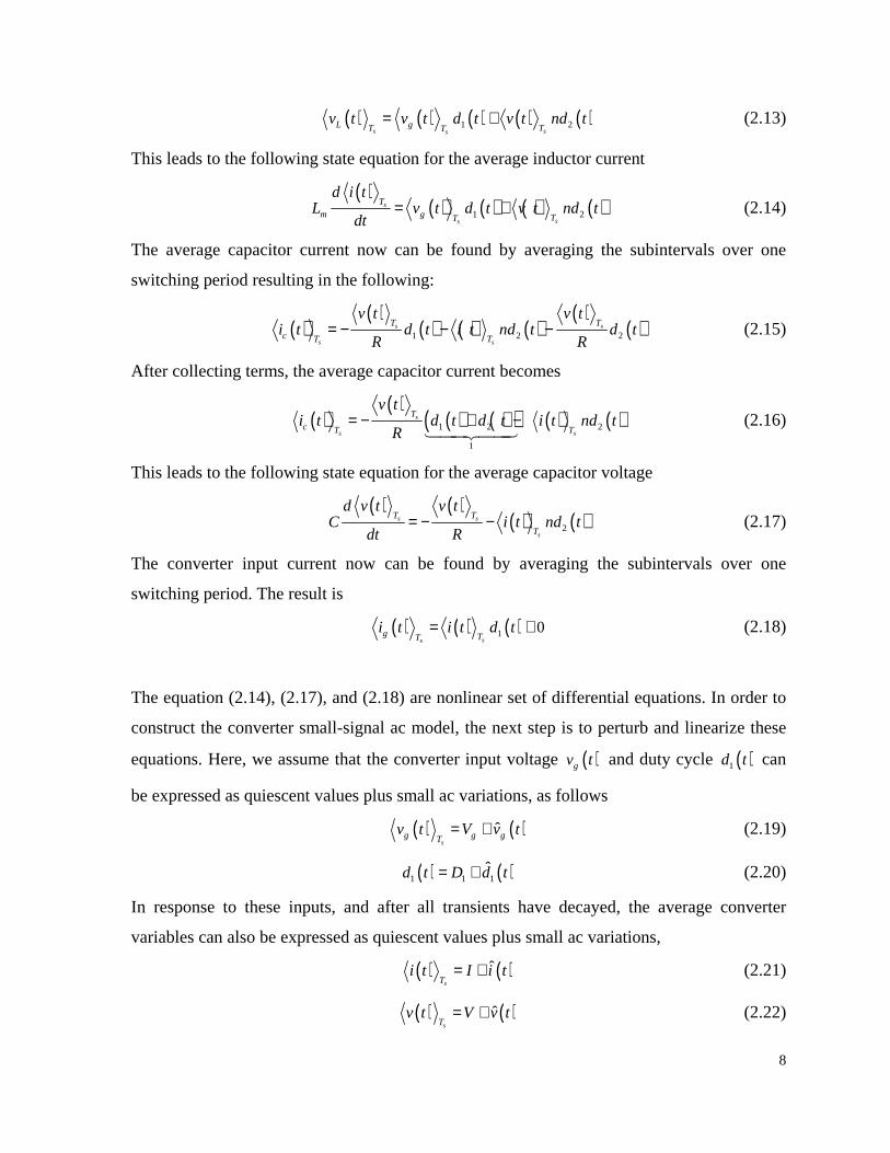
8
( ) ( ) ( ) ( ) ( )1 2s ss
L gT TTv t v t d t v t nd t= + (2.13)
This leads to the following state equation for the average inductor current
( )
( ) ( ) ( ) ( )1 2s
ss
T
m g TT
d i tL v t d t v t nd t
dt= + (2.14)
The average capacitor current now can be found by averaging the subintervals over one
switching period resulting in the following:
( )( )
( ) ( ) ( )( )
( )1 2 2s s
s s
T T
c T T
v t v ti t d t i t nd t d t
R R= − − − (2.15)
After collecting terms, the average capacitor current becomes
( )( )
( ) ( )( ) ( ) ( )1 2 2
1
s
s s
Tc T T
v ti t d t d t i t nd t
R= − + −
1442443 (2.16)
This leads to the following state equation for the average capacitor voltage
( ) ( )
( ) ( )2s s
s
T T
T
d v t v tC i t nd t
dt R= − − (2.17)
The converter input current now can be found by averaging the subintervals over one
switching period. The result is
( ) ( ) ( )1 0ss
g TTi t i t d t= + (2.18)
The equation (2.14), (2.17), and (2.18) are nonlinear set of differential equations. In order to
construct the converter small-signal ac model, the next step is to perturb and linearize these
equations. Here, we assume that the converter input voltage ( )gv t and duty cycle ( )1d t can
be expressed as quiescent values plus small ac variations, as follows
( ) ( )ˆs
g g gTv t V v t= + (2.19)
( ) ( )1 1 1ˆd t D d t= + (2.20)
In response to these inputs, and after all transients have decayed, the average converter
variables can also be expressed as quiescent values plus small ac variations,
( ) ( )ˆsT
i t I i t= + (2.21)
( ) ( )ˆsT
v t V v t= + (2.22)

9
( ) ( )ˆs
g g gTi t I i t= + (2.23)
With these substitutions, the large-signal averaged inductor equation (2.14) becomes
( )( ) ( )( ) ( )( ) ( )( ) ( )( )1 1 2 1
ˆˆ ˆˆ ˆm g g
d I i tL V v t D d t V v t n D d t
dt
+= + + + + − (2.24)
Upon multiplying this expression out and collecting terms, we obtain
( ) ( ) ( ) ( ) ( ) ( )( )
( ) ( ) ( ) ( )( )
1 2 1 1 1 2
1 ( )
1 1
2 ( )
ˆˆ ˆˆ ˆ
ˆ ˆˆ ˆ
m g g g
Dcterms st order acterms linear
g
nd order acterms nonlinear
di tdIL V D VnD V d t v t D Vnd t v t nD
dt dt
v t d t v t nd t
+ = + + + − +
+ −
1442443 14444444244444443
14444244443
(2.25)
As usual, this equation contains three types of terms. The dc term contain no time-varying
quantities. The first order ac terms are linear functions of the ac variations in the circuit,
while the second order ac terms are functions of the products of the ac variations. At this
point, we make an assumption that the ac variations are small in magnitude compared to the
dc quiescent values,
( )( )
( )( )( )
1 1
ˆ
ˆ
ˆ
ˆ
ˆ
g g
g g
v t V
d t D
i t I
v t V
i t I
<<<<<<
<<
<<
(2.26)
If the small signal assumptions (2.26) are satisfied, then the second-order terms are much
smaller in magnitude than the first-order terms and hence can be neglected. The dc terms
must satisfy
1 20 gV D VnD= + (2.27)
The first order ac terms must satisfy
( ) ( ) ( ) ( ) ( )1 1 1 2
ˆˆ ˆˆ ˆm g g
di tL V d t v t D Vnd t v t nD
dt= + − + (2.28)
This result is the linearized equation that describes ac variations in the inductor current.

10
Upon substation of (2.19), (2.20), (2.21), (2.22), and (2.23) into the averaged capacitor
voltage state equation (2.17), we obtain the following
( )( ) ( )( ) ( )( ) ( )( )2 1
ˆ ˆ ˆˆd V v t V v t
C I i t n D d tdt R
+ += − − + − (2.29)
Upon multiplying this expression out and collecting terms, we obtain
( ) ( ) ( ) ( )
( ) ( )( )
2 1 2
1 ( )
1
2 ( )
ˆ ˆ ˆ ˆ
ˆˆ
Dcterms st order acterms linear
nd order acterms nonlinear
dv t v tdV VC InD Ind t i t nD
dt dt R R
i t nd t
+ = − − + − + −
+
1442443 1444442444443
1442443
(2.30)
Here, we neglect the second-order terms. The dc terms of equation (2.30) must satisfy
20V
InDR
= − − (2.31)
The first-order ac terms of (2.30) lead to the small-signal ac state equation for capacitor
voltage
( ) ( ) ( ) ( )1 2
ˆ ˆ ˆ ˆdv t v tC Ind t i t nD
dt R= − + − (2.32)
Substation of (2.19), (2.20), (2.21), (2.22), and (2.23) into (2.18) results in the following:
( ) ( )( ) ( )( )1 1ˆˆ ˆ
g gI i t I i t D d t+ = + + (2.33)
Upon multiplying this expression out and collecting terms, we obtain
( ) ( )
( ) ( )( ) ( ) ( )( )1 1 1 1
1 ( ) 2 ( )
ˆ ˆˆ ˆ ˆg g
Dctermsst order acterms linear nd order acterms nonlinear
I i t ID Id t i t D i t d t+ = + + +1442443 14243
(2.34)
The dc term must satisfy
1gI ID= (2.35)
We neglect the second-order terms in (2.34), leaving the following linearized ac equation
( ) ( ) ( )1 1ˆˆ ˆ
gi t Id t i t D= + (2.36)
This result represents the low-frequency ac variations in the converter input current.
The equation of the quiescent values, (2.27), (2.31), and (2.35) are collected below,

11
1 2
2
1
0
0
g
g
V D VnD
VInD
RI ID
= + = − −
=
(2.37)
For given quiescent values of the input voltage gV , and duty cycle 1D , the system of
equations (2.37) can be evaluated to find the quiescent output voltage V , inductor current I ,
and input current dc component gI . The results are then inserted into the small-signal ac
model. The final small signal ac model is summarized below,
( ) ( ) ( ) ( ) ( )
( ) ( ) ( ) ( )
( ) ( ) ( )
1 1 1 2
1 2
1 1
ˆˆ ˆˆ ˆ
ˆ ˆ ˆ ˆ
ˆˆ ˆ
m g g
g
di tL V d t v t D Vnd t v t nD
dtdv t v t
C Ind t i t nDdt R
i t Id t i t D
= + − +
= − + − = +
(2.38)
The final step is to construct an equivalent circuit of (2.37) and (2.38) using commercially
available simulation tools.
Let us now apply the state-space averaging method to the second order flyback converter
circuit depicted in Figure 2.1(a). The independent state variables of the converter are the
inductor current ( )i t and the capacitor voltage ( )v t , which form the state vector
( ) ( )( )
i tx t
v t
=
(2.39)
The input voltage ( )gv t , is an independent source which should be placed in the input vector,
( ) ( )gu t v t = (2.40)
To model the converter as a system with input and output, we need to find the converter input
current ( )gi t . To calculate this dependent current, it should be included in the output vector
( )y t . Therefore,
( ) ( )gy t i t = (2.41)
Note that it’s not necessary to include the output voltage ( )v t in the output vector since the
voltage is already included in the state vector ( )x t .

12
Next, let us write the state equations for each subinterval. When the switch is on and the
diode is off, the converter circuit of Figure 2.1(b) is obtained. The inductor voltage, capacitor
current, and converter input current are
( ) ( )m g
di tL v t
dt= (2.42)
( ) ( )dv t v t
Cdt R
= − (2.43)
( ) ( )gi t i t= (2.44)
Similar to (2.1), (2.2), and (2.3), after organizing (2.42), (2.43), and (2.44), these equations
can be written in the following standard state-space form:
( )
( )
( )
( )( )( )
( )( )
1 1
10 0
10
0m g
u tx t
A Bdx t
dt
di ti tdt L v tv tdv t
RCdt
= + −
14243123
1424314243
(2.45)
( )( )
[ ]
( )( )( )
[ ]
( )( )1 1
1 0 0g g
C Ey t u tx t
i ti t v t
v t
= +
123 14243123
(2.46)
So, (2.45) and (2.46) define the state-space equation for the first subinterval.
When the MOSFET is off and the diode is on, the converter circuit of Figure 2.1(c) is
obtained. For the second subinterval, the inductor voltage, capacitor current, and converter
input current are given by
( ) ( )m
di tL v t n
dt= (2.47)
( ) ( ) ( )dv t v t
C i t ndt R
= − − (2.48)
( ) 0gi t = (2.49)
After organizing terms, the following state-space equation for the second interval is obtained:

13
( )
( )
( )
( )( )( )
( )( )
2
2
00
01m
g
u tBx t
Adx t
dt
ndi ti tLdt v tv tdv t n
C RCdt
= + − −
14243123
144244314243
(2.50)
( )( )
[ ] ( )( )( )
[ ]
( )( )22
0 0 0g g
ECy t u tx t
i ti t v t
v t
= +
123123 14243123
(2.51)
The next step is to evaluate the averaged state-space model, which is achieved as follows:
2
1 1 2 2 1 2
2
0 00 0
10 1 1
m m
nDn
L LA A D A D D D
n nDRC
C RC C RC
= + = + = − − − − −
(2.52)
1
1 1 2 2 1 2
10
00 0m m
D
L LB B D B D D D
= + = + =
(2.53)
[ ] [ ] [ ]1 1 2 2 1 2 11 0 0 0 0C C D C D D D D= + = + = (2.54)
[ ] [ ] [ ]1 1 2 2 1 20 0 0E E D E D D D= + = + = (2.55)
So the final averaged state-space model of the second order Flyback converter without
parasitics in CCM is
( )
( )( )( ) ( )
21
2
0
10
mm g
nDdi tD
i tLdt L v tv tdv t nD
C RCdt
= + − −
(2.56)
( ) [ ] ( )( ) [ ] ( )1 0 0g g
i ti t D v t
v t
= +
(2.57)
To validate the analytically derived averaged state-space model in CCM, a detailed model of
Figure 2.1(a) has been constructed in PLECS [16]. The averaged state-space equations have
been constructed in Matlab/Simulink [30]. A hardware prototype of the subject converter has

14
been built to validate the results. The parameters of the second-order flyback converter
without parasitics in CCM are given in Appendix A.1. The predicted and measured inductor
current and capacitor voltage are shown in Figure 2.3.
0.4
0.6
0.8
1
1.2
1.4
1.6
I (A
mp.)
0.999991 0.999993 0.999995 0.999997
Time (s)
Detailed Model
Actual Average
Analytical State-Space
Hardware Prototype
Detaied Model
Actual Average
Analytical State-Space
Actual Average andAnalytical State-Space
SeeFigure 2.4
-74
-73
-72
-71
V (
Volt)
Figure 2.3 Inductor current and capacitor voltage of second order Flyback converter without parasitics
in CCM.
0.999991 0.999993 0.999995 0.999997
-73.896
-73.894
-73.892
-73.89
Time (s)
V (
Vo
lt)
Detailed Model
Actual Average
Analytical State-Space
Figure 2.4 Capacitor voltage of second order Flyback converter without parasitics in CCM.
As can be seen in Figure 2.3, the analytically derived state-space averaged model predicts the
averaged inductor current very well. As can be seen in Figure 2.3, there is a difference
between the capacitor voltage waveforms predicted by the detailed model and the
measurements from the hardware prototype, which comes from the simplified detailed model

15
(second-order without parasitics). As can be seen in Figure 2.4, the analytically derived state-
space averaged model predicts the average capacitor voltage very well.
2.2 State-Space Averaging in DCM without Parasitics
When designing a flyback converter, one of the very first challenges is the decision on the
mode of operation. It is known that performance of the flyback converters in CCM and DCM
differs significantly in terms of components stress, output voltage regulation, transient
response, and efficiency. Interested reader can find a comparison of CCM and DCM for the
flyback converters in [31]. If the converter is designed to operate in DCM, it will operate in
DCM for almost all specified loads. If the converter is designed to operate in CCM, it will
operate in CCM at nominal load up to a boundary between CCM and DCM. The value of
magnetizing inductance at the boundary between CCM and DCM is given as [32],
( ) 22
1 1
2
1
2L
m
D R NL
f N
− =
(2.58)
Here, 1D is the duty cycle, LR is the load resistance, f is the switching frequency, and
1 2N N is the turn ratio of the transformer.
In addition to 2 subintervals that occur in CCM, in DCM there is another subinterval that
occurs at light loads. The third interval results in the topological instance of the flyback
converter circuit shown in Figure 2.5.
+
mL
n( )i t( )gi t( )ci t
( )v t( )Lv t
C R( )gv t
Figure 2.5 Second-order Flyback converter without parasitics during third subinterval in DCM.
During the first subinterval [see circuit of Figure 2.1(b)], the MOSFET is on and the diode is
off, and the magnetizing inductance stores the energy. During the second subinterval [see
Figure 2.1(c)], the MOSFET is off and the diode is on, and the energy stored in the

16
transformer field is transferred to the secondary side. This energy then flows through the
filter capacitor and is supplied to the load resistor. If the magnetizing current during the
second subinterval goes to zero before the end of the second subinterval, the converter goes
into another stage (DCM, subinterval 3) before it goes back to the first interval again. The
magnetizing current predicted by the detailed model in DCM is shown in Figure 2.6 for the
load 2500R= Ω .
0.123543 0.123546 0.123549
0
0.4
0.8
1.2
Time (s)
I (A
mp.)
1 sd T2 sd T
3 sd T
sT
Figure 2.6 Magnetizing current in DCM for the load 2500R= Ω .
For the flyback converter without parasitics, the first and second subintervals in DCM are the
same as in CCM, as described in Section 2.1. The third subinterval comes into account when
the MOSFET and the diode are both off as shown in Figure 2.5. For this topology, the
inductor voltage ( )Lv t , capacitor current ( )ci t , and converter input current ( )gi t are
( ) 0Lv t = (2.59)
( ) ( )c
v ti t
R= − (2.60)
( ) 0gi t = (2.61)
Let us now apply the state-space averaging method to third sub interval. The state vector
( )x t , the input vector ( )u t , and the output vector( )y t are as define in Section 2.1 in (2.39),
(2.40), and (2.41), respectively. Next, let us write the state equation for third subinterval.
When the switch and the diode are off, the converter circuit of Figure 2.5 is obtained. The
inductor voltage, capacitor current, and converter input current are

17
( )
0m
di tL
dt= (2.62)
( ) ( )dv t v t
Cdt R
= − (2.63)
( ) 0gi t = (2.64)
Similar to (2.59), (2.60), and (2.61), after organizing the terms in (2.62), (2.63), and(2.64),
the following state-space for the third subinterval is formed
( )
( )
( )
( )( )( )
( )( )
3
3
0 00
100 g
u tBx t
A
dx t
dt
di ti tdt v tv tdv t
RCdt
= + −
14243123
1424314243
(2.65)
( )( )
[ ] ( )( )( )
[ ]
( )( )33
0 0 0g g
ECy t u tx t
i ti t v t
v t
= +
123123 14243123
(2.66)
So the next step is to evaluate the state-space averaged model, which goes as following:
1 1 2 2 3 3
2
1 2 3
2
0 00 0 0 0
1 10 01 1
m m
A A D A D A D
nDn
L LD D D
n nDRC RC
C RC C RC
= + +
= + + = − − − − − −
(2.67)
1
1 1 2 2 3 3 1 2 3
10 0
0 00 0m m
D
L LB B D B D B D D D D
= + + = + + =
(2.68)
[ ] [ ] [ ] [ ]1 1 2 2 3 3 1 2 3 11 0 0 0 0 0 0C C D C D C D D D D D= + + = + + = (2.69)
[ ] [ ] [ ] [ ]1 1 2 2 3 3 1 2 30 0 0 0E E D E D E D D D D= + + = + + = (2.70)
So the final state-space averaged equation of the second order flyback converter without
parasitics in DCM becomes:

18
( )
( )( )( ) ( )
21
2
0
10
mm g
nDdi tD
i tLdt L v tv tdv t nD
C RCdt
= + − −
(2.71)
( ) [ ] ( )( ) [ ] ( )1 0 0g g
i ti t D v t
v t
= +
(2.72)
Equations (2.71) and (2.72) are the state-space averaged model for the DCM, which is the
same as (2.56) and (2.57). It only happens when there are no parasitics.
To validate the analytically derived state-space averaged model in DCM, a detailed model of
the converter depicted in Figure 2.1(a) has been constructed in PLECS [16]. The state-space
averaged model has been constructed in Matlab/Simulink [30]. The interval 2d has been
calculated as 0.4409 using (2.58) and 2500LR R= = Ω . The parameters of the second-order
flyback converter without parasitics in CCM are given in Appendix A.2. The resulting
waveforms of inductor current and capacitor voltage are shown in Figure 2.7.
0
0.4
0.8
1.2
I (A
mp
.)
1.699991 1.699993 1.699995 1.699997 1.699999 1.7-102.547
-102.545
-102.543
-102.541
Time (s)
V (
Vo
lt)
Detailed Model
Actual Average
Analytical State-Space
Figure 2.7 Inductor current and capacitor voltage of second order Flyback converter without parasitics
in DCM.
19
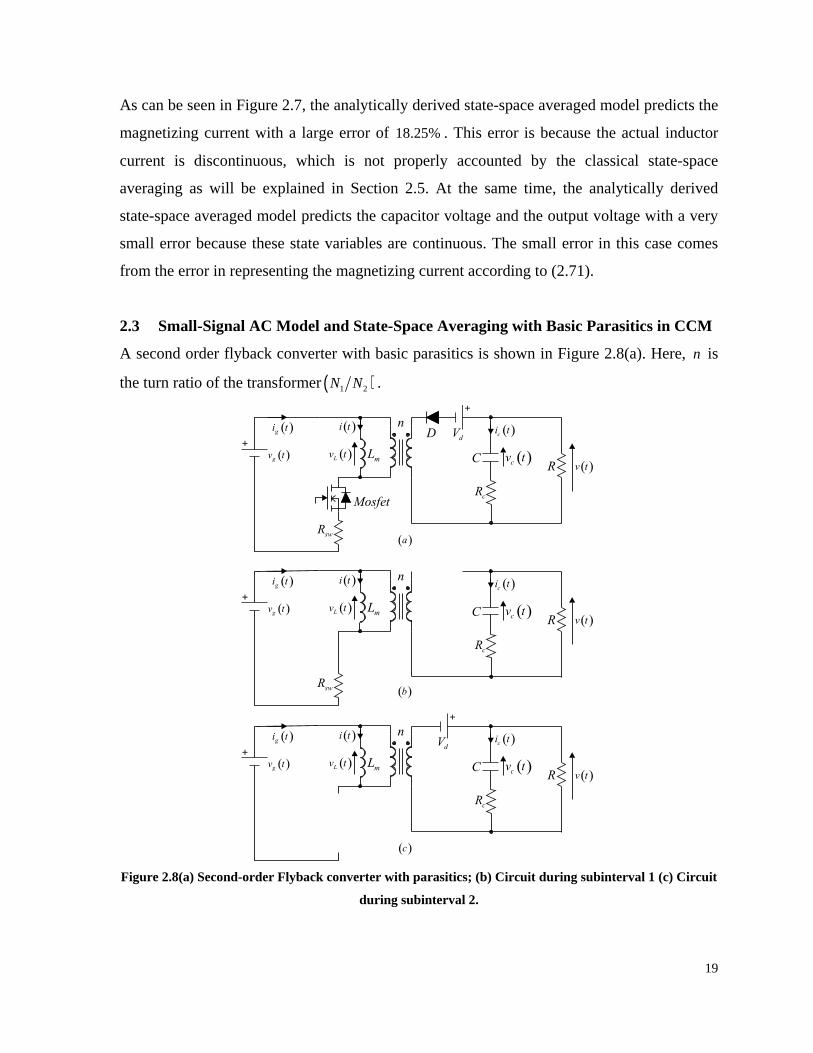
As can be seen in Figure 2.7, the analytically derived state-space averaged model predicts the
magnetizing current with a large error of 18.25%. This error is because the actual inductor
current is discontinuous, which is not properly accounted by the classical state-space
averaging as will be explained in Section 2.5. At the same time, the analytically derived
state-space averaged model predicts the capacitor voltage and the output voltage with a very
small error because these state variables are continuous. The small error in this case comes
from the error in representing the magnetizing current according to (2.71).
2.3 Small-Signal AC Model and State-Space Averaging with Basic Parasitics in CCM
A second order flyback converter with basic parasitics is shown in Figure 2.8(a). Here, n is
the turn ratio of the transformer( )1 2N N .
+
mL
n( )i t( )gi t ( )ci t
( )v t( )Lv t C
R
D
Mosfet
( )a
( )b
( )c
( )gv t
+
cR
swR
dV
( )cv t
+
mL
n( )i t( )gi t ( )ci t
( )v t( )Lv t C
R( )gv t
cR
swR
( )cv t
+
mL
n( )i t( )gi t ( )ci t
( )v t( )Lv t C
R( )gv t
+
cR
dV
( )cv t
Figure 2.8(a) Second-order Flyback converter with parasitics; (b) Circuit during subinterval 1 (c) Circuit
during subinterval 2.

20
During the first subinterval, when the MOSFET conducts and the diode is off, the circuit
reduces to Figure 2.8(b). For this interval, the inductor voltage ( )Lv t , capacitor current ( )ci t ,
converter output voltage( )v t , and converter input current ( )gi t are
( ) ( ) ( )L g sw gv t v t R i t= − (2.73)
( ) ( )cc
c
v ti t
R R= −
+ (2.74)
( ) ( )c
c
v t Rv t
R R=
+ (2.75)
( ) ( )gi t i t= (2.76)
We next apply the small ripple approximation and replace the voltages and currents with
their respective average values to obtain the following:
( ) ( ) ( )s s
L g sw gT Tv t v t R i t= − (2.77)
( )( )
sc T
cc
v ti t
R R= −
+ (2.78)
( )( )
sc T
c
v t Rv t
R R=
+ (2.79)
( ) ( )s
g Ti t i t= (2.80)
During the second subinterval, the MOSFET is off and diode conducts, which results in the
circuit of Figure 2.8(c). For this interval, the inductor voltage ( )Lv t , capacitor current ( )ci t ,
converter output voltage ( )v t , and converter input current ( )gi t are given by
( ) ( ) ( )( )L c c c dv t v t i t R V n= − − (2.81)
( ) ( ) ( )c
v ti t i t n
R
= − +
(2.82)
( ) ( ) ( )c c cv t v t i t R= − (2.83)
( ) 0gi t = (2.84)
Applying the small ripple approximation leads to the following:

21
( ) ( ) ( )s s
L c c c dT Tv t v t n i t R n V n= − − (2.85)
( ) ( )( )
s
s
T
c T
v ti t i t n
R= − − (2.86)
( ) ( ) ( )s s
c c cT Tv t v t i t R= − (2.87)
( ) 0gi t = (2.88)
The average inductor voltage now can be found by averaging the subintervals over one
complete switching period. The result is
( ) ( ) ( ) ( ) ( )
( ) ( ) ( ) ( ) ( )1 1
2 2 2
s s s
s s
L g sw gT T T
c c c dT T
v t v t d t R i t d t
v t nd t i t R nd t V nd t
= −
+ − − (2.89)
This leads to the following equation for the average inductor current
( )( ) ( ) ( ) ( )
( ) ( ) ( ) ( ) ( )1 1
2 2 2
s
s s
s s
Tm g sw gT T
c c c dT T
d i tL v t d t R i t d t
dt
v t nd t i t R nd t V nd t
= −
+ − − (2.90)
The average capacitor current now can be found by averaging the subintervals over one
switching period, which results in the following:
( )( )
( ) ( ) ( )( )
( )1 2 2s s
s s
c T T
c T Tc
v t v ti t d t i t nd t d t
R R R= − − −
+ (2.91)
This leads to the following equation for the average capacitor voltage
( ) ( )
( ) ( ) ( )( )
( )1 2 2s s s
s
c cT T T
Tc
d v t v t v tC d t i t nd t d t
dt R R R= − − −
+ (2.92)
The converter output voltage now can be found by averaging the subintervals over one
switching period, which results in
( )( )
( ) ( ) ( ) ( ) ( )1 2 2s
s s s
c T
c c cT T Tc
v t Rv t d t v t d t i t R d t
R R= + −
+ (2.93)
22
The converter input current can now be found by averaging the subintervals over one
switching period, resulting in the following:
( ) ( ) ( )1 0ss
g TTi t i t d t= + (2.94)
Equations (2.90), (2.92), (2.93), and (2.94) are nonlinear differential equations. Hence, to
construct the converter small-signal ac model, the next step is to perturb and linearize them.
We assume that the converter input voltage ( )gv t and duty cycle ( )1d t can be expressed as
quiescent values plus small ac variations, as follows
( ) ( )ˆs
g g gTv t V v t= + (2.95)
( ) ( )1 1 1ˆd t D d t= + (2.96)
In response to these inputs, and after all transients have decayed, the averaged converter
waveforms can be expressed as quiescent values plus small ac variations as
( ) ( )ˆs
g g gTi t I i t= + (2.97)
( ) ( )ˆsT
i t I i t= + (2.98)
( ) ( )ˆs
c c cTv t V v t= + (2.99)
( ) ( )ˆs
c c cTi t I i t= + (2.100)
( ) ( )ˆsT
v t V v t= + (2.101)
With these substitutions, the large-signal averaged inductor, (2.90), becomes
( )( ) ( )( ) ( )( ) ( )( ) ( )( )( )( ) ( )( ) ( )( ) ( )( )
( )( )
1 1 1 1
2 1 2 1
2 1
ˆˆ ˆˆˆ
ˆ ˆˆˆ
ˆ
m g g sw g g
c c c c c
d
d I i tL V v t D d t R I i t D d t
dt
V v t n D d t I i t R n D d t
V n D d t
+= + + − + +
+ + − − + −
− −
(2.102)
Upon multiplying this expression out and collecting terms, we obtain

23
( ) ( )
( ) ( ) ( ) ( ) ( )( ) ( ) ( ) ( )
1 1 2 2 2
1 1 1 1 1 1
2 1 2 1
1 ( )
ˆ
ˆ ˆ ˆˆˆ
ˆ ˆˆˆ
m g sw g c c c d
Dcterms
g g sw g sw g c
c c c c c d
st order acterms linear
di tdIL V D R I D V nD I R nD V nD
dt dt
V d t v t D R I d t R i t D V nd t
v t nD I R nd t i t R nD V nd t
+ = − + − −
+ − − − + + + − +
1444444442444444443
144444444 2
( ) ( ) ( ) ( ) ( ) ( )( ) ( ) ( )
1 1 1 1
1 1
2 ( )
ˆ ˆ ˆˆˆ ˆ
ˆ ˆˆ
g sw g c
c c d
nd order acterms nonlinear
v t d t R i t d t v t nd t
i t R nd t V nd t
− − + + +
444 444444444443
1444444442444444443
(2.103)
As usual, this equation contains three types of terms. The dc term contains no time-varying
quantities. The first order ac terms are linear functions of the ac variations in the circuit,
while the second order ac terms are functions of the products of the ac variations. At this
point, we make an assumption that the ac variations are small in magnitude compared to the
dc quiescent values,
( )( )( )
( )( )( )( )
1 1
ˆ
ˆ
ˆ
ˆ
ˆ
ˆ
ˆ
g g
g g
c c
c c
v t V
d t D
i t I
i t I
v t V
i t I
v t V
<<<<<<<<
<<
<<
<<
(2.104)
If the small signal assumptions (2.104) are satisfied, then the second-order terms are much
smaller in magnitude than the first-order terms and hence be neglected. The dc terms must
satisfy
1 1 2 2 20 g sw g c c c dV D R I D V nD I R nD V nD= − + − − (2.105)
The first order ac terms must satisfy
( ) ( ) ( ) ( ) ( ) ( )
( ) ( ) ( ) ( )1 1 1 1 1 1
2 1 2 1
ˆˆ ˆ ˆˆˆ
ˆ ˆˆˆ
m g g sw g sw g c
c c c c c d
di tL V d t v t D R I d t R i t D V nd t
dt
v t nD I R nd t i t R nD V nd t
= + − − −
+ + − + (2.106)
This is the linearized equation that describes ac variations in the inductor current.

24
Upon substation of (2.95)-(2.101) into (2.92), we obtain
( )( ) ( )( ) ( )( ) ( )( ) ( )( )( )( ) ( )( )
1 1 2 1
2 1
ˆ ˆ ˆ ˆˆ
ˆ ˆ
c c c c
c
d V v t V v tC D d t I i t n D d t
dt R R
V v tD d t
R
+ += − + − + −
+
+− −
(2.107)
Upon multiplying this expression out and collecting terms, we obtain
( )
( ) ( ) ( ) ( ) ( ) ( )
( ) ( ) ( ) ( ) ( )
1 22
1 1 1 21 2
1 ( )
11
ˆ
ˆ ˆˆ ˆˆ ˆ
ˆˆ ˆˆˆ
cc c
c
Dcterms
c c
c c
st order acterms linear
c
c
dv tdV V D VDC InD
dt dt R R R
V d t v t D Vd t v t DInd t i t nD
R R R R R R
v t d t v ti t nd t
R R
+ = − − − +
+ − − + − + − + +
+ − + ++
14444244443
144444444444424444444444443
( )1
2 ( )
ˆ
nd order acterms nonlinear
d t
R
14444444244444443
(2.108)
Here again we neglect the second-order terms. The dc terms of (2.108) must satisfy
1 220 c
c
V D VDInD
R R R= − − −
+ (2.109)
The first-order ac terms of (2.108) lead to the following small-signal for the ac capacitor
voltage
( ) ( ) ( ) ( ) ( ) ( ) ( )1 1 1 2
1 2
ˆ ˆˆ ˆ ˆˆ ˆc c c
c c
dv t V d t v t D Vd t v t DC Ind t i t nD
dt R R R R R R= − − + − + −
+ + (2.110)
Substation of (2.95)-(2.101) into (2.93) leads to
( )( ) ( )( ) ( )( ) ( )( ) ( )( )
( )( ) ( )( )1 1 2 1
2 1
ˆ ˆ ˆˆ ˆ
ˆˆ
c c
c cc
c c c
V v tV v t R D d t V v t D d t
R R
I i t R D d t
++ = + + + −
+
− + −
(2.111)
Upon multiplying this expression out and collecting terms, we obtain

25
( )( )
( ) ( ) ( ) ( )
( ) ( )
( ) ( ) ( ) ( ) ( ) ( )
12 2
1 11 2
1 2
1 ( )
11 1
ˆ
ˆ ˆ ˆ ˆ
ˆ ˆ
ˆˆ ˆ ˆˆˆ
cc c c
c
Dcterms
c cc c
c c
c c c c
st order acterms linear
cc c c
c
V D RV v t V D I R D
R R
V Rd t v t RDV d t v t D
R R R R
I R d t i t R D
v t Rd tv t d t i t R d t
R R
+ = + − +
+ − +
+ ++ + −
+ − + +
14444244443
1444444442444444443
2 ( )nd order acterms nonlinear
1444444442444444443
(2.112)
The dc term must satisfy
12 2
cc c c
c
V D RV V D I R D
R R= + −
+ (2.113)
We neglect the second-order terms in (2.112), leaving the following linearized ac equation
( ) ( ) ( ) ( ) ( ) ( ) ( )1 11 2 1 2
ˆ ˆ ˆ ˆ ˆˆ ˆc cc c c c c c
c c
V Rd t v t RDv t V d t v t D I R d t i t R D
R R R R= + − + + −
+ + (2.114)
Substation of (2.95)-(2.101) into (2.94) leads to
( ) ( )( ) ( )( )1 1ˆˆ ˆ
g gI i t I i t D d t+ = + + (2.115)
Upon multiplying this expression out and collecting terms, we obtain
( ) ( )
( ) ( )( ) ( ) ( )( )1 1 1 1
1 ( ) 2 ( )
ˆ ˆˆ ˆ ˆg g
Dctermsst order acterms linear nd order acterms nonlinear
I i t ID Id t i t D i t d t+ = + + +1442443 14243
(2.116)
The dc term must satisfy
1gI ID= (2.117)
We neglect the second-order terms in (2.116), leaving the following linearized ac equation
( ) ( ) ( )1 1ˆˆ ˆ
gi t Id t i t D= + (2.118)
This result represents the low-frequency ac variations in the converter input current.
The equations of the quiescent values, (2.105), (2.109), (2.113), and (2.117) are collected
below as

26
1 1 2 2 2
1 22
12 2
1
0
0
g sw g c c c d
c
c
cc c c
c
g
V D R I D V nD I R nD V nD
V D VDInD
R R R
V D RV V D I R D
R R
I ID
= − + − − = − − −+ = + −+
=
(2.119)
For given quiescent values of the input voltage gV , the diode voltage drop dV , and the duty
cycle 1D , the system (2.119) can be evaluated to find the quiescent output voltage V ,
inductor current I , input current gI , capacitor voltage cV , and capacitor current cI .
However, in this problem there are 5 variables but there are only 4 equations. The fifth
equation can be the following
c c cV V I R= − (2.120)
The results are then inserted into the small-signal ac model.
The small signal ac model, (2.106), (2.110), (2.114), and (2.118), is summarized below
( ) ( ) ( ) ( ) ( ) ( )
( ) ( ) ( ) ( )( ) ( ) ( ) ( ) ( ) ( ) ( )
( ) ( ) ( ) ( ) ( ) ( )
1 1 1 1 1 1
2 1 2 1
1 1 1 21 2
1 11 2 1
ˆˆ ˆ ˆˆˆ
ˆ ˆˆˆ
ˆ ˆˆ ˆ ˆˆ ˆ
ˆ ˆ ˆ ˆ ˆˆ ˆ
m g g sw g sw g c
c c c c c d
c c c
c c
c cc c c c c
c c
di tL V d t v t D R I d t R i t D V nd t
dt
v t nD I R nd t i t R nD V nd t
dv t V d t v t D Vd t v t DC Ind t i t nD
dt R R R R R R
V Rd t v t RDv t V d t v t D I R d t i
R R R R
= + − − −
+ + − +
= − − + − + −+ +
= + − + + −+ +
( )
( ) ( ) ( )
2
1 1ˆˆ ˆ
c
g
t R D
i t Id t i t D
= +
(2.121)
The final step is to construct an equivalent circuit of (2.119) and(2.121) using the
commercially available simulation tools.
27
Let us now apply the state-space averaging method to the second order flyback converter of
Figure 2.8(a). The independent state variables as usual are the inductor current ( )i t and the
capacitor voltage ( )cv t , which form the state vector
( ) ( )( )c
i tx t
v t
=
(2.122)
The input voltage ( )gv t , and the diode voltage drop is an independent source, which should
be placed in the input vector as
( ) ( )g
d
v tu t
V
=
(2.123)
To model the converter input port and output port, we need to find the converter input current
( )gi t and output voltage ( )v t . To calculate this dependent current and voltage, it should be
included in the output vector ( )y t as
( ) ( )( )
gi ty t
v t
=
(2.124)
Next, let us write the state equations for each subinterval. When the switch is on and the
diode is off, the converter circuit of Figure 2.8(b) is obtained. The inductor voltage, capacitor
current, output voltage, and converter input current are
( ) ( ) ( )m g sw
di tL v t R i t
dt= − (2.125)
( ) ( )c c
c
dv t v tC
dt R R= −
+ (2.126)
( ) ( )c
c
v t Rv t
R R=
+ (2.127)
( ) ( )gi t i t= (2.128)
Similar to (2.73)-(2.76), after organizing the terms in (2.125)-(2.128), the result can be
written in the following state-space form

28
( )
( )
( )
( )( )( )
( )
( )1
1
0 10
10 0 0
sw
m gm
c dc
u tx tcB
dx t A
dt
Rdi tL i t v tdt L
v t Vdv tRC R Cdt
− = + − +
1424312314243
14243 144424443
(2.129)
( )( )( )
( )( )( )
( )
( )1
1
1 00 0
0 0 0g g
c dc
E u ty t x tC
i t i t v tR
v t v t VR R
= + + 12314243123 123
1442443
(2.130)
So the state-space equations for the first subinterval have been identified.
In the second subinterval, when the MOSFET is off and the diode is on, the converter circuit
of Figure 2.8(c) is obtained. For the second subinterval, the inductor voltage, capacitor
current, output voltage, and converter input current are given by
( ) ( ) ( )2
c cm d
c c
di t i t n R R v t nRL V n
dt R R R R= + −
− − (2.131)
( ) ( ) ( )c c
c c
dv t i t nR v tC
dt R R R R= − −
− − (2.132)
( ) ( ) ( )c c
c c
i t nR R v t Rv t
R R R R= +
− − (2.133)
( ) 0gi t = (2.134)
After organizing them and writing in state-space form, we get
( )
( )
( )
( )( )( )
( )
( )2
2
2
0
10 0
c
gm c m m c mm
c dc
u tx tc cB
dx t Adt
n R R nRdi tn
i t v tRL R L RL R Ldt Lv t VnRdv t
RC R C RC R Cdt
− − − = + − − − −
1424312314243
14243 1444442444443
(2.135)

29
( )( )( )
( )( )( )
( )
( )2
2
0 00 0
0 0g g
cc d
c cE u ty t x t
C
i t i t v tnR R R
v t v t VR R R R
= + − − 12314243123 123
144424443
(2.136)
So the space-space equation of the second interval has also been identified.
The next step is to combine the result and obtain the state-space averaged model as
2
1 1 2 2 1 2
21 2 2
2 1 2
0
1 10
sw c
m m c m m c m
c c c
sw c
m m c m m c m
c c c
R n R R nRL RL R L RL R L
A A D A D D DnR
RC R C RC R C RC R C
R D n R RD nRD
L RL R L RL R L
nRD D D
RC R C RC R C RC R C
− − − = + = +
− − − + − −
− + − − =
− − − − + −
(2.137)
1 2
1 1 2 2 1 2
10 0
0 0 0 0 0 0m m m m
D nDn
L L L LB B D B D D D
− − = + = + =
(2.138)
1 1 2 2 1 2
1
2 1 2
0 01 0
0
0
c
c c c
c
c c c
C C D C D D DnR RR R
R R R R R R
D
nR RD RD RD
R R R R R R
= + = +
+ − −
= + − + −
(2.139)
1 1 2 2 1 2
0 0 0 0 0 0
0 0 0 0 0 0E E D E D D D
= + = + =
(2.140)
Therefore, the final state-space averaged model of the second order flyback converter with
parasitics in CCM becomes

30
( )
( )( )( )
( )
21 2 2
2 1 2
1 2
0 0
sw c
m m c m m c m
cc
c c c
gm m
d
R D n R RD nRDdi ti tL RL R L RL R Ldtv tnRD D Ddv t
RC R C RC R C RC R Cdt
D nDv t
L LV
− + − − = − − − − + −
− +
(2.141)
( )( )
( )( )
( )1
2 1 2
00 0
0 0g g
cc d
c c c
Di t i t v t
nR RD RD RDv t v t V
R R R R R R
= + + − + −
(2.142)
To validate the analytically derived state-space averaged model in CCM, a detailed model of
Figure 2.8(a) has been constructed in PLECS [16]. The state-space averaged model has been
constructed in Matlab/Simulink [30]. The same hardware prototype has been used here to
validate the results. The parameters of the second-order flyback converter with basic
parasitics in CCM are given in Appendix A.3. The predicted and measured inductor current,
capacitor voltage, and output voltage are shown in Figure 2.9.
As can be seen in Figure 2.9, the analytically derived state-space averaged model predicts the
averaged inductor current and capacitor voltage very well. There is a difference between the
detailed model and hardware prototype in terms of the output voltage (see Figure 2.9), which
comes from the simplified detailed model (second-order with parasitics). As seen in Figure
2.10, the analytically derived state-space averaged model predicts the average output voltage
very well.

31
0.5
1
1.5
I (A
mp
.)
-72.496
-72.492
-72.488
Vc (
Vo
lt)
0.999991 0.999993 0.999995 0.999997
-72.6
-72.2
-71.8
-71.4
Time (s)
V (
Vo
lt)
Actual Average andAnalytical State-Space
SeeFigure 2.10
Detailed Model
Actual Average
Analytical State-Space
Detailed Model
Actual Average
Analytical State-Space
Hardware Prototype
Figure 2.9 Inductor current, capacitor voltage and output voltage of second order Flyback converter with
parasitics in CCM.
0.999991 0.999993 0.999995 0.999997
-72.5
-72.495
-72.49
-72.485
-72.48
Time (s)
V (
Volt)
Detailed Model
Actual Average
Analytical State-Space
Figure 2.10 Output voltage of second order Flyback converter with parasitics in CCM.

32
2.4 State-Space Averaging with Parasitics in DCM
In addition to the two subintervals that occur in CCM, here there is another subinterval that
occurs at light loads. The topology of the flyback converter in this subinterval is shown in
Figure 2.11.
+
mL
n( )i t( )gi t ( )ci t
( )v t( )Lv t C
R( )gv t
cR
( )cv t
Figure 2.11 Second-order Flyback converter with parasitics during third subinterval in DCM.
During the first subinterval depicted in Figure 2.8(b), the MOSFET is on and the diode is off,
and the magnetizing inductance stores some energy. During the second subinterval depicted
in Figure 2.8(c), the MOSFET is off and the diode is on. During this interval, the stored
energy is transferred to secondary side and it flows through the filter capacitor to the load
resistor. If the magnetizing current during the second interval goes to zero before the end of
the second interval, the converter goes to another stage resulting in third subinterval and
DCM, before it goes back to the first interval in the next cycle.
For the flyback converter without parasitics in DCM, the first and second sub intervals
remain of the same as in CCM as described in Section 2.3. The third interval comes into
account when the MOSFET and the diode are off as in Figure 2.11. For this case, the
inductor voltage ( )Lv t , capacitor current ( )ci t , output voltage ( )v t , and converter input
current ( )gi t are
( ) 0Lv t = (2.143)
( ) ( )cc
c
v ti t
R R= −
+ (2.144)
( ) ( )c
c
v t Rv t
R R=
+ (2.145)

33
( ) 0gi t = (2.146)
Let us now apply the state-space averaging method to the third interval of Figure 2.11. The
inductor voltage, capacitor current, output voltage, and converter input current can be written
as
( )
0m
di tL
dt= (2.147)
( ) ( )c c
c
dv t v tC
dt R R= −
+ (2.148)
( ) ( )c
c
v t Rv t
R R=
+ (2.149)
( ) 0gi t = (2.150)
Similar to (2.143)-(2.146), after organizing terms in (2.147)-(2.150), these equations can be
written as
( )
( )
( )
( )( )( )
( )
( )3
3
0 00 0
10 0 0
g
c dcc
B u tx tA
dx t
dt
di ti t v tdtv t Vdv t
RC R Cdt
= + − +
12314243123
14442444314243
(2.151)
( )( )( )
( )( )( )
( )
( )3
3
0 00 0
0 0 0g g
c dc
E u ty t x tC
i t i t v tR
v t v t VR R
= + + 12314243123 123
1442443
(2.152)
which defines the state-space equation for the third subinterval. Hence, the next step is to
evaluate the state-space averaged equations, which goes as following:

34
1 1 2 2 3 3
2
1 2 3
21 2 2
1 32 2
0 0 0
101 1
0
sw c
m m c m m c m
cc c c
sw c
m m c m m c m
c c c
A A D A D A D
R n R R nRL RL R L RL R L
D D DnR
RC R CRC R C RC R C RC R C
R D n R RD nRD
L RL R L RL R L
D DnRD D
RC R C RC R C RC R C
= + +
− − − = + + −
− +− − + − −
− + − −= +− − −
− + −
(2.153)
1 2
1 1 2 2 3 3 1 2 3
10 0 0 0
0 00 0 0 0 0 0m m m m
D nDn
L L L LB B D B D B D D D D
− − = + + = + + =
(2.154)
( )
1 1 2 2 3 3 1 2 3
1
1 32 2
0 01 0 0 0
0 0
0
c
c cc c
c
c c c
C C D C D C D D D DnR RR RR
R R R RR R R R
D
R D DnR RD RD
R R R R R R
= + + = + +
+ + − −
= + + − + −
(2.155)
1 1 2 2 3 3 1 2 3
0 0 0 0 0 0 0 0
0 0 0 0 0 0 0 0E E D E D E D D D D
= + + = + + =
(2.156)
The final state-space averaged model for the second order flyback converter with parasitics
in DCM becomes:
( )
( )( )( )
( )
21 2 2
1 32 2
1 2
0 0
sw c
m m c m m c m
cc
c c c
gm m
d
R D n R RD nRDdi ti tL RL R L RL R Ldtv tD DnRD Ddv t
RC R C RC R C RC R Cdt
D nDv t
L LV
− + − − = + − − − − + −
− +
(2.157)
( )( ) ( ) ( )
( )( )1
1 32 2
00 0
0 0g g
cc d
c c c
Di t i t v t
R D DnR RD RDv t v t V
R R R R R R
= ++ + − + −
(2.158)

35
To validate the analytically derived state-space averaged model in DCM, a detailed model of
the converter circuit depicted Figure 2.8(a) has been constructed in PLECS [16]. The state-
space averaged model has been constructed in Matlab/Simulink [30].The variable 2d has
been calculated using (2.58) and set to 0.4409. The load was assumed as 2500LR R= = Ω .
The parameters of the second-order flyback converter without parasitics in CCM are given in
Appendix A.4. The predicted inductor current and capacitor voltage are shown in Figure
2.12.
0
0.5
1
I (A
mp.)
-102
-101.5
-101
Vc (
Volt)
0.999991 0.999993 0.999995 0.999997-102
-101.5
-101
Time (s)
V (
Volt)
Detailed Model
Actual Average
Analytical State-SpaceDetailed Model and
Actual Average
Detailed Model andActual Average
Figure 2.12 Inductor current, capacitor voltage and output voltage of second order Flyback converter
with parasitics in DCM.
As can be seen in Figure 2.12, the analytically derived state-space averaged model predicts
the magnetizing current with a large error of 17.5%. This error is because the current is
discontinuous, while the conventional state-space averaging fails to correctly take this into

36
account. At the same time, the analytically derived state-space averaged model predicts the
capacitor voltage with a very small error because the capacitor voltage is a continuous state
variable. The small error comes from the error in the magnetizing current defined by (2.157).
2.5 Parametric Average Value Modeling in CCM and DCM
To see the challenges with the conventional state-space averaging in DCM and representation
of parasitics, we take another detailed look at this approach. The state-space averaging is a
well defined approach [18] that has been presented previously in numerous publications, e.g.
[8, 10, 33]. In CCM, the state-space equation is
( ) ( ) ( )( )( ) ( ) ( ) ( )( )( ) ( )1 2 1 21 1x t q t A q t A x t q t B q t B u t•
= + − + + − (2.159)
where ( )q t is the switching function, ,k kA B are the system matrices, and ( )u t is the input
vector. By definition, the so-called fast average of a state variable ( )x t over a switching
interval is
( ) ( )1 st T
s t
x t x t dtT
+
= ∫ (2.160)
where ( )x t is the actual or the true average of ( )x t . Since the averaging is commutative
with respect to differentiation, taking the fast average of (2.159) over a switching interval
yields
( ) ( ) ( )( )( ) ( ) ( ) ( )( )( ) ( )1 2 1 21 1x t d t A d t A x t d t B d t B u t•
= + − + + − (2.161)
This result follows from the fact that the fast average of the switching function over a
switching interval is the duty cycle function
( ) ( )1 st T
s t
d t q t dtT
+
= ∫ (2.162)
It is also assumed that the average of the product is equal to the product of the averages,
especially
Ax A x= ⋅ (2.163)
Bu B u= ⋅ (2.164)
Assumption (2.163) is acceptable if the original switching variables do not deviate
significantly from their average values and also the system matrices 1A and 2A are

37
commutative [18, 34]. But in general, the matrices 1A and 2A are not commutative [35, 36].
So, if we make assumption (2.163), the equation (2.161) is not an exact solution as
mentioned in [18] and Appendix A, but can only be an approximation. Assumption (2.164) is
usually accepted when the source ripple is neglected.
The DCM operation of PWM converters differs from CCM operation by an additional time
interval in each switching cycle during which the inductor current or capacitor voltage is
clamped to zero (or a constant when there are multiple energy storage elements).
Conventional state-space averaging for converters working in DCM has been summarized in
[4, 10, 18]. For this mode, the direct extension of (2.159)-(2.161) results in
( ) ( ) ( ) ( ) ( )1 1 2 2 3 3 1 1 2 2 3 3x t d A d A d A x t d B d B d B u t•
= + + + + + (2.165)
which is no longer accurate. In particular, the local average of the magnetizing current in the
third interval is zero, whereas the state-space averaging implies that this value should be 3d i .
Since 3d and i are not zero, the result of the state-space averaging is not zero. That is why
the discontinuous averaged variable in DCM is higher than the actual averaged value that can
be seen in Figure 2.7 and Figure 2.12.
As shown in Sections 2.2 and 2.4, the conventional state-space averaging is no longer
accurate in DCM. The parametric average-value modeling has been proposed to solve this
problem as documented in numerous publications [22, 24-27].
2.5.1 Correction Term
The state-space averaging involves the weighted sum of the state-space equations
corresponding to different topological instances within a switching interval. In DCM, a
prototypical switching interval is divided into three subintervals as seen in Figure 2.6. To
accurately represent the dynamics of the underlying converter circuit, a corrected full order
state-space averaged model [4] has been proposed for an ideal converter circuit as
( )3 3
1 1k k k k
k k
x d A Mx d B u•
= =
= + ∑ ∑ (2.166)

38
To make state-space averaging work properly in DCM, the so-called correction matrix M is
added in (2.166). The analytical derivation of the correction matrix for an ideal topology
(without parasitics) is given in [4]. Since the circuit of Figure 2.8(a) with parasitics has been
considered in this study, it would be very complicated to extend that analytical solution.
Hence, a numerical solution has been adopted in this Thesis.
The correction term is a diagonal matrix, wherein each state variable has its own correction
coefficient. In this implementation presented in this Thesis, instead of a diagonal matrix, a
column correction vector (each state variable has its own correction term as an element of
column matrix) is proposed as
( ) ( )3 3
1 1
.k k k kk k
x d A x M d B u•
= =
= ∗ + ∑ ∑ (2.167)
where ( ).x M∗ denotes the element wise multiplication. This operation uses less
computational time compare to direct implementation of (2.166).
2.5.2 Model Implementation
A detailed model of the converter depicted in Figure 2.8(a) has been constructed using the
PLECS toolbox. The system matrices ( ), , ,k k k kA B C D in each subinterval can be extracted
numerically using PLECS and Simulink built-in feature for numerical model linearization
and analysis. Since the detailed model includes all the parasitics, the extracted system
matrices will have all the necessary information in them by construction and without any
extra analytical derivations. The elements of correction vector ( )M and ( )3d are obtained as
functions of the duty-cycle ( )1d and the average value of the state variables ( )x . To obtain
the values of ( )3 1,d d x and ( )1,M d x , the detailed model is run in the operation region of
interest (for example; duty-cycle changes between 0.1 and 0.9, and the load ( )R changes
from very low load to very high load) whereas the state variables are averaged numerically
over the prototyping switching interval and saved for the future use. In particular, the
average-value of the state vector ( )x is computed in a steady-state corresponding to a given
operation point. Specifically, in steady-state we have

39
( ) ( )3 3
1 1
0 .k k k kk k
d A x M d B u= =
= ∗ + ∑ ∑ (2.168)
From which an intermediate variable vector p is computed as
( ) ( )13 3
1 1
. k k k kk k
p x M d A d B u−
= =
= ∗ = − ⋅ ∑ ∑ (2.169)
Thereafter the elements of M can be found using the following
j j jM p x= ⋅ ÷ (2.170)
where j denotes number of state variables and ( )j jp x⋅ ÷ denotes element wise division.
To obtain the functions ( )3 1,d d x and ( )1,M d x for the desired operation range, the detailed
simulation is run with different values of control variable ( )1d as well as the load( )R . The
variables resulting from this procedures are 1 2 3, , , , ,cd d d R v i and the correction vector ( )M is
computed using (2.169) and (2.170). These variables are stored for future use in lookup
tables, wherein an interpolation/extrapolation may be used as necessary. The real challenge
here is to calculate the 2d or 3d at any given operation point. If one can calculate either one,
thereafter it becomes easy to calculate the other one since 1d is the control variable which
can be calculated from the magnetizing current. As can be seen in Figure 2.12, the
magnetizing current is zero during the third subinterval whereas the variable 3d can be
calculated.
The final numerical function for 3d is plotted in Figure 2.13, which shows that this function
has a flat surface corresponding to CCM, and varies linearly along the 1d . In DCM, the
surface of 3d becomes non-linear and increases.

40
01000
20003000
40005000
0.10.20.30.40.50.60.70.80.91
0
0.1
0.2
0.3
0.4
0.5
0.6
0.7
R (ohm)
d1
d3
CCM
DCM
Figure 2.13 Variable 3d as a function` of duty-cycle ( )1d and the load ( )R .
The correction term ( )1m of the magnetizing current ( )I is plotted in Figure 2.14 as a
function of duty-cycle ( )1d and the load resistance ( )R . As can be seen in Figure 2.14, on
the one hand, the correction term ( )1m has a flat surface and value of 1 in CCM, which
implies that the state-space averaging captures the correct value of this current in CCM and
no correction is required. On the other hand, it has values higher than 1 corresponding to the
DCM because the conventional state-space averaging does not capture the correct average
values in this region of operation as explained in Section 2.5, and therefore the correction
effort is required.
01000
20003000
40005000
0.10.20.30.40.50.60.70.80.910.8
1
1.2
1.4
1.6
1.8
2
2.2
2.4
2.6
R (ohm)
d1
m1
CCM
DCM
Figure 2.14 The correction term 1m as a function of duty-cycle ( )1d and the load resistance ( )R .

41
The correction term ( )2m of filter capacitor voltage ( )cv is plotted in Figure 2.15 as a
function of the duty-cycle( )1d and the load resistance ( )R . As can be seen in Figure 2.15,
the calculated value for this correction term is 1 for either CCM or DCM. This value is
consistent with the fact that the capacitor voltage is a continuous state variable with relatively
small ripple, so the conventional state-space averaging predicts the correct average value for
this variable for both modes.
01000
20003000
40005000
0.10.20.30.40.50.60.70.80.91
0.98
0.99
1
1.01
1.02
R (ohm)
d1
m2
CCM and DCM
Figure 2.15 The correction term 2m as a function of duty-cycle ( )1d and the load resistance ( )R .
Once the parametric functions ( )3 1,d d x and ( )1,M d x have been calculated and stored, these
functions become available for the model implementation. Finally, the parametric average-
value model is implemented according to the block diagram shown in Figure 2.16. The
system matrices ( ), , ,k k k kA B C D for each subinterval are calculated numerically. For a given
value of control variable 1d and state vector x , the values of 3d and correction vector ( )M
are acquired through the lookup tables. Total average system matrices ( ), , ,T T T TA B C D are
computed using the system matrices ( ), , ,k k k kA B C D and the variables 1 2,d d and 3d . These
matrices are then used to build the new continuous non-linear state-space average-value
model that replaces the discontinuous detailed model. Thereafter, this parametric average-
value model can be used for large-signal transient studies as well as for numerical
linearization and subsequent small-signal frequency-domain analysis.

42
3d
M
x
1d
u
y
( )
( )
( )
( )
2 1 3
3
1
3
1
3
1
3
1
1
T k k
k
T k k
k
T k k
k
T k k
k
d d d
A d A
B d B
C d C
D d D
=
=
=
=
= - -
=
=
=
=
å
å
å
å
( )T T
T T
x A x M B u
y C x D u
·
= ×* +
= +
, , ,k k k kA B C D
( )
( )3 1
1
,
,
d d x
M d x
Figure 2.16 Implementation of the parametric average-value model.
The previously proposed parametric average-value models [24-27] had problem with the
correcting the output equation. In particular, in the previous formulation the output equation
was defined as
( )3 3
1 1k k k k
k k
y d C Mx d D u= =
= + ∑ ∑ (2.171)
However, my simulation results (which are not shown in this study) have shown that if there
is a correction term ( )M in the output equation, in this case no correction occurs on the
output voltage ( )V . The reason for this is that the state vector ( )x has already been corrected
in the state equation (2.167), and therefore no additional correction is required in the output
equation. The analytical proof of this argument goes as follow:
During the steady-state, we have
1 10 T T T TA Mx B u x M A B u− −= + ⇒ = − (2.172)
When (2.172) is inserted into (2.171), the output equation becomes
( )1 1T T T Ty C M M A B u D u− −= − + (2.173)
After required calculations in (2.173), we get
1T T T Ty C A B u D u−= − + (2.174)
If there is a correction term in (2.171), there is no correction occurs in (2.174). Therefore, the
correct output equation is

43
( )3 3
1 1k k k k
k k
y d C x d D u= =
= + ∑ ∑ (2.175)
2.5.3 Case Studies
The flyback converter shown in Figure 2.8(a) is used here for the case studies. The detailed
model has been implemented using PLECS. The converters parameters are summarized in
the Appendices A.3 and A.4 for CCM and DCM, respectively. The proposed parametric
average-value model has been implemented and compared to the hardware prototype, the
detailed model and the conventional state-space averaging model in both time and frequency
domains.
2.5.3.1 Time domain
To demonstrate the parametric average-value model (PAVM) in DCM, the system is operates
in steady-state defined by 1 0.381d = and 2500R= Ω . The resulting simulated waveforms of
the magnetizing current, filter capacitor voltage and the output voltage are plotted in Figure
2.17. As can be seen in Figure 2.17, the PAVM predicts the average-value of the steady state
waveforms in DCM very well compared to the conventional state-space averaging. Actual
average of the inductor current is 0.46Amp, and the PAVM can predict this value very well.
On the other hand, the analytical state-space averaging can predict this value as
0.55 .Amp which is equal to 18.18% error. Actual average of the capacitor voltage is
101.56V− , and the PAVM can predict this value very well. The analytical state-space
averaging can predict this value as 101.2V− .

44
0
0.5
1
I (A
mp
.)
-102
-101.5
-101
Vc (
Vo
lt)
0.999991 0.999993 0.999995 0.999997-102
-101.5
-101
Time (s)
V (
Vo
lt)
Detailed Model,Actual Average
and PAVM
Detailed Model
Actual Average
Analytical State-Space
PAVM
Actual Averageand PAVM
Detailed Model,Actual Average
and PAVM
Figure 2.17 Simulated inductor current, capacitor voltage and output voltage of the second order Flyback
converter with parasitics in DCM.
The accuracy of the PAVM in predicting the large-signal behaviour in time-domain has also
been verified by studying the effect of sudden change in load. In the following study, the
output of the flyback converter was regulated using a PI controller. The PI controller was
designed to regulate the output voltage at 72V− by adjusting the duty-cycle ( )1d . The
controller parameters are 0.7pK = and 25iK = . In this study, the converter run with a
resistive load of 2000Ω (which results in DCM) until it reaches a steady-state. At 0.2t s= , a
parallel load of 500Ω is added (which results in CCM). The resulting time-domain transients
are shown in Figure 2.18.

45
0
1
2
3
I (A
mp.)
-72
-71.8
-71.6
Vc
(Volt)
0.1996 0.1998 0.2 0.2002 0.2004 0.2006 0.2008 0.201
-72
-71.8
-71.6
Time (s)
V (
Volt)
PAVM
Detailed Model
Detailed Modeland PAVM
Detailed Modeland PAVM
Figure 2.18 Transients in inductor current, capacitor voltage and output voltage of the second order
Flyback converter due to the step change in load.
As it can be observed in Figure 2.17, after the load change at 0.2t s= , the converter switches
operation from DCM to CCM. After load changes the control action brings the output
voltage to about the desired 72V− after about 0.15s which wasn't shown in Figure 2.18 to
demonstrate the response of the PAVM to load change. At the same time, as it can be seen in
Figure 2.17, through all transients the large signal behaviour of the detailed model is
accurately predicted by proposed PAVM.
2.5.3.2 Frequency domain
The control-to-output transfer function is often considered in literature for verifying the
small-signal behaviour of the converter models. The small-signal injection and subsequent
frequency sweep method has been implemented to extract the small-signal transfer function

46
from the detailed simulation and the PAVM corresponding to full load operation condition
defined by 717.05R= Ω and 1 0.381d = . The magnitude and phase of the corresponding
control-to-output transfer function are plotted in Figure 2.19.
The transfer function is evaluated up to150kHz, which is more than one-half of the switching
frequency( )250kHz . Closer to the switching frequency the results become distorted due to the
interaction between the injected perturbations and the converter switching. In general,
considering the frequencies closer to and above the switching frequency has limited use for
the average-value model since the basic assumptions of the averaging are no longer valid.
-20
-10
0
10
20
30
Am
plit
ude (
dB
)
102
103
104
105
-90
-80
-70
-60
-50
-40
-30
-20
-10
0
Phase (
°)
Frequency (Hz)
PAVM
Detailed
PAVM
Detailed
Figure 2.19 Control-to-output transfer function of the second-order Flyback converter evaluated at
717.05R= Ω and 1 0.381d = .

47
Chapter 3 : Analysis of Flyback Converter with Snubber Circuits
Real semiconductor devices experience voltage and current stress during the turn-on and
turn-off transitions which can easily damage the circuit elements. If a power electronic
converter stresses a power semiconductor device beyond its ratings, there are two basic ways
of relieving the problem. Either the device can be replaced with one whose ratings exceed the
stresses, or a snubber circuits can be added to the converter in order to reduce the stress to
safe levels. The final choice always involves a trade-off between the cost and availability of
semiconductor devices with required electrical ratings compared to the cost and additional
complexity of using the snubber circuits [9, 37-40]. In some topologies, such as a transformer
isolated Flyback converter, the snubber circuit may be required to protect the switching
transistor due to non-zero transformer leakage inductance.
3.1 Fifth –order Flyback Converter with Snubbers
The circuit with snubbers considered in this Chapter is shown in Figure 3.1. Also, a hardware
prototype that has been built includes the snubbers. The parameters and the detailed circuit
diagram are given in Appendices A.5 and Appendix B, respectively. The circuit is has fifth-
order because it has a high order transformer model with primary and secondary leakage
inductances, and two RCsnubber circuits ( ),ss ss ds dsC R C R− − to protect the MOSFET and
diode during turn-on and turn-off switching transitions.
+
+
sL
mL
R
cR
ssR
dsR
swR
C
dsC
ssC
gV
Mosfet
V
dVDn
pL
Figure 3.1 Fifth-order Flyback converter circuit.

48
To demonstrate the role and effect of the snubber circuit, the measured transformer
secondary voltage waveforms with and without the diode snubber is shown in Figure 3.2.
-100
0
100
200
300
Vs
(Volt)
5.983 5.984 5.985 5.986 5.987 5.988 5.989
x10-3Time (s)
-100
0
100
200
300
Vs
(Volt)
( )a
( )b
Figure 3.2 Measured transformer secondary voltage: (a) without the diode snubber; and (b) with the
diode snubber.
As can be seen in Figure 3.2(a), when the snubber is not used on the secondary side, the
voltage spikes up to 310V and the oscillations die pretty much at the end of the switching
interval. This phenomena causes two problems. First, the spike voltage can cause
breakdowns on the switching device. Secondly, the ringing energy will be radiated creating
noise and electro-magnetic interference (EMI) issues with potential for logic and control
errors. This type of ringing is not acceptable and it is necessary to add the snubber circuit
elements to damp the ringing, or clamp the voltage (with RCD clamps), or active snubbers
[40]. In the hardware prototype, a conventional RC snubber is used because of its simplicity
and low part count. Calculation of the RC elements is not the interest of this Thesis, whereas
the reader can find more information in [9, 37-39].

49
It must be emphasized that the snubbers are not a fundamental part of a power electronic
converter circuit. However, when it comes to averaging of PWM converters, the snubbers
significantly add to the complexity of the problem, and to the best of our knowledge this has
not been considered in the prior literature. At the same time, since the snubber circuits have
an important role in overall system dynamics, it is very desirable to take them into account in
the average-value modeling. On the one hand, the benefit of considering the snubbers will be
the improved accuracy of the average model in terms of capturing and predicting the
converter losses and efficiency, which will be used in Section 4.4.3. On the other hand, their
presence in the circuit has introduced more complexity and theoretical problems which are
almost impossible or impractical to resolve using conventional analytical derivations of the
average-value models as will be explained in more detail in Section 3.2.
3.2 State-Space Averaging Phenomena with the Snubbers
The circuit considered in this Section is shown in Figure 3.1. This circuit is a fifth-order
system which makes it more difficult to derive state equations analytically. A more practical
method to calculate the state-space equation is to built a detailed switching model using any
commercially available software programs and extract the state-space matrices numerically
from the detailed model [16, 30] for each subinterval. These matrices can then be used for the
state-space averaging.
A detailed analysis of the fifth-order Flyback converter will be given in Chapter 4. In this
Section, we will focus on only the problem caused by the snubbers, not the whole converter
circuit. The problem occurs on the output filter capacitor voltage, which also translates to the
output voltage which has been defined as an output in state-space output equation. To
demonstrate this problem caused by the snubbers, a detailed model has been built using
PLECS [16]. The corresponding converter parameters are summarized in Appendix A.5. The
state matrices , , ,k k k kA B C D have been extracted for each subinterval in CCM. Finally, the
state-space averaged model has been calculated using these matrices and given duty ratio.
The simulated output filter capacitor voltage and the output voltage are shown Figure 3.3.

50
0.0499 0.04991 0.04992 0.04993
-80
-60
-40
-20
0
Time (s)
V (
Vo
lt)
Detailed Model
Actual Average
State-Space Averaging
c
-80
-60
-40
-20
0
V (
Vo
lt)
Detailed Modeland Actual Average
Detailed Modeland Actual Average
Figure 3.3 Simulated output filter capacitor voltage and the output voltage of the fifth-order Flyback
converter with snubbers in CCM.
As can be seen in Figure 3.3, the output voltage and capacitor voltage is about 72V− , which
corresponds to the considered operating point in CCM. However, the state-space averaged
predicts the very low value of about1.25V− . Since the output voltage and the capacitor
voltage are continuous and slow variables, the conventional state-space averaging should
predict the average value correctly but in this can it does not! The reason why this is
happening can be understood by examining the Figure 3.1. The output filter capacitor voltage
is created by the charging current that flows through the diode. On the one hand, if the
average current is predicted correctly, the capacitor voltage will also be correct. But on the
other hand, if we look at the final state-space averaged equation (3.1), the extracted from the
detailed model diode current is not a state variable. As a result, the output capacitor voltage
does not depend on the diode current in the averaged state-space model. Instead, the output
filter capacitor voltage depends on the secondary side current ( )sI , the diode snubber
capacitor voltage( )dsCV , and the diode voltage drop ( )dV . The diode voltage drop is a small
constant that is not significant in this discussion. Instead, let us look at the averaged
secondary current ( )sI , and the diode snubber capacitor voltage ( )dsCV shown in Figure 3.4.

51
7 9
5 6 7 7 5
5 6 6
7 9 7
205.33 0 0 28393 141.96
0 7.946 10 1.333 10 0 0
2.593 10 1.572 10 1.572 10 3.115 10 1.557 10
43538 2.6 10 2.6 10 5.231 10 26157
3.123 10 0 0 3.752 10 3.123 10
ss
ds
c
C
p
s
C
v
v
i
i
v
•
•
•
•
•
− − × ×
= × − × − × × × − × × − × −
× × − ×
6 5
5
7
0 141.96
0 0
2.509 10 2.593 10
4.151 10 43543
0 3.123 10
ss
ds
c
C
p
s
C
g
d
v
v
i
i
v
V
V
− + × × − × − ×
(3.1)
-0.4
-0.2
0
0.2
0.4
I(A
mp.)
s
0.01232 0.012321 0.012322 0.012323 0.012324 0.012325 0.012326-100
0
100
200
Time (s)
VC
ds(V
olt)
Detailed Model
Actual Average
State-Space Averaging
Actual Average andState- Space Averaging
Figure 3.4 The predicted secondary current and the diode snubber capacitor voltage of fifth-order
Flyback converter in CCM.
As can be seen in Figure 3.4, the averaged state-space model predicts the secondary current
very low at 0.01− , but its actual value must be about 0.1− . The reason being is that the
secondary current is a discontinuous variable even though the converter operates in CCM.
Also, the diode snubber capacitor voltage represents another problem. Here, he averaged
state-space model predicts this value as zero which is also the actual averaged because of the
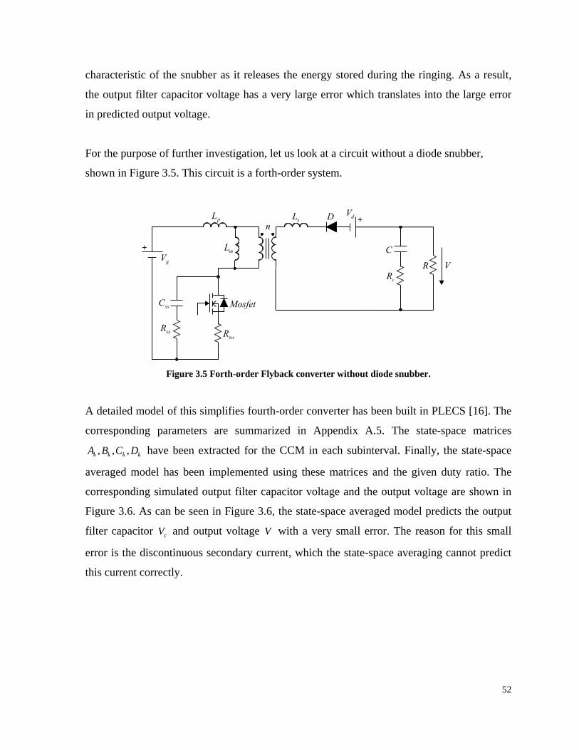
52
characteristic of the snubber as it releases the energy stored during the ringing. As a result,
the output filter capacitor voltage has a very large error which translates into the large error
in predicted output voltage.
For the purpose of further investigation, let us look at a circuit without a diode snubber,
shown in Figure 3.5. This circuit is a forth-order system.
+
+sL
mL
R
cR
ssRswR
C
ssC
gV
Mosfet
V
dVDn
pL
Figure 3.5 Forth-order Flyback converter without diode snubber.
A detailed model of this simplifies fourth-order converter has been built in PLECS [16]. The
corresponding parameters are summarized in Appendix A.5. The state-space matrices
, , ,k k k kA B C D have been extracted for the CCM in each subinterval. Finally, the state-space
averaged model has been implemented using these matrices and the given duty ratio. The
corresponding simulated output filter capacitor voltage and the output voltage are shown in
Figure 3.6. As can be seen in Figure 3.6, the state-space averaged model predicts the output
filter capacitor cV and output voltage V with a very small error. The reason for this small
error is the discontinuous secondary current, which the state-space averaging cannot predict
this current correctly.

53
-72.256
-72.252
-72.248
-72.244
-72.24
Vc (
Volt)
0.199991 0.199993 0.199995 0.199997 0.199999-72.28
-72.27
-72.26
-72.25
-72.24
-72.23
Time (s)
V (
Volt)
Detailed Model
Actual Average
State-Space Averaging
Figure 3.6 The simulated output filter capacitor and output voltage of the forth-order Flyback converter
without the diode snubber in CCM.
Let us now look at the averaged state-space equation (3.2) of the fort-order flyback converter.
The output filter capacitor voltage depends on only the secondary current. Since the state-
space averaging predicts the secondary current with an error, because of the discontinuity,
the output filter capacitor has the error but much less than the fifth-order model.
7 9
5 6 7
5 6
6 5
5
63.383 0 0 28042
0 8.116 10 1.316 10 0
2.561 10 1.548 10 1.548 10 23049
43000 2.561 10 2.561 10 3870
0 0
0 0
1.562 10 2.561 10
2.561 10
ss ss
cc
C C
pp
s
s
vv
v v
ii
ii
•
•
•
•
− − × × = × − × − × − × × −
+× ×
− × 43005
g
d
V
V
−
(3.2)
As it is shown in this Section, the state-space averaging has a problem when the diode
snubber is present. The way to fix this problem is to introduce the diode current as a variable

54
in the averaged state-space model. To achieve that, the circuit has to be separated into two
circuits as shown in Figure 3.7.
+
+
sL
mL
R
cR
ssR
dsR
swR
C
dsC
ssC
gV
Mosfet
V
dVDn
pL
1Circuit 2Circuit
Figure 3.7 Modified fifth-order Flyback converter circuit.
The Circuit 1 is a switched circuit, and on the other Circuit 2 is non switched and can be
removed from the state-space averaging. After such partitioning, it is easy to extract the state
matrices of the Circuit 1 in CCM or DCM for each subinterval using detailed model. Here,
the diode current must be defined as an output in the state-space model, which will be the
input of the Circuit 2. Then, the state-space equations of the Circuit 2 can either be extracted
from the detailed model or calculated analytically. After extracting state-space model for
these circuits, the overall system can be modelled in CCM as shown in Figure 3.8.
x Ax Bu
y Cx Eu
·
= +
= +
( ) ( )
( ) ( )1 1 2 2 1 1 2 2
1 1 2 2 1 1 2 2
x A d A d x B d B d u
y C d C d x E d E d u
·
= + + +
= + + +
State Variables
gV
dVdi
cv
v
ssCvdsCv
pi si
uu
State Variable
1Circuit 2Circuit Figure 3.8 Proposed state-space averaged model of the fifth-order Flyback converter using two sub-
circuits and sub-models.
If the proposed state-space averaged model is implemented, it will be seen that the predicted
output filter capacitor voltage cv and output voltage v is same as Figure 3.3, which is still

55
incorrect. The reason is that the diode current is a discontinuous variable, and so the state-
space averaging of the Circuit 1 does not predict the diode current correctly, which translates
into the corresponding error in the predicted output voltage.

56
Chapter 4 : Full-order Flyback Converter
4.1 State-Space Averaging in CCM
The full circuit considered in this Chapter is shown in Figure 4.1. This circuit corresponds to
the full-order Flyback converter with parasitics and two snubber circuits (one snubber in the
MOSFET and another snubber is on the secondary side with the diode). As mentioned
earlier, when the circuit gets complicated, it is no longer practical to derive the state
equations analytically. There are well defined algorithms [41] and software tools [14-16] that
automatically generate and dynamically update the state-space model for each new
topological state of the system being used. Regardless of the approach or tool used, it is
assumed that inside each subinterval ( )k the system state model may be expressed by the
system matrices , , ,k k k kA B C D .
+
+
sL
mL
R
cR
ssR
dsR
swR
C
dsC
ssC
gV
Mosfet
V
dVDn
pLpR
sR
Figure 4.1 Full-order Flyback converter circuit.
The detailed model has been implemented using PLECS [16]. The converter parameters are
summarized in Appendix A.6. The state matrices , , ,k k k kA B C D have been extracted for each
subinterval in CCM. Finally, the state-space model has been implemented using these
matrices and the given duty ratio. The simulated state variables are shown in Figure 4.2.

57
As can be seen in Figure 4.2, the state-space averaging predicts the switch snubber capacitor
voltage ( )ssCV , and the diode snubber capacitor voltage ( )
dsCV correctly as expected because
these are continuous state variables. However, the state-space averaging predicts the output
filter capacitor voltage ( )cV with a large error. Moreover, the transformers primary ( )pI and
secondary current( )sI , are also predicted with an error. First, the currents deviate from their
average values because of the oscillations seen during the topology changes and as a result
the assumption (2.163) is no longer valid as explained in Section 2.5. Second, both currents
are discontinuous variables although the converter operates in CCM. Regardless of the mode
of operation, CCM or DCM, these currents as individual state variables are discontinuous
and (2.161) is no longer accurate. In particular, the local average of the primary current in the
second interval ( )2d T is zero (see Figure 4.2), whereas the state-space averaging implies that
this value should be 2 pd i . Since 2d and pi are not zero, the result of the state-space
averaging is not zero. Similar scenario is applied to secondary current.
As a result, when it comes to state-space averaging of Flyback converters (if the transformer
model has leakage inductances, which means primary and secondary currents are state
variables), it needs special consideration in CCM as well as in DCM which will be explained
in Section4.2.

58
-80
-60
-40
-20
0
Vc
(Volt)
0
10
20
30
40
V Cs
s(V
olt)
-1
0
1
2
3
I p(V
olt)
-0.4
-0.2
0
0.2
0.4
I s(V
olt)
0.071399 0.071401 0.071403 0.071405 0.071407-100
0
100
200
Time (s)
VC
ds
(Volt)
Detailed Model
Actual Average
State-Space Averaging
Detailed ModelActual Average
Actual Average andState-Space Averaging
Actual Average andState-Space Averaging
Figure 4.2 Predicted state variables of full-order Flyback converter in CCM.

59
4.2 State-Space Averaging in DCM
The DCM operation of PWM converters differs from CCM operation by an additional time
interval in each switching cycle during which the inductor current or capacitor voltage is
clamped to zero. In Flyback converters, there is an exception in this case if there is a diode
snubber in the circuit. To demonstrate this point, a detailed model of the converter circuit
depicted in Figure 4.1 has been implemented using PLECS [16]. The corresponding
parameters are summarized in Appendix A.7. The state matrices , , ,k k k kA B C D have been
extracted for each subinterval in DCM. Finally, the state-space averaged model has been
implemented using these matrices and the given duty ratio. The resulting simulated state
variables are shown in Figure 4.3.

60
-100
-50
0
Vc
(Volt)
0
20
40
VC
ss
(Volt)
-0.2
0
0.2
I s(A
mp.)
0.099959 0.099961 0.099963 0.099965 0.099967-100
0
100
200
Time (s)
VC
ds
(Volt)
-0.5
0
0.5
1
1.5
I p(A
mp.)
Detailed Model
Actual Average
State-Space Averaging
Detailed ModelActual Average
Actual Average andState-Space Averaging
Actual Average andState-Space Averaging
1 sd T2 sd T 3 sd T
sT
see Fig 4.4
Figure 4.3 Simulated state variables of the full-order Flyback converter in DCM.

61
0.099963 0.099964 0.099965
-0.04
0
0.04
0.08
Time (s)
I s(A
mp
.)
3 sd T
Figure 4.4 Simulated transformer secondary current of the full-order Flyback converter in DCM.
During the first interval ( )1 sd T , when the MOSFET is on and the diode is off, the primary
side of the transformer stores the energy in the field. Right after the switch change its state,
the stored energy on primary side is transferred to the secondary side, and this energy is spent
during the second interval ( )2 sd T . In CCM, the switches go back to their original position
before this energy being spent. But in DCM this energy is spent before the switches change
their positions. That is where there is an exception. If there is no snubber circuit, after the
energy is spent, the secondary current will stay at zero until switches go back to their original
state. If there is a snubber circuit, after the energy is spent, the energy stored in the diode
snubber capacitor will flow in the other direction until it reaches zero or switches go back
their original state. This special case makes it difficult to identify 2d and 3d in the model
with the presence of parasitics, which will be explained is Section 4.3.1.
As can be seen in Figure 4.3, the state-space averaging predicts the switch snubber capacitor
voltage ( )ssCV , and the diode snubber capacitor voltage ( )
dsCV correctly as expected because
these are continuous state variables. However, the state-space averaging predicts the output
filter capacitor voltage ( )cV with a large error. The reason has already been explained in
Section 3.2. Also the transformer primary ( )pI and secondary current ( )sI are predicted with
an error. As explained in Section 4.1, these currents are discontinuous in either CCM or
DCM. As a result, the conventional state-space averaging method also does not produce the
correct results in DCM.

62
4.3 Parametric Average Value Modeling in CCM and DCM
In this Section, the parametric average-value modeling is extended to the full-order converter
operation in CCM and DCM, which to the best of our knowledge has not been done for the
transformer isolated topologies.
4.3.1 Model Implementation
A detailed model of the converter depicted in Figure 4.1 has been implemented using
PLECS. The system matrices ( ), , ,k k k kA B C D for each subinterval have been extracted
numerically using PLECS and Simulink. Since the detailed model has all the parasitics, the
extracted system matrices have all information required. The element of correction vector
( )M and ( )3d are obtained as parametric functions of the duty-cycle ( )1d , the diode current
( )di and the average value of the state variables ( )x . To obtain the values of ( )3 1,d d x and
( )1,M d x , the detailed model has been run in the operation region of interest (for example;
duty-cycle changes between 0.1 and 0.9, and the load ( )R changes from very low load to
very high load) whereas the state variables are averaged numerically over the prototyping
switching interval. In particular, the average-value of the state vector ( )x is computed in a
steady-state corresponding to given operation point. Specifically, in the steady-state from
equation(2.168) an intermediate vector p is computed using (2.169). Thereafter, the
elements of M are found using (2.170).
To obtain the functions ( )3 1,d d x and ( )1,M d x for the desired operation range, the detailed
simulation is run with different values of control variable ( )1d as well as the load resistance
( )R . The variables resulting from this procedure are 1 2 3 ,, , , , , , , ,ss dsd c C p s Cd d d R i v v i i v . Then, the
correction vector ( )M is computed using (2.169) and (2.170). These variables are stored for
future use in lookup tables. The real challenge here is to calculate the 2d or 3d at any given
operation point. As can be seen in Figure 4.3 and Figure 4.4, there is no easy way to read the
intervals from the state variables' waveforms because of the ringing waveforms caused by
snubbers. To achieve that, the diode current is used, as seen in Figure 4.5. As can be seen in

63
Figure 4.5 , the diode current is zero during the first and third subinterval. Since we know the
first interval, it becomes easy to calculate the third and then second subintervals.
0.105993 0.105995 0.105997 0.105999-0.16
-0.12
-0.08
-0.04
0
Time (s)
I d(A
mp.)
2 sd T ( )1 3 sd d T+
sT
Figure 4.5 The diode current waveform.
The final numerical function for 3d is plotted in Figure 4.6. The variable 3d has a flat surface
corresponding to CCM and varies linearly along the 1d . In DCM, the surface of 3d becomes
non-linear and increases.
As explained in Section 3.2, the filter capacitor voltage ( )cV has a large error even though it
is a continuous voltage. To fix this problem a model proposed in Section 3.2 (see Figure 3.8)
has been used here. If the secondary current is corrected, the diode current will be corrected
as well, and as a result the output capacitor voltage and the output voltage will be fixed
without a correction term. In the PAVM, the correction term 1m of filter capacitor voltage
( )cV can be set to 1.

64
0
1000
2000
3000
0.10.20.30.40.50.60.70.80.910
0.1
0.2
0.3
0.4
0.5
R (ohm)
d1
d3 CCM
DCM
Figure 4.6 Variable 3d as a function of the duty-cycle ( )1d and the load resistance ( )R .
The correction term ( )2m of the primary side snubber capacitor voltage ( )ssCV is plotted in
Figure 4.7 as a function of the duty-cycle ( )1d and the load resistance ( )R . The correction
term ( )3m of the primary current ( )pI is plotted in Figure 4.8 as a function of the duty-cycle
( )1d and the load resistance ( )R . The correction term of the primary current has no flat
surface because some correction is needed in CCM and DCM as explained in Section 4.1.
The correction term ( )4m of the secondary current ( )sI is plotted in Figure 4.9 as a function
of the duty-cycle ( )1d and the load resistance ( )R . Similar to correction term the secondary
current ( )3m , the current ( )sI is always discontinuous and needs correction in CCM and
DCM.

65
01000
20003000
0.10.20.30.40.50.60.70.80.96
0.98
1
1.02
1.04
R (ohm)
d1
m2
CCM and DCM
Figure 4.7 The correction term 2m as a function of duty-cycle ( )1d and the load resistance ( )R .
01000
20003000
0.10.20.30.40.50.60.70.80
2
4
6
8
10
12
14
R (ohm)
d1
m3
CCM and DCM
Figure 4.8 The correction term 3m as a function of the duty-cycle ( )1d and the load resistance ( )R .

66
0
1000
2000
3000
0.10.20.30.40.50.60.70.80.910
0.2
0.4
0.6
0.8
1
1.2
1.4
R (ohm)
d1
m4
CCM and DCM
Figure 4.9 The correction term 4m as a function of duty-cycle ( )1d and the load resistance ( )R .
The correction term ( )5m of the diode’s snubber capacitor voltage ( )dsCV is plotted in Figure
4.10. This correction term has a problem. Since the diode’s snubber capacitor voltage ( )dsCV
is a continuous state variable, the correction term must be equal to 1. In theory, the average
value of the diode snubber capacitor voltage is zero because it stores energy during one
interval and discharge this energy during another interval. As a result, the average value is
should be equal to zero. But when the value of p calculated using (2.170), it doesn’t give
exactly zero but gives very small numbers such as 132 10−⋅ due to the numerical precision of
calculations. Then this is used to calculate the correction term ( )5m . In theory, dsCv must be
equal to zero but in the detailed simulation again we get very small numbers because of the
ringing waveforms. Since the capacitor voltage is a continuous state variable, in the model
implementation the correction term ( )5m is set to 1.

67
0
10002000
3000
0.10.20.30.40.50.60.70.8-2
-1.5
-1
-0.5
0
0.5
1
1.5
2x10
-5
R (ohm)
d1
m5
CCM and DCM
Figure 4.10 The correction term 5m as a function of duty-cycle ( )1d and the load resistance ( )R .
Once the functions ( )3 1,d d x and ( )1,M d x are available and stored, the parametric average-
value model can be implemented as explained in section 2.5.2.
4.4 Case Studies
The flyback converter shown in Figure 4.1 is used for case studies. The detailed model is
implemented in PLECS [16]. The converters parameters are summarized in the AppendixA.6
and A.7 in CCM and DCM, respectively, correspond to the hardware prototype that has been
built, Appendix B. The proposed model, Figure 2.16, has been implemented and compared to
the hardware prototype, the detailed model and conventional state-space averaging model in
both time and frequency domains.
4.4.1 Time Domain
To demonstrate the parametric average-value model in CCM, the following study has been
implemented in the detailed model, the hardware prototype, the conventional stat-space
averaged model and the proposed PAVM. The system is assumed to initially operate in a
steady state defined by 1 0.381d = and 717.05R= Ω . The resulting measured and simulated
output voltage, the primary current and the secondary current shown in Figure 4.11.
As can be seen in Figure 4.11, the developed PAVM predicts the average-value of the
waveforms well in CCM as compared to conventional state-space averaging which does not.

68
There is a difference between measured output voltage and detailed model’s output voltage.
The reason is that the detailed model doesn’t have all the parameters the hardware model has
such as stray capacitances.
-71.7
-71.6
-71.5
-71.4
V (
Vo
lt)
0
1
2
I p(A
mp
.)
0.009992 0.009993 0.009994 0.009995 0.009996-0.4
-0.2
0
0.2
0.4
Time (s)
I s(A
mp
.)
Detailed Model
Hardware Prototype
Actual Average
PAVM
Detailed Model
State-Space Averaging
Actual Average
PAVM
Detailed Model
Actual Averageand PAVM
Actual Averageand PAVM
Actual Averageand PAVM
Figure 4.11 Measured and simulated output voltage, primary and secondary current in CCM at constant
duty-cycle.
The accuracy of the PAVM in predicting the large-signal behaviour in time-domain has also
been verified by studying the effect of sudden change in load. In the following study, the
output of the flyback converter was regulated using the same PI controller designed to
regulate the output voltage at 72V− . In the study being considered, the converter initially
operate in DCM with a 2000Ω load. At 0.01t s= , a parallel load of 500Ω is added which
changes the mode to CCM. The resulting time-domain transients are shown in Figure 4.12.
After load changes the control action brings the output voltage to the desired72V− . Through

69
all transients, the large signal behaviour of the detailed model is accurately predicted by
developed PAVM.
-72
-71.9
-71.8
-71.7V
(V
olt)
-2
-1
0
1
2
3
4
I p(A
mp.)
0.0098 0.0102 0.0106 0.011 0.0114-1
-0.5
0
0.5
Time (s)
I s(A
mp.)
Detailed Model
PAVM
Detailed Model
PAVM
Detailed Model PAVM
Figure 4.12 Simulated output voltage, primary and secondary current during the transient from DCM to
CCM due to the step change in load.
4.4.2 Frequency Domain
The control-to-output transfer function of the full-order converter predicted by the detailed
and the developed PAVM models have been extracted again for the full load operating point
defined by 717.05R= Ω and 1 0.381d = . The magnitude and phase of the corresponding
function are plotted in Figure 4.13. As can be seen in this figure, the developed PAVM
predicts the small-signal characteristic with good agreement with the detailed switching
model.

70
-40
-20
0
20
40
60
Am
plit
ude (
dB
)
102
103
104
105
0
20
40
60
80
100
120
140
160
Phase (
°)
Frequency (Hz)
PAVM
DetailedModel
DetailedModel
PAVM
Figure 4.13 Control-to-output transfer function of the full-order Flyback converter evaluated at
717.05R= Ω and 1 0.381d = .
4.4.3 Efficiency Results
One of the most common use of averaged models is system level modeling, wherein the
models only appear as a black box in the system level modeling with input and output ports.
It is therefore very important that the developed model accurately predicts the terminal
characteristics of the converter module. Among such terminal characteristics the total
converter efficiency is of significant importance. The comparisons of efficiencies predicted
by various averaged models are shown in Table 4.1 assuming the converter operates at full
load in CCM, ( )1717.05 , 0.381R d= Ω = .
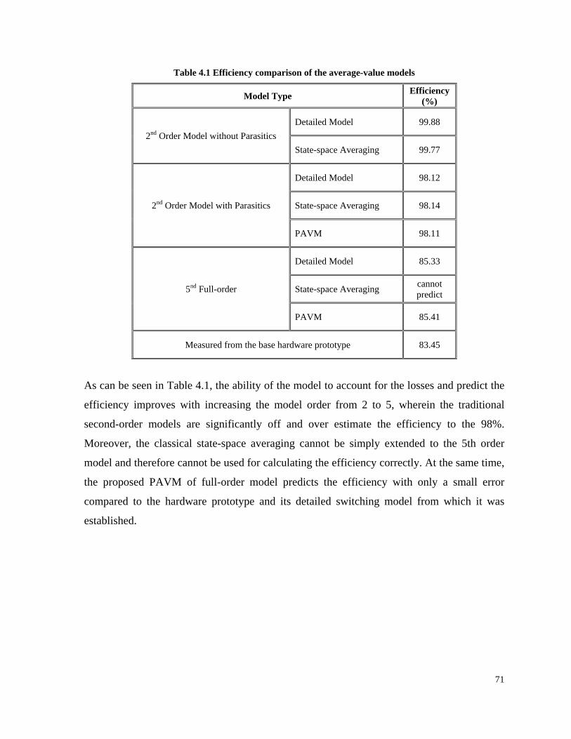
71
Table 4.1 Efficiency comparison of the average-value models
Model Type Efficiency (%)
2nd Order Model without Parasitics
Detailed Model 99.88
State-space Averaging 99.77
2nd Order Model with Parasitics
Detailed Model 98.12
State-space Averaging 98.14
PAVM 98.11
5nd Full-order
Detailed Model 85.33
State-space Averaging cannot predict
PAVM 85.41
Measured from the base hardware prototype 83.45
As can be seen in Table 4.1, the ability of the model to account for the losses and predict the
efficiency improves with increasing the model order from 2 to 5, wherein the traditional
second-order models are significantly off and over estimate the efficiency to the 98%.
Moreover, the classical state-space averaging cannot be simply extended to the 5th order
model and therefore cannot be used for calculating the efficiency correctly. At the same time,
the proposed PAVM of full-order model predicts the efficiency with only a small error
compared to the hardware prototype and its detailed switching model from which it was
established.

72
Chapter 5 : Conclusion
In this Thesis, the recently established parametric average-value modeling methodology has
been extended to the transformer-isolated Flyback converter topology which includes
parasitics and snubbers. It is shown that the developed model captures includes the effect
parasitics and losses, and is therefore capable of accurately predicting the terminal
characteristics of the converter such as efficiency with the accuracy that has not been
attainable by any previously established average-value models. The developed method
overcomes the complexity and challenges common to many previously developed models
when the parasitics of the circuit elements and snubbers are considered. The numerically
constructed model can function in both CCM and DCM. It has been shown that obtaining an
accurate full order average-value model requires extracting the duty-ratio constraint and the
correction term. The functions of the duty-ratio constraint and correction terms were obtained
numerically by running the detailed simulation at desired operation range. Once the model
established, the resulting model is continuous and valid for large-signal time-domain
transient studies as well as for linearization and subsequent small-signal characterization of
the overall system over a wide range.
It has also been shown that direct application of conventional state-space averaging method
is no longer accurate for flyback converters in CCM when the transformer leakage
inductances are taken into account. A detailed analysis of flyback converters working in
CCM has been done to present the problems in CCM. Regardless of the converter operating
mode (CCM or DCM) the primary and secondary currents are discontinuous. As a result, the
conventional assumptions used for DC-DC converters are no longer acceptable for flyback
converters.
5.1 Future Work
As a next step, the parametric average-value modeling can be extended to other DC-DC
topologies such as forward converters (H Bridge) and Push Pull converters for high voltage
applications to have a full set of models for DC-DC converters. Another potential topic for

73
future research could be to investigate the converters with source ripple and input filters
using PAVM. Since it is very easy to include parasitics in PAVM, one could also include in
the model stray capacitances and core losses in the magnetic components.
There are other kinds of snubber circuits in the practical applications such as RCD
(resistance, capacitance and diode) and active snubbers. They also could be included in
PAVM.

74
Bibliography
[1] K.-H. Liu and F. Lee, “Topological constraints on basic pwm converters,” in Power
Electronics Specialists Conference, 1988. PESC ’88 Record., 19th Annual IEEE.
IEEE, april 1988, pp. 164 –172 vol.1.
[2] D. Maksimovic, “Synthesis of pwm and quasi-resonant dc-to-dc power converters,”
Ph.D. dissertation, 1989.
[3] D. Maksimovic and S. Cuk, “A unified analysis of pwm converters in discontinuous
modes,” Power Electronics, IEEE Transactions on, vol. 6, no. 3, pp. 476 –490, jul
1991.
[4] J. Sun, D. Mitchell, M. Greuel, P. Krein, and R. Bass, “Averaged modeling of pwm
converters operating in discontinuous conduction mode,” Power Electronics, IEEE
Transactions on, vol. 16, no. 4, pp. 482 –492, Jul. 2001.
[5] D. Maksimovic and S. Cuk, “General properties and synthesis of pwm dc-to-dc
converters,” in Power Electronics Specialists Conference, 1989. PESC ’89 Record.,
20th Annual IEEE. IEEE, jun 1989, pp. 515 –525 vol.2.
[6] P. Krein and R. Bass, “Geometric formulation, classification and methods for power
electronic systems,” in Power Electronics Specialists Conference, 1990. PESC ’90
Record., 21st Annual IEEE. IEEE, jun 1990, pp. 499 –505.
[7] R. Tymerski and V. Vorperian, “Generation, classification and analysis of switched-
mode dc-to-dc converters by the use of converter cells,” in Telecommunications
Energy Conference, 1986. INTELEC ’86. International. IEEE, oct. 1986, pp. 181 –
195.
[8] J. Sun and H. Grotstollen, “Averaged modelling of switching power converters:
reformulation and theoretical basis,” pp. 1165 –1172 vol.2, Jul. 1992.
[9] A. Pressman, K. Billings, and T. Morey, Switching power supply design. McGraw-
Hill Professional, 2009.
[10] R. Erickson and D. Maksimovic, Fundamentals of power electronics. Springer
Netherlands, 2001.
[11] S. Ang and A. Oliva, Power-switching converters. CRC, 2005, vol. 123.

75
[12] M. Kazimierczuk and S. Nguyen, “Small-signal analysis of open-loop pwm flyback
dc-dc converter for ccm,” in Aerospace and Electronics Conference, 1995. NAECON
1995., Proceedings of the IEEE 1995 National, vol. 1. IEEE, may 1995, pp. 69 –76
vol.1.
[13] H. Kewei, L. Jie, F. Ningjun, L. Yuebin, H. Xiaolin, and W. Luo, “Modeling analysis
and simulation of high-voltage flyback dc-dc converter,” in Industrial Electronics,
2009. ISIE 2009. IEEE International Symposium on. IEEE, july 2009, pp. 813 –818.
[14] SimPowerSystems User’s Guide Version 5, Hydro-Quebec, The Mathworks Inc.,
2010. [Online]. Available: www.mathworks.com
[15] Automated State Model Generator (ASMG), PC Krause and Associates Inc., 2002.
[Online]. Available: www.pcka.com
[16] Piece-wise Linear Electrical Circuit Simulation for Simulink (PLECS), Plexim
GmbH, 2009. [Online]. Available: www.plexim.com
[17] D. Czarkowski and M. Kazimierczuk, “Linear circuit models of pwm flyback and
buck/boost converters,” Circuits and Systems I: Fundamental Theory and
Applications, IEEE Transactions on, vol. 39, no. 8, pp. 688 –693, aug 1992.
[18] R. Middlebrook and S. Cúk, “A general unified approach to modelling switching-
converter power stages,” International Journal of Electronics, vol. 42, no. 6, pp. 521–
550, 1977.
[19] P. Chetty, “Current injected equivalent circuit approach to modeling switching dc-dc
converters,” Aerospace and Electronic Systems, IEEE Transactions on, vol. AES-17,
no. 6, pp. 802 –808, nov. 1981.
[20] S. Cúk and R. Middlebrook, “A general unified approach to modeling switching dc-
to-dc converters in discontinuous conduction mode,” in in Proc. IEEE PESC’77,
1977, pp. 36–57.
[21] V. Vorperian, “Simplified analysis of pwm converters using the model of the pwm
switch parts i and 11,” IEEE Trans. on Aerospace and Electronic Systems, vol. 26,
no. 3, pp. 490–505, 1990.
[22] J. Jatskevich, S. Pekarek, and A. Davoudi, “Parametric average-value model of
synchronous machine-rectifier systems,” Energy Conversion, IEEE Transactions on,
vol. 21, no. 1, pp. 9 – 18, 2006.

76
[23] ——, “A fast procedure for constructing an accurate dynamic average-value model of
synchronous machine-rectifier systems,” in Power Engineering Society General
Meeting, 2006. IEEE, 0-0 2006, p. 1 pp.
[24] A. Davoudi, J. Jatskevich, and T. De Rybel, “Numerical state-space average-value
modeling of pwm dc-dc converters operating in dcm and ccm,” Power Electronics,
IEEE Transactions on, vol. 21, no. 4, pp. 1003 – 1012, 2006.
[25] A. Davoudi and J. Jatskevich, “Realization of parasitics in state-space average-value
modeling of pwm dc-dc converters,” Power Electronics, IEEE Transactions on,
vol. 21, no. 4, pp. 1142 – 1147, 2006.
[26] A. Davoudi, J. Jatskevich, and P. Chapman, “Computer-aided average-value
modeling of fourth-order pwm dc-dc converters,” pp. 793 –796, May 2007.
[27] ——, “Computer-aided dynamic characterization of fourth-order pwm dc-dc
converters,” Circuits and Systems II: Express Briefs, IEEE Transactions on, vol. 55,
no. 10, pp. 1021 –1025, 2008.
[28] J. Sun, “Unified averaged switch models for stability analysis of large distributed
power systems,” in Applied Power Electronics Conference and Exposition, 2000.
APEC 2000. Fifteenth Annual IEEE, vol. 1, 2000, pp. 249 –255 vol.1.
[29] G. Wester and R. Middlebrook, “Low-frequency characterization of switched dc-dc
converters,” Aerospace and Electronic Systems, IEEE Transactions on, vol. AES-9,
no. 3, pp. 376 –385, may 1973.
[30] Matlab/Simulink 7 User’s Guide, The Mathworks Inc., 2010. [Online]. Available:
www.mathworks.com
[31] S. Howimanporn and C. Bunlaksananusorn, “Performance comparison of continuous
conduction mode (ccm) and discontinuous conduction mode (dcm) flyback
converters,” in Power Electronics and Drive Systems, 2003. PEDS 2003. The Fifth
International Conference on, vol. 2, nov. 2003, pp. 1434 – 1438 Vol.2.
[32] D. Hart, Introduction to power electronics. Prentice Hall PTR Upper Saddle River,
NJ, USA, 1996.
[33] J. Mahdavi, A. Emaadi, M. Bellar, and M. Ehsani, “Analysis of power electronic
converters using the generalized state-space averaging approach,” Circuits and

77
Systems I: Fundamental Theory and Applications, IEEE Transactions on, vol. 44,
no. 8, pp. 767 –770, Aug. 1997.
[34] R. Brockett and J. Wood, “Electrical networks containing controlled switches,” In its
Appl. of System Theory to Power Process. Probl. p 57-79 (SEE, vol. 75, 1974.
[35] C. Meyer, Matrix analysis and applied linear algebra and solutions manual. Society
for Industrial and Applied Mathematics, 2000.
[36] M. Spiegel, Schaum’s outline of theory and problems of advanced mathematics for
engineers and scientists. Schaum’s Outline Series, 1971.
[37] N. Mohan, T. Undeland, and W. Robbins, Power electronics. Wiley New York, 1995.
[38] J. Kassakian, M. Schlecht, and G. Verghese, Principles of power electronics.
Addison-Wesley Reading, MA, 1991.
[39] R. Ridley, “Flyback converter snubber design,” Switching Power Magazine, 2005.
[Online]. Available: http://www.ridleyengineering.com
[40] A. Elasser and D. Torrey, “Soft switching active snubbers for dc/dc converters,”
Power Electronics, IEEE Transactions on, vol. 11, no. 5, pp. 710 –722, Sep. 1996.
[41] L. O. Chua and P. Y. Lin, Computer-Aided Analysis of Electronic Circuits:
Algorithms and Computational Techniques. Prentice Hall Professional Technical
Reference, 1975.

78
Appendices
Appendix A. The Converters Circuit Parameters
A.1 Second-order Flyback Converter Parameters without Parasitics in CCM
1
20.009
:3.8 ,55 , , Re 2705
250
0.381
: 0635
27
1/ 6
:1 ,400 , cov , 1 04
2
g
s
m
v V
Mosfet A V N chanel International ctifier IRLL
f kHz
d
Transformer ICEComponents ICA
L H
n
Diode A V ultra fast re ery diode Central Semiconductor CorpCMR U
C
µ
=
−==
−=
=− −
= 2 ,100 , min , 100 22
717.05
F V alu umelectrolyticcapacitor Sanyo MV AX
R
µ= Ω
A.2 Second-order Flyback Converter Parameters without Parasitics in DCM
1 220.009 , 250 , 0.381, 0.4409
27 , 1/ 6, 22 , 2500g s
m
v V f kHz d d
L H n C F Rµ µ= = = =
= = = = Ω
A.3 Second-order Flyback Converter Parameters with Parasitics in CCM
1
20.009
:3.8 ,55 , , Re 2705
0.04
250
0.381
: 0635
27
1/ 6
:1 ,400 , cov ,
g
sw
s
m
v V
Mosfet A V N chanel International ctifier IRLL
R
f kHz
d
Transformer ICEComponents ICA
L H
n
Diode A V ultra fast re ery diode Central Semiconductor CorpCM
µ
=
−= Ω
==
−=
=− 1 04
1.25
22 ,100 , min , 100 22
0.09
717.05
d
c
R U
V V
C F V alu umelectrolyticcapacitor Sanyo MV AX
R
R
µ
−=
== Ω
= Ω

79
A.4 Second-order Flyback Converter Parameters with Parasitics in DCM
1 220.009 , 250 , 0.381, 0.4409
27 , 1/ 6, 22 , 2500
0.04 , 1.25 , 0.09
g s
m
sw d c
v V f kHz d d
L H n C F R
R V V R
µ µ= = = =
= = = = Ω= Ω = = Ω
A.5 Fifth-order Flyback Converter Parameters in CCM
1
20.009
:3.8 ,55 , , Re 2705
0.04 , 250
0.381
470 , 10
: 0635
27 , 0.2 , 0.8
1/ 6
:1 ,400 , co
g
sw s
ss ss
m p s
v V
Mosfet A V N chanel International ctifier IRLL
R f kHz
d
C pF R
Transformer ICEComponents ICA
L H L H L H
n
Diode A V ultra fast re
µ µ µ
=
−= Ω =
== = Ω
−= = =
=− v , 1 04
1.25
100 , 200
22 ,100 , min , 100 22 , 0.09
717.05
d
ds ds
c
ery diode Central Semiconductor CorpCMR U
V V
C pF R
C F V alu umelectrolyticcapacitor Sanyo MV AX R
R
µ
−== = Ω
= = Ω= Ω
A.6 Full-order Flyback Converter Parameters in CCM
1
20.009
:3.8 ,55 , , Re 2705
0.04 , 250
0.381
470 , 10
: 0635
27 , 0.2 , 0.8
210 , 1.35
1/ 6
:1 ,40
g
sw s
ss ss
m p s
p s
v V
Mosfet A V N chanel International ctifier IRLL
R f kHz
d
C pF R
Transformer ICEComponents ICA
L H L H L H
R m R
n
Diode A
µ µ µ
=
−= Ω =
== = Ω
−= = =
= Ω = Ω
=0 , cov , 1 04
1.25
100 , 200
22 ,100 , min , 100 22 , 0.09
717.05
d
ds ds
c
V ultra fast re ery diode Central Semiconductor CorpCMR U
V V
C pF R
C F V alu umelectrolyticcapacitor Sanyo MV AX R
R
µ
− −== = Ω
= = Ω= Ω

80
A.7 Full-order Flyback Converter Parameters in DCM
1
20.009
:3.8 ,55 , , Re 2705
0.04 , 250
0.381
470 , 10
: 0635
27 , 0.2 , 0.8
210 , 1.35
1/ 6
:1 ,40
g
sw s
ss ss
m p s
p s
v V
Mosfet A V N chanel International ctifier IRLL
R f kHz
d
C pF R
Transformer ICEComponents ICA
L H L H L H
R m R
n
Diode A
µ µ µ
=
−= Ω =
== = Ω
−= = =
= Ω = Ω
=0 , cov , 1 04
1.25
100 , 200
22 ,100 , min , 100 22 , 0.09
2500
d
ds ds
c
V ultra fast re ery diode Central Semiconductor CorpCMR U
V V
C pF R
C F V alu umelectrolyticcapacitor Sanyo MV AX R
R
µ
− −== = Ω
= = Ω= Ω

81
Appendix B. Flyback Converter Circuit Diagram


![Catalogue FLYBACK Equivalent - [PDF Document] FLYBACK Equivalent FlyBack Equivalent flyback reemplazo conversor Flyback tv fly-back Flyback Tester Flyback Converter conversor Flyback](https://img.pdfslide.us/doc/110x75/5a832a447f8b9a9d308e9416/catalogue-flyback-equivalent-pdf-document-flyback-equivalent-flyback-equivalent.jpg)