Embed Size (px)
Citation preview
INV ITEDP A P E R
Three Ages of FPGAs: ARetrospective on the First ThirtyYears of FPGA TechnologyThis paper reflects on how Moore’s Law has driven the design of FPGAs through
three epochs: the age of invention, the age of expansion, and the age of accumulation.
By Stephen M. (Steve) Trimberger, Fellow IEEE
ABSTRACT | Since their introduction, field programmable gate
arrays (FPGAs) have grown in capacity by more than a factor of
10 000 and in performance by a factor of 100. Cost and energy
per operation have both decreased by more than a factor of
1000. These advances have been fueled by process technology
scaling, but the FPGA story is much more complex than simple
technology scaling. Quantitative effects of Moore’s Law have
driven qualitative changes in FPGA architecture, applications
and tools. As a consequence, FPGAs have passed through sev-
eral distinct phases of development. These phases, termed
‘‘Ages’’ in this paper, are The Age of Invention, The Age of
Expansion and The Age of Accumulation. This paper summa-
rizes each and discusses their driving pressures and funda-
mental characteristics. The paper concludes with a vision of the
upcoming Age of FPGAs.
KEYWORDS | Application-specific integrated circuit (ASIC);
commercialization; economies of scale; field-programmable
gate array (FPGA); industrial economics; Moore’s Law; pro-
grammable logic
I . INTRODUCTION
Xilinx introduced the first field programmable gate arrays
(FPGAs) in 1984, though they were not called FPGAs until
Actel popularized the term around 1988. Over the ensuing
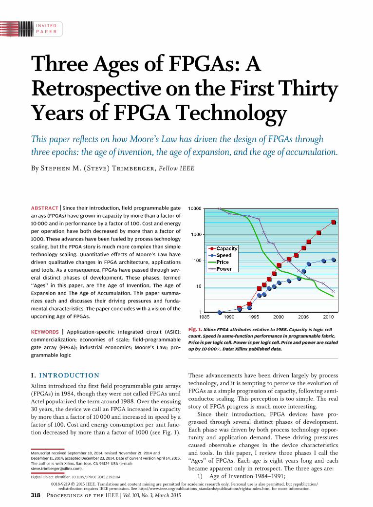
30 years, the device we call an FPGA increased in capacityby more than a factor of 10 000 and increased in speed by a
factor of 100. Cost and energy consumption per unit func-
tion decreased by more than a factor of 1000 (see Fig. 1).
These advancements have been driven largely by process
technology, and it is tempting to perceive the evolution of
FPGAs as a simple progression of capacity, following semi-
conductor scaling. This perception is too simple. The real
story of FPGA progress is much more interesting.
Since their introduction, FPGA devices have pro-
gressed through several distinct phases of development.
Each phase was driven by both process technology oppor-tunity and application demand. These driving pressures
caused observable changes in the device characteristics
and tools. In this paper, I review three phases I call the
‘‘Ages’’ of FPGAs. Each age is eight years long and each
became apparent only in retrospect. The three ages are:
1) Age of Invention 1984–1991;
Manuscript received September 18, 2014; revised November 21, 2014 and
December 11, 2014; accepted December 23, 2014. Date of current version April 14, 2015.
The author is with Xilinx, San Jose, CA 95124 USA (e-mail:
Digital Object Identifier: 10.1109/JPROC.2015.2392104
Fig. 1. Xilinx FPGA attributes relative to 1988. Capacity is logic cell
count. Speed is same-function performance in programmable fabric.
Price is per logic cell. Power is per logic cell. Price and power are scaled
up by 10 000�. Data: Xilinx published data.
0018-9219 � 2015 IEEE. Translations and content mining are permitted for academic research only. Personal use is also permitted, but republication/redistribution requires IEEE permission. See http://www.ieee.org/publications_standards/publications/rights/index.html for more information.
318 Proceedings of the IEEE | Vol. 103, No. 3, March 2015
2) Age of Expansion 1992–1999;3) Age of Accumulation 2000–2007.
II . PREAMBLE: WHAT WAS THEBIG DEAL ABOUT FPGAs?
A. FPGA Versus ASICIn the 1980s, Application-Specific Integrated Circuit
(ASIC) companies brought an amazing product to the
electronics market: the built-to-order custom integrated
circuit. By the mid-1980s, dozens of companies were sell-
ing ASICs, and in the fierce competition, the winning at-
tributes were low cost, high capacity and high speed. When
FPGAs appeared, they compared poorly on all of these
measures, yet they thrived. Why?The ASIC functionality was determined by custom mask
tooling. ASIC customers paid for those masks with an up-
front non-recurring engineering (NRE) charge. Because
they had no custom tooling, FPGAs reduced the up-front
cost and risk of building custom digital logic. By making
one custom silicon device that could be used by hundreds or
thousands of customers, the FPGA vendor effectively
amortized the NRE costs over all customers, resulting inno NRE charge for any one customer, while increasing the
per-unit chip cost for all.
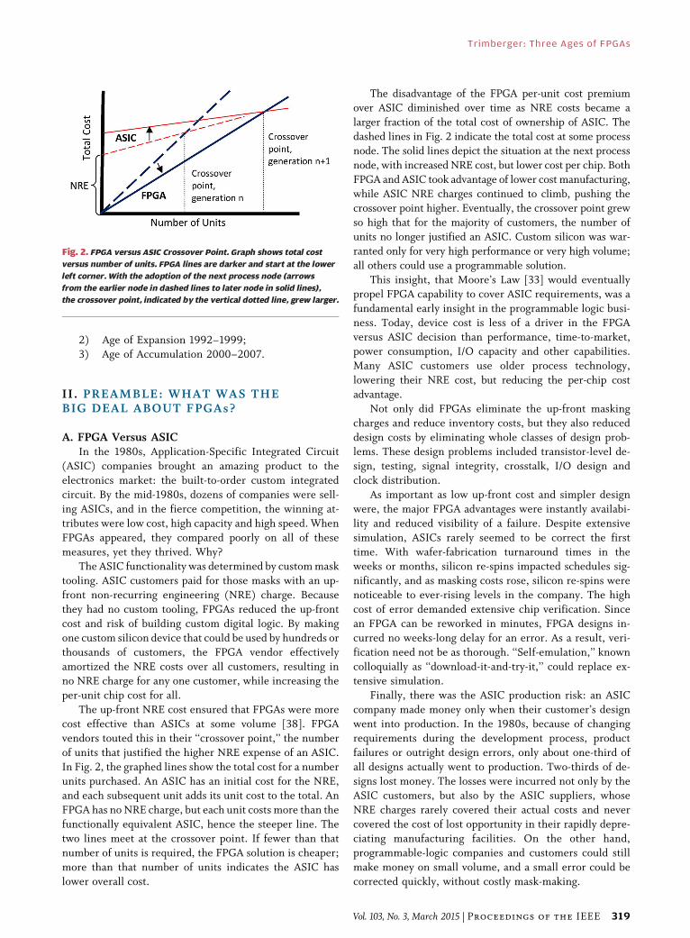
The up-front NRE cost ensured that FPGAs were more
cost effective than ASICs at some volume [38]. FPGA
vendors touted this in their ‘‘crossover point,’’ the number
of units that justified the higher NRE expense of an ASIC.
In Fig. 2, the graphed lines show the total cost for a number
units purchased. An ASIC has an initial cost for the NRE,and each subsequent unit adds its unit cost to the total. An
FPGA has no NRE charge, but each unit costs more than the
functionally equivalent ASIC, hence the steeper line. The
two lines meet at the crossover point. If fewer than that
number of units is required, the FPGA solution is cheaper;
more than that number of units indicates the ASIC has
lower overall cost.
The disadvantage of the FPGA per-unit cost premiumover ASIC diminished over time as NRE costs became a
larger fraction of the total cost of ownership of ASIC. The
dashed lines in Fig. 2 indicate the total cost at some process
node. The solid lines depict the situation at the next process
node, with increased NRE cost, but lower cost per chip. Both
FPGA and ASIC took advantage of lower cost manufacturing,
while ASIC NRE charges continued to climb, pushing the
crossover point higher. Eventually, the crossover point grewso high that for the majority of customers, the number of
units no longer justified an ASIC. Custom silicon was war-
ranted only for very high performance or very high volume;
all others could use a programmable solution.
This insight, that Moore’s Law [33] would eventually
propel FPGA capability to cover ASIC requirements, was a
fundamental early insight in the programmable logic busi-
ness. Today, device cost is less of a driver in the FPGAversus ASIC decision than performance, time-to-market,
power consumption, I/O capacity and other capabilities.
Many ASIC customers use older process technology,
lowering their NRE cost, but reducing the per-chip cost
advantage.
Not only did FPGAs eliminate the up-front masking
charges and reduce inventory costs, but they also reduced
design costs by eliminating whole classes of design prob-lems. These design problems included transistor-level de-
sign, testing, signal integrity, crosstalk, I/O design and
clock distribution.
As important as low up-front cost and simpler design
were, the major FPGA advantages were instantly availabi-
lity and reduced visibility of a failure. Despite extensive
simulation, ASICs rarely seemed to be correct the first
time. With wafer-fabrication turnaround times in theweeks or months, silicon re-spins impacted schedules sig-
nificantly, and as masking costs rose, silicon re-spins were
noticeable to ever-rising levels in the company. The high
cost of error demanded extensive chip verification. Since
an FPGA can be reworked in minutes, FPGA designs in-
curred no weeks-long delay for an error. As a result, veri-
fication need not be as thorough. ‘‘Self-emulation,’’ known
colloquially as ‘‘download-it-and-try-it,’’ could replace ex-tensive simulation.
Finally, there was the ASIC production risk: an ASIC
company made money only when their customer’s design
went into production. In the 1980s, because of changing
requirements during the development process, product
failures or outright design errors, only about one-third of
all designs actually went to production. Two-thirds of de-
signs lost money. The losses were incurred not only by theASIC customers, but also by the ASIC suppliers, whose
NRE charges rarely covered their actual costs and never
covered the cost of lost opportunity in their rapidly depre-
ciating manufacturing facilities. On the other hand,
programmable-logic companies and customers could still
make money on small volume, and a small error could be
corrected quickly, without costly mask-making.
Fig. 2. FPGA versus ASIC Crossover Point. Graph shows total cost
versus number of units. FPGA lines are darker and start at the lower
left corner. With the adoption of the next process node (arrows
from the earlier node in dashed lines to later node in solid lines),
the crossover point, indicated by the vertical dotted line, grew larger.
Trimberger: Three Ages of FPGAs
Vol. 103, No. 3, March 2015 | Proceedings of the IEEE 319
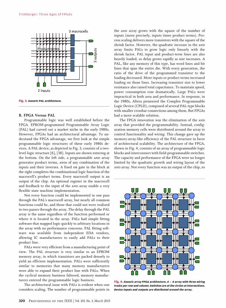
B. FPGA Versus PALProgrammable logic was well established before the
FPGA. EPROM-programmed Programmable Array Logic
(PAL) had carved out a market niche in the early 1980s.
However, FPGAs had an architectural advantage. To un-
derstand the FPGA advantage, we first look at the simple
programmable logic structures of these early 1980s de-vices. A PAL device, as depicted in Fig. 3, consists of a two-
level logic structure [6], [38]. Inputs are shown entering at
the bottom. On the left side, a programmable and array
generates product terms, ands of any combination of the
inputs and their inverses. A fixed or gate in the block at
the right completes the combinational logic function of the
macrocell’s product terms. Every macrocell output is an
output of the chip. An optional register in the macrocelland feedback to the input of the and array enable a very
flexible state machine implementation.
Not every function could be implemented in one pass
through the PAL’s macrocell array, but nearly all common
functions could be, and those that could not were realized
in two passes through the array. The delay through the PAL
array is the same regardless of the function performed or
where it is located in the array. PALs had simple fittingsoftware that mapped logic quickly to arbitrary locations in
the array with no performance concerns. PAL fitting soft-
ware was available from independent EDA vendors,
allowing IC manufacturers to easily add PALs to their
product line.
PALs were very efficient from a manufacturing point of
view. The PAL structure is very similar to an EPROM
memory array, in which transistors are packed densely toyield an efficient implementation. PALs were sufficiently
similar to memories that many memory manufacturers
were able to expand their product line with PALs. When
the cyclical memory business faltered, memory manufac-
turers entered the programmable logic business.
The architectural issue with PALs is evident when one
considers scaling. The number of programmable points in
the and array grows with the square of the number ofinputs (more precisely, inputs times product terms). Pro-
cess scaling delivers more transistors with the square of the
shrink factor. However, the quadratic increase in the and
array limits PALs to grow logic only linearly with the
shrink factor. PAL input and product-term lines are also
heavily loaded, so delay grows rapidly as size increases. A
PAL, like any memory of this type, has word lines and bit
lines that span the entire die. With every generation, theratio of the drive of the programmed transistor to the
loading decreased. More inputs or product terms increased
loading on those lines. Increasing transistor size to lower
resistance also raised total capacitance. To maintain speed,
power consumption rose dramatically. Large PALs were
impractical in both area and performance. In response, in
the 1980s, Altera pioneered the Complex Programmable
Logic Device (CPLD), composed of several PAL-type blockswith smaller crossbar connections among them. But FPGAs
had a more scalable solution.
The FPGA innovation was the elimination of the and
array that provided the programmability. Instead, config-
uration memory cells were distributed around the array to
control functionality and wiring. This change gave up the
memory-array-like efficiency of the PAL structure in favor
of architectural scalability. The architecture of the FPGA,shown in Fig. 4, consists of an array of programmable logic
blocks and interconnect with field-programmable switches.
The capacity and performance of the FPGA were no longer
limited by the quadratic growth and wiring layout of the
and array. Not every function was an output of the chip, so
Fig. 3. Generic PAL architecture.
Fig. 4. Generic array FPGA architecture. 4� 4 array with three wiring
tracks per row and column. Switches are at the circles at intersections.
Device inputs and outputs are distributed around the array.
Trimberger: Three Ages of FPGAs
320 Proceedings of the IEEE | Vol. 103, No. 3, March 2015
capacity could grow with Moore’s Law. The consequenceswere great.
• FPGA architecture could look nothing like a mem-
ory. Design and manufacturing were very different
than memory.
• The logic blocks were smaller. There was no gua-
rantee that a single function would fit into one.
Therefore, it was difficult to determine ahead of
time how much logic would fit into the FPGA.• The performance of the FPGA depended on where
the logic was placed in the FPGA. FPGAs required
placement and routing, so the performance of the
finished design was not easy to predict in advance.
• Complex EDA software was required to fit a design
into an FPGA.
With the elimination of the and-array, FPGA architects
had the freedom to build any logic block and any inter-connect pattern. FPGA architects could define whole new
logic implementation models, not based on transistors or
gates, but on custom function units. Delay models need
not be based on metal wires, but on nodes and switches.
This architectural freedom ushered in the first Age of
FPGAs, the Age of Invention.
III . AGE OF INVENTION 1984–1991
The first FPGA, the Xilinx XC2064, contained only 64 logic
blocks, each of which held two three-input Look-Up Tables
(LUTs) and one register [8]. By today’s counting, this would
be about 64 logic cells, less than 1000 gates. Despite its
small capacity, it was a very large dieVlarger than the
commercial microprocessors of the day. The 2.5-micron
process technology used for the XC2064 was barely able toyield it. In those early years, cost containment was critical
to the success of FPGAs.
‘‘Cost containment was critical to the success of FPGAs.’’
A modern reader will accept that statement as some kind of
simplistic statement of the obvious, but this interpretation
seriously underemphasizes the issue. Die size and cost per
function were crushingly vital. The XC2064, with only
64 user-accessible flip-flops, cost hundreds of dollars becauseit was such a large die. Since yield (and hence, cost) is super-
linear for large die, a 5% increase in die size could have
doubled the cost or, worse, yield could have dropped to zero
leaving the startup company with no product whatsoever.
Cost containment was not a question of mere optimization; it
was a question of whether or not the product would exist. It
was a question of corporate life or death. In those early years,
cost containment was critical to the success of FPGAs.As a result of cost pressure, FPGA architects used their
newfound freedom to maximize the efficiency of the
FPGA, turning to any advantage in process technology and
architecture. Although static memory-based FPGAs were
re-programmable, they required an external PROM to
store the programming when power was off. Reprogramm-
ability was not considered to be an asset, and Xilinx
downplayed it to avoid customer concerns about whathappened to their logic when power was removed. And
memory dominated the die area.
Antifuse devices promised the elimination of the second
die and elimination of the area penalty of memory-cell
storage, but at the expense of one-time programmability. The
early antifuse was a single transistor structure; the memory
cell switch was six transistors. The area savings of antifuses
over memory cells was inescapable. Actel invented theantifuse and brought it to market [17], and in 1990 the largest
capacity FPGA was the Actel 1280. Quicklogic and Cross-
point followed Actel and also developed devices based on the
advantages of the antifuse process technology.
In the 1980s, Xilinx’s four-input LUT-based architec-
tures were considered ‘‘coarse-grained’’. Four-input func-
tions were observed as a ‘‘sweet spot’’ in logic designs, but
analysis of netlists showed that many LUT configurationswere unused. Further, many LUTs had unused inputs,
wasting precious area. Seeking to improve efficiency,
FPGA architects looked to eliminate waste in the logic
block. Several companies implemented finer-grained ar-
chitectures containing fixed functions to eliminate the
logic cell waste. The Algotronix CAL used a fixed-MUX
function implementation for a two-input LUT [24]. Con-
current (later Atmel) and their licensee, IBM, used asmall-cell variant that included two-input nand and xor
gates and a register in the CL devices. Pilkington based
their architecture on a single nand gate as the logic block
[23], [34]. They licensed Plessey (ERA family), Toshiba
(TC family) and Motorola (MPA family) to use their nand-
cell-based, SRAM-programmed device. The extreme of
fine-grained architecture was the Crosspoint CLi FPGA, in
which individual transistors were connected to oneanother with antifuse-programmable connections [31].
Early FPGA architects noted that an efficient inter-
connect architecture should observe the two-dimensionality
of the integrated circuit. The long, slow wires of PALs were
replaced by short connections between adjacent blocks that
could be strung together as needed by programming to form
longer routing paths. Initially, simple pass transistors steered
signals through the interconnect segments to adjacentblocks. Wiring was efficient because there were no unused
fractions of wires. These optimizations greatly shrank the
interconnect area and made FPGAs possible. At the same
time, though, they increased signal delay and delay
uncertainty through FPGA wiring due to large capacitances
and distributed series resistances through the pass transistor
switch network. Since interconnect wires and switches
added size, but not (billable) logic, FPGA architects werereluctant to add much. Early FPGAs were notoriously
difficult to use because they were starved for interconnect.
IV. AGE OF INVENTION IN RETROSPECT
In the Age of Invention, FPGAs were small, so the design
problem was small. Though they were desirable, synthesis
Trimberger: Three Ages of FPGAs
Vol. 103, No. 3, March 2015 | Proceedings of the IEEE 321
and even automated placement and routing were notconsidered essential. Many deemed it impractical even to
attempt design automation on the personal computers of
the time, since ASIC placement and routing was being
done on mainframe computers. Manual design, both
logical and physical, was acceptable because of the small
problem size. Manual design was often necessary because
of the limited routing resources on the chips [41].
Radically different architectures precluded universalFPGA design tools, as were available in the ASIC business.
FPGA vendors took on the added burden of EDA devel-
opment for their devices. This was eventually recognized
as an advantage, as FPGA vendors experimented and im-
proved their architectures. The PAL vendors of the pre-
vious decade had relied upon external tool vendors to
provide software for mapping designs into their PALs. As a
result, PAL vendors were restricted to those architecturesthe tool vendors supported, leading to commoditization,
low margins and lack of innovation. PLD architecture was
stifled while FPGA architecture flourished.
A further advantage of captive software development
was that FPGA customers were not required to purchase
tools from a third-party EDA company, which would have
increased their NRE costs. As they did with NRE charges,
FPGA vendors amortized their tool development costs intotheir silicon pricing, keeping the up-front cost of using
their devices very low. EDA companies were not much
interested in FPGA tools anyway with their fragmented
market, low volume, low selling price, and requirement to
run on underpowered computers.
In the Age of Invention, FPGAs were much smaller than
the applications that users wanted to put into them. As a
result, multiple-FPGA systems [1], [42] became popular, andautomated multi-chip partitioning software was identified as
an important component of an FPGA design suite [36], even
as automatic placement and routing were not.
V. INTERLUDE: SHAKEOUT INFPGA BUSINESS
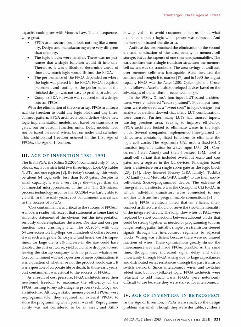
The Age of Invention ended with brutal attrition in the FPGA
business. A modern reader may not recognize most of the
companies or product names in Section III and in the FPGA
genealogical tree in Fig. 5 [6], [38]. Many of the companies
simply vanished. Others quietly sold their assets as theyexited the FPGA business. The cause of this attrition was
more than the normal market dynamics. There were impor-
tant changes in the technology, and those companies that did
not take advantage of the changes could not compete. Quan-
titative changes due to Moore’s Law resulted in qualitative
changes in the FPGAs built with semiconductor technology.
These changes characterized the Age of Expansion.
VI. AGE OF EXPANSION 1992–1999
Through the 1990s, Moore’s Law continued its rapid pace of
improvement, doubling transistor count every two years.
Pioneering the fabless business model, FPGA startup com-panies typically could not obtain leading-edge silicon tech-
nology in the early 1990s. As a result, FPGAs began the Age
of Expansion lagging the process introduction curve. In the
1990s, they became process leaders as the foundries realized
the value of using the FPGA as a process-driver application.
Foundries were able to build SRAM FPGAs as soon as they
were able to yield transistors and wires in a new technology.
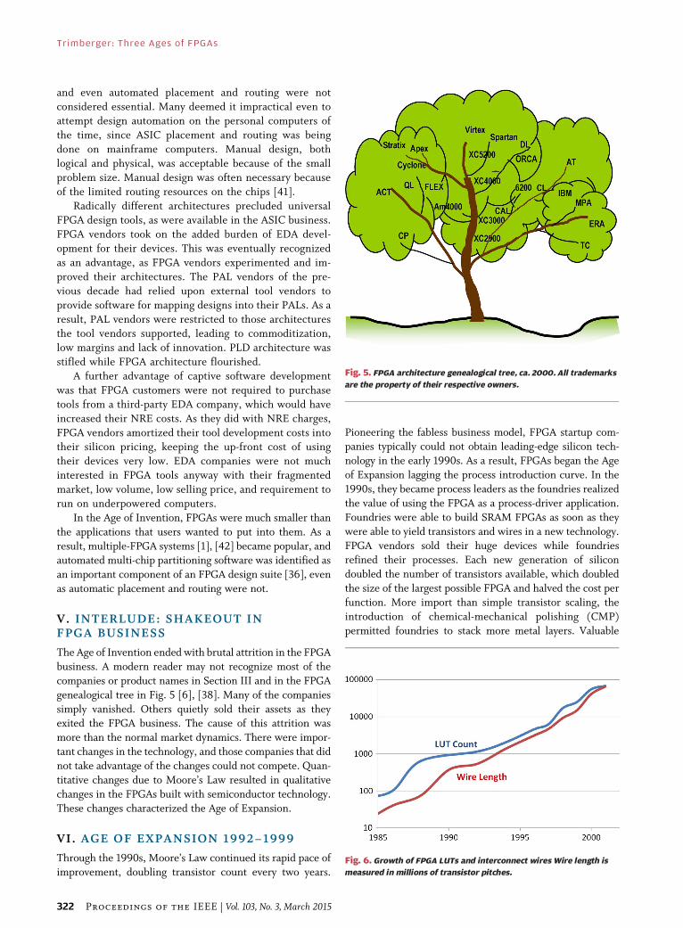
FPGA vendors sold their huge devices while foundriesrefined their processes. Each new generation of silicon
doubled the number of transistors available, which doubled
the size of the largest possible FPGA and halved the cost per
function. More import than simple transistor scaling, the
introduction of chemical-mechanical polishing (CMP)
permitted foundries to stack more metal layers. Valuable
Fig. 5. FPGA architecture genealogical tree, ca. 2000. All trademarks
are the property of their respective owners.
Fig. 6. Growth of FPGA LUTs and interconnect wires Wire length is
measured in millions of transistor pitches.
Trimberger: Three Ages of FPGAs
322 Proceedings of the IEEE | Vol. 103, No. 3, March 2015
for ASICs, this capability was explosive for FPGAs becausethe cost of valuable (nonbillable) interconnect dropped even
faster than the cost of transistors, and FPGA vendors
aggressively increased the interconnect on their devices to
accommodate the larger capacity (see Fig. 6).
This rapid process improvement had several effects
which we now examine.
A. Area Became Less PreciousNo one who joined the FPGA industry in the mid-1990s
would agree that cost was unimportant or area was not
precious. However, those who had experienced the ago-
nies of product development in the 1980s certainly saw the
difference. In the 1980s, transistor efficiency was neces-
sary in order to deliver any product whatsoever. In the
1990s, it was merely a matter of product definition. Area
was still important, but now it could be traded off forperformance, features and ease-of-use. The resulting de-
vices were less silicon efficient. This was unthinkable in
the Age of Invention just a few years earlier.
B. Design Automation Became EssentialIn the Age of Expansion, FPGA device capacity in-
creased rapidly as costs fell. FPGA applications became too
large for manual design. In 1992, the flagship XilinxXC4010 delivered a (claimed) maximum of 10 000 gates.
By 1999, the Virtex XCV1000 was rated at a million. In the
early 1990s, at the start of the Age of Expansion, automatic
placement and routing was preferred, but not entirely
trusted. By the end of the 1990s, automated synthesis [9],
placement and routing [3], [4], [19], [32], [37] were required
steps in the design process. Without the automation, the
design effort would be simply too great. The life of an FPGAcompany was now dependent upon the ability of design
automation tools to target the device. Those FPGA compa-
nies that controlled their software controlled their future.
Cheaper metal from process scaling led to more prog-
rammable interconnect wire, so that automated placement
tools could succeed with a less-precise placement.
Automated design tools required automation-friendly
architectures, architectures with regular and plentifulinterconnect resources to simplify algorithmic decision-
making. Cheaper wire also admitted longer wire segmen-
tation, interconnect wires that spanned multiple logic
blocks [2], [28], [44]. Wires spanning many blocks effec-
tively make physically distant logic logically closer, im-
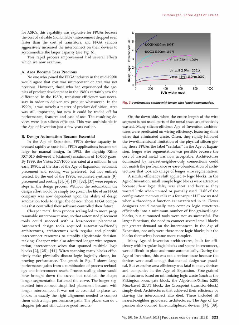
proving performance. The graph in Fig. 7 shows large
performance gains from a combination of process technol-
ogy and interconnect reach. Process scaling alone wouldhave brought down the curve, but retained the shape;
longer segmentation flattened the curve. The longer seg-
mented interconnect simplified placement because with
longer interconnect, it was not as essential to place two
blocks in exactly the right alignment needed to connect
them with a high performance path. The placer can do a
sloppier job and still achieve good results.
On the down side, when the entire length of the wire
segment is not used, parts of the metal trace are effectivelywasted. Many silicon-efficient Age of Invention architec-
tures were predicated on wiring efficiency, featuring short
wires that eliminated waste. Often, they rigidly followed
the two-dimensional limitation of the physical silicon giv-
ing those FPGAs the label ‘‘cellular.’’ In the Age of Expan-
sion, longer wire segmentation was possible because the
cost of wasted metal was now acceptable. Architectures
dominated by nearest-neighbor-only connections couldnot match the performance or ease-of-automation of archi-
tectures that took advantage of longer wire segmentation.
A similar efficiency shift applied to logic blocks. In the
Age of Invention, small, simple logic blocks were attractive
because their logic delay was short and because they
wasted little when unused or partially used. Half of the
configuration memory cells in a four-input LUT are wasted
when a three-input function is instantiated in it. Cleverdesigners could manually map complex logic structures
efficiently into a minimum number of fine-grained logic
blocks, but automated tools were not as successful. For
larger functions, the need to connect several small blocks
put greater demand on the interconnect. In the Age of
Expansion, not only were there more logic blocks, but the
blocks themselves became more complex.
Many Age of Invention architectures, built for effi-ciency with irregular logic blocks and sparse interconnect,
were difficult to place and route automatically. During the
Age of Invention, this was not a serious issue because the
devices were small enough that manual design was practi-
cal. But excessive area efficiency was fatal to many devices
and companies in the Age of Expansion. Fine-grained
architectures based on minimizing logic waste (such as the
Pilkington nand-gate block, the Algotronix/Xilinx 6200Mux-based 2LUT block, the Crosspoint transistor-block)
simply died. Architectures that achieved their efficiency by
starving the interconnect also died. These included all
nearest-neighbor grid-based architectures. The Age of Ex-
pansion also doomed time-multiplexed devices [14], [39],
Fig. 7. Performance scaling with longer wire length segmentation.
Trimberger: Three Ages of FPGAs
Vol. 103, No. 3, March 2015 | Proceedings of the IEEE 323
since equivalent capacity expansion could be had without theattendant complexity and performance loss by merely
waiting for the next process generation. The survivors in
the FPGA business were those that leveraged process
technology advancement to enable automation. Altera was
first, bringing the long-distance connections of their CPLDs
to the Altera FLEX architecture. FLEX was more automatable
than other FPGAs of the period that were dominated by short
wires. It achieved quick success. In the mid-1990s, AT&T/Lucent released ORCA [26] and Xilinx scaled up its XC4000
interconnect in number and length as it built larger devices.
The Age of Expansion was firmly established.
C. Emergence of SRAM as Technology of ChoiceOne aspect of the rapid progress of Moore’s Law was the
need to be on the forefront of process technology. The easiest
way to double the capacity and halve the cost for logic was totarget the next process technology node. This pressured
FPGA vendors to adopt leading-edge process technology.
FPGA companies using technologies that could not be easily
implemented on a new process were at a structural
disadvantage. This was the case with nonvolatile program-
mable technologies such as EPROM, Flash and antifuse.
When a new process technology becomes available, the first
components that are available are transistors and wires, theessential components of electronics. A static-memory-based
device could use a new, denser process immediately.
Antifuse devices were accurately promoted as being more
efficient on a particular technology node, but it took months
or years to qualify the antifuse on the new node. By the time
the antifuse was proven, SRAM FPGAs were already starting
to deliver on the next node. Antifuse technologies could not
keep pace with technology, so they needed to be twice asefficient as SRAM just to maintain product parity.
Antifuse devices suffered a second disadvantage: lack
of reprogrammability. As customers grew accustomed to
‘‘volatile’’ SRAM FPGAs, they began to appreciate the ad-
vantages of in-system programmability and field-updating
of hardware. In contrast, a one-time-programmable device
needed to be physically handled to be updated or to re-
medy design errors. The alternative for antifuse deviceswas an extensive ASIC-like verification phase, which un-
dermined the value of the FPGA.
The rapid pace of Moore’s Law in the Age of Expansion
relegated antifuse and flash FPGAs to niche products.
D. Emergence of LUT as Logic Cell of ChoiceLUTs survived and dominated despite their docu-
mented inefficiency in the Age of Expansion for severalreasons. First, LUT-based architectures were easy targets
for synthesis tools. This statement would have been dis-
puted in the mid-1990s, when synthesis vendors com-
plained that FPGAs were not ‘‘synthesis friendly.’’ This
perception arose because synthesis tools were initially de-
veloped to target ASICs. Their technology mappers ex-
pected a small library in which each cell was described as a
network of nands with inverters. Since a LUT implementsany of the 22n
combinations of its inputs, a complete library
would have been enormous. ASIC technology mappers did
a poor job on LUT-based FPGAs. But by the mid-1990s,
targeted LUT mappers exploited the simplicity of mapping
arbitrary functions into LUTs [9].
The LUT has hidden efficiencies. A LUT is a memory,
and memories lay out efficiently in silicon. The LUT also
saves interconnect. FPGA programmable interconnect isexpensive in area and delay. Rather than a simple metal
wire as in an ASIC, FPGA interconnect contains buffers,
routing multiplexers and the memory cells to control them.
Therefore, much more of the cost of the logic is actually in
the interconnect [15]. Since a LUT implements any func-
tion of its inputs, automation tools need only route the
desired signals together at a LUT in order to retire the
function of those inputs. There was no need to make mul-tiple levels of LUTs just to create the desired function of a
small set of inputs. LUT input pins are arbitrarily swappa-
ble, so the router need not target a specific pin. As a result,
LUT-based logic reduced the amount of interconnect re-
quired to implement a function. With good synthesis, the
waste from unused LUT functionality was less than the
savings from the reduced interconnect requirement.
Distributed-memory-cell programming permitted archi-tectural freedom and gave FPGA vendors nearly universal
access to process technology. LUTs for logic implementation
eased the burden on interconnect. Xilinx-derived LUT-based
architectures appeared at Xilinx second sources: Monolithic
Memories, AMD and AT&T. In the Age of Expansion, other
companies, notably Altera, and AT&T/Lucent, adopted
memory cell and LUT architectures as well.
VII. INTERLUDE: FPGA CAPACITYBELL CURVE
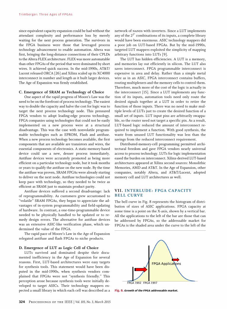
The bell curve in Fig. 8 represents the histogram of distri-
bution of sizes of ASIC applications. FPGA capacity at
some time is a point on the X-axis, shown by a vertical bar.
All the applications to the left of the bar are those that can
be addressed by FPGAs, so the addressable market for
FPGAs is the shaded area under the curve to the left of the
Fig. 8. Growth of the FPGA addressable market.
Trimberger: Three Ages of FPGAs
324 Proceedings of the IEEE | Vol. 103, No. 3, March 2015
bar. During the Age of Expansion, FPGA capacity in-
creased at Moore’s Law pace, so the bar moved to the right.
Of course, the entire bell curve of applications also movedto the right, but the rate of growth in application size was
slower than the FPGA capacity growth. As a result, the bar
representing FPGAs moved quickly to the right relative to
the distribution of designs. Since FPGAs were addressing
the low end of the curve, even a small increase in available
capacity admitted a large number of new applications.
During the Age of Expansion, FPGA capacity covered a
growing fraction of extant designs and grew to address themajority of ASIC applications.
This increasing applicability can also be seen from the
‘‘Design Gap’’ slide popular with EDA vendors in the late
1990s (Fig. 9). The capacity of ASICs and FPGAs grew with
Moore’s Law: ASICs growing at a 59% annual growth rate,
and FPGAs at 48% annual growth rate. The observed aver-
age ASIC design start grew considerably more slowly, only
25% per year. As a result, FPGA capacity met the averageASIC design size in 2000, though for a large (expensive)
FPGA. By 2004, though, a ten-dollar FPGA was predicted to
meet the average ASIC requirement. That crossover point
moved farther out in the early 2000s as FPGAs addressed
the low end of the ASIC market and those small designs
became FPGA designs. Small designs were no longer in-
cluded in the average ASIC design size calculation, thereby
inflating the average ASIC design size in the new mille-nnium. Today, the average ASIC is much larger than Fig. 9
would suggest, because FPGAs successfully absorbed nearly
the entire low-end of the ASIC business.
VIII . AGE OF EXPANSIONIN RETROSPECT
Through the Age of Expansion, Moore’s Law rapidly in-
creased the capacity of FPGAs, leading to a demand for
design automation and permitting longer interconnect
segmentation. Overly efficient architectures that could not
be effectively automated simply disappeared. SRAM de-vices were first to exploit new process technology and
dominated the business. FPGAs encroached on ASIC terri-
tory as FPGA device capacity grew more rapidly than the
demand from applications. No longer did users clamor for
multi-FPGA partitioning software: designs fit, sometimes
snugly, into the available FPGAs.
As FPGAs became more popular, EDA companies be-
came interested in providing tools for them. However,overtures by EDA companies were viewed with suspicion.
FPGA veterans had seen how PLD vendors had lost control
over their innovation by surrendering the software. They
refused to let that happen in the FPGA domain. Further,
the major FPGA companies feared their customers could
become dependent upon an external EDA company’s tools.
If that happened, the EDA company could effectively drive
up the FPGA NRE by their software tools prices. Thiswould undermine the FPGA value proposition, shifting the
crossover point back to lower volume. Some important
FPGA-EDA alliances were made in the synthesis domainVan arms-length from the physical design tools that defined
the architecture. Despite the alliances, the FPGA compa-
nies maintained competitive projects to prevent the pos-
sibility of dependence. In the Age of Expansion, FPGA
vendors found themselves competing against both ASICtechnology and EDA technology.
IX. INTERLUDE: XILINX MARKETING,CA. 2000
By the late 1990s, the Age of Expansion was well under-
stood in the FPGA business. FPGA vendors were aggres-
sively pursuing process technology as the solution to theirsize, performance and capacity issues. Each new process
generation brought with it numerous new applications.
The slide in Fig. 10 is excerpted from a Xilinx marketing
Fig. 9. Design gap. Source: Data: Synopsys, Gartner Dataquest,
VLSI Technology, Xilinx.
Fig. 10. Xilinx marketing ca. 2000 Image courtesy of Xilinx.
Trimberger: Three Ages of FPGAs
Vol. 103, No. 3, March 2015 | Proceedings of the IEEE 325
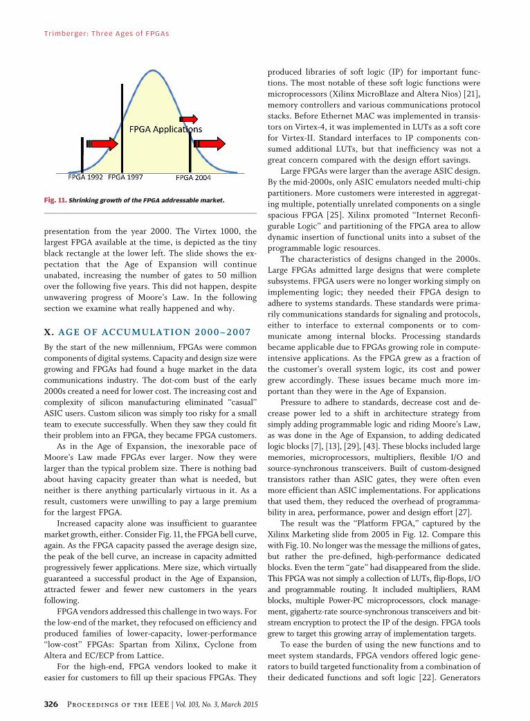
presentation from the year 2000. The Virtex 1000, thelargest FPGA available at the time, is depicted as the tiny
black rectangle at the lower left. The slide shows the ex-
pectation that the Age of Expansion will continue
unabated, increasing the number of gates to 50 million
over the following five years. This did not happen, despite
unwavering progress of Moore’s Law. In the following
section we examine what really happened and why.
X. AGE OF ACCUMULATION 2000–2007
By the start of the new millennium, FPGAs were common
components of digital systems. Capacity and design size were
growing and FPGAs had found a huge market in the data
communications industry. The dot-com bust of the early
2000s created a need for lower cost. The increasing cost and
complexity of silicon manufacturing eliminated ‘‘casual’’
ASIC users. Custom silicon was simply too risky for a small
team to execute successfully. When they saw they could fittheir problem into an FPGA, they became FPGA customers.
As in the Age of Expansion, the inexorable pace of
Moore’s Law made FPGAs ever larger. Now they were
larger than the typical problem size. There is nothing bad
about having capacity greater than what is needed, but
neither is there anything particularly virtuous in it. As a
result, customers were unwilling to pay a large premium
for the largest FPGA.Increased capacity alone was insufficient to guarantee
market growth, either. Consider Fig. 11, the FPGA bell curve,
again. As the FPGA capacity passed the average design size,
the peak of the bell curve, an increase in capacity admitted
progressively fewer applications. Mere size, which virtually
guaranteed a successful product in the Age of Expansion,
attracted fewer and fewer new customers in the years
following.FPGA vendors addressed this challenge in two ways. For
the low-end of the market, they refocused on efficiency and
produced families of lower-capacity, lower-performance
‘‘low-cost’’ FPGAs: Spartan from Xilinx, Cyclone from
Altera and EC/ECP from Lattice.
For the high-end, FPGA vendors looked to make it
easier for customers to fill up their spacious FPGAs. They
produced libraries of soft logic (IP) for important func-tions. The most notable of these soft logic functions were
microprocessors (Xilinx MicroBlaze and Altera Nios) [21],
memory controllers and various communications protocol
stacks. Before Ethernet MAC was implemented in transis-
tors on Virtex-4, it was implemented in LUTs as a soft core
for Virtex-II. Standard interfaces to IP components con-
sumed additional LUTs, but that inefficiency was not a
great concern compared with the design effort savings.Large FPGAs were larger than the average ASIC design.
By the mid-2000s, only ASIC emulators needed multi-chip
partitioners. More customers were interested in aggregat-
ing multiple, potentially unrelated components on a single
spacious FPGA [25]. Xilinx promoted ‘‘Internet Reconfi-
gurable Logic’’ and partitioning of the FPGA area to allow
dynamic insertion of functional units into a subset of the
programmable logic resources.The characteristics of designs changed in the 2000s.
Large FPGAs admitted large designs that were complete
subsystems. FPGA users were no longer working simply on
implementing logic; they needed their FPGA design to
adhere to systems standards. These standards were prima-
rily communications standards for signaling and protocols,
either to interface to external components or to com-
municate among internal blocks. Processing standardsbecame applicable due to FPGAs growing role in compute-
intensive applications. As the FPGA grew as a fraction of
the customer’s overall system logic, its cost and power
grew accordingly. These issues became much more im-
portant than they were in the Age of Expansion.
Pressure to adhere to standards, decrease cost and de-
crease power led to a shift in architecture strategy from
simply adding programmable logic and riding Moore’s Law,as was done in the Age of Expansion, to adding dedicated
logic blocks [7], [13], [29], [43]. These blocks included large
memories, microprocessors, multipliers, flexible I/O and
source-synchronous transceivers. Built of custom-designed
transistors rather than ASIC gates, they were often even
more efficient than ASIC implementations. For applications
that used them, they reduced the overhead of programma-
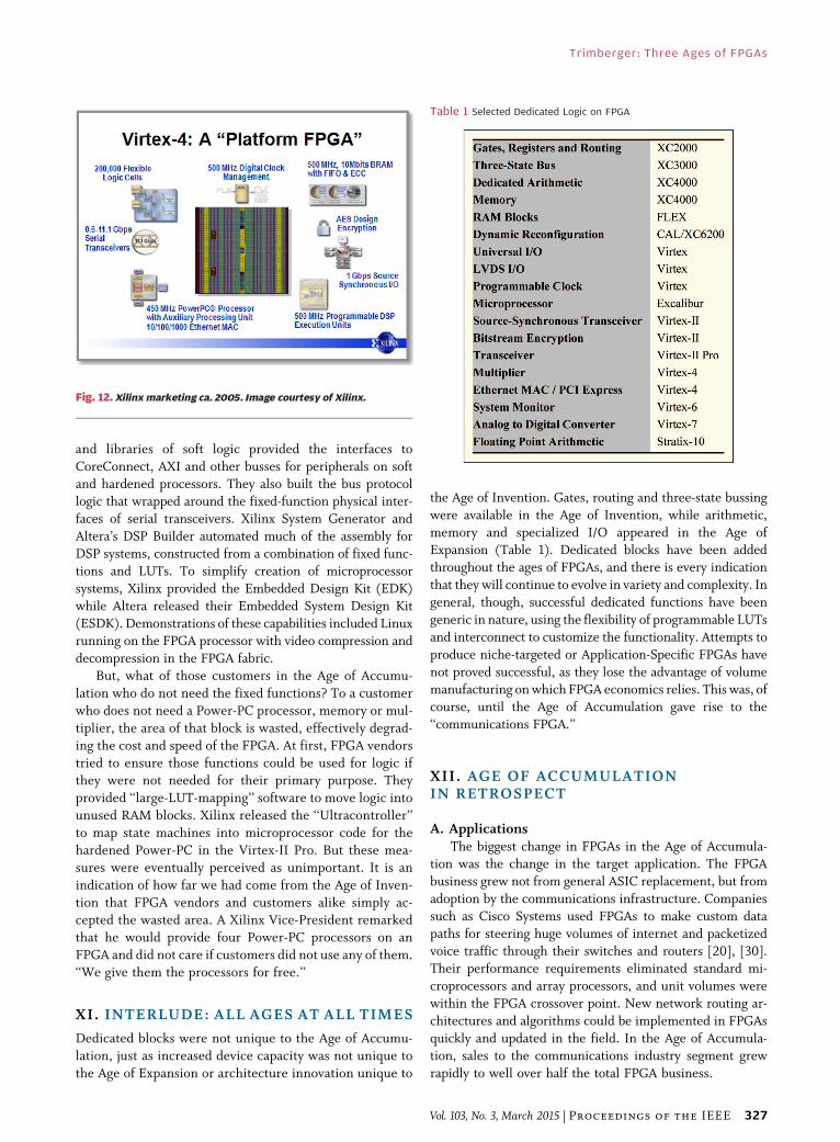
bility in area, performance, power and design effort [27].The result was the ‘‘Platform FPGA,’’ captured by the
Xilinx Marketing slide from 2005 in Fig. 12. Compare this
with Fig. 10. No longer was the message the millions of gates,
but rather the pre-defined, high-performance dedicated
blocks. Even the term ‘‘gate’’ had disappeared from the slide.
This FPGA was not simply a collection of LUTs, flip-flops, I/O
and programmable routing. It included multipliers, RAM
blocks, multiple Power-PC microprocessors, clock manage-ment, gigahertz-rate source-synchronous transceivers and bit-
stream encryption to protect the IP of the design. FPGA tools
grew to target this growing array of implementation targets.
To ease the burden of using the new functions and to
meet system standards, FPGA vendors offered logic gene-
rators to build targeted functionality from a combination of
their dedicated functions and soft logic [22]. Generators
Fig. 11. Shrinking growth of the FPGA addressable market.
Trimberger: Three Ages of FPGAs
326 Proceedings of the IEEE | Vol. 103, No. 3, March 2015
and libraries of soft logic provided the interfaces to
CoreConnect, AXI and other busses for peripherals on soft
and hardened processors. They also built the bus protocollogic that wrapped around the fixed-function physical inter-
faces of serial transceivers. Xilinx System Generator and
Altera’s DSP Builder automated much of the assembly for
DSP systems, constructed from a combination of fixed func-
tions and LUTs. To simplify creation of microprocessor
systems, Xilinx provided the Embedded Design Kit (EDK)
while Altera released their Embedded System Design Kit
(ESDK). Demonstrations of these capabilities included Linuxrunning on the FPGA processor with video compression and
decompression in the FPGA fabric.
But, what of those customers in the Age of Accumu-
lation who do not need the fixed functions? To a customer
who does not need a Power-PC processor, memory or mul-
tiplier, the area of that block is wasted, effectively degrad-
ing the cost and speed of the FPGA. At first, FPGA vendors
tried to ensure those functions could be used for logic ifthey were not needed for their primary purpose. They
provided ‘‘large-LUT-mapping’’ software to move logic into
unused RAM blocks. Xilinx released the ‘‘Ultracontroller’’
to map state machines into microprocessor code for the
hardened Power-PC in the Virtex-II Pro. But these mea-
sures were eventually perceived as unimportant. It is an
indication of how far we had come from the Age of Inven-
tion that FPGA vendors and customers alike simply ac-cepted the wasted area. A Xilinx Vice-President remarked
that he would provide four Power-PC processors on an
FPGA and did not care if customers did not use any of them.
‘‘We give them the processors for free.’’
XI. INTERLUDE: ALL AGES AT ALL TIMES
Dedicated blocks were not unique to the Age of Accumu-
lation, just as increased device capacity was not unique to
the Age of Expansion or architecture innovation unique to
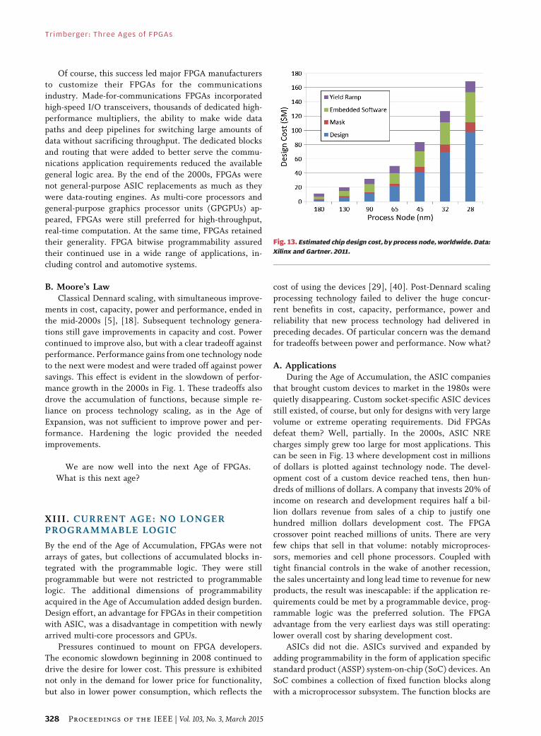
the Age of Invention. Gates, routing and three-state bussing
were available in the Age of Invention, while arithmetic,
memory and specialized I/O appeared in the Age ofExpansion (Table 1). Dedicated blocks have been added
throughout the ages of FPGAs, and there is every indication
that they will continue to evolve in variety and complexity. In
general, though, successful dedicated functions have been
generic in nature, using the flexibility of programmable LUTs
and interconnect to customize the functionality. Attempts to
produce niche-targeted or Application-Specific FPGAs have
not proved successful, as they lose the advantage of volumemanufacturing on which FPGA economics relies. This was, of
course, until the Age of Accumulation gave rise to the
‘‘communications FPGA.’’
XII. AGE OF ACCUMULATIONIN RETROSPECT
A. ApplicationsThe biggest change in FPGAs in the Age of Accumula-
tion was the change in the target application. The FPGA
business grew not from general ASIC replacement, but from
adoption by the communications infrastructure. Companies
such as Cisco Systems used FPGAs to make custom data
paths for steering huge volumes of internet and packetized
voice traffic through their switches and routers [20], [30].Their performance requirements eliminated standard mi-
croprocessors and array processors, and unit volumes were
within the FPGA crossover point. New network routing ar-
chitectures and algorithms could be implemented in FPGAs
quickly and updated in the field. In the Age of Accumula-
tion, sales to the communications industry segment grew
rapidly to well over half the total FPGA business.
Fig. 12. Xilinx marketing ca. 2005. Image courtesy of Xilinx.
Table 1 Selected Dedicated Logic on FPGA
Trimberger: Three Ages of FPGAs
Vol. 103, No. 3, March 2015 | Proceedings of the IEEE 327
Of course, this success led major FPGA manufacturersto customize their FPGAs for the communications
industry. Made-for-communications FPGAs incorporated
high-speed I/O transceivers, thousands of dedicated high-
performance multipliers, the ability to make wide data
paths and deep pipelines for switching large amounts of
data without sacrificing throughput. The dedicated blocks
and routing that were added to better serve the commu-
nications application requirements reduced the availablegeneral logic area. By the end of the 2000s, FPGAs were
not general-purpose ASIC replacements as much as they
were data-routing engines. As multi-core processors and
general-purpose graphics processor units (GPGPUs) ap-
peared, FPGAs were still preferred for high-throughput,
real-time computation. At the same time, FPGAs retained
their generality. FPGA bitwise programmability assured
their continued use in a wide range of applications, in-cluding control and automotive systems.
B. Moore’s LawClassical Dennard scaling, with simultaneous improve-
ments in cost, capacity, power and performance, ended in
the mid-2000s [5], [18]. Subsequent technology genera-
tions still gave improvements in capacity and cost. Power
continued to improve also, but with a clear tradeoff againstperformance. Performance gains from one technology node
to the next were modest and were traded off against power
savings. This effect is evident in the slowdown of perfor-
mance growth in the 2000s in Fig. 1. These tradeoffs also
drove the accumulation of functions, because simple re-
liance on process technology scaling, as in the Age of
Expansion, was not sufficient to improve power and per-
formance. Hardening the logic provided the neededimprovements.
We are now well into the next Age of FPGAs.
What is this next age?
XIII. CURRENT AGE: NO LONGERPROGRAMMABLE LOGIC
By the end of the Age of Accumulation, FPGAs were not
arrays of gates, but collections of accumulated blocks in-
tegrated with the programmable logic. They were still
programmable but were not restricted to programmable
logic. The additional dimensions of programmability
acquired in the Age of Accumulation added design burden.
Design effort, an advantage for FPGAs in their competitionwith ASIC, was a disadvantage in competition with newly
arrived multi-core processors and GPUs.
Pressures continued to mount on FPGA developers.
The economic slowdown beginning in 2008 continued to
drive the desire for lower cost. This pressure is exhibited
not only in the demand for lower price for functionality,
but also in lower power consumption, which reflects the
cost of using the devices [29], [40]. Post-Dennard scaling
processing technology failed to deliver the huge concur-
rent benefits in cost, capacity, performance, power and
reliability that new process technology had delivered in
preceding decades. Of particular concern was the demand
for tradeoffs between power and performance. Now what?
A. ApplicationsDuring the Age of Accumulation, the ASIC companies
that brought custom devices to market in the 1980s were
quietly disappearing. Custom socket-specific ASIC devices
still existed, of course, but only for designs with very large
volume or extreme operating requirements. Did FPGAs
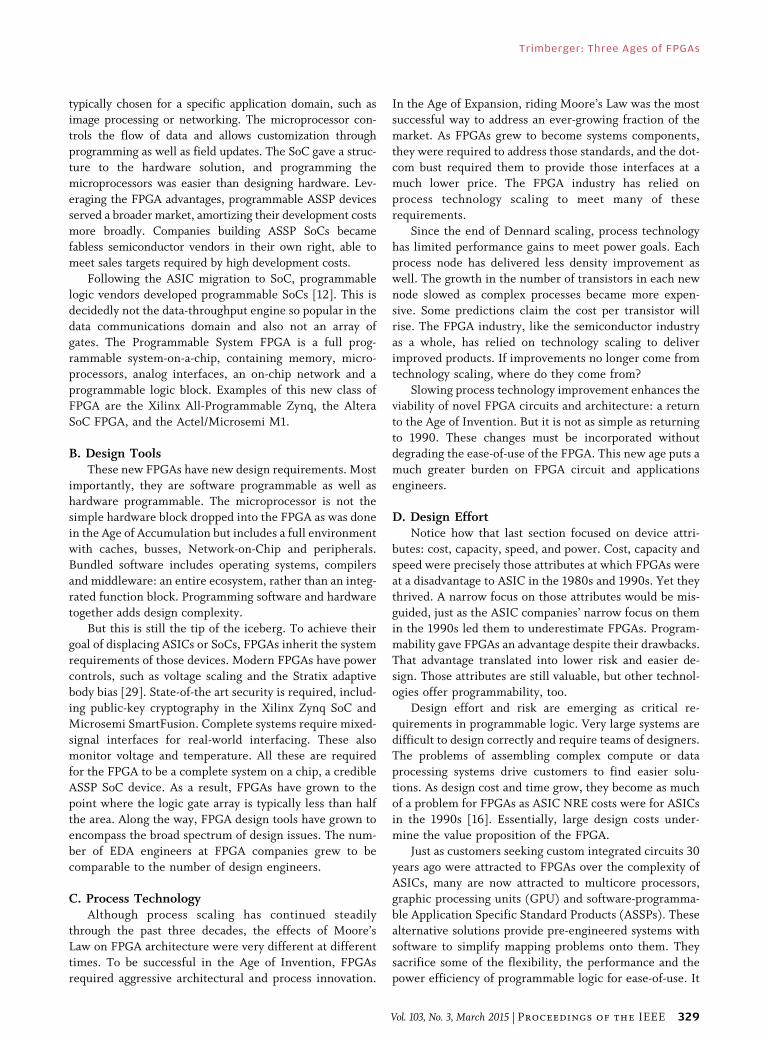
defeat them? Well, partially. In the 2000s, ASIC NREcharges simply grew too large for most applications. This
can be seen in Fig. 13 where development cost in millions
of dollars is plotted against technology node. The devel-
opment cost of a custom device reached tens, then hun-
dreds of millions of dollars. A company that invests 20% of
income on research and development requires half a bil-
lion dollars revenue from sales of a chip to justify one
hundred million dollars development cost. The FPGAcrossover point reached millions of units. There are very
few chips that sell in that volume: notably microproces-
sors, memories and cell phone processors. Coupled with
tight financial controls in the wake of another recession,
the sales uncertainty and long lead time to revenue for new
products, the result was inescapable: if the application re-
quirements could be met by a programmable device, prog-
rammable logic was the preferred solution. The FPGAadvantage from the very earliest days was still operating:
lower overall cost by sharing development cost.
ASICs did not die. ASICs survived and expanded by
adding programmability in the form of application specific
standard product (ASSP) system-on-chip (SoC) devices. An
SoC combines a collection of fixed function blocks along
with a microprocessor subsystem. The function blocks are
Fig. 13. Estimated chip design cost, by process node, worldwide. Data:
Xilinx and Gartner. 2011.
Trimberger: Three Ages of FPGAs
328 Proceedings of the IEEE | Vol. 103, No. 3, March 2015
typically chosen for a specific application domain, such asimage processing or networking. The microprocessor con-
trols the flow of data and allows customization through
programming as well as field updates. The SoC gave a struc-
ture to the hardware solution, and programming the
microprocessors was easier than designing hardware. Lev-
eraging the FPGA advantages, programmable ASSP devices
served a broader market, amortizing their development costs
more broadly. Companies building ASSP SoCs becamefabless semiconductor vendors in their own right, able to
meet sales targets required by high development costs.
Following the ASIC migration to SoC, programmable
logic vendors developed programmable SoCs [12]. This is
decidedly not the data-throughput engine so popular in the
data communications domain and also not an array of
gates. The Programmable System FPGA is a full prog-
rammable system-on-a-chip, containing memory, micro-processors, analog interfaces, an on-chip network and a
programmable logic block. Examples of this new class of
FPGA are the Xilinx All-Programmable Zynq, the Altera
SoC FPGA, and the Actel/Microsemi M1.
B. Design ToolsThese new FPGAs have new design requirements. Most
importantly, they are software programmable as well ashardware programmable. The microprocessor is not the
simple hardware block dropped into the FPGA as was done
in the Age of Accumulation but includes a full environment
with caches, busses, Network-on-Chip and peripherals.
Bundled software includes operating systems, compilers
and middleware: an entire ecosystem, rather than an integ-
rated function block. Programming software and hardware
together adds design complexity.But this is still the tip of the iceberg. To achieve their
goal of displacing ASICs or SoCs, FPGAs inherit the system
requirements of those devices. Modern FPGAs have power
controls, such as voltage scaling and the Stratix adaptive
body bias [29]. State-of-the art security is required, includ-
ing public-key cryptography in the Xilinx Zynq SoC and
Microsemi SmartFusion. Complete systems require mixed-
signal interfaces for real-world interfacing. These alsomonitor voltage and temperature. All these are required
for the FPGA to be a complete system on a chip, a credible
ASSP SoC device. As a result, FPGAs have grown to the
point where the logic gate array is typically less than half
the area. Along the way, FPGA design tools have grown to
encompass the broad spectrum of design issues. The num-
ber of EDA engineers at FPGA companies grew to be
comparable to the number of design engineers.
C. Process TechnologyAlthough process scaling has continued steadily
through the past three decades, the effects of Moore’s
Law on FPGA architecture were very different at different
times. To be successful in the Age of Invention, FPGAs
required aggressive architectural and process innovation.
In the Age of Expansion, riding Moore’s Law was the mostsuccessful way to address an ever-growing fraction of the
market. As FPGAs grew to become systems components,
they were required to address those standards, and the dot-
com bust required them to provide those interfaces at a
much lower price. The FPGA industry has relied on
process technology scaling to meet many of these
requirements.
Since the end of Dennard scaling, process technologyhas limited performance gains to meet power goals. Each
process node has delivered less density improvement as
well. The growth in the number of transistors in each new
node slowed as complex processes became more expen-
sive. Some predictions claim the cost per transistor will
rise. The FPGA industry, like the semiconductor industry
as a whole, has relied on technology scaling to deliver
improved products. If improvements no longer come fromtechnology scaling, where do they come from?
Slowing process technology improvement enhances the
viability of novel FPGA circuits and architecture: a return
to the Age of Invention. But it is not as simple as returning
to 1990. These changes must be incorporated without
degrading the ease-of-use of the FPGA. This new age puts a
much greater burden on FPGA circuit and applications
engineers.
D. Design EffortNotice how that last section focused on device attri-
butes: cost, capacity, speed, and power. Cost, capacity and
speed were precisely those attributes at which FPGAs were
at a disadvantage to ASIC in the 1980s and 1990s. Yet they
thrived. A narrow focus on those attributes would be mis-
guided, just as the ASIC companies’ narrow focus on themin the 1990s led them to underestimate FPGAs. Program-
mability gave FPGAs an advantage despite their drawbacks.
That advantage translated into lower risk and easier de-
sign. Those attributes are still valuable, but other technol-
ogies offer programmability, too.
Design effort and risk are emerging as critical re-
quirements in programmable logic. Very large systems are
difficult to design correctly and require teams of designers.The problems of assembling complex compute or data
processing systems drive customers to find easier solu-
tions. As design cost and time grow, they become as much
of a problem for FPGAs as ASIC NRE costs were for ASICs
in the 1990s [16]. Essentially, large design costs under-
mine the value proposition of the FPGA.
Just as customers seeking custom integrated circuits 30
years ago were attracted to FPGAs over the complexity ofASICs, many are now attracted to multicore processors,
graphic processing units (GPU) and software-programma-
ble Application Specific Standard Products (ASSPs). These
alternative solutions provide pre-engineered systems with
software to simplify mapping problems onto them. They
sacrifice some of the flexibility, the performance and the
power efficiency of programmable logic for ease-of-use. It
Trimberger: Three Ages of FPGAs
Vol. 103, No. 3, March 2015 | Proceedings of the IEEE 329
is clear that, while there are many FPGA users who need toexploit the limits of FPGA technology, there are many
others for whom the technological capability is adequate,
but who are daunted by the complexity of using that
technology.
The complexity and capability of devices have driven an
increase in capability of design tools. Modern FPGA tool-
sets include high-level synthesis compilation from C, Cuda
and OpenCL to logic or to embedded microprocessors [10],[11], [35]. Vendor-provided libraries of logic and process-
ing functions defray design costs. Working operating sys-
tems and hypervisors control FPGA SoC operation. Team
design functions, including build control, are built into
FPGA design systems. Some capabilities are built by the
vendors themselves, others are part of the growing FPGA
ecosystem.
Clearly, usability is critical to this next age of FPGAs.Will that usability be realized through better tools, novel
architectures, exploitation of the process technology, orgreater accumulation of fixed blocks? Most likely, just as
every previous age was required to contribute to each suc-
cessive age, all techniques will be needed to succeed. And
more besides. As with the other Ages, the next Age of
FPGAs will only be completely clear in retrospect.
Throughout the age, expect to see time-honored good
engineering: producing the best products possible from the
available technology. This good engineering will beaccomplished as the available technology and the definition
of ‘‘best’’ continuously change.
XIV. FUTURE AGE OF FPGAS
What of the future? What is the age after this one? I refuse
to speculate, but instead issue a challenge: remember the
words of Alan Kay, ‘‘The best way to predict the future is toinvent it.’’ h
REF ERENCE S
[1] J. Babb et al., ‘‘Logic emulation withvirtual wires,’’ IEEE J. Comput. AidedDesign Circuits Syst., vol. 16, no. 6,pp. 609–626, Jun. 1997.
[2] V. Betz and J. Rose, ‘‘FPGA routingarchitecture: Segmentation andbuffering to optimize speed anddensity,’’ in Proc. FPGA ’99, ACM Symp.FPGAs, pp. 59–68.
[3] V. Betz, J. Rose, and A. Marquardt,Architecture and CAD for Deep-SubmicronFPGAs. Boston, MA, USA: KluwerAcademic, Feb. 1999.
[4] V. Betz and J. Rose, ‘‘VPR: A newpacking, placement and routing toolfor FPGA Research,’’ in Proc. Int.Workshop Field Program. Logic Appl.,1997, pp. 213–222.
[5] M. Bohr, ‘‘A 30 year retrospective onDennard’s MOSFET scaling paper,’’IEEE Solid-State Circuits Soc. Newslett.,vol. 12, no. 1, pp. 11–13, 2007.
[6] S. Brown and J. Rose, ‘‘FPGA and CPLDArchitectures: A tutorial,’’ IEEE DesignTest Comput., vol. 13, no. 2, pp. 32–57,1996.
[7] T. Callahan, J. Hauser, and J. Wawrzynek,‘‘The Garp architecture and C compiler,’’IEEE Computer, 2000.
[8] W. Carter, K. Duong, R. H. Freeman,H. Hsieh, J. Y. Ja, J. E. Mahoney, L. T. Ngo,and S. L. Sze, ‘‘A user programmablereconfigurable gate array,’’ in Proc. CustomIntegr. Circuits Conf., 1986, pp. 233–235.
[9] J. Cong and Y. Ding, ‘‘An optimal technologymapping algorithm for delay optimizationin lookup-table FPGA designs,’’ IEEETrans. Comput. Aided Design Circuits Syst.,vol. 13, no. 1, Jan. 1994.
[10] J. Cong et al., ‘‘High-level synthesis forFPGAs: From prototyping to deployment,’’IEEE Trans. Comput.-Aided Design CircuitsSyst., vol. 30, no. 4, Apr. 2011.
[11] T. S. Czajkowski et al., ‘‘From OpenCL tohigh-performance hardware on FPGAs,’’ inProc. Int. Conf. Field Program. Logic Appl.(FPL), 2012, pp. 531–534.
[12] L. Crockett, R. Elliot, M. A. Enderwitz, andR. W. Stewart, The Zynq Book, StrathclydeAcademic, 2014.
[13] A. deHon, ‘‘DPGA-coupled microprocessors:Commodity ICs for the Early 21st Century,’’ inProc. IEEE FCCM, 1994, pp. 31–39.
[14] A. deHon, ‘‘DPGA utilization and application,’’in Proc. FPGA, 1996, pp. 115–121.
[15] A. deHon, ‘‘Balancing interconnect andcomputation in a reconfigurable computingarray (or, why you don’t really want100% LUT utilization),’’ in Proc. Int. Symp.Field Program. Gate Arrays, Feb. 1999,pp. 125–134.
[16] P. Dworksy. (2012). How can we keep ourFPGAs from falling into the productivitygap. Design and Reuse, viewed Sep. 16, 2014.Available: http://www.slideshare.net/designreuse/111207-ip-so-c-dworskyfpga-panel-slides
[17] K. El-Ayat et al., ‘‘A CMOS electricallyconfigurable gate array,’’ IEEE J. Solid-StateCircuits, vol. 24, no. 3, pp. 752–762,Mar. 1989.
[18] H. Esmaeilzadeh, E. Blem, R. St.Amant,K. Sankaralingam, and D. Burger,‘‘Dark silicon and the end of multicorescaling,’’ in Proc. ISCA 2011, pp. 365–376.
[19] J. Frankle, ‘‘Iterative and adaptive slackallocation for performance-driven layoutand FPGA routing,’’ in Proc. IEEE DesignAutom. Conf., 1992, pp. 536–542.
[20] G. Gibb, J. W. Lockwood, J. Naous, P. Hartke,and N. McKeown, ‘‘NetFPGA: An openplatform for teaching how to build gigabit-ratenetwork switches and routers,’’ IEEE J. Educ.,vol. 51, no. 3, pp. 364–369, Aug. 2008.
[21] T. Halfhill, ‘‘Microblaze v7 Gets an MMU,’’Microprocessor Rep., Nov. 13, 2007.
[22] J. Hwang and J. Ballagh, ‘‘Building customFIR filters using system generator,’’ inField-Programmable Logic and Applications:Reconfigurable Computing is Going Mainstream,Lecture Notes in Computer Science, M. Glesner,P. Zipf, and M. Renovell, Eds. New York,NY, USA: Springer, 2002, pp. 1101–1104.
[23] G. Jones and D. M. Wedgewood, ‘‘An effectivehardware/software solution for fine grainedarchitectures,’’ in Proc. FPGA, 1994.
[24] T. Kean, ‘‘Configurable Logic: A dynamicallyprogrammable cellular architecture and itsVLSI implementation,’’ Ph.D. dissertationCST62-89, Dept. Comput. Sci., Univ.Edinburgh, Edinburgh, U.K.
[25] C. Koo, ‘‘Benefits of partial reconfiguration,’’in Xcell, Fourth Quarter 2005, Xilinx.
[26] R. H. Krambeck, C.-T. Chen, and R. Y. Tsui,‘‘ORCA: A high speed, high density FPGAarchitecture,’’ in Dig. Papers Compcon Spring’93, 1993, pp. 367–372.
[27] I. Kuon and J. Rose, ‘‘Measuring the gapbetween FPGAs and ASICs,’’ IEEE J. Comput.Aided Design Circuits Syst., vol. 26, no. 2,2007.
[28] D. Lewis et al., ‘‘The Stratix-II logic androuting architecture,’’ in Proc. FPGA,2003.
[29] D. Lewis et al., ‘‘Architectural enhancementsin Stratix-III and Stratix-IV,’’ in Proc. ACM/SIGDA Int. Symp. Field Programmable GateArrays, ACM, 2009, pp. 33–42.
[30] J. W. Lockwood, N. Naufel, J. S. Turner, andD. E. Taylor, ‘‘Reprogrammable networkpacket processing on the field programmableport extender (FPX),’’ in Proc. ISFPGA 2001,ACM, pp. 87–93.
[31] D. J. Marple, ‘‘An MPGA-like FPGA,’’ IEEEDesign Test Comput., vol. 9, no. 4, 1989.
[32] L. McMurchie and C. Ebeling, ‘‘PathFinder:A negotiation-based performance-drivenrouter for FPGAs,’’ in Proc. FPGA ’95,ACM.
[33] G. Moore, ‘‘Are we really ready for VLSI?’’in Proc. Caltech Conf. Very Large Scale Integr.,1979.
[34] H. Muroga et al., ‘‘A large Scale FPGAwith 10 K core cells with CMOS 0.8 um3-layered metal process,’’ in Proc. CICC,1991.
[35] A. Papakonstantinou et al., ‘‘FCUDA:Enabling efficient compilation of CUDAkernels onto FPGAs,’’ in Proc. IEEE 7thInt. Symp. Appl.-Specific Processors (SASP),2009.
[36] K. Roy and C. Sechen, ‘‘A timing-drivenN-way multi-chip partitioner,’’ in Proc.IEEE ICCAD, 1993, pp. 240–247.
[37] V. P. Roychowdhury, J. W. Greene, andA. El-Gamal, ‘‘Segmented channel routing,’’Trans. Computer-Aided Design Integ.Circuits Syst., vol. 12, no. 1, pp. 79–95,1993.
[38] S. Trimberger, Ed., Field ProgrammableGate Array Technology. Boston, MA, USA:Kluwer Academic, 1994.
Trimberger: Three Ages of FPGAs
330 Proceedings of the IEEE | Vol. 103, No. 3, March 2015
[39] S. Trimberger, R. Carberry, A. Johnson, andJ. Wong, ‘‘A time-multiplexed FPGA,’’ in Proc.FCCM, 1997.
[40] T. Tuan, A. Rahman, S. Das, S. Trimberger,and S. Kao, ‘‘A 90-nm low-power FPGAfor battery-powered applications,’’ IEEETrans. Comput. Aided Design Circuits Syst.,vol. 26, no. 2, 2007.
[41] B. von Herzen, ‘‘Signal processing at250 MHz using high-performanceFPGA’s,’’ in Proc. FPGA, 1997, pp. 62–68.
[42] J. E. Vuilllemin et al., ‘‘Programmableactive memories: Reconfigurable systemscome of age,’’ IEEE J. Very Large ScaleInteg., vol. 4, no. 1, pp. 56–69,Feb. 1996.
[43] S. J. E. Wilton, J. Rose, andZ. G. Vranesic, ‘‘Architecture of
centralized field-configurable memory,’’ inProc. 1995 ACM Third Int. Symp. Field-Programmable Gate Arrays, FPGA.
[44] V. Betz and J. Rose, ‘‘FPGA routingarchitecture: Segmentation and bufferingto optimize speed and density,’’ in Proc.FPGA ’99, ACM Symp. FPGAs, Feb. 1999,pp. 140–149.
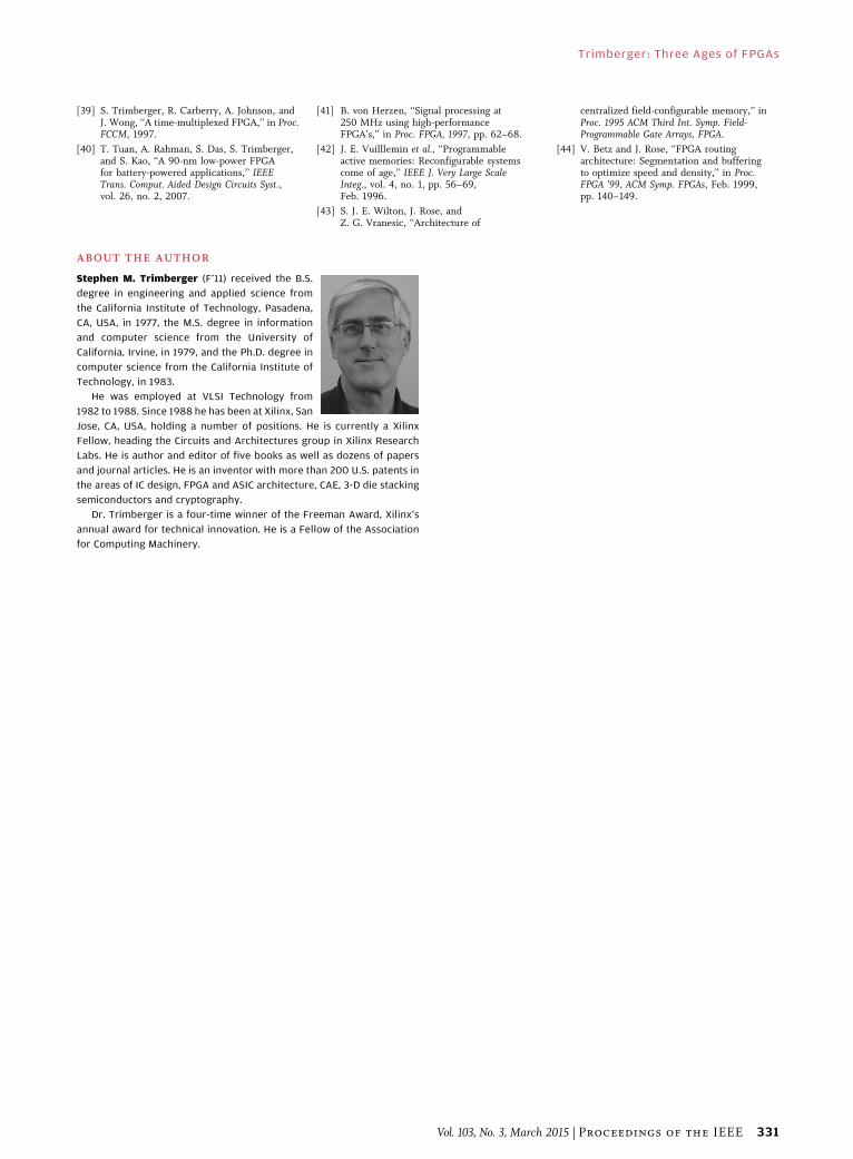
ABOUT T HE AUTHO R
Stephen M. Trimberger (F’11) received the B.S.
degree in engineering and applied science from
the California Institute of Technology, Pasadena,
CA, USA, in 1977, the M.S. degree in information
and computer science from the University of
California, Irvine, in 1979, and the Ph.D. degree in
computer science from the California Institute of
Technology, in 1983.
He was employed at VLSI Technology from
1982 to 1988. Since 1988 he has been at Xilinx, San
Jose, CA, USA, holding a number of positions. He is currently a Xilinx
Fellow, heading the Circuits and Architectures group in Xilinx Research
Labs. He is author and editor of five books as well as dozens of papers
and journal articles. He is an inventor with more than 200 U.S. patents in
the areas of IC design, FPGA and ASIC architecture, CAE, 3-D die stacking
semiconductors and cryptography.
Dr. Trimberger is a four-time winner of the Freeman Award, Xilinx’s
annual award for technical innovation. He is a Fellow of the Association
for Computing Machinery.
Trimberger: Three Ages of FPGAs
Vol. 103, No. 3, March 2015 | Proceedings of the IEEE 331