Embed Size (px)
Citation preview
Near Junction Thermal Transport and Embedded Cooling of High Power GaN Electronics
Carlton T. Creamer1*, Pane C. Chao1, Kenneth K. Chu1, Adonis Kassinos1, Geoffrey Campbell2, Henry Eppich2, A.Shooshtari3, S. Dessiatoun3, M. Ohadi3, Craig McGray4, Ray Kallaher4
1Advanced RF Microelectronics, Technology Solutions, BAE Systems, Nashua NH 2Science Research Laboratories, Somerville, MA
3University of Maryland, College Park, MD4Modern Microsystems, Silver Springs, MD
*e-mail: [email protected] *Phone: 603-885-1275
Keywords: GaN-on-Diamond, microchannel cooling, chip scale embedded cooling, high power density
AbstractGallium-Nitride (GaN) MMIC circuits have been
developed that achieve much greater RF power density compared to GaAs based predecessors. Even greater power densities are possible from these wideband gap devices. However, the requirement to maintain reliable junction temperatures limits both linear and areal power densities. Under the DARPA-sponsored NJTT and ICECool Applications programs, chip-scale thermal management solutions are being developed that combine GaN-on-Diamond with microchannel embedded cooling solutions that enable reliable MMIC operation at heat flux levels of >1kW/cm2 .
INTRODUCTION
Efforts to mature gallium nitride on silicon carbide (GaN-on-SiC) have been successful largely due to steady U.S. Government and industry investment for over a decade beginning around 2000 [1]. Although GaN-on-SiC devices now produce greater than 10x power density compared to the predominant predecessor GaAs [2], GaN has not yet been exploited to its full potential mostly owing to a limited ability to expel waste heat, and must therefore be operated at a derated electrical condition in order to maintain channel temperatures at or below levels required for 106 hours of reliable operation. With Near Junction Thermal Transport and Embedded Cooling of High Power GaN Electronics, thermal limitations are overcome through the use of embedded, chip-scale thermal management techniques that are the critical enablers to achieving increased power density, leading to a significant system performance advantage. Chip-scale thermal management combines the use of a passive diamond MMIC substrate that replaces the native SiC via a bonding method [3] with a high performance microchannel cooler that boasts volumetric heat capacity of greater than 10kW/cm3 [4].
MOTIVATION AND PERSPECTIVE
1) Higher RF power density provides flexibility to the system designer to conduct performance trades of range, cooling, SWaP, reliability, and payload capability/volume. For example, greater power per element will produce AESAs with increased effective range for electronic attack or radar. Alternatively, the array may be configured with fewer higher power elements in a “sparse array” in order to lower size and weight or cost. This in turn enables low volume payloads for deployment on small platforms.
TABLE ISYSTEM FLEXIBILITY ENABLED BY
CHIP-SCALE THERMAL MANAGEMENT
2) Reduced Cooling System Size and Power-Typically, a coolant pumping system can consume ~20% of the overall system’s available prime power. Modern, large phased array systems require liquid cooling to maintain chassis baseplate temperatures at small deltas above fluid inlet. Through the application of embedded cooling technology, the total thermal resistance to the semiconductor junction can be lowered, allowing for a relaxation in the baseplate
Distribution Statement "A" (Approved for Public Release, Distribution Unlimited)
GaN-on-SiC GaN-on-Diamond
High Reliability High Power per Element
Relaxed Baseplate Temp.
Very High Power
Performance • Same performance, higher reliability (MTTF)
•Higher power•Same reliability (MTTF)
•Equivalent reliability (MTTF) and performance •Operate at higher baseplate temperatures
•High power, short lifetime •Not thermally limited
System Impact
• Greater Mission Lifetime
• Greater range and capability
• Reduced element account
• Reduced cooling Swap
• Enables payloads on smaller platforms
• Very High power in small volumes
Channel Temp.
Baseplate Temp.
RF Power
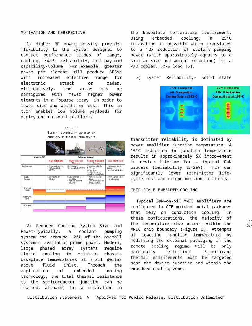
Figure 2-IR image of GaN-on-SiC (Left) and GaN-on-Diamond (Right) Transistors
Figure 4-Single Phase Micro-channel Cooler
temperature requirement. Using embedded cooling, a 25ºC relaxation is possible which translates to a >2X reduction of coolant pumping power (which approximately equates to a similar size and weight reduction) for a PAO cooled, 60kW load [5].
3) System Reliability- Solid state transmitter reliability is dominated by power amplifier junction temperature. A 10ºC reduction in junction temperature results in approximately 5X improvement in device lifetime for a typical GaN process (reliability EA~2eV). This can significantly lower transmitter life-cycle cost and extend mission lifetimes.
CHIP-SCALE EMBEDDED COOLING
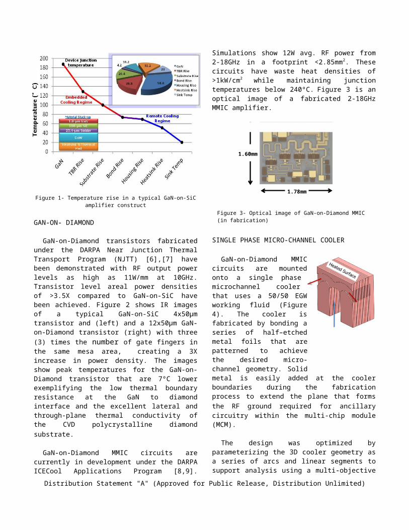
Typical GaN-on-SiC MMIC amplifiers are configured in CTE matched metal packages that rely on conduction cooling. In these configurations, the majority of the temperature rise occurs within the MMIC chip boundary (Figure 1). Attempts at lowering junction temperature by modifying the external packaging in the remote cooling regime will be only marginally effective. Significant thermal enhancements must be targeted near the device junction and within the embedded cooling zone.
Figure 1- Temperature rise in a typical GaN-on-SiC amplifier construct
GAN-ON- DIAMOND
GaN-on-Diamond transistors fabricated under the DARPA Near Junction Thermal Transport Program (NJTT) [6],[7] have been demonstrated with RF output power levels as high as 11W/mm at 10GHz. Transistor level areal power densities of >3.5X compared to GaN-on-SiC have been achieved. Figure 2 shows IR images of a typical GaN-on-SiC 4x50µm transistor and (left) and a 12x50µm GaN-on-Diamond transistor (right) with three (3) times the number
of gate fingers in the same mesa area, creating a 3X increase in power density. The images show peak temperatures for the GaN-on-Diamond transistor that are 7ºC lower exemplifying the low thermal boundary resistance at the GaN to diamond interface and the excellent lateral and through-plane thermal conductivity of the CVD polycrystalline diamond substrate.
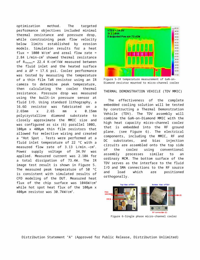
GaN-on-Diamond MMIC circuits are currently in development under the DARPA ICECool Applications Program [8,9]. Simulations show 12W avg. RF power from 2-18GHz in a footprint <2.85mm2. These circuits have waste heat densities of >1kW/cm2 while maintaining junction temperatures below 240ºC. Figure 3 is an optical image of a fabricated 2-18GHz MMIC amplifier.
SINGLE PHASE MICRO-CHANNEL COOLER
GaN-on-Diamond MMIC circuits are mounted onto a single phase microchannel cooler that uses a 50/50 EGW working fluid (Figure 4). The cooler is fabricated by bonding a series of half–etched metal foils that are patterned to achieve the desired micro-channel geometry. Solid metal is easily added at the cooler boundaries during the fabrication
Distribution Statement "A" (Approved for Public Release, Distribution Unlimited)
75ᵒC Baseplate,4W Dissipation,
Center Gate at 202ᵒC
75ᵒC Baseplate,12W Dissipation,
Center Gate at 195ᵒC
3X gate density in same mesa area
Photograph of GaN on SiC 4 x 50µm transistor (200µm)
Photograph of GaN on diamond 12 x 50µm transistor (600µm)
Figure 3- Optical image of GaN-on-Diamond MMIC (in fabrication)
1.78mm
1.60mm
process to extend the plane that forms the RF ground required for ancillary circuitry within the multi-chip module (MCM).
The design was optimized by parameterizing the 3D cooler geometry as a series of arcs and linear segments to support analysis using a multi-objective optimization method. The targeted performance objectives included minimal thermal resistance and pressure drop, while constraining peak flow velocity below limits established by erosion models. Simulation results for a heat flux = 1000 W/cm2 and areal flow rate = 2.84 L/min-cm2 showed thermal resistance of RThermal= 22.4 K-cm2/kW measured between the fluid inlet and the heated surface and a ∆P = 17.6 psi. Cooler performance was tested by measuring the temperature of a thin film TaN resistor using an IR camera to determine peak temperature, then calculating the cooler thermal resistance. Pressure drop was measured using the built-in pressure sensor at fluid I/O. Using standard lithography, a 16.6Ω resistor was fabricated on a 2.65mm x 2.65 mm x 0.15mm polycrystalline diamond substrate to closely approximate the MMIC size and was configured as six (6) parallel 100Ω, 100µm x 400µm thin film resistors that allowed for selective wiring and created a “Hot Spot”. Tests were performed at a fluid inlet temperature of 22 ºC with a measured flow rate of 3.13 L/min.-cm2. Power supply voltage of 34.9V was applied. Measured current was 2.10A for a total dissipation of 73.4W. The IR image test result is shown in Figure 5. The measured peak temperature of 50 ºC is consistent with simulated results of CFD modeling of the DUT. Measured heat flux of the chip surface was 1046W/cm2 while hot spot heat flux of the 100µm x 400µm resistor was 30.7kW/cm2.
Figure 5-IR temperature measurement of GaN-on-Diamond resistor mounted to micro-channel cooler
THERMAL DEMONSTRATION VEHICLE (TDV MMIC)
The effectiveness of the complete embedded cooling solution will be tested by constructing a Thermal Demonstration Vehicle (TDV). The TDV assembly will combine the GaN-on-Diamond MMIC with the high heat capacity micro-channel cooler that is embedded into the RF
ground plane. (see Figure 6). The electrical components, including the MMIC, RF and DC substrates, and bias injection circuits are assembled onto the top side of the cooler using conventional assembly processes similar to an ordinary MCM. The bottom surface of the TDV serves as the interface to the fluid I/O and SMA connections to the RF source and load which are positioned orthogonally.
Bottom View of TDV Top View of TDV
Cooler InletCooler Outlet (2)
RF connection (2)
MMIC
Bias substrates
Figure 6-Single phase micro-channel cooler
CONCLUSIONSSystem designers will always push to add functionality or
performance enhancements that will increase electronics density within fixed payload volumes. The resulting increase in waste heat density will tax conventional thermal management approaches beyond current capability to handle the projected extreme heat loads. Advancements in embedded thermal management like diamond substrate materials and microcooler packaging are important enabling technologies that will allow systems designers to realize higher performance transmitters in smaller available envelopes. ACKNOWLEDGEMENTS
This research was supported by the Defense Advanced Research Projects Agency (DARPA) under the NJTT and ICECool Applications Programs. The authors would like to acknowledge the contributions and thank Dr. Avi Bar-Cohen, Dr. Joseph Maurer, Dr. Kaiser Matin, Dr. Abirami Sivananthan, Dr. Avinash Kane, and Dr. Jonathan Felbinger. The authors would also like to recognize Mr. John Blevins and Mr. David Via from Air Force Research Laboratory for their numerous contributions and support in characterization and measurement of GaN-on-Diamond transistors. The views, opinions, and/or findings contained in this article/presentation are those of the author/presenter and should not be interpreted as representing the official views or policies, either expressed or implied, of the Defense Advanced Research Projects Agency, Air Force or the Department of Defense.
REFERENCES[1] Mark Rosker, Christopher Bozada, Harry Dietrich, Alfred Hung, Dave
Via, Steve Binari, Ed Viveiros, Eliot Cohen and Justin Hodiak; “The DARPA Wide Band Gap Semiconductors for RF Applications (WBGS-RF) Program: Phase II Results”; CS MANTECH Conference, May 18th-21st, 2009, Tampa, Florida, USA.
Distribution Statement "A" (Approved for Public Release, Distribution Unlimited)
VTDV =34.9VI=2.104ADissipated Power=73.43W
[2] P. Parikh, Y. Wu, N. Zhang, P. Chavarkar, M. Moore, U. Mishra,W. Pribble, J. Palmour, L. Kehias, T. Jenkins “Power GaN-based Microwave Devices for Wireless Communications” 2001 GaAs MANTECH, Inc.
[3] P.C. Chao, Kanin Chu and Carlton Creamer “A New High Power GaN-on-Diamond HEMT with Low-Temperature Bonded Substrate Technology” CS MANTECH Conference, May 13th - 16th, 2013, New Orleans, Louisiana, USA.
[4] Geoffrey Campbell, Henry Eppich, Keith Lang, Carlton Creamer, Thomas Yurovchak, Kanin Chu, Adonis Kassinos, Michael Ohadi, Amir Shooshtari, Serguei Dessiatoun, “Advanced Cooling Designs for GaN on Diamond MMICs”; Proceedings of the ASME 2015 International Technical Conference and Exhibition on Packaging and Integration of Electronic and Photonic Microsystems and ASME 2015 12th International Conference on Nanochannels, Microchannels, and Minichannels InterPACKICNMM2015 July 6-9, 2015, San Francisco, California, USA.
[5] Dan Kinney, Andy Johnston “Two-phase cooling meets the challenges of modern radar applications”; Embedded Military Systems.
[6] Pane-Chane Chao, Kenneth Chu, Carlton Creamer, Jose Diaz, Tom Yurovchak, Michael Shur, Ray Kallaher , Craig McGray, Glen David Via, John D. Blevins “Low-Temperature Bonded GaN-on-Diamond HEMTs With 11W/mm Output Power at 10GHz” IEEE Transactions on Electron Devices Vol 62 No. 11, November 2015.
[7] D.C. Dumka, T.M. Chou, J.L. Jimenez, D.M. Fanning, D. Francis, F. Failia, F. Ejeckam, M. Bernardoni, J.W. Pomeroy, and M. Kuball, “Electrical and Thermal Performance of AlGaN/GaN HEMTs on Diamond Substrate for RF Applications” Compound Semiconductor Integrated Circuit Symposium (CSICS) 2013.
[8] Avram Bar-Cohen, Joseph J. Maurer, Jonathan G. Felbinger “DARPA’s Intra/Interchip Enhanced Cooling (ICECool) Program” CS MANTECH Conference, May 13th - 16th, 2013, New Orleans, Louisiana, USA.
[9] C.T. Creamer, K.K. Chu, P.C. Chao, B. Schmanski, T. Yurovchak, S. Sweetland, Geoff Campbell and Henry Craig McGray; “Microchannel Cooled, High Power GaN on Diamond MMIC”, 2014 Lester Eastman Conference.
ACRONYMS
NJTT: Near Junction Thermal TransportICECool: Intra-Chip Enhanced CoolingMMIC: Microwave Monolithic Integrated CircuitSWaP: Size, Weight and PowerAESA: Active Electronically Steered ArrayPAO: PolyalphaolefinCTE: Coefficient of Thermal ExpansionEGW: Ethylene Glycol and water CVD: Chemical Vapor DepositionCFD: Computational Fluid Dynamic
Distribution Statement "A" (Approved for Public Release, Distribution Unlimited)


![Paper Formating Guidelines - CS MANTECHcsmantech.org/OldSite/Digests/2016/[0711-000059][2016 CS... · Web viewThis difficulty arises from the high temperatures to achieve p-type doping](https://img.pdfslide.us/doc/110x75/5b04cfc97f8b9a3c378e2fd6/paper-formating-guidelines-cs-0711-0000592016-csweb-viewthis-difficulty-arises.jpg)