Embed Size (px)
Citation preview

Characterization and Modeling of Sub-Harmonic Oscillations in GaAs and GaN FET Technologies
Mike Salib and Imad Ahmad
Northrop Grumman Corporation, Aviation Boulevard, Linthicum Heights, MD 21090 USAe-mail: [email protected] Phone: 410-765-7513, e-mail: [email protected] Phone: 410-765-4238
Keywords: Power Amplifiers, HPA, Parametric Oscillations, Sub-Harmonic Oscillations, GaAs PHEMT, GaN HEMT STAN TOOL , Focus Load Pull, f/2 oscillation.
AbstractThis paper presents a method of characterizing a FET
using a commercially available Focus Load Pull Tuner System for input impedances to the FET resulting in Fin/2 oscillations when the FET is under large signal drive at frequency, Fin. Such oscillations are referred to as parametric oscillations. These oscillations are detrimental to the systems that use such power amplifiers. The characterization gives an understanding of impedances that may cause the FET to oscillate if they are present at the input. FETs from the GaAs and GaN technologies were characterized and modeled.
INTRODUCTION
In compound semiconductor FETs and HBTs, parametric oscillations may occur under large signal drive close to 1 dB gain compression of the FET. These oscillations occur only under large signal drive. The parametric oscillation often takes place at the sub-harmonic frequency Fin/n where Fin is the drive frequency and n is an integer value that could be as high as 30 [1]. This paper will focus on oscillations when n equals 2. Such parametric oscillations must be minimized because they are detrimental to systems like Radar that use these types of power amplifiers.
This paper will cover four topics. First we will show a method, using a reconfigurable multi-probe Load-Pull system, to characterize the transistors in order to stabilize the FET or the HBT without losing valuable gain. Then we will discuss modeling that shows good agreement with the measured input impedances that make the transistor oscillate at Fin/2. We will also show the characterizations that were done on GaAs pHEMTs and GaN HEMTs and the difference in the 2 technologies in the area of the parametric oscillations. Finally, we will present an insight into the phenomena of parametric oscillations.
Characterization of the FET for Fin/2 oscillations
Figure 1 shows the setup used to characterize the FET for the Fin/2 oscillations. It is a Load-Pull system with an input tuner that has 2 slugs that can present calculated impedances
at 2 independent frequencies. In this case it was configured for fundamental and sub-harmonic frequencies. The tuner was used to map the impedance at the sub-harmonic frequency and record the output spectrum at the sub-harmonic and the fundamental frequencies. The input tuner is used to conjugate match the input of the transistor to drive it with the available power source at the fundamental frequency Fin. As the impedance of the tuner is mapped at the sub-harmonic frequency the impedance at the fundamental stays fixed.
Fig.1 Focus Load Pull System used for the FET Characterization for Sub-Harmonic Oscillation Source Impedances
A 0.25um pHEMT FET from Qorvo was characterized at 10 GHz and the results are shown in figure 2. The input power level to the FET was set for 2 dB compression at F in. The data shown in the figure is the strength of the F in/2 oscillation corresponding to the various impedances presented to the input of the FET and plotted on the smith chart. The strength of the Fin/2 signal is color coded where red is the highest and blue is the lowest. The area of the smith chart where the FET had Fin/2 oscillations is circled. The FET equivalent circuit is a series resistance and inductance. The strength of the sub-harmonic oscillation increases as the series resistance decreases; if the input of the FET has a negative resistance in the state of oscillation, adding a positive series resistance would stabilize it. This point will be further explained in section four. The

imaginary part shows that oscillation occurs only when the input capacitance of the FET is resonated out at the sub-harmonic frequency.
Fig.2 Area of the Smith Chart at which the source impedance has caused Sub-Harmonic Oscillation. The color scale demonstrates the strength of the Sub-Harmonic oscillation signal for the different source impedances on the smith chart measured on the Spectrum Analyzer. The magnitude is about -5.5dBc.
Modeling of the Fin/2 oscillation using commercially available FET models and simulation tools
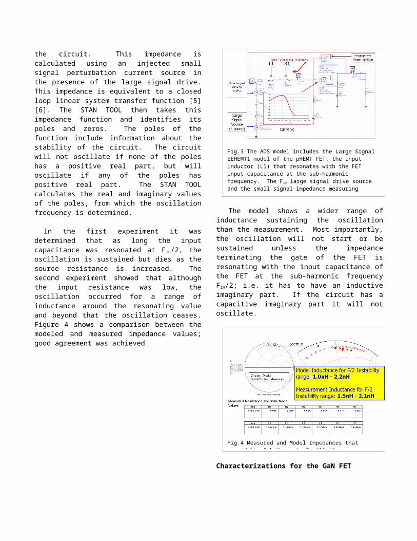
The modeling was done using the Harmonic Balance test bench on ADS. The pHEMT large signal model used was the EEHEMT1. The ADS setup is shown in Figure 3. The FET was resonated with an inductor at F in/2 and the source resistance was varied from 0 to 50 Ohms. Additionally, the source resistance was fixed at 0.5 Ohm and the resonating inductance was varied by +/- 30% around the resonating value. In each case the stability was determined by the STAN TOOL software [4].
The STAN TOOL is a commercially available software that uses the small signal calculated impedance at the gate of the FET to identify the stability of the circuit. This impedance is calculated using an injected small signal perturbation current source in the presence of the large signal drive. This impedance is equivalent to a closed loop linear system transfer function [5] [6]. The STAN TOOL then takes this impedance function and identifies its poles and zeros. The poles of the function include information about the stability of the circuit. The circuit will not oscillate if none of the poles has a positive real part, but will oscillate if any of the poles has positive real part. The STAN TOOL calculates the real and imaginary values of the poles, from which the oscillation frequency is determined.
In the first experiment it was determined that as long the input capacitance was resonated at Fin/2, the oscillation is sustained but dies as the source resistance is increased. The second experiment showed that although the input resistance
was low, the oscillation occurred for a range of inductance around the resonating value and beyond that the oscillation ceases. Figure 4 shows a comparison between the modeled and measured impedance values; good agreement was achieved.
Fig.3 The ADS model includes the Large Signal EEHEMT1 model of the pHEMT FET, the input inductor (L1) that resonates with the FET input capacitance at the sub-harmonic frequency. The Fin large signal drive source and the small signal impedance measuring source are also shown. The Fin is also often referred to as the pump frequency (f_pump)
The model shows a wider range of inductance sustaining the oscillation than the measurement. Most importantly, the oscillation will not start or be sustained unless the impedance terminating the gate of the FET is resonating with the input capacitance of the FET at the sub-harmonic frequency Fin/2; i.e. it has to have an inductive imaginary part. If the circuit has a capacitive imaginary part it will not oscillate.
Fig.4 Measured and Model Impedances that caused the Sub-Harmonic Oscillation
Characterizations for the GaN FET
Next, a GaN HEMT was characterized, modeled and compared to a GaAs pHEMT FET. The input capacitance
was extracted versus gate bias from the measured S-parameters of the FET as a function of gate bias. The EEHEMT1 Large signal model for the same device was also used to extract the input capacitance versus gate voltage. Good agreement was found between the measured and the model input capacitance. This measurement is important because the prediction of the oscillation is dependent on how accurate the large signal model is with respect to the capacitance non-linearity. Figure 5 shows the GaN FET and GaAs FET input capacitance on the same plot. It is clear that the GaAs pHEMT is more non-linear than the GaN FET because the capacitance change of the GaAs pHEMT is almost 4:1 over a 1 V range of gate voltage where the GaN is 2:1 over a 5 V. The ADS model was used to calculate the value for the series resistance that stops the oscillation at the sub-harmonic. The GaN HEMT stabilized at 3 Ohm.mm where the GaAs pHEMT stabilized at 9 Ohm.mm. Higher non-linearity in the Cgs capacitance of the FET requires a higher value of resistance to stabilize it. Figure 6 shows the Fin/2 characterization that was done on the Qorvo 0.15um GaN HEMT.
Fig5. Input Capacitance (Cin(pF)) v.s. Gate Voltage for the GaAs pHEMT and the GaN HEMT
Fig.6 Area of the Smith Chart at which the source impedance causes Sub-Harmonic Oscillation and its corresponding frequency spectrum for the Qorvo 0.15m GaN HEMT.
Why does the oscillation occur at half of the fundamental frequency?
The mechanism of the sub-harmonic oscillation may be understood by the aid of a reverse biased varactor diode whose capacitance can be varied using a sinusoidal time periodic function. The time domain setup in ADS is shown in Figure 7. The capacitance of the varactor is also shown in the figure. The varactor was biased at -0.9 V. The peak of the pumping signal is 1 V. The sinusoidal signal is set to 3 GHz. The pump signal Vs changes the diode’s capacitance with time in the same manner as a capacitor whose plates are being pulled apart periodically with time. An inductor in the loop resonates with average capacitance of one cycle at 1.5 GHz. Energy is exerted to pull the capacitor plates apart. This energy is from the sinusoidal time periodic signal set in this case to frequency 3 GHz. An inductor is placed across the capacitor to resonate with it at the sub-harmonic frequency Fin/2. As a result of this capacitance change and the resonance, voltage across the capacitor builds up from one cycle to the next at the Fin/2 frequency.

Fig. 7 Understanding the Sub-Harmonic oscillation in the FET using the swept Reverse Biased Varactor Diode
The above mechanism is shown is figure 8. At point A, the large signal voltage of fundamental frequency F in across the diode is a sinusoidal signal in time. This signal voltage changes the diode capacitance from a maximum to a minimum value. At point A and C the capacitance of the diode is at the minimum value and at point B the capacitance is the maximum value. The relationship Q=CV exists where Q is the diode capacitor charge, V is the voltage across it and C is the capacitance. The charge Q on the diode capacitor is fixed and therefore as the capacitance is lowered the voltage increases. At the negative cycles of the signal F in, the capacitance is pulled to a low value and accordingly the positive and the negative cycles of the Fin/2 signal increase in magnitude. These are points A and C. It takes 2 cycles from Fin to build one cycle of the Fin/2 signal.
Fig. 8 Steps of the Sub-Harmonic signal growth from cycle to cycle of the drive signal
From cycle to cycle the process continues and the Fin/2 signal continues to grow. It is the phase relationship between
the Fin and the Fin/2 that makes it the dominant mode of oscillation and supported by the resonance that confines the growth to the Fin/2. The growth continues until it is limited by the resistance in the loop. The voltage increase at F in/2 is shown in figure 9. Reference [7] shows the same principle explained here but with a motor pulling apart the 2 plates of a capacitor is in time varying sinusoidal signal. The oscillation frequency at the sub harmonic builds up from cycle to cycle. The resonating inductor is also in the circuit.
Fig. 9 The Voltage at the sub-harmonic frequency (1.5GHz) continues to grow until it is stabilized by the loop resistance. The drive frequency is 3GHz.
Figure 10 shows the fundamental and the sub-harmonic signal as a function of drive. As the drive level is increased the power at Fin increases but the power at F in/2 does not. At Pin = 3.5dB the Fin/2 power increases significantly and then stays fairly flat until Pin = 7dB. Between Pin = 3 and 7 dB the capacitance range of the FET is fully swept by the drive signal. Above Pin = 7dB, the gate source junction becomes forward biased and the FET input resistance increases and therefore the oscillation stops.
Fig.10 Swept Pout for the Fundamental (Fin) and Fin/2 versus Pin

CONCLUSIONS
The Focus load pull system was used to characterize a GaAs pHEMT and the GaN HEMT and data was presented for the f/2 oscillation that results when the FET is driven into compression and the right conditions for oscillation exist. The results show that an oscillation starts if the FET is presented with a terminating imaginary impedance that is close to resonance at the f/2 and a series resistance that is below a certain value. The value of the stabilizing resistance is directly proportional to the non-linearity of Cgs. The modeling for the GaAs pHEMT which has much more non-linear capacitance than the GaN HEMT, showed that the stabilizing resistance is 3 times higher. The strength of the
oscillation is also dependent on the non-linearity of the Cgs capacitance. Measurements were also supported by models and an intuitive explanation of how the oscillation starts.
REFERENCES
[1] Sokal presented Parasitic Oscillations in Solid State PA IEEE Electro/80, Boston, MA
[2] Focus Microwaves Inc. [3] ICCAP by Keysight Technologies. [4] STAN TOOL from AMCAD Engineering[5] J. Jugo, J. Portilla, A. Anakabe, A. Suarez and J. Collantes Elec. Letters
Feb 2001 Vol 37 No4 [6] A. Anakabe, J.M. Collantes, J. Portilla, J. Jugo, IEEE MTT-S Digest,
pp. 2181-2184, 2002[7] Theory and Application of Parametric Excitation. Dr. Robert Melville
IMS 2009 Workshop
![Paper Formating Guidelinescsmantech.org/OldSite/Digests/2016/[0711-000040][2016 CS... · Web viewbake is used to fully cure the resin after printing. Examples of compound semiconductor](https://img.pdfslide.us/doc/110x75/5aab3d0a7f8b9a2b4c8bc28e/paper-formating-0711-0000402016-csweb-viewbake-is-used-to-fully-cure-the-resin.jpg)
![J.K - CS MANTECHcsmantech.org/OldSite/Digests/2016/[0711-000060][2016 CS... · Web viewSchematic of 2-metal layer HBT Interconnect using low-K BCB ILD and overcoat and SiN dielectrics,](https://img.pdfslide.us/doc/110x75/5e51caeb1511a62a86377828/jk-cs-0711-0000602016-cs-web-view-schematic-of-2-metal-layer-hbt-interconnect.jpg)

![TITLE - CS MANTECHcsmantech.org/OldSite/Digests/2016/[0711-000062][2016 CS... · Web viewinto a variety of military radar, electronic warfare and communication systems as well as](https://img.pdfslide.us/doc/110x75/5ae315197f8b9a097a8db87d/title-cs-0711-0000622016-csweb-viewinto-a-variety-of-military-radar-electronic.jpg)