Embed Size (px)
Citation preview
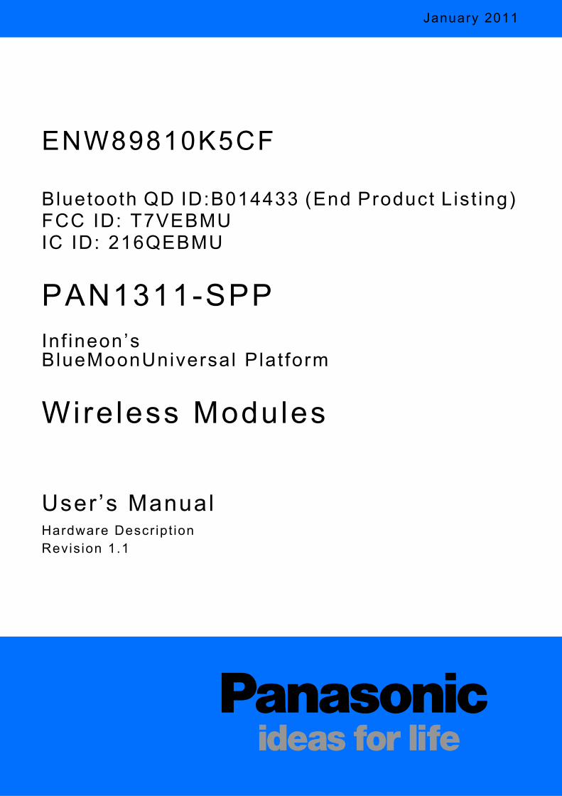
January 2011
User ’s ManualHardware Descr ipt ionRevis ion 1.1
ENW89810K5CF
Bluetooth QD ID:B014433 (End Product List ing)FCC ID: T7VEBMUIC ID: 216QEBMU
PAN1311-SPPInf ineon’s BlueMoonUniversal Plat form
Wireless Modules

November 2011
User ’s ManualHardware Descr ipt ionRevis ion 3.3
ENW89811xxxF
Bluetooth QD ID:B014433 (End Product List ing)FCC ID: T7VEBMUIC ID: 216QEBMU
PAN1321-SPPIntel ’s BlueMoonUniversal Plat form
Wireless Modules
Edition 2011-11-16Published by Panasonic Electronic Devices Europe GmbH Zeppelinstrasse 19 D-21337 Lüneburg, Germany© 2011 Panasonic Electronic Devices Europe GmbH All Rights Reserved.
Legal DisclaimerThe information given in this document shall in no event be regarded as a guarantee of conditions or characteristics. With respect to any examples or hints given herein, any typical values stated herein and/or any information regarding the application of the device, Panasonic Electronic Devices Europe GmbH hereby disclaims any and all warranties and liabilities of any kind, including without limitation, warranties of non-infringement of intellectual property rights of any third party.
InformationFor further information on technology, delivery terms and conditions and prices please contact your nearest Panasonic Office in Germany or one of our Distributor or write an e-mail to [email protected].
WarningsDue to technical requirements components may contain dangerous substances. For information on the types in question please contact your nearest Panasonic Office.Panasonic Electronic Devices may only be used in life-support devices or systems with the express written approval of Panasonic Devices, if a failure of such components can reasonably be expected to cause the failure of that life-support device or system, or to affect the safety or effectiveness of that device or system. Life support devices or systems are intended to be implanted in the human body, or to support and/or maintain and sustain and/or protect human life. If they fail, it is reasonable to assume that the health of the user or other persons may be endangered.
Initial versionDue to better range with another ceramic antenna, we have updated module height from 1.8mm to 2.8mm. Changes made in “Production Package” on Page 29If you need smaller height, let us discuss your individual case.Releasing this document and correct the ordering code to ENW89811xxxF, which is the 85°C versionAdd the Chapter 9, Modified Figure 6 “Package Marking” on Page 29 and Figure 8 “Top View and Bottom View” on Page 30Fixed all pins for the product life time in Chapter 1.4. Added Table 2 “Firmware Releases as of 2011-11-16” on Page 13 and updated the Chapter 12.Updated the following:Chapter 12 Added the following: Chapter 4.3 “Apple® iPhone Support” on Page 16, Chapter 5 “Ordering Information” on Page 17,
User’s Manual 3 Revision 3.3, 2011-11-16Hardware Description
PAN1321-SPPENW89811xxxF
Trademark Information:BlueMoon® is a trademark of Intel Mobile Communications GmbH.IPhone®, iPad®, iPad® and Apple® are trademarks of Apple Inc.
ENW89811xxxF - Intel’s BlueMoonTM Universal Platform Revision History: 2011-11-16, Revision 3.3Previous Version: 3.2Page Subjects (major changes since last revision)Rev1.0Rev2.0
Rev3.0Rev3.1
Rev3.2
Rev3.3

PAN1321-SPPENW89811xxxFTable of Contents
Table of Contents
Table of Contents . . . . . . . . . . . . . . . . . . . . . . . . . . . . . . . . . . . . . . . . . . . . . . . . . . . . . . . . . . . . . . . . 4
List of Figures . . . . . . . . . . . . . . . . . . . . . . . . . . . . . . . . . . . . . . . . . . . . . . . . . . . . . . . . . . . . . . . . . . . 6
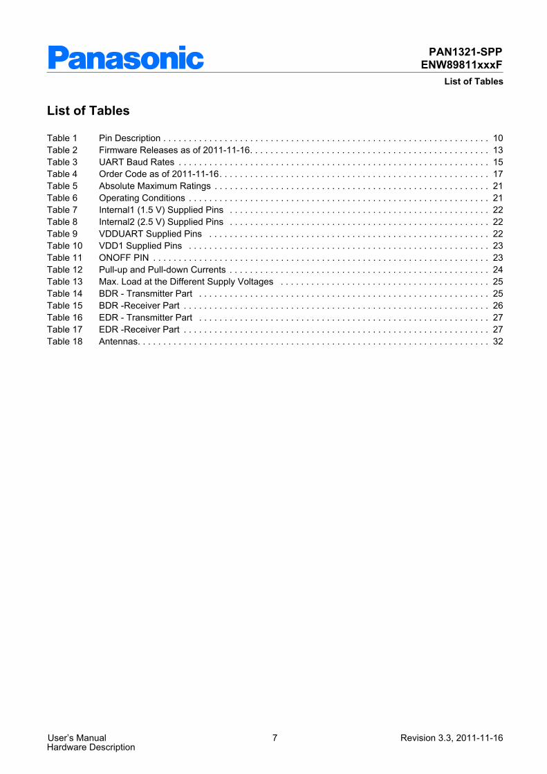
List of Tables . . . . . . . . . . . . . . . . . . . . . . . . . . . . . . . . . . . . . . . . . . . . . . . . . . . . . . . . . . . . . . . . . . . . 7
1 General Device Overview . . . . . . . . . . . . . . . . . . . . . . . . . . . . . . . . . . . . . . . . . . . . . . . . . . . . . . . . . . 81.1 Features . . . . . . . . . . . . . . . . . . . . . . . . . . . . . . . . . . . . . . . . . . . . . . . . . . . . . . . . . . . . . . . . . . . . . . . . 81.2 Block Diagram . . . . . . . . . . . . . . . . . . . . . . . . . . . . . . . . . . . . . . . . . . . . . . . . . . . . . . . . . . . . . . . . . . . 91.3 Pin Configuration LGA . . . . . . . . . . . . . . . . . . . . . . . . . . . . . . . . . . . . . . . . . . . . . . . . . . . . . . . . . . . . . 91.4 Pin Description . . . . . . . . . . . . . . . . . . . . . . . . . . . . . . . . . . . . . . . . . . . . . . . . . . . . . . . . . . . . . . . . . . 101.5 System Integration . . . . . . . . . . . . . . . . . . . . . . . . . . . . . . . . . . . . . . . . . . . . . . . . . . . . . . . . . . . . . . . 121.6 FW version . . . . . . . . . . . . . . . . . . . . . . . . . . . . . . . . . . . . . . . . . . . . . . . . . . . . . . . . . . . . . . . . . . . . . 13
2 Basic Operating Information . . . . . . . . . . . . . . . . . . . . . . . . . . . . . . . . . . . . . . . . . . . . . . . . . . . . . . 142.1 Power Supply . . . . . . . . . . . . . . . . . . . . . . . . . . . . . . . . . . . . . . . . . . . . . . . . . . . . . . . . . . . . . . . . . . . 142.2 Clocking . . . . . . . . . . . . . . . . . . . . . . . . . . . . . . . . . . . . . . . . . . . . . . . . . . . . . . . . . . . . . . . . . . . . . . . 14
3 Interfaces . . . . . . . . . . . . . . . . . . . . . . . . . . . . . . . . . . . . . . . . . . . . . . . . . . . . . . . . . . . . . . . . . . . . . . 153.1 UART Interface . . . . . . . . . . . . . . . . . . . . . . . . . . . . . . . . . . . . . . . . . . . . . . . . . . . . . . . . . . . . . . . . . . 153.1.1 UART . . . . . . . . . . . . . . . . . . . . . . . . . . . . . . . . . . . . . . . . . . . . . . . . . . . . . . . . . . . . . . . . . . . . . . . . 153.1.1.1 Baud Rates . . . . . . . . . . . . . . . . . . . . . . . . . . . . . . . . . . . . . . . . . . . . . . . . . . . . . . . . . . . . . . . . . 15
4 General Device Capabilities . . . . . . . . . . . . . . . . . . . . . . . . . . . . . . . . . . . . . . . . . . . . . . . . . . . . . . . 164.1 HCI+ . . . . . . . . . . . . . . . . . . . . . . . . . . . . . . . . . . . . . . . . . . . . . . . . . . . . . . . . . . . . . . . . . . . . . . . . . . 164.2 Firmware ROM Patching . . . . . . . . . . . . . . . . . . . . . . . . . . . . . . . . . . . . . . . . . . . . . . . . . . . . . . . . . . 164.2.1 Patch Support . . . . . . . . . . . . . . . . . . . . . . . . . . . . . . . . . . . . . . . . . . . . . . . . . . . . . . . . . . . . . . . . . 164.3 Apple® iPhone Support . . . . . . . . . . . . . . . . . . . . . . . . . . . . . . . . . . . . . . . . . . . . . . . . . . . . . . . . . . . 164.3.1 Apple® Authentication Chip . . . . . . . . . . . . . . . . . . . . . . . . . . . . . . . . . . . . . . . . . . . . . . . . . . . . . . . 17
5 Ordering Information . . . . . . . . . . . . . . . . . . . . . . . . . . . . . . . . . . . . . . . . . . . . . . . . . . . . . . . . . . . . 17
6 Bluetooth Capabilities . . . . . . . . . . . . . . . . . . . . . . . . . . . . . . . . . . . . . . . . . . . . . . . . . . . . . . . . . . . 186.1 Supported Features . . . . . . . . . . . . . . . . . . . . . . . . . . . . . . . . . . . . . . . . . . . . . . . . . . . . . . . . . . . . . . 186.2 PAN1321-SPP Specifics and Extensions . . . . . . . . . . . . . . . . . . . . . . . . . . . . . . . . . . . . . . . . . . . . . . 196.2.1 During Connection . . . . . . . . . . . . . . . . . . . . . . . . . . . . . . . . . . . . . . . . . . . . . . . . . . . . . . . . . . . . . . 196.2.1.1 Role Switch . . . . . . . . . . . . . . . . . . . . . . . . . . . . . . . . . . . . . . . . . . . . . . . . . . . . . . . . . . . . . . . . . 196.2.1.2 Dynamic Polling Strategy . . . . . . . . . . . . . . . . . . . . . . . . . . . . . . . . . . . . . . . . . . . . . . . . . . . . . . . 196.2.1.3 Adaptive Frequency Hopping (AFH) . . . . . . . . . . . . . . . . . . . . . . . . . . . . . . . . . . . . . . . . . . . . . . 196.2.1.4 Channel Quality Driven Data Rate Change (CQDDR) . . . . . . . . . . . . . . . . . . . . . . . . . . . . . . . . 196.2.2 RSSI and Output Power Control . . . . . . . . . . . . . . . . . . . . . . . . . . . . . . . . . . . . . . . . . . . . . . . . . . . 206.2.2.1 Received Signal Strength Indication (RSSI) . . . . . . . . . . . . . . . . . . . . . . . . . . . . . . . . . . . . . . . . 206.2.2.2 Output Power Control . . . . . . . . . . . . . . . . . . . . . . . . . . . . . . . . . . . . . . . . . . . . . . . . . . . . . . . . . 206.2.2.3 Ultra Low Transmit Power . . . . . . . . . . . . . . . . . . . . . . . . . . . . . . . . . . . . . . . . . . . . . . . . . . . . . . 20
7 Electrical Characteristics . . . . . . . . . . . . . . . . . . . . . . . . . . . . . . . . . . . . . . . . . . . . . . . . . . . . . . . . . 217.1 Absolute Maximum Ratings . . . . . . . . . . . . . . . . . . . . . . . . . . . . . . . . . . . . . . . . . . . . . . . . . . . . . . . . 217.2 Operating Conditions . . . . . . . . . . . . . . . . . . . . . . . . . . . . . . . . . . . . . . . . . . . . . . . . . . . . . . . . . . . . . 217.3 DC Characteristics . . . . . . . . . . . . . . . . . . . . . . . . . . . . . . . . . . . . . . . . . . . . . . . . . . . . . . . . . . . . . . . 227.3.1 Pad Driver and Input Stages . . . . . . . . . . . . . . . . . . . . . . . . . . . . . . . . . . . . . . . . . . . . . . . . . . . . . . 227.3.2 Pull-ups and Pull-downs . . . . . . . . . . . . . . . . . . . . . . . . . . . . . . . . . . . . . . . . . . . . . . . . . . . . . . . . . 247.3.3 Protection Circuits . . . . . . . . . . . . . . . . . . . . . . . . . . . . . . . . . . . . . . . . . . . . . . . . . . . . . . . . . . . . . . 247.3.4 System Power Consumption . . . . . . . . . . . . . . . . . . . . . . . . . . . . . . . . . . . . . . . . . . . . . . . . . . . . . . 257.4 AC Characteristics . . . . . . . . . . . . . . . . . . . . . . . . . . . . . . . . . . . . . . . . . . . . . . . . . . . . . . . . . . . . . . . 25
User’s Manual 4 Revision 3.3, 2011-11-16Hardware Description
PAN1321-SPPENW89811xxxFTable of Contents
7.5 RF Part . . . . . . . . . . . . . . . . . . . . . . . . . . . . . . . . . . . . . . . . . . . . . . . . . . . . . . . . . . . . . . . . . . . . . . . . 257.5.1 Characteristics RF Part . . . . . . . . . . . . . . . . . . . . . . . . . . . . . . . . . . . . . . . . . . . . . . . . . . . . . . . . . . 257.5.1.1 Bluetooth Related Specifications . . . . . . . . . . . . . . . . . . . . . . . . . . . . . . . . . . . . . . . . . . . . . . . . . 25
8 Package Information . . . . . . . . . . . . . . . . . . . . . . . . . . . . . . . . . . . . . . . . . . . . . . . . . . . . . . . . . . . . 298.1 Package Marking . . . . . . . . . . . . . . . . . . . . . . . . . . . . . . . . . . . . . . . . . . . . . . . . . . . . . . . . . . . . . . . . 298.2 Production Package . . . . . . . . . . . . . . . . . . . . . . . . . . . . . . . . . . . . . . . . . . . . . . . . . . . . . . . . . . . . . . 298.2.1 Pin Mark . . . . . . . . . . . . . . . . . . . . . . . . . . . . . . . . . . . . . . . . . . . . . . . . . . . . . . . . . . . . . . . . . . . . . . 30
9 Important Application Information . . . . . . . . . . . . . . . . . . . . . . . . . . . . . . . . . . . . . . . . . . . . . . . . . 319.1 Reference Design . . . . . . . . . . . . . . . . . . . . . . . . . . . . . . . . . . . . . . . . . . . . . . . . . . . . . . . . . . . . . . . . 319.2 FCC Class B Digital Devices Regulatory Notice . . . . . . . . . . . . . . . . . . . . . . . . . . . . . . . . . . . . . . . . . 329.3 FCC Wireless Notice . . . . . . . . . . . . . . . . . . . . . . . . . . . . . . . . . . . . . . . . . . . . . . . . . . . . . . . . . . . . . 329.4 FCC Interference Statement . . . . . . . . . . . . . . . . . . . . . . . . . . . . . . . . . . . . . . . . . . . . . . . . . . . . . . . . 339.5 FCC Identifier . . . . . . . . . . . . . . . . . . . . . . . . . . . . . . . . . . . . . . . . . . . . . . . . . . . . . . . . . . . . . . . . . . . 339.6 European R&TTE Declaration of Conformity . . . . . . . . . . . . . . . . . . . . . . . . . . . . . . . . . . . . . . . . . . . 339.7 Bluetooth Qualified Design ID . . . . . . . . . . . . . . . . . . . . . . . . . . . . . . . . . . . . . . . . . . . . . . . . . . . . . . . 359.8 Industry Canada Certification . . . . . . . . . . . . . . . . . . . . . . . . . . . . . . . . . . . . . . . . . . . . . . . . . . . . . . . 359.9 Label Design of the Host Product . . . . . . . . . . . . . . . . . . . . . . . . . . . . . . . . . . . . . . . . . . . . . . . . . . . . 359.10 Regulatory Test House . . . . . . . . . . . . . . . . . . . . . . . . . . . . . . . . . . . . . . . . . . . . . . . . . . . . . . . . . . . . 35
10 Assembly Guidelines . . . . . . . . . . . . . . . . . . . . . . . . . . . . . . . . . . . . . . . . . . . . . . . . . . . . . . . . . . . . 3610.1 General Description of the Module . . . . . . . . . . . . . . . . . . . . . . . . . . . . . . . . . . . . . . . . . . . . . . . . . . . 3610.2 Printed Circuit Board Design . . . . . . . . . . . . . . . . . . . . . . . . . . . . . . . . . . . . . . . . . . . . . . . . . . . . . . . 3610.3 Solder Paste Printing . . . . . . . . . . . . . . . . . . . . . . . . . . . . . . . . . . . . . . . . . . . . . . . . . . . . . . . . . . . . . 3610.4 Assembly . . . . . . . . . . . . . . . . . . . . . . . . . . . . . . . . . . . . . . . . . . . . . . . . . . . . . . . . . . . . . . . . . . . . . . 3710.4.1 Component Placement . . . . . . . . . . . . . . . . . . . . . . . . . . . . . . . . . . . . . . . . . . . . . . . . . . . . . . . . . . 3710.4.2 Pin Mark . . . . . . . . . . . . . . . . . . . . . . . . . . . . . . . . . . . . . . . . . . . . . . . . . . . . . . . . . . . . . . . . . . . . . . 3710.4.3 Package . . . . . . . . . . . . . . . . . . . . . . . . . . . . . . . . . . . . . . . . . . . . . . . . . . . . . . . . . . . . . . . . . . . . . . 3810.5 Soldering Profile . . . . . . . . . . . . . . . . . . . . . . . . . . . . . . . . . . . . . . . . . . . . . . . . . . . . . . . . . . . . . . . . . 3910.6 Rework . . . . . . . . . . . . . . . . . . . . . . . . . . . . . . . . . . . . . . . . . . . . . . . . . . . . . . . . . . . . . . . . . . . . . . . . 4010.6.1 Removal Procedure . . . . . . . . . . . . . . . . . . . . . . . . . . . . . . . . . . . . . . . . . . . . . . . . . . . . . . . . . . . . 4010.6.2 Replacement Procedure . . . . . . . . . . . . . . . . . . . . . . . . . . . . . . . . . . . . . . . . . . . . . . . . . . . . . . . . . 4010.6.2.1 Alternative 1: Dispensing Solder . . . . . . . . . . . . . . . . . . . . . . . . . . . . . . . . . . . . . . . . . . . . . . . . . 4010.6.2.2 Alternative 2: Printing Solder . . . . . . . . . . . . . . . . . . . . . . . . . . . . . . . . . . . . . . . . . . . . . . . . . . . . 4110.7 Inspection . . . . . . . . . . . . . . . . . . . . . . . . . . . . . . . . . . . . . . . . . . . . . . . . . . . . . . . . . . . . . . . . . . . . . . 4110.8 Component Salvage . . . . . . . . . . . . . . . . . . . . . . . . . . . . . . . . . . . . . . . . . . . . . . . . . . . . . . . . . . . . . . 4110.9 Voids in the Solder Joints . . . . . . . . . . . . . . . . . . . . . . . . . . . . . . . . . . . . . . . . . . . . . . . . . . . . . . . . . . 4210.9.1 Expected Void Content and Reliability . . . . . . . . . . . . . . . . . . . . . . . . . . . . . . . . . . . . . . . . . . . . . . . 4210.9.2 Parameters with an Impact on Voiding . . . . . . . . . . . . . . . . . . . . . . . . . . . . . . . . . . . . . . . . . . . . . . 42
11 Terminology . . . . . . . . . . . . . . . . . . . . . . . . . . . . . . . . . . . . . . . . . . . . . . . . . . . . . . . . . . . . . . . . . . . 44
12 References . . . . . . . . . . . . . . . . . . . . . . . . . . . . . . . . . . . . . . . . . . . . . . . . . . . . . . . . . . . . . . . . . . . . 48
User’s Manual 5 Revision 3.3, 2011-11-16Hardware Description
User’s Manual 6 Revision 3.3, 2011-11-16Hardware Description
PAN1321-SPPENW89811xxxF
List of Figures
Figure 1 Simplified Block Diagram of PAN1321-SPP. . . . . . . . . . . . . . . . . . . . . . . . . . . . . . . . . . . . . . . . . . . 9Figure 2 Pin Configuration for PAN1321-SPP in Top View (footprint) . . . . . . . . . . . . . . . . . . . . . . . . . . . . . . 9Figure 3 Example of a Bluetooth System using eUniStone . . . . . . . . . . . . . . . . . . . . . . . . . . . . . . . . . . . . . 12Figure 4 UART Interface . . . . . . . . . . . . . . . . . . . . . . . . . . . . . . . . . . . . . . . . . . . . . . . . . . . . . . . . . . . . . . . . 15Figure 5 Simplified Block Diagram, when using an Apple Authentication Chip . . . . . . . . . . . . . . . . . . . . . . 17Figure 6 Package Marking . . . . . . . . . . . . . . . . . . . . . . . . . . . . . . . . . . . . . . . . . . . . . . . . . . . . . . . . . . . . . . 29Figure 7 Production Package . . . . . . . . . . . . . . . . . . . . . . . . . . . . . . . . . . . . . . . . . . . . . . . . . . . . . . . . . . . . 29Figure 8 Top View and Bottom View. . . . . . . . . . . . . . . . . . . . . . . . . . . . . . . . . . . . . . . . . . . . . . . . . . . . . . . 30Figure 9 Reference Design Schematics . . . . . . . . . . . . . . . . . . . . . . . . . . . . . . . . . . . . . . . . . . . . . . . . . . . . 31Figure 10 Equipment Label. . . . . . . . . . . . . . . . . . . . . . . . . . . . . . . . . . . . . . . . . . . . . . . . . . . . . . . . . . . . . . . 33Figure 11 Declaration of Conformity . . . . . . . . . . . . . . . . . . . . . . . . . . . . . . . . . . . . . . . . . . . . . . . . . . . . . . . . 34Figure 12 Pad Layout on the Module (top view) . . . . . . . . . . . . . . . . . . . . . . . . . . . . . . . . . . . . . . . . . . . . . . . 36Figure 13 Pin Marking. . . . . . . . . . . . . . . . . . . . . . . . . . . . . . . . . . . . . . . . . . . . . . . . . . . . . . . . . . . . . . . . . . . 37Figure 14 Tape on Reel . . . . . . . . . . . . . . . . . . . . . . . . . . . . . . . . . . . . . . . . . . . . . . . . . . . . . . . . . . . . . . . . . 38Figure 15 Eutectic Lead-Solder Profile . . . . . . . . . . . . . . . . . . . . . . . . . . . . . . . . . . . . . . . . . . . . . . . . . . . . . . 39Figure 16 Eutectic Leadfree-Solder Profile . . . . . . . . . . . . . . . . . . . . . . . . . . . . . . . . . . . . . . . . . . . . . . . . . . . 39Figure 17 Solder Printing . . . . . . . . . . . . . . . . . . . . . . . . . . . . . . . . . . . . . . . . . . . . . . . . . . . . . . . . . . . . . . . . 41Figure 18 X-ray Picture Showing Voids Conforming to IPC-A-610D . . . . . . . . . . . . . . . . . . . . . . . . . . . . . . . 42
List of Figures
User’s Manual 7 Revision 3.3, 2011-11-16Hardware Description
PAN1321-SPPENW89811xxxF
List of Tables
Table 1 Pin Description . . . . . . . . . . . . . . . . . . . . . . . . . . . . . . . . . . . . . . . . . . . . . . . . . . . . . . . . . . . . . . . . 10Table 2 Firmware Releases as of 2011-11-16. . . . . . . . . . . . . . . . . . . . . . . . . . . . . . . . . . . . . . . . . . . . . . . 13Table 3 UART Baud Rates . . . . . . . . . . . . . . . . . . . . . . . . . . . . . . . . . . . . . . . . . . . . . . . . . . . . . . . . . . . . . 15Table 4 Order Code as of 2011-11-16. . . . . . . . . . . . . . . . . . . . . . . . . . . . . . . . . . . . . . . . . . . . . . . . . . . . . 17Table 5 Absolute Maximum Ratings . . . . . . . . . . . . . . . . . . . . . . . . . . . . . . . . . . . . . . . . . . . . . . . . . . . . . . 21Table 6 Operating Conditions . . . . . . . . . . . . . . . . . . . . . . . . . . . . . . . . . . . . . . . . . . . . . . . . . . . . . . . . . . . 21Table 7 Internal1 (1.5 V) Supplied Pins . . . . . . . . . . . . . . . . . . . . . . . . . . . . . . . . . . . . . . . . . . . . . . . . . . . 22Table 8 Internal2 (2.5 V) Supplied Pins . . . . . . . . . . . . . . . . . . . . . . . . . . . . . . . . . . . . . . . . . . . . . . . . . . . 22Table 9 VDDUART Supplied Pins . . . . . . . . . . . . . . . . . . . . . . . . . . . . . . . . . . . . . . . . . . . . . . . . . . . . . . . 22Table 10 VDD1 Supplied Pins . . . . . . . . . . . . . . . . . . . . . . . . . . . . . . . . . . . . . . . . . . . . . . . . . . . . . . . . . . . 23Table 11 ONOFF PIN . . . . . . . . . . . . . . . . . . . . . . . . . . . . . . . . . . . . . . . . . . . . . . . . . . . . . . . . . . . . . . . . . . 23Table 12 Pull-up and Pull-down Currents . . . . . . . . . . . . . . . . . . . . . . . . . . . . . . . . . . . . . . . . . . . . . . . . . . . 24Table 13 Max. Load at the Different Supply Voltages . . . . . . . . . . . . . . . . . . . . . . . . . . . . . . . . . . . . . . . . . 25Table 14 BDR - Transmitter Part . . . . . . . . . . . . . . . . . . . . . . . . . . . . . . . . . . . . . . . . . . . . . . . . . . . . . . . . . 25Table 15 BDR -Receiver Part . . . . . . . . . . . . . . . . . . . . . . . . . . . . . . . . . . . . . . . . . . . . . . . . . . . . . . . . . . . . 26Table 16 EDR - Transmitter Part . . . . . . . . . . . . . . . . . . . . . . . . . . . . . . . . . . . . . . . . . . . . . . . . . . . . . . . . . 27Table 17 EDR -Receiver Part . . . . . . . . . . . . . . . . . . . . . . . . . . . . . . . . . . . . . . . . . . . . . . . . . . . . . . . . . . . . 27Table 18 Antennas. . . . . . . . . . . . . . . . . . . . . . . . . . . . . . . . . . . . . . . . . . . . . . . . . . . . . . . . . . . . . . . . . . . . . 32
List of Tables

PAN1321-SPPENW89811xxxF
General Device Overview
1 General Device Overview
1.1 Features
General
• Complete Bluetooth 2.0 + EDR solution– Configurable for BT 1.2
• Ultra low power design in 0.13 μm CMOS• Temperature range from -40°C to 85°C• Integrates ARM7TDMI, RAM and patchable ROM• On-module voltage regulators. External supply 2.9 - 4.1 V• On-module EEPROM with configuration data• Reference clock included• Low power clock from internal oscillator or external low power clock (e.g. 32.768 kHz)• Dynamic low power mode switching
Interfaces• AT command interface over UART, configurable from 9600 baud up to 3.25 MBaud• General purpose I/Os with interrupt capabilities. JTAG for boundary scan and debug
RF• Transmit power typ. 2.5 dBm (default settings)• Receiver sensitivity typ. -86 dBm• Integrated antenna switch, balun and antenna filter• Integrated LNA with excellent blocking and intermodulation performance• No external components except antenna• Digital demodulation for optimum sensitivity and co-/adjacent channel performance
Bluetooth• Bluetooth V2.0 + EDR compliant• SPP Device A and B support 1 ACL link with stream or command mode• SPP Device A and B - Visible while connected• SPP Device A and B - Visible/connectable when not connected• SPP Device A and B - Device Discovery capable after receiving OK on data transfer• Sniff mode is supported with above capabilities• 5 trusted devices stored in EEPROM• Testing• Enable DUT• Crystal calibration• H4 with UART HW flow control (RTS/CTS)• Security modes: Modes 1 and Mode 3• Master-Slave role switch
User’s Manual 8 Revision 3.3, 2011-11-16Hardware Description

PAN1321-SPPENW89811xxxF
General Device Overview
1.2 Block Diagram
PAN1321_ Block_ Diagram.vsd
PAN1321-SPP
PMB8753/2BlueMoon UniCellular
EEPROM
Voltage Regulator
Crystal26 MHz
Balun Filter / Matching
I2C
Vsupply
GPIO
UART
VDD_UART
VDD1CeramicAntenna
Figure 1 Simplified Block Diagram of PAN1321-SPP
1.3 Pin Configuration LGA
F2 F3 F4 F5 F6
E1 E 2 E3 E4 E 5 E6 E7 E 8 E9
D1 D2 D3 D4 D5 D6 D7 D8
C1 C2 C3 C4 C5 C6 C7 C8
B1 B 2 B3 B4 B 5 B6 B7 B 8 B9
A 2 A3 A4 A 5 A6 A7 A 8A1
1.08.
70 m
m0.6
5.0
0.6
1.35
1.35
1.2
F9
1.2
F7F1 F8
D9
C9
A9
15.6 mm
Figure 2 Pin Configuration for PAN1321-SPP in Top View (footprint)
User’s Manual 9 Revision 3.3, 2011-11-16Hardware Description
PAN1321-SPPENW89811xxxF
General Device Overview
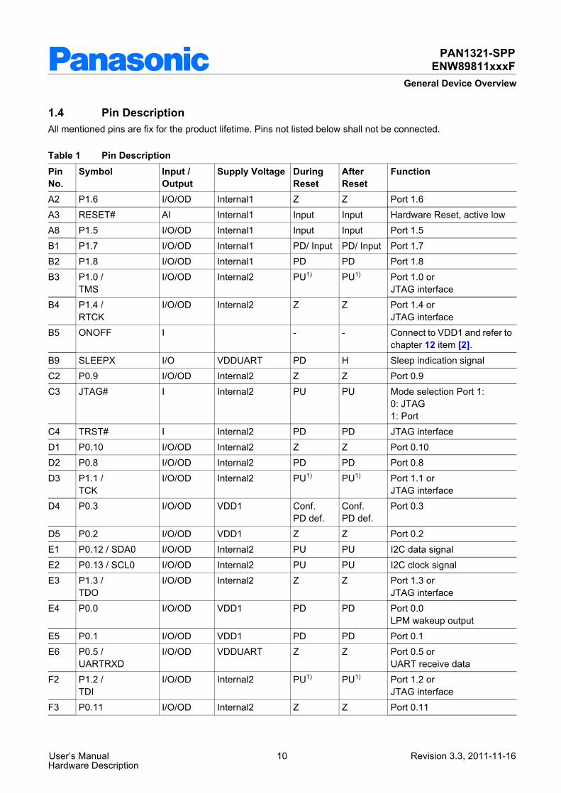
1.4 Pin DescriptionAll mentioned pins are fix for the product lifetime. Pins not listed below shall not be connected.
Table 1 Pin DescriptionPin No.
Symbol Input / Output
Supply Voltage During Reset
After Reset
Function
A2 P1.6 I/O/OD Internal1 Z Z Port 1.6A3 RESET# AI Internal1 Input Input Hardware Reset, active lowA8 P1.5 I/O/OD Internal1 Input Input Port 1.5B1 P1.7 I/O/OD Internal1 PD/ Input PD/ Input Port 1.7B2 P1.8 I/O/OD Internal1 PD PD Port 1.8B3 P1.0 /
TMSI/O/OD Internal2 PU1) PU1) Port 1.0 or
JTAG interfaceB4 P1.4 /
RTCKI/O/OD Internal2 Z Z Port 1.4 or
JTAG interfaceB5 ONOFF I - - Connect to VDD1 and refer to
chapter 12 item [2].B9 SLEEPX I/O VDDUART PD H Sleep indication signalC2 P0.9 I/O/OD Internal2 Z Z Port 0.9C3 JTAG# I Internal2 PU PU Mode selection Port 1:
0: JTAG1: Port
C4 TRST# I Internal2 PD PD JTAG interfaceD1 P0.10 I/O/OD Internal2 Z Z Port 0.10D2 P0.8 I/O/OD Internal2 PD PD Port 0.8D3 P1.1 /
TCKI/O/OD Internal2 PU1) PU1) Port 1.1 or
JTAG interfaceD4 P0.3 I/O/OD VDD1 Conf.
PD def.Conf. PD def.
Port 0.3
D5 P0.2 I/O/OD VDD1 Z Z Port 0.2E1 P0.12 / SDA0 I/O/OD Internal2 PU PU I2C data signalE2 P0.13 / SCL0 I/O/OD Internal2 PU PU I2C clock signalE3 P1.3 /
TDOI/O/OD Internal2 Z Z Port 1.3 or
JTAG interfaceE4 P0.0 I/O/OD VDD1 PD PD Port 0.0
LPM wakeup outputE5 P0.1 I/O/OD VDD1 PD PD Port 0.1E6 P0.5 /
UARTRXDI/O/OD VDDUART Z Z Port 0.5 or
UART receive dataF2 P1.2 /
TDII/O/OD Internal2 PU1) PU1) Port 1.2 or
JTAG interfaceF3 P0.11 I/O/OD Internal2 Z Z Port 0.11
User’s Manual 10 Revision 3.3, 2011-11-16Hardware Description

PAN1321-SPPENW89811xxxF
General Device Overview
Descriptions of acronyms used in the pin list:
InputOutputOutput with open drain capabilityTristatePull-upPull-downAnalog (e.g. AI means analog input)Supply (e.g. SO means supply output)
F4 P0.14 I/O VDDUART Z Z Port 0.14 LPM wakup input
F5 P0.7 / UARTCTS
I/O/OD VDDUART Z Z Port 0.7 orUART CTS flow control
F7 P0.4 / UARTTXD
I/O/OD VDDUART PU PU Port 0.4 orUART transmit data
F8 P0.6 / UARTRTS
I/O/OD VDDUART PU PU Port 0.6 orUART RTS flow control
A4, A5, A6
VSUPPLY SI - - Power supply
C1 VREG SO - - Regulated Power supplyF6 VDDUART SI - - UART interface Power supplyC5 VDD1 SI - - Power supplyA1, A7, A9, C8, C9, D7, D8, E8, E9, F1, F9
VSS - - Ground
1) Fixed pull-up/pull-down if JTAG interface is selected, not affected by any chip reset. If JTAG interface is not selected the port is tristate.
Acronym DescriptionIOODZPUPDAS
Table 1 Pin DescriptionPin No.
Symbol Input / Output
Supply Voltage During Reset
After Reset
Function
User’s Manual 11 Revision 3.3, 2011-11-16Hardware Description
PAN1321-SPPENW89811xxxF
General Device Overview
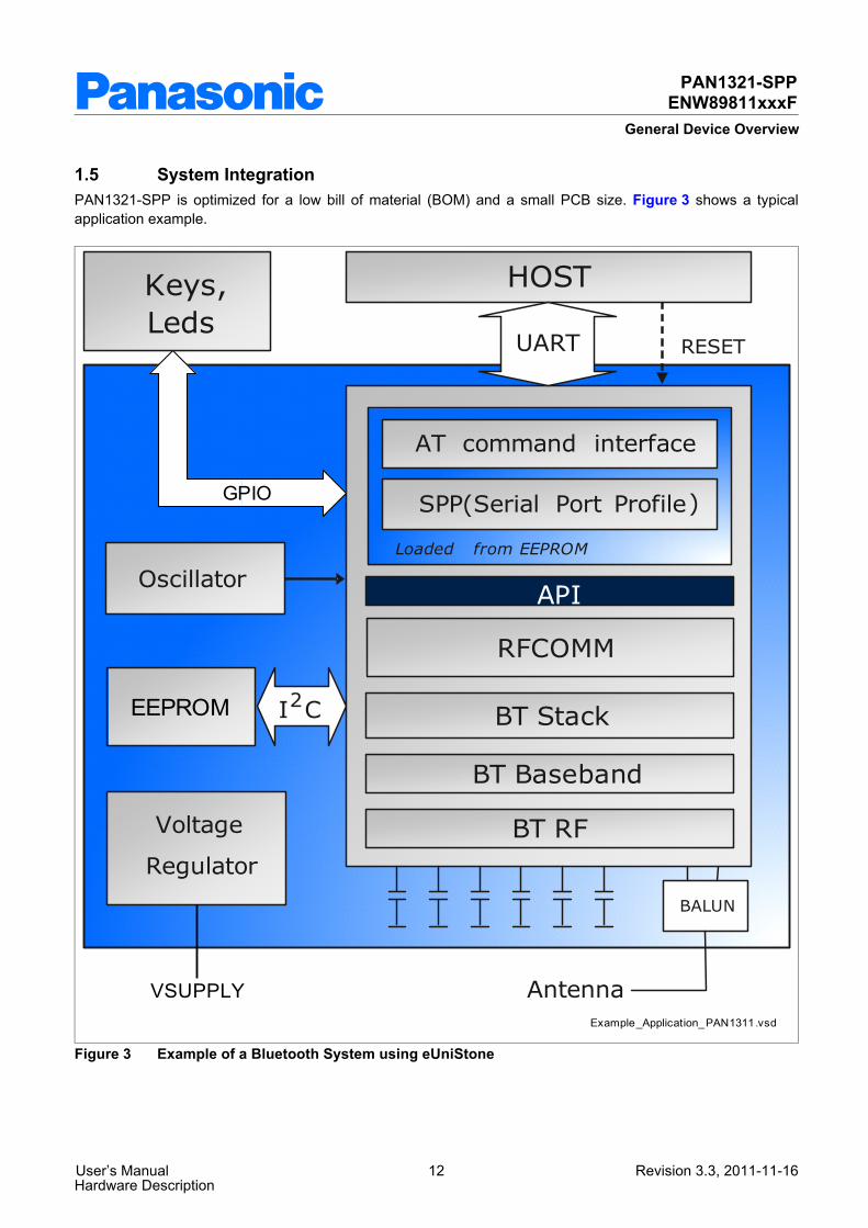
1.5 System IntegrationPAN1321-SPP is optimized for a low bill of material (BOM) and a small PCB size. Figure 3 shows a typical application example.
Example_Application_PAN1311.vsd
BT Baseband
BT Stack
RFCOMM
API
BT RF
Oscillator
HOST
I2C
BALUN
RESET
Antenna
Loaded from EEPROM
SPP(Serial Port Profile)
AT interface
UART
command
Keys,Leds
EEPROM
Voltage
Regulator
VSUPPLY
GPIO
Figure 3 Example of a Bluetooth System using eUniStone
User’s Manual 12 Revision 3.3, 2011-11-16Hardware Description
PAN1321-SPPENW89811xxxF
General Device Overview
The UART interface is used for communication between the host and PAN1321-SPP. The lines UARTTXD and UARTRXD are used for commands, events and data. The lines UARTRTS and UARTCTS are used for hardware flow control.Low power mode control of PAN1321-SPP and the host can be implemented in by using the pins P0.14 and P0.0. P0.14 is used by the host to allow PAN1321-SPP to enter low power mode and P0.0 is used by PAN1321-SPPto wake-up the host when attention is required. Additionally, the host could hardware reset PAN1321-SPP using the RESET# pin.Power is supplied to a single VSUPPLY input from which internal regulators can generate all required voltages. The UART and the GPIO’s interfaces have separate supply voltages so that they can comply with host signaling.
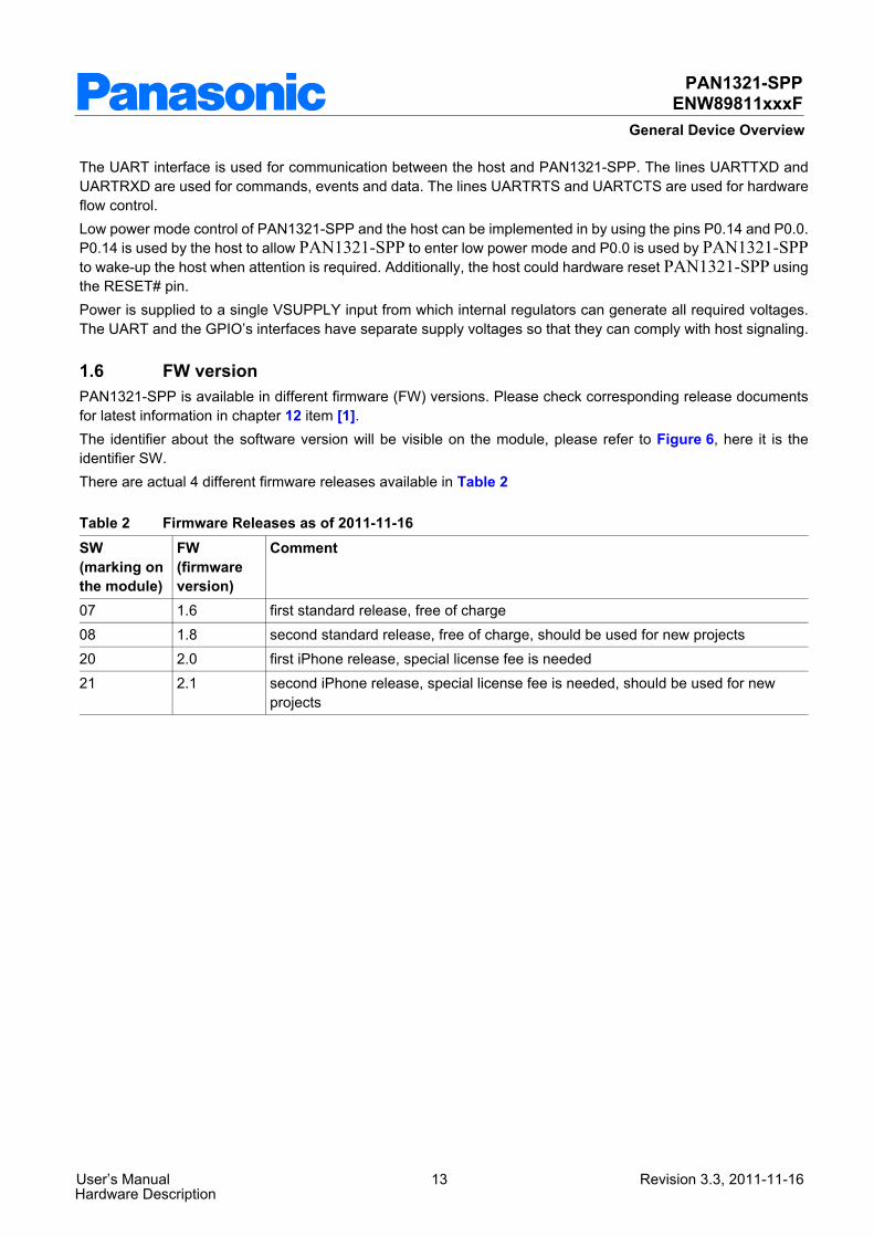
1.6 FW versionPAN1321-SPP is available in different firmware (FW) versions. Please check corresponding release documents for latest information in chapter 12 item [1]. The identifier about the software version will be visible on the module, please refer to Figure 6, here it is the identifier SW.There are actual 4 different firmware releases available in Table 2
1.6 first standard release, free of charge1.8 second standard release, free of charge, should be used for new projects2.0 first iPhone release, special license fee is needed2.1 second iPhone release, special license fee is needed, should be used for new
projects
Table 2 Firmware Releases as of 2011-11-16SW (marking on the module)
FW (firmware version)
Comment
07082021
User’s Manual 13 Revision 3.3, 2011-11-16Hardware Description

PAN1321-SPPENW89811xxxF
User’s Manual 14 Revision 3.3, 2011-11-16Hardware Description
Basic Operating Information
2 Basic Operating Information
2.1 Power SupplyPAN1321-SPP is supplied from a single supply voltage VSUPPLY. This supply voltage must always be present. The PAN1321-SPP chip is supplied from an internally generated 2.5 V supply voltage. This voltage can be accessed from the VREG pin. This voltage may not be used for supplying other components in the host system but can be used for referencing the host interfaces.The GPIO’s and the UART interface are supplied with dedicated, independent, reference levels via the VDD1 and VDDUART pins. All other digital I/O pins are supplied internally by either 2.5 V (Internal2) or 1.5 V (Internal1). Section 1.4 provides a mapping between pins and supply voltages.The I/O power domains (VDD1 and VDDUART) are completely separated from the other power domains and can stay present also in low power modes.
2.2 ClockingPAN1321-SPP contains a crystal from which the internal 26 MHz system clock is generated. Also, the low power mode clock of 32 kHz is generated internally, which means that no external clock is needed.
User’s Manual 15 Revision 3.3, 2011-11-16Hardware Description
PAN1321-SPPENW89811xxxF
Interfaces
3 Interfaces
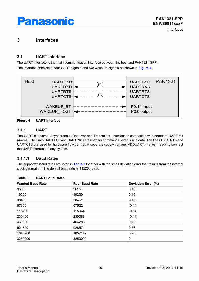
3.1 UART InterfaceThe UART interface is the main communication interface between the host and PAN1321-SPP. The interface consists of four UART signals and two wake-up signals as shown in Figure 4.
UARTTXDUARTRXDUARTRTSUARTCTS
WAKEUP_BTWAKEUP_HOST
UARTTXDUARTRXDUARTRTSUARTCTS
P0.14 inputP0.0 output
Host PAN1321
Figure 4 UART Interface
3.1.1 UARTThe UART (Universal Asynchronous Receiver and Transmitter) interface is compatible with standard UART H4 (4-wire). The lines UARTTXD and UARTRXD are used for commands, events and data. The lines UARTRTS and UARTCTS are used for hardware flow control. A separate supply voltage, VDDUART, makes it easy to connect the UART interface to any system.
3.1.1.1 Baud RatesThe supported baud rates are listed in Table 3 together with the small deviation error that results from the internal clock generation. The default baud rate is 115200 Baud.
9615 0.1619230 0.1638461 0.1657522 -0.14115044 -0.14230088 -0.14464285 0.76928571 0.761857142 0.763250000 0
Table 3 UART Baud Rates Wanted Baud Rate Real Baud Rate Deviation Error (%)960019200384005760011520023040046080092160018432003250000
PAN1321-SPPENW89811xxxF
General Device Capabilities
4 General Device CapabilitiesThis chapter describes features available in the PAN1321 (ENW89811xxxF) core.Actual feature set and how to access the features can be found in the AT Command document [1]. Release specific performance characteristics, like data speed, is related in the SW Release Notes [1].
4.1 HCI+The PAN1321 module can be programmed over UART with a specific application for RF test purposes, like TX continuous or TX burst mode. This test application is controlled over the UART through Infineon specific HCI commands. The commands supported by this test application are described in the document “T8753-2-Infineon_Specific_HCI_Commands-7600.pdf”.
4.2 Firmware ROM PatchingIn any chip with complex firmware in ROM it is wise to support patching. The risk of project delay is significantly reduced when problems can be solved without hardware changes. Enhancements, adaptations and bug fixes can be handled very late during design-in, even after the PAN1321 has been soldered in the final product.The well-proven patch concept used in PAN1321 is described below.
4.2.1 Patch SupportPAN1321-SPP contains dedicated hardware that makes it possible to apply patches to the code and data in the firmware ROM. The hardware is capable of replacing up to 32 blocks of 16 bytes each with new content. This area can be filled with any combination of code and data. The firmware patch is stored in EEPROM and automatically loaded after startup. This provides a flexible bugfix solution for the ROM part of the firmware.
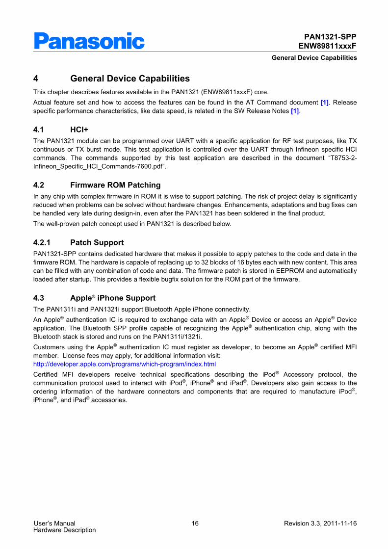
4.3 Apple® iPhone SupportThe PAN1311i and PAN1321i support Bluetooth Apple iPhone connectivity.An Apple® authentication IC is required to exchange data with an Apple® Device or access an Apple® Device application. The Bluetooth SPP profile capable of recognizing the Apple® authentication chip, along with the Bluetooth stack is stored and runs on the PAN1311i/1321i.Customers using the Apple® authentication IC must register as developer, to become an Apple® certified MFI member. License fees may apply, for additional information visit: http://developer.apple.com/programs/which-program/index.htmlCertified MFI developers receive technical specifications describing the iPod® Accessory protocol, the communication protocol used to interact with iPod®, iPhone® and iPad®. Developers also gain access to the ordering information of the hardware connectors and components that are required to manufacture iPod®, iPhone®, and iPad® accessories.
User’s Manual 16 Revision 3.3, 2011-11-16Hardware Description

PAN1321-SPPENW89811xxxF
Ordering Information
4.3.1 Apple® Authentication ChipThe below Figure 5 will give a rough overview how the hardware concept looks like, in addition the init commands are shown to establish a link between PAN1311i/1321i and the Apple® Device.
Controller
• Make Discoverable• Register Local Service• Auto Accept Requests• Connect Request• Send Stream Data• Apple Authentication Lingo
RAM
Digital I/O
I²C
Analog
PAN1321
PAN1321 Init Commands
I²C CLK
Micro-controller
Flash
I²S
USB
UART
AppleAuthenticationCoprocessor
I²C
I²C CLK
EEPROM
Voltage Regulator
Crystal26MHz
Balun Filter / Matching
I 2C
Vs upply
GPIO
UART
VDD_ UART
VDD1CeramicAntenna
PMB8753/2BlueMoon UniCellular
Figure 5 Simplified Block Diagram, when using an Apple Authentication Chip
5 Ordering InformationThis chapter shows the different order codes for the PAN1321-SPP. In case, there is no specific software version mentioned in the order, we will always deliver the latest official software release, which is downwards compatible. Please refer also to Table 2 “Firmware Releases as of 2011-11-16” on Page 13.1)
PAN1321-SPP Bluetoth 2.0 Module with integrated Antenna and a standard SPP software.PAN1321-SPP Bluetoth 2.0 Module with integrated Antenna and a spezial SPP software, which supports Apples iPhone®
1500
Table 4 Order Code as of 2011-11-16Order Code Description MOQ 1)
ENW89811K4CF 1500
ENW89811A6KF
1) Abbreviation for Minimum Order Quantity (MOQ). The standard MOQ for mass productionare 1500 pieces, fewer only on customer demand. Samples for evaluation can be deliveredat any quantity.
User’s Manual 17 Revision 3.3, 2011-11-16Hardware Description

PAN1321-SPPENW89811xxxF
Bluetooth Capabilities
6 Bluetooth Capabilities
6.1 Supported Features
• Bluetooth V2.0 + EDR compliant• Enhanced Data Rate up to 3 Mbit/s• Adaptive Frequency Hopping (AFH)• All packet types• Authentication, Pairing and Encryption• SPP Device A and B support 1 ACL link with stream or command mode• SPP Device A and B - Visible while connected• SPP Device A and B - Visible/connectable when not connected• SPP Device A and B - Device Discovery capable after receiving OK on data transfer• Sniff mode is supported with above capabilities• 5 trusted devices stored in EEPROM• Enable DUT• Crystal calibration• H4 with UART HW flow control (RTS/CTS)• Security modes: Modes 1 and Mode 3• Master-Slave role switch• Quality of Service• Channel Quality Driven Data Rate change• Sniff, Hold• Role Switch• RSSI and Power Control• Power class 2 and 3• Standard Bluetooth test mode, Active Tester Mode and RF Test Modes
User’s Manual 18 Revision 3.3, 2011-11-16Hardware Description
PAN1321-SPPENW89811xxxF
Bluetooth Capabilities
6.2 PAN1321-SPP Specifics and Extensions
6.2.1 During Connection
6.2.1.1 Role SwitchOnly one role switch can be performed at a time. If a role switch request is pending, other role switch requests on the same or other links are rejected. If a role switch fails, PAN1321-SPP will automatically try again a maximum of three times. Encryption (if present) is stopped in the old piconet before a role switch is performed and re-enabled when the role switch has succeeded or failed.
6.2.1.2 Dynamic Polling StrategyIn addition to the regular polling scheme, PAN1321-SPP dynamically assigns unused slots to links where data is exchanged. This adapts very well to bursty traffic and improves throughput and latency on the links.
6.2.1.3 Adaptive Frequency Hopping (AFH)PAN1321-SPP supports adaptive frequency hopping according to the Bluetooth 2.0 + EDR specification. AFH switch and channel classification are supported both as master and slave. Channel classification from the host is also supported.A number of HCI+ commands and events are available to provide information about AFH operation. The commands Infineon_Enable_AFH_Info_Sending and Infineon_Disable_AFH_Info_Sending turn on and off the Infineon AFH Info events that provide detailed information about channel classification, channel maps, interferers, etc.If enabled by the Infineon_Enable_Infineon_Events command, the Infineon AFH Extraordinary RSSI event informs the host whenever extraordinary RSSI measurements in unused slots have been started. This is done when the number of known good channels has decreased below a critical limit and periodically after a defined time.The Infineon_Set_AFH_Measurement_Period command can be used to configure the duration of the AFH measurement period.
6.2.1.4 Channel Quality Driven Data Rate Change (CQDDR)PAN1321-SPP supports channel quality driven data rate change according to the Bluetooth 2.0 + EDR specification. A device that receives an LMP_preferred_rate message is not required to follow all recommendations. PAN1321-SPP normally at least follows the recommendation whether to use forward error correction (FEC) or not. If possible, recommendations about packet size and modulation scheme will be taken into account. When PAN1321-SPP sends an LMP_preferred_rate to another device the proposal always includes preferences for all parameters.The HCI+ commands Infineon_Enable_CQDDR_Info_Sending and Infineon_Disable_CQDDR_Info_Sending turn on and off sending of the Infineon CQDDR Info event. This event provides information to the host every time a new CQDDR proposal is sent to a remote device.
User’s Manual 19 Revision 3.3, 2011-11-16Hardware Description

PAN1321-SPPENW89811xxxF
Bluetooth Capabilities
6.2.2 RSSI and Output Power Control
6.2.2.1 Received Signal Strength Indication (RSSI)PAN1321-SPP supports received signal strength measurements and uses LMP signaling to keep the output power of a remote device within the golden receive power range. The range is set with the BD_DATA parameters RSSI_Min and RSSI_Max.
6.2.2.2 Output Power ControlPAN1321-SPP supports power control according to the Bluetooth 2.0+EDR specification.• The output power can be controlled in up to 4 configurable steps. PAN1321-SPP can work as a class 2 or 3
device, depending on the settings.• Fine tuning can be used on the power steps.• A default sub-state power step can be setThe power step configuration is set through BD_DATA parameters.The Inquiry output power can be programmed with the Write Inquiry Transmit Power Level command introduced in the 2.0 Bluetooth Core specification.
6.2.2.3 Ultra Low Transmit PowerFor high security devices the output power can be reduced to a value that reduces the communication range to a few inches. This mode is enabled with the HCI+ command Infineon_TX_Power_Config.
User’s Manual 20 Revision 3.3, 2011-11-16Hardware Description

PAN1321-SPPENW89811xxxF
Electrical Characteristics
7 Electrical Characteristics
7.1 Absolute Maximum Ratings
Values
-40 – 125 °C –-0.3 – 6.0 V –-0.9 – 4.0 V –-0.9 – 4.0 V –-0.3 – 4.0 V VSUPPLY > 4 V-0.3 – VSUPPLY V VSUPPLY < 4 V-0.3 – VSUPPLY+0.3 V-0.9 – 4.0 V –-0.9 – 4.0 V -9– – 1.0 kV According to MIL-STD883D
method 3015.7
Note: Stresses above those listed here are likely to cause permanent damage to the device. Exposure to absolute maximum rating conditions for extended periods may affect device reliability. Maximum ratings are absolute ratings; exceeding only one of these values may cause irreversible damage to the integrated circuit. Maximum ratings are not operating conditions.
7.2 Operating Conditions
Values
-40 – 85 °C –2.9 – 4.1 V –1.35 – 3.6 V –1.35 – 3.6 V –
Table 5 Absolute Maximum Ratings Parameter Symbol Unit Note / Test Condition
Min. Typ. Max.Storage temperatureVSUPPLY supply voltageVDDUART supply voltageVDD1 supply voltageVREGVREGONOFFInput voltage rangeOutput voltage rangeESD
Table 6 Operating Conditions Parameter Symbol Unit Note / Test Condition
Min. Typ. Max.Operating temperatureMain supply voltage (Vsupply)VDDUARTVDD1
User’s Manual 21 Revision 3.3, 2011-11-16Hardware Description

PAN1321-SPPENW89811xxxF
Electrical Characteristics
7.3 DC Characteristics
7.3.1 Pad Driver and Input StagesFor more information, see Chapter 1.4.
Values
-0.3 – 0.27 V –1.15 – 3.6 V –– – 0.25 V IOL = 1 mA1.1 – – V IOH = -1 mA– – 1 mA –– – 10 pF –– 0.01 1 μA Input and output drivers
disabled
Values
-0.3 – 0.45 V –1.93 – 2.8 V P0.101.93 – 3.6 V Other pins– – 0.25 V IOL = 5 mA– – 0.15 V IOL = 2 mA2.0 – – V IOH = -5 mA2.1 – – V IOH = -2 mA– – 5 mA –– – 10 pF –– 0.01 1 μA Input and output drivers
disabled
Table 7 Internal1 (1.5 V) Supplied Pins Parameter Symbol Unit Note / Test Condition
Min. Typ. Max.Input low voltageInput high voltageOutput low voltageOutput high voltageContinuous Load1)
1) The totaled continuous load for all Internal1 supplied pins shall not exceed 2mA at the same time
Pin CapacitanceMagnitude Pin Leakage
Table 8 Internal2 (2.5 V) Supplied Pins Parameter Symbol Unit Note / Test Condition
Min. Typ. Max.Input low voltageInput high voltageInput high voltageOutput low voltageOutput low voltageOutput high voltageOutput high voltageContinuous Load1)
1) The totaled continuous load for all Internal2 supplied pins shall not exceed 35 mA at the same time
Pin CapacitanceMagnitude Pin Leakage
Table 9 VDDUART Supplied Pins Parameter Symbol Values Unit Note / Test Condition
Min. Typ. Max.Input low voltage -0.3 – 0.2*VDDUART V –Input high voltage 0.7*VDDUART – VDDUART+0.3 V P0.5/UARTRXDInput high voltage 0.7*VDDUART – 3.6 V Other pins
User’s Manual 22 Revision 3.3, 2011-11-16Hardware Description

PAN1321-SPPENW89811xxxF
Electrical Characteristics
Output low voltage – – 0.25 V IOL = 5 mA VDDUART = 2.5 V
Output low voltage – – 0.15 V IOL = 2 mA VDDUART = 2.5 V
Output high voltage VDDUART -0.25
– – V IOH = -5 mA VDDUART = 2.5 V
Output high voltage VDDUART -0.15
– – V IOH = -2 mA VDDUART = 2.5 V
Continuous Load1) – – 5 mA –Pin Capacitance – – 10 pF –Magnitude Pin Leakage – 0.01 1 μA Input and output drivers
disabled
Values
-0.3 – 0.2*VDD1 V –0.7*VDD1 – 3.6 V –– – 0.25 V IOL = 5 mA
VDD1 = 2.5 V– – 0.15 V IOL = 2 mA
VDD1 = 2.5 VVDD1 -0.25
– – V IOH = -5 mA VDD1 = 2.5 V
VDD1 -0.15
– – V IOH = -2 mA VDD1 = 2.5 V
– – 5 mA –– – 10 pF –– 0.01 1 μA Input and output drivers
disabled
Values
– – 0.7 V –1.7 – VSUPPLY V –-1 0.01 1 μA ONOFF = 0 V
1) The totaled continuous load for all VDDUART supplied pins shall not exceed 35 mA at the same time
Table 10 VDD1 Supplied Pins Parameter Symbol Unit Note / Test Condition
Min. Typ. Max.Input low voltageInput high voltageOutput low voltage
Output low voltage
Output high voltage
Output high voltage
Continuous Load1)
1) The totaled continuous load for all VDD1 supplied pins shall not exceed 35 mA at the same time
Pin CapacitanceMagnitude Pin Leakage
Table 11 ONOFF PIN Parameter Symbol Unit Note / Test Condition
Min. Typ. Max.Input low voltageInput high voltageInput current
Table 9 VDDUART Supplied Pins (cont’d)
Parameter Symbol Values Unit Note / Test ConditionMin. Typ. Max.
User’s Manual 23 Revision 3.3, 2011-11-16Hardware Description

PAN1321-SPPENW89811xxxF
Electrical Characteristics
7.3.2 Pull-ups and Pull-downs
260 740 1300 N/A N/A N/A μA Pull-up current measured with pin voltage = 0 V
Pull-down current measured with pin voltage = supply voltage
Min measured at 125°C with supply = 1.35 V
Typ. measured at 27°C with supply = 2.5V
Max measured at -40°C with supply = 3.63 V
22 130 350 23 150 380 μA
4.2 24 68 3.0 20 55 μA
1.1 6.0 17 0.75 5.0 14 μA
7.3.3 Protection CircuitsAll pins have an inverse protection diode against VSS. P0.10 has an inverse diode against Internal2. P0.5/UARTRXD has an inverse diode against VDDUART. All other pins have no diode against their supply.
Table 12 Pull-up and Pull-down Currents Pin Pull Up Current Pull Down Current Unit Conditions
Min. Typ. Max. Min. Typ. Max.P0.12 P0.13P0.0 P0.1 P0.2 P0.3P0.4 P0.5 P0.6 P0.7 P0.10 P0.8 P0.9 P0.11 P0.14 P0.15
P1.0 P1.1 P1.2 P1.3 P1.4 P1.5 P1.6 P1.7 P1.8
User’s Manual 24 Revision 3.3, 2011-11-16Hardware Description
PAN1321-SPPENW89811xxxF
Electrical Characteristics
7.3.4 System Power Consumption
Values
– – 100 mA Peak current
Note: I/O currents are not included since they depend mainly on external loads.
7.4 AC Characteristics
7.5 RF Part
7.5.1 Characteristics RF PartThe characteristics involve the spread of values to be within the specific temperature range. Typical characteristics are the median of the production.All values refers to Infineon reference design. All values will be updated after verification/Characterisation.
7.5.1.1 Bluetooth Related Specifications
Table 13 Max. Load at the Different Supply Voltages Parameter Symbol Unit Note / Test Condition
Min. Typ. Max.Vsupply
Table 14 BDR - Transmitter Part Parameter Symbol Values Unit Note / Test Condition
Min. Typ. Max.Output power (high gain) 0.5 2.5 4.5 dBm Default settingsOutput power (highest gain) – 4.5 – dBm Maximum settingsPower control step size 4 6 8 dB –Frequency range fL 2400 2401.3 – MHz –Frequency range fH – 2480.7 2483.5 MHz –20 dB bandwidth – 0.930 1 MHz –2nd adjacent channel power – -40 -20 dBm –3rd adjacent channel power – -60 -40 dBm –>3rd adjacent channel power – -64 -40 dBm Max. 2 of 3 exceptions @
52 MHz offset might be usedAverage modulation deviation for 00001111 sequence
140 156 175 kHz –
Minimum modulation deviation for 01010101 sequence
115 145 – kHz –
Ratio Deviation 01010101 / Deviation 00001111
0.8 1 – –
Initial carrier frequency tolerance |foffset|
– – 75 kHz –
User’s Manual 25 Revision 3.3, 2011-11-16Hardware Description

PAN1321-SPPENW89811xxxF
Electrical Characteristics
Carrier frequency drift (one slot) |fdrift|
– 10 25 kHz –
Carrier frequency drift (three slots) |fdrift|
– 10 40 kHz –
Carrier frequency drift (five slots) |fdrift|
– 10 40 kHz –
Carrier frequency driftrate (one slot) |fdriftrate|
– 5 20 kHz/50 ms –
Carrier frequency driftrate (three slots) |fdriftrate|
– 5 20 kHz/50 ms –
Carrier frequency driftrate (five slots) |fdriftrate|
– 5 20 kHz/50 ms –
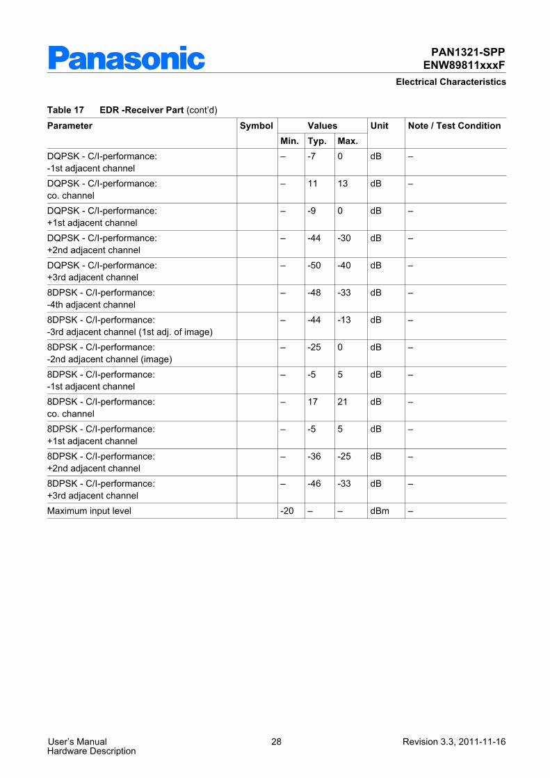
Table 15 BDR -Receiver Part Parameter Symbol Values Unit Note / Test Condition
Min. Typ. Max.Sensitivity – -86 -81 dBm Ideal wanted signalC/I-performance: -4th adjacent channel
– -51 -40 dB –
C/I-performance: -3rd adjacent channel (1st adj. of image)
– -46 -20 dB –
C/I-performance: -2nd adjacent channel (image)
– -35 -9 dB –
C/I-performance: -1st adjacent channel
– -4 0 dB –
C/I-performance: co. channel – 9 11 dB –C/I-performance: +1st adjacent channel
– -4 0 dB –
C/I-performance: +2nd adjacent channel
– -40 -30 dB –
C/I-performance: +3rd adjacent channel
– -50 -40 dB –
Blocking performance 30 MHz - 2 GHz
10 – – dBm Some spurious responses, but according to BT-specification
Blocking performance 2 GHz - 2.4 GHz
-27 – – dBm –
Blocking performance 2.5 GHz - 3 GHz
-27 – – dBm –
Blocking performance 3 GHz - 12.75 GHz
10 – – dBm Some spurious responses, but according to BT-specification
Table 14 BDR - Transmitter Part (cont’d)
Parameter Symbol Values Unit Note / Test ConditionMin. Typ. Max.
User’s Manual 26 Revision 3.3, 2011-11-16Hardware Description

PAN1321-SPPENW89811xxxF
Electrical Characteristics
Intermodulation performance -39 -34 – dBm Valid for all intermodulation testsMaximum input level -20 – – dBm –
Values
-2.5 – 2 dBm-4 -0.6 1 dB
– – 75 kHz –– – 75 kHz –– 2 10 kHz –– 10 20 % –– 10 13 % –– 20 35 % –– 20 25 % –– – 30 % –– – 20 % –99 100 – % –– -40 -26 dBc –– – -20 dBm Carrier power measured at basic
rate– – -40 dBm Carrier power measured at basic
rate
Table 16 EDR - Transmitter Part Parameter Symbol Unit Note / Test Condition
Min. Typ. Max.Output power (high gain)Relative transmit power: PxPSK - PGFSKCarrier frequency stability |ωi|Carrier frequency stability |ωi+ω0|Carrier frequency stability |ω0|DPSK - RMS DEVM8DPSK - RMS DEVMDPSK - Peak DEVM8DPSK - Peak DEVMDPSK - 99% DEVM8DPSK - 99% DEVMDifferential phase encoding1st adjacent channel power2nd adjacent channel power
3rd adjacent channel power
Table 17 EDR -Receiver Part Parameter Symbol Values Unit Note / Test Condition
Min. Typ. Max.DQPSK-Sensitivity – -88 -83 dBm Ideal wanted signal8DPSK-Sensitivityl – -83 -77 dBm Ideal wanted signalDQPSK - BER Floor Sensitivity – -84 -60 dBm –8DPSK - BER Floor Sensitivity – -79 -60 dBm –DQPSK - C/I-performance: -4th adjacent channel
– -53 -40 dB –
DQPSK - C/I-performance: -3rd adjacent channel (1st adj. of image)
– -47 -20 dB –
DQPSK - C/I-performance: -2nd adjacent channel (image)
– -31 -7 dB –
Table 15 BDR -Receiver Part (cont’d)
Parameter Symbol Values Unit Note / Test ConditionMin. Typ. Max.
User’s Manual 27 Revision 3.3, 2011-11-16Hardware Description
PAN1321-SPPENW89811xxxF
Electrical Characteristics
DQPSK - C/I-performance: -1st adjacent channel
– -7 0 dB –
DQPSK - C/I-performance: co. channel
– 11 13 dB –
DQPSK - C/I-performance: +1st adjacent channel
– -9 0 dB –
DQPSK - C/I-performance: +2nd adjacent channel
– -44 -30 dB –
DQPSK - C/I-performance: +3rd adjacent channel
– -50 -40 dB –
8DPSK - C/I-performance: -4th adjacent channel
– -48 -33 dB –
8DPSK - C/I-performance: -3rd adjacent channel (1st adj. of image)
– -44 -13 dB –
8DPSK - C/I-performance: -2nd adjacent channel (image)
– -25 0 dB –
8DPSK - C/I-performance: -1st adjacent channel
– -5 5 dB –
8DPSK - C/I-performance: co. channel
– 17 21 dB –
8DPSK - C/I-performance: +1st adjacent channel
– -5 5 dB –
8DPSK - C/I-performance: +2nd adjacent channel
– -36 -25 dB –
8DPSK - C/I-performance: +3rd adjacent channel
– -46 -33 dB –
Maximum input level -20 – – dBm –
Table 17 EDR -Receiver Part (cont’d)
Parameter Symbol Values Unit Note / Test ConditionMin. Typ. Max.
User’s Manual 28 Revision 3.3, 2011-11-16Hardware Description
PAN1321-SPPENW89811xxxF
Package Information
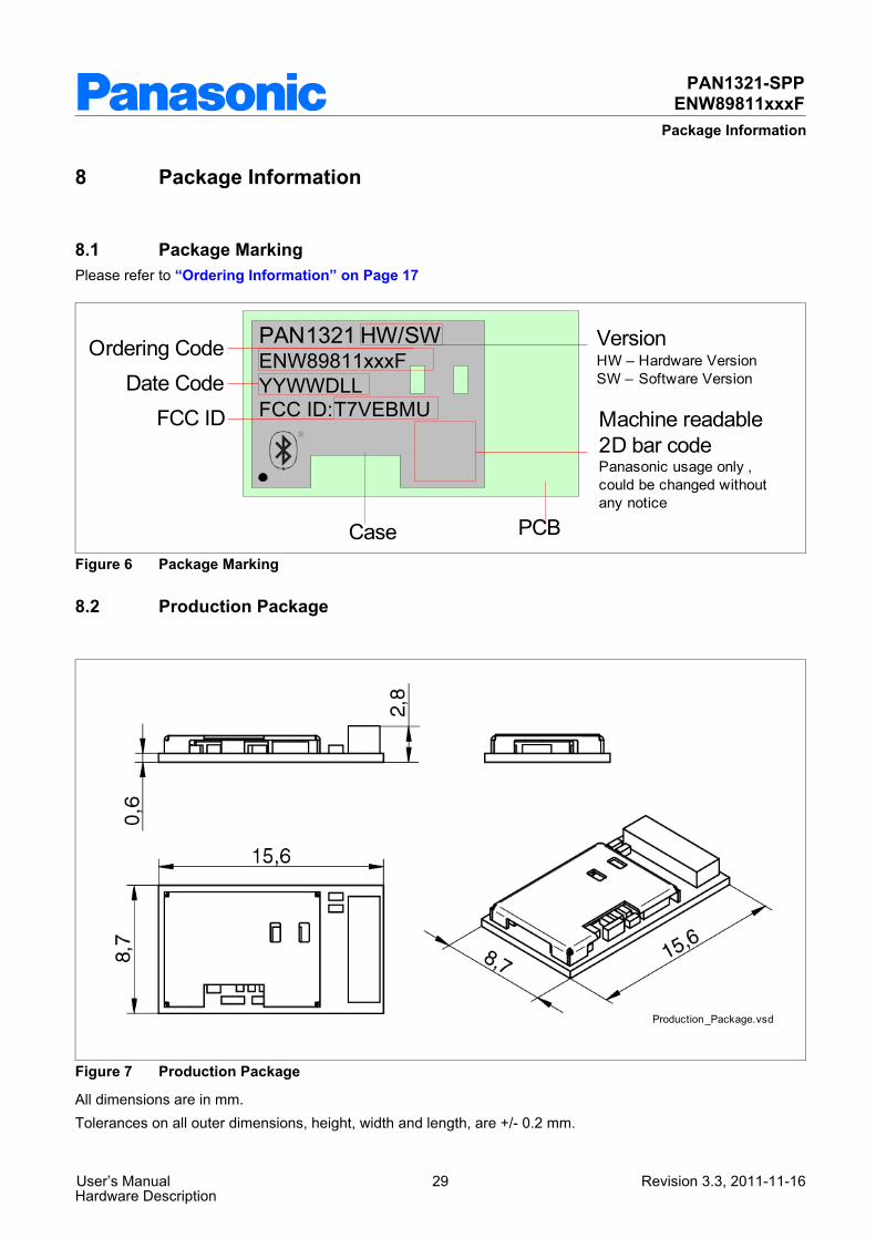
8 Package Information
8.1 Package MarkingPlease refer to “Ordering Information” on Page 17
PAN1321ENW89811xxxFYYWWDLLFCC ID:T7VEBMU
VersionHW – Hardware VersionSW – Software Version
Ordering CodeDate Code
FCC ID Machine readable2D bar codePanasonic usage only , could be changed without any notice
Case PCB
HW/SW
Figure 6 Package Marking
8.2 Production Package
Production_Package.vsd
Figure 7 Production Package
All dimensions are in mm.Tolerances on all outer dimensions, height, width and length, are +/- 0.2 mm.
User’s Manual 29 Revision 3.3, 2011-11-16Hardware Description
PAN1321-SPPENW89811xxxF
Package Information
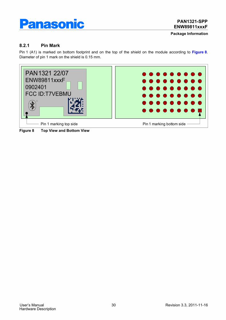
8.2.1 Pin MarkPin 1 (A1) is marked on bottom footprint and on the top of the shield on the module according to Figure 8. Diameter of pin 1 mark on the shield is 0.15 mm.
Pin 1 marking bottom side
PAN1321 22/07ENW89811xxxF0902401FCC ID:T7VEBMU
F2F3F4F5F6
E1E2E3E4E5E6E7E8E9
D1D2D3D4D5D6D7D8
C1C2C3C4C5C6C7C8
B1B2B3B4B5B6B7B8B9
A2A3A4A5A6A7A8 A1
F9 F7 F1F8
D9
C9
A9
Pin 1 marking top side
Figure 8 Top View and Bottom View
User’s Manual 30 Revision 3.3, 2011-11-16Hardware Description
PAN1321-SPPENW89811xxxF
Important Application Information
9 Important Application Information
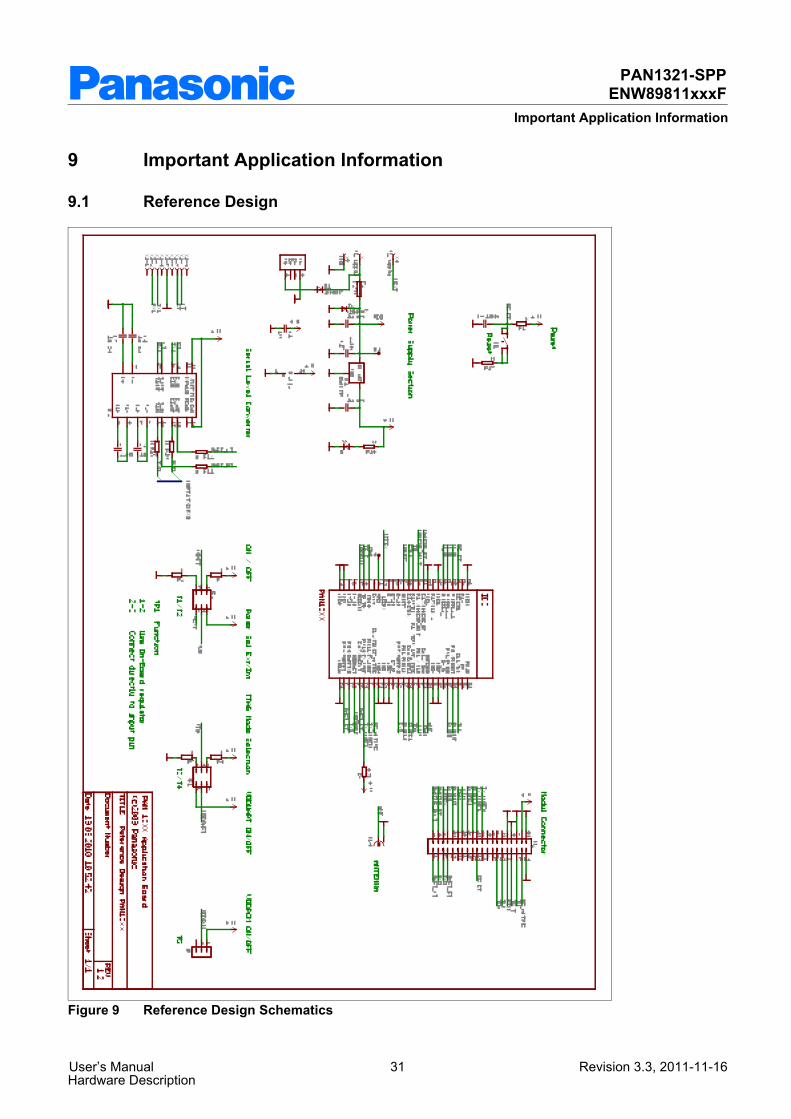
9.1 Reference Design
Figure 9 Reference Design Schematics
User’s Manual 31 Revision 3.3, 2011-11-16Hardware Description

PAN1321-SPPENW89811xxxF
Important Application Information
ENW89811xxxF is intended to be installed inside end user equipment. ENW89811xxxF is Bluetoooth-qualified and also FCC-certified and Industry Canada approved, and conforms to R&TTE (European) requirements and directives with the reference design described in Figure 9. FCC certification is valid together with the following antennas, having in mind, that this module has the Johansson antenna included:
Titanis Swivel 4 dBi 50 ohmP/N 1513151-1 Module 4 dBi 50 ohmLDA312G7313F-237 Ceramic chip 0 dBi 50 ohm
Printed inverted F Antenna (PIFA)
4 dBi 50 ohm
2450AT43A100 Ceramic chip antenna 2 dBi 50 ohmBST-2450 Dipole antenna 2 dBi 50 ohm
When using any of the above antennas, installed in the appropriate manner, it is possible to re-use the approvals for the end-product. It is, however, required to have a written consent from Infineon Technologies AG to re-use the regulatory approvals for the FCC, Canada and Europe.Manufacturers of mobile, fixed or portable devices incorporating this device are advised to clarify any regulatory questions and to have their complete product tested and approved for compliance (FCC or other when applicable). When using other antennas, a “class II permissive change” is required for FCC approval. The normal procedure is to first provide a technical test report showing that 4 dBi is not exceeded and to continue working with a regulatory test house to finalize the approval for a new antenna implementation.There are no parts in ENW89811xxxF that can be modified by the user except modifications of the device BD data and loading of SW patches. Any changes or modifications made to this device that are not expressly approved by Infineon, may void the user’s authority to operate the equipment.
9.2 FCC Class B Digital Devices Regulatory NoticeThis equipment has been tested and found to comply with the limits for a Class B digital device, pursuant to Part 15 of the FCC Rules. These limits are designed to provide reasonable protection against harmful interference in a residential installation. This equipment generates, uses, and can radiate radio frequency energy and, if not installed and used in accordance with the instructions, may cause harmful interference to radio communications. However, there is no guarantee that interference will not occur in a particular installation. If this equipment does cause harmful interference to radio or television reception, which can be determined by turning the equipment off and on, the user is encouraged to try to correct the interference by 1 or more of the following measures:• Reorient or relocate the antenna• Increase the separation between the equipment and receiver• Connect the equipment into an outlet on a circuit different from that to which the receiver is connected• Consult the dealer or an experienced radio or television technician for help
9.3 FCC Wireless NoticeThis product emits radio frequency energy, but the radiated output power of this device is far below the FCC radio frequency exposure limits. Nevertheless, the device should be used in such a manner that the potential for human contact with the antenna during normal operation is minimized.To meet the FCC's RF exposure rules and regulations:• The system antenna used for this transmitter must not be co-located or operating in conjunction with any other
antenna or transmitter.
Table 18 AntennasManufacturer Model Type Peak antenna gain ImpedanceGigAntTyco ElectronicsMurataInfineon reference design
JohanssonInwave
User’s Manual 32 Revision 3.3, 2011-11-16Hardware Description

PAN1321-SPPENW89811xxxF
Important Application Information
• The system antenna used for this module must not exceed 4 dBi.• Users and installers must be provided with antenna installation instructions and transmitter operating
conditions for satisfying RF exposure compliance.Manufacturers of mobile, fixed or portable devices incorporating this module are advised to clarify any regulatory questions and to have their complete product tested and approved for FCC compliance.
9.4 FCC Interference StatementThis device complies with Part 15 of the FCC Rules. Operation is subject to the following two conditions:1. This device may not cause harmful interference2. This device must accept any interference received, including interference that may cause undesired operation.
9.5 FCC IdentifierFCC ID: T7VEBMU
9.6 European R&TTE Declaration of ConformityHereby, Panasonic Electronic Devices Europe GmbH, declares that the Bluetooth module ENW89811xxxF is in compliance with the essential requirements and other relevant provisions of Directive 1999/5/EC.As a result of the conformity assessment procedure described in Annex III of the Directive 1999/5/EC, the end-customer equipment should be labelled as follows:
Figure 10 Equipment Label
PAN1321 in the specified reference design can be used in the following countries:Austria, Belgium, Cyprus, Czech Republic, Denmark, Estonia, Finland, France, Germany, Greece, Hungary, Ireland, Italy, Latvia, Lithuania, Luxembourg, Malta, Poland, Portugal, Slovakia, Slovenia, Spain, Sweden, The Netherlands, the United Kingdom, Switzerland, and Norway.
User’s Manual 33 Revision 3.3, 2011-11-16Hardware Description

PAN1321-SPPENW89811xxxF
Important Application Information
We, Panasonic Electronic Devices Europe GmbH
High Frequency Products Business Group
Zeppelinstrasse 19, 21337 Lueneburg, Germany
declare under our sole responsibility that the product:
Type of equipment: Bluetooth 2.0+EDR Module
Brand name: PAN1321 / PAN1311
Model name: ENW89811K4CF / ENW89810K5CF
to which this declaration relates, is in compliance with all the applicable essentialrequirements, and other provisions of the European Council Directive:
The conformity assessment procedure used for this declaration is Annex IV of this Directive.
Product compliance has been demonstrated on the basis of:
For article 3.1 (a) : Health and Safety of the User
For article 3.1 (b) : Electromagnetic Compatibility
The technical contruction file is kept available at:
Panasonic Electronic Devices Europe GmbH, Zeppelinstrasse 19, 21337 Lueneburg, Germany
Issued on: 31st of March 2010
Signed by the manufacturer:
(Company name) Panasonic Electronic Devices Europe GmbH
(Signature)
(Printed name) Heino Kaehler
(Title) Manager Wireless Modules
For article 3.2 : Effective use of spectrum allocated- EN 300 328 V1.6.1 (2004-11)- EN 300 328 V1.7.1 (2006-10)
- IEC 60950-1 (2006)
- EN 301 489-1 V1.8.1- EN 301 489-17 V2.1.1
Declaration of Conformity (DoC)1999/5/EC
1999/5/EC Radio and Telecommunications Terminal Equipment Directive (R&TTE)
Figure 11 Declaration of Conformity
User’s Manual 34 Revision 3.3, 2011-11-16Hardware Description

PAN1321-SPPENW89811xxxF
Important Application Information
9.7 Bluetooth Qualified Design IDPanasonic has submitted End Product Listing (EPL) for PAN1321, based on Infineon eBMU plattform, in the Qualified Product List of the Bluetooth SIG. These EPL are referring the Bluetooth qualfication of the SPP-AT application running on the eBMU chip under QD ID B014433.Manufacturers of Bluetooth devices incorporating PAN1321can reference the same QD ID number.Bluetooth QD ID: B014433 (PAN1321 SPP BT2.0).
9.8 Industry Canada CertificationPAN1321 complies with the regulatory requirements of Industry Canada (IC), license: IC: 216Q-EBMUManufacturers of mobile, fixed or portable devices incorporating this module are advised to clarify any regulatory questions and ensure compliance for SAR and/or RF exposure limits. Users can obtain Canadian information on RF exposure and compliance from www.ic.gc.ca.This device has been designed to operate with the antennas listed in Table 18 above, having a maximum gain of 4.0 dBi. Antennas not included in this list or having a gain greater than 4.0 dBi are strictly prohibited for use with this device. The required antenna impedance is 50 ohms. The antenna used for this transmitter must not be co-located or operating in conjunction with any other antenna or transmitter.
9.9 Label Design of the Host ProductIt is recommended to include the following information on the host product label:Contains transmitter Module FCC ID: T7VEBMU / IC: 216QEBMU
9.10 Regulatory Test HouseThe test house used by Panasonic in the Bluetooth and Regulatory approvals for the module PAN1321:Eurofins Product Service GmbHStorkower Str. 38cD-15526 Reichenwalde b. BerlinGERMANYTel.: +49 33631 888 0Fax: +49 33631 888 650www.eurofins.com
User’s Manual 35 Revision 3.3, 2011-11-16Hardware Description
PAN1321-SPPENW89811xxxF
Assembly Guidelines
10 Assembly GuidelinesThe target of this document is to provide guidelines for customers to successfully introduce the PAN1321-SPPmodule in production. This includes general description, PCB-design, solder printing process, assembly, soldering process, rework and inspection.
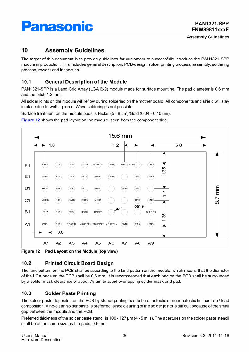
10.1 General Description of the ModulePAN1321-SPP is a Land Grid Array (LGA 6x9) module made for surface mounting. The pad diameter is 0.6 mm and the pitch 1.2 mm.All solder joints on the module will reflow during soldering on the mother board. All components and shield will stay in place due to wetting force. Wave soldering is not possible.Surface treatment on the module pads is Nickel (5 - 8 µm)/Gold (0.04 - 0.10 µm).Figure 12 shows the pad layout on the module, seen from the component side.
1.0
8.7
mm
5.0
0.6
1.35
1.35
1.2
1.2
15.6 mm
E1
D1
C1
B1
F1
A1
A2 A3 A4 A5 A6 A7 A8A1 A9
GND RESET#P1.6 P1.5VSUPPLY VSUPPLYVSUPPLY GND GND
P1 .7 TMSP1.8 ONOFFRTCK SLEEPX
VREG JTAG#P0.9 GNDVDD1TRST# GND
P0 .10 TCKP0.8 GNDP0.2P0 .3 GND
SDA0 TDOSCL0 GNDP0.1 UARTRXDP0 .0 GND
GND P0.11TDI UARTRTSUARTCTS VDDUARTP0 .14 UARTTXD GND
Ø0.6
Figure 12 Pad Layout on the Module (top view)
10.2 Printed Circuit Board DesignThe land pattern on the PCB shall be according to the land pattern on the module, which means that the diameter of the LGA pads on the PCB shall be 0.6 mm. It is recommended that each pad on the PCB shall be surrounded by a solder mask clearance of about 75 µm to avoid overlapping solder mask and pad.
10.3 Solder Paste PrintingThe solder paste deposited on the PCB by stencil printing has to be of eutectic or near eutectic tin leadfree / lead composition. A no-clean solder paste is preferred, since cleaning of the solder joints is difficult because of the small gap between the module and the PCB.Preferred thickness of the solder paste stencil is 100 - 127 µm (4 - 5 mils). The apertures on the solder paste stencil shall be of the same size as the pads, 0.6 mm.
User’s Manual 36 Revision 3.3, 2011-11-16Hardware Description
PAN1321-SPPENW89811xxxF
Assembly Guidelines
10.4 Assembly
10.4.1 Component PlacementIn order to assure a high yield, good placement on the PCB is necessary. As a rule of thumb the tolerable misplacement is 150 µm. This means that the PAN1321 module can be assembled with a variety of placement systems.It is recommended to use a vision system capable of package pad recognition and alignment that evaluates the pad locations on the package (in contrast to outline centring). This eliminates the pad to package edge tolerance.The recommendation is to pick and place the module with a nozzle in the centre of the shield. The nozzle diameter shall not be bigger than 4 mm.
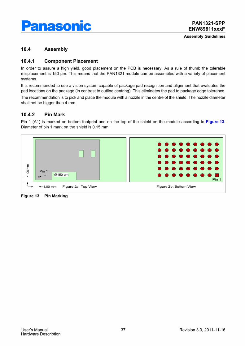
10.4.2 Pin MarkPin 1 (A1) is marked on bottom footprint and on the top of the shield on the module according to Figure 13. Diameter of pin 1 mark on the shield is 0.15 mm.
F2F3F4F5F6
E1E2E3E4E5E6E7E8E9
D1D2D3D4D5D6D7D8
C1C2C3C4C5C6C7C8
B1B2B3B4B5B6B7B8B9
A2A3A4A5A6A7A8 A1
F9 F7 F1F8
D9
C9
A9
Pin 1
Figure 2a: Top View Figure 2b: Bottom View1,00 mm
Ø150 µm1.00
mm
Pin 1
Figure 13 Pin Marking
User’s Manual 37 Revision 3.3, 2011-11-16Hardware Description
PAN1321-SPPENW89811xxxF
Assembly Guidelines
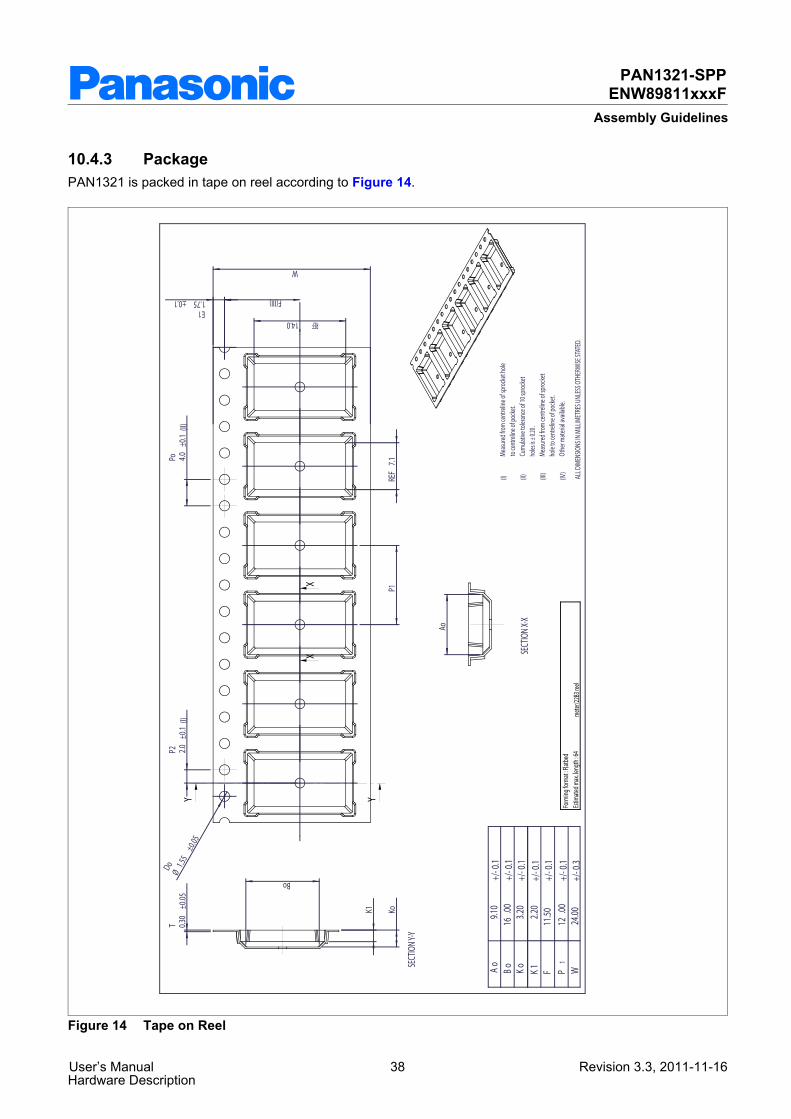
10.4.3 PackagePAN1321 is packed in tape on reel according to Figure 14.
Figure 14 Tape on Reel
User’s Manual 38 Revision 3.3, 2011-11-16Hardware Description
PAN1321-SPPENW89811xxxF
Assembly Guidelines
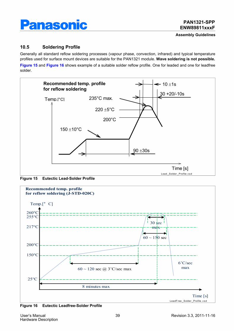
10.5 Soldering ProfileGenerally all standard reflow soldering processes (vapour phase, convection, infrared) and typical temperature profiles used for surface mount devices are suitable for the PAN1321 module. Wave soldering is not possible.Figure 15 and Figure 16 shows example of a suitable solder reflow profile. One for leaded and one for leadfree solder.
Lead _Solder _Prof ile .v s d
Recommended temp. profile for reflow soldering
Temp.[°C]
Time [s]
235°C max.
220 ±5°C
200°C
150 ±10°C
90 ±30s
10 ±1s
30 +20/-10s
Figure 15 Eutectic Lead-Solder Profile
LeadF ree _Solder _Prof ile .v s d
25°C
150°C
200°C
217°C
255°C 260°C
60 ~ 120 sec @ 3’C/sec max
60 ~ 150 sec
30 sec max
6’C/sec max
8 minutes max
Temp.[° C]
Time [s]
Recommended temp. profile for reflow soldering (J-STD-020C)
Figure 16 Eutectic Leadfree-Solder Profile
User’s Manual 39 Revision 3.3, 2011-11-16Hardware Description
PAN1321-SPPENW89811xxxF
Assembly Guidelines
At the reflow process each solder joint has to be exposed to temperatures above solder liquids for a sufficient time to get the optimum solder joint quality, whereas overheating the board with its components has to be avoided. Using infrared ovens without convection special care may be necessary to assure a sufficiently homogeneous temperature profile for all solder joints on the PCB (especially on large, complex boards with different thermal masses of the components). The most recommended types are therefore forced convection or vapour phase reflow. Nitrogen atmosphere can generally improve solder joint quality, but is normally not necessary.The reflow profiles and other reflow parameters are dependent on the used solder paste. The paste manufacturer provides a reflow profile recommendation for this product.Additionally it is important not to overheat the PAN1321 module by a too large reflow peak temperature. PAN1321contain several plastic packages and is there by sensitive of the moisture content level at the time of board assembly.Overheating in combination with excessive moisture content could result in package delaminations or cracks (popcorn effect). The heating rate should not exceed 3°C/s and max sloping rate should not exceed 4°C/s.PAN1321 shall be handled according to MSL3, which means a floor life of 168h in 30°C/60% r.h.The PAN1321 module can be soldered according to max. J-STD-020C curve, assuming that all other conditions are followed stated in Product Specification, Qualification Report and in Application Note. Restriction is that PAN1321 can be soldered two times, since one time is already consumed when soldering devices on Module.
10.6 Rework
10.6.1 Removal Procedure
1. Heat the module with an appropriate heating nozzle according to the instruction of the equipment or on a hot plate (about 225°C dependent on the board). Hot plate can only be used if the board is single side assembled. The temperature of the module shall be 200-220°C.
2. Use grippers or a pair of tweezers to remove the module. The module has to be gripped on two opposite edges of the module (not on the shield).
3. Remove excess solder by using solder sucker, suction soldering irons or solder wick.
10.6.2 Replacement ProcedureReplacement can be done in two ways, dependent of how the solder is applied. Solder can be applied either by dispensing on the mother board or by printing the solder paste directly on the module.
10.6.2.1 Alternative 1: Dispensing SolderA dispenser with controlled volume must be used to assure the same volume on every pad. The volume on each pad shall be about 0.04 mm3.1. Dispense 0.04 mm3 on each LGA pad2. Pick the module by a nozzle and place in the right position on the board3. Reflow the solder.
User’s Manual 40 Revision 3.3, 2011-11-16Hardware Description
PAN1321-SPPENW89811xxxF
Assembly Guidelines
10.6.2.2 Alternative 2: Printing SolderTo print solder on the module a fixture must be used. The purpose of the fixture is to get a flat surface and fix the stencil and module for printing. An example of how this fixture can be designed is shown in Figure 17.
Solder _Print ing .v s d
Vacuum hol es
Solder paste stencil
C avity of the module Tooling pins
B ottom
Fixture
Figure 17 Solder Printing
1. Assemble the fixture to the bottom2. Place the module in the cavity with the LGA pads upwards3. Place the solder paste stencil on the fixture and make sure it fits to the tooling pins and the module4. Apply vacuum to fix the solder paste stencil5. Apply solder paste on the stencil and print by using a blade6. Turn everything (bottom, fixture and stencil) upside down.7. Separate carefully the bottom from the fixture8. Pick the module by a nozzle and place in the right position on the board9. Reflow the solder.
10.7 InspectionAutomatic inspection of the solder paste printing before assembly is highly recommended to ensure high yield and good long term reliability.
10.8 Component SalvageIf it is intended to send a defect PAN1321 module back to the supplier for failure analysis, please note that during the removal of this component no further defects must be introduced to the device, because this may hinder the failure analysis at the supplier. This includes ESD precautions, not to apply high mechanical force for component removal, and to prevent excess moisture content in the package during salvage (risk of pop corning failures). Therefore if the maximum storage time out of the dry pack (see label on packing material) is exceeded after board assembly, the PCB has to be dried 24h at 125°C before soldering off the defect component, because otherwise too much moisture may have been accumulated.
User’s Manual 41 Revision 3.3, 2011-11-16Hardware Description

PAN1321-SPPENW89811xxxF
Assembly Guidelines
10.9 Voids in the Solder Joints
10.9.1 Expected Void Content and ReliabilityThe content of voids is larger on LGA modules than for modules with BGA or leads. At a LGA solder joint the outgassing flux has a longer way to the surface of the solder and it has a relatively small surface to the air.The void content of the PAN1321 module conforms to IPC-A-610D (25% or less voiding area/area).Figure 18 shows an example of void-content at a module assembled at production site. Normally you can see the whole spectra of void content variation within the same lot and occasion of assembly.
Voids _IPC _A_ 610D .v s d
Figure 18 X-ray Picture Showing Voids Conforming to IPC-A-610D
10.9.2 Parameters with an Impact on VoidingIf the void content has to be reduced following parameters have an impact.
Solderability on module and PCBBad solderability is often connected to oxidation and has therefore a major impact on voiding. Flux will get entrapped on oxidized surfaces. In general, Ni/Au pads show fewer voids than HASL and OSP.
Solder pasteHigher activity of the flux will remove oxide rapidly and less flux will get entrapped.Voiding increases with increasing solder paste exposure time, since long exposure time will result in more oxidation and moisture pickup.
Pad sizeA large soldering pad means that the outgassing flux has a longer way to the surface of the solder, and will thereby create more voids.
Solder pasteSmaller powder size and higher metal load means more metal surface to deoxidize and thereby more entrapped flux and voiding. Higher metal load does also mean higher viscosity and more difficult for outgassed flux to remove from the solder.
User’s Manual 42 Revision 3.3, 2011-11-16Hardware Description

PAN1321-SPPENW89811xxxF
Assembly Guidelines
Stencil thicknessA thick solder paste stencil means more surface area to the air and thereby easier for the outgassing flux to leave the solder.
Temperature soldering profileToo short preheat time means that the flux does not get enough time to react and flux get entrapped in the solder and create voids.Too long reflow time gives larger voidsToo short reflow time gives a fraction of voids
User’s Manual 43 Revision 3.3, 2011-11-16Hardware Description
PAN1321-SPPENW89811xxxF
Terminology
11 Terminology
AACK AcknowledgementACL Asynchronous Connection-oriented (logical transport)AFH Adaptive Frequency HoppingAHS Adaptive Hop SequenceARQ Automatic Repeat reQuestBb bit/bits (e.g. kb/s)B Byte/Bytes (e.g. kB/s)BALUN BALanced UNbalancedBD_ADDR Bluetooth Device AddressBER Bit Error RateBMU BlueMoon UniversalBOM Bill Of MaterialBT BluetoothBW BandwidthCCMOS Complementary Metal Oxide SemiconductorCOD Class Of DeviceCODEC COder/DECoderCPU Central Processing UnitCQDDR Channel Quality Driven Data RateCRC Cyclic Redundancy CheckCTS Clear To Send (UART flow control signal)CVSD Continuous Variable Slope Delta (modulation)CDCT Clock Drift Compensation TaskCQDDR Channel Quality Driven Data RateDDC Direct CurrentDDC Device Data ControlDM Data Medium-Rate (packet type)DMA Direct Memory AccessDH Data High-Rate (packet type)DPSK Differential Phase Shift Keying (modulation)DQPSK Differential Quaternary Phase Shift Keying (modulation)DSP Digital Signal ProcessorDUT Device Under Test
User’s Manual 44 Revision 3.3, 2011-11-16Hardware Description
PAN1321-SPPENW89811xxxF
Terminology
EEDR Enhanced Data RateEEPROM Electrically Erasable Programmable Read Only MemoryeSCO Extended Synchronous Connection-Oriented (logical transport)EV Extended Voice (packet type)FFEC Forward Error CorrectionFHS Frequency Hop Synchronization (packet)FIFO First In First Out (buffer)FM Frequency ModulationFW FirmwareGGFSK Gaussian Frequency Shift Keying (modulation)GPIO General Purpose Input/OutputGSM Global System for Mobile communicationHHCI Host Controller InterfaceHCI+ Infineon Specific HCI command setHEC Header Error CheckHV High quality Voice (packet type)HW HardwareII2C Inter-IC Control (bus)I2S Inter-IC Sound (bus)IAC Inquiry Access CodeID IDentifierIEEE Institute of Electrical and Electronics EngineersIF Intermediate FrequencyISM Industrial Scientific & Medical (frequency band)JJTAG Joint Test Action GroupLLAN Local Area NetworkLAP Lower Address PartLM Link ManagerLMP Link Manager ProtocolLNA Low Noise AmplifierLO Local OscillatorLPM Low Power Mode(s)LPO Low Power Oscillator
User’s Manual 45 Revision 3.3, 2011-11-16Hardware Description
PAN1321-SPPENW89811xxxF
Terminology
LSB Least Significant Bit/ByteLT_ADDR Logical Transport AddressMMSB Most Significant Bit/ByteMSRS Master-Slave Role SwitchNNC No ConnectionNOP No OPerationNVM Non-Volatile MemoryOOCF Opcode Command FieldOGF Opcode Group FieldPPA Power AmplifierPCB Printed Circuit BoardPCM Pulse Coded ModulationPDU Protocol Data UnitPER Packet Error RatePIN Personal Identification NumberPLC Packet Loss ConcealmentPLL Phase Locked LoopPMU Power Management UnitPOR Power-On ResetPTA Packet Traffic ArbitrationPTT Packet Type TableQQoS Quality Of ServiceRRAM Random Access MemoryRF Radio FrequencyROM Read Only MemoryRSSI Received Signal Strength IndicationRTS Request To Send (UART flow control signal)RX ReceiveRXD Receive Data (UART signal)SSCO Synchronous Connection-Oriented (logical transport)SIG Special Interest Group (Bluetooth SIG)SW SoftwareSYRI Synthesizer Reference Input
User’s Manual 46 Revision 3.3, 2011-11-16Hardware Description
PAN1321-SPPENW89811xxxF
Terminology
TTBD To Be DeterminedTCK Test Clock (JTAG signal)TDI Test Data In (JTAG signal)TDO Test Data Out (JTAG signal)TL Transport LayerTMS Test Mode Select (JTAG signal)TX TransmitTXD Transmit Data (UART signal)UUART Universal Asynchronous Receiver & TransmitterULPM Ultra Low Power ModeVVCO Voltage Controlled OscillatorWWLAN Wireless LAN (Local Area Network)
User’s Manual 47 Revision 3.3, 2011-11-16Hardware Description
PAN1321-SPPENW89811xxxF
References
12 References[1] SPP-AT Image, Version 1.6 / Release Note, Rev1.0, 2010-06-22
SPP-AT Image, Version 1.8 / Release Note, Rev1.0, 2011-09-05 SPP-AT Image, Version 2.1 / Release Note, Rev1.0, 2011-09-05 SPP-AT Application / User's Manual / Software Description Always the latest revision, as a zip file, will be available under the link below (SPP-AT User’s Manual / Software Description / Image Release Notes)
[2] PAN1321 Application Note Design Guide Always the latest revision, as a pdf file, will be available under the link below (PAN1321 Application Note Design Guide)
[3] PAN1321-SPP User’s Manual (Data Sheet) It is this document. Always the latest revision, as a pdf file, will be available under the link below (PAN1321-SPP Data Sheet)
User’s Manual 48 Revision 3.3, 2011-11-16Hardware Description

PAN1321-SPPENW89811xxxF
References
User’s Manual 49 Revision 3.3, 2011-11-16Hardware Description

Published by Panasonic Electronic Devices Europe GmbH
w w w . p e d e u . p a n a s o n i c . d e

Edition 2011-01-18Published by Panasonic Electronic Devices Europe GmbH Zeppelinstrasse 19 D-21337 Lüneburg, Germany© 2011 Panasonic Electronic Devices Europe GmbH All Rights Reserved.
Legal DisclaimerThe information given in this document shall in no event be regarded as a guarantee of conditions or characteristics. With respect to any examples or hints given herein, any typical values stated herein and/or any information regarding the application of the device, Infineon Technologies hereby disclaims any and all warranties and liabilities of any kind, including without limitation, warranties of non-infringement of intellectual property rights of any third party.
InformationFor further information on technology, delivery terms and conditions and prices please contact your nearest Panasonic Office in Germany or one of our Distributor or write an e-mail to [email protected].
WarningsDue to technical requirements components may contain dangerous substances. For information on the types in question please contact your nearest Panasonic Office.Panasonic Electronic Devices may only be used in life-support devices or systems with the express written approval of Panasonic Devices, if a failure of such components can reasonably be expected to cause the failure of that life-support device or system, or to affect the safety or effectiveness of that device or system. Life support devices or systems are intended to be implanted in the human body, or to support and/or maintain and sustain and/or protect human life. If they fail, it is reasonable to assume that the health of the user or other persons may be endangered.
Initial versionDelete the wording PRELIMINARY on each page and use now “User’s Manual“ instead of “Product Overview“. Correct some spelling mistakes.Change to part number ENW89810K5CF, as this device has max. temperature of 85°C.Add the Chapter 8
PAN1311-SPPENW89810K5CF
User’s Manual 3 Revision 1.1, 2011-01-18Hardware Description
Trademarks of Infineon Technologies AGABM™, BlueMoon™, CONVERGATE™, COSIC™, C166™, FALC™, GEMINAX™, GOLDMOS™, ISAC™, OMNITUNE™, OMNIVIA™, PROSOC™, SEROCCO™, SICOFI™, SIEGET™, SMARTi™, SMINT™, SOCRATES™, VINAX™, VINETIC™, VOIPRO™, X-GOLD™, XMM™, X-PMU™, XWAY™Other TrademarksMicrosoft®, Visio®, Windows®, Windows Vista®, Visual Studio®, Win32® of Microsoft Corporation. Linux® of Linus Torvalds. FrameMaker®, Adobe® Reader™, Adobe Audition® of Adobe Systems Incorporated. APOXI®, COMNEON™ of Comneon GmbH & Co. OHG. PrimeCell®, RealView®, ARM®, ARM® Developer Suite™ (ADS), Multi-ICE™, ARM1176JZ-S™, CoreSight™, Embedded Trace Macrocell™ (ETM), Thumb®, ETM9™, AMBA™, ARM7™, ARM9™, ARM7TDMI-S™, ARM926EJ-S™ of ARM Limited. OakDSPCore®, TeakLite® DSP Core, OCEM® of ParthusCeva Inc. IndoorGPS™, GL-20000™, GL-LN-22™ of Global Locate. mipi™ of MIPI Alliance. CAT-iq™ of DECT Forum. MIPS™, MIPS II™, 24KEc™, MIPS32®, 24KEc™ of MIPS Technologies, Inc. Texas Instruments®, PowerPAD™, C62x™, C55x™, VLYNQ™, Telogy Software™, TMS320C62x™, Code Composer Studio™, SSI™ of Texas Instruments Incorporated. Bluetooth® of Bluetooth SIG, Inc. IrDA® of the Infrared Data Association. Java™, SunOS™, Solaris™ of Sun Microsystems, Inc. Philips®, I2C-Bus® of Koninklijke Philips Electronics N.V. Epson® of Seiko Epson Corporation. Seiko® of Kabushiki Kaisha Hattori Seiko Corporation. Panasonic® of Matsushita Electric Industrial Co., Ltd. Murata® of Murata Manufacturing Company. Taiyo Yuden™of Taiyo Yuden Co., Ltd. TDK® of TDK Electronics Company, Ltd. Motorola® of Motorola, Inc. National Semiconductor®, MICROWIRE™ of National Semiconductor Corporation. IEEE® of The Institute of Electrical and Electronics Engineers, Inc. Samsung®, OneNAND®, UtRAM® of Samsung Corporation. Toshiba® of Toshiba Corporation. Dallas Semiconductor®, 1-Wire® of Dallas Semiconductor Corp. ISO® of the International Organization for Standardization. IEC™ of the International Engineering Consortium. EMV™ of EMVCo, LLC. Zetex® of Zetex Semiconductors. Microtec® of Microtec Research, Inc. Verilog® of Cadence Design Systems, Inc. ANSI® of the American National Standards Institute, Inc. WindRiver® and VxWorks® of Wind River Systems, Inc. Nucleus™ of Mentor Graphics Corporation. OmniVision® of OmniVision Technologies, Inc. Sharp® of Sharp Corporation. Symbian OS® of Symbian Software Ltd. Openwave® of Openwave Systems, Inc. Maxim® of Maxim Integrated Products, Inc. Spansion® of Spansion LLC. Micron®, CellularRAM® of Micron Technology, Inc. RFMD® of RF Micro Devices, Inc. EPCOS® of EPCOS AG. UNIX® of The Open Group. Tektronix® of Tektronix, Inc. Intel® of Intel Corporation. Qimonda® of Qimonda AG. 1GOneNAND® of Samsung Corporation. HyperTerminal® of Hilgraeve, Inc. MATLAB® of The MathWorks, Inc. Red Hat® of Red Hat, Inc. Palladium® of Cadence Design Systems, Inc. SIRIUS Satellite Radio® of SIRIUS Satellite Radio Inc. TOKO® of TOKO Inc.The information in this document is subject to change without notice.Last Trademarks Update 2008-11-17
ENW89810K5CF 20/xx - Infinion’s BlueMoonTM Universal Platform Revision History: 2011-01-18, Revision 1.1Previous Version: 1.0Page Subjects (major changes since last revision)Rev1.0Rev1.1
PAN1311-SPPENW89810K5CF
Table of Contents
Table of Contents
Table of Contents . . . . . . . . . . . . . . . . . . . . . . . . . . . . . . . . . . . . . . . . . . . . . . . . . . . . . . . . . . . . . . . . 4
List of Figures . . . . . . . . . . . . . . . . . . . . . . . . . . . . . . . . . . . . . . . . . . . . . . . . . . . . . . . . . . . . . . . . . . . 6
List of Tables . . . . . . . . . . . . . . . . . . . . . . . . . . . . . . . . . . . . . . . . . . . . . . . . . . . . . . . . . . . . . . . . . . . . 7
1 General Device Overview . . . . . . . . . . . . . . . . . . . . . . . . . . . . . . . . . . . . . . . . . . . . . . . . . . . . . . . . . . 81.1 Features . . . . . . . . . . . . . . . . . . . . . . . . . . . . . . . . . . . . . . . . . . . . . . . . . . . . . . . . . . . . . . . . . . . . . . . . 81.2 Block Diagram . . . . . . . . . . . . . . . . . . . . . . . . . . . . . . . . . . . . . . . . . . . . . . . . . . . . . . . . . . . . . . . . . . . 91.3 Pin Configuration LGA . . . . . . . . . . . . . . . . . . . . . . . . . . . . . . . . . . . . . . . . . . . . . . . . . . . . . . . . . . . . . 91.4 Pin Description . . . . . . . . . . . . . . . . . . . . . . . . . . . . . . . . . . . . . . . . . . . . . . . . . . . . . . . . . . . . . . . . . . 101.5 System Integration . . . . . . . . . . . . . . . . . . . . . . . . . . . . . . . . . . . . . . . . . . . . . . . . . . . . . . . . . . . . . . . 121.6 FW version . . . . . . . . . . . . . . . . . . . . . . . . . . . . . . . . . . . . . . . . . . . . . . . . . . . . . . . . . . . . . . . . . . . . . 13
2 Basic Operating Information . . . . . . . . . . . . . . . . . . . . . . . . . . . . . . . . . . . . . . . . . . . . . . . . . . . . . . 142.1 Power Supply . . . . . . . . . . . . . . . . . . . . . . . . . . . . . . . . . . . . . . . . . . . . . . . . . . . . . . . . . . . . . . . . . . . 142.2 Clocking . . . . . . . . . . . . . . . . . . . . . . . . . . . . . . . . . . . . . . . . . . . . . . . . . . . . . . . . . . . . . . . . . . . . . . . 14
3 Interfaces . . . . . . . . . . . . . . . . . . . . . . . . . . . . . . . . . . . . . . . . . . . . . . . . . . . . . . . . . . . . . . . . . . . . . . 153.1 UART Interface . . . . . . . . . . . . . . . . . . . . . . . . . . . . . . . . . . . . . . . . . . . . . . . . . . . . . . . . . . . . . . . . . . 153.1.1 UART . . . . . . . . . . . . . . . . . . . . . . . . . . . . . . . . . . . . . . . . . . . . . . . . . . . . . . . . . . . . . . . . . . . . . . . . 153.1.1.1 Baud Rates . . . . . . . . . . . . . . . . . . . . . . . . . . . . . . . . . . . . . . . . . . . . . . . . . . . . . . . . . . . . . . . . . 15
4 General Device Capabilities . . . . . . . . . . . . . . . . . . . . . . . . . . . . . . . . . . . . . . . . . . . . . . . . . . . . . . . 164.1 HCI+ . . . . . . . . . . . . . . . . . . . . . . . . . . . . . . . . . . . . . . . . . . . . . . . . . . . . . . . . . . . . . . . . . . . . . . . . . . 164.2 Firmware ROM Patching . . . . . . . . . . . . . . . . . . . . . . . . . . . . . . . . . . . . . . . . . . . . . . . . . . . . . . . . . . 164.2.1 Patch Support . . . . . . . . . . . . . . . . . . . . . . . . . . . . . . . . . . . . . . . . . . . . . . . . . . . . . . . . . . . . . . . . . 16
5 Bluetooth Capabilities . . . . . . . . . . . . . . . . . . . . . . . . . . . . . . . . . . . . . . . . . . . . . . . . . . . . . . . . . . . 175.1 Supported Features . . . . . . . . . . . . . . . . . . . . . . . . . . . . . . . . . . . . . . . . . . . . . . . . . . . . . . . . . . . . . . 175.2 PAN1311-SPP Specifics and Extensions . . . . . . . . . . . . . . . . . . . . . . . . . . . . . . . . . . . . . . . . . . . . . . 185.2.1 During Connection . . . . . . . . . . . . . . . . . . . . . . . . . . . . . . . . . . . . . . . . . . . . . . . . . . . . . . . . . . . . . . 185.2.1.1 Role Switch . . . . . . . . . . . . . . . . . . . . . . . . . . . . . . . . . . . . . . . . . . . . . . . . . . . . . . . . . . . . . . . . . 185.2.1.2 Dynamic Polling Strategy . . . . . . . . . . . . . . . . . . . . . . . . . . . . . . . . . . . . . . . . . . . . . . . . . . . . . . . 185.2.1.3 Adaptive Frequency Hopping (AFH) . . . . . . . . . . . . . . . . . . . . . . . . . . . . . . . . . . . . . . . . . . . . . . 185.2.1.4 Channel Quality Driven Data Rate Change (CQDDR) . . . . . . . . . . . . . . . . . . . . . . . . . . . . . . . . 185.2.2 RSSI and Output Power Control . . . . . . . . . . . . . . . . . . . . . . . . . . . . . . . . . . . . . . . . . . . . . . . . . . . 195.2.2.1 Received Signal Strength Indication (RSSI) . . . . . . . . . . . . . . . . . . . . . . . . . . . . . . . . . . . . . . . . 195.2.2.2 Output Power Control . . . . . . . . . . . . . . . . . . . . . . . . . . . . . . . . . . . . . . . . . . . . . . . . . . . . . . . . . 195.2.2.3 Ultra Low Transmit Power . . . . . . . . . . . . . . . . . . . . . . . . . . . . . . . . . . . . . . . . . . . . . . . . . . . . . . 19
6 Electrical Characteristics . . . . . . . . . . . . . . . . . . . . . . . . . . . . . . . . . . . . . . . . . . . . . . . . . . . . . . . . . 206.1 Absolute Maximum Ratings . . . . . . . . . . . . . . . . . . . . . . . . . . . . . . . . . . . . . . . . . . . . . . . . . . . . . . . . 206.2 Operating Conditions . . . . . . . . . . . . . . . . . . . . . . . . . . . . . . . . . . . . . . . . . . . . . . . . . . . . . . . . . . . . . 206.3 DC Characteristics . . . . . . . . . . . . . . . . . . . . . . . . . . . . . . . . . . . . . . . . . . . . . . . . . . . . . . . . . . . . . . . 216.3.1 Pad Driver and Input Stages . . . . . . . . . . . . . . . . . . . . . . . . . . . . . . . . . . . . . . . . . . . . . . . . . . . . . . 216.3.2 Pull-ups and Pull-downs . . . . . . . . . . . . . . . . . . . . . . . . . . . . . . . . . . . . . . . . . . . . . . . . . . . . . . . . . 236.3.3 Protection Circuits . . . . . . . . . . . . . . . . . . . . . . . . . . . . . . . . . . . . . . . . . . . . . . . . . . . . . . . . . . . . . . 236.3.4 System Power Consumption . . . . . . . . . . . . . . . . . . . . . . . . . . . . . . . . . . . . . . . . . . . . . . . . . . . . . . 246.4 AC Characteristics . . . . . . . . . . . . . . . . . . . . . . . . . . . . . . . . . . . . . . . . . . . . . . . . . . . . . . . . . . . . . . . 246.5 RF Part . . . . . . . . . . . . . . . . . . . . . . . . . . . . . . . . . . . . . . . . . . . . . . . . . . . . . . . . . . . . . . . . . . . . . . . . 246.5.1 Characteristics RF Part . . . . . . . . . . . . . . . . . . . . . . . . . . . . . . . . . . . . . . . . . . . . . . . . . . . . . . . . . . 246.5.1.1 Bluetooth Related Specifications . . . . . . . . . . . . . . . . . . . . . . . . . . . . . . . . . . . . . . . . . . . . . . . . . 24
User’s Manual 4 Revision 1.1, 2011-01-18Hardware Description

PAN1311-SPPENW89810K5CF
Table of Contents
7 Package Information . . . . . . . . . . . . . . . . . . . . . . . . . . . . . . . . . . . . . . . . . . . . . . . . . . . . . . . . . . . . 287.1 Package Marking . . . . . . . . . . . . . . . . . . . . . . . . . . . . . . . . . . . . . . . . . . . . . . . . . . . . . . . . . . . . . . . . 287.2 Production Package . . . . . . . . . . . . . . . . . . . . . . . . . . . . . . . . . . . . . . . . . . . . . . . . . . . . . . . . . . . . . . 287.2.1 Pin Mark . . . . . . . . . . . . . . . . . . . . . . . . . . . . . . . . . . . . . . . . . . . . . . . . . . . . . . . . . . . . . . . . . . . . . . 29
8 Important Application Information . . . . . . . . . . . . . . . . . . . . . . . . . . . . . . . . . . . . . . . . . . . . . . . . . 308.1 Reference Design . . . . . . . . . . . . . . . . . . . . . . . . . . . . . . . . . . . . . . . . . . . . . . . . . . . . . . . . . . . . . . . . 308.2 FCC Class B Digital Devices Regulatory Notice . . . . . . . . . . . . . . . . . . . . . . . . . . . . . . . . . . . . . . . . . 318.3 FCC Wireless Notice . . . . . . . . . . . . . . . . . . . . . . . . . . . . . . . . . . . . . . . . . . . . . . . . . . . . . . . . . . . . . 318.4 FCC Interference Statement . . . . . . . . . . . . . . . . . . . . . . . . . . . . . . . . . . . . . . . . . . . . . . . . . . . . . . . . 328.5 FCC Identifier . . . . . . . . . . . . . . . . . . . . . . . . . . . . . . . . . . . . . . . . . . . . . . . . . . . . . . . . . . . . . . . . . . . 328.6 European R&TTE Declaration of Conformity . . . . . . . . . . . . . . . . . . . . . . . . . . . . . . . . . . . . . . . . . . . 328.7 Bluetooth Qualified Design ID . . . . . . . . . . . . . . . . . . . . . . . . . . . . . . . . . . . . . . . . . . . . . . . . . . . . . . . 348.8 Industry Canada Certification . . . . . . . . . . . . . . . . . . . . . . . . . . . . . . . . . . . . . . . . . . . . . . . . . . . . . . . 348.9 Label Design of the Host Product . . . . . . . . . . . . . . . . . . . . . . . . . . . . . . . . . . . . . . . . . . . . . . . . . . . . 348.10 Regulatory Test House . . . . . . . . . . . . . . . . . . . . . . . . . . . . . . . . . . . . . . . . . . . . . . . . . . . . . . . . . . . . 34
9 Assembly Guidelines . . . . . . . . . . . . . . . . . . . . . . . . . . . . . . . . . . . . . . . . . . . . . . . . . . . . . . . . . . . . 359.1 General Description of the Module . . . . . . . . . . . . . . . . . . . . . . . . . . . . . . . . . . . . . . . . . . . . . . . . . . . 359.2 Printed Circuit Board Design . . . . . . . . . . . . . . . . . . . . . . . . . . . . . . . . . . . . . . . . . . . . . . . . . . . . . . . 359.3 Solder Paste Printing . . . . . . . . . . . . . . . . . . . . . . . . . . . . . . . . . . . . . . . . . . . . . . . . . . . . . . . . . . . . . 369.4 Assembly . . . . . . . . . . . . . . . . . . . . . . . . . . . . . . . . . . . . . . . . . . . . . . . . . . . . . . . . . . . . . . . . . . . . . . 369.4.1 Component Placement . . . . . . . . . . . . . . . . . . . . . . . . . . . . . . . . . . . . . . . . . . . . . . . . . . . . . . . . . . 369.4.2 Pin Mark . . . . . . . . . . . . . . . . . . . . . . . . . . . . . . . . . . . . . . . . . . . . . . . . . . . . . . . . . . . . . . . . . . . . . . 369.4.3 Package . . . . . . . . . . . . . . . . . . . . . . . . . . . . . . . . . . . . . . . . . . . . . . . . . . . . . . . . . . . . . . . . . . . . . . 379.5 Soldering Profile . . . . . . . . . . . . . . . . . . . . . . . . . . . . . . . . . . . . . . . . . . . . . . . . . . . . . . . . . . . . . . . . . 389.6 Rework . . . . . . . . . . . . . . . . . . . . . . . . . . . . . . . . . . . . . . . . . . . . . . . . . . . . . . . . . . . . . . . . . . . . . . . . 399.6.1 Removal Procedure . . . . . . . . . . . . . . . . . . . . . . . . . . . . . . . . . . . . . . . . . . . . . . . . . . . . . . . . . . . . 399.6.2 Replacement Procedure . . . . . . . . . . . . . . . . . . . . . . . . . . . . . . . . . . . . . . . . . . . . . . . . . . . . . . . . . 399.6.2.1 Alternative 1: Dispensing Solder . . . . . . . . . . . . . . . . . . . . . . . . . . . . . . . . . . . . . . . . . . . . . . . . . 399.6.2.2 Alternative 2: Printing Solder . . . . . . . . . . . . . . . . . . . . . . . . . . . . . . . . . . . . . . . . . . . . . . . . . . . . 409.7 Inspection . . . . . . . . . . . . . . . . . . . . . . . . . . . . . . . . . . . . . . . . . . . . . . . . . . . . . . . . . . . . . . . . . . . . . . 409.8 Component Salvage . . . . . . . . . . . . . . . . . . . . . . . . . . . . . . . . . . . . . . . . . . . . . . . . . . . . . . . . . . . . . . 409.9 Voids in the Solder Joints . . . . . . . . . . . . . . . . . . . . . . . . . . . . . . . . . . . . . . . . . . . . . . . . . . . . . . . . . . 419.9.1 Expected Void Content and Reliability . . . . . . . . . . . . . . . . . . . . . . . . . . . . . . . . . . . . . . . . . . . . . . . 419.9.2 Parameters with an Impact on Voiding . . . . . . . . . . . . . . . . . . . . . . . . . . . . . . . . . . . . . . . . . . . . . . 41
Terminology . . . . . . . . . . . . . . . . . . . . . . . . . . . . . . . . . . . . . . . . . . . . . . . . . . . . . . . . . . . . . . . . . . . 43
References . . . . . . . . . . . . . . . . . . . . . . . . . . . . . . . . . . . . . . . . . . . . . . . . . . . . . . . . . . . . . . . . . . . . 47
User’s Manual 5 Revision 1.1, 2011-01-18Hardware Description

User’s Manual 6 Revision 1.1, 2011-01-18Hardware Description
PAN1311-SPPENW89810K5CF
List of Figures
Figure 1 Simplified Block Diagram of PAN1311-SPP. . . . . . . . . . . . . . . . . . . . . . . . . . . . . . . . . . . . . . . . . . . 9Figure 2 Pin Configuration for PAN1311-SPP in Top View (footprint) . . . . . . . . . . . . . . . . . . . . . . . . . . . . . . 9Figure 3 Example of a Bluetooth System using eUniStone . . . . . . . . . . . . . . . . . . . . . . . . . . . . . . . . . . . . . 12Figure 4 UART Interface . . . . . . . . . . . . . . . . . . . . . . . . . . . . . . . . . . . . . . . . . . . . . . . . . . . . . . . . . . . . . . . . 15Figure 5 Package Marking . . . . . . . . . . . . . . . . . . . . . . . . . . . . . . . . . . . . . . . . . . . . . . . . . . . . . . . . . . . . . . 28Figure 6 Production Package . . . . . . . . . . . . . . . . . . . . . . . . . . . . . . . . . . . . . . . . . . . . . . . . . . . . . . . . . . . . 28Figure 7 Top View and Bottom View. . . . . . . . . . . . . . . . . . . . . . . . . . . . . . . . . . . . . . . . . . . . . . . . . . . . . . . 29Figure 8 Reference Design Schematics . . . . . . . . . . . . . . . . . . . . . . . . . . . . . . . . . . . . . . . . . . . . . . . . . . . . 30Figure 9 Equipment Label. . . . . . . . . . . . . . . . . . . . . . . . . . . . . . . . . . . . . . . . . . . . . . . . . . . . . . . . . . . . . . . 32Figure 10 Declaration of Conformity . . . . . . . . . . . . . . . . . . . . . . . . . . . . . . . . . . . . . . . . . . . . . . . . . . . . . . . . 33Figure 11 Pad Layout on the Module (top view) . . . . . . . . . . . . . . . . . . . . . . . . . . . . . . . . . . . . . . . . . . . . . . . 35Figure 12 Pin Marking. . . . . . . . . . . . . . . . . . . . . . . . . . . . . . . . . . . . . . . . . . . . . . . . . . . . . . . . . . . . . . . . . . . 36Figure 13 Tape on Reel . . . . . . . . . . . . . . . . . . . . . . . . . . . . . . . . . . . . . . . . . . . . . . . . . . . . . . . . . . . . . . . . . 37Figure 14 Eutectic Lead-Solder Profile . . . . . . . . . . . . . . . . . . . . . . . . . . . . . . . . . . . . . . . . . . . . . . . . . . . . . . 38Figure 15 Eutectic Leadfree-Solder Profile . . . . . . . . . . . . . . . . . . . . . . . . . . . . . . . . . . . . . . . . . . . . . . . . . . . 38Figure 16 Solder Printing . . . . . . . . . . . . . . . . . . . . . . . . . . . . . . . . . . . . . . . . . . . . . . . . . . . . . . . . . . . . . . . . 40Figure 17 X-ray Picture Showing Voids Conforming to IPC-A-610D . . . . . . . . . . . . . . . . . . . . . . . . . . . . . . . 41
List of Figures
User’s Manual 7 Revision 1.1, 2011-01-18Hardware Description
PAN1311-SPPENW89810K5CF
List of Tables
Table 1 Pin Description . . . . . . . . . . . . . . . . . . . . . . . . . . . . . . . . . . . . . . . . . . . . . . . . . . . . . . . . . . . . . . . . 10Table 2 UART Baud Rates . . . . . . . . . . . . . . . . . . . . . . . . . . . . . . . . . . . . . . . . . . . . . . . . . . . . . . . . . . . . . 15Table 3 Absolute Maximum Ratings . . . . . . . . . . . . . . . . . . . . . . . . . . . . . . . . . . . . . . . . . . . . . . . . . . . . . . 20Table 4 Operating Conditions . . . . . . . . . . . . . . . . . . . . . . . . . . . . . . . . . . . . . . . . . . . . . . . . . . . . . . . . . . . 20Table 5 Internal1 (1.5 V) Supplied Pins . . . . . . . . . . . . . . . . . . . . . . . . . . . . . . . . . . . . . . . . . . . . . . . . . . . 21Table 6 Internal2 (2.5 V) Supplied Pins . . . . . . . . . . . . . . . . . . . . . . . . . . . . . . . . . . . . . . . . . . . . . . . . . . . 21Table 7 VDDUART Supplied Pins . . . . . . . . . . . . . . . . . . . . . . . . . . . . . . . . . . . . . . . . . . . . . . . . . . . . . . . 21Table 8 VDD1 Supplied Pins . . . . . . . . . . . . . . . . . . . . . . . . . . . . . . . . . . . . . . . . . . . . . . . . . . . . . . . . . . . 22Table 9 ONOFF PIN . . . . . . . . . . . . . . . . . . . . . . . . . . . . . . . . . . . . . . . . . . . . . . . . . . . . . . . . . . . . . . . . . . 22Table 10 Pull-up and Pull-down Currents . . . . . . . . . . . . . . . . . . . . . . . . . . . . . . . . . . . . . . . . . . . . . . . . . . . 23Table 11 Max. Load at the Different Supply Voltages . . . . . . . . . . . . . . . . . . . . . . . . . . . . . . . . . . . . . . . . . 24Table 12 BDR - Transmitter Part . . . . . . . . . . . . . . . . . . . . . . . . . . . . . . . . . . . . . . . . . . . . . . . . . . . . . . . . . 24Table 13 BDR -Receiver Part . . . . . . . . . . . . . . . . . . . . . . . . . . . . . . . . . . . . . . . . . . . . . . . . . . . . . . . . . . . . 25Table 14 EDR - Transmitter Part . . . . . . . . . . . . . . . . . . . . . . . . . . . . . . . . . . . . . . . . . . . . . . . . . . . . . . . . . 26Table 15 EDR -Receiver Part . . . . . . . . . . . . . . . . . . . . . . . . . . . . . . . . . . . . . . . . . . . . . . . . . . . . . . . . . . . . 26Table 16 Antennas. . . . . . . . . . . . . . . . . . . . . . . . . . . . . . . . . . . . . . . . . . . . . . . . . . . . . . . . . . . . . . . . . . . . . 31
List of Tables
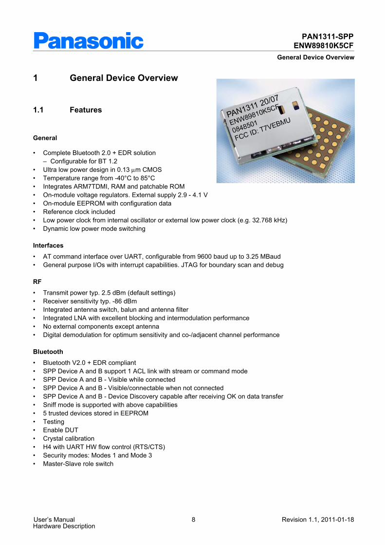
PAN1311-SPPENW89810K5CF
General Device Overview
1 General Device Overview
1.1 Features
General
• Complete Bluetooth 2.0 + EDR solution– Configurable for BT 1.2
• Ultra low power design in 0.13 μm CMOS• Temperature range from -40°C to 85°C• Integrates ARM7TDMI, RAM and patchable ROM• On-module voltage regulators. External supply 2.9 - 4.1 V• On-module EEPROM with configuration data• Reference clock included• Low power clock from internal oscillator or external low power clock (e.g. 32.768 kHz)• Dynamic low power mode switching
Interfaces• AT command interface over UART, configurable from 9600 baud up to 3.25 MBaud• General purpose I/Os with interrupt capabilities. JTAG for boundary scan and debug
RF• Transmit power typ. 2.5 dBm (default settings)• Receiver sensitivity typ. -86 dBm• Integrated antenna switch, balun and antenna filter• Integrated LNA with excellent blocking and intermodulation performance• No external components except antenna• Digital demodulation for optimum sensitivity and co-/adjacent channel performance
Bluetooth• Bluetooth V2.0 + EDR compliant• SPP Device A and B support 1 ACL link with stream or command mode• SPP Device A and B - Visible while connected• SPP Device A and B - Visible/connectable when not connected• SPP Device A and B - Device Discovery capable after receiving OK on data transfer• Sniff mode is supported with above capabilities• 5 trusted devices stored in EEPROM• Testing• Enable DUT• Crystal calibration• H4 with UART HW flow control (RTS/CTS)• Security modes: Modes 1 and Mode 3• Master-Slave role switch
User’s Manual 8 Revision 1.1, 2011-01-18Hardware Description
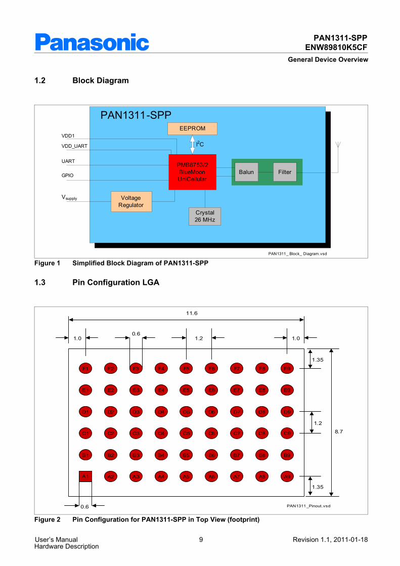
PAN1311-SPPENW89810K5CF
General Device Overview
1.2 Block Diagram
PAN1311_ Block_ Diagram.vsd
PAN1311-SPP
PMB8753/2BlueMoon UniCellular
EEPROM
Voltage Regulator
Crystal26 MHz
Balun Filter
I2C
Vsupply
GPIO
UART
VDD_UART
VDD1
Figure 1 Simplified Block Diagram of PAN1311-SPP
1.3 Pin Configuration LGA
PAN1311_Pinout.vsd0.6
A2 A3 A4 A5 A6 A7 A8 A9
B1 B2 B3 B4 B5 B6 B7 B8 B9
C1 C2 C3 C4 C5 C6 C7 C8 C9
D1 D2 D3 D4 D5 D6 D7 D8 D9
E1 E2 E3 E4 E5 E6 E7 E8 E9
F1 F2 F3 F4 F5 F6 F7 F8 F9
A1
1.2 1.01.00.6
1.2
1.35
1.35
11.6
8.7
Figure 2 Pin Configuration for PAN1311-SPP in Top View (footprint)
User’s Manual 9 Revision 1.1, 2011-01-18Hardware Description

PAN1311-SPPENW89810K5CF
General Device Overview
1.4 Pin DescriptionThe non-shaded cells indicate pins that will be fixed for the product lifetime. Shaded cells indicate that the pin might be removed/changed in future variants. Pins not listed below shall not be connected.
Table 1 Pin DescriptionPin No.
Symbol Input / Output
Supply Voltage During Reset
After Reset
Function
A2 P1.6 I/O/OD Internal1 Z Z Port 1.6A3 RESET# AI Internal1 Input Input Hardware ResetA8 P1.5 I/O/OD Internal1 Input Input Port 1.5B1 P1.7 I/O/OD Internal1 PD/ Input PD/ Input Port 1.7B2 P1.8 I/O/OD Internal1 PD PD Port 1.8B3 P1.0 /
TMSI/O/OD Internal2 PU1) PU1) Port 1.0 or
JTAG interfaceB4 P1.4 /
RTCKI/O/OD Internal2 Z Z Port 1.4 or
JTAG interfaceB5 ONOFF I - - Turns off module completelyB9 SLEEPX I/O VDDUART PD H Sleep indication signalC2 P0.9 I/O/OD Internal2 Z Z Port 0.9C3 JTAG# I Internal2 PU PU Mode selection Port 1:
0: JTAG1: Port
C4 TRST# I Internal2 PD PD JTAG interfaceD1 P0.10 I/O/OD Internal2 Z Z Port 0.10D2 P0.8 I/O/OD Internal2 PD PD Port 0.8D3 P1.1 /
TCKI/O/OD Internal2 PU1) PU1) Port 1.1 or
JTAG interfaceD4 P0.3 I/O/OD VDD1 Conf.
PD def.Conf. PD def.
Port 0.3
D5 P0.2 I/O/OD VDD1 Z Z Port 0.2D9 ANTENNA AI/AO Inactive Inactive RF input/output single endedE1 P0.12 / SDA0 I/O/OD Internal2 PU PU I2C data signalE2 P0.13 / SCL0 I/O/OD Internal2 PU PU I2C clock signalE3 P1.3 /
TDOI/O/OD Internal2 Z Z Port 1.3 or
JTAG interfaceE4 P0.0 I/O/OD VDD1 PD PD Port 0.0
LPM wakeup outputE5 P0.1 I/O/OD VDD1 PD PD Port 0.1E6 P0.5 /
UARTRXDI/O/OD VDDUART Z Z Port 0.5 or
UART receive dataF2 P1.2 /
TDII/O/OD Internal2 PU1) PU1) Port 1.2 or
JTAG interfaceF3 P0.11 I/O/OD Internal2 Z Z Port 0.11
User’s Manual 10 Revision 1.1, 2011-01-18Hardware Description

PAN1311-SPPENW89810K5CF
General Device Overview
Descriptions of acronyms used in the pin list:
InputOutputOutput with open drain capabilityTristatePull-upPull-downAnalog (e.g. AI means analog input)Supply (e.g. SO means supply output)
F4 P0.14 I/O VDDUART Z Z Port 0.14 LPM wakup input
F5 P0.7 / UARTCTS
I/O/OD VDDUART Z Z Port 0.7 orUART CTS flow control
F7 P0.4 / UARTTXD
I/O/OD VDDUART PU PU Port 0.4 orUART transmit data
F8 P0.6 / UARTRTS
I/O/OD VDDUART PU PU Port 0.6 orUART RTS flow control
A4, A5, A6
VSUPPLY SI - - Power supply
C1 VREG SO - - Regulated Power supplyF6 VDDUART SI - - UART interface Power supplyC5 VDD1 SI - - Power supplyA1, A7, A9, C8, C9, D7, D8, E8, E9, F1, F9
VSS - - Ground
1) Fixed pull-up/pull-down if JTAG interface is selected, not affected by any chip reset. If JTAG interface is not selected the port is tristate.
Acronym DescriptionIOODZPUPDAS
Table 1 Pin DescriptionPin No.
Symbol Input / Output
Supply Voltage During Reset
After Reset
Function
User’s Manual 11 Revision 1.1, 2011-01-18Hardware Description

PAN1311-SPPENW89810K5CF
General Device Overview
1.5 System IntegrationPAN1311-SPP is optimized for a low bill of material (BOM) and a small PCB size. Figure 3 shows a typical application example.
Example_Application_PAN1311.vsd
BT Baseband
BT Stack
RFCOMM
API
BT RF
Oscillator
HOST
I2C
BALUN
RESET
Antenna
Loaded from EEPROM
SPP(Serial Port Profile)
AT interface
UART
command
Keys,Leds
EEPROM
Voltage
Regulator
VSUPPLY
GPIO
Figure 3 Example of a Bluetooth System using eUniStone
User’s Manual 12 Revision 1.1, 2011-01-18Hardware Description
PAN1311-SPPENW89810K5CF
General Device Overview
The UART interface is used for communication between the host and PAN1311-SPP. The lines UARTTXD and UARTRXD are used for commands, events and data. The lines UARTRTS and UARTCTS are used for hardware flow control.Low power mode control of PAN1311-SPP and the host can be implemented in by using the pins P0.14 and P0.0. P0.14 is used by the host to allow PAN1311-SPP to enter low power mode and P0.0 is used by PAN1311-SPP to wake-up the host when attention is required. Additionally, the host could hardware reset PAN1311-SPP using the RESET# pin.Power is supplied to a single VSUPPLY input from which internal regulators can generate all required voltages. The UART and the GPIO’s interfaces have separate supply voltages so that they can comply with host signaling.
1.6 FW versionPAN1311-SPP is available in different versions. Please check corresponding release documents for latest information.
User’s Manual 13 Revision 1.1, 2011-01-18Hardware Description
PAN1311-SPPENW89810K5CF
User’s Manual 14 Revision 1.1, 2011-01-18Hardware Description
Basic Operating Information
2 Basic Operating Information
2.1 Power SupplyPAN1311-SPP is supplied from a single supply voltage VSUPPLY. This supply voltage must always be present. The PAN1311-SPP chip is supplied from an internally generated 2.5 V supply voltage. This voltage can be accessed from the VREG pin. This voltage may not be used for supplying other components in the host system but can be used for referencing the host interfaces.The GPIO’s and the UART interface are supplied with dedicated, independent, reference levels via the VDD1 and VDDUART pins. All other digital I/O pins are supplied internally by either 2.5 V (Internal2) or 1.5 V (Internal1). Section 1.4 provides a mapping between pins and supply voltages.The I/O power domains (VDD1 and VDDUART) are completely separated from the other power domains and can stay present also in low power modes.
2.2 ClockingPAN1311-SPP contains a crystal from which the internal 26 MHz system clock is generated. Also, the low power mode clock of 32 kHz is generated internally, which means that no external clock is needed.

PAN1311-SPPENW89810K5CF
User’s Manual 15 Revision 1.1, 2011-01-18Hardware Description
Interfaces
3 Interfaces
3.1 UART InterfaceThe UART interface is the main communication interface between the host and PAN1311-SPP. The interface consists of four UART signals and two wake-up signals as shown in Figure 4.
UARTTXDUARTRXDUARTRTSUARTCTS
WAKEUP_BTWAKEUP_HOST
UARTTXDUARTRXDUARTRTSUARTCTS
P0.14 inputP0.0 output
Host PAN1311
Figure 4 UART Interface
3.1.1 UARTThe UART (Universal Asynchronous Receiver and Transmitter) interface is compatible with standard UART H4 (4-wire). The lines UARTTXD and UARTRXD are used for commands, events and data. The lines UARTRTS and UARTCTS are used for hardware flow control. A separate supply voltage, VDDUART, makes it easy to connect the UART interface to any system.
3.1.1.1 Baud RatesThe supported baud rates are listed in Table 2 together with the small deviation error that results from the internal clock generation. The default baud rate is 115200 Baud.
9615 0.1619230 0.1638461 0.1657522 -0.14115044 -0.14230088 -0.14464285 0.76928571 0.761857142 0.763250000 0
Table 2 UART Baud Rates Wanted Baud Rate Real Baud Rate Deviation Error (%)960019200384005760011520023040046080092160018432003250000

PAN1311-SPPENW89810K5CF
User’s Manual 16 Revision 1.1, 2011-01-18Hardware Description
General Device Capabilities
4 General Device CapabilitiesThis chapter describes features available in the PAN1311 (ENW89810K5CF 20/xx) core.Actual feature set and how to access the features can be found in the AT Command document [1]. Release specific performance characteristics, like data speed, is related in the SW Release Notes [2].
4.1 HCI+The PAN1311 module can be programmed over UART with a specific application for RF test purposes, like TX continuous or TX burst mode. This test application is controlled over the UART through Infineon specific HCI commands. The commands supported by this test application are described in the document “T8753-2-Infineon_Specific_HCI_Commands-7600.pdf”.
4.2 Firmware ROM Patching
4.2.1 Patch SupportPAN1311-SPP contains dedicated hardware that makes it possible to apply patches to the code and data in the firmware ROM. The hardware is capable of replacing up to 32 blocks of 16 bytes each with new content. This area can be filled with any combination of code and data. The firmware patch is stored in EEPROM and automatically loaded after startup. This provides a flexible bugfix solution for the ROM part of the firmware.
PAN1311-SPPENW89810K5CF
Bluetooth Capabilities
5 Bluetooth Capabilities
5.1 Supported Features
• Bluetooth V2.0 + EDR compliant• Enhanced Data Rate up to 3 Mbit/s• Adaptive Frequency Hopping (AFH)• All packet types• Authentication, Pairing and Encryption• SPP Device A and B support 1 ACL link with stream or command mode• SPP Device A and B - Visible while connected• SPP Device A and B - Visible/connectable when not connected• SPP Device A and B - Device Discovery capable after receiving OK on data transfer• Sniff mode is supported with above capabilities• 5 trusted devices stored in EEPROM• Enable DUT• Crystal calibration• H4 with UART HW flow control (RTS/CTS)• Security modes: Modes 1 and Mode 3• Master-Slave role switch• Quality of Service• Channel Quality Driven Data Rate change• Sniff, Hold• Role Switch• RSSI and Power Control• Power class 2 and 3• Standard Bluetooth test mode, Active Tester Mode and RF Test Modes
User’s Manual 17 Revision 1.1, 2011-01-18Hardware Description

PAN1311-SPPENW89810K5CF
Bluetooth Capabilities
5.2 PAN1311-SPP Specifics and Extensions
5.2.1 During Connection
5.2.1.1 Role SwitchOnly one role switch can be performed at a time. If a role switch request is pending, other role switch requests on the same or other links are rejected. If a role switch fails, PAN1311-SPP will automatically try again a maximum of three times. Encryption (if present) is stopped in the old piconet before a role switch is performed and re-enabled when the role switch has succeeded or failed.
5.2.1.2 Dynamic Polling StrategyIn addition to the regular polling scheme, PAN1311-SPP dynamically assigns unused slots to links where data is exchanged. This adapts very well to bursty traffic and improves throughput and latency on the links.
5.2.1.3 Adaptive Frequency Hopping (AFH)PAN1311-SPP supports adaptive frequency hopping according to the Bluetooth 2.0 + EDR specification. AFH switch and channel classification are supported both as master and slave. Channel classification from the host is also supported.A number of HCI+ commands and events are available to provide information about AFH operation. The commands Infineon_Enable_AFH_Info_Sending and Infineon_Disable_AFH_Info_Sending turn on and off the Infineon AFH Info events that provide detailed information about channel classification, channel maps, interferers, etc.If enabled by the Infineon_Enable_Infineon_Events command, the Infineon AFH Extraordinary RSSI event informs the host whenever extraordinary RSSI measurements in unused slots have been started. This is done when the number of known good channels has decreased below a critical limit and periodically after a defined time.The Infineon_Set_AFH_Measurement_Period command can be used to configure the duration of the AFH measurement period.
5.2.1.4 Channel Quality Driven Data Rate Change (CQDDR)PAN1311-SPP supports channel quality driven data rate change according to the Bluetooth 2.0 + EDR specification. A device that receives an LMP_preferred_rate message is not required to follow all recommendations. PAN1311-SPP normally at least follows the recommendation whether to use forward error correction (FEC) or not. If possible, recommendations about packet size and modulation scheme will be taken into account. When PAN1311-SPP sends an LMP_preferred_rate to another device the proposal always includes preferences for all parameters.The HCI+ commands Infineon_Enable_CQDDR_Info_Sending and Infineon_Disable_CQDDR_Info_Sending turn on and off sending of the Infineon CQDDR Info event. This event provides information to the host every time a new CQDDR proposal is sent to a remote device.
User’s Manual 18 Revision 1.1, 2011-01-18Hardware Description
PAN1311-SPPENW89810K5CF
Bluetooth Capabilities
5.2.2 RSSI and Output Power Control
5.2.2.1 Received Signal Strength Indication (RSSI)PAN1311-SPP supports received signal strength measurements and uses LMP signaling to keep the output power of a remote device within the golden receive power range. The range is set with the BD_DATA parameters RSSI_Min and RSSI_Max.
5.2.2.2 Output Power ControlPAN1311-SPP supports power control according to the Bluetooth 2.0+EDR specification.• The output power can be controlled in up to 4 configurable steps. PAN1311-SPP can work as a class 2 or 3
device, depending on the settings.• Fine tuning can be used on the power steps.• A default sub-state power step can be setThe power step configuration is set through BD_DATA parameters.The Inquiry output power can be programmed with the Write Inquiry Transmit Power Level command introduced in the 2.0 Bluetooth Core specification.
5.2.2.3 Ultra Low Transmit PowerFor high security devices the output power can be reduced to a value that reduces the communication range to a few inches. This mode is enabled with the HCI+ command Infineon_TX_Power_Config.
User’s Manual 19 Revision 1.1, 2011-01-18Hardware Description
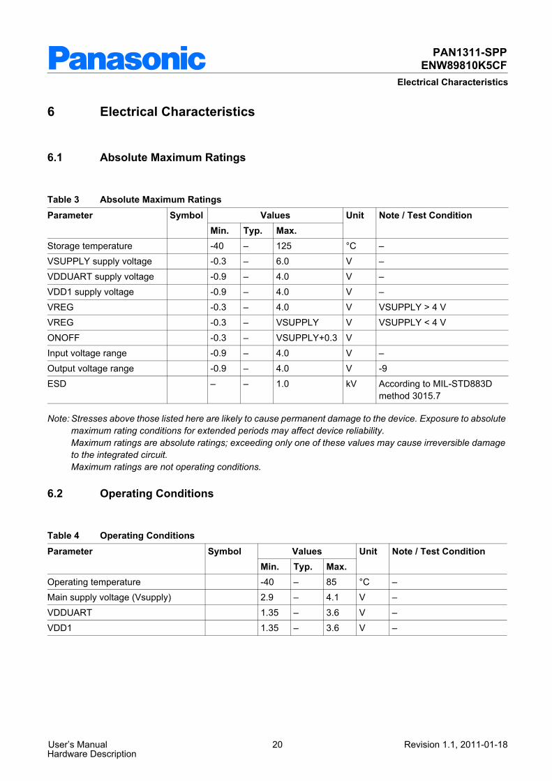
PAN1311-SPPENW89810K5CF
Electrical Characteristics
6 Electrical Characteristics
6.1 Absolute Maximum Ratings
Values
-40 – 125 °C –-0.3 – 6.0 V –-0.9 – 4.0 V –-0.9 – 4.0 V –-0.3 – 4.0 V VSUPPLY > 4 V-0.3 – VSUPPLY V VSUPPLY < 4 V-0.3 – VSUPPLY+0.3 V-0.9 – 4.0 V –-0.9 – 4.0 V -9– – 1.0 kV According to MIL-STD883D
method 3015.7
Note: Stresses above those listed here are likely to cause permanent damage to the device. Exposure to absolute maximum rating conditions for extended periods may affect device reliability. Maximum ratings are absolute ratings; exceeding only one of these values may cause irreversible damage to the integrated circuit. Maximum ratings are not operating conditions.
6.2 Operating Conditions
Values
-40 – 85 °C –2.9 – 4.1 V –1.35 – 3.6 V –1.35 – 3.6 V –
Table 3 Absolute Maximum Ratings Parameter Symbol Unit Note / Test Condition
Min. Typ. Max.Storage temperatureVSUPPLY supply voltageVDDUART supply voltageVDD1 supply voltageVREGVREGONOFFInput voltage rangeOutput voltage rangeESD
Table 4 Operating Conditions Parameter Symbol Unit Note / Test Condition
Min. Typ. Max.Operating temperatureMain supply voltage (Vsupply)VDDUARTVDD1
User’s Manual 20 Revision 1.1, 2011-01-18Hardware Description
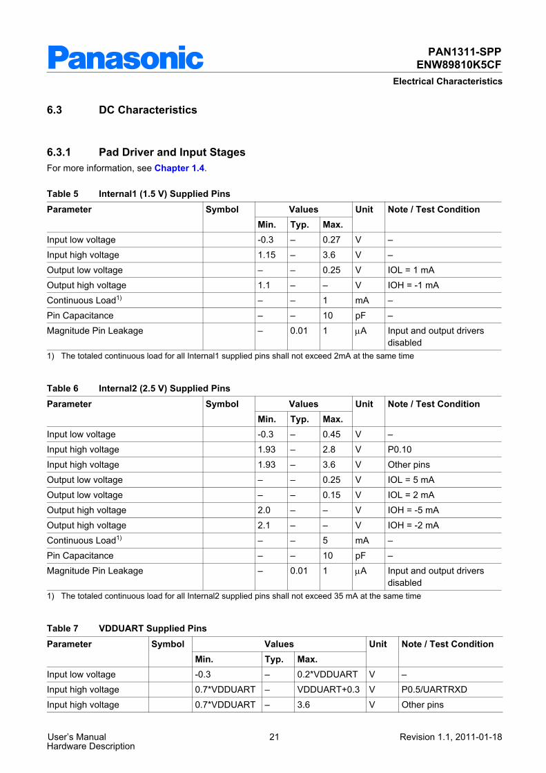
PAN1311-SPPENW89810K5CF
Electrical Characteristics
6.3 DC Characteristics
6.3.1 Pad Driver and Input StagesFor more information, see Chapter 1.4.
Values
-0.3 – 0.27 V –1.15 – 3.6 V –– – 0.25 V IOL = 1 mA1.1 – – V IOH = -1 mA– – 1 mA –– – 10 pF –– 0.01 1 μA Input and output drivers
disabled
Values
-0.3 – 0.45 V –1.93 – 2.8 V P0.101.93 – 3.6 V Other pins– – 0.25 V IOL = 5 mA– – 0.15 V IOL = 2 mA2.0 – – V IOH = -5 mA2.1 – – V IOH = -2 mA– – 5 mA –– – 10 pF –– 0.01 1 μA Input and output drivers
disabled
Table 5 Internal1 (1.5 V) Supplied Pins Parameter Symbol Unit Note / Test Condition
Min. Typ. Max.Input low voltageInput high voltageOutput low voltageOutput high voltageContinuous Load1)
1) The totaled continuous load for all Internal1 supplied pins shall not exceed 2mA at the same time
Pin CapacitanceMagnitude Pin Leakage
Table 6 Internal2 (2.5 V) Supplied Pins Parameter Symbol Unit Note / Test Condition
Min. Typ. Max.Input low voltageInput high voltageInput high voltageOutput low voltageOutput low voltageOutput high voltageOutput high voltageContinuous Load1)
1) The totaled continuous load for all Internal2 supplied pins shall not exceed 35 mA at the same time
Pin CapacitanceMagnitude Pin Leakage
Table 7 VDDUART Supplied Pins Parameter Symbol Values Unit Note / Test Condition
Min. Typ. Max.Input low voltage -0.3 – 0.2*VDDUART V –Input high voltage 0.7*VDDUART – VDDUART+0.3 V P0.5/UARTRXDInput high voltage 0.7*VDDUART – 3.6 V Other pins
User’s Manual 21 Revision 1.1, 2011-01-18Hardware Description
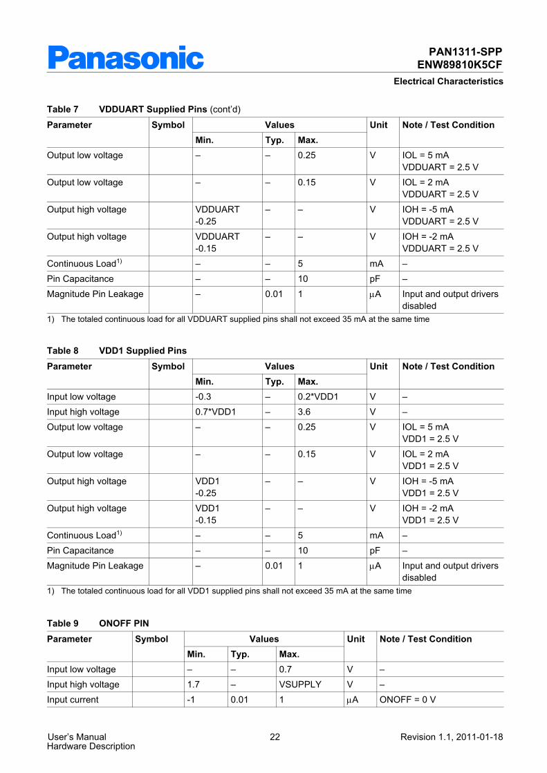
PAN1311-SPPENW89810K5CF
Electrical Characteristics
Output low voltage – – 0.25 V IOL = 5 mA VDDUART = 2.5 V
Output low voltage – – 0.15 V IOL = 2 mA VDDUART = 2.5 V
Output high voltage VDDUART -0.25
– – V IOH = -5 mA VDDUART = 2.5 V
Output high voltage VDDUART -0.15
– – V IOH = -2 mA VDDUART = 2.5 V
Continuous Load1) – – 5 mA –Pin Capacitance – – 10 pF –Magnitude Pin Leakage – 0.01 1 μA Input and output drivers
disabled
Values
-0.3 – 0.2*VDD1 V –0.7*VDD1 – 3.6 V –– – 0.25 V IOL = 5 mA
VDD1 = 2.5 V– – 0.15 V IOL = 2 mA
VDD1 = 2.5 VVDD1 -0.25
– – V IOH = -5 mA VDD1 = 2.5 V
VDD1 -0.15
– – V IOH = -2 mA VDD1 = 2.5 V
– – 5 mA –– – 10 pF –– 0.01 1 μA Input and output drivers
disabled
Values
– – 0.7 V –1.7 – VSUPPLY V –-1 0.01 1 μA ONOFF = 0 V
1) The totaled continuous load for all VDDUART supplied pins shall not exceed 35 mA at the same time
Table 8 VDD1 Supplied Pins Parameter Symbol Unit Note / Test Condition
Min. Typ. Max.Input low voltageInput high voltageOutput low voltage
Output low voltage
Output high voltage
Output high voltage
Continuous Load1)
1) The totaled continuous load for all VDD1 supplied pins shall not exceed 35 mA at the same time
Pin CapacitanceMagnitude Pin Leakage
Table 9 ONOFF PIN Parameter Symbol Unit Note / Test Condition
Min. Typ. Max.Input low voltageInput high voltageInput current
Table 7 VDDUART Supplied Pins (cont’d)
Parameter Symbol Values Unit Note / Test ConditionMin. Typ. Max.
User’s Manual 22 Revision 1.1, 2011-01-18Hardware Description
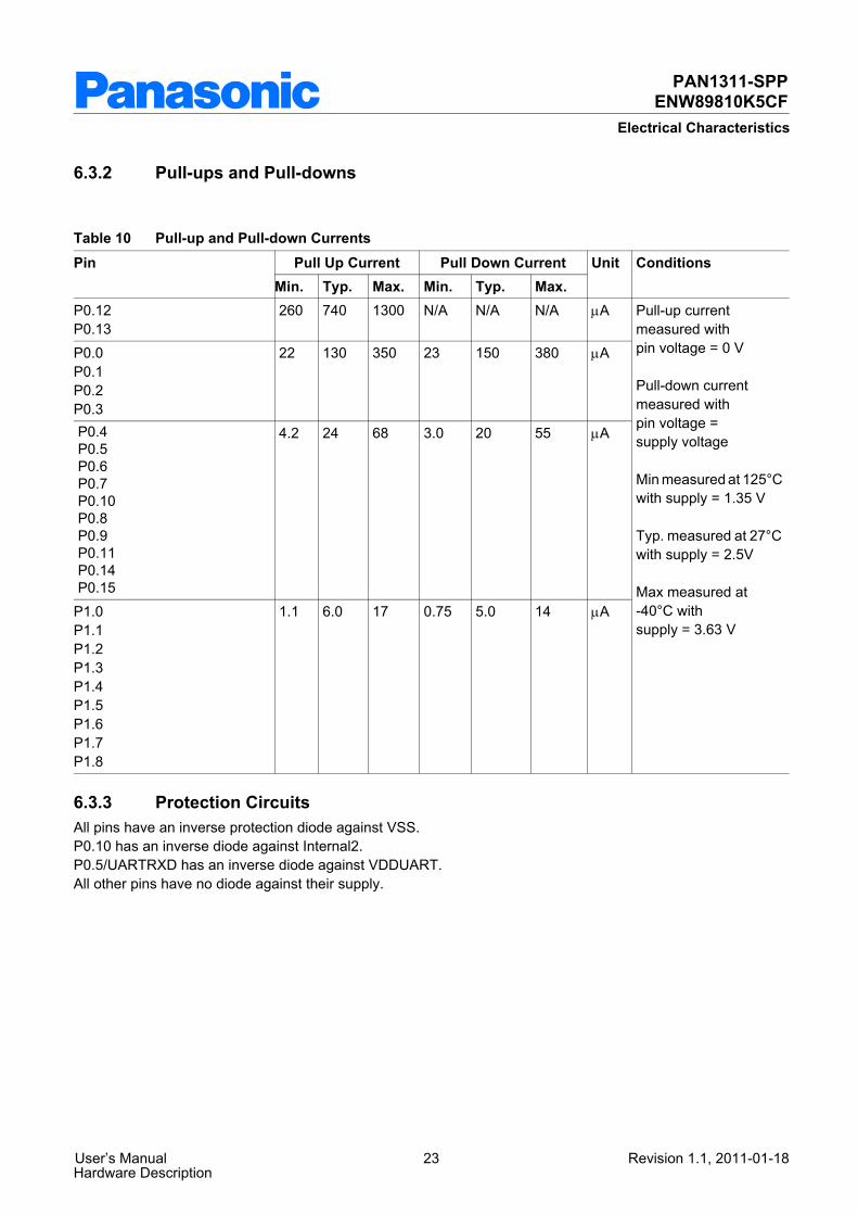
PAN1311-SPPENW89810K5CF
Electrical Characteristics
6.3.2 Pull-ups and Pull-downs
260 740 1300 N/A N/A N/A μA Pull-up current measured with pin voltage = 0 V
Pull-down current measured with pin voltage = supply voltage
Min measured at 125°C with supply = 1.35 V
Typ. measured at 27°C with supply = 2.5V
Max measured at -40°C with supply = 3.63 V
22 130 350 23 150 380 μA
4.2 24 68 3.0 20 55 μA
1.1 6.0 17 0.75 5.0 14 μA
6.3.3 Protection CircuitsAll pins have an inverse protection diode against VSS. P0.10 has an inverse diode against Internal2. P0.5/UARTRXD has an inverse diode against VDDUART. All other pins have no diode against their supply.
Table 10 Pull-up and Pull-down Currents Pin Pull Up Current Pull Down Current Unit Conditions
Min. Typ. Max. Min. Typ. Max.P0.12 P0.13P0.0 P0.1 P0.2 P0.3P0.4 P0.5 P0.6 P0.7 P0.10 P0.8 P0.9 P0.11 P0.14 P0.15
P1.0 P1.1 P1.2 P1.3 P1.4 P1.5 P1.6 P1.7 P1.8
User’s Manual 23 Revision 1.1, 2011-01-18Hardware Description
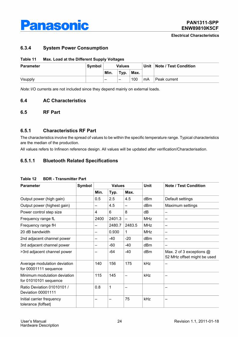
PAN1311-SPPENW89810K5CF
Electrical Characteristics
6.3.4 System Power Consumption
Values
– – 100 mA Peak current
Note: I/O currents are not included since they depend mainly on external loads.
6.4 AC Characteristics
6.5 RF Part
6.5.1 Characteristics RF PartThe characteristics involve the spread of values to be within the specific temperature range. Typical characteristics are the median of the production.All values refers to Infineon reference design. All values will be updated after verification/Characterisation.
6.5.1.1 Bluetooth Related Specifications
Table 11 Max. Load at the Different Supply Voltages Parameter Symbol Unit Note / Test Condition
Min. Typ. Max.Vsupply
Table 12 BDR - Transmitter Part Parameter Symbol Values Unit Note / Test Condition
Min. Typ. Max.Output power (high gain) 0.5 2.5 4.5 dBm Default settingsOutput power (highest gain) – 4.5 – dBm Maximum settingsPower control step size 4 6 8 dB –Frequency range fL 2400 2401.3 – MHz –Frequency range fH – 2480.7 2483.5 MHz –20 dB bandwidth – 0.930 1 MHz –2nd adjacent channel power – -40 -20 dBm –3rd adjacent channel power – -60 -40 dBm –>3rd adjacent channel power – -64 -40 dBm Max. 2 of 3 exceptions @
52 MHz offset might be usedAverage modulation deviation for 00001111 sequence
140 156 175 kHz –
Minimum modulation deviation for 01010101 sequence
115 145 – kHz –
Ratio Deviation 01010101 / Deviation 00001111
0.8 1 – –
Initial carrier frequency tolerance |foffset|
– – 75 kHz –
User’s Manual 24 Revision 1.1, 2011-01-18Hardware Description
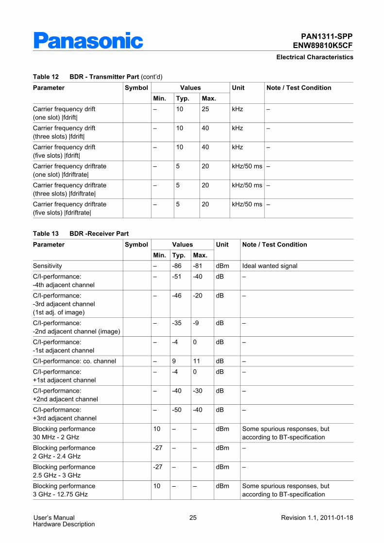
PAN1311-SPPENW89810K5CF
Electrical Characteristics
Carrier frequency drift (one slot) |fdrift|
– 10 25 kHz –
Carrier frequency drift (three slots) |fdrift|
– 10 40 kHz –
Carrier frequency drift (five slots) |fdrift|
– 10 40 kHz –
Carrier frequency driftrate (one slot) |fdriftrate|
– 5 20 kHz/50 ms –
Carrier frequency driftrate (three slots) |fdriftrate|
– 5 20 kHz/50 ms –
Carrier frequency driftrate (five slots) |fdriftrate|
– 5 20 kHz/50 ms –
Table 13 BDR -Receiver Part Parameter Symbol Values Unit Note / Test Condition
Min. Typ. Max.Sensitivity – -86 -81 dBm Ideal wanted signalC/I-performance: -4th adjacent channel
– -51 -40 dB –
C/I-performance: -3rd adjacent channel (1st adj. of image)
– -46 -20 dB –
C/I-performance: -2nd adjacent channel (image)
– -35 -9 dB –
C/I-performance: -1st adjacent channel
– -4 0 dB –
C/I-performance: co. channel – 9 11 dB –C/I-performance: +1st adjacent channel
– -4 0 dB –
C/I-performance: +2nd adjacent channel
– -40 -30 dB –
C/I-performance: +3rd adjacent channel
– -50 -40 dB –
Blocking performance 30 MHz - 2 GHz
10 – – dBm Some spurious responses, but according to BT-specification
Blocking performance 2 GHz - 2.4 GHz
-27 – – dBm –
Blocking performance 2.5 GHz - 3 GHz
-27 – – dBm –
Blocking performance 3 GHz - 12.75 GHz
10 – – dBm Some spurious responses, but according to BT-specification
Table 12 BDR - Transmitter Part (cont’d)
Parameter Symbol Values Unit Note / Test ConditionMin. Typ. Max.
User’s Manual 25 Revision 1.1, 2011-01-18Hardware Description
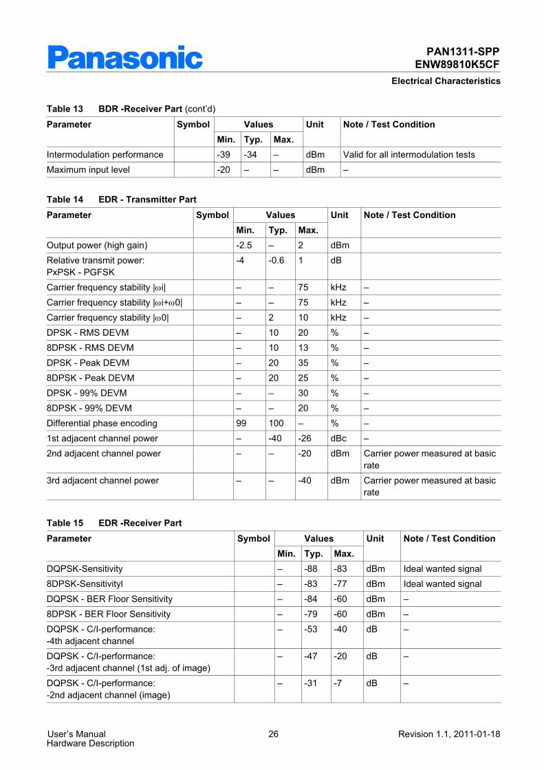
PAN1311-SPPENW89810K5CF
Electrical Characteristics
Intermodulation performance -39 -34 – dBm Valid for all intermodulation testsMaximum input level -20 – – dBm –
Values
-2.5 – 2 dBm-4 -0.6 1 dB
– – 75 kHz –– – 75 kHz –– 2 10 kHz –– 10 20 % –– 10 13 % –– 20 35 % –– 20 25 % –– – 30 % –– – 20 % –99 100 – % –– -40 -26 dBc –– – -20 dBm Carrier power measured at basic
rate– – -40 dBm Carrier power measured at basic
rate
Table 14 EDR - Transmitter Part Parameter Symbol Unit Note / Test Condition
Min. Typ. Max.Output power (high gain)Relative transmit power: PxPSK - PGFSKCarrier frequency stability |ωi|Carrier frequency stability |ωi+ω0|Carrier frequency stability |ω0|DPSK - RMS DEVM8DPSK - RMS DEVMDPSK - Peak DEVM8DPSK - Peak DEVMDPSK - 99% DEVM8DPSK - 99% DEVMDifferential phase encoding1st adjacent channel power2nd adjacent channel power
3rd adjacent channel power
Table 15 EDR -Receiver Part Parameter Symbol Values Unit Note / Test Condition
Min. Typ. Max.DQPSK-Sensitivity – -88 -83 dBm Ideal wanted signal8DPSK-Sensitivityl – -83 -77 dBm Ideal wanted signalDQPSK - BER Floor Sensitivity – -84 -60 dBm –8DPSK - BER Floor Sensitivity – -79 -60 dBm –DQPSK - C/I-performance: -4th adjacent channel
– -53 -40 dB –
DQPSK - C/I-performance: -3rd adjacent channel (1st adj. of image)
– -47 -20 dB –
DQPSK - C/I-performance: -2nd adjacent channel (image)
– -31 -7 dB –
Table 13 BDR -Receiver Part (cont’d)
Parameter Symbol Values Unit Note / Test ConditionMin. Typ. Max.
User’s Manual 26 Revision 1.1, 2011-01-18Hardware Description
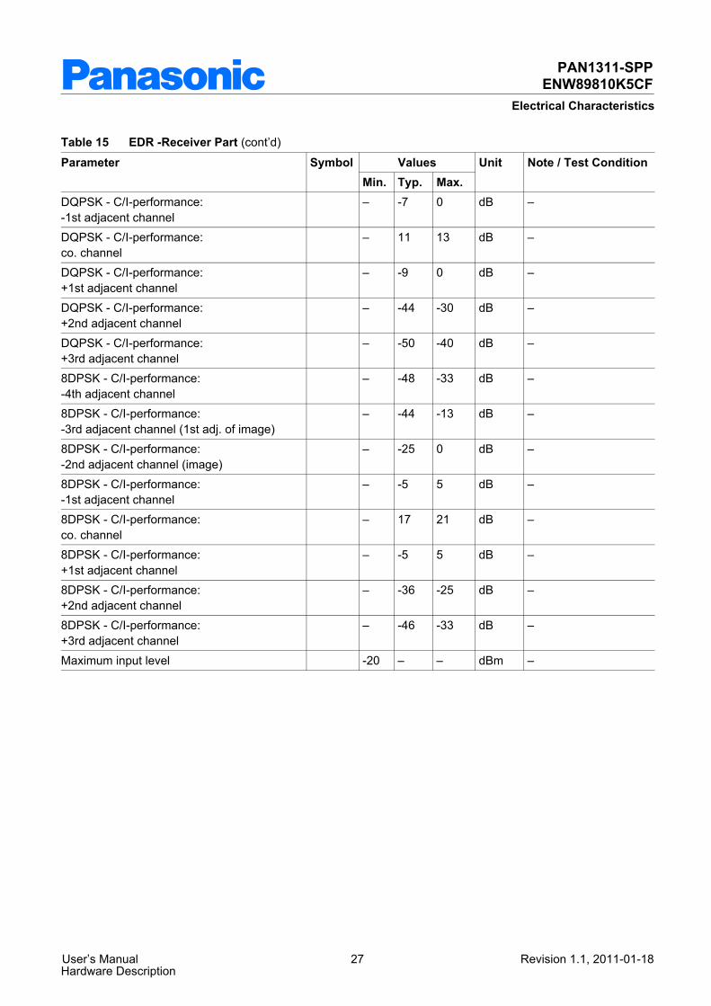
PAN1311-SPPENW89810K5CF
Electrical Characteristics
DQPSK - C/I-performance: -1st adjacent channel
– -7 0 dB –
DQPSK - C/I-performance: co. channel
– 11 13 dB –
DQPSK - C/I-performance: +1st adjacent channel
– -9 0 dB –
DQPSK - C/I-performance: +2nd adjacent channel
– -44 -30 dB –
DQPSK - C/I-performance: +3rd adjacent channel
– -50 -40 dB –
8DPSK - C/I-performance: -4th adjacent channel
– -48 -33 dB –
8DPSK - C/I-performance: -3rd adjacent channel (1st adj. of image)
– -44 -13 dB –
8DPSK - C/I-performance: -2nd adjacent channel (image)
– -25 0 dB –
8DPSK - C/I-performance: -1st adjacent channel
– -5 5 dB –
8DPSK - C/I-performance: co. channel
– 17 21 dB –
8DPSK - C/I-performance: +1st adjacent channel
– -5 5 dB –
8DPSK - C/I-performance: +2nd adjacent channel
– -36 -25 dB –
8DPSK - C/I-performance: +3rd adjacent channel
– -46 -33 dB –
Maximum input level -20 – – dBm –
Table 15 EDR -Receiver Part (cont’d)
Parameter Symbol Values Unit Note / Test ConditionMin. Typ. Max.
User’s Manual 27 Revision 1.1, 2011-01-18Hardware Description
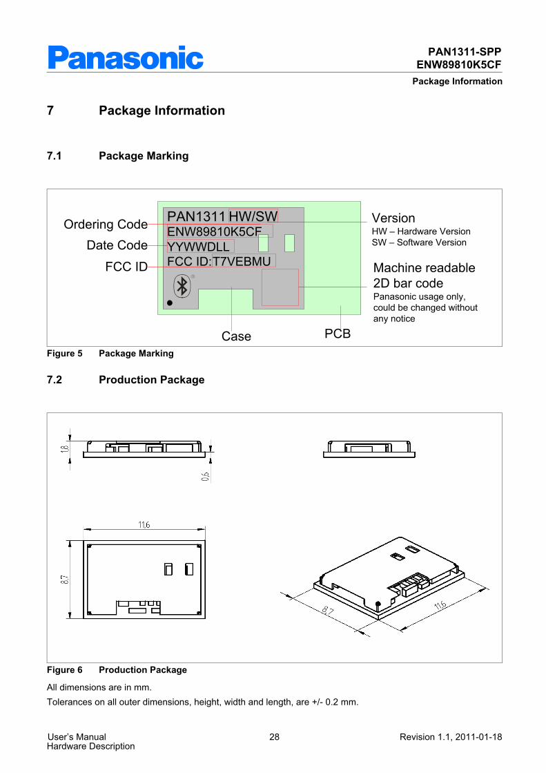
PAN1311-SPPENW89810K5CF
Package Information
7 Package Information
7.1 Package Marking
PAN1311ENW89810K5CFYYWWDLLFCC ID:T7VEBMU
VersionHW – Hardware VersionSW – Software Version
Ordering CodeDate Code
FCC ID Machine readable2D bar codePanasonic usage only, could be changed without any notice
Case PCB
HW/SW
Figure 5 Package Marking
7.2 Production Package
Figure 6 Production Package
All dimensions are in mm.Tolerances on all outer dimensions, height, width and length, are +/- 0.2 mm.
User’s Manual 28 Revision 1.1, 2011-01-18Hardware Description
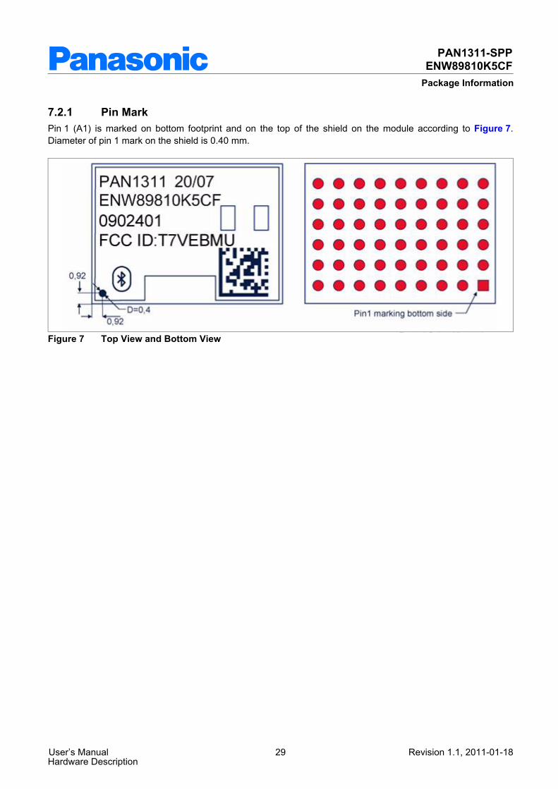
PAN1311-SPPENW89810K5CF
Package Information
7.2.1 Pin MarkPin 1 (A1) is marked on bottom footprint and on the top of the shield on the module according to Figure 7. Diameter of pin 1 mark on the shield is 0.40 mm.
Figure 7 Top View and Bottom View
User’s Manual 29 Revision 1.1, 2011-01-18Hardware Description
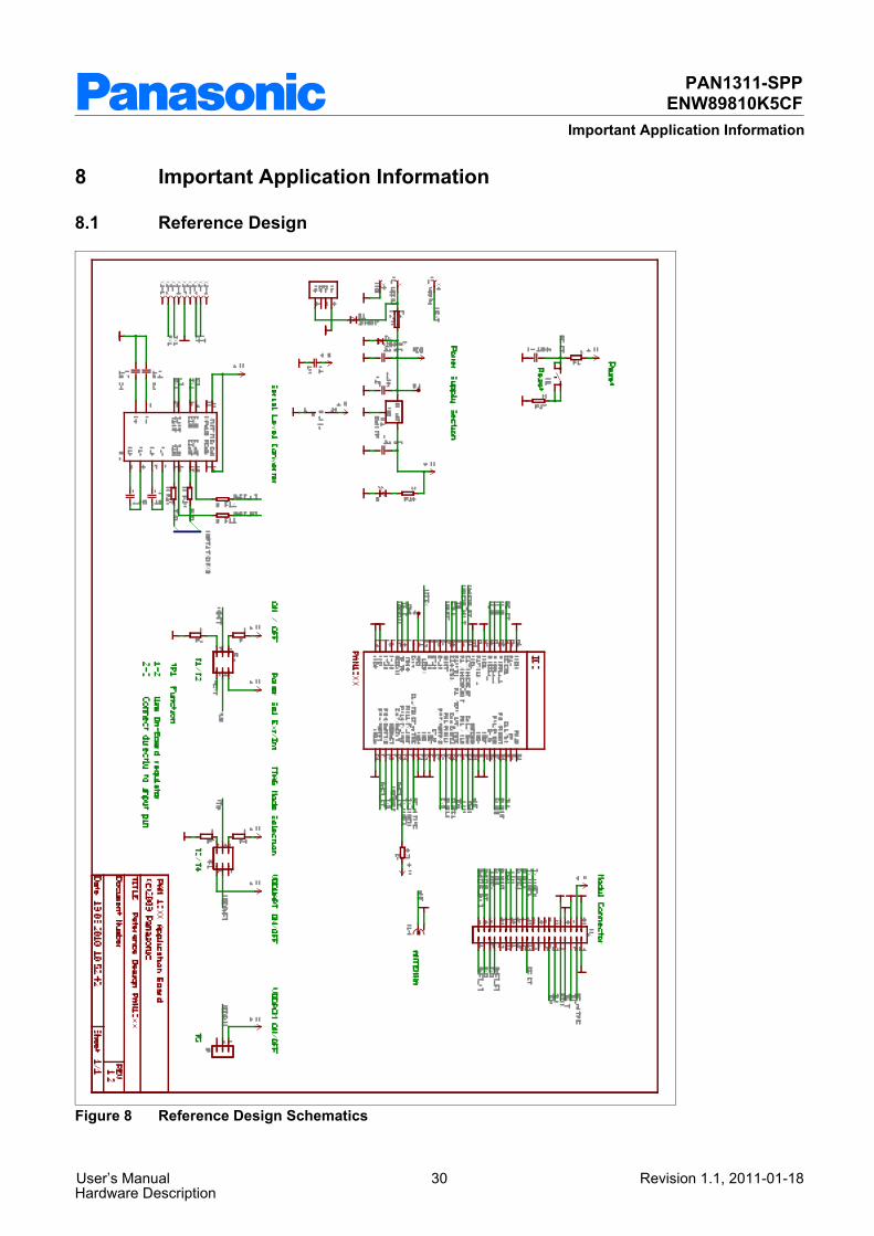
PAN1311-SPPENW89810K5CF
Important Application Information
8 Important Application Information
8.1 Reference Design
Figure 8 Reference Design Schematics
User’s Manual 30 Revision 1.1, 2011-01-18Hardware Description

PAN1311-SPPENW89810K5CF
Important Application Information
ENW89810K5CF 20/xx is intended to be installed inside end user equipment. ENW89810K5CF 20/xx is Bluetoooth-qualified and also FCC-certified and Industry Canada approved, and conforms to R&TTE (European) requirements and directives with the reference design described in Figure 8. FCC certification is valid together with the following antennas, having in mind, that this module has the Johansson antenna included:
Titanis Swivel 4 dBi 50 ohmP/N 1513151-1 Module 4 dBi 50 ohmLDA312G7313F-237 Ceramic chip 0 dBi 50 ohm
Printed inverted F Antenna (PIFA)
4 dBi 50 ohm
2450AT43A100 Ceramic chip antenna 2 dBi 50 ohmBST-2450 Dipole antenna 2 dBi 50 ohm
When using any of the above antennas, installed in the appropriate manner, it is possible to re-use the approvals for the end-product. It is, however, required to have a written consent from Infineon Technologies AG to re-use the regulatory approvals for the FCC, Canada and Europe.Manufacturers of mobile, fixed or portable devices incorporating this device are advised to clarify any regulatory questions and to have their complete product tested and approved for compliance (FCC or other when applicable). When using other antennas, a “class II permissive change” is required for FCC approval. The normal procedure is to first provide a technical test report showing that 4 dBi is not exceeded and to continue working with a regulatory test house to finalize the approval for a new antenna implementation.There are no parts in ENW89810K5CF 20/xx that can be modified by the user except modifications of the device BD data and loading of SW patches. Any changes or modifications made to this device that are not expressly approved by Infineon, may void the user’s authority to operate the equipment.
8.2 FCC Class B Digital Devices Regulatory NoticeThis equipment has been tested and found to comply with the limits for a Class B digital device, pursuant to Part 15 of the FCC Rules. These limits are designed to provide reasonable protection against harmful interference in a residential installation. This equipment generates, uses, and can radiate radio frequency energy and, if not installed and used in accordance with the instructions, may cause harmful interference to radio communications. However, there is no guarantee that interference will not occur in a particular installation. If this equipment does cause harmful interference to radio or television reception, which can be determined by turning the equipment off and on, the user is encouraged to try to correct the interference by 1 or more of the following measures:• Reorient or relocate the antenna• Increase the separation between the equipment and receiver• Connect the equipment into an outlet on a circuit different from that to which the receiver is connected• Consult the dealer or an experienced radio or television technician for help
8.3 FCC Wireless NoticeThis product emits radio frequency energy, but the radiated output power of this device is far below the FCC radio frequency exposure limits. Nevertheless, the device should be used in such a manner that the potential for human contact with the antenna during normal operation is minimized.To meet the FCC's RF exposure rules and regulations:• The system antenna used for this transmitter must not be co-located or operating in conjunction with any other
antenna or transmitter.
Table 16 AntennasManufacturer Model Type Peak antenna gain ImpedanceGigAntTyco ElectronicsMurataInfineon reference design
JohanssonInwave
User’s Manual 31 Revision 1.1, 2011-01-18Hardware Description
PAN1311-SPPENW89810K5CF
Important Application Information
• The system antenna used for this module must not exceed 4 dBi.• Users and installers must be provided with antenna installation instructions and transmitter operating
conditions for satisfying RF exposure compliance.Manufacturers of mobile, fixed or portable devices incorporating this module are advised to clarify any regulatory questions and to have their complete product tested and approved for FCC compliance.
8.4 FCC Interference StatementThis device complies with Part 15 of the FCC Rules. Operation is subject to the following two conditions:1. This device may not cause harmful interference2. This device must accept any interference received, including interference that may cause undesired operation.
8.5 FCC IdentifierFCC ID: T7VEBMU
8.6 European R&TTE Declaration of ConformityHereby, Panasonic Electronic Devices Europe GmbH, declares that the Bluetooth module ENW89810K5CF 20/xxis in compliance with the essential requirements and other relevant provisions of Directive 1999/5/EC.As a result of the conformity assessment procedure described in Annex III of the Directive 1999/5/EC, the end-customer equipment should be labelled as follows:
Figure 9 Equipment Label
PAN1311 in the specified reference design can be used in the following countries:Austria, Belgium, Cyprus, Czech Republic, Denmark, Estonia, Finland, France, Germany, Greece, Hungary, Ireland, Italy, Latvia, Lithuania, Luxembourg, Malta, Poland, Portugal, Slovakia, Slovenia, Spain, Sweden, The Netherlands, the United Kingdom, Switzerland, and Norway.
User’s Manual 32 Revision 1.1, 2011-01-18Hardware Description

PAN1311-SPPENW89810K5CF
Important Application Information
We, Panasonic Electronic Devices Europe GmbH
High Frequency Products Business Group
Zeppelinstrasse 19, 21337 Lueneburg, Germany
declare under our sole responsibility that the product:
Type of equipment: Bluetooth 2.0+EDR Module
Brand name: PAN1321 / PAN1311
Model name: ENW89811K4CF / ENW89810K5CF
to which this declaration relates, is in compliance with all the applicable essentialrequirements, and other provisions of the European Council Directive:
The conformity assessment procedure used for this declaration is Annex IV of this Directive.
Product compliance has been demonstrated on the basis of:
For article 3.1 (a) : Health and Safety of the User
For article 3.1 (b) : Electromagnetic Compatibility
The technical contruction file is kept available at:
Panasonic Electronic Devices Europe GmbH, Zeppelinstrasse 19, 21337 Lueneburg, Germany
Issued on: 31st of March 2010
Signed by the manufacturer:
(Company name) Panasonic Electronic Devices Europe GmbH
(Signature)
(Printed name) Heino Kaehler
(Title) Manager Wireless Modules
For article 3.2 : Effective use of spectrum allocated- EN 300 328 V1.6.1 (2004-11)- EN 300 328 V1.7.1 (2006-10)
- IEC 60950-1 (2006)
- EN 301 489-1 V1.8.1- EN 301 489-17 V2.1.1
Declaration of Conformity (DoC)1999/5/EC
1999/5/EC Radio and Telecommunications Terminal Equipment Directive (R&TTE)
Figure 10 Declaration of Conformity
User’s Manual 33 Revision 1.1, 2011-01-18Hardware Description

PAN1311-SPPENW89810K5CF
Important Application Information
8.7 Bluetooth Qualified Design IDPanasonic has submitted End Product Listing (EPL) for PAN1311, based on Infineon eBMU plattform, in the Qualified Product List of the Bluetooth SIG. These EPL are referring the Bluetooth qualfication of the SPP-AT application running on the eBMU chip under QD ID B014433.Manufacturers of Bluetooth devices incorporating PAN1311can reference the same QD ID number.Bluetooth QD ID: B014433 (PAN1311 SPP BT2.0).
8.8 Industry Canada CertificationPAN1311 complies with the regulatory requirements of Industry Canada (IC), license: IC: 216Q-EBMUManufacturers of mobile, fixed or portable devices incorporating this module are advised to clarify any regulatory questions and ensure compliance for SAR and/or RF exposure limits. Users can obtain Canadian information on RF exposure and compliance from www.ic.gc.ca.This device has been designed to operate with the antennas listed in Table 16 above, having a maximum gain of 4.0 dBi. Antennas not included in this list or having a gain greater than 4.0 dBi are strictly prohibited for use with this device. The required antenna impedance is 50 ohms. The antenna used for this transmitter must not be co-located or operating in conjunction with any other antenna or transmitter.
8.9 Label Design of the Host ProductIt is recommended to include the following information on the host product label:Contains transmitter Module FCC ID: T7VEBMU / IC: 216QEBMU
8.10 Regulatory Test HouseThe test house used by Panasonic in the Bluetooth and Regulatory approvals for the module PAN1311:Eurofins Product Service GmbHStorkower Str. 38cD-15526 Reichenwalde b. BerlinGERMANYTel.: +49 33631 888 0Fax: +49 33631 888 650www.eurofins.com
User’s Manual 34 Revision 1.1, 2011-01-18Hardware Description
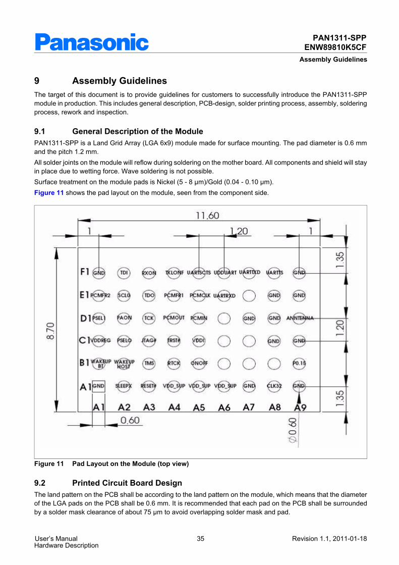
PAN1311-SPPENW89810K5CF
Assembly Guidelines
9 Assembly GuidelinesThe target of this document is to provide guidelines for customers to successfully introduce the PAN1311-SPPmodule in production. This includes general description, PCB-design, solder printing process, assembly, soldering process, rework and inspection.
9.1 General Description of the ModulePAN1311-SPP is a Land Grid Array (LGA 6x9) module made for surface mounting. The pad diameter is 0.6 mm and the pitch 1.2 mm.All solder joints on the module will reflow during soldering on the mother board. All components and shield will stay in place due to wetting force. Wave soldering is not possible.Surface treatment on the module pads is Nickel (5 - 8 µm)/Gold (0.04 - 0.10 µm).Figure 11 shows the pad layout on the module, seen from the component side.
Figure 11 Pad Layout on the Module (top view)
9.2 Printed Circuit Board DesignThe land pattern on the PCB shall be according to the land pattern on the module, which means that the diameter of the LGA pads on the PCB shall be 0.6 mm. It is recommended that each pad on the PCB shall be surrounded by a solder mask clearance of about 75 µm to avoid overlapping solder mask and pad.
User’s Manual 35 Revision 1.1, 2011-01-18Hardware Description

PAN1311-SPPENW89810K5CF
Assembly Guidelines
9.3 Solder Paste PrintingThe solder paste deposited on the PCB by stencil printing has to be of eutectic or near eutectic tin leadfree / lead composition. A no-clean solder paste is preferred, since cleaning of the solder joints is difficult because of the small gap between the module and the PCB.Preferred thickness of the solder paste stencil is 100 - 127 µm (4 - 5 mils). The apertures on the solder paste stencil shall be of the same size as the pads, 0.6 mm.
9.4 Assembly
9.4.1 Component PlacementIn order to assure a high yield, good placement on the PCB is necessary. As a rule of thumb the tolerable misplacement is 150 µm. This means that the PAN1311 module can be assembled with a variety of placement systems.It is recommended to use a vision system capable of package pad recognition and alignment that evaluates the pad locations on the package (in contrast to outline centring). This eliminates the pad to package edge tolerance.The recommendation is to pick and place the module with a nozzle in the centre of the shield. The nozzle diameter shall not be bigger than 4 mm.
9.4.2 Pin MarkPin 1 (A1) is marked on bottom footprint and on the top of the shield on the module according to Figure 12. Diameter of pin 1 mark on the shield is 0.40 mm.
Pin_M ark ing.v s dFigu re 2a : Top View Figure 2b : Bo ttom View
Pin 1
Pin 1
0.92 mm
0.92
Figure 12 Pin Marking
User’s Manual 36 Revision 1.1, 2011-01-18Hardware Description
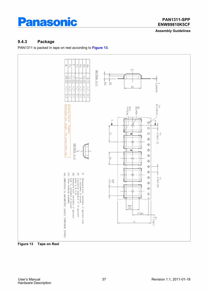
PAN1311-SPPENW89810K5CF
Assembly Guidelines
9.4.3 PackagePAN1311 is packed in tape on reel according to Figure 13.
Figure 13 Tape on Reel
User’s Manual 37 Revision 1.1, 2011-01-18Hardware Description
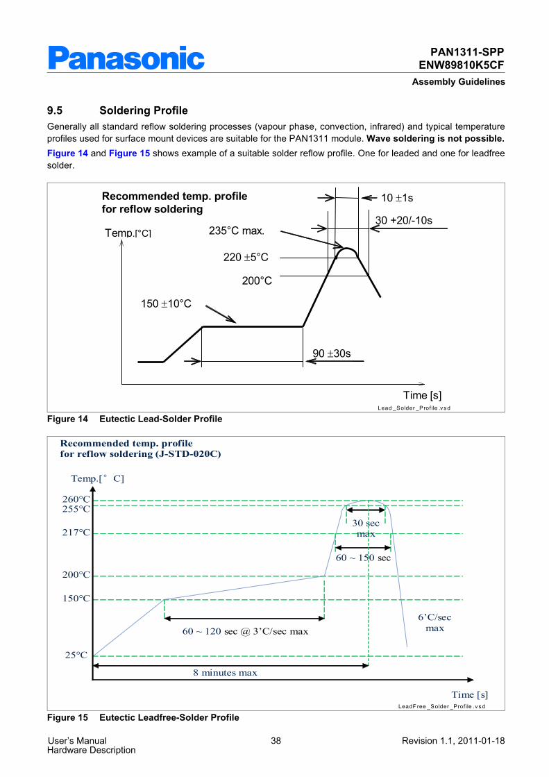
PAN1311-SPPENW89810K5CF
Assembly Guidelines
9.5 Soldering ProfileGenerally all standard reflow soldering processes (vapour phase, convection, infrared) and typical temperature profiles used for surface mount devices are suitable for the PAN1311 module. Wave soldering is not possible.Figure 14 and Figure 15 shows example of a suitable solder reflow profile. One for leaded and one for leadfree solder.
Lead _Solder _Prof ile .v s d
Recommended temp. profile for reflow soldering
Temp.[°C]
Time [s]
235°C max.
220 ±5°C
200°C
150 ±10°C
90 ±30s
10 ±1s
30 +20/-10s
Figure 14 Eutectic Lead-Solder Profile
LeadF ree _Solder _Prof ile .v s d
25°C
150°C
200°C
217°C
255°C 260°C
60 ~ 120 sec @ 3’C/sec max
60 ~ 150 sec
30 sec max
6’C/sec max
8 minutes max
Temp.[°C]
Time [s]
Recommended temp. profile for reflow soldering (J-STD-020C)
Figure 15 Eutectic Leadfree-Solder Profile
User’s Manual 38 Revision 1.1, 2011-01-18Hardware Description

PAN1311-SPPENW89810K5CF
Assembly Guidelines
At the reflow process each solder joint has to be exposed to temperatures above solder liquids for a sufficient time to get the optimum solder joint quality, whereas overheating the board with its components has to be avoided. Using infrared ovens without convection special care may be necessary to assure a sufficiently homogeneous temperature profile for all solder joints on the PCB (especially on large, complex boards with different thermal masses of the components). The most recommended types are therefore forced convection or vapour phase reflow. Nitrogen atmosphere can generally improve solder joint quality, but is normally not necessary.The reflow profiles and other reflow parameters are dependent on the used solder paste. The paste manufacturer provides a reflow profile recommendation for this product.Additionally it is important not to overheat the PAN1311 module by a too large reflow peak temperature. PAN1311contain several plastic packages and is there by sensitive of the moisture content level at the time of board assembly.Overheating in combination with excessive moisture content could result in package delaminations or cracks (popcorn effect). The heating rate should not exceed 3°C/s and max sloping rate should not exceed 4°C/s.PAN1311 shall be handled according to MSL3, which means a floor life of 168h in 30°C/60% r.h.The PAN1311 module can be soldered according to max. J-STD-020C curve, assuming that all other conditions are followed stated in Product Specification, Qualification Report and in Application Note. Restriction is that PAN1311 can be soldered two times, since one time is already consumed when soldering devices on Module.
9.6 Rework
9.6.1 Removal Procedure
1. Heat the module with an appropriate heating nozzle according to the instruction of the equipment or on a hot plate (about 225°C dependent on the board). Hot plate can only be used if the board is single side assembled. The temperature of the module shall be 200-220°C.
2. Use grippers or a pair of tweezers to remove the module. The module has to be gripped on two opposite edges of the module (not on the shield).
3. Remove excess solder by using solder sucker, suction soldering irons or solder wick.
9.6.2 Replacement ProcedureReplacement can be done in two ways, dependent of how the solder is applied. Solder can be applied either by dispensing on the mother board or by printing the solder paste directly on the module.
9.6.2.1 Alternative 1: Dispensing SolderA dispenser with controlled volume must be used to assure the same volume on every pad. The volume on each pad shall be about 0.04 mm3.1. Dispense 0.04 mm3 on each LGA pad2. Pick the module by a nozzle and place in the right position on the board3. Reflow the solder.
User’s Manual 39 Revision 1.1, 2011-01-18Hardware Description

PAN1311-SPPENW89810K5CF
Assembly Guidelines
9.6.2.2 Alternative 2: Printing SolderTo print solder on the module a fixture must be used. The purpose of the fixture is to get a flat surface and fix the stencil and module for printing. An example of how this fixture can be designed is shown in Figure 16.
Solder _Print ing .v s d
Vacuum hol es
Solder paste stencil
C avity of the module Tooling pins
B ottom
Fixture
Figure 16 Solder Printing
1. Assemble the fixture to the bottom2. Place the module in the cavity with the LGA pads upwards3. Place the solder paste stencil on the fixture and make sure it fits to the tooling pins and the module4. Apply vacuum to fix the solder paste stencil5. Apply solder paste on the stencil and print by using a blade6. Turn everything (bottom, fixture and stencil) upside down.7. Separate carefully the bottom from the fixture8. Pick the module by a nozzle and place in the right position on the board9. Reflow the solder.
9.7 InspectionAutomatic inspection of the solder paste printing before assembly is highly recommended to ensure high yield and good long term reliability.
9.8 Component SalvageIf it is intended to send a defect PAN1311 module back to the supplier for failure analysis, please note that during the removal of this component no further defects must be introduced to the device, because this may hinder the failure analysis at the supplier. This includes ESD precautions, not to apply high mechanical force for component removal, and to prevent excess moisture content in the package during salvage (risk of pop corning failures). Therefore if the maximum storage time out of the dry pack (see label on packing material) is exceeded after board assembly, the PCB has to be dried 24h at 125°C before soldering off the defect component, because otherwise too much moisture may have been accumulated.
User’s Manual 40 Revision 1.1, 2011-01-18Hardware Description
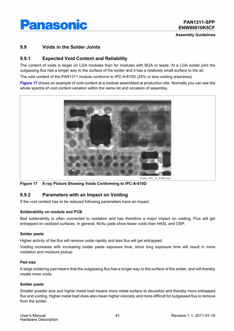
PAN1311-SPPENW89810K5CF
Assembly Guidelines
9.9 Voids in the Solder Joints
9.9.1 Expected Void Content and ReliabilityThe content of voids is larger on LGA modules than for modules with BGA or leads. At a LGA solder joint the outgassing flux has a longer way to the surface of the solder and it has a relatively small surface to the air.The void content of the PAN1311 module conforms to IPC-A-610D (25% or less voiding area/area).Figure 17 shows an example of void-content at a module assembled at production site. Normally you can see the whole spectra of void content variation within the same lot and occasion of assembly.
Voids _IPC _A_ 610D .v s d
Figure 17 X-ray Picture Showing Voids Conforming to IPC-A-610D
9.9.2 Parameters with an Impact on VoidingIf the void content has to be reduced following parameters have an impact.
Solderability on module and PCBBad solderability is often connected to oxidation and has therefore a major impact on voiding. Flux will get entrapped on oxidized surfaces. In general, Ni/Au pads show fewer voids than HASL and OSP.
Solder pasteHigher activity of the flux will remove oxide rapidly and less flux will get entrapped.Voiding increases with increasing solder paste exposure time, since long exposure time will result in more oxidation and moisture pickup.
Pad sizeA large soldering pad means that the outgassing flux has a longer way to the surface of the solder, and will thereby create more voids.
Solder pasteSmaller powder size and higher metal load means more metal surface to deoxidize and thereby more entrapped flux and voiding. Higher metal load does also mean higher viscosity and more difficult for outgassed flux to remove from the solder.
User’s Manual 41 Revision 1.1, 2011-01-18Hardware Description

PAN1311-SPPENW89810K5CF
Assembly Guidelines
Stencil thicknessA thick solder paste stencil means more surface area to the air and thereby easier for the outgassing flux to leave the solder.
Temperature soldering profileToo short preheat time means that the flux does not get enough time to react and flux get entrapped in the solder and create voids.Too long reflow time gives larger voidsToo short reflow time gives a fraction of voids
User’s Manual 42 Revision 1.1, 2011-01-18Hardware Description

PAN1311-SPPENW89810K5CF
Terminology
Terminology
AACK AcknowledgementARQ Automatic Repeat reQuestBb bit/bits (e.g. kb/s)B Byte/Bytes (e.g. kB/s)BALUN BALanced UNbalancedBD_ADDR Bluetooth Device AddressBER Bit Error RateBMU BlueMoon UniversalBOM Bill Of MaterialBT BluetoothBW BandwidthCCMOS Complementary Metal Oxide SemiconductorCOD Class Of DeviceCODEC COder/DECoderCPU Central Processing UnitCQDDR Channel Quality Driven Data RateCRC Cyclic Redundancy CheckCTS Clear To Send (UART flow control signal)CVSD Continuous Variable Slope Delta (modulation)CDCT Clock Drift Compensation TaskCQDDR Channel Quality Driven Data RateDDC Direct CurrentDDC Device Data ControlDM Data Medium-Rate (packet type)DMA Direct Memory AccessDH Data High-Rate (packet type)DPSK Differential Phase Shift Keying (modulation)DQPSK Differential Quaternary Phase Shift Keying (modulation)DSP Digital Signal ProcessorDUT Device Under Test
EEDR Enhanced Data RateEEPROM Electrically Erasable Programmable Read Only Memory
User’s Manual 43 Revision 1.1, 2011-01-18Hardware Description
PAN1311-SPPENW89810K5CF
Terminology
eSCO Extended Synchronous Connection-Oriented (logical transport)EV Extended Voice (packet type)FFEC Forward Error CorrectionFHS Frequency Hop Synchronization (packet)FIFO First In First Out (buffer)FM Frequency ModulationFW FirmwareGGFSK Gaussian Frequency Shift Keying (modulation)GPIO General Purpose Input/OutputGSM Global System for Mobile communicationHHCI Host Controller InterfaceHCI+ Infineon Specific HCI command setHEC Header Error CheckHV High quality Voice (packet type)HW HardwareII2C Inter-IC Control (bus)I2S Inter-IC Sound (bus)IAC Inquiry Access CodeID IDentifierIEEE Institute of Electrical and Electronics EngineersIF Intermediate FrequencyISM Industrial Scientific & Medical (frequency band)JJTAG Joint Test Action GroupLLAN Local Area NetworkLAP Lower Address PartLM Link ManagerLMP Link Manager ProtocolLNA Low Noise AmplifierLO Local OscillatorLPM Low Power Mode(s)LPO Low Power OscillatorLSB Least Significant Bit/ByteLT_ADDR Logical Transport AddressM
User’s Manual 44 Revision 1.1, 2011-01-18Hardware Description
PAN1311-SPPENW89810K5CF
Terminology
MSB Most Significant Bit/ByteMSRS Master-Slave Role SwitchNNC No ConnectionNOP No OPerationNVM Non-Volatile MemoryOOCF Opcode Command FieldOGF Opcode Group FieldPPA Power AmplifierPCB Printed Circuit BoardPCM Pulse Coded ModulationPDU Protocol Data UnitPER Packet Error RatePIN Personal Identification NumberPLC Packet Loss ConcealmentPLL Phase Locked LoopPMU Power Management UnitPOR Power-On ResetPTA Packet Traffic ArbitrationPTT Packet Type TableQQoS Quality Of ServiceRRAM Random Access MemoryRF Radio FrequencyROM Read Only MemoryRSSI Received Signal Strength IndicationRTS Request To Send (UART flow control signal)RX ReceiveRXD Receive Data (UART signal)SSCO Synchronous Connection-Oriented (logical transport)SIG Special Interest Group (Bluetooth SIG)SW SoftwareSYRI Synthesizer Reference InputTTBD To Be DeterminedTCK Test Clock (JTAG signal)
User’s Manual 45 Revision 1.1, 2011-01-18Hardware Description
PAN1311-SPPENW89810K5CF
Terminology
TDI Test Data In (JTAG signal)TDO Test Data Out (JTAG signal)TL Transport LayerTMS Test Mode Select (JTAG signal)TX TransmitTXD Transmit Data (UART signal)UUART Universal Asynchronous Receiver & TransmitterULPM Ultra Low Power ModeVVCO Voltage Controlled OscillatorWWLAN Wireless LAN (Local Area Network)
User’s Manual 46 Revision 1.1, 2011-01-18Hardware Description

PAN1311-SPPENW89810K5CF
User’s Manual 47 Revision 1.1, 2011-01-18Hardware Description
References
References[1] SPP-AT Application on PAN1311; Software Version 1.1; Release Notes; Rev3.0
(PAN1311_SPP_AT_V10.03_V1.1_RN_Rev3.0.pdf)
[2] SPP-AT User's Manual Software Description ; Rev3.0 (PAN1311_SPP_AT_V10.03_V1.1_UM_SD_Rev3.0.pdf)

Published by Panasonic Electronic Devices Europe GmbH
w w w . p e d e u . p a n a s o n i c . d e