Embed Size (px)
Citation preview

PAE
B-65・All specifications are subject to change without notice.
PAE100S48-5
PAE100S48-3R3/HV
PAE SERIES
Product Line up
DC-DC Module 50W, 100W
Applications
PAE-S48(DC48Vin)
Output Voltage50W 100W
Output Current Model Output Current Model1.8V 20A PAE50S48-1R8 30A PAE100S48-1R82.5V 18A PAE50S48-2R5 25A PAE100S48-2R5
3.3V 16A PAE50S48-3R325A PAE100S48-3R330A PAE100S48-3R3/H
5V 10A PAE50S48-5 20A PAE100S48-5
医 療 計 測 F A 半導体 その他
その他ks
コンピュータ 通 信 F A 半導体
その他ph
pf-a
hk-a
hws
alpha
dlp
fps
フォーマット
コンピュータ 通 信 F A 半導体
その他
コンピュータ 通 信 医 療 計 測 F A 半導体
その他
コンピュータ 通 信 医 療 計 測 F A 半導体
その他
コンピュータ 通 信 医 療 計 測 F A 半導体
その他
コンピュータ 通 信 医 療 計 測 F A 半導体
その他
医 療 計 測 F A 半導体 その他
その他ks
コンピュータ 通 信 F A 半導体
その他ph
pf-a
hk-a
hws
alpha
dlp
fps
フォーマット
コンピュータ 通 信 F A 半導体
その他
コンピュータ 通 信 医 療 計 測 F A 半導体
その他
コンピュータ 通 信 医 療 計 測 F A 半導体
その他
コンピュータ 通 信 医 療 計 測 F A 半導体
その他
コンピュータ 通 信 医 療 計 測 F A 半導体
その他
PAE 100 S 48 − 1R8 / Option Blank: OVP manual reset V: OVP auto-recovery
Nominal output voltageNominal input voltageFunctionS: Simple function
Output powerSeries name
PAE-S24(DC24Vin)
Output Voltage50W
Output Current Model5V 10A PAE50S24-56V 8.4A PAE50S24-6
YEARS
warranty2
Features Design meeting RoHS (the fifth generation) 1/8 brick industry standard size (22.76mm×8.5mm×57.9mm) 100W output in 1/8 brick size (PAE100S48-5) Power density: 146.3W/inch3 (PAE100S48-5) High efficiency: 91% (3.3V output, 5V output, /H : 90%) Basic insulation between input and output Internal capacitor: Ceramic capacitor only (high reliability)
Model naming method
This means that, in conformity with EU Directive 2002/95/ EC, lead, cadmium, mercury, hexavalent chromium, and specific bromine-based flame retardants, PBB and PBDE, have not been used, except for exempted applications.
Conformity to RoHS Directive
PAE
B-66 ・All specifications are subject to change without notice.
PAE50S24
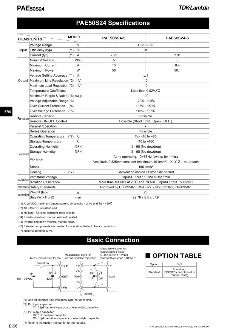
PAE50S48 PAE50S24 Specifications
Basic Connection
+Vin
-Vin
CNT
+Vin
-Vin
Vin
18V - 36VDC
Fuse 6.3A
Measurement point for VinMeasurement point for Vo and load/line regulation
Measurement point for output riople & noise(JEITA RC-9141 probe)Bandwidth of scope : 100MHz
CNT
+V
+S *3C2
1uF
50mm
C3*2
*1
C1
33uF+10uF
Load
++
-
-S
-V
TRM
(*1) Use an external fuse (fast blow type) for each unit.
(*2) Put input capacitor. C1: 33µF ceramic capacitor or electrolytic capacitor
(*3) Put output capacitor. C2: 1µF ceramic capacitor C3: 10µF tantalum capacitor or electrolytic capacitor
(*4) Refer to instruction manual for further details.
ITEMS/UNITS MODEL PAE50S24-5 PAE50S24-6
Input
Voltage Range V DC18 - 36
Efficiency (typ) (*1) % 91
Current (typ) (*1) A 2.29 2.31
Output
Nominal Voltage VDC 5 6
Maximum Current A 10 8.4
Maximum Power W 50 50.4
Voltage Setting Accuracy (*1) % ±1
Maximum Line Regulation (*2) mV 10
Maximum Load Regulation (*3) mV 10
Temperature Coefficient Less than 0.02%/Maximum Ripple & Noise (*6) mVp-p 100
Voltage Adjustable Range (*6) -20%, +10%
Function
Over Current Protection (*4) 105% - 150%
Over Voltage Protection (*5) 115% - 135%
Remote Sensing Possible
Remote ON/OFF Control Possible (Short : ON, Open : OFF )
Parallel Operation -
Series Operation Possible
Environment
Operating Temperature (*7) Ta= -40 to +85
Storage Temperature -40 to +100
Operating Humidity %RH 5 - 95 (No dewdrop)
Storage Humidity %RH 5 - 95 (No dewdrop)
Vibration At no operating, 10~55Hz (sweep for 1min.)
Amplitude 0.825mm constant (maximum 49.0m/s²) X, Y, Z 1 hour each
Shock 196.1m/s²
Cooling (*7) Convection cooled / Forced air cooled
IsolationWithstand Voltage Input-Output : 1.5kVDC for 1min
Isolation Resistance More than 100MΩ at 25 and 70%RH Input-Output...500VDC
Standards Safety Standards Approved by UL60950-1, CSA C22.2 No.60950-1, EN60950-1
MechanicalWeight (typ) g 25
Size (W x H x D) mm 22.76 x 8.5 x 57.9
(*1) At 24VDC, maximum output current, air velocity = 2m/s and Ta = +25.
(*2) 18 - 36VDC, constant load.
(*3) No load - full load, constant input voltage.
(*4) Inverter shutdown method with auto restart.
(*5) Inverter shutdown method, manual reset.
(*6) External components are needed for operation. Refer to basic connection.
(*7) Refer to derating curve.
Option OVP
StandardShut down
(ON/OFF control reset or manual reset)
OPTION TABLE
PAE
B-67・All specifications are subject to change without notice.
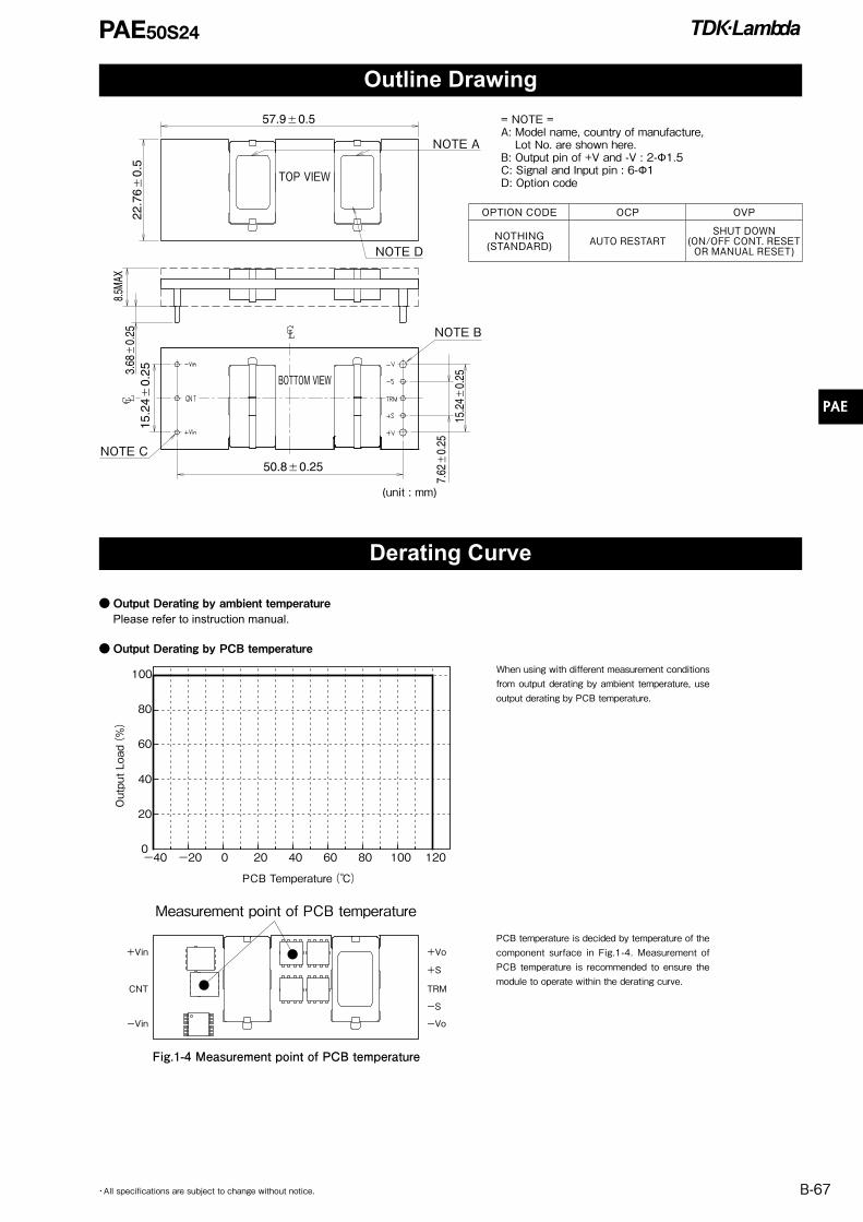
PAE50S24
Outline Drawing
Derating Curve
Measurement point of PCB temperature
+Vo
+S
TRM
ーS
ーVo
+Vin
CNT
ーVin
Fig.1-4 Measurement point of PCB temperature
Output Derating by PCB temperature
Output Derating by ambient temperature Please refer to instruction manual.
PCB Temperature()
-40 -20 0 20 40 60 80 100
20
100
0
40
60
80
120
Output Load(%)
注1
注1. 型名・製造国名および安全規格が表示されます。注2. ターミナルピン 出力ピン: 2-φ1.5注3. ターミナルピン 入力・信号ピン: 6-φ1注4. オプションコード
型名
無(標準モデル)
/V
過電圧保護OVP
出力遮断ON/OFFコントロールによるリセット方式または入力再投入の手動リセット可能
自動復帰型
注4
上面
下面
注2
注3
NOTE A
= NOTE =A: Model name, country of manufacture, Lot No. are shown here.B: Output pin of +V and -V : 2-Φ1.5C: Signal and Input pin : 6-Φ1D: Option code
NOTE D
TOP VIEW
BOTTOM VIEW
NOTE B
NOTE C
型 名
PAE50S24-**(標準モデル)
PAE50S24-**/V
過電流保護 (OCP)
自動復帰型
自動復帰型
過電圧保護 (OVP)
出力遮断型
自動復帰型
「出力遮断型」のリセット法 : ON/OFFコントロール、または、入力遮断/再投入による手動リセットです。
(unit : mm)
OPTION CODE OCP OVP
NOTHING(STANDARD) AUTO RESTART
SHUT DOWN(ON/OFF CONT. RESET OR MANUAL RESET)
When using with different measurement conditions from output derating by ambient temperature, use output derating by PCB temperature.
PCB temperature is decided by temperature of the component surface in Fig.1-4. Measurement of PCB temperature is recommended to ensure the module to operate within the derating curve.
PAE
B-68 ・All specifications are subject to change without notice.
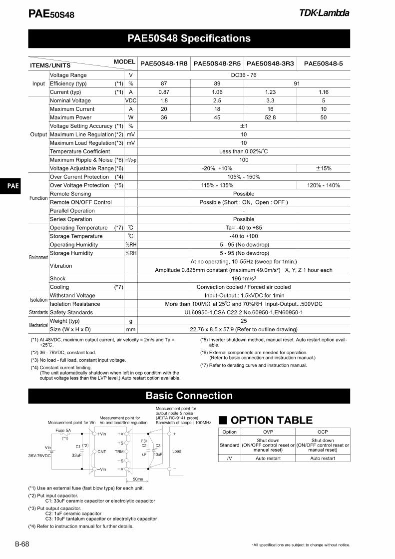
PAE50S48 Specifications
PAE50S48
Basic Connection
+
-
Load10uF
C3
luF
50mm
C2(*3)
+
-V
-S
+S
TRMCNT33uF
C1(*2)
(*1)
Fuse 5A+V+Vin
-Vin
Vin
36V-76VDC
Measurement point for VinMeasurement point forVo and load/line reguation
Measurement point foroutput ripple & noise(JEITA RC-9141 probe)Bandwidth of scope : 100MHz
ITEMS/UNITS MODEL PAE50S48-1R8 PAE50S48-2R5 PAE50S48-3R3 PAE50S48-5
Input
Voltage Range V DC36 - 76
Efficiency (typ) (*1) % 87 89 91
Current (typ) (*1) A 0.87 1.06 1.23 1.16
Output
Nominal Voltage VDC 1.8 2.5 3.3 5
Maximum Current A 20 18 16 10
Maximum Power W 36 45 52.8 50
Voltage Setting Accuracy (*1) % ±1
Maximum Line Regulation (*2) mV 10
Maximum Load Regulation (*3) mV 10
Temperature Coefficient Less than 0.02%/Maximum Ripple & Noise (*6) mVp-p 100
Voltage Adjustable Range (*6) -20%, +10% ±15%
Function
Over Current Protection (*4) 105% - 150%
Over Voltage Protection (*5) 115% - 135% 120% - 140%
Remote Sensing Possible
Remote ON/OFF Control Possible (Short : ON, Open : OFF )
Parallel Operation -
Series Operation Possible
Environment
Operating Temperature (*7) Ta= -40 to +85
Storage Temperature -40 to +100
Operating Humidity %RH 5 - 95 (No dewdrop)
Storage Humidity %RH 5 - 95 (No dewdrop)
Vibration At no operating, 10-55Hz (sweep for 1min.)
Amplitude 0.825mm constant (maximum 49.0m/s²) X, Y, Z 1 hour each
Shock 196.1m/s²
Cooling (*7) Convection cooled / Forced air cooled
IsolationWithstand Voltage Input-Output : 1.5kVDC for 1min
Isolation Resistance More than 100MΩ at 25 and 70%RH Input-Output...500VDC
Standards Safety Standards UL60950-1,CSA C22.2 No.60950-1,EN60950-1
MechanicalWeight (typ) g 25
Size (W x H x D) mm 22.76 x 8.5 x 57.9 (Refer to outline drawing)
(*1) At 48VDC, maximum output current, air velocity = 2m/s and Ta = +25.
(*2) 36 - 76VDC, constant load.
(*3) No load - full load, constant input voltage.
(*4) Constant current limiting. (The unit automatically shutdown when left in ocp conditim with the
output voltage less than the LVP level.) Auto restart option available.
(*1) Use an external fuse (fast blow type) for each unit.
(*2) Put input capacitor. C1: 33uF ceramic capacitor or electrolytic capacitor
(*3) Put output capacitor. C2: 1uF ceramic capacitor C3: 10uF tantalum capacitor or electrolytic capacitor
(*4) Refer to instruction manual for further details.
Option OVP OCP
StandardShut down
(ON/OFF control reset or manual reset)
Shut down(ON/OFF control reset or
manual reset)
/V Auto restart Auto restart
OPTION TABLE
(*5) Inverter shutdown method, manual reset. Auto restart option avail-able.
(*6) External components are needed for operation. (Refer to basic connection and instruction manual.)
(*7) Refer to derating curve and instruction manual.
PAE
B-69・All specifications are subject to change without notice.
PAE50S48
注1
注1. 型名・製造国名および安全規格が表示されます。注2. ターミナルピン 出力ピン: 2-φ1.5注3. ターミナルピン 入力・信号ピン: 6-φ1注4. オプションコード
型名
無(標準モデル)
/V
過電圧保護OVP
出力遮断ON/OFFコントロールによるリセット方式または入力再投入の手動リセット可能
自動復帰型
注4
上面
下面
注2
注3
NOTE A
(*1) 型名・製造国名およびロットNo.が表示されます。(*2) ターミナルピン 出力ピン: 2-φ1.5(*3) ターミナルピン 入力・信号ピン: 6-φ1(*4) 安全規格が表示されます。(*5) オプションコード
NOTE D
TOP VIEW
BOTTOMVIEW
NOTE B
NOTEC
型 名
PAE50S24-**(標準モデル)
PAE50S24-**/V
過電流保護 (OCP)
自動復帰型
自動復帰型
過電圧保護 (OVP)
出力遮断型
自動復帰型
「出力遮断型」のリセット法 : ON/OFFコントロール、または、入力遮断/再投入による手動リセットです。
Measurement point of PCB temperature
+Vo
+S
TRM
ーS
ーVo
+Vin
CNT
ーVin
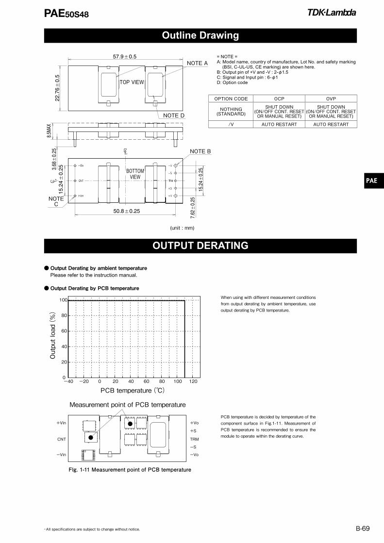
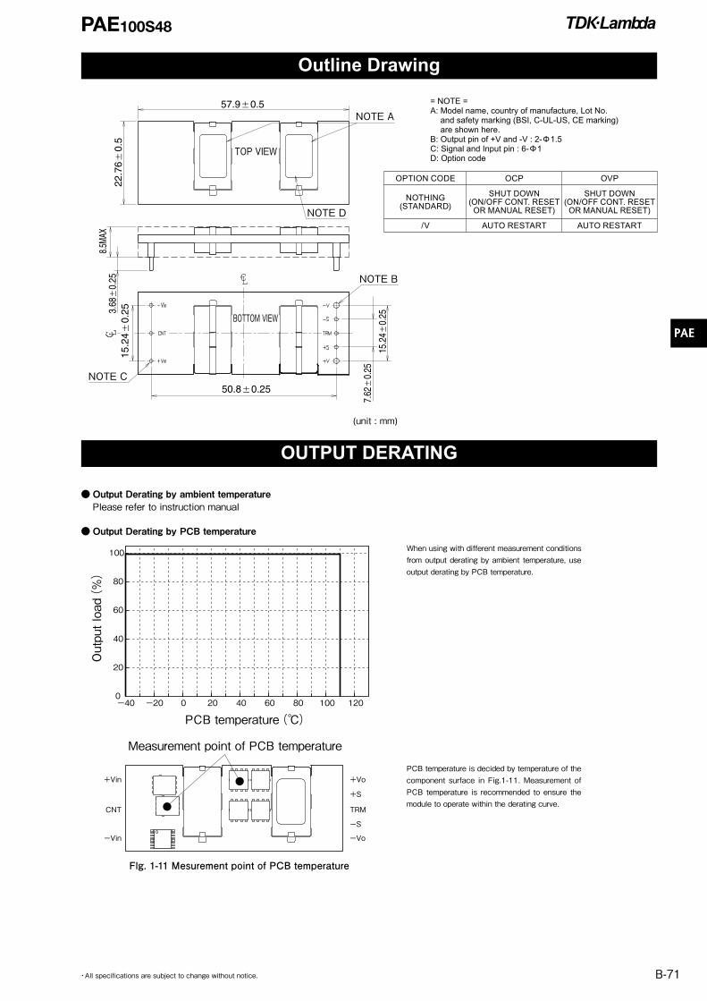
Outline Drawing
OUTPUT DERATING
(unit : mm)
= NOTE =A: Model name, country of manufacture, Lot No. and safety marking
(BSI, C-UL-US, CE marking) are shown here.B: Output pin of +V and -V : 2-φ1.5C: Signal and Input pin : 6-φ1D: Option code
Flg. 1-11 Measurement point of PCB temperature
Output Derating by ambient temperature Please refer to the instruction manual.
When using with different measurement conditions from output derating by ambient temperature, use output derating by PCB temperature.
Output Derating by PCB temperature
PCB temperature()-40 -20 0 20 40 60 80 100
20
100
0
40
60
80
120
Output load(%)
OPTION CODE OCP OVP
NOTHING(STANDARD)
SHUT DOWN(ON/OFF CONT. RESET OR MANUAL RESET)
SHUT DOWN(ON/OFF CONT. RESET OR MANUAL RESET)
/V AUTO RESTART AUTO RESTART
PCB temperature is decided by temperature of the component surface in Fig.1-11. Measurement of PCB temperature is recommended to ensure the module to operate within the derating curve.

PAE
B-70 ・All specifications are subject to change without notice.
PAE100S48
PAE100S48 Specifications
ITEMS/UNITS MODEL PAE100S48-1R8 PAE100S48-2R5 PAE100S48-3R3 PAE100S48-3R3/H PAE100S48-5
Input
Voltage Range V DC36 - 76
Efficiency (typ) (*1) % 87 89 91 90 91
Current (typ) (*1) A 1.30 1.47 1.89 2.3 2.29
Output
Nominal Voltage VDC 1.8 2.5 3.3 3.3 5
Maximum Current A 30 25 30 20
Maximum Power W 54 62.5 82.5 99 100
Voltage Setting Accuracy (*1) % ±1
Maximum Line Regulation (*2) mV 10
Maximum Load Regulation (*3) mV 10
Temperature Coefficient Less than 0.02%/Maximum Ripple & Noise (*6) mVp-p 100
Voltage Adjustable Range (*6) -20%, +10% ±15%
Function
Over Current Protection (*4) 105% - 150%
Over Voltage Protection (*5) 115% - 135% 120% - 140%
Remote Sensing Possible
Remote ON/OFF Control Possible (Short : ON, Open : OFF )
Parallel Operation -
Series Operation Possible
Environment
Operating Temperature (*7) Ta= -40 to +85
Storage Temperature -40 to +100
Operating Humidity %RH 5 - 95 (No dewdrop)
Storage Humidity %RH 5 - 95 (No dewdrop)
Vibration At no operating, 10-55Hz (sweep for 1min.)
Amplitude 0.825mm constant (maximum 49.0m/s²) X, Y, Z 1 hour each
Shock 196.1m/s²
Cooling (*7) Convection cooled / Forced air cooled
IsolationWithstand Voltage Input-Output : 1.5kVDC for 1min
Isolation Resistance More than 100MΩ at 25 and 70%RH Input-Output...500VDC
Standards Safety Standards Approved by UL60950-1, CSA C22.2 No.60950-1, EN60950-1
MechanicalWeight (typ) g 25
Size (W x H x D) mm 22.76 x 8.5 x 57.9 (Refer to outline drawing)
(*1) At 48VDC, maximum output current, air velocity = 2m/s and Ta = +25.
(*2) 36 - 76VDC, constant load.
(*3) No load - full load, constant input voltage.
(*4) Constant current limiting. (The unit automatically shutdown when left in OCP condition with
the output voltage less than the LVP level.) Auto restart option
available.
(*5) Inverter shutdown method, manual reset. Auto restart option avail-able.
(*6) External components are needed for operation. (Refer to basic connection and instruction manual.)
(*7) Refer to derating curve and instruction manual.
Basic Connection
(*1) Use an external fuse (fast blow type) for each unit.
(*2) Put input capacitor. C1: 33uF ceramic capacitor or electrolytic capacitor
(*3) Put output capacitors. C2: 1uF ceramic capacitor C3: 10uF tantalum capacitor or electrolytic capacitor
(*4) Refer to instruction manual for further details.
+Vin
-Vin
CNT
+Vin
-Vin
Vin
36V - 76VDC
Fuse 6.3A
Measurement point for VinMeasurement point for Vo and load/line regulation
Measurement point for output riople & noise(JEITA RC-9141 probe)Bandwidth of scope : 100MHz
CNT
+V
+S *3C2
1uF
50mm
C3*2
*1
C1
33uF+10uF
Load
++
-
-S
-V
TRM
Option OVP OCP
StandardShut down
(ON/OFF control reset or manual reset)
Shut down(ON/OFF control reset or
manual reset)
/V Auto restart Auto restart
OPTION TABLE
PAE
B-71・All specifications are subject to change without notice.
Outline Drawing
PAE100S48
(unit : mm)
注1
注1. 型名・製造国名および安全規格が表示されます。注2. ターミナルピン 出力ピン: 2-φ1.5注3. ターミナルピン 入力・信号ピン: 6-φ1注4. オプションコード
型名
無(標準モデル)
/V
過電圧保護OVP
出力遮断ON/OFFコントロールによるリセット方式または入力再投入の手動リセット可能
自動復帰型
注4
上面
下面
注2
注3
NOTE A
(*1) 型名・製造国名およびロットNo.が表示されます。(*2) ターミナルピン 出力ピン: 2-φ1.5(*3) ターミナルピン 入力・信号ピン: 6-φ1(*4) 安全規格が表示されます。(*5) オプションコード
NOTE D
TOP VIEW
BOTTOM VIEW
NOTE B
NOTE C
型 名
PAE50S24-**(標準モデル)
PAE50S24-**/V
過電流保護 (OCP)
自動復帰型
自動復帰型
過電圧保護 (OVP)
出力遮断型
自動復帰型
「出力遮断型」のリセット法 : ON/OFFコントロール、または、入力遮断/再投入による手動リセットです。
= NOTE =A: Model name, country of manufacture, Lot No.
and safety marking (BSI, C-UL-US, CE marking) are shown here.
B: Output pin of +V and -V : 2-Φ1.5C: Signal and Input pin : 6-Φ1D: Option code
Output Derating by PCB temperature
PCB temperature()-40 -20 0 20 40 60 80 100
20
100
0
40
60
80
120
Output load(%)
Measurement point of PCB temperature
+Vo
+S
TRM
ーS
ーVo
+Vin
CNT
ーVin
OUTPUT DERATING
Flg. 1-11 Mesurement point of PCB temperature
Output Derating by ambient temperature Please refer to instruction manual
When using with different measurement conditions from output derating by ambient temperature, use output derating by PCB temperature.
PCB temperature is decided by temperature of the component surface in Fig.1-11. Measurement of PCB temperature is recommended to ensure the module to operate within the derating curve.
OPTION CODE OCP OVP
NOTHING(STANDARD)
SHUT DOWN(ON/OFF CONT. RESET
OR MANUAL RESET)
SHUT DOWN(ON/OFF CONT. RESET
OR MANUAL RESET)
/V AUTO RESTART AUTO RESTART
PAE
B-72 ・All specifications are subject to change without notice.
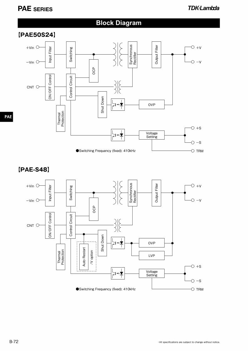
Block Diagram
OVP
VoltageSetting
+S
-S
TRMSwitching Frequency (fixed): 410kHz
+Vin
-Vin
+V
-V
CNT
Input Filter
Switching
ON/OFF Control
Control Circuit
Thermal
Protection Shut Down
OCP
Synchronous
Rectifier
Output Filter
PAE SERIES
【PAE-S48】
【PAE50S24】
OVP
+S
-S
TRMSwitching Frequency (fixed): 410kHz
+Vin
-Vin
+V
-V
CNT
Input Filter
Switching
ON/OFF Control
Control Circuit
Auto Restart
/V option Shut Down
OCP
Synchronous
Rectifier
Output Filter
LVP
VoltageSetting
Thermal
Protection
PAE
B-73・All specifications are subject to change without notice.
Input Voltage
Output Voltage
ON/OFFControl
Input ON
Control OFF
Control ON
Control OFF
Control ON
OTP trip
OTP reset
Input OFF
OVP trip
OCP trip
Input ON
OCP release
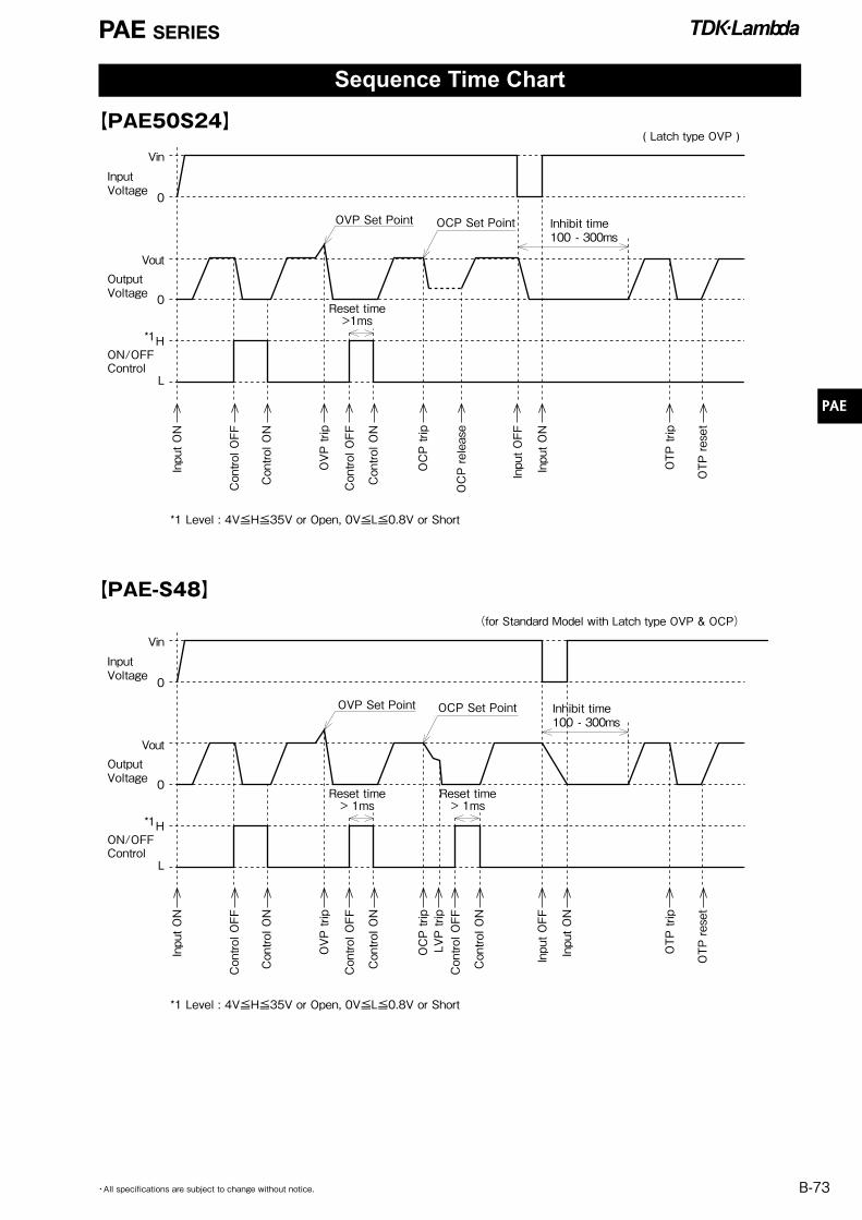
*1 Level : 4V≦H≦35V or Open, 0V≦L≦0.8V or Short
OVP Set Point
Reset time>1ms
OCP Set Point
Vin
0
Vout
0
H
L
*1
Inhibit time100 - 300ms
Sequence Time Chart
PAE SERIES
【PAE-S48】
【PAE50S24】 ( Latch type OVP )
Input Voltage
Output Voltage
ON/OFFControl
Input ON
Control OFF
Control ON
Control OFF
Control ON
OTP trip
OTP reset
Input OFF
Control OFF
Control ON
OVP trip
OCP trip
LVP trip
Input ON
*1 Level : 4V≦H≦35V or Open, 0V≦L≦0.8V or Short
OVP Set Point
Reset time> 1ms
Reset time> 1ms
OCP Set Point
Vin
0
Vout
0
H
L
*1
Inhibit time100 - 300ms
(for Standard Model with Latch type OVP & OCP)
PAE 50S24
PAE
B-74 ・All specifications are subject to change without notice.
PAE50S24 SERIES Instruction Manual
Be sure to take note of precautions and warnings indicated in this manual when using this product. Improper usage may lead to electric shock or fire. Be sure to read this instruction manual thoroughly before using this product.
Caution
There are high voltage and high temperature components within this product. Refrain from disassembling this product or touching its internal components as this may lead to elec-tric shock or burned.
When the unit is operating, keep your hands and face away from the unit. You may get injured by accident.
Confirm connections to input/output terminals and signal ter-minals are correct as indicated in the instruction manual.
Attach a fast blow type external fuse to each module to ensure safety operation and compliance to each safety stan-dard approval.
This power module is designed for professional installation within the end user equipment.
Use isolated voltage by reinforced or double insulation as input power source.
Do not inject abnormal voltage to output terminal and signal terminal from the outside.The injection of reverse voltage or over voltage exceeding nominal output voltage to output terminals might cause damage to internal circuit.
The application circuits and their parameter are for reference only. Be sure to verify effectiveness of application circuits and their parameters before finalizing circuit design.
The information in this document is subject to change with-out prior notice. For actual design-in, please refer to the lat-est publications of data sheet, etc., for the most up-to date specifications of the unit.
No part of this document may be copied or reproduced in any for, or by any mean without prior written consent of Den-sei-Lambda.
This product is not authorized for use as critical components in life support devices or systems without prior written con-sent of Densei-Lambda. As used herein:
1. Life support devices or systems are devices or systems which, (a) are intended for surgical implant into the body, or (b) support or sustain life, and whose failure to perform when properly used in accordance with instructions for use provided in the labeling, can be reasonably expected to result in a significant injury to the user.
2. A critical component is any component of a life support device or system whose failure to perform can be reason-ably expected to cause the failure of the life support de-vice or system, or to affect its safety or effectiveness.
Before Using This Power Module
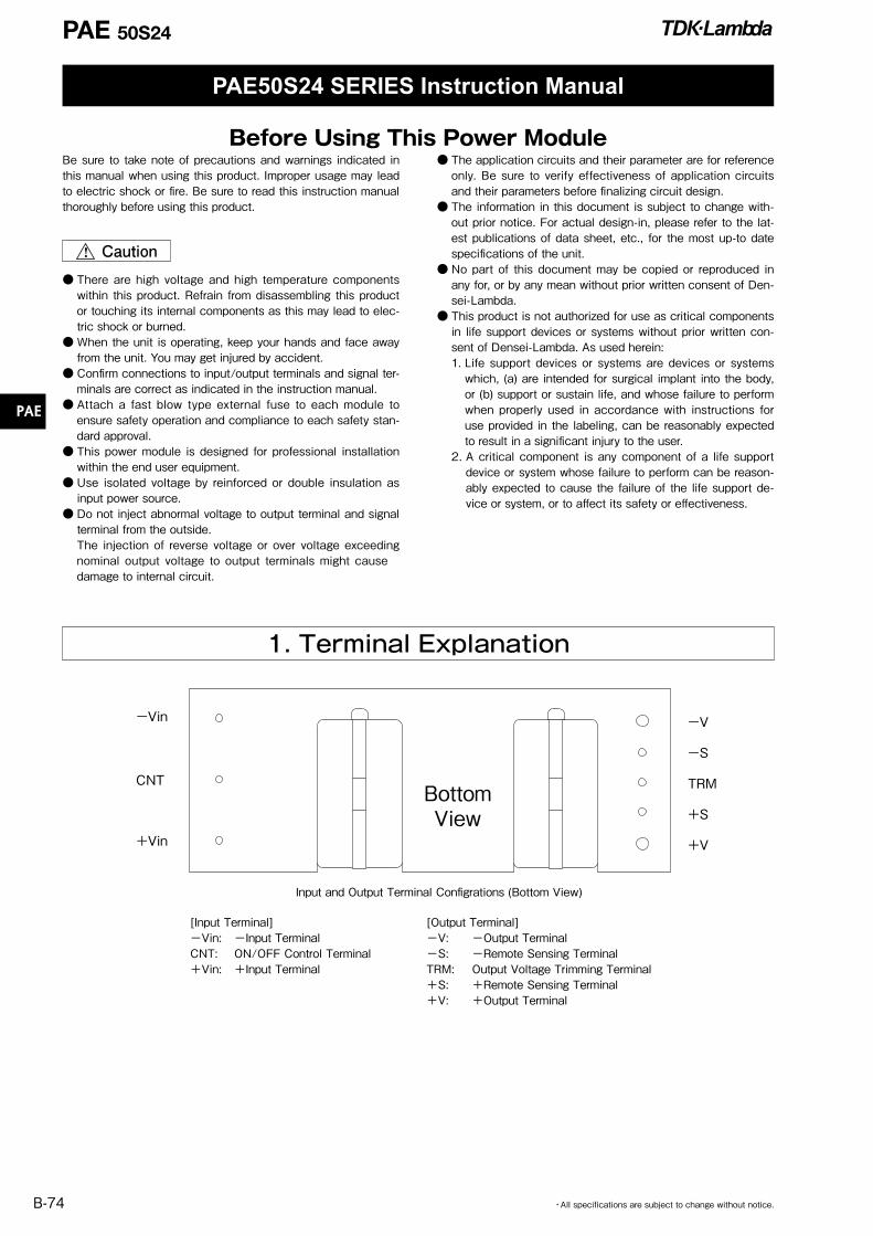
1. Terminal Explanation
[Input Terminal]−Vin: −Input TerminalCNT: ON/OFF Control Terminal+Vin: +Input Terminal
[Output Terminal]−V: −Output Terminal−S: −Remote Sensing TerminalTRM: Output Voltage Trimming Terminal+S: +Remote Sensing Terminal+V: +Output Terminal
Input and Output Terminal Configrations (Bottom View)
BottomView
-Vin -V
+V
-S
+S
TRM
+Vin
CNT
PAE 50S24
PAE
B-75・All specifications are subject to change without notice.
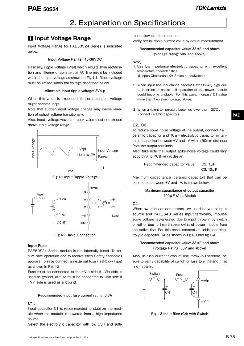
1 Input Voltage RangeInput Voltage Range for PAE50S24 Series is indicated below.
Input Voltage Range : 18-36VDC
Basically, ripple voltage (Vrpl) which results from rectifica-tion and filtering of commercial AC line might be included within the input voltage as shown in Fig.1-1. Ripple voltage must be limited within the voltage described below.
Allowable input ripple voltage: 2Vp-p
When this value is exceeded, the output ripple voltage might become large.Note that sudden input voltage change may cause varia-tion of output voltage transitionally.Also, input voltage waveform peak value must not exceed above input voltage range.
Input Voltage
Range
Time
Input Voltage
Vrpl
t
below 2V
Fig.1-1 Input Ripple Voltage
+
-++
+Vin
50mm
+V
+S
-V
-S
TRM
-Vin
C1
C2
Load
C3
CNT
Fuse
Fig.1-2 Basic Connection
Input FusePAE50S24 Series module is not internally fused. To en-sure safe operation and to receive each Safety Standards approval, please connect an external fuse (fast-blow type) as shown in Fig.1-2.Fuse must be connected to the +Vin side if –Vin side is used as ground, or fuse must be connected to –Vin side if +Vin side is used as a ground.
Recommended input fuse current rating: 6.3A
C1 : Input capacitor C1 is recommended to stabilize the mod-ule when the module is powered from a high impedance source.Select the electrolytic capacitor with low ESR and suffi-
cient allowable ripple current. Verify actual ripple current value by actual measurement.
Recommended capacitor value: 33μF and above(Voltage rating: 50V and above)
Note)1. Use low impedance electrolytic capacitor with excellent
temperature characteristics.(Nippon Chemicon LXV Series or equivalent)
2. When input line inductance becomes excessively high due to insertion of choke coil operation of the power module could become unstable. For this case, increase C1 value more than the value indicated above.
3. When ambient temperature becomes lower than –20 ,connect ceramic capacitors.
C2, C3To reduce spike noise voltage at the output, connect 1μF ceramic capacitor and 10μF electrolytic capacitor or tan-talum capacitor between +V and –V within 50mm distance from the output terminals.Also, take note that output spike noise voltage could vary according to PCB wiring design.
Recommended capacitor value C2: 1μF C3: 10μF
Maximum capacitance (ceramic capacitor) that can be connected between +V and –V, is shown below.
Maximum capacitance of output capacitor400μF (ALL Model)
C4:When switches or connectors are used between input source and PAE_S48 Series input terminals, impulse surge voltage is generated due to input throw-in by switch on/off or due to inserting/removing of power module from the active line. For this case, connect an additional elec-trolytic capacitor C4 as shown in fig.1-3 and fig.1-4.
Recommended capacitor value: 33μF and above(Voltage Rating: 50V and above)
Also, in-rush current flows at line throw-in.Therefore, be sure to verify capability of switch or fuse to withstand I2t at line throw-in.
+Vin+ +
-Vin
FuseSwitch
C4 C1
Fig.1-3 Input filter (C4) with Switch
2. Explanation on Specifications
PAE 50S24
PAE
B-76 ・All specifications are subject to change without notice.
+Vin
-Vin
+Vin
-Vin
FuseSwitch
Fuse
+
C4+
C1
+
C1’
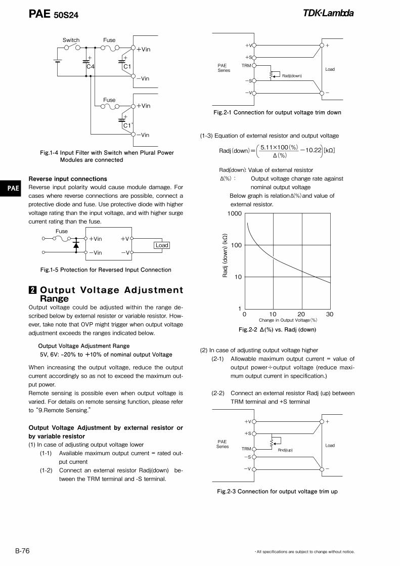
Fig.1-4 Input Filter with Switch when Plural Power Modules are connected
Reverse input connectionsReverse input polarity would cause module damage. For cases where reverse connections are possible, connect a protective diode and fuse. Use protective diode with higher voltage rating than the input voltage, and with higher surge current rating than the fuse.
Fuse+Vin +V
-Vin -VLoad
Fig.1-5 Protection for Reversed Input Connection
2 Output Voltage Adjustment Range
Output voltage could be adjusted within the range de-scribed below by external resister or variable resistor. How-ever, take note that OVP might trigger when output voltage adjustment exceeds the ranges indicated below.
Output Voltage Adjustment Range 5V, 6V: –20% to +10% of nominal output Voltage
When increasing the output voltage, reduce the output current accordingly so as not to exceed the maximum out-put power.Remote sensing is possible even when output voltage is varied. For details on remote sensing function, please refer to “9.Remote Sensing.”
Output Voltage Adjustment by external resistor or by variable resistor (1) In case of adjusting output voltage lower
(1-1) Available maximum output current = rated out-put current
(1-2) Connect an external resistor Radj(down) be-tween the TRM terminal and -S terminal.
+
-
Load Radj(down)
+S
+V
-V
-S
TRM PAE Series
Fig.2-1 Connection for output voltage trim down
(1-3) Equation of external resistor and output voltage
-Radj(down)=Δ(%) 1.225×Δ(%) Δ(%)
5.11×Vo(100(%)+Δ(%)) 5.11×100(%)5.11×100(%)-10.22[kΩ] Radj(up)= -10.22[kΩ]
Radj(down): Value of external resistorΔ(%): Output voltage change rate against
nominal output voltage Below graph is relationΔ(%)and value of external resistor.1000
100
10
100 30201
Change in Output Voltage(%)
Radj (down) ( kΩ)
Fig.2-2 Δ(%) vs. Radj (down)
(2) In case of adjusting output voltage higher(2-1) Allowable maximum output current = value of
output power÷output voltage (reduce maxi-mum output current in specification.)
(2-2) Connect an external resistor Radj (up) between TRM terminal and +S terminal
+
-
Load
+S
+V
-V
-S
TRM Rndj(up)
PAESeries
Fig.2-3 Connection for output voltage trim up
PAE 50S24
PAE
B-77・All specifications are subject to change without notice.
(2-3)Equation of external resistor and output voltage
-Radj(down)=Δ(%) 1.225×Δ(%) Δ(%)
5.11×Vo(100(%)+Δ(%)) 5.11×100(%)5.11×100(%)-10.22[kΩ] Radj(up)= -10.22[kΩ]
Vo : Nominal output value of moduleRadj(up): External adjustment resistorΔ(%): Output voltage change rate against
nominal output voltage
Below graph is relationΔ(%)and value of external resistor.
010
100
1000
10000
2 4 6 8 10
5V6V
Change in Output Voltage(%)
Radj (up) (kΩ)
Fig.2-4 Δ(% ) vs. Radj (up)
(3) To adjust output voltage for whole range Resister values, as well as connecting methods for external resistor (R1) and external variable resistor (VR) are described below.
5V 6V
R1 3.3k 4.7kVR 5k 5k
unit:[Ω]
Table 2-1 Values of External Resistor and Variable Resistor (Vo -20% , +10%)
R1:±5% Tolerance VR:±20% Tolerance with end resistance below 1%
5V 6VR1 18k 22kVR 2k 2k
unit:[Ω]
Table 2-2 Values of External Resistor and Variable Resistor (±10% Variable)
R1:±5% Tolerance VR:±20% Tolerance with end resistance below 1%
+S
VR
R1
+V
-V-S
+
-
TRM
Load
+
Fig.2-5 Example connection of external resistor
5.11kΩ
1.225V
5.11kΩ
1kΩReferenceVoltage
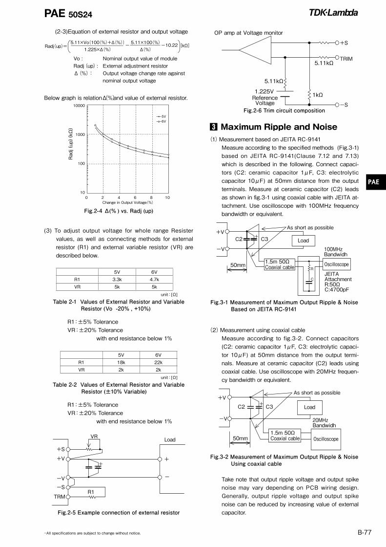
OP amp at Voltage monitor
+S
TRIM
-SFig.2-6 Trim circuit composition
3 Maximum Ripple and Noise(1)Measurement based on JEITA RC-9141 Measure according to the specified methods (Fig.3-1)
based on JEITA RC-9141(Clause 7.12 and 7.13) which is described in the following. Connect capaci-tors (C2: ceramic capacitor 1μF, C3: electrolytic capacitor 10μF) at 50mm distance from the output terminals. Measure at ceramic capacitor (C2) leads as shown in fig.3-1 using coaxial cable with JEITA at-tachment. Use oscilloscope with 100MHz frequency bandwidth or equivalent.
+V
-V
C2
50mm
+ C3
As short as possible
100MHzBandwidh
Load
Oscilloscope
JEITAAttachmentR:50ΩC:4700pF
Coaxial cable1.5m 50Ω
R
C
Fig.3-1 Measurement of Maximum Output Ripple & NoiseBased on JEITA RC-9141
(2)Measurement using coaxial cable Measure according to fig.3-2. Connect capacitors
(C2: ceramic capacitor 1μF, C3: electrolytic capaci-tor 10μF) at 50mm distance from the output termi-nals. Measure at ceramic capacitor (C2) leads using coaxial cable. Use oscilloscope with 20MHz frequen-cy bandwidth or equivalent.
+V
-V
C2 C3
50mm
+
As short as possible
20MHzBandwidh
Load
OscilloscopeCoaxial cable1.5m 50Ω
Fig.3-2 Measurement of Maximum Output Ripple & NoiseUsing coaxial cable
Take note that output ripple voltage and output spike noise may vary depending on PCB wiring design. Generally, output ripple voltage and output spike noise can be reduced by increasing value of external capacitor.

PAE 50S24
PAE
B-78 ・All specifications are subject to change without notice.
4 Maximum Line RegulationMaximum line regulation is the maximum value of output voltage change when input voltage is gradually varied within specified input voltage range. The measurement point for the input and output voltage are ±Vin and ±S (sense point) respectively
5 Maximum Load RegulationMaximum value of output voltage change when output current is gradually varied within specified output current range. The measurement point for the input and output voltage are ±Vin and ±S (sense point) respectively. When using at dynamic load mode, audible noise may be heard from the power module and output voltage fluctuation might in-crease
6 Over Current Protection (OCP)This power module has built-in OCP function.When output current exceed OCP set point, output voltage shut down and re-start automatically. Output will recover when short circuit or overload conditions are released. OCP setting value is fixed and therefore, can not be exter-nally adjusted.
7 Over Voltage Protection (OVP)This power module has built-in OVP function.OVP set point is relative to the rated output voltage value. When output voltage exceed OVP set point,output voltage shut down. OVP set point is fixed and therefore can not be changed. When OVP is triggered, output can be recovered by turn-ing input line off and then turning it on again after lowering the input voltage below the voltage value indicated below or by manual reset of the control ON/OFF terminal. Verifying OVP function shall be done by increasing output voltage with external resistor. For verifying OVP function, avoid applying external voltage to output terminal because this will cause power module damage.
Input voltage for OVP reset : 8VDC and below
8 Over Temperature Protection (OTP)This power module has built-in OTP function. This function operates and shuts down the output when temperature of the power module rises abnormally. Output voltage will re-start when PCB temperature drops down. Take note that OTP will operate again unless the cause of abnormal heat of the power module is eliminated.
9 Remote Sensing (+S,-S Terminal)Remote sensing terminal is provided to compensate for voltage drop across the wirings from the power module output terminal to the load input terminal. When remote sensing function is not used (local sensing), short +S terminal to +V terminal and, -S terminal to –V ter-minal.When using remote sensing function, output power of pow-er module should be within maximum output power. Also,
use within maximum output adjustable voltage at output terminal.When wire is long, Power Supply operation might be un-stable due to noise. Moreover, please do enough prior evaluation for remote sensing function by using shielded wire, twist pair, or parallel pattern.
Stabillize the output voltage at loadLoad
Twisted
+S
-S
+V ++
--V
+
Fig.9-1 Remote Sensing in Use
Stabillize the output voltage at loadLoad
+S
-S
+V +
--V
+
Fig.9-2 Remote Sensing Not in Use(Local Sensing)
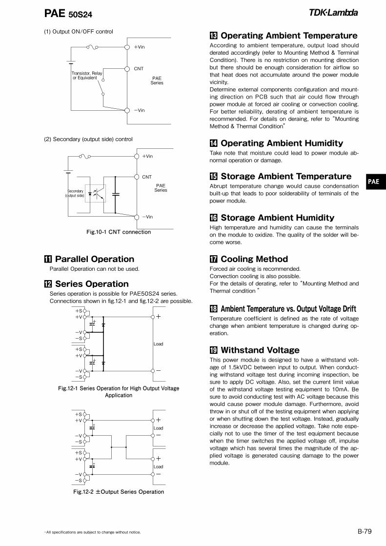
ON/OFF Control (CNT Terminal)Without turning the input supply on and off, the output can be enabled and disabled using this function.This function also can be used for output sequence of plu-ral modules.ON/OFF control circuit is on the primary side (the input side), CNT Terminal pin. For secondary control, isolation can be achieved through the use of an opto coupler or a relay.
CNT Terminal Level to -Vin Terminal Output StatusH Level (4V≦H≦35V) or Open OFFL Level (0V≦L≦0.8V) or Short ON
※ When control function is not used, CNT terminal is shorted to –Vin terminal.
※ When using long wiring, for prevention of noise, attach a 0.1μF capacitor between CNT Terminal and –Vin terminal.
※ At L level, maximum source current from CNT Terminal to –Vin terminal is 0.5mA.
※ The maximum CNT Terminal voltage when it is opened is 35V.
PAE
B-79・All specifications are subject to change without notice.
(1) Output ON/OFF control
+Vin
CNT
PAESeries
Transistor, Relay or Equivalent
-Vin
(2) Secondary (output side) control
+Vin
CNT
PAESeries
-Vin
Secondary(output side) Secondary(output side)
Fig.10-1 CNT connection
Parallel Operation Parallel Operation can not be used.
Series Operation Series operation is possible for PAE50S24 series. Connections shown in fig.12-1 and fig.12-2 are possible.
+S+V
+S+V
-V-S
-V-S
+
+
Load
+
-
Fig.12-1 Series Operation for High Output Voltage Application
+S+V
+S+V
-V-S
-V-S
+
+
Load
Load
+
+
-
-
Fig.12-2 ±Output Series Operation
Operating Ambient TemperatureAccording to ambient temperature, output load should derated accordingly (refer to Mounting Method & Terminal Condition). There is no restriction on mounting direction but there should be enough consideration for airflow so that heat does not accumulate around the power module vicinity. Determine external components configuration and mount-ing direction on PCB such that air could flow through power module at forced air cooling or convection cooling. For better reliability, derating of ambient temperature is recommended. For details on deraing, refer to “Mounting Method & Thermal Condition”
Operating Ambient HumidityTake note that moisture could lead to power module ab-normal operation or damage.
Storage Ambient TemperatureAbrupt temperature change would cause condensation built-up that leads to poor solderability of terminals of the power module.
Storage Ambient HumidityHigh temperature and humidity can cause the terminals on the module to oxidize. The quality of the solder will be-come worse.
Cooling MethodForced air cooling is recommended.Convection cooling is also possible.For the details of derating, refer to “Mounting Method and Thermal condition ”
Ambient Temperature vs. Output Voltage DriftTemperature coefficient is defined as the rate of voltage change when ambient temperature is changed during op-eration.
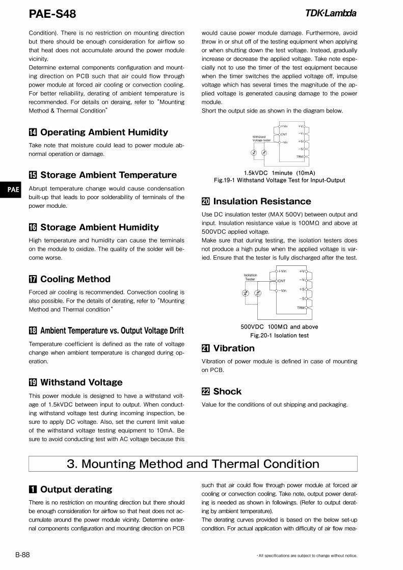
Withstand VoltageThis power module is designed to have a withstand volt-age of 1.5kVDC between input to output. When conduct-ing withstand voltage test during incoming inspection, be sure to apply DC voltage. Also, set the current limit value of the withstand voltage testing equipment to 10mA. Be sure to avoid conducting test with AC voltage because this would cause power module damage. Furthermore, avoid throw in or shut off of the testing equipment when applying or when shutting down the test voltage. Instead, gradually increase or decrease the applied voltage. Take note espe-cially not to use the timer of the test equipment because when the timer switches the applied voltage off, impulse voltage which has several times the magnitude of the ap-plied voltage is generated causing damage to the power module.
PAE 50S24
PAE 50S24
PAE
B-80 ・All specifications are subject to change without notice.
1 Output deratingThere is no restriction on mounting direction but there should be enough consideration for airflow so that heat does not ac-cumulate around the power module vicinity. Determine external components configuration and mounting direction on PCB such that air could flow through power module at forced air
cooling or convection cooling. Take note, output power derat-ing is needed as shown in followings. (Refer to output derat-ing by ambient temperature). The derating curves provided is based on the below set-up condition. For actual application with difficulty of air flow measurement, find of PCB temperature is recommended to ensure the power module operates within derating curve. (Refer to Output derating by PCB temperature)
3. Mounting Method and Thermal Condition
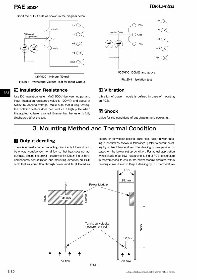
Short the output side as shown in the diagram below.
+Vin
WithstandVoltage tester
+V
-V
+S
-S
TRM
CNT
-Vin
1.5kVDC 1minute(10mA)
Fig.19-1 Withstand Voltage Test for Input-Output
Insulation ResistanceUse DC insulation tester (MAX 500V) between output and input. Insulation resistance value is 100MΩ and above at 500VDC applied voltage. Make sure that during testing, the isolation testers does not produce a high pulse when the applied voltage is varied. Ensure that the tester is fully discharged after the test.
+Vin
Isolation Tester
+V
-V
+S
-S
TRM
CNT
-Vin
500VDC 100MΩ and above
Fig.20-1 Isolation test
VibrationVibration of power module is defined in case of mounting on PCB.
ShockValue for the conditions of out shipping and packaging.
Power Module
Ta and air velocitymeasurement point
Air flow Air flow
12.7mm
76mm
25.4mm
PCB
Output
Input
Top View
CLL
Fig.1-1
PAE 50S24
PAE
B-81・All specifications are subject to change without notice.
(1)Output Derating by ambient temperature PAE50S24
Vin=24VDC
PAE50S24-5
10
8
6
4
2
0-40 -20 0 20 6040 80 100
Output Current (A)
Ambient temperature ()
Natural convection cooling (0.2m/s)1m/s
Air velocity
Fig.1-2
PAE50S24-6
8
6
4
2
0-40 -20 0 20 6040 80 100
自然空冷(0.2m/s)1m/s
風速Output Current (A)
Ambient temperature ()
Air velocityNatural convection cooling (0.2m/s)1m/s
Fig.1-3
(2) Output derating by PCB temperature When use with different measurement conditions from
output derating by ambient temperature, use output derating by PCB temperature as in Fig.1-5. PCB temperature is decided by temperature of the compo-nent surface in below Fig.1-4. Measurement of PCB temperature is recommended to ensure the module to operate within the derating curve.
+Vo+Vin
CNT
-Vin
+S
TRM
-S
-Vo
Measurement point of PCB temperature
Fig.1-4 Measurement point of PCB temperature
Output Derating by PCB temperaturePAE50S24
100
80
40
60
20
0-40 -20 0 20 6040 80 120100
Output load(%)
PCB temp crature()
基板温度による出力ディレーテイング
Fig.1-5 Output Dereting by PCB Temperature
2 Mounting Method(1) Prohibition area of pattern wiring Avoid wiring pattern on PCB in shaded area as
shown in Figure 2-1 as it may cause insulation prob-lem. Since the power module may influence by noise, care must be taken when wire the signal line on the non-shaded area.
+Vo+Vin
36.927.7
5.4
8.4
13.3
24.936.9
48.252.6
1.9
9.2
5.9-Vin
CNT
+S
TRM
-S
-Vo7.7
Fig.2-1 Prohibition area of wiring pattern
(2) Mounting hole on PCB Refer to below table for the diameter of hole and land
of PCB.
Type PAE_S24Input Terminal Pin φ1.0mm
Hole Diameter φ1.3mmLand Diameter φ2.6mm
Output Terminal Pin φ1.5mmHole Diameter φ1.8mmLand Diameter φ3.6mm
Signal Terminal Pin φ1.0mmHole Diameter φ1.3mmLand Diameter φ2.6mm
For position of the holes, see outline drawing of the power module.
(3) Recommended Material of PCB Recommended materials of the printed circuit board
is 4 layers glass epoxy with through holes.(thickness :t=1.6mm)
(4) Output Pattern Width When several to tens amperes of current flows to
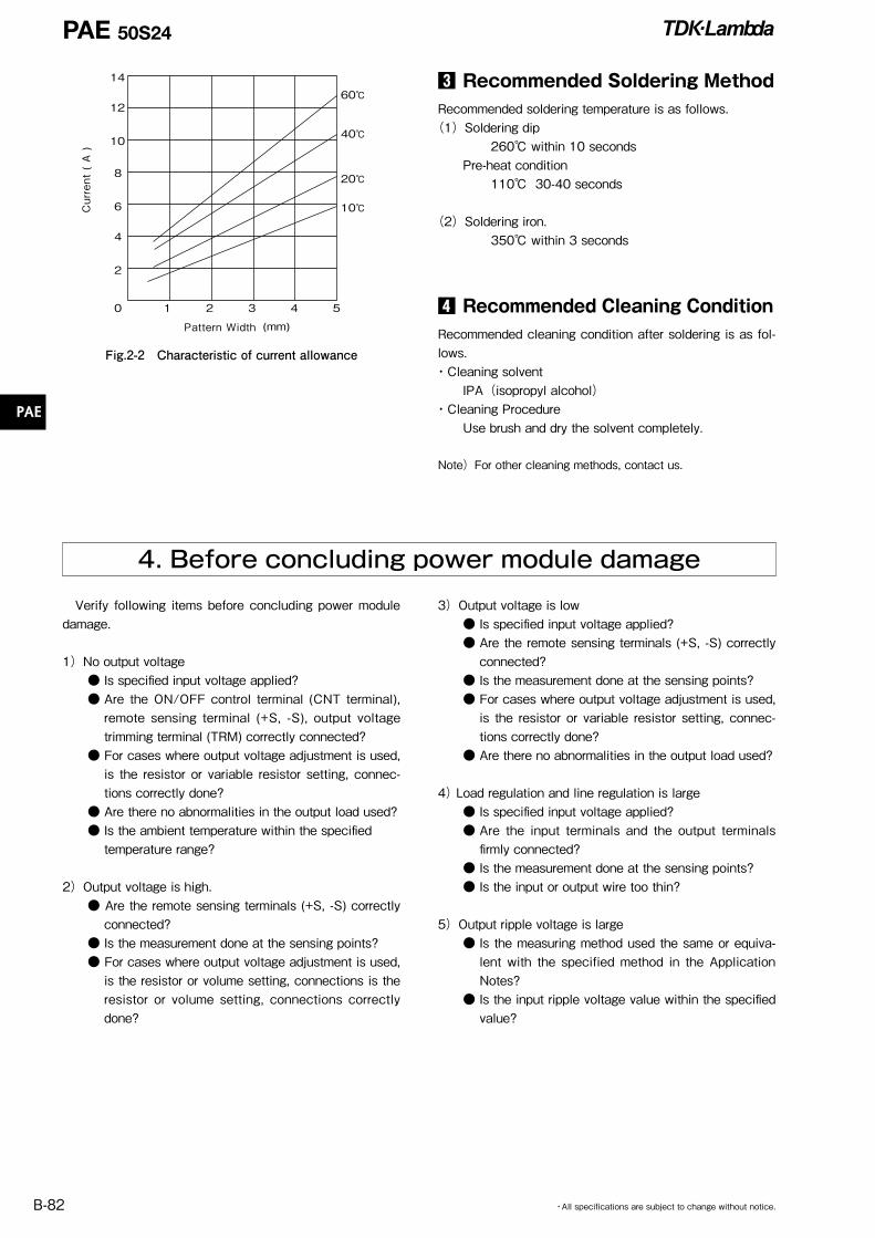
output pattern, voltage would drop and heat genera-tion would be higher for narrow pattern. Relationship between current and pattern width changes depend-ing on material of printed circuit board, thickness of conductor, temperature rise allowance. 35mm copper glass epoxy printed circuit board is shown in Fig-ure2-2 as an example.
For example, when 5A of current flows and tempera-ture rise below 10 are expected, pattern width shall be more than 4.2mm with 35µm copper plate (gener-ally 1mm/A is standard).
Confirmation is definitely necessary for designing be-cause characteristics shown in figure 2-2 depend on manufacturers of printed circuit board.
PAE 50S24
PAE
B-82 ・All specifications are subject to change without notice.
Verify following items before concluding power module damage.
1)No output voltage Is specified input voltage applied? Are the ON/OFF control terminal (CNT terminal),
remote sensing terminal (+S, -S), output voltage trimming terminal (TRM) correctly connected?
For cases where output voltage adjustment is used, is the resistor or variable resistor setting, connec-tions correctly done?
Are there no abnormalities in the output load used? Is the ambient temperature within the specified
temperature range?
2)Output voltage is high. Are the remote sensing terminals (+S, -S) correctly
connected? Is the measurement done at the sensing points? For cases where output voltage adjustment is used,
is the resistor or volume setting, connections is the resistor or volume setting, connections correctly done?
3)Output voltage is low Is specified input voltage applied? Are the remote sensing terminals (+S, -S) correctly
connected? Is the measurement done at the sensing points? For cases where output voltage adjustment is used,
is the resistor or variable resistor setting, connec-tions correctly done?
Are there no abnormalities in the output load used?
4) Load regulation and line regulation is large Is specified input voltage applied? Are the input terminals and the output terminals
firmly connected? Is the measurement done at the sensing points? Is the input or output wire too thin?
5)Output ripple voltage is large Is the measuring method used the same or equiva-
lent with the specified method in the Application Notes?
Is the input ripple voltage value within the specified value?
4. Before concluding power module damage
14
1260
40
20
10
10
8
6
4
2
0 1 2 3 4 5
(mm)Pattern Width
Current ( A )
Fig.2-2 Characteristic of current allowance
3 Recommended Soldering MethodRecommended soldering temperature is as follows.
(1)Soldering dip 260 within 10 seconds Pre-heat condition 110 30-40 seconds
(2)Soldering iron. 350 within 3 seconds
4 Recommended Cleaning ConditionRecommended cleaning condition after soldering is as fol-lows. ・Cleaning solvent IPA(isopropyl alcohol) ・Cleaning Procedure Use brush and dry the solvent completely.
Note)For other cleaning methods, contact us.

PAE-S48
PAE
B-83・All specifications are subject to change without notice.
PAE-S48 SERIES Instruction Manual
1. Terminal Explanation
Be sure to take note of precautions and warnings indicated in this manual when using this product. Improper usage may lead to electric shock or fire. Be sure to read this instruction manual thoroughly before using this product.
Caution
There are high voltage and high temperature components within this product. Refrain from disassembling this product or touching its internal components as this may lead to elec-tric shock or burned.
When the unit is operating, keep your hands and face away from the unit. You may get injured by accident.
Confirm connections to input/output terminals and signal ter-minals are correct as indicated in the instruction manual.
Attach a fast blow type external fuse to each module to ensure safety operation and compliance to each safety stan-dard approval.
This power module is designed for professional installation within the end user equipment.
Use isolated voltage by reinforced or double insulation as input power source.
Do not inject abnormal voltage to output terminal and signal terminal from the outside.
The injection of reverse voltage or over voltage exceeding nominal output voltage to output terminals might cause dam-age to internal circuit.
The application circuits and their parameter are for reference only. Be sure to verify effectiveness of application circuits and their parameters before finalizing circuit design.
The information in this document is subject to change with-out prior notice. For actual design-in, please refer to the lat-est publications of data sheet, etc., for the most up-to date specifications of the unit.
No part of this document may be copied or reproduced in any for, or by any mean without prior written consent of Den-sei-Lambda.
This product is not authorized for use as critical components in life support devices or systems without prior written con-sent of Densei-Lambda. As used herein:
1. Life support devices or systems are devices or systems which, (a) are intended for surgical implant into the body, or (b) support or sustain life, and whose failure to perform when properly used in accordance with instructions for use pro-vided in the labeling, can be reasonably expected to result in a significant injury to the user.
2. A critical component is any component of a life support de-vice or system whose failure to perform can be reasonably expected to cause the failure of the life support device or system, or to affect its safety or effectiveness.
Note:CE Marking
CE Marking, when applied to a product covered by instruction manual indicates compliance with the low voltage directive in that is complies with EN60950.
Before Using This Power Module
上 面
側 面
注1
注1. 型名・製造国名およびロットNo.が表示されます。注2. ターミナルピン 出力ピン: 2-φ1.5注3. ターミナルピン 入力・信号ピン: 6-φ1注4. 安全規格が表示されます。注5. オプションコード
型名
PAE50S48-**(標準モデル)
PAE50S48-**/V
過電圧保護OVP
出力遮断ON/OFFコントロールによるリセット方式または入力再投入の手動リセット可能
自動復帰型
注5注4
上面
下面
注2
注3
BottomView
-Vin -V-STRM+S+V+Vin
CNT
Input and Output Terminal Configrations (Bottom View)
[Input Terminal]−Vin : −Input TerminalCNT : ON/OFF Control Terminal+Vin : +Input Terminal
[Output Terminal]−V: −Output Terminal−S: −Remote Sensing TerminalTRM: Output Voltage Trimming Terminal+S: +Remote Sensing Terminal+V: +Output Terminal

PAE-S48
PAE
B-84 ・All specifications are subject to change without notice.
1 Input Voltage RangeInput Voltage Range for PAE_S48 Series is indicated be-low.
Input Voltage Range : 36 - 76VDC
Basically, ripple voltage (Vrpl) which results from rectifica-tion and filtering of commercial AC line might be included within the input voltage as shown in Fig.1-1. Ripple voltage must be limited within the voltage described below.
Allowable input ripple voltage : 2Vp-p
When this value is exceeded, the output ripple voltage might become large.Note that sudden input voltage change may cause varia-tion of output voltage transitionally.Also, input voltage waveform peak value must not exceed above input voltage range.
Input Voltage
Time
Input VoltageRangeVrpl
below 2V
t
Fig.1-1 Input Ripple Voltage
-Vin
+Vin
CNT
+S
+V
-V
-S
TRM
C1
Fuse
C2 C3
-
+
++
Load
50mm
Fig.1-2 Basic Connection
Input FusePAE_S48 Series module is not internally fused. To en-sure safe operation and to receive each Safety Standards approval, please connect an external fuse (fast-blow type) as shown in Fig.1-2.Fuse must be connected to the +Vin side if –Vin side is used as ground, or fuse must be connected to –Vin side if +Vin side is used as a ground.
Recommended input fuse current rating:PAE100S48 : 6.3APAE50S48 : 5A
C1 : Input capacitor C1 is recommended to stabilize the mod-ule when the module is powered from a high impedance source.Select the electrolytic capacitor with low ESR and suffi-cient allowable ripple current.
Verify actual ripple current value by actual measurement.
Recommended capacitor value : 33μF and above(Voltage rating : 100V and above)
Note)1. Use low impedance electrolytic capacitor with ex-cellent temperature characteristics.
(Nippon Chemicon LXV Series or equivalent)2. When input line inductance becomes excessively
high due to insertion of choke coil operation of the power module could become unstable. For this case, increase C1 value more than the value indicated above.
3. When ambient temperature becomes lower than −20 , connect ceramic capacitors.
C2, C3To reduce spike noise voltage at the output, connect 1μF ceramic capacitor and 10μF electrolytic capacitor or tan-talum capacitor between +V and –V within 50mm distance from the output terminals.Also, take note that output spike noise voltage could vary according to PCB wiring design.
Recommended capacitor value C2:1μF
C3:10μF
Maximum capacitance (ceramic capacitor) that can be connected between +V and –V, is shown below.
Maximum capacitance of output capacitor10,000μF (ALL Model)
C4:When switches or connectors are used between input source and PAE_S48 Series input terminals, impulse surge voltage is generated due to input throw-in by switch on/off or due to inserting/removing of power module from the active line. For this case, connect an additional elec-trolytic capacitor C4 as shown in fig.1-3 and fig.1-4.
Recommended capacitor value : 33μF and above(Voltage Rating : 100V and above)
Also, in-rush current flows at line throw-in.Therefore, be sure to verify capability of switch or fuse to withstand I2t at line throw-in.
Fuse
-Vin
+Vin
C1
+
C4
+
Switch
Fig.1-3 Input filter (C4) with Switch
2. Explanation on Specifications
PAE-S48
PAE
B-85・All specifications are subject to change without notice.
Fuse
-Vin
+Vin
C1+
C4
+
Switch
Fuse
C1
+
-Vin
+Vin
Fig.1-4 Input Filter with Switch when Plural PowerModules are connected
Reverse input connectionsReverse input polarity would cause module damage.For cases where reverse connections are possible, con-nect a protective diode and fuse. Use protective diode with higher voltage rating than the input voltage, and with higher surge current rating than the fuse.
Fuse
Load
+Vin
-Vin
+V
-V
Fig.1-5 Protection for Reversed Input Connection
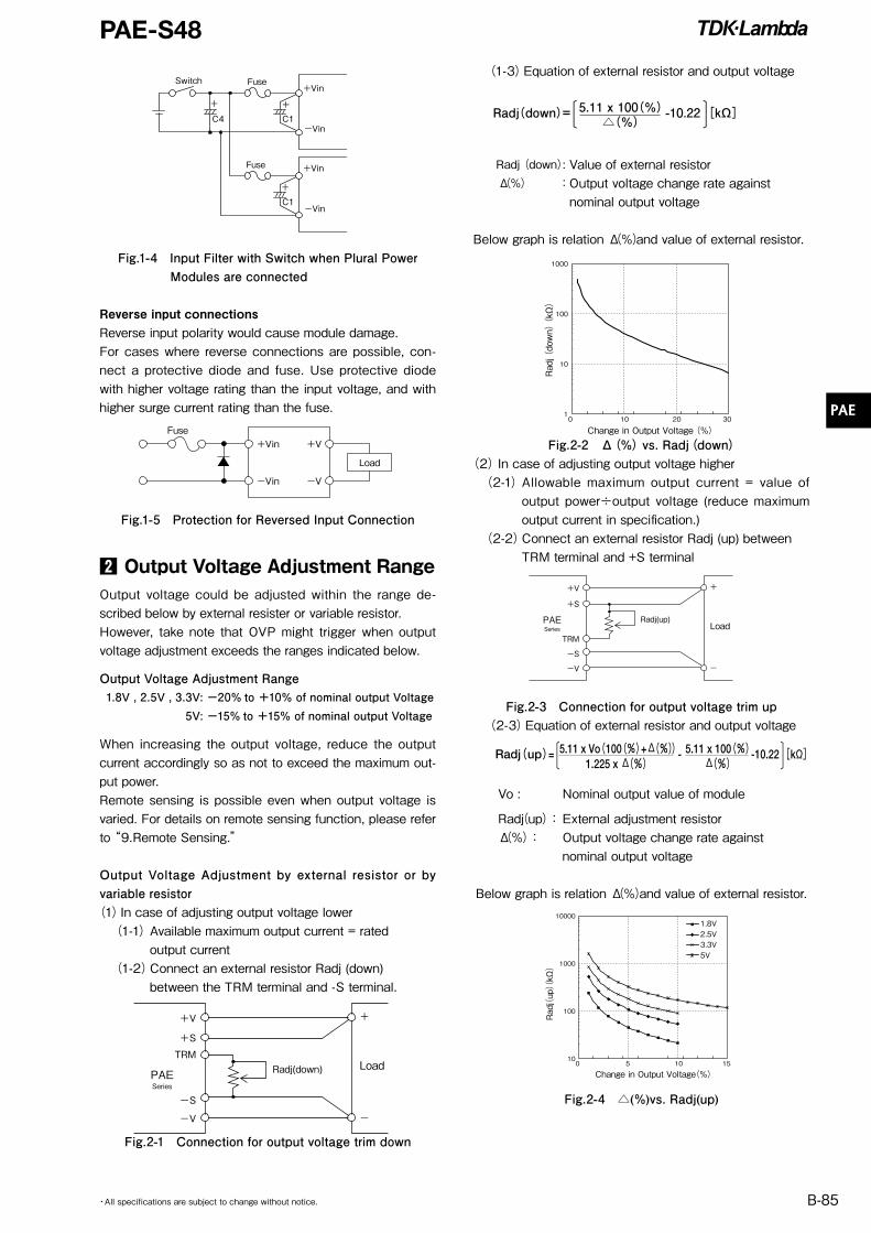
2 Output Voltage Adjustment RangeOutput voltage could be adjusted within the range de-scribed below by external resister or variable resistor. However, take note that OVP might trigger when output voltage adjustment exceeds the ranges indicated below.
Output Voltage Adjustment Range 1.8V , 2.5V , 3.3V: −20% to +10% of nominal output Voltage 5V: −15% to +15% of nominal output Voltage
When increasing the output voltage, reduce the output current accordingly so as not to exceed the maximum out-put power.Remote sensing is possible even when output voltage is varied. For details on remote sensing function, please refer to “9.Remote Sensing.”
Output Voltage Adjustment by external resistor or by variable resistor
(1)In case of adjusting output voltage lower(1-1) Available maximum output current = rated
output current(1-2)Connect an external resistor Radj (down)
between the TRM terminal and -S terminal.
LoadPAESeries
+
-
Radj(down)
-S
-V
+V
+S
TRM
Fig.2-1 Connection for output voltage trim down
(1-3)Equation of external resistor and output voltage
Radj(down)= 5.11 x 100(%)(%)
-10.22[kΩ]
Radj (down): Value of external resistor Δ(%) :Output voltage change rate against
nominal output voltage
Below graph is relation Δ(%)and value of external resistor.
1
10
100
1000
0 10 3020
Change in Output Voltage (%)
Radj (down) (kΩ)
Fig.2-2 Δ(%) vs. Radj(down)(2) In case of adjusting output voltage higher
(2-1) Allowable maximum output current = value of output power÷output voltage (reduce maximum output current in specification.)
(2-2)Connect an external resistor Radj (up) between TRM terminal and +S terminal
LoadPAESeries
+
-
Radj(up)
-S
-V
+V
+S
TRM
Fig.2-3 Connection for output voltage trim up(2-3)Equation of external resistor and output voltage
Radj(down)= 5.11 x 100(%)(%)
-10.22[kΩ]
Vo : Nominal output value of module
Radj(up): External adjustment resistor Δ(%): Output voltage change rate against
nominal output voltage
Below graph is relation Δ(%)and value of external resistor.
10
100
1000
100001.8V2.5V3.3V5V
0 5 1510
Change in Output Voltage(%)
Radj(up)(kΩ)
Fig.2-4 (%)vs. Radj(up)
PAE-S48
PAE
B-86 ・All specifications are subject to change without notice.
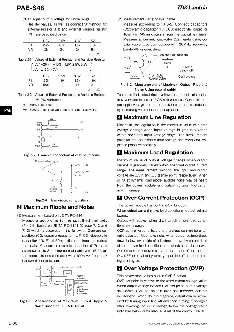
(3)To adjust output voltage for whole range Resister values, as well as connecting methods for external resistor (R1) and external variable resistor (VR) are described below.
1.8V 2.5V 3.3V 5V R1 2.2k 4.7k 10k 3.3k VR 2k 2k 2k 5k
unit:[Ω]
Table 2-1 Values of External Resistor and Variable Resistor Vo:−20% , +10% (1.8V, 2.5V, 3.3V) Vo:±15% (5V)
1.8V 2.5V 3.3V 5V R1 33k 18k 27k 18k VR 500 1k 1k 2k
unit:[Ω]
Table 2-2 Values of External Resistor and Variable Resistor(±10% Variable)
R1:±5% Tolerance VR:±20% Tolerance with end resistance below 1%
+S
+V
-S
TRM
-V
Load
+
-
VR
R1
+
Fig.2-5 Example connection of external resistor
-S
+S
TRIM
5.11kΩ
5.11kΩ
1.225V
OP amp at Voltage monitor
1kΩReferenceVoltage
Fig.2-6 Trim circuit composition
3 Maximum Ripple and Noise(1)Measurement based on JEITA RC-9141 Measure according to the specif ied methods
(Fig.3-1) based on JEITA RC-9141 (Clause 7.12 and 7.13) which is described in the following. Connect ca-pacitors (C2: ceramic capacitor 1μF, C3: electrolytic capacitor 10μF) at 50mm distance from the output terminals. Measure at ceramic capacitor (C2) leads as shown in fig.3-1 using coaxial cable with JEITA at-tachment. Use oscilloscope with 100MHz frequency bandwidth or equivalent.
-V
+V+
50mm
Load
As short as possible
Coaxial cable
100MHzBandwidh
JEITAAttachmentR:50ΩC:4700pF
C3C2
R
C
Oscilloscope1.5m 50Ω
Fig.3-1 Measurement of Maximum Output Ripple & Noise Based on JEITA RC-9141
(2)Measurement using coaxial cableMeasure according to fig.3-2. Connect capacitors (C2:ceramic capacitor 1μF, C3: electrolytic capacitor 10μF) at 50mm distance from the output terminals. Measure at ceramic capacitor (C2) leads using co-axial cable. Use oscilloscope with 20MHz frequency bandwidth or equivalent.
-V
+V+
50mm
Load
As short as possible
Coaxial Cable
20MHzbandwidth
C3C2
Oscilloscope1.5m 50Ω
Fig.3-2 Measurement of Maximum Output Ripple & Noise Using coaxial cable
Take note that output ripple voltage and output spike noise may vary depending on PCB wiring design. Generally, out-put ripple voltage and output spike noise can be reduced by increasing value of external capacitor.
4 Maximum Line RegulationMaximum line regulation is the maximum value of output voltage change when input voltage is gradually varied within specified input voltage range. The measurement point for the input and output voltage are ±Vin and ±S (sense point) respectively
5 Maximum Load RegulationMaximum value of output voltage change when output current is gradually varied within specified output current range. The measurement point for the input and output voltage are ±Vin and ±S (sense point) respectively. When using at dynamic load mode, audible noise may be heard from the power module and output voltage fluctuation might increase.
6 Over Current Protection (OCP)This power module has built-in OCP function.When output current is overload conditions, output voltage lowers.Output will recover when short circuit or overload condi-tions are released. OCP setting value is fixed and therefore, can not be exter-nally adjusted. Also, take note, when output voltage drops down below lower side of adjustment range by output short circuit or over load conditions, output might be shut down.Output can be recovered by manual reset of the control ON/OFF terminal or by turning input line off and then turn-ing it on again.
7 Over Voltage Protection (OVP)This power module has built-in OVP function.OVP set point is relative to the rated output voltage value. When output voltage exceed OVP set point, output voltage shut down. OVP set point is fixed and therefore can not be changed. When OVP is triggered, output can be recov-ered by turning input line off and then turning it on again after lowering the input voltage below the voltage value indicated below or by manual reset of the control ON/OFF
〔 〕
PAE-S48
PAE
B-87・All specifications are subject to change without notice.
terminal.Verifying OVP function shall be done by increasing output voltage with external resistor. For verifying OVP function, avoid applying external voltage to output terminal because this will cause power module damage.
Input voltage for OCP & OVP reset : 8VDC and below
/V Option (automatically recovery)The /V optional model will re-start with delay of 100ms ~300ms after shutdown by OCP & OVP triggering.When over current & over voltage are removed, output will recover normally.
8 Over Temperature Protection (OTP)This power module has built-in OTP function. This function operates and shuts down the output when temperature of the power module rises abnormally. Output voltage will re-start when PCB temperature drops down. Take note that OTP will operate again unless the cause of abnormal heat of the power module is eliminated.
9 Remote Sensing (+S, −S Terminal)Remote sensing terminal is provided to compensate for volt-age drop across the wirings from the power module output terminal to the load input terminal. When remote sensing function is not used (local sensing), short +S terminal to +V terminal and, -S terminal to –V terminal.When using remote sensing function, output power of power module should be within maximum output power. Also, use within maximum output adjustable voltage at output termi-nal.When wire is long, Power Supply operation might be unsta-ble due to noise. Moreover, please do enough prior evalua-tion for remote sensing function by using shielded wire, twist pair, or parallel pattern.
LoadStabillize the output voltage at load
+
Twisted
-V
-S
+V
-
+
+S
+
Fig.9-1 Remote Sensing in Use
Stabillize the output voltage at output loadLoad
+
-V
-S
+V
-
+
+S
Fig.9-2 Remote Sensing Not in Use(Local Sensing)
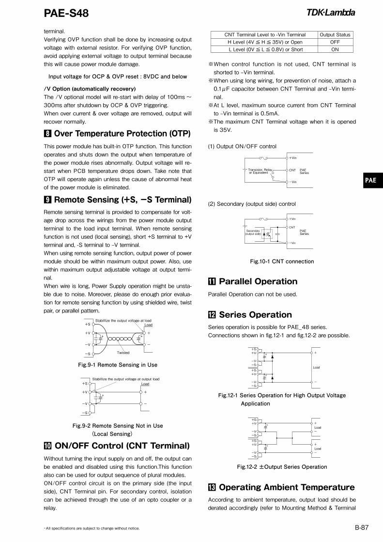
ON/OFF Control (CNT Terminal)Without turning the input supply on and off, the output can be enabled and disabled using this function.This function also can be used for output sequence of plural modules.ON/OFF control circuit is on the primary side (the input side), CNT Terminal pin. For secondary control, isolation can be achieved through the use of an opto coupler or a relay.
CNT Terminal Level to -Vin Terminal Output Status H Level (4V ≦ H ≦ 35V) or Open OFF L Level (0V ≦ L ≦ 0.8V) or Short ON
※When control function is not used, CNT terminal is shorted to –Vin terminal.
※When using long wiring, for prevention of noise, attach a 0.1μF capacitor between CNT Terminal and –Vin termi-nal.
※At L level, maximum source current from CNT Terminal to –Vin terminal is 0.5mA.
※The maximum CNT Terminal voltage when it is opened is 35V.
(1) Output ON/OFF control
PAESeries
Transistor, Relay or Equivalent
+Vin
CNT
-Vin
(2) Secondary (output side) control
PAESeries
Secondary(output side)
+Vin
CNT
-Vin
Fig.10-1 CNT connection
Parallel OperationParallel Operation can not be used.
Series OperationSeries operation is possible for PAE_48 series. Connections shown in fig.12-1 and fig.12-2 are possible.
Load
+
-
+
-S-V
+V+S
-S-V
+V+S
+
Fig.12-1 Series Operation for High Output Voltage Application
Load+
-
Load+
-
+
-S-V
+V+S
-S-V
+V+S
+
Fig.12-2 ±Output Series Operation
Operating Ambient TemperatureAccording to ambient temperature, output load should be derated accordingly (refer to Mounting Method & Terminal
PAE-S48
PAE
B-88 ・All specifications are subject to change without notice.
Condition). There is no restriction on mounting direction but there should be enough consideration for airflow so that heat does not accumulate around the power module vicinity. Determine external components configuration and mount-ing direction on PCB such that air could flow through power module at forced air cooling or convection cooling. For better reliability, derating of ambient temperature is recommended. For details on deraing, refer to “Mounting Method & Thermal Condition”
Operating Ambient HumidityTake note that moisture could lead to power module ab-normal operation or damage.
Storage Ambient TemperatureAbrupt temperature change would cause condensation built-up that leads to poor solderability of terminals of the power module.
Storage Ambient HumidityHigh temperature and humidity can cause the terminals on the module to oxidize. The quality of the solder will be-come worse.
Cooling MethodForced air cooling is recommended. Convection cooling is also possible. For the details of derating, refer to “Mounting Method and Thermal condition“
Ambient Temperature vs. Output Voltage DriftTemperature coefficient is defined as the rate of voltage change when ambient temperature is changed during op-eration.
Withstand VoltageThis power module is designed to have a withstand volt-age of 1.5kVDC between input to output. When conduct-ing withstand voltage test during incoming inspection, be sure to apply DC voltage. Also, set the current limit value of the withstand voltage testing equipment to 10mA. Be sure to avoid conducting test with AC voltage because this
would cause power module damage. Furthermore, avoid throw in or shut off of the testing equipment when applying or when shutting down the test voltage. Instead, gradually increase or decrease the applied voltage. Take note espe-cially not to use the timer of the test equipment because when the timer switches the applied voltage off, impulse voltage which has several times the magnitude of the ap-plied voltage is generated causing damage to the power module.Short the output side as shown in the diagram below.
Isolation Tester
-S
TRM
+S
-V
+V
-Vin
CNT
+Vin
WithstandVoltage tester
-S
TRM
+S
-V
+V
-Vin
CNT
+Vin
1.5kVDC 1minute (10mA)Fig.19-1 Withstand Voltage Test for Input-Output
Insulation ResistanceUse DC insulation tester (MAX 500V) between output and input. Insulation resistance value is 100MΩ and above at 500VDC applied voltage. Make sure that during testing, the isolation testers does not produce a high pulse when the applied voltage is var-ied. Ensure that the tester is fully discharged after the test.
Isolation Tester
-S
TRM
+S
-V
+V
-Vin
CNT
+Vin
WithstandVoltage tester
-S
TRM
+S
-V
+V
-Vin
CNT
+Vin
500VDC 100MΩ and above Fig.20-1 Isolation test
VibrationVibration of power module is defined in case of mounting on PCB.
ShockValue for the conditions of out shipping and packaging.
3. Mounting Method and Thermal Condition
1 Output deratingThere is no restriction on mounting direction but there should be enough consideration for airflow so that heat does not ac-cumulate around the power module vicinity. Determine exter-nal components configuration and mounting direction on PCB
such that air could flow through power module at forced air cooling or convection cooling. Take note, output power derat-ing is needed as shown in followings. (Refer to output derat-ing by ambient temperature).The derating curves provided is based on the below set-up condition. For actual application with difficulty of air flow mea-

PAE-S48
PAE
B-89・All specifications are subject to change without notice.
surement, find of PCB temperature is recommended to ensure the power module operates within derating curve. (Refer to output derating by PCB temperature)
Ta and air velocitymeasurement point
Top View
Air flow
Input
Output
12.7mm
25.4mm
PCB
Air flow
76mm
Power ModuleCL
Fig.1-1
(1)Output Derating by ambient temperature PAE100S48 (including /V option) Vin=48VDC
Air velocity
Air velocity
Ambient temperature ()
Natural convection cooling (0.2m/s)Output current (A)
-40 -20 0 20 40 60 80 100
5
10
15
20
0
PAE50S48-2R5
-40 -20 0 20 40 60 80 100
5
10
15
0
PAE50S48-3R3
-40 -20 0 20 40 60 80 100
2
4
6
8
10
0
PAE50S48-5
-40 -20 0 20 40 60 80 100
5
10
15
20
0
1m/s
2m/s
Ambient temperature ()
Natural convection cooling (0.2m/s)
Output current (A)
PAE50S48-1R8
-40 -20 0 20 40 60 80 100
5
15
10
20
25
0
PAE100S48-2R5
-40 -20 0 20 40 60 80 100
5
10
15
20
25
0
PAE100S48-3R3
-40 -20 0 20 40 60 80 100
5
10
15
20
0
PAE100S48-5
-40 -20 0 20 40 60 80 100
10
5
15
20
25
30
0
PAE100S48-1R8
-40 -20 0 20 40 60 80 100
10
5
15
20
25
30
0
PAE100S48-3R3/H
1m/s
2m/s
Air velocity
Ambient temperature ()
Natural convection cooling (0.2m/s)
Output current (A)
1m/s
2m/s
Air velocity
Ambient temperature ()
Natural convection cooling (0.2m/s)
Output current (A)
1m/s
2m/s
Air velocity
Ambient temperature ()
Natural convection cooling (0.2m/s)
Output current (A)
1m/s
2m/s
Air velocity
Ambient temperature ()
Natural convection cooling (0.2m/s)
Output current (A)
1m/s
2m/s
Air velocity
Ambient temperature ()
Natural convection cooling (0.2m/s)
Output current (A)
1m/s
2m/s
Air velocity
Ambient temperature ()
Natural convection cooling (0.2m/s)
Output current (A)
1m/s
2m/s
Air velocity
Ambient temperature ()
Natural convection cooling (0.2m/s)
Output current (A)
1m/s
2m/s
Fig.1-2
Air velocity
Air velocity
Ambient temperature ()
Natural convection cooling (0.2m/s)Output current (A)
-40 -20 0 20 40 60 80 100
5
10
15
20
0
PAE50S48-2R5
-40 -20 0 20 40 60 80 100
5
10
15
0
PAE50S48-3R3
-40 -20 0 20 40 60 80 100
2
4
6
8
10
0
PAE50S48-5
-40 -20 0 20 40 60 80 100
5
10
15
20
0
1m/s
2m/s
Ambient temperature ()
Natural convection cooling (0.2m/s)
Output current (A)
PAE50S48-1R8
-40 -20 0 20 40 60 80 100
5
15
10
20
25
0
PAE100S48-2R5
-40 -20 0 20 40 60 80 100
5
10
15
20
25
0
PAE100S48-3R3
-40 -20 0 20 40 60 80 100
5
10
15
20
0
PAE100S48-5
-40 -20 0 20 40 60 80 100
10
5
15
20
25
30
0
PAE100S48-1R8
-40 -20 0 20 40 60 80 100
10
5
15
20
25
30
0
PAE100S48-3R3/H
1m/s
2m/s
Air velocity
Ambient temperature ()
Natural convection cooling (0.2m/s)
Output current (A)
1m/s
2m/s
Air velocity
Ambient temperature ()
Natural convection cooling (0.2m/s)
Output current (A)
1m/s
2m/s
Air velocity
Ambient temperature ()
Natural convection cooling (0.2m/s)
Output current (A)
1m/s
2m/s
Air velocity
Ambient temperature ()
Natural convection cooling (0.2m/s)
Output current (A)
1m/s
2m/s
Air velocity
Ambient temperature ()
Natural convection cooling (0.2m/s)
Output current (A)
1m/s
2m/s
Air velocity
Ambient temperature ()
Natural convection cooling (0.2m/s)
Output current (A)
1m/s
2m/s
Air velocity
Ambient temperature ()
Natural convection cooling (0.2m/s)
Output current (A)
1m/s
2m/s
Fig.1-3
Air velocity
Air velocity
Ambient temperature ()
Natural convection cooling (0.2m/s)Output current (A)
-40 -20 0 20 40 60 80 100
5
10
15
20
0
PAE50S48-2R5
-40 -20 0 20 40 60 80 100
5
10
15
0
PAE50S48-3R3
-40 -20 0 20 40 60 80 100
2
4
6
8
10
0
PAE50S48-5
-40 -20 0 20 40 60 80 100
5
10
15
20
0
1m/s
2m/s
Ambient temperature ()
Natural convection cooling (0.2m/s)
Output current (A)
PAE50S48-1R8
-40 -20 0 20 40 60 80 100
5
15
10
20
25
0
PAE100S48-2R5
-40 -20 0 20 40 60 80 100
5
10
15
20
25
0
PAE100S48-3R3
-40 -20 0 20 40 60 80 100
5
10
15
20
0
PAE100S48-5
-40 -20 0 20 40 60 80 100
10
5
15
20
25
30
0
PAE100S48-1R8
-40 -20 0 20 40 60 80 100
10
5
15
20
25
30
0
PAE100S48-3R3/H
1m/s
2m/s
Air velocity
Ambient temperature ()
Natural convection cooling (0.2m/s)
Output current (A)
1m/s
2m/s
Air velocity
Ambient temperature ()
Natural convection cooling (0.2m/s)
Output current (A)
1m/s
2m/s
Air velocity
Ambient temperature ()
Natural convection cooling (0.2m/s)
Output current (A)
1m/s
2m/s
Air velocity
Ambient temperature ()
Natural convection cooling (0.2m/s)
Output current (A)
1m/s
2m/s
Air velocity
Ambient temperature ()
Natural convection cooling (0.2m/s)
Output current (A)
1m/s
2m/s
Air velocity
Ambient temperature ()
Natural convection cooling (0.2m/s)
Output current (A)
1m/s
2m/s
Air velocity
Ambient temperature ()
Natural convection cooling (0.2m/s)
Output current (A)
1m/s
2m/s
図 1-4
Air velocity
Air velocity
Ambient temperature ()
Natural convection cooling (0.2m/s)Output current (A)
-40 -20 0 20 40 60 80 100
5
10
15
20
0
PAE50S48-2R5
-40 -20 0 20 40 60 80 100
5
10
15
0
PAE50S48-3R3
-40 -20 0 20 40 60 80 100
2
4
6
8
10
0
PAE50S48-5
-40 -20 0 20 40 60 80 100
5
10
15
20
0
1m/s
2m/s
Ambient temperature ()
Natural convection cooling (0.2m/s)
Output current (A)
PAE50S48-1R8
-40 -20 0 20 40 60 80 100
5
15
10
20
25
0
PAE100S48-2R5
-40 -20 0 20 40 60 80 100
5
10
15
20
25
0
PAE100S48-3R3
-40 -20 0 20 40 60 80 100
5
10
15
20
0
PAE100S48-5
-40 -20 0 20 40 60 80 100
10
5
15
20
25
30
0
PAE100S48-1R8
-40 -20 0 20 40 60 80 100
10
5
15
20
25
30
0
PAE100S48-3R3/H
1m/s
2m/s
Air velocity
Ambient temperature ()
Natural convection cooling (0.2m/s)
Output current (A)
1m/s
2m/s
Air velocity
Ambient temperature ()
Natural convection cooling (0.2m/s)
Output current (A)
1m/s
2m/s
Air velocity
Ambient temperature ()
Natural convection cooling (0.2m/s)
Output current (A)
1m/s
2m/s
Air velocity
Ambient temperature ()
Natural convection cooling (0.2m/s)
Output current (A)
1m/s
2m/s
Air velocity
Ambient temperature ()
Natural convection cooling (0.2m/s)
Output current (A)
1m/s
2m/s
Air velocity
Ambient temperature ()
Natural convection cooling (0.2m/s)
Output current (A)
1m/s
2m/s
Air velocity
Ambient temperature ()
Natural convection cooling (0.2m/s)
Output current (A)
1m/s
2m/s
Fig.1-5
Air velocity
Air velocity
Ambient temperature ()
Natural convection cooling (0.2m/s)Output current (A)
-40 -20 0 20 40 60 80 100
5
10
15
20
0
PAE50S48-2R5
-40 -20 0 20 40 60 80 100
5
10
15
0
PAE50S48-3R3
-40 -20 0 20 40 60 80 100
2
4
6
8
10
0
PAE50S48-5
-40 -20 0 20 40 60 80 100
5
10
15
20
0
1m/s
2m/s
Ambient temperature ()
Natural convection cooling (0.2m/s)
Output current (A)
PAE50S48-1R8
-40 -20 0 20 40 60 80 100
5
15
10
20
25
0
PAE100S48-2R5
-40 -20 0 20 40 60 80 100
5
10
15
20
25
0
PAE100S48-3R3
-40 -20 0 20 40 60 80 100
5
10
15
20
0
PAE100S48-5
-40 -20 0 20 40 60 80 100
10
5
15
20
25
30
0
PAE100S48-1R8
-40 -20 0 20 40 60 80 100
10
5
15
20
25
30
0
PAE100S48-3R3/H
1m/s
2m/s
Air velocity
Ambient temperature ()
Natural convection cooling (0.2m/s)
Output current (A)
1m/s
2m/s
Air velocity
Ambient temperature ()
Natural convection cooling (0.2m/s)
Output current (A)
1m/s
2m/s
Air velocity
Ambient temperature ()
Natural convection cooling (0.2m/s)
Output current (A)
1m/s
2m/s
Air velocity
Ambient temperature ()
Natural convection cooling (0.2m/s)
Output current (A)
1m/s
2m/s
Air velocity
Ambient temperature ()
Natural convection cooling (0.2m/s)
Output current (A)
1m/s
2m/s
Air velocity
Ambient temperature ()
Natural convection cooling (0.2m/s)
Output current (A)
1m/s
2m/s
Air velocity
Ambient temperature ()
Natural convection cooling (0.2m/s)
Output current (A)
1m/s
2m/s
Fig.1-6
PAE50S48 (including /V option)Vin=48VDC
Air velocity
Air velocity
Ambient temperature ()
Natural convection cooling (0.2m/s)Output current (A)
-40 -20 0 20 40 60 80 100
5
10
15
20
0
PAE50S48-2R5
-40 -20 0 20 40 60 80 100
5
10
15
0
PAE50S48-3R3
-40 -20 0 20 40 60 80 100
2
4
6
8
10
0
PAE50S48-5
-40 -20 0 20 40 60 80 100
5
10
15
20
0
1m/s
2m/s
Ambient temperature ()
Natural convection cooling (0.2m/s)
Output current (A)
PAE50S48-1R8
-40 -20 0 20 40 60 80 100
5
15
10
20
25
0
PAE100S48-2R5
-40 -20 0 20 40 60 80 100
5
10
15
20
25
0
PAE100S48-3R3
-40 -20 0 20 40 60 80 100
5
10
15
20
0
PAE100S48-5
-40 -20 0 20 40 60 80 100
10
5
15
20
25
30
0
PAE100S48-1R8
-40 -20 0 20 40 60 80 100
10
5
15
20
25
30
0
PAE100S48-3R3/H
1m/s
2m/s
Air velocity
Ambient temperature ()
Natural convection cooling (0.2m/s)
Output current (A)
1m/s
2m/s
Air velocity
Ambient temperature ()
Natural convection cooling (0.2m/s)
Output current (A)
1m/s
2m/s
Air velocity
Ambient temperature ()
Natural convection cooling (0.2m/s)
Output current (A)
1m/s
2m/s
Air velocity
Ambient temperature ()
Natural convection cooling (0.2m/s)
Output current (A)
1m/s
2m/s
Air velocity
Ambient temperature ()
Natural convection cooling (0.2m/s)
Output current (A)
1m/s
2m/s
Air velocity
Ambient temperature ()
Natural convection cooling (0.2m/s)
Output current (A)
1m/s
2m/s
Air velocity
Ambient temperature ()
Natural convection cooling (0.2m/s)
Output current (A)
1m/s
2m/s
Fig.1-7
Air velocity
Air velocity
Ambient temperature ()
Natural convection cooling (0.2m/s)Output current (A)
-40 -20 0 20 40 60 80 100
5
10
15
20
0
PAE50S48-2R5
-40 -20 0 20 40 60 80 100
5
10
15
0
PAE50S48-3R3
-40 -20 0 20 40 60 80 100
2
4
6
8
10
0
PAE50S48-5
-40 -20 0 20 40 60 80 100
5
10
15
20
0
1m/s
2m/s
Ambient temperature ()
Natural convection cooling (0.2m/s)
Output current (A)
PAE50S48-1R8
-40 -20 0 20 40 60 80 100
5
15
10
20
25
0
PAE100S48-2R5
-40 -20 0 20 40 60 80 100
5
10
15
20
25
0
PAE100S48-3R3
-40 -20 0 20 40 60 80 100
5
10
15
20
0
PAE100S48-5
-40 -20 0 20 40 60 80 100
10
5
15
20
25
30
0
PAE100S48-1R8
-40 -20 0 20 40 60 80 100
10
5
15
20
25
30
0
PAE100S48-3R3/H
1m/s
2m/s
Air velocity
Ambient temperature ()
Natural convection cooling (0.2m/s)
Output current (A)
1m/s
2m/s
Air velocity
Ambient temperature ()
Natural convection cooling (0.2m/s)
Output current (A)
1m/s
2m/s
Air velocity
Ambient temperature ()
Natural convection cooling (0.2m/s)
Output current (A)
1m/s
2m/s
Air velocity
Ambient temperature ()
Natural convection cooling (0.2m/s)
Output current (A)
1m/s
2m/s
Air velocity
Ambient temperature ()
Natural convection cooling (0.2m/s)
Output current (A)
1m/s
2m/s
Air velocity
Ambient temperature ()
Natural convection cooling (0.2m/s)
Output current (A)
1m/s
2m/s
Air velocity
Ambient temperature ()
Natural convection cooling (0.2m/s)
Output current (A)
1m/s
2m/s
Fig.1-8
Air velocity
Air velocity
Ambient temperature ()
Natural convection cooling (0.2m/s)Output current (A)
-40 -20 0 20 40 60 80 100
5
10
15
20
0
PAE50S48-2R5
-40 -20 0 20 40 60 80 100
5
10
15
0
PAE50S48-3R3
-40 -20 0 20 40 60 80 100
2
4
6
8
10
0
PAE50S48-5
-40 -20 0 20 40 60 80 100
5
10
15
20
0
1m/s
2m/s
Ambient temperature ()
Natural convection cooling (0.2m/s)
Output current (A)
PAE50S48-1R8
-40 -20 0 20 40 60 80 100
5
15
10
20
25
0
PAE100S48-2R5
-40 -20 0 20 40 60 80 100
5
10
15
20
25
0
PAE100S48-3R3
-40 -20 0 20 40 60 80 100
5
10
15
20
0
PAE100S48-5
-40 -20 0 20 40 60 80 100
10
5
15
20
25
30
0
PAE100S48-1R8
-40 -20 0 20 40 60 80 100
10
5
15
20
25
30
0
PAE100S48-3R3/H
1m/s
2m/s
Air velocity
Ambient temperature ()
Natural convection cooling (0.2m/s)
Output current (A)
1m/s
2m/s
Air velocity
Ambient temperature ()
Natural convection cooling (0.2m/s)
Output current (A)
1m/s
2m/s
Air velocity
Ambient temperature ()
Natural convection cooling (0.2m/s)
Output current (A)
1m/s
2m/s
Air velocity
Ambient temperature ()
Natural convection cooling (0.2m/s)
Output current (A)
1m/s
2m/s
Air velocity
Ambient temperature ()
Natural convection cooling (0.2m/s)
Output current (A)
1m/s
2m/s
Air velocity
Ambient temperature ()
Natural convection cooling (0.2m/s)
Output current (A)
1m/s
2m/s
Air velocity
Ambient temperature ()
Natural convection cooling (0.2m/s)
Output current (A)
1m/s
2m/s
Fig.1-9
Air velocity
Air velocity
Ambient temperature ()
Natural convection cooling (0.2m/s)Output current (A)
-40 -20 0 20 40 60 80 100
5
10
15
20
0
PAE50S48-2R5
-40 -20 0 20 40 60 80 100
5
10
15
0
PAE50S48-3R3
-40 -20 0 20 40 60 80 100
2
4
6
8
10
0
PAE50S48-5
-40 -20 0 20 40 60 80 100
5
10
15
20
0
1m/s
2m/s
Ambient temperature ()
Natural convection cooling (0.2m/s)
Output current (A)
PAE50S48-1R8
-40 -20 0 20 40 60 80 100
5
15
10
20
25
0
PAE100S48-2R5
-40 -20 0 20 40 60 80 100
5
10
15
20
25
0
PAE100S48-3R3
-40 -20 0 20 40 60 80 100
5
10
15
20
0
PAE100S48-5
-40 -20 0 20 40 60 80 100
10
5
15
20
25
30
0
PAE100S48-1R8
-40 -20 0 20 40 60 80 100
10
5
15
20
25
30
0
PAE100S48-3R3/H
1m/s
2m/s
Air velocity
Ambient temperature ()
Natural convection cooling (0.2m/s)
Output current (A)
1m/s
2m/s
Air velocity
Ambient temperature ()
Natural convection cooling (0.2m/s)
Output current (A)
1m/s
2m/s
Air velocity
Ambient temperature ()
Natural convection cooling (0.2m/s)
Output current (A)
1m/s
2m/s
Air velocity
Ambient temperature ()
Natural convection cooling (0.2m/s)
Output current (A)
1m/s
2m/s
Air velocity
Ambient temperature ()
Natural convection cooling (0.2m/s)
Output current (A)
1m/s
2m/s
Air velocity
Ambient temperature ()
Natural convection cooling (0.2m/s)
Output current (A)
1m/s
2m/s
Air velocity
Ambient temperature ()
Natural convection cooling (0.2m/s)
Output current (A)
1m/s
2m/s
Fig.1-10
(2)Output derating by PCB temperatureWhen using with different measurement conditions from output derating by ambient temperature, use output derat-
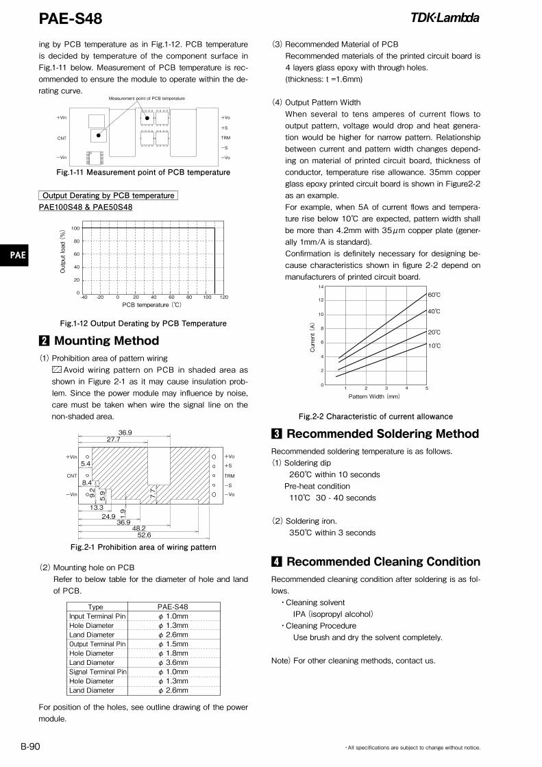
PAE-S48
PAE
B-90 ・All specifications are subject to change without notice.
ing by PCB temperature as in Fig.1-12. PCB temperature is decided by temperature of the component surface in Fig.1-11 below. Measurement of PCB temperature is rec-ommended to ensure the module to operate within the de-rating curve.
+Vin +Vo
Measurement point of PCB temperature
+S
-S
-Vo
TRM
-Vin
CNT
Fig.1-11 Measurement point of PCB temperature
Output Derating by PCB temperaturePAE100S48 & PAE50S48
Output load (%)
-40 -20 0 20 40 60 80 100 120
40
20
60
80
100
0
PCB temperature ()
Fig.1-12 Output Derating by PCB Temperature
2 Mounting Method(1)Prohibition area of pattern wiring Avoid wiring pattern on PCB in shaded area as
shown in Figure 2-1 as it may cause insulation prob-lem. Since the power module may influence by noise, care must be taken when wire the signal line on the non-shaded area.
36.927.7
5.4
8.4
13.324.9
36.948.252.6
9.2
5.9
1.9
7.7
+Vin +Vo
TRM
-S
-Vo
+S
CNT
-Vin
Fig.2-1 Prohibition area of wiring pattern
(2)Mounting hole on PCB Refer to below table for the diameter of hole and land
of PCB.
Type PAE-S48 Input Terminal Pin φ 1.0mm Hole Diameter φ 1.3mm Land Diameter φ 2.6mm Output Terminal Pin φ 1.5mm Hole Diameter φ 1.8mm Land Diameter φ 3.6mm Signal Terminal Pin φ 1.0mm Hole Diameter φ 1.3mm Land Diameter φ 2.6mm
For position of the holes, see outline drawing of the power module.
(3)Recommended Material of PCB Recommended materials of the printed circuit board is
4 layers glass epoxy with through holes. (thickness: t =1.6mm)
(4)Output Pattern Width When several to tens amperes of current flows to
output pattern, voltage would drop and heat genera-tion would be higher for narrow pattern. Relationship between current and pattern width changes depend-ing on material of printed circuit board, thickness of conductor, temperature rise allowance. 35mm copper glass epoxy printed circuit board is shown in Figure2-2 as an example.
For example, when 5A of current flows and tempera-ture rise below 10 are expected, pattern width shall be more than 4.2mm with 35μm copper plate (gener-ally 1mm/A is standard).
Confirmation is definitely necessary for designing be-cause characteristics shown in figure 2-2 depend on manufacturers of printed circuit board.
14
12
10
8
6
4
2
01 2 3 4 5
Pattern Width (mm)
60
40
20
10
Current (A)
Fig.2-2 Characteristic of current allowance
3 Recommended Soldering MethodRecommended soldering temperature is as follows.
(1)Soldering dip 260 within 10 seconds Pre-heat condition 110 30 - 40 seconds
(2)Soldering iron. 350 within 3 seconds
4 Recommended Cleaning ConditionRecommended cleaning condition after soldering is as fol-lows. ・Cleaning solvent
IPA(isopropyl alcohol) ・Cleaning Procedure
Use brush and dry the solvent completely.
Note)For other cleaning methods, contact us.
PAE-S48
PAE
B-91・All specifications are subject to change without notice.
4. Before concluding power module damage
Verify following items before concluding power module damage.1) No output voltage
Is specified input voltage applied? Are the ON/OFF control terminal (CNT terminal), re-
mote sensing terminal (+S, -S), output voltage trim-ming terminal (TRM) correctly connected?
For cases where output voltage adjustment is used, is the resistor or variable resistor setting, connec-tions correctly done?
Are there no abnormalities in the output load used? Is the ambient temperature within the specified tem-
perature range?
2) Output voltage is high. Are the remote sensing terminals (+S, -S) correctly
connected? Is the measurement done at the sensing points? For cases where output voltage adjustment is used,
is the resistor or volume setting, connections cor-rectly done?
3) Output voltage is low Is specified input voltage applied? Are the remote sensing terminals (+S, -S) correctly
connected? Is the measurement done at the sensing points? For cases where output voltage adjustment is used,
is the resistor or variable resistor setting, connec-tions correctly done?
Are there no abnormalities in the output load used?
4) Load regulation and line regulation is large Is specified input voltage applied? Are the input terminals and the output terminals
firmly connected? Is the measurement done at the sensing points? Is the input or output wire too thin?
5) Output ripple voltage is large Is the measuring method used the same or equiva-
lent with the specified method in the Application Notes?
Is the input ripple voltage value within the specified value?

B-92