Embed Size (px)
Citation preview
Power Application Controller
PAC5523 Data Sheet
Power Application Controller®
Multi-Mode Power ManagerTM
Configurable Analog Front EndTM
Application Specific Power DriversTM
ARM© Cortex®-M4F Controller Core
www.active-semi.com
Copyright © 2018 Active-Semi, Inc.
Power Application Controller
-2- Rev 1.0 – May 11, 2018
TABLE OF CONTENTS
1 PAC FAMILY APPLICATIONS ...........................................................................................10
2 PRODUCT SELECTION SUMMARY .................................................................................11
3 ORDERING INFORMATION ..............................................................................................12
4 FEATURES ........................................................................................................................13
4.1 Feature Overview........................................................................................................13
5 ABSOLUTE MAXIMUM RATINGS .....................................................................................15
6 ARCHITECTURAL BLOCK DIAGRAM ..............................................................................16
7 PIN CONFIGURATION ......................................................................................................17
7.1 PAC5523QM ...............................................................................................................17
8 PIN DESCRIPTION ...........................................................................................................18
9 MULTI-MODE POWER MANAGER (MMPM) ....................................................................23
9.1 Features .....................................................................................................................23
9.2 Functional Description ................................................................................................23
9.3 Multi-Mode Switching Supply (MMSS) Controller ........................................................24
9.4 Linear Regulators .......................................................................................................26
9.5 Power-up Sequence ...................................................................................................27
9.6 Hibernate Mode ..........................................................................................................27
9.7 Power and Temperature Monitor .................................................................................28
9.8 Voltage Reference ......................................................................................................28
9.9 Electrical Characteristics .............................................................................................29
9.10 Typical Performance Characteristics ...........................................................................32
10 CONFIGURABLE ANALOG FRONT END (CAFE) .........................................................33
10.1 Block Diagram ............................................................................................................33
10.2 Functional Description ................................................................................................34
10.3 Differential Programmable Gain Amplifier (DA) ...........................................................34
10.4 Single-Ended Programmable Gain Amplifier (AMP) ....................................................34
10.5 General Purpose Comparator (CMP) ..........................................................................34
Power Application Controller
-3- Rev 1.0 – May 11, 2018
10.6 Phase Comparator (PHC) ...........................................................................................35
10.7 Protection Comparator (PCMP) ..................................................................................35
10.8 Analog Output Buffer (BUF) ........................................................................................35
10.9 Analog Front End I/O (AIO) .........................................................................................35
10.10 Push Button (PBTN) ................................................................................................36
10.11 HP DAC and LP DAC ..............................................................................................36
10.12 ADC Pre-Multiplexer ................................................................................................36
10.13 Configurable Analog Signal Matrix (CASM) .............................................................36
10.14 Configurable Digital Signal Matrix (CDSM) ..............................................................37
10.15 Electrical Characteristics .........................................................................................38
10.16 Typical Performance Characteristics .......................................................................42
11 APPLICATION SPECIFIC POWER DRIVERS (ASPD) ..................................................43
11.1 Features .....................................................................................................................43
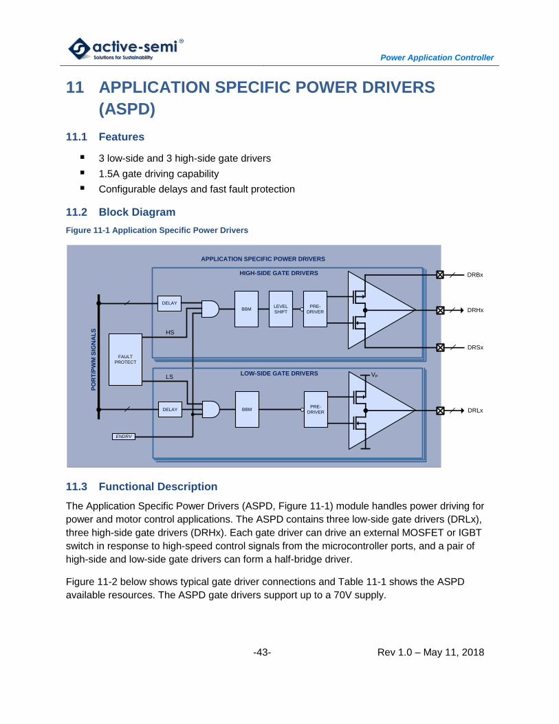
11.2 Block Diagram ............................................................................................................43
11.3 Functional Description ................................................................................................43
11.4 Low-Side Gate Driver ..................................................................................................44
11.5 High-Side Gate Driver .................................................................................................44
11.6 High-Side Switching Transients ..................................................................................45
11.7 Power Drivers Control .................................................................................................45
11.8 Gate Driver Fault Protection ........................................................................................46
11.9 Electrical Characteristics .............................................................................................46
11.10 Typical Performance Characteristics .......................................................................48
12 SOC CONTROL SIGNALS .............................................................................................50
12.1 High-side and Low-Side Gate Drivers .........................................................................50
12.2 SPI SOC Bus ..............................................................................................................52
12.3 ADC EMUX .................................................................................................................53
12.4 Analog Interrupts ........................................................................................................53
13 ADC/DTSE .....................................................................................................................54
13.1 ADC Block Diagram ....................................................................................................54
13.2 Functional Description ................................................................................................54
Power Application Controller
-4- Rev 1.0 – May 11, 2018
13.2.1 ADC .....................................................................................................................54
13.2.2 Dynamic Triggering and Sample Engine ..............................................................55
13.2.3 EMUX Control ......................................................................................................55
13.3 Electrical Characteristics .............................................................................................56
14 MEMORY SYSTEM........................................................................................................57
14.1 Features .....................................................................................................................57
14.2 Memory System Block Diagram ..................................................................................57
14.3 Functional Description ................................................................................................58
14.4 Program FLASH .........................................................................................................58
14.5 INFO FLASH ...............................................................................................................58
14.6 SRAM .........................................................................................................................58
14.7 Code Protection ..........................................................................................................59
14.8 Electrical Characteristics .............................................................................................60
15 SYSTEM AND CLOCK CONTROL .................................................................................61
15.1 Features .....................................................................................................................61
15.2 Block Diagram ............................................................................................................61
15.3 Clock Sources .............................................................................................................62
15.3.1 Ring Oscillator .....................................................................................................62
15.3.2 Reference Clock ..................................................................................................62
15.3.3 External Clock Input .............................................................................................62
15.4 PLL .............................................................................................................................62
15.5 Clock Tree ..................................................................................................................62
15.5.1 FRCLK .................................................................................................................63
15.5.2 SCLK ...................................................................................................................63
15.5.3 PCLK ...................................................................................................................63
15.5.4 ACLK ...................................................................................................................63
15.5.5 HCLK ...................................................................................................................63
15.6 Electrical Characteristics .............................................................................................64
16 ARM CORTEX-M4F MCU CORE ...................................................................................65
16.1 Features .....................................................................................................................65
Power Application Controller
-5- Rev 1.0 – May 11, 2018
16.2 Block Diagram ............................................................................................................65
16.3 Functional Description ................................................................................................66
16.4 Application Typical Current Consumption ...................................................................67
16.5 Electrical Characteristics .............................................................................................68
17 IO CONTROLLER ..........................................................................................................69
17.1 Features .....................................................................................................................69
17.2 Block Diagram ............................................................................................................69
17.3 Functional Description ................................................................................................70
17.4 Peripheral MUX ..........................................................................................................71
17.5 Electrical Characteristics .............................................................................................72
18 SERIAL INTERFACE .....................................................................................................73
18.1 Block Diagram ............................................................................................................73
18.2 Functional Description ................................................................................................74
18.3 I2C Controller ..............................................................................................................74
18.4 USART .......................................................................................................................74
18.4.1 USART SPI Mode ................................................................................................74
18.4.2 USART UART Mode ............................................................................................75
18.5 CAN ............................................................................................................................75
18.6 Dynamic Characteristics .............................................................................................76
19 PWM TIMERS ................................................................................................................79
19.1 Block Diagram ............................................................................................................79
19.2 Timer Features ...........................................................................................................80
19.2.1 CCR/PWM Timer .................................................................................................80
19.2.2 Dead-time Generators (DTG) ...............................................................................80
19.2.3 QEP Decoder.......................................................................................................81
20 GENERAL PURPOSE TIMERS .....................................................................................82
20.1 Block Diagram ............................................................................................................82
20.2 Functional Description ................................................................................................83
20.2.1 SOC Bus Watchdog Timer ...................................................................................83
20.2.2 Wake-up Timer ....................................................................................................83
Power Application Controller
-6- Rev 1.0 – May 11, 2018
20.2.3 Real-time Clock with Calendar (RTC) ..................................................................83
20.2.4 Windowed Watchdog Timer (WWDT) ..................................................................83
20.2.5 GP Timer (GPT) ...................................................................................................83
21 CRC ...............................................................................................................................84
21.1 Block Diagram ............................................................................................................84
21.2 Functional Description ................................................................................................84
22 THERMAL CHARACTERISTICS ....................................................................................85
23 APPLICATION EXAMPLES ............................................................................................86
24 PACKAGE OUTLINE AND DIMENSIONS ......................................................................87
25 LEGAL INFORMATION ..................................................................................................88
Power Application Controller
-7- Rev 1.0 – May 11, 2018
LIST OF FIGURES
Figure 1-1. PAC5523 Power Application Controller .................................................................... 9
Figure 1-1 Simplified Application Diagram .................................................................................10
Figure 6-1 Architectural Block Diagram .....................................................................................16
Figure 7-1 PAC5523QM Pin Configuration (TQFN66-48 Package) ...........................................17
Figure 8-1 Power Supply Bypass Capacitor Routing .................................................................22
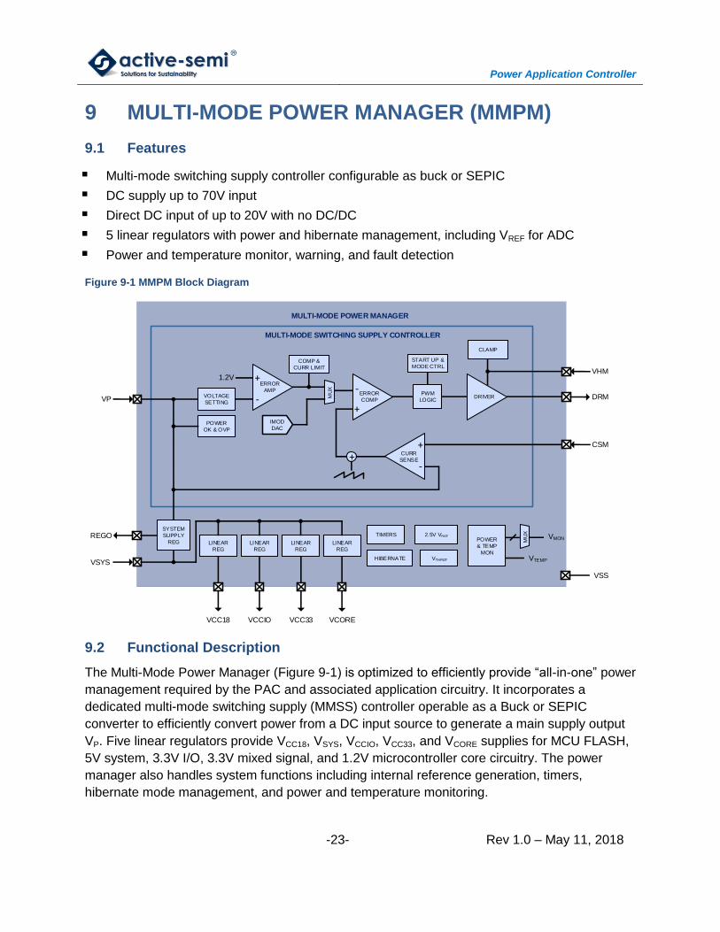
Figure 9-1 MMPM Block Diagram .............................................................................................23
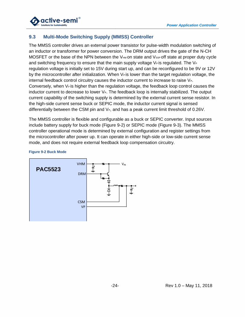
Figure 9-2 Buck Mode ...............................................................................................................24
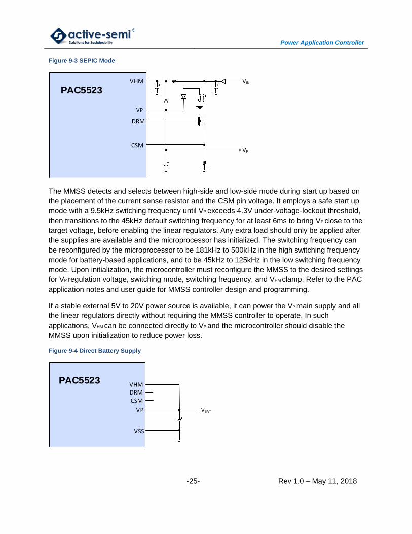
Figure 9-3 SEPIC Mode ............................................................................................................25
Figure 9-4 Direct Battery Supply ...............................................................................................25
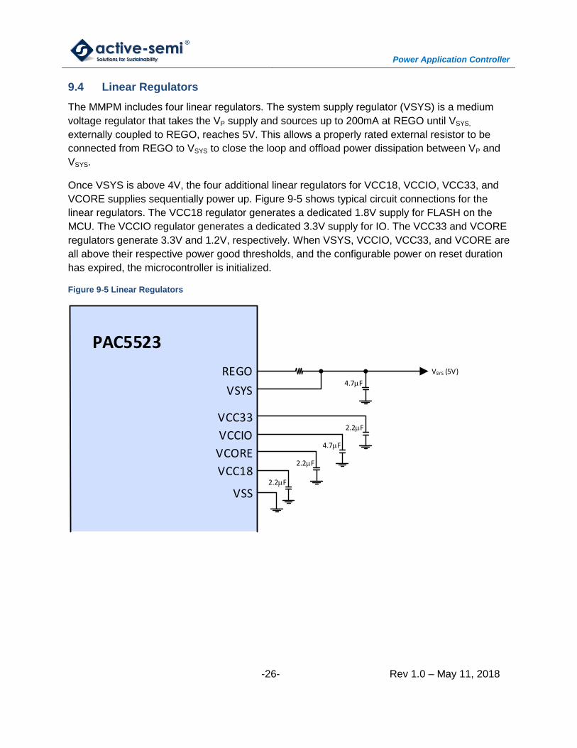
Figure 9-5 Linear Regulators .....................................................................................................26
Figure 9-6 Power-Up Sequence ................................................................................................27
Figure 10-1 Configurable Analog Front End ..............................................................................33
Figure 10-2 PGA Typical Performance Characteristics .............................................................42
Figure 11-1 Application Specific Power Drivers .........................................................................43
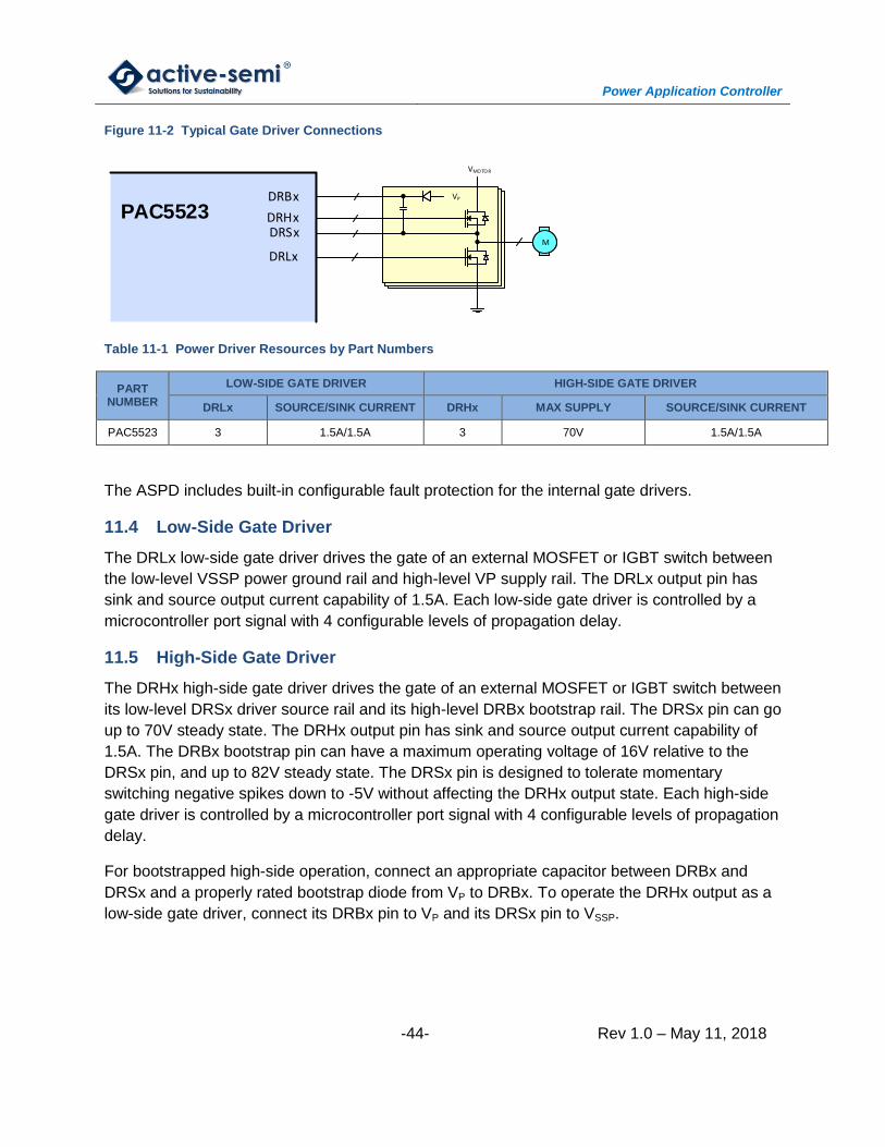
Figure 11-2 Typical Gate Driver Connections ...........................................................................44
Figure 11-3 High-Side Switching Transients and Optional Circuitry ...........................................45
Figure 11-4 ASPD Gate Driver Typical Performance Characteristics ........................................48
Figure 11-5 ASPD Gate Driver Typical Performance Characteristics (cont) ..............................49
Figure 12-1 SOC Signals for Gate Drivers ................................................................................50
Figure 13-1 ADC with DTSE .....................................................................................................54
Figure 14-1 Memory System .....................................................................................................57
Figure 15-1 Clock Control System .............................................................................................61
Figure 16-1 ARM Cortex-M4F Microcontroller Core ..................................................................65
Figure 17-1 IO Controller Block Diagram...................................................................................69
Figure 18-1 Serial Interface Block Diagram ...............................................................................73
Figure 18-2 I2C Timing Diagram ................................................................................................77
Figure 19-1 PWM Timers Block Diagram ..................................................................................79
Figure 20-1 SOC Bus Watchdog and Wake-up Timer ...............................................................82
Figure 20-2 General Purpose Timers ........................................................................................82
Figure 21-1 CRC Block Diagram ...............................................................................................84
Figure 23-1 Sensorless FOC/BEMF Motor Drive Using PAC5523 (Simplified Diagram) ............86
Figure 24-1 TQFN66-48 Package Outline and Dimensions .......................................................87
Power Application Controller
-8- Rev 1.0 – May 11, 2018
LIST OF TABLES
Table 2-1 Product Selection Summary ......................................................................................11
Table 3-1 Ordering Information .................................................................................................12
Table 5-1 Absolute Maximum Ratings .......................................................................................15
Table 8-1 Multi-Mode Power Manager (MMPM) and System Pin Description ...........................18
Table 8-2 Configurable Analog Front End (CAFE) Pin Description ............................................19
Table 8-3 Application Specific Power Drivers (ASPD) Pin Description ......................................20
Table 8-4 I/O Ports Pin Description ...........................................................................................21
Table 9-1 Multi-Mode Switching Supply Controller Electrical Characteristics ............................29
Table 9-2 Linear Regulators Electrical Characteristics ..............................................................30
Table 9-3. Power System Electrical Characteristics ..................................................................30
Table 10-1 Differential Programmable Gain Amplifier (DA) Electrical Characteristics ................38
Table 10-2 Single-Ended Programmable Gain Amplifier (AMP) Electrical Characteristics .........38
Table 10-3 General Purpose Comparator (CMP) Electrical Characteristics ...............................39
Table 10-4 Phase Comparator (PHC) Electrical Characteristics ................................................39
Table 10-5 Protection Comparator (PCMP) Electrical Characteristics .......................................39
Table 10-6 Analog Output Buffer (BUF) Electrical Characteristics .............................................40
Table 10-7 Analog Front End (AIO) Electrical Characteristics ...................................................40
Table 10-8 Push Button (PBTN) Electrical Characteristics ........................................................40
Table 10-9 HP DAC and LP DAC Electrical Characteristics ......................................................41
Table 11-1 Power Driver Resources by Part Numbers .............................................................44
Table 11-2 Power Driver Delay Configuration ...........................................................................45
Table 11-3 Gate Driver Electrical Characteristics ......................................................................46
Table 12-1 PWM to ASPD Gate Driver Options (DTG Enabled) ................................................51
Table 12-2 PWM to ASPD Gate Driver Options (DTG Disabled) ...............................................51
Table 12-3 SPI SOC Bus Connections ......................................................................................52
Table 12-4 SPI SOC Bus Connections ......................................................................................53
Table 12-5 Analog Interrupts .....................................................................................................53
Table 13-1 ADC and DTSE Electrical Characteristics ...............................................................56
Table 14-1 Code Protection Level Description ..........................................................................59
Table 14-2 Memory System Electrical Characteristics...............................................................60
Table 15-1 CCS Electrical Characteristics .................................................................................64
Table 16-1 PAC55XX Application Typical Current Consumption ...............................................67
Table 16-2 MCU and Clock Control System Electrical Characteristics ......................................68
Table 17-1 PAC5523 Peripheral Pin MUX .................................................................................71
Table 17-2 IO Controller Electrical Characteristics ....................................................................72
Table 18-1 Serial Interface Dynamic Characteristics .................................................................76
Table 18-2 I2C Dynamic Characteristics ....................................................................................76
Table 22-1 Thermal Characteristics ..........................................................................................85
Power Application Controller
-9- Rev 1.0 – May 11, 2018
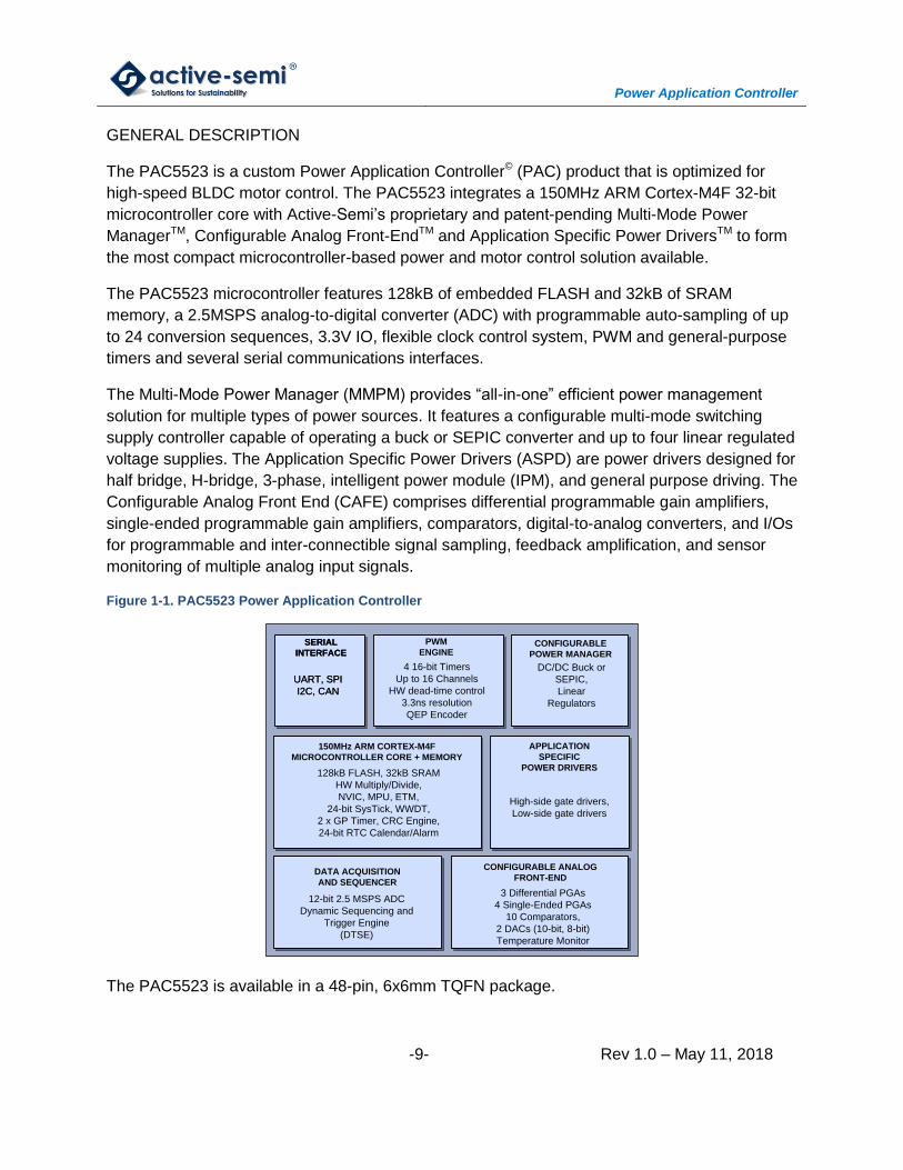
GENERAL DESCRIPTION
The PAC5523 is a custom Power Application Controller© (PAC) product that is optimized for
high-speed BLDC motor control. The PAC5523 integrates a 150MHz ARM Cortex-M4F 32-bit
microcontroller core with Active-Semi’s proprietary and patent-pending Multi-Mode Power
ManagerTM, Configurable Analog Front-EndTM and Application Specific Power DriversTM to form
the most compact microcontroller-based power and motor control solution available.
The PAC5523 microcontroller features 128kB of embedded FLASH and 32kB of SRAM
memory, a 2.5MSPS analog-to-digital converter (ADC) with programmable auto-sampling of up
to 24 conversion sequences, 3.3V IO, flexible clock control system, PWM and general-purpose
timers and several serial communications interfaces.
The Multi-Mode Power Manager (MMPM) provides “all-in-one” efficient power management
solution for multiple types of power sources. It features a configurable multi-mode switching
supply controller capable of operating a buck or SEPIC converter and up to four linear regulated
voltage supplies. The Application Specific Power Drivers (ASPD) are power drivers designed for
half bridge, H-bridge, 3-phase, intelligent power module (IPM), and general purpose driving. The
Configurable Analog Front End (CAFE) comprises differential programmable gain amplifiers,
single-ended programmable gain amplifiers, comparators, digital-to-analog converters, and I/Os
for programmable and inter-connectible signal sampling, feedback amplification, and sensor
monitoring of multiple analog input signals.
Figure 1-1. PAC5523 Power Application Controller
PWM
ENGINE
4 16-bit Timers
Up to 16 Channels
HW dead-time control
3.3ns resolution
QEP Encoder
CONFIGURABLE
POWER MANAGER
DC/DC Buck or
SEPIC,
Linear
Regulators
SERIAL
INTERFACE
UART, SPI
I2C, CAN
SERIAL
INTERFACE
UART, SPI
I2C, CAN
150MHz ARM CORTEX-M4F
MICROCONTROLLER CORE + MEMORY
128kB FLASH, 32kB SRAM
HW Multiply/Divide,
NVIC, MPU, ETM,
24-bit SysTick, WWDT,
2 x GP Timer, CRC Engine,
24-bit RTC Calendar/Alarm
APPLICATION
SPECIFIC
POWER DRIVERS
High-side gate drivers,
Low-side gate drivers
CONFIGURABLE ANALOG
FRONT-END
3 Differential PGAs
4 Single-Ended PGAs
10 Comparators,
2 DACs (10-bit, 8-bit)
Temperature Monitor
DATA ACQUISITION
AND SEQUENCER
12-bit 2.5 MSPS ADC
Dynamic Sequencing and
Trigger Engine
(DTSE)
The PAC5523 is available in a 48-pin, 6x6mm TQFN package.
Power Application Controller
-10- Rev 1.0 – May 11, 2018
1 PAC FAMILY APPLICATIONS
General-purpose high-voltage system controllers
Home appliances
Ceiling Fans
Standing Fans
Compressors
Power Tools
Garden Tools
Motor Controllers
Industrial Applications
Drone/RC
Figure 1-1 Simplified Application Diagram
PWM
ENGINE
MULTI-MODE
POWER
MANAGER
SERIAL
INTERFACE
SERIAL
INTERFACE
150MHz ARM CORTEX-M0
MICROCONTROLLER CORE &
MEMORY
APPLICATION
SPECIFIC
POWER
DRIVERS
CONFIGURABLE ANALOG
FRONT-END
DATA
ACQUISITION
AND DTSE
PAC5523
UART/SPI/CAN/I2C
MONITORINGSIGNALS
BUCK/SEPIC
MM
Power Application Controller
-11- Rev 1.0 – May 11, 2018
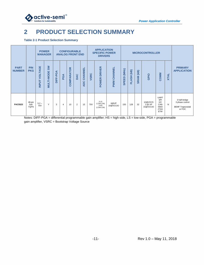
2 PRODUCT SELECTION SUMMARY
Table 2-1 Product Selection Summary
PART NUMBER
PIN PKG
POWER MANAGER
CONFIGURABLE ANALOG FRONT END
APPLICATION SPECIFIC POWER
DRIVERS MICROCONTROLLER
PRIMARY APPLICATION
INP
UT
VO
LT
AG
E
MU
LT
I-M
OD
E S
W
DIF
F-P
GA
PG
A
CO
MP
AR
AT
OR
DA
C
AD
C C
HA
NN
EL
VS
RC
PO
WE
R D
RIV
ER
PW
M C
HA
NN
EL
SP
EE
D (
MH
z)
FL
AS
H (
kB
)
SR
AM
(kB
)
GP
IO
CO
MM
XT
AL
PAC5523 48-pin
6x6 TQFN
5.2 – 70V
Y 3 4 10 2 15 70V
3 LS (1.5A/1.5A)
3 HS (1.5A/1.5A)
6@VP 15@VCCIO
150 128 32 10@VSYS
3 @ VP 15@VCCIO
UART SPI I2C
CAN SWD JTAG ETM
N
3 half-bridge 3 phase control
BEMF Trapezoidal
or FOC
Notes: DIFF-PGA = differential programmable gain amplifier; HS = high-side, LS = low-side, PGA = programmable
gain amplifier, VSRC = Bootstrap Voltage Source
Power Application Controller
-12- Rev 1.0 – May 11, 2018
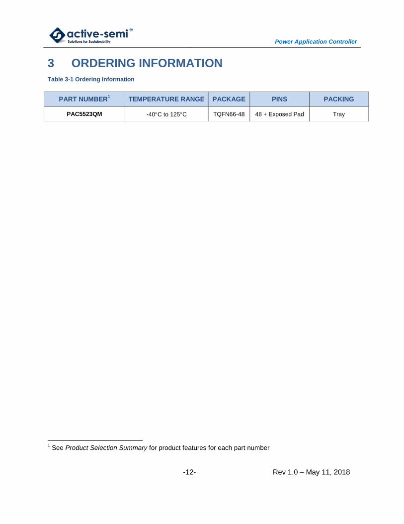
3 ORDERING INFORMATION
Table 3-1 Ordering Information
1 See Product Selection Summary for product features for each part number
PART NUMBER1 TEMPERATURE RANGE PACKAGE PINS PACKING
PAC5523QM -40C to 125C TQFN66-48 48 + Exposed Pad Tray
Power Application Controller
-13- Rev 1.0 – May 11, 2018
4 FEATURES
4.1 Feature Overview
Proprietary Multi-Mode Power Manager
o Multi-mode switching supply controller configurable for DC/DC Buck or SEPIC topologies
o Direct battery supply from 5V – 20V
o 4 Linear regulators with power and hibernate management
o Power and temperature monitor, warning, fault detection
Proprietary Configurable Analog Front-End
o 10 Analog Front-End IO pins
o 3 Differential Programmable Gain Amplifiers
o 4 Single-ended Programmable Gain Amplifiers
o Programmable Over-Current Protection
o 10 Comparators
o 2 DACs (10-bit and 8-bit)
o Integrated BEMF comparator mode with virtual center-tap
Proprietary Application Specific Power Drivers
o 3 Low-side and 3 High-Side gate drivers with 1.5A gate driving capacity
o Configurable propagation delay and fault protection
150MHz ARM Cortex-M4F 32-bit Microcontroller Core
o Single-cycle 32-bit x 32-bit hardware multiplier
o 32-bit hardware divider
o DSP Instructions and Saturation Arithmetic Support
o Integrated sleep and deep sleep modes
o Single-precision Floating Point Unit (FPU)
o 8-region Memory Protection Unit (MPU)
o Nested Vectored Interrupt Controller (NVIC) with 32 Interrupts with 8 levels of priority
o 24-Bit SysTick Timer
o Wake-up Interrupt Controller (WIC) allowing power-saving sleep modes
o Clock-gating allowing low-power operation
o Embedded Trace Macrocell (ETM) for in-system debugging at real-time without
breakpoints
Memory
o 128kB FLASH
o 32kB SRAM with ECC
o 2 x 1kB INFO FLASH area for manufacturing information
o 1 x 1kB INFO FLASH area for user parameter storage and application configuration or
code
o Code Protection
Power Application Controller
-14- Rev 1.0 – May 11, 2018
Analog to Digital Converter (ADC)
o 12-bit resolution
o 2.5MSPS
o Programmable Dynamic Triggering and Sampling Engine (DTSE)
I/O
o 3.3V Digital Input/Output or Analog Input for ADC
o Configurable weak pull-up and pull-down
o Configurable drive strength (6mA to 25mA minimum)
o Dedicated Integrated IO power supply (3.3V)
o Flexible peripheral MUX allowing each IO pin to be configured with one of up to 8
peripheral functions
o Flexible Interrupt Controller
Flexible Clock Control System (CCS)
o 300MHz PLL from internal 2% oscillator
o 20MHz Ring Oscillator
o 20MHz External Clock Input
Timing Generators
o Four 16-bit timers with up to 32 PWM/CC blocks
16 Programmable Hardware Dead-time generators
Up to 300MHz input clock for high-resolution PWM
o 16-bit Windowed Watchdog Timer (WWDT)
o 24-bit Real-time Clock (RTC) with Calendar and Alarm Functions
o 24-bit SysTick Timer
o 2 x 24-bit General-purpose count-down timers with interrupt
o Wake-up timer for sleep modes from 0.125s to 8s
Communication Peripherals
o 3 x USART
SPI or UART modes
SPI Master/Slave, up to 25MHz
UART, up to 1Mbps
o I2C Master/Slave
o CAN 2.0A/B Controller
o Single Wire Debugger (SWD)/JTAG
o Embedded Trace Macrocell (ETM)
4-Level User-Configurable Code Protection
96-bit Unique ID
CRC Engine
o Offloads software for communications and safety protocol through hardware acceleration
o Configurable Polynomial (CRC-16 or CRC-8)
o Configurable Input Data Width, Input and Output Reflection
o Programmable Seed Value
Power Application Controller
-15- Rev 1.0 – May 11, 2018
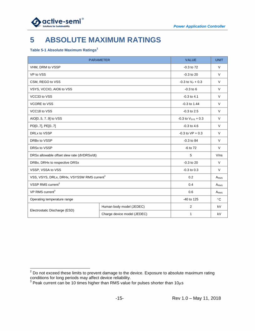
5 ABSOLUTE MAXIMUM RATINGS
Table 5-1 Absolute Maximum Ratings2
PARAMETER VALUE UNIT
VHM, DRM to VSSP -0.3 to 72 V
VP to VSS -0.3 to 20 V
CSM, REGO to VSS -0.3 to VP + 0.3 V
VSYS, VCCIO, AIO6 to VSS -0.3 to 6 V
VCC33 to VSS -0.3 to 4.1 V
VCORE to VSS -0.3 to 1.44 V
VCC18 to VSS -0.3 to 2.5 V
AIO[0..5, 7..9] to VSS -0.3 to VSYS + 0.3 V
PD[0..7], PE[0..7] -0.3 to 4.6 V
DRLx to VSSP -0.3 to VP + 0.3 V
DRBx to VSSP -0.3 to 84 V
DRSx to VSSP -6 to 72 V
DRSx allowable offset slew rate (dVDRSx/dt) 5 V/ns
DRBx, DRHx to respective DRSx -0.3 to 20 V
VSSP, VSSA to VSS -0.3 to 0.3 V
VSS, VSYS, DRLx, DRHx, VSYSSW RMS current3 0.2 ARMS
VSSP RMS current3 0.4 ARMS
VP RMS current3 0.6 ARMS
Operating temperature range -40 to 125 C
Electrostatic Discharge (ESD) Human body model (JEDEC) 2 kV
Charge device model (JEDEC) 1 kV
2 Do not exceed these limits to prevent damage to the device. Exposure to absolute maximum rating
conditions for long periods may affect device reliability. 3 Peak current can be 10 times higher than RMS value for pulses shorter than 10s
Power Application Controller
-16- Rev 1.0 – May 11, 2018
6 ARCHITECTURAL BLOCK DIAGRAM
Figure 6-1 Architectural Block Diagram
IO
128kB FLASH
32kB SRAM
CLOCK
CONTROL
RTC/Calendar
GPIO
USART (3)
I2C
CAN
SYSTEM
CONTROL
AP
B/A
HB
PAC5523
Power Application Controller
PX.Y
DEBUG/
ETM
ARM
CORTEX-M4F
CORE
TIMERS (4)
DEAD TIME
(16)
PWM/CC (32)
PWM ENGINE
PX.Y
PX.Y
PX.Y
PX.Y
PX.Y
BRIDGE
WATCHDOG
DTSE
DATA ACQUISITIONAND SEQUENCER
12-BITADC M
UX
PA
C S
OC
B
US
3 x 1kB FLASH
MULTI-MODEPOWER
MANAGER
MULTI-MODE
SWITCHING
SUPPLY
LINEAR
REGULATORS
VHM
DRM
VP
REGO
VCC18
VCCIO
VCORE
VCC33
DRBx
DRHx
DRSx
HSGD (3)
DRLxLSGD (3)
APPLICATIONSPECIFICPOWER
DRIVERS
CONFIGURABLEANALOG
FRONT-END
AIO
CONTROL
(10)
DAC (2)
PGA/CMP (4 )
DIFF-PGAPCMP (3)
AMPx/CMPx/PHCx
DAxP/PCMPx
DAxN
ADx
AIOx
BUF6
PBTN
CSM
VSSP, VSS, VSSA
VSYS
Power Application Controller
-17- Rev 1.0 – May 11, 2018
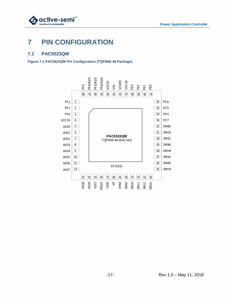
7 PIN CONFIGURATION
7.1 PAC5523QM
Figure 7-1 PAC5523QM Pin Configuration (TQFN66-48 Package)
DRH3
373839404142434445464748
11
PAC5523QMTQFN66-48 (6x6 mm)
10
9
8
7
6
5
4
3
2
PE0
PE1
PE2
PE3
VCC
18
VCO
RE
VSS
VCC
IO
PF6/
AD
6
PF5/
AD
5
PF4/
AD
4
PF3
PF2
PF1
PF0
VCC33
AIO0
AIO1
AIO2
AIO3
AIO4
AIO5
AIO
8
AIO
9
VSY
S
REG
O
CSM VP
DR
M
DR
L1
DR
L2
DR
S3
DRB3
DRS4
DRH4
DRB4
DRS5
DRH5
DRB5
PC7
PC4
PC5
EP (VSS)
242322212019181716151413
12
AIO6
AIO7
DR
L0
VH
M
26
27
28
29
30
31
32
33
34
35
25
PC6
Power Application Controller
-18- Rev 1.0 – May 11, 2018
8 PIN DESCRIPTION
Table 8-1 Multi-Mode Power Manager (MMPM) and System Pin Description
PIN NAME PIN
NUMBER TYPE DESCRIPTION
VCC33 4 Power Internally generated 3.3V power supply. Connect to a 2.2µF or higher value ceramic capacitor from VCC33 to VSSA.
VSYS 15 Power 5V System power supply. Connect to a 6.8F (20%) or higher ceramic capacitor from VSYS to VSS.
REGO 16 Power System regulator output. Connect to VSYS directly or through an external power-dissipating resistor.
CSM 17 Power Switching supply current sense input. Connect to the positive side of the current sense resistor.
VP 18 Power
Main power supply. Provides power to the power drivers as well as voltage feedback path for the switching supply. Connect a properly
sized supply bypass capacitor in parallel with a 0.1F ceramic capacitor from VP to VSS for voltage loop stabilization. This pin requires good capacitive bypassing to VSS, so the ceramic capacitor must be connected with a shorter than 10mm trace from the pin.
VHM 19 Power
Switching supply controller supply input. Connect a 1μF or higher value ceramic capacitor, or a 0.1μF ceramic capacitor in parallel with a 10μF or higher electrolytic capacitor from VHM to VSSP. This pin requires good capacitive bypassing to VSSP, so the ceramic capacitor must be connected with a shorter than 10mm trace from the pin.
DRM 20 Power Switching supply driver output. Connect to the base or gate of the external power NPN or n-channel MOSFET. See User Guide and application notes.
VCC18 41 Power Internally generated 1.8V power supply. Connect a 2.2F or higher value ceramic capacitor from VCC18 to VSSA.
VCORE 42 Power Internally generated 1.2V core power supply. Connect a 2.2F or higher value ceramic capacitor from VCORE to VSSA.
VSS 43 Power Ground.
VCCIO 44 Power Internally generated digital I/O 3.3V power supply. Connect a 4.7F or higher value ceramic capacitor from VCCIO to VSSA.
EP (VSS) EP Power Exposed pad. Must be connected to VSS in a star ground configuration. Connect to a large PCB copper area for power dissipation heat sinking.
Power Application Controller
-19- Rev 1.0 – May 11, 2018
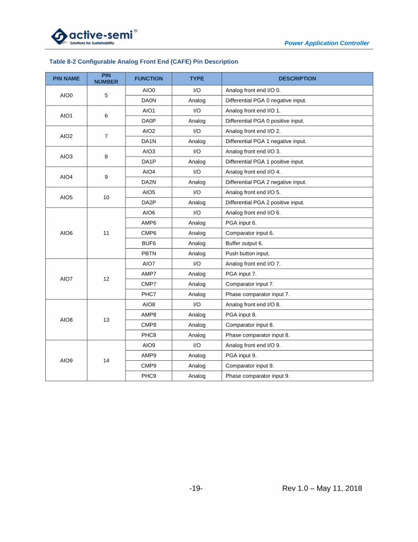
Table 8-2 Configurable Analog Front End (CAFE) Pin Description
PIN NAME PIN
NUMBER FUNCTION TYPE DESCRIPTION
AIO0 5 AIO0 I/O Analog front end I/O 0.
DA0N Analog Differential PGA 0 negative input.
AIO1 6 AIO1 I/O Analog front end I/O 1.
DA0P Analog Differential PGA 0 positive input.
AIO2 7 AIO2 I/O Analog front end I/O 2.
DA1N Analog Differential PGA 1 negative input.
AIO3 8 AIO3 I/O Analog front end I/O 3.
DA1P Analog Differential PGA 1 positive input.
AIO4 9 AIO4 I/O Analog front end I/O 4.
DA2N Analog Differential PGA 2 negative input.
AIO5 10 AIO5 I/O Analog front end I/O 5.
DA2P Analog Differential PGA 2 positive input.
AIO6 11
AIO6 I/O Analog front end I/O 6.
AMP6 Analog PGA input 6.
CMP6 Analog Comparator input 6.
BUF6 Analog Buffer output 6.
PBTN Analog Push button input.
AIO7 12
AIO7 I/O Analog front end I/O 7.
AMP7 Analog PGA input 7.
CMP7 Analog Comparator input 7.
PHC7 Analog Phase comparator input 7.
AIO8 13
AIO8 I/O Analog front end I/O 8.
AMP8 Analog PGA input 8.
CMP8 Analog Comparator input 8.
PHC8 Analog Phase comparator input 8.
AIO9 14
AIO9 I/O Analog front end I/O 9.
AMP9 Analog PGA input 9.
CMP9 Analog Comparator input 9.
PHC9 Analog Phase comparator input 9.
Power Application Controller
-20- Rev 1.0 – May 11, 2018
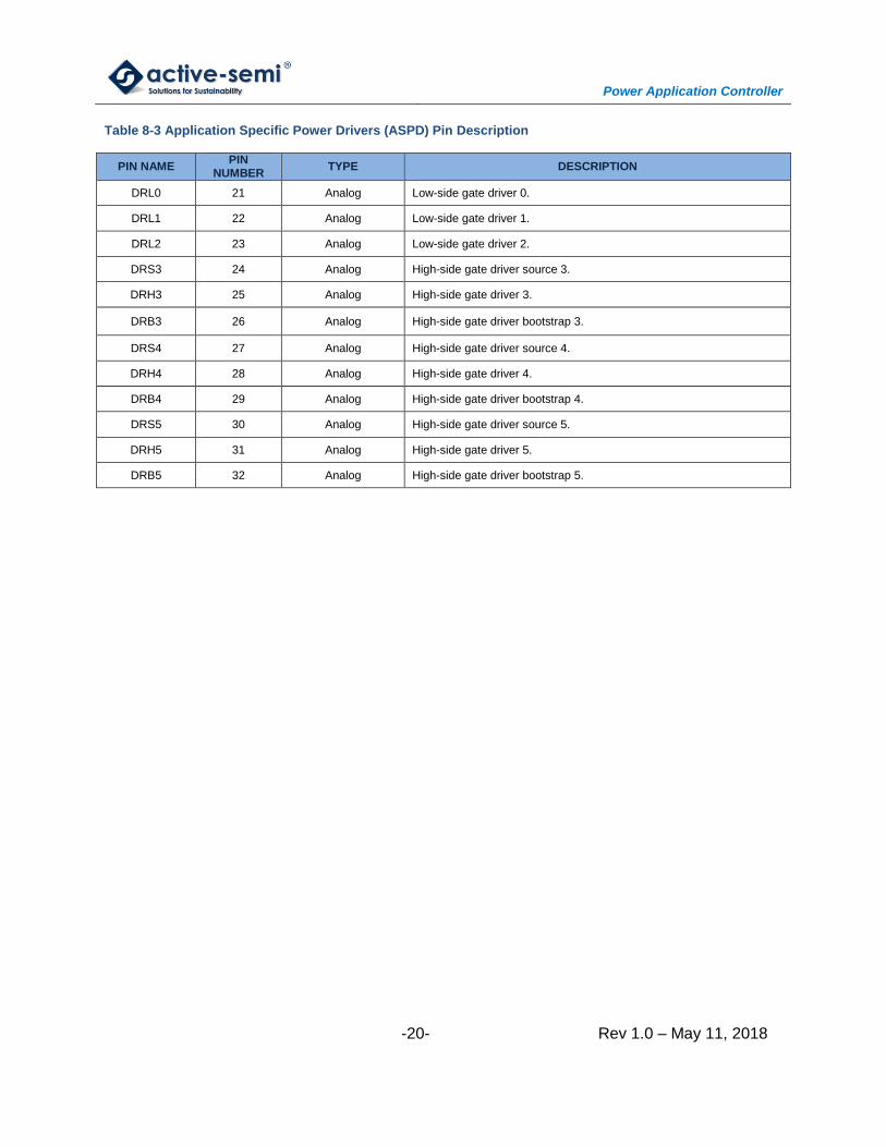
Table 8-3 Application Specific Power Drivers (ASPD) Pin Description
PIN NAME PIN
NUMBER TYPE DESCRIPTION
DRL0 21 Analog Low-side gate driver 0.
DRL1 22 Analog Low-side gate driver 1.
DRL2 23 Analog Low-side gate driver 2.
DRS3 24 Analog High-side gate driver source 3.
DRH3 25 Analog High-side gate driver 3.
DRB3 26 Analog High-side gate driver bootstrap 3.
DRS4 27 Analog High-side gate driver source 4.
DRH4 28 Analog High-side gate driver 4.
DRB4 29 Analog High-side gate driver bootstrap 4.
DRS5 30 Analog High-side gate driver source 5.
DRH5 31 Analog High-side gate driver 5.
DRB5 32 Analog High-side gate driver bootstrap 5.
Power Application Controller
-21- Rev 1.0 – May 11, 2018
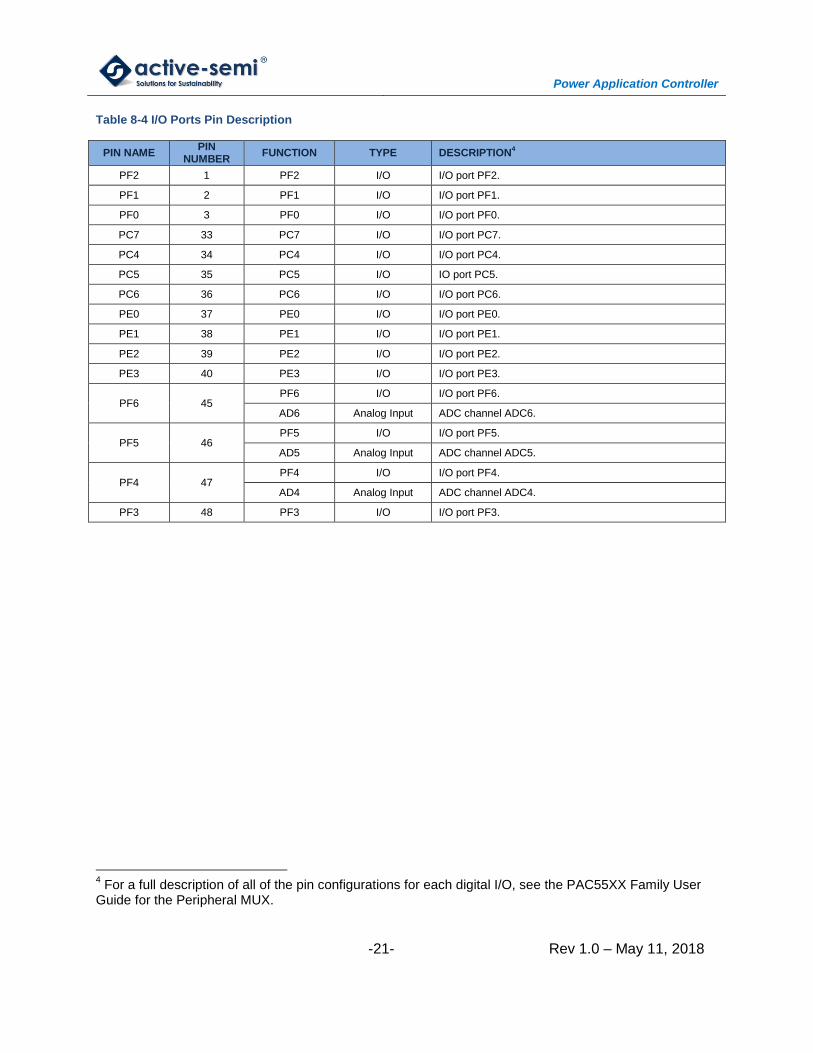
Table 8-4 I/O Ports Pin Description
PIN NAME PIN
NUMBER FUNCTION TYPE DESCRIPTION
4
PF2 1 PF2 I/O I/O port PF2.
PF1 2 PF1 I/O I/O port PF1.
PF0 3 PF0 I/O I/O port PF0.
PC7 33 PC7 I/O I/O port PC7.
PC4 34 PC4 I/O I/O port PC4.
PC5 35 PC5 I/O IO port PC5.
PC6 36 PC6 I/O I/O port PC6.
PE0 37 PE0 I/O I/O port PE0.
PE1 38 PE1 I/O I/O port PE1.
PE2 39 PE2 I/O I/O port PE2.
PE3 40 PE3 I/O I/O port PE3.
PF6 45 PF6 I/O I/O port PF6.
AD6 Analog Input ADC channel ADC6.
PF5 46 PF5 I/O I/O port PF5.
AD5 Analog Input ADC channel ADC5.
PF4 47 PF4 I/O I/O port PF4.
AD4 Analog Input ADC channel ADC4.
PF3 48 PF3 I/O I/O port PF3.
4 For a full description of all of the pin configurations for each digital I/O, see the PAC55XX Family User
Guide for the Peripheral MUX.
Power Application Controller
-22- Rev 1.0 – May 11, 2018
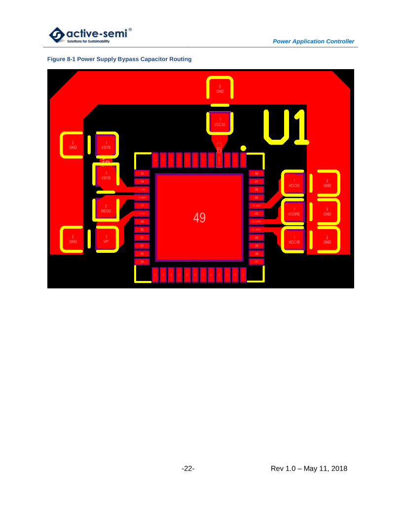
Figure 8-1 Power Supply Bypass Capacitor Routing
Power Application Controller
-23- Rev 1.0 – May 11, 2018
9 MULTI-MODE POWER MANAGER (MMPM)
9.1 Features
Multi-mode switching supply controller configurable as buck or SEPIC
DC supply up to 70V input
Direct DC input of up to 20V with no DC/DC
5 linear regulators with power and hibernate management, including VREF for ADC
Power and temperature monitor, warning, and fault detection
Figure 9-1 MMPM Block Diagram
MULTI-MODE POWER MANAGER
VPVOLTAGE
SETTING
POWER
OK & OVP
VSYS
LINEAR
REG
LINEAR
REG
LINEAR
REG
VCCIO VCC33 VCORE
TIMERS
HIBERNATE
2.5V VREF
VTHREF
POWER
& TEMP
MON
VMON
VTEMP
MULTI-MODE SWITCHING SUPPLY CONTROLLER
-
ERROR
AMP
+
-
COMP &
CURR LIMIT
ERROR
COMP
-
+
START UP &
MODE CTRL
PWM
LOGIC
CLAMP
DRIVER DRM
MU
X
CURR
SENSE
-
+ CSM
+
VHM1.2V
VSS
MU
X
IMOD
DAC
SYSTEM
SUPPLY
REGREGO
LINEAR
REG
VCC18
9.2 Functional Description
The Multi-Mode Power Manager (Figure 9-1) is optimized to efficiently provide “all-in-one” power
management required by the PAC and associated application circuitry. It incorporates a
dedicated multi-mode switching supply (MMSS) controller operable as a Buck or SEPIC
converter to efficiently convert power from a DC input source to generate a main supply output
VP. Five linear regulators provide VCC18, VSYS, VCCIO, VCC33, and VCORE supplies for MCU FLASH,
5V system, 3.3V I/O, 3.3V mixed signal, and 1.2V microcontroller core circuitry. The power
manager also handles system functions including internal reference generation, timers,
hibernate mode management, and power and temperature monitoring.
Power Application Controller
-24- Rev 1.0 – May 11, 2018
9.3 Multi-Mode Switching Supply (MMSS) Controller
The MMSS controller drives an external power transistor for pulse-width modulation switching of
an inductor or transformer for power conversion. The DRM output drives the gate of the N-CH
MOSFET or the base of the NPN between the VHM on state and VSSP off state at proper duty cycle
and switching frequency to ensure that the main supply voltage VP is regulated. The VP
regulation voltage is initially set to 15V during start up, and can be reconfigured to be 9V or 12V
by the microcontroller after initialization. When VP is lower than the target regulation voltage, the
internal feedback control circuitry causes the inductor current to increase to raise VP.
Conversely, when VP is higher than the regulation voltage, the feedback loop control causes the
inductor current to decrease to lower VP. The feedback loop is internally stabilized. The output
current capability of the switching supply is determined by the external current sense resistor. In
the high-side current sense buck or SEPIC mode, the inductor current signal is sensed
differentially between the CSM pin and VP, and has a peak current limit threshold of 0.26V.
The MMSS controller is flexible and configurable as a buck or SEPIC converter. Input sources
include battery supply for buck mode (Figure 9-2) or SEPIC mode (Figure 9-3). The MMSS
controller operational mode is determined by external configuration and register settings from
the microcontroller after power up. It can operate in either high-side or low-side current sense
mode, and does not require external feedback loop compensation circuitry.
Figure 9-2 Buck Mode
PAC5523
VP
DRM
CSM
VHM VIN
+++
+++
Power Application Controller
-25- Rev 1.0 – May 11, 2018
Figure 9-3 SEPIC Mode
PAC5523
VP
DRM
CSM
VHM VIN+++ ++
++
VP
The MMSS detects and selects between high-side and low-side mode during start up based on
the placement of the current sense resistor and the CSM pin voltage. It employs a safe start up
mode with a 9.5kHz switching frequency until VP exceeds 4.3V under-voltage-lockout threshold,
then transitions to the 45kHz default switching frequency for at least 6ms to bring VP close to the
target voltage, before enabling the linear regulators. Any extra load should only be applied after
the supplies are available and the microprocessor has initialized. The switching frequency can
be reconfigured by the microprocessor to be 181kHz to 500kHz in the high switching frequency
mode for battery-based applications, and to be 45kHz to 125kHz in the low switching frequency
mode. Upon initialization, the microcontroller must reconfigure the MMSS to the desired settings
for VP regulation voltage, switching mode, switching frequency, and VHM clamp. Refer to the PAC
application notes and user guide for MMSS controller design and programming.
If a stable external 5V to 20V power source is available, it can power the VP main supply and all
the linear regulators directly without requiring the MMSS controller to operate. In such
applications, VHM can be connected directly to VP and the microcontroller should disable the
MMSS upon initialization to reduce power loss.
Figure 9-4 Direct Battery Supply
PAC5523
VP
DRMCSM
++
VHM
VSS
VBAT
Power Application Controller
-26- Rev 1.0 – May 11, 2018
9.4 Linear Regulators
The MMPM includes four linear regulators. The system supply regulator (VSYS) is a medium
voltage regulator that takes the VP supply and sources up to 200mA at REGO until VSYS,
externally coupled to REGO, reaches 5V. This allows a properly rated external resistor to be
connected from REGO to VSYS to close the loop and offload power dissipation between VP and
VSYS.
Once VSYS is above 4V, the four additional linear regulators for VCC18, VCCIO, VCC33, and
VCORE supplies sequentially power up. Figure 9-5 shows typical circuit connections for the
linear regulators. The VCC18 regulator generates a dedicated 1.8V supply for FLASH on the
MCU. The VCCIO regulator generates a dedicated 3.3V supply for IO. The VCC33 and VCORE
regulators generate 3.3V and 1.2V, respectively. When VSYS, VCCIO, VCC33, and VCORE are
all above their respective power good thresholds, and the configurable power on reset duration
has expired, the microcontroller is initialized.
Figure 9-5 Linear Regulators
PAC5523
VCC33
VCCIO
VCORE
VSS
2.2F
2.2F
4.7F
REGO
VSYS4.7F
VSY S (5V)
2.2FVCC18
Power Application Controller
-27- Rev 1.0 – May 11, 2018
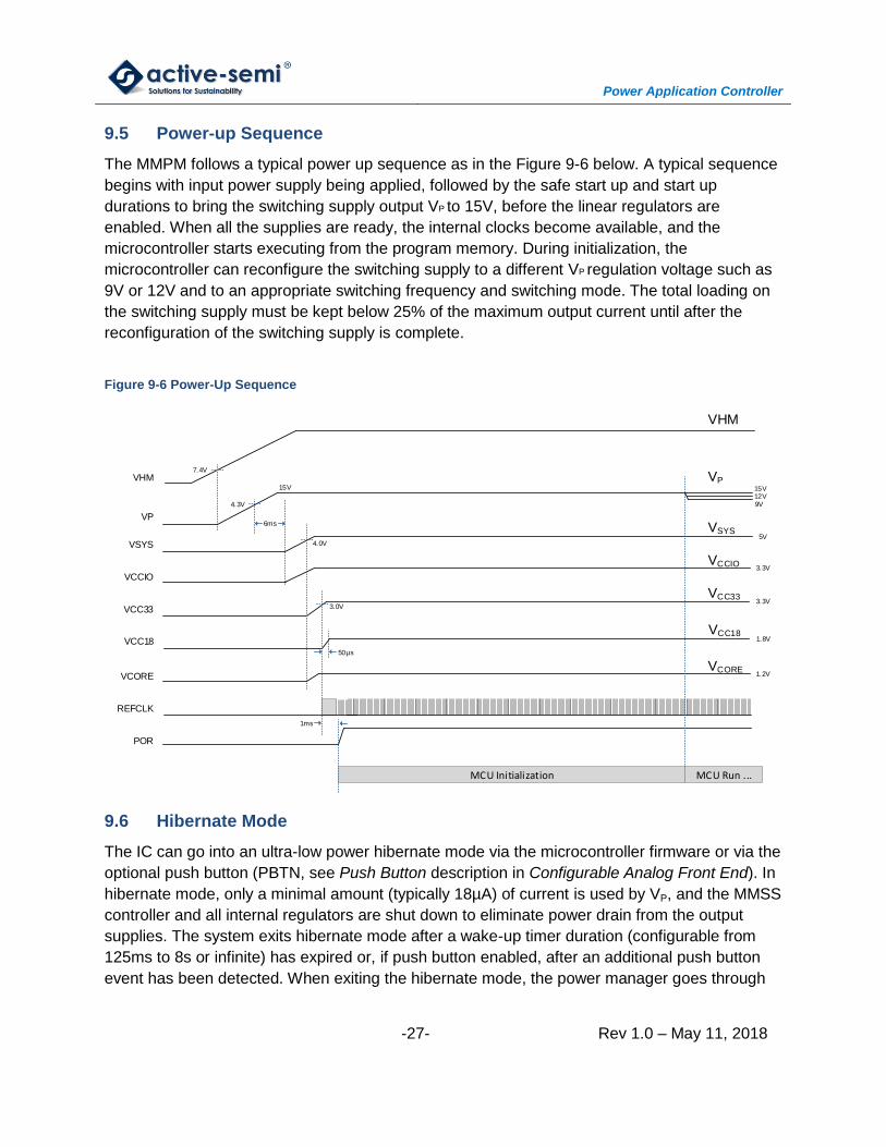
9.5 Power-up Sequence
The MMPM follows a typical power up sequence as in the Figure 9-6 below. A typical sequence
begins with input power supply being applied, followed by the safe start up and start up
durations to bring the switching supply output VP to 15V, before the linear regulators are
enabled. When all the supplies are ready, the internal clocks become available, and the
microcontroller starts executing from the program memory. During initialization, the
microcontroller can reconfigure the switching supply to a different VP regulation voltage such as
9V or 12V and to an appropriate switching frequency and switching mode. The total loading on
the switching supply must be kept below 25% of the maximum output current until after the
reconfiguration of the switching supply is complete.
Figure 9-6 Power-Up Sequence
VHM
VSYS
VCCIO
VCC33
VCORE
REFCLK
POR
7.4V
VP
4.3V
6ms
VHM
VP
VSYS
VCCIO
VCC33
VCORE
1ms
15V
9V
MCU Initialization MCU Run ...
5V
3.3V
3.3V
1.2V
12V
15V
VCC18VCC18
1.8V
3.0V
50µs
4.0V
9.6 Hibernate Mode
The IC can go into an ultra-low power hibernate mode via the microcontroller firmware or via the
optional push button (PBTN, see Push Button description in Configurable Analog Front End). In
hibernate mode, only a minimal amount (typically 18µA) of current is used by VP, and the MMSS
controller and all internal regulators are shut down to eliminate power drain from the output
supplies. The system exits hibernate mode after a wake-up timer duration (configurable from
125ms to 8s or infinite) has expired or, if push button enabled, after an additional push button
event has been detected. When exiting the hibernate mode, the power manager goes through
Power Application Controller
-28- Rev 1.0 – May 11, 2018
the start up cycle and the microcontroller is reinitialized. Only the persistent power manager
status bits (resets and faults) are retained during hibernation.
9.7 Power and Temperature Monitor
Whenever any of the VSYS, VCCIO, VCC33, or VCORE power supplies falls below their respective
power good threshold voltage, a fault event is detected and the microcontroller is reset. The
microcontroller stays in the reset state until VSYS, VCCIO, VCC33, and VCORE supply rails are all
good again and the reset time has expired. A microcontroller reset can also be initiated by a
maskable temperature fault event that occurs when the IC temperature reaches 170°C. The
fault status bits are persistent during reset, and can be read by the microcontroller upon re-
initialization to determine the cause of previous reset.
A power monitoring signal VMON is provided onto the ADC pre-multiplexer for monitoring various
internal power supplies. VMON can be set to be VCORE, 0.4•VCC33, 0.4•VCCIO, 0.4•VSYS,
0.1•VREGO, 0.1•VP, or the internal compensation voltage VCOMP for switching supply power
monitoring.
For power and temperature warning, an IC temperature warning event at 140°C are provided as
a maskable interrupt to the microcontroller. This warning allows the microcontroller to safely
power down the system.
In addition to the temperature warning interrupt and fault reset, a temperature monitor signal
VTEMP = 1.5 + 5.04e-3 • (T - 25°C) (V) is provided onto the ADC pre-multiplexer for IC
temperature measurement.
9.8 Voltage Reference
The reference block includes a 2.5V high precision reference voltage that provides the 2.5V
reference voltage for the ADC, the DACs, and the 4-level programmable threshold voltage
VTHREF (0.1V, 0.2V, 0.5V, and 1.25V).
Power Application Controller
-29- Rev 1.0 – May 11, 2018
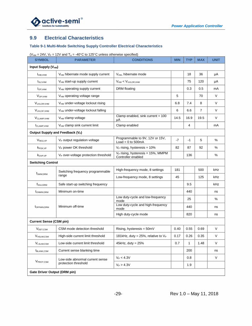
9.9 Electrical Characteristics
Table 9-1 Multi-Mode Switching Supply Controller Electrical Characteristics
(VHM = 24V, VP = 12V and TA = -40C to 125C unless otherwise specified)
SYMBOL PARAMETER CONDITIONS MIN TYP MAX UNIT
Input Supply (VHM)
IHIB;VHM VHM hibernate mode supply current VHM, hibernate mode 18 36 µA
ISU;VHM VHM start-up supply current VHM < VUVLOR;VHM 75 120 µA
IOP;VHM VHM operating supply current DRM floating 0.3 0.5 mA
VOP;VHM VHM operating voltage range 5 70 V
VUVLOR;VHM VHM under-voltage lockout rising 6.8 7.4 8 V
VUVLOF;VHM VHM under-voltage lockout falling 6 6.6 7 V
VCLAMP;VHM VHM clamp voltage Clamp enabled, sink current = 100 µA
14.5 16.9 19.5 V
ICLAMP;VHM VHM clamp sink current limit Clamp enabled 4 mA
Output Supply and Feedback (VP)
VREG;VP VP output regulation voltage Programmable to 9V, 12V or 15V, Load = 0 to 500mA
-7 -1 5 %
kPOK;VP VP power OK threshold VP rising, hysteresis = 10% 82 87 92 %
kOVP;VP VP over-voltage protection threshold VP rising, hysteresis = 15%, MMPM Controller enabled
136 %
Switching Control
fSWM;DRM Switching frequency programmable range
High-frequency mode, 8 settings 181 500 kHz
Low-frequency mode, 8 settings 45 125 kHz
fSSU;DRM Safe start-up switching frequency 9.5 kHz
tONMIN;DRM Minimum on-time 440 ns
tOFFMIN;DRM Minimum off-time
Low duty-cycle and low-frequency mode
25 %
Low duty-cycle and high-frequency mode
440 ns
High duty-cycle mode 820 ns
Current Sense (CSM pin)
VDET;CSM CSM mode detection threshold Rising, hysteresis = 50mV 0.40 0.55 0.69 V
VHSLIM;CSM High-side current limit threshold 181kHz, duty = 25%, relative to VP 0.17 0.26 0.35 V
VLSLIM;CSM Low-side current limit threshold 45kHz, duty = 25% 0.7 1 1.48 V
tBLANK;CSM Current sense blanking time 200 ns
VPROT;CSM Low-side abnormal current sense protection threshold
VP < 4.3V 0.8 V
VP > 4.3V 1.9
Gate Driver Output (DRM pin)
Power Application Controller
-30- Rev 1.0 – May 11, 2018
VOH;DRM High-level output voltage 5% IOH, relative to VHM VHM –
1 V
VOL;DRM Low-level output voltage 5% IOL 0.6 V
IOH;DRM High-level output source current VDRM = VHM – 5V -0.3 A
IOL;DRM Low-level output sink current VDRM = 5V 0.5 A
tPD;DRM Strong pull-down pulse width High-side current sense mode 240 ns
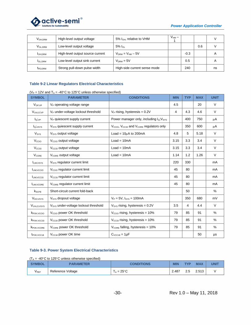
Table 9-2 Linear Regulators Electrical Characteristics
(VP = 12V and TA = -40C to 125C unless otherwise specified)
SYMBOL PARAMETER CONDITIONS MIN TYP MAX UNIT
VOP;VP VP operating voltage range 4.5 20 V
VUVLO;VP VP under-voltage lockout threshold VP rising, hysteresis = 0.2V 4 4.3 4.6 V
IQ;VP VP quiescent supply current Power manager only, including IQ;VSYS 400 750 A
IQ;VSYS VSYS quiescent supply current VCCIO, VCC33 and VCORE regulators only 350 600 A
VSYS VSYS output voltage Load = 10A to 200mA 4.8 5 5.18 V
VCCIO VCCIO output voltage Load = 10mA 3.15 3.3 3.4 V
VCC33 VCC33 output voltage Load = 10mA 3.15 3.3 3.4 V
VCORE VCORE output voltage Load = 10mA 1.14 1.2 1.26 V
ILIM;VSYS VSYS regulator current limit 220 330 mA
ILIM;VCCIO VCCIO regulator current limit 45 80 mA
ILIM;VCC33 VCC33 regulator current limit 45 80 mA
ILIM;VCORE VCORE regulator current limit 45 80 mA
kSCFB Short-circuit current fold-back 50 %
VDO;VSYS VSYS dropout voltage VP = 5V, ISYS = 100mA 350 680 mV
VUVLO;VSYS VSYS under-voltage lockout threshold VSYS rising, hysteresis = 0.2V 3.5 4 4.4 V
kPOK;VCCIO VCCIO power OK threshold VCCIO rising, hysteresis = 10% 79 85 91 %
kPOK;VCC33 VCC33 power OK threshold VCC33 rising, hysteresis = 10% 79 85 91 %
kPOK;VCORE VCORE power OK threshold VCORE falling, hysteresis = 10% 79 85 91 %
tPOK;VCC18 VCC18 power OK time CVCC18 = 1µF 50 µs
Table 9-3. Power System Electrical Characteristics
(TA = -40C to 125C unless otherwise specified)
SYMBOL PARAMETER CONDITIONS MIN TYP MAX UNIT
VREF Reference Voltage TA = 25C 2.487 2.5 2.513 V
Power Application Controller
-31- Rev 1.0 – May 11, 2018
TA = -40C to 125C 2.463 2.5 2.537 V
kMON Power monitoring voltage (VMON) coefficient
VCORE 1
V/V VSYS, VCCIO, VCC33 0.4
VP, VREGO 0.1
VTEMP Temperature monitor voltage at 25C TA = 25C, at ADC 1.475 1.5 1.54 V
kTEMP Temperature monitor coefficient At ADC 5.04 mV/K
TWARN Over-temperature warning threshold Hysteresis = 10C 140 C
TFAULT Over-temperature fault threshold Hysteresis = 10C 170 C
Power Application Controller
-32- Rev 1.0 – May 11, 2018
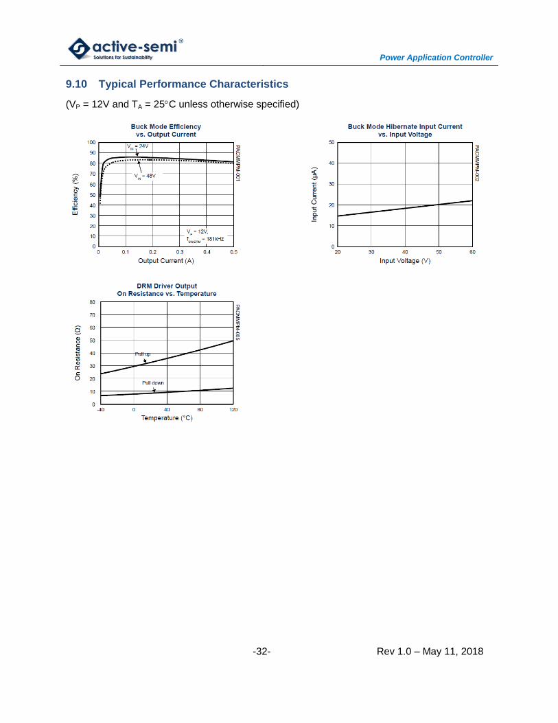
9.10 Typical Performance Characteristics
(VP = 12V and TA = 25C unless otherwise specified)
Power Application Controller
-33- Rev 1.0 – May 11, 2018
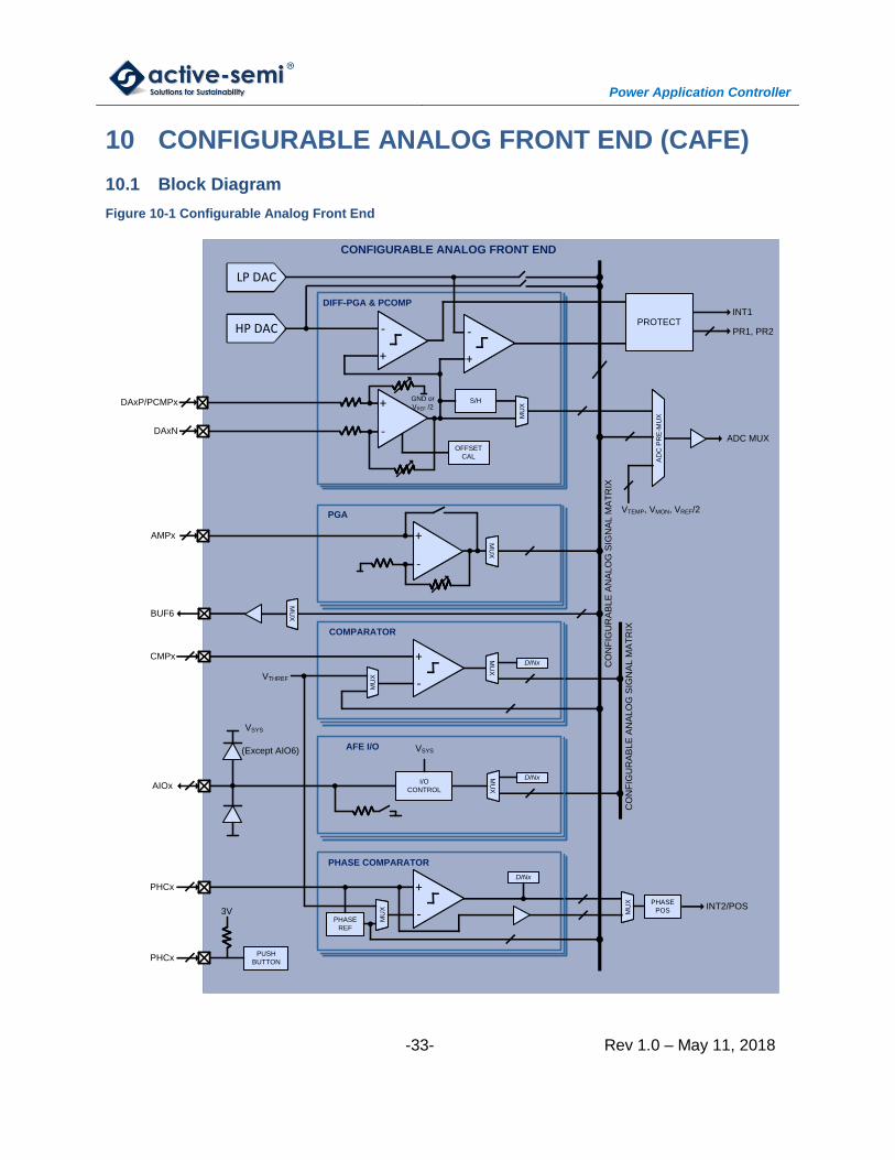
10 CONFIGURABLE ANALOG FRONT END (CAFE)
10.1 Block Diagram
Figure 10-1 Configurable Analog Front End
CONFIGURABLE ANALOG FRONT END
+
-
+
-
+
-
+
-
+ S/HDAxP/PCMPx
LP DACLP DAC
HP DACHP DAC
DIFF-PGA & PCOMP
+
-
+
-
+
MU
XM
UX
OFFSET
CAL
PROTECTINT1
PR1, PR2
AD
C P
RE
-MU
XA
DC
PR
E-M
UX
DAxNADC MUX
VTEMP, VMON, VREF/2
CO
NF
IGU
RA
BL
E A
NA
LO
G S
IGN
AL
MA
TR
IX
-
+
-
+AMPx
PGA
MU
XM
UX
MU
XM
UXBUF6
COMPARATOR
MU
XM
UX
DINx
CO
NF
IGU
RA
BL
E A
NA
LO
G S
IGN
AL
MA
TR
IX
+
-
+
-MU
XM
UX
CMPx
VTHREF
AFE I/O
DINxMU
XM
UX
I/O
CONTROLAIOx
VSYS
VSYS
(Except AIO6)
PHASE COMPARATOR
DINx
+
-
+
-
MU
XM
UX
PHCx
PHASE
REF
PUSH
BUTTONPHCx
3V MU
XM
UX PHASE
POSINT2/POS
GND or
VREF /2
Power Application Controller
-34- Rev 1.0 – May 11, 2018
10.2 Functional Description
The device includes a Configurable Analog Front End (CAFE, Figure 10-1) accessible through
10 analog and I/O pins. These pins can be configured to form flexible interconnected circuitry
made up of 3 differential programmable gain amplifiers, 4 single-ended programmable gain
amplifiers, 4 general purpose comparators, 3 phase comparators, 10 protection comparators,
and one buffer output. These pins can also be programmed as analog feed-through pins, or as
analog front end I/O pins that can function as digital inputs or digital open-drain outputs. The
PAC proprietary configurable analog signal matrix (CASM) and configurable digital signal matrix
(CDSM) allow real time asynchronous analog and digital signals to be routed in flexible circuit
connections for different applications. A push button function is provided for optional push
button on, hibernate, and off power management function.
10.3 Differential Programmable Gain Amplifier (DA)
The DAxP and DAxN pin pair are positive and negative inputs, respectively, to a differential
programmable gain amplifier. The differential gain can be programmable to be 1x, 2x, 4x, 8x,
16x, 32x, and 48x for zero ohm signal source impedance. The differential programmable gain
amplifier has -0.3V to 3.5V input common mode range, and its output can be configured for
routing directly to the ADC pre-multiplexer, or through a sample-and-hold circuit synchronized
with the ADC auto-sampling mechanism. Each differential amplifier is accompanied by offset
calibration circuitry, and two protection comparators for protection event monitoring. The
programmable gain differential amplifier is optimized for use with signal source impedance lower
than 500Ω and with matched source impedance on both positive and negative inputs for
minimal offset. The effective gain is scaled by 13.5k / (13.5k + RSOURCE), where RSOURCE is the
matched source impedance of each input.
10.4 Single-Ended Programmable Gain Amplifier (AMP)
Each AMPx input goes to a single-ended programmable gain amplifier with signal relative to
VSSA. The amplifier gain can be programmed to be 1x, 2x, 4x, 8x, 16x, 32x, and 48x, or as
analog feed-through. The programmable gain amplifier output is routed via a multiplexer to the
configurable analog signal matrix CASM.
10.5 General Purpose Comparator (CMP)
The general purpose comparator takes the CMPx input and compares it to either the
programmable threshold voltage (VTHREF) or a signal from the configurable analog signal matrix
CASM. The comparator has 0V to VSYS input common mode range, and its polarity-selectable
output is routed via a multiplexer to either a data input bit or the configurable digital signal matrix
CDSM. Each general purpose comparator has two mask bits to prevent or allow rising or falling
edge of its output to trigger second microcontroller interrupt INT2, where INT2 can be
configured to active protection event PR1.
Power Application Controller
-35- Rev 1.0 – May 11, 2018
10.6 Phase Comparator (PHC)
The phase comparator takes the PHCx input and compares it to either the programmable
threshold voltage (VTHREF) or a signal from the configurable analog signal matrix CASM. The
comparison signal can be set to a phase reference signal generated by averaging the PHCx
input voltages. In a three-phase motor control application, the phase reference signal acts as a
virtual center tap for BEMF detection. The PHCx inputs are optionally fed through to the CASM.
The PHC inputs can be compared to the virtual center-tap, or phase to phase for the most
efficient BEMF zero-cross detection. The phase comparators have configurable asymmetric
hysteresis.
The phase comparator has 0V to VSYS input common mode range, and its polarity-selectable
output is routed to a data input bit and to the phase/position multiplexer synchronized with the
auto-sampling sequencers.
10.7 Protection Comparator (PCMP)
Two protection comparators are provided in association with each differential programmable
gain amplifier, with outputs available to trigger protection events and accessible as read-back
output bits. The high-speed protection (HP) comparator compares the PCMPx pin to the 8-bit
HP DAC output voltage, with full scale voltage of 2.5V. The limit protection (LP) comparator
compares the differential programmable gain amplifier output to the 10-bit LP DAC output
voltage, with full scale voltage of 2.5V.
Each protection comparator has a mask bit to prevent or allow it to trigger the main
microcontroller interrupt INT1. Each protection comparator also has one mask bit to prevent or
allow it to activate protection event PR1, and another mask bit to prevent or allow it to activate
protection event PR2. These two protection events can be used directly by protection circuitry in
the Application Specific Power Drivers (ASPD) to protect devices being driven.
10.8 Analog Output Buffer (BUF)
A subset of the signals from the configurable analog signal matrix CASM can be multiplexed to
the BUF6 pin for external use. The buffer offset voltage can be minimized with the built-in swap
function.
10.9 Analog Front End I/O (AIO)
Up to 10 AIOx pins are available in the device, depending on the product5. In the analog front
end I/O mode, the pin can be configured to be a digital input or digital open-drain output. The
AIOx input or output signal can be set to a data input or output register bit, or multiplexed to one
of the signals in the configurable digital signal matrix CDSM. The signal can be set to active
5 See the pin configuration and description for specific information on which pins are available in this
product.
Power Application Controller
-36- Rev 1.0 – May 11, 2018
high (default) or active low, with VSYS supply rail. Where AIO6,7,8,9 supports microcontroller
interrupt for external signals. Each has two mask bits to prevent or allow rising or falling edge of
its corresponding digital input to trigger second microcontroller interrupt INT2.
10.10 Push Button (PBTN)
The push button PBTN, when enabled, can be used by the MCU to detect a user active-low
push button event and to put the system into an ultra-low-power hibernate mode. Once the
system is in hibernate mode, PBTN can be used to wake up the system.
In addition, PBTN can also be used as a hardware reset for the microcontroller when it is held
low for longer than 8s during normal operation. The PBTN input is active low and has a 55kΩ
pull-up resistor to 3V.
10.11 HP DAC and LP DAC
The 8-bit HP DAC can be used as the comparison voltage for the high-speed protection (HP)
comparators, or routed for general purpose use via the AB2 signal in the CASM. The HP DAC
output full scale voltage is 2.5V.
The 10-bit LP DAC can be used as the comparison voltage for the limit protection (LP)
comparators, or routed for general purpose use via the AB3 signal in the CASM. The LP DAC
output full scale voltage is 2.5V.
10.12 ADC Pre-Multiplexer
The ADC pre-multiplexer is a 16-to-1 multiplexer that selects between the 3 differential
programmable gain amplifier outputs, AB1 through AB9, temperature monitor signal (VTEMP),
power monitor signal (VMON), and offset calibration reference (VREF / 2). The ADC pre-multiplexer
can be directly controlled or automatically scanned by the auto-sampling sequencer.
When the ADC pre-multiplexer is automatically scanned, the unbuffered or sensitive signals
should be masked by setting appropriate register bits.
10.13 Configurable Analog Signal Matrix (CASM)
The CASM has 12 general purpose analog signals labeled AB1 through AB12 that can be used
for:
Routing the single-ended programmable gain amplifier or analog feed-through output to
AB1 through AB9
Routing an analog signal via AB1, AB2, or AB3 to the negative input of a general
purpose comparator or phase comparator
Routing the 8-bit HP DAC output to AB2
Routing the 10-bit LP DAC output to AB3
Power Application Controller
-37- Rev 1.0 – May 11, 2018
Routing analog signals via AB1 through AB12 to the ADC pre-multiplexer
Routing phase comparator feed-through signals to AB7, AB8, and AB9, and averaged
voltage to AB1
10.14 Configurable Digital Signal Matrix (CDSM)
The CDSM has 7 general purpose bi-directional digital signals labeled DB1 through DB7 that
can be used for:
Routing the AIOx input to or output signals from DB1 through DB7
Routing the general purpose comparator output signals to DB1 through DB7
Power Application Controller
-38- Rev 1.0 – May 11, 2018
10.15 Electrical Characteristics
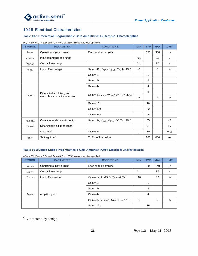
Table 10-1 Differential Programmable Gain Amplifier (DA) Electrical Characteristics
(VSYS = 5V, VCCIO = 3.3V and TA = -40C to 125C unless otherwise specified.)
SYMBOL PARAMETER CONDITIONS MIN TYP MAX UNIT
ICC;DA Operating supply current Each enabled amplifier 150 300 A
VICMR;DA Input common mode range -0.3 3.5 V
VOLR;DA Output linear range 0.1 3.5 V
VOS;DA Input offset voltage Gain = 48x, VDAxP=VDAxN=0V, TA=25C -8 8 mV
AVZI;DA Differential amplifier gain (zero ohm source impedance)
Gain = 1x 1
Gain = 2x 2
Gain = 4x 4
Gain = 8x, VDAxP=VDAxN=0V, TA = 25C 8
-2 2 %
Gain = 16x 16
Gain = 32x 32
Gain = 48x 48
kCMRR;DA Common mode rejection ratio Gain = 8x, VDAxP=VDAxN=0V, TA = 25C 55 dB
RINDIF;DA Differential input impedance 27 kΩ
Slew rate6 Gain = 8x 7 10 V/s
tST;DA Settling time6 To 1% of final value 200 400 ns
Table 10-2 Single-Ended Programmable Gain Amplifier (AMP) Electrical Characteristics
(VSYS = 5V, VCCIO = 3.3V and TA = -40C to 125C unless otherwise specified.)
SYMBOL PARAMETER CONDITIONS MIN TYP MAX UNIT
ICC;AMP Operating supply current Each enabled amplifier 80 140 A
VOLR;AMP Output linear range 0.1 3.5 V
VOS;AMP Input offset voltage Gain = 1x, TA=25C, VAMPX=2.5V -10 10 mV
AV;AMP Amplifier gain
Gain = 1x 1
Gain = 2x 2
Gain = 4x 4
Gain = 8x, VAMPx=125mV, TA = 25C -2 2 %
Gain = 16x 16
6 Guaranteed by design
Power Application Controller
-39- Rev 1.0 – May 11, 2018
Gain = 32x 32
Gain = 48x 48
IIN;AMP Input current 0 1 A
Slew rate6 Gain = 8x 8 12 V/s
tST;AMP Settling time6 To 1% of final value 150 300 ns
Table 10-3 General Purpose Comparator (CMP) Electrical Characteristics
(VSYS = 5V, VCC33 = 3.3V and TA = -40C to 125C unless otherwise specified.)
SYMBOL PARAMETER CONDITIONS MIN TYP MAX UNIT
ICC;CMP Operating supply current Each enabled amplifier 35 110 A
VICMR;CMP Input common mode range 0 VSYS V
VOS;CMP Input offset voltage VCMPx=2.5V, TA=25C -10 10 mV
VHYS;CMP Hysteresis 20 mV
IIN;CMP Input current 0 1 A
tDEL;CMP Comparator delay6
100 ns
Table 10-4 Phase Comparator (PHC) Electrical Characteristics
(VSYS = 5V, VCC33 = 3.3V and TA = -40C to 125C unless otherwise specified.)
SYMBOL PARAMETER CONDITIONS MIN TYP MAX UNIT
ICC;PHC Operating supply current Each enabled amplifier 35 110 A
VICMR;PHC Input common mode range 0 VSYS V
VOS;PHC Input offset voltage VPCMPx=2.5V, TA=25C -10 10 mV
VHYS;PHC Hysteresis 20 mV
IIN;PHC Input current 0 1 A
tDEL;PHC Comparator delay6 100 ns
Table 10-5 Protection Comparator (PCMP) Electrical Characteristics
(VSYS = 5V, VCC33 = 3.3V and TA = -40C to 125C unless otherwise specified.)
SYMBOL PARAMETER CONDITIONS MIN TYP MAX UNIT
ICC;PCMP Operating supply current Each enabled comparator 35 100 A
VICMR;PCMP Input common mode range 0.3 VSYS-1 V
VOS;PCMP Input offset voltage VCMPx=2.5V, TA=25C -10 10 mV
VHYS;PCMP Hysteresis 20 mV
IIN;PCMP Input current 0 1 A
Power Application Controller
-40- Rev 1.0 – May 11, 2018
tDEL;PCMP Comparator delay6 100 ns
Table 10-6 Analog Output Buffer (BUF) Electrical Characteristics
(VSYS = 5V, VCCIO = 3.3V, and TA = -40C to 125C unless otherwise specified.)
SYMBOL PARAMETER CONDITIONS MIN TYP MAX UNIT
ICC;BUF Operating supply current No load 35 100 A
VICMR;BUF Input common mode range 0 3.5 V
VOLR;AMP Output linear range 0.1 3.5 V
VOS;BUF Offset voltage VBUF = 2.5V, TA = 25C -18 18 mV
IOMAX Maximum output current CL = 0.1nF 0.8 1.3 mA
Table 10-7 Analog Front End (AIO) Electrical Characteristics
(VSYS = 5V, VCCIO = 3.3V, and TA = -40C to 125C unless otherwise specified.)
SYMBOL PARAMETER CONDITIONS MIN TYP MAX UNIT
VAIO Pin voltage range 0 5 V
VIH;AIO High-level input voltage 2.2 V
VIL;AIO Low-level input voltage 0.8 V
RPD;AIO Pull-down resistance Input mode 0.5 1 1.8 MΩ
VOL;AIO Low-level output voltage
IAIO<9:7,3:1>=7mA, open-drain output mode
0.4
V IAIO<6,0>=7mA, open-drain output mode
0.5
IOL;AIO Low-level output sink current VAIOx = 0.4V, open-drain output mode
6 14 mA
ILK;AIO High-level output leakage current VAIOx = 5V, open-drain output mode 0 10 A
Table 10-8 Push Button (PBTN) Electrical Characteristics
(VSYS = 5V, VCCIO = 3.3V, and TA = -40C to 125C unless otherwise specified.)
SYMBOL PARAMETER CONDITIONS MIN TYP MAX UNIT
VI;PBTN Input voltage range 0 5 V
VIH;PBTN High-level input voltage 2 V
VIL;PBTN Low-level input voltage 0.35 V
RPU;PBTN Pull-up resistance To 3V, push-button input mode 40 55 95 kΩ
Power Application Controller
-41- Rev 1.0 – May 11, 2018
Table 10-9 HP DAC and LP DAC Electrical Characteristics
(VSYS = 5V, VCCIO = 3.3V, and TA = -40C to 125C unless otherwise specified.)
SYMBOL PARAMETER CONDITIONS MIN TYP MAX UNIT
VDACREF DAC reference voltage TA = 25C 2.48 2.5 2.52
V TA = -40C to 125C 2.453 2.5 2.547
HP 8-bit DAC INL7 -1 1 LSB
HP 8-bit DAC DNL7 -0.5 0.5 LSB
LP 10-bit DAC INL7 -2 2 LSB
LP 10-bit DAC DNL7 -1 1 LSB
7 Guaranteed by design and characterization
Power Application Controller
-42- Rev 1.0 – May 11, 2018
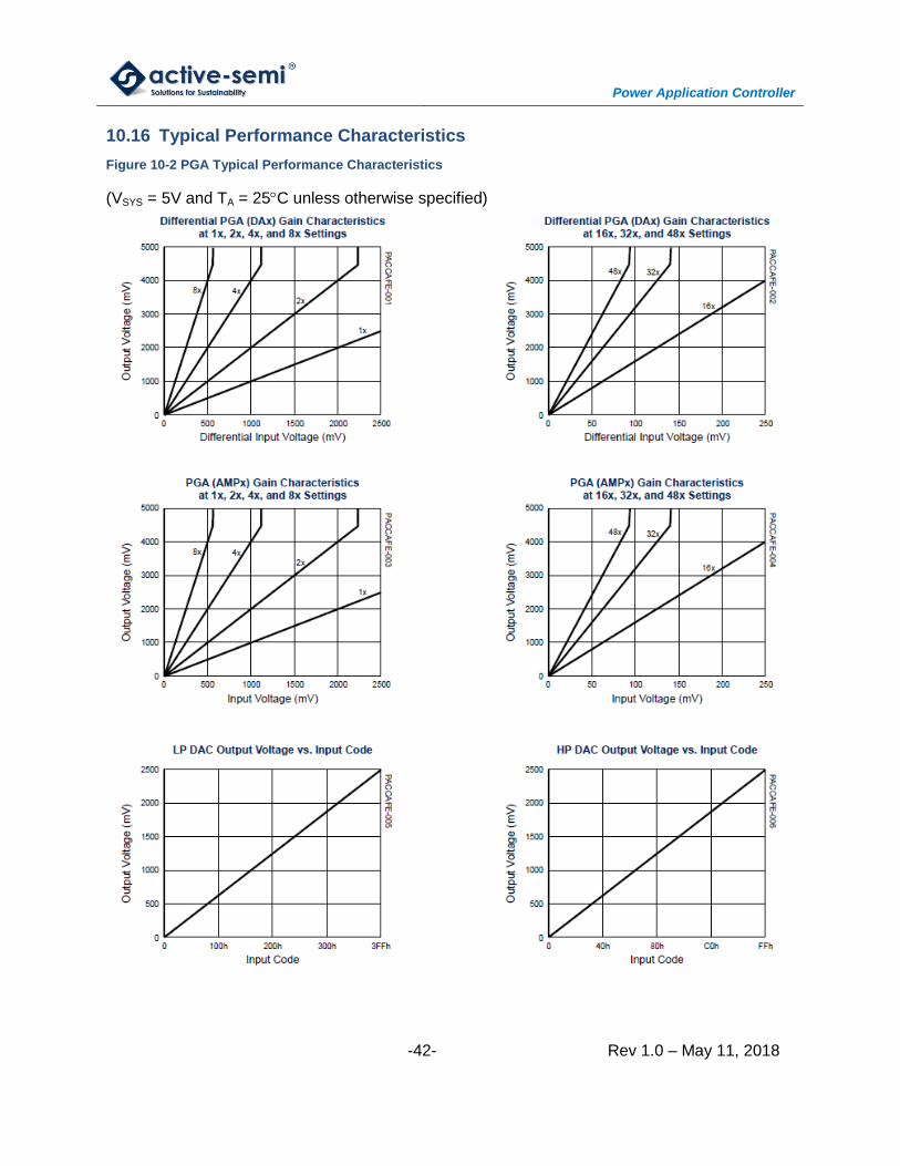
10.16 Typical Performance Characteristics
Figure 10-2 PGA Typical Performance Characteristics
(VSYS = 5V and TA = 25C unless otherwise specified)
Power Application Controller
-43- Rev 1.0 – May 11, 2018
11 APPLICATION SPECIFIC POWER DRIVERS
(ASPD)
11.1 Features
3 low-side and 3 high-side gate drivers
1.5A gate driving capability
Configurable delays and fast fault protection
11.2 Block Diagram
Figure 11-1 Application Specific Power Drivers
APPLICATION SPECIFIC POWER DRIVERS
HIGH-SIDE GATE DRIVERS
PRE-
DRIVER DRHx
DRSx
DRBx
DELAYLEVEL
SHIFTBBM
FAULT
PROTECT
HS
PO
RT
/PW
M S
IGN
AL
S
LOW-SIDE GATE DRIVERS
PRE-
DRIVER DRLxDELAY BBM
LS
ENDRV
VP
11.3 Functional Description
The Application Specific Power Drivers (ASPD, Figure 11-1) module handles power driving for
power and motor control applications. The ASPD contains three low-side gate drivers (DRLx),
three high-side gate drivers (DRHx). Each gate driver can drive an external MOSFET or IGBT
switch in response to high-speed control signals from the microcontroller ports, and a pair of
high-side and low-side gate drivers can form a half-bridge driver.
Figure 11-2 below shows typical gate driver connections and Table 11-1 shows the ASPD
available resources. The ASPD gate drivers support up to a 70V supply.
Power Application Controller
-44- Rev 1.0 – May 11, 2018
Figure 11-2 Typical Gate Driver Connections
MM
PAC5523DRBx
DRHxDRSx
DRLx
VP
VMO TO R
Table 11-1 Power Driver Resources by Part Numbers
PART NUMBER
LOW-SIDE GATE DRIVER HIGH-SIDE GATE DRIVER
DRLx SOURCE/SINK CURRENT DRHx MAX SUPPLY SOURCE/SINK CURRENT
PAC5523 3 1.5A/1.5A 3 70V 1.5A/1.5A
The ASPD includes built-in configurable fault protection for the internal gate drivers.
11.4 Low-Side Gate Driver
The DRLx low-side gate driver drives the gate of an external MOSFET or IGBT switch between
the low-level VSSP power ground rail and high-level VP supply rail. The DRLx output pin has
sink and source output current capability of 1.5A. Each low-side gate driver is controlled by a
microcontroller port signal with 4 configurable levels of propagation delay.
11.5 High-Side Gate Driver
The DRHx high-side gate driver drives the gate of an external MOSFET or IGBT switch between
its low-level DRSx driver source rail and its high-level DRBx bootstrap rail. The DRSx pin can go
up to 70V steady state. The DRHx output pin has sink and source output current capability of
1.5A. The DRBx bootstrap pin can have a maximum operating voltage of 16V relative to the
DRSx pin, and up to 82V steady state. The DRSx pin is designed to tolerate momentary
switching negative spikes down to -5V without affecting the DRHx output state. Each high-side
gate driver is controlled by a microcontroller port signal with 4 configurable levels of propagation
delay.
For bootstrapped high-side operation, connect an appropriate capacitor between DRBx and
DRSx and a properly rated bootstrap diode from VP to DRBx. To operate the DRHx output as a
low-side gate driver, connect its DRBx pin to VP and its DRSx pin to VSSP.
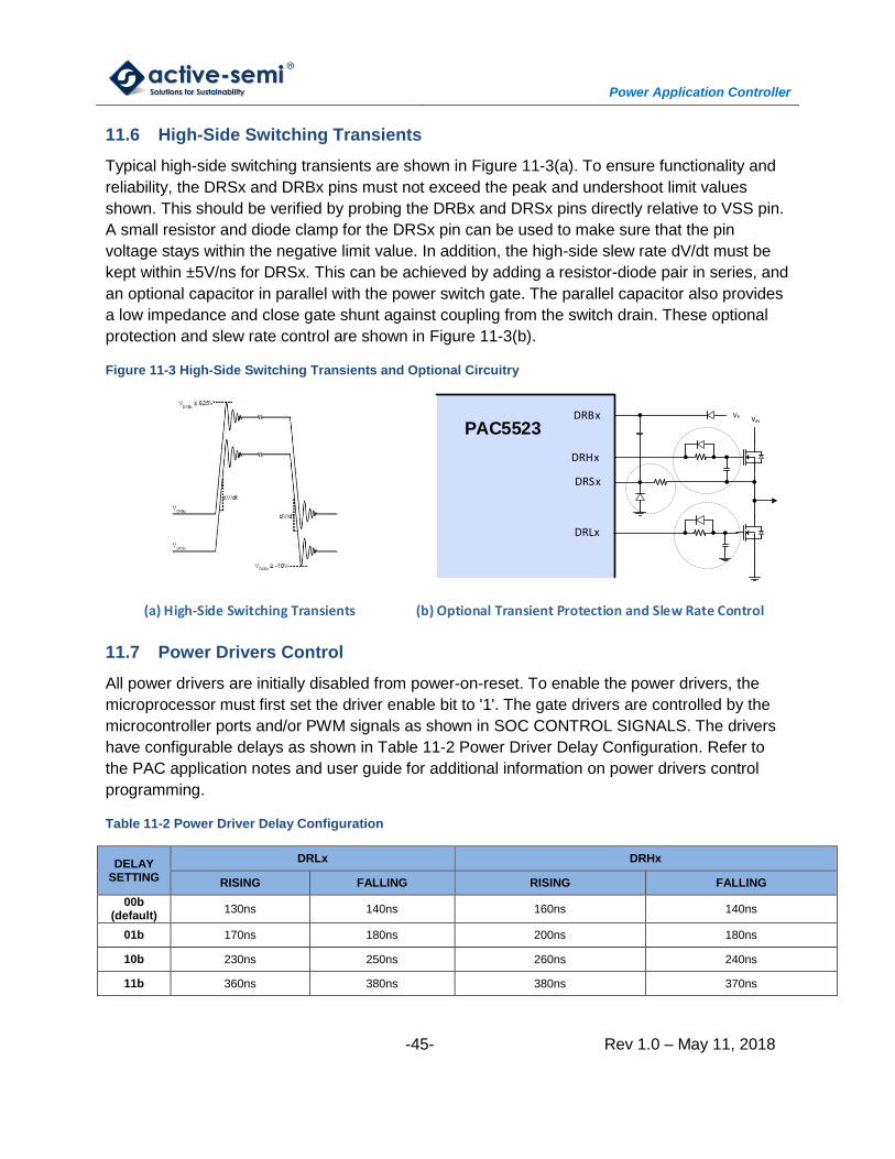
Power Application Controller
-45- Rev 1.0 – May 11, 2018
11.6 High-Side Switching Transients
Typical high-side switching transients are shown in Figure 11-3(a). To ensure functionality and
reliability, the DRSx and DRBx pins must not exceed the peak and undershoot limit values
shown. This should be verified by probing the DRBx and DRSx pins directly relative to VSS pin.
A small resistor and diode clamp for the DRSx pin can be used to make sure that the pin
voltage stays within the negative limit value. In addition, the high-side slew rate dV/dt must be
kept within ±5V/ns for DRSx. This can be achieved by adding a resistor-diode pair in series, and
an optional capacitor in parallel with the power switch gate. The parallel capacitor also provides
a low impedance and close gate shunt against coupling from the switch drain. These optional
protection and slew rate control are shown in Figure 11-3(b).
Figure 11-3 High-Side Switching Transients and Optional Circuitry
PAC5523DRBx
DRHx
DRSx
DRLx
VP VIN
(b) Optional Transient Protection and Slew Rate Control(a) High-Side Switching Transients
11.7 Power Drivers Control
All power drivers are initially disabled from power-on-reset. To enable the power drivers, the
microprocessor must first set the driver enable bit to '1'. The gate drivers are controlled by the
microcontroller ports and/or PWM signals as shown in SOC CONTROL SIGNALS. The drivers
have configurable delays as shown in Table 11-2 Power Driver Delay Configuration. Refer to
the PAC application notes and user guide for additional information on power drivers control
programming.
Table 11-2 Power Driver Delay Configuration
DELAY SETTING
DRLx DRHx
RISING FALLING RISING FALLING
00b (default)
130ns 140ns 160ns 140ns
01b 170ns 180ns 200ns 180ns
10b 230ns 250ns 260ns 240ns
11b 360ns 380ns 380ns 370ns
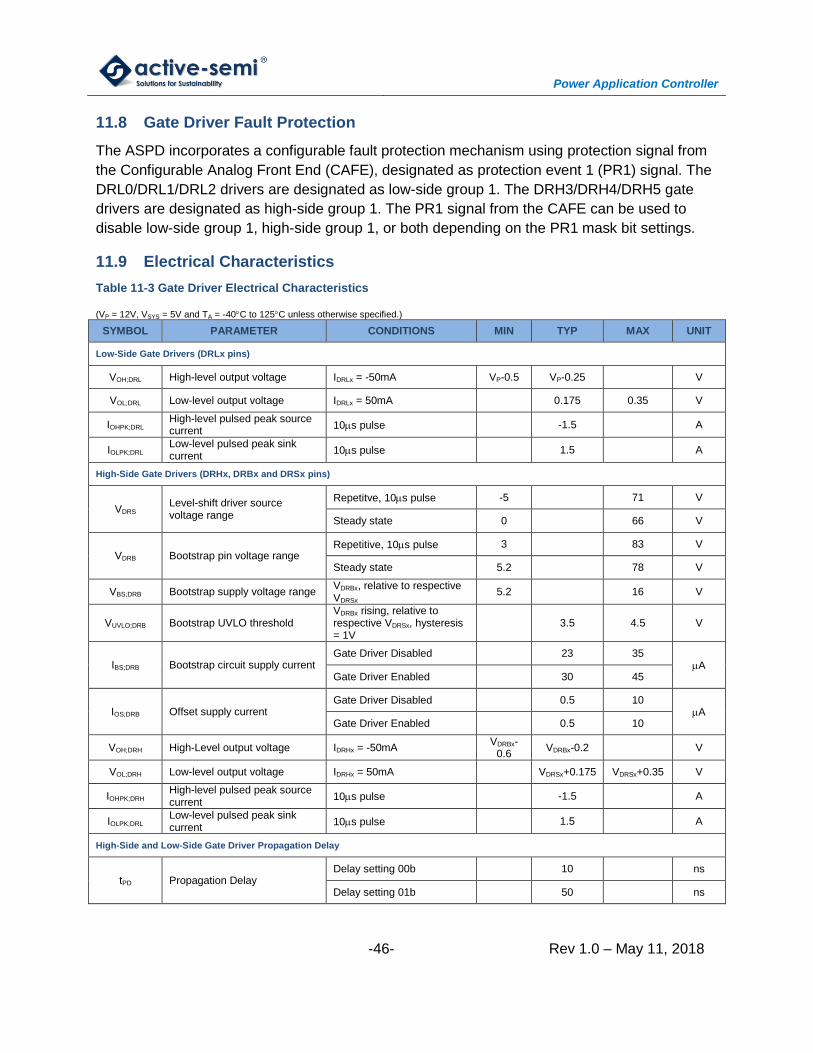
Power Application Controller
-46- Rev 1.0 – May 11, 2018
11.8 Gate Driver Fault Protection
The ASPD incorporates a configurable fault protection mechanism using protection signal from
the Configurable Analog Front End (CAFE), designated as protection event 1 (PR1) signal. The
DRL0/DRL1/DRL2 drivers are designated as low-side group 1. The DRH3/DRH4/DRH5 gate
drivers are designated as high-side group 1. The PR1 signal from the CAFE can be used to
disable low-side group 1, high-side group 1, or both depending on the PR1 mask bit settings.
11.9 Electrical Characteristics
Table 11-3 Gate Driver Electrical Characteristics
(VP = 12V, VSYS = 5V and TA = -40C to 125C unless otherwise specified.)
SYMBOL PARAMETER CONDITIONS MIN TYP MAX UNIT
Low-Side Gate Drivers (DRLx pins)
VOH;DRL High-level output voltage IDRLx = -50mA VP-0.5 VP-0.25 V
VOL;DRL Low-level output voltage IDRLx = 50mA 0.175 0.35 V
IOHPK;DRL High-level pulsed peak source current
10s pulse -1.5 A
IOLPK;DRL Low-level pulsed peak sink current
10s pulse 1.5 A
High-Side Gate Drivers (DRHx, DRBx and DRSx pins)
VDRS Level-shift driver source voltage range
Repetitve, 10s pulse -5 71 V
Steady state 0 66 V
VDRB Bootstrap pin voltage range Repetitive, 10s pulse 3 83 V
Steady state 5.2 78 V
VBS;DRB Bootstrap supply voltage range VDRBx, relative to respective VDRSx
5.2 16 V
VUVLO;DRB Bootstrap UVLO threshold VDRBx rising, relative to respective VDRSx, hysteresis = 1V
3.5 4.5 V
IBS;DRB Bootstrap circuit supply current Gate Driver Disabled 23 35
A Gate Driver Enabled 30 45
IOS;DRB Offset supply current Gate Driver Disabled 0.5 10
A Gate Driver Enabled 0.5 10
VOH;DRH High-Level output voltage IDRHx = -50mA VDRBx-
0.6 VDRBx-0.2 V
VOL;DRH Low-level output voltage IDRHx = 50mA VDRSx+0.175 VDRSx+0.35 V
IOHPK;DRH High-level pulsed peak source current
10s pulse -1.5 A
IOLPK;DRL Low-level pulsed peak sink current
10s pulse 1.5 A
High-Side and Low-Side Gate Driver Propagation Delay
tPD Propagation Delay Delay setting 00b 10 ns
Delay setting 01b 50 ns
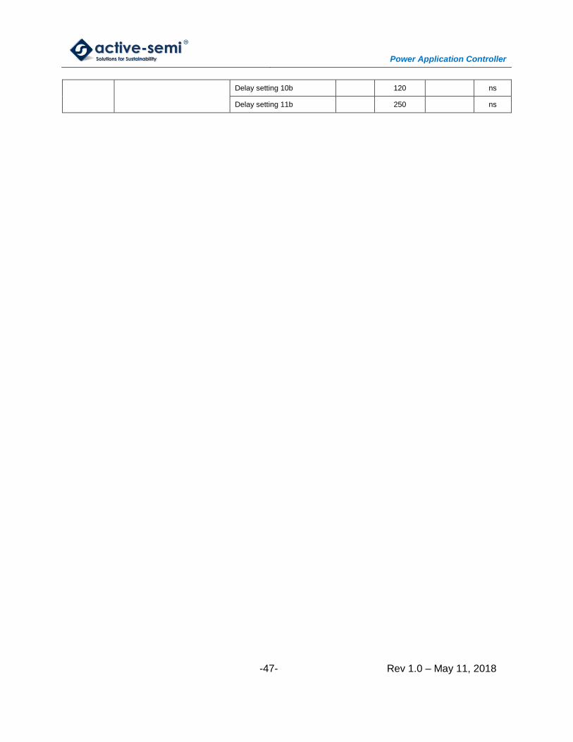
Power Application Controller
-47- Rev 1.0 – May 11, 2018
Delay setting 10b 120 ns
Delay setting 11b 250 ns
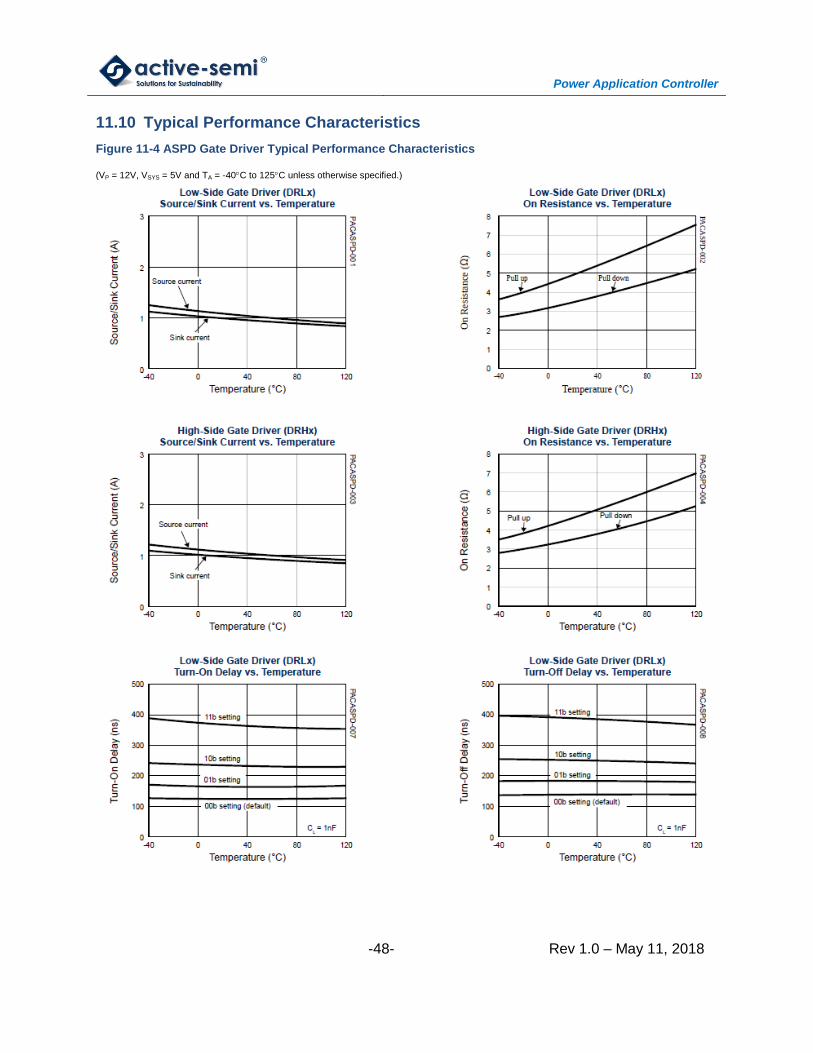
Power Application Controller
-48- Rev 1.0 – May 11, 2018
11.10 Typical Performance Characteristics
Figure 11-4 ASPD Gate Driver Typical Performance Characteristics
(VP = 12V, VSYS = 5V and TA = -40C to 125C unless otherwise specified.)
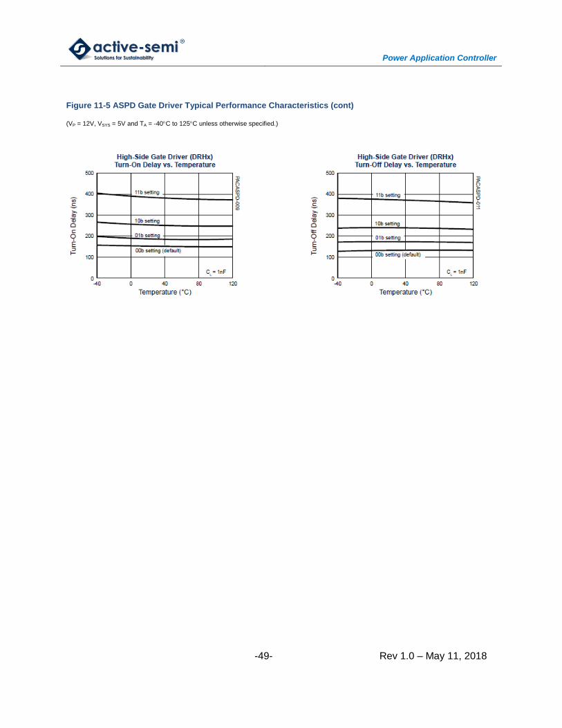
Power Application Controller
-49- Rev 1.0 – May 11, 2018
Figure 11-5 ASPD Gate Driver Typical Performance Characteristics (cont)
(VP = 12V, VSYS = 5V and TA = -40C to 125C unless otherwise specified.)
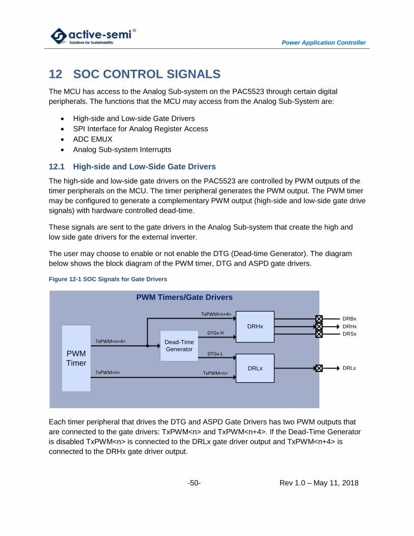
Power Application Controller
-50- Rev 1.0 – May 11, 2018
12 SOC CONTROL SIGNALS
The MCU has access to the Analog Sub-system on the PAC5523 through certain digital
peripherals. The functions that the MCU may access from the Analog Sub-System are:
High-side and Low-side Gate Drivers
SPI Interface for Analog Register Access
ADC EMUX
Analog Sub-system Interrupts
12.1 High-side and Low-Side Gate Drivers
The high-side and low-side gate drivers on the PAC5523 are controlled by PWM outputs of the
timer peripherals on the MCU. The timer peripheral generates the PWM output. The PWM timer
may be configured to generate a complementary PWM output (high-side and low-side gate drive
signals) with hardware controlled dead-time.
These signals are sent to the gate drivers in the Analog Sub-system that create the high and
low side gate drivers for the external inverter.
The user may choose to enable or not enable the DTG (Dead-time Generator). The diagram
below shows the block diagram of the PWM timer, DTG and ASPD gate drivers.
Figure 12-1 SOC Signals for Gate Drivers
PWM Timers/Gate Drivers
PWM
Timer
Dead-Time
Generator
TxPWM<n+4>
DRHx
DRLxTxPWM<n>
DRHx
DRSx
DRBx
DRLx
TxPWM<n+4>
DTGx-H
DTGx-L
TxPWM<n>
Each timer peripheral that drives the DTG and ASPD Gate Drivers has two PWM outputs that
are connected to the gate drivers: TxPWM<n> and TxPWM<n+4>. If the Dead-Time Generator
is disabled TxPWM<n> is connected to the DRLx gate driver output and TxPWM<n+4> is
connected to the DRHx gate driver output.
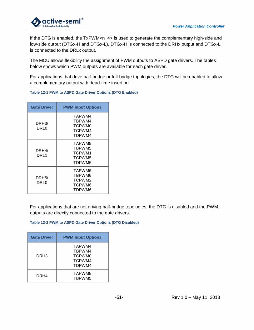
Power Application Controller
-51- Rev 1.0 – May 11, 2018
If the DTG is enabled, the TxPWM<n+4> is used to generate the complementary high-side and
low-side output (DTGx-H and DTGx-L). DTGx-H is connected to the DRHx output and DTGx-L
is connected to the DRLx output.
The MCU allows flexibility the assignment of PWM outputs to ASPD gate drivers. The tables
below shows which PWM outputs are available for each gate driver.
For applications that drive half-bridge or full-bridge topologies, the DTG will be enabled to allow
a complementary output with dead-time insertion.
Table 12-1 PWM to ASPD Gate Driver Options (DTG Enabled)
Gate Driver PWM Input Options
DRH3/ DRL0
TAPWM4 TBPWM4 TCPWM0 TCPWM4 TDPWM4
DRH4/ DRL1
TAPWM5 TBPWM5 TCPWM1 TCPWM5 TDPWM5
DRH5/ DRL0
TAPWM6 TBPWM6 TCPWM2 TCPWM6 TDPWM6
For applications that are not driving half-bridge topologies, the DTG is disabled and the PWM
outputs are directly connected to the gate drivers.
Table 12-2 PWM to ASPD Gate Driver Options (DTG Disabled)
Gate Driver PWM Input Options
DRH3
TAPWM4 TBPWM4 TCPWM0 TCPWM4 TDPWM4
DRH4 TAPWM5 TBPWM5
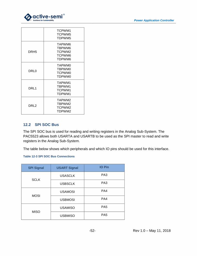
Power Application Controller
-52- Rev 1.0 – May 11, 2018
TCPWM1 TCPWM5 TDPWM5
DRH5
TAPWM6 TBPWM6 TCPWM2 TCPWM6 TDPWM6
DRL0
TAPWM0 TBPWM0 TCPWM0 TDPWM0
DRL1
TAPWM1 TBPWM1 TCPWM1 TDPWM1
DRL2
TAPWM2 TBPWM2 TCPWM2 TDPWM2
12.2 SPI SOC Bus
The SPI SOC bus is used for reading and writing registers in the Analog Sub-System. The
PAC5523 allows both USARTA and USARTB to be used as the SPI master to read and write
registers in the Analog Sub-System.
The table below shows which peripherals and which IO pins should be used for this interface.
Table 12-3 SPI SOC Bus Connections
SPI Signal USART Signal IO Pin
SCLK
USASCLK PA3
USBSCLK PA3
MOSI
USAMOSI PA4
USBMOSI PA4
MISO
USAMISO PA5
USBMISO PA5
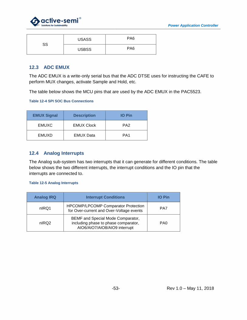
Power Application Controller
-53- Rev 1.0 – May 11, 2018
SS
USASS PA6
USBSS PA6
12.3 ADC EMUX
The ADC EMUX is a write-only serial bus that the ADC DTSE uses for instructing the CAFE to
perform MUX changes, activate Sample and Hold, etc.
The table below shows the MCU pins that are used by the ADC EMUX in the PAC5523.
Table 12-4 SPI SOC Bus Connections
EMUX Signal Description IO Pin
EMUXC EMUX Clock PA2
EMUXD EMUX Data PA1
12.4 Analog Interrupts
The Analog sub-system has two interrupts that it can generate for different conditions. The table
below shows the two different interrupts, the interrupt conditions and the IO pin that the
interrupts are connected to.
Table 12-5 Analog Interrupts
Analog IRQ Interrupt Conditions IO Pin
nIRQ1 HPCOMP/LPCOMP Comparator Protection for Over-current and Over-Voltage events
PA7
nIRQ2 BEMF and Special Mode Comparator, including phase to phase comparator,
AIO6/AIO7/AIO8/AIO9 interrupt PA0
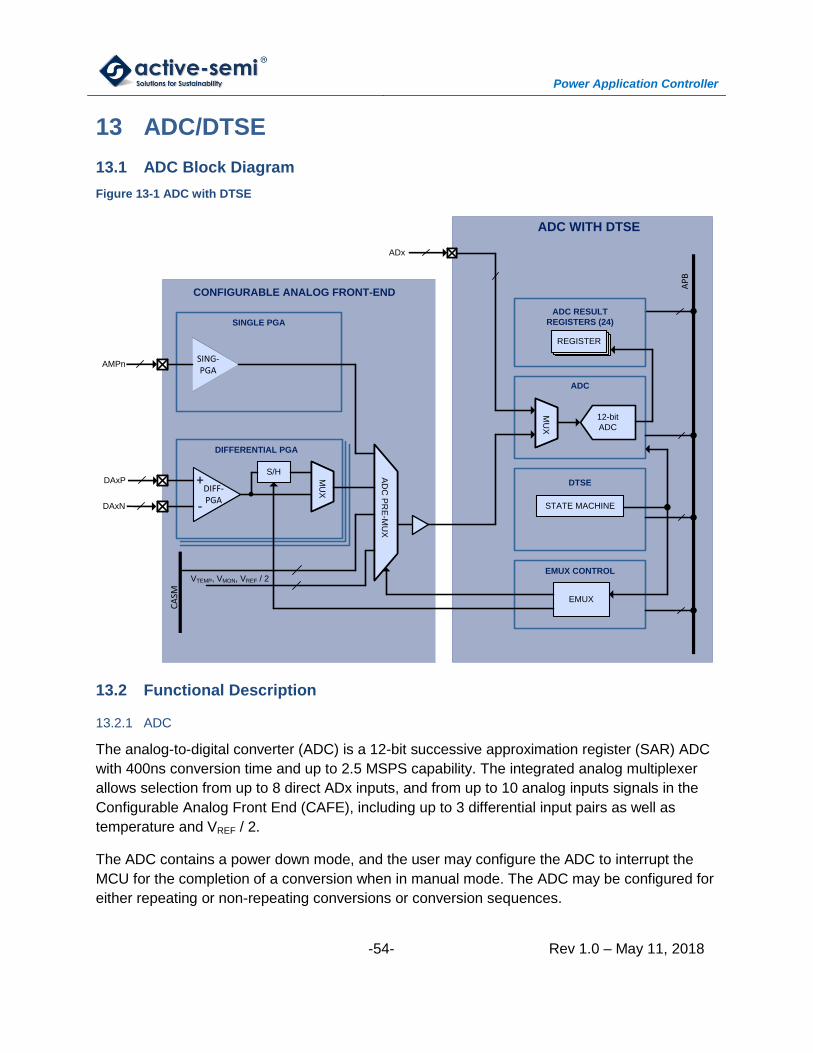
Power Application Controller
-54- Rev 1.0 – May 11, 2018
13 ADC/DTSE
13.1 ADC Block Diagram
Figure 13-1 ADC with DTSE
REGISTERREGISTER
ADx
DAxP
ADC RESULT
REGISTERS (24)
REGISTER
ADC WITH DTSE
AP
B
ADC
DTSE
EMUX CONTROL
12-bit
ADC
MU
XM
UX
STATE MACHINE
EMUX
AD
C P
RE
-MU
XA
DC
PR
E-M
UX
MU
XM
UX
S/H
DIFFERENTIAL PGA
VTEMP, VMON, VREF / 2
-
+
-
+
CA
SM
DAxN
SINGLE PGA
DIFF-PGA
SING-PGA
AMPn
CONFIGURABLE ANALOG FRONT-END
13.2 Functional Description
13.2.1 ADC
The analog-to-digital converter (ADC) is a 12-bit successive approximation register (SAR) ADC
with 400ns conversion time and up to 2.5 MSPS capability. The integrated analog multiplexer
allows selection from up to 8 direct ADx inputs, and from up to 10 analog inputs signals in the
Configurable Analog Front End (CAFE), including up to 3 differential input pairs as well as
temperature and VREF / 2.
The ADC contains a power down mode, and the user may configure the ADC to interrupt the
MCU for the completion of a conversion when in manual mode. The ADC may be configured for
either repeating or non-repeating conversions or conversion sequences.
Power Application Controller
-55- Rev 1.0 – May 11, 2018
13.2.2 Dynamic Triggering and Sample Engine
The Dynamic Triggering and Sample Engine (DTSE) is a highly-configurable automatic
sequencer that allows the user to configure automatic sampling of their application-specific
analog signals without any interaction from the micro-controller core. The DTSE also contains a
pseudo-DMA engine that copies each of up to 24 conversion results to dedicated memory
space and can interrupt the MCU when complete.
The DTSE has up to 32 input triggers, from PWM Timers A, B, C and D for either the rising,
falling or rising and falling PWM edges. The user may also force any trigger sequence by writing
a register via firmware. The user can configure the DTSE to chain from 1 to 24 conversions to
any PWM trigger.
The DTSE has a flexible interrupt structure that allows up to 24 interrupts to be configured at the
completion of any individual conversion. The user may configure one of four different IRQ
signals wen generating an interrupt during sequence conversions. The IRQ may be generated
at the end of a conversion sequence, or at the end of series of conversions. The user may
select one of four IRQs for conversions, and each may be assigned a different interrupt priority.
Each of the 24 conversions has dedicated results registers, so that the pseudo-DMA engine has
dedicated storage for each of the conversion results.
13.2.3 EMUX Control
A dedicated low latency interface controllable by the DTSE or register control allows changing
the ADC pre-multiplexer and asserting/de-asserting the S/H circuit in the Configurable Analog
Front-End (CAFE), allowing back to back conversions of multiple analog inputs without
microcontroller interaction.
For more information on the ADC and DTSE, see the PAC55XX Family User Guide.
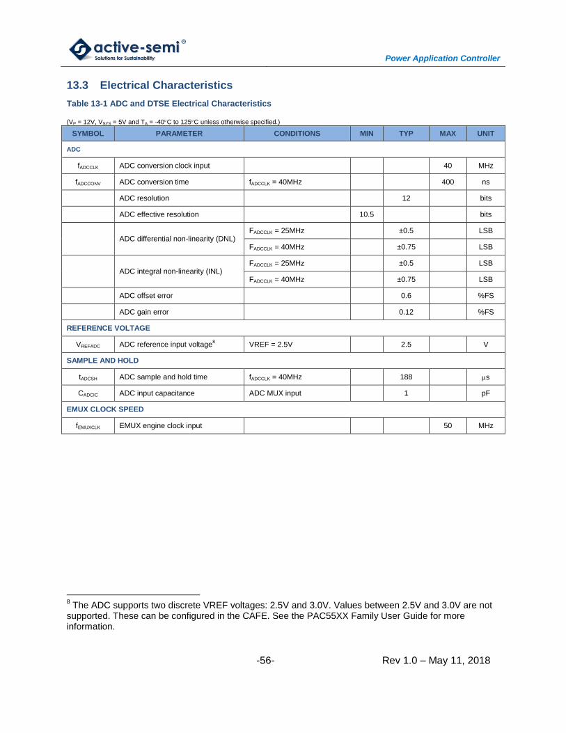
Power Application Controller
-56- Rev 1.0 – May 11, 2018
13.3 Electrical Characteristics
Table 13-1 ADC and DTSE Electrical Characteristics
(VP = 12V, VSYS = 5V and TA = -40C to 125C unless otherwise specified.)
SYMBOL PARAMETER CONDITIONS MIN TYP MAX UNIT
ADC
fADCCLK ADC conversion clock input 40 MHz
fADCCONV ADC conversion time fADCCLK = 40MHz 400 ns
ADC resolution 12 bits
ADC effective resolution 10.5 bits
ADC differential non-linearity (DNL) FADCCLK = 25MHz ±0.5 LSB
FADCCLK = 40MHz ±0.75 LSB
ADC integral non-linearity (INL) FADCCLK = 25MHz ±0.5 LSB
FADCCLK = 40MHz ±0.75 LSB
ADC offset error 0.6 %FS
ADC gain error 0.12 %FS
REFERENCE VOLTAGE
VREFADC ADC reference input voltage8 VREF = 2.5V 2.5 V
SAMPLE AND HOLD
tADCSH ADC sample and hold time fADCCLK = 40MHz 188 s
CADCIC ADC input capacitance ADC MUX input 1 pF
EMUX CLOCK SPEED
fEMUXCLK EMUX engine clock input 50 MHz
8 The ADC supports two discrete VREF voltages: 2.5V and 3.0V. Values between 2.5V and 3.0V are not
supported. These can be configured in the CAFE. See the PAC55XX Family User Guide for more information.
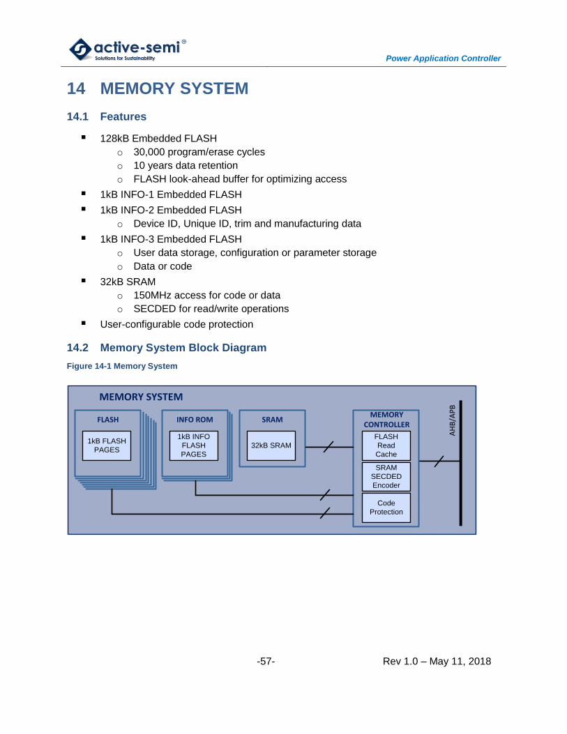
Power Application Controller
-57- Rev 1.0 – May 11, 2018
14 MEMORY SYSTEM
14.1 Features
128kB Embedded FLASH
o 30,000 program/erase cycles
o 10 years data retention
o FLASH look-ahead buffer for optimizing access
1kB INFO-1 Embedded FLASH
1kB INFO-2 Embedded FLASH
o Device ID, Unique ID, trim and manufacturing data
1kB INFO-3 Embedded FLASH
o User data storage, configuration or parameter storage
o Data or code
32kB SRAM
o 150MHz access for code or data
o SECDED for read/write operations
User-configurable code protection
14.2 Memory System Block Diagram
Figure 14-1 Memory System
AH
B/A
PB
FLASH
1kB FLASH
PAGES
SRAM
32kB SRAM
MEMORY SYSTEM
MEMORYCONTROLLER
FLASH
Read
Cache
SRAM
SECDED
Encoder
Code
Protection
INFO ROM
1kB INFO
FLASH
PAGESA
HB
/AP
B
FLASH
1kB FLASH
PAGES
SRAM
32kB SRAM
MEMORY SYSTEM
MEMORYCONTROLLER
FLASH
Read
Cache
SRAM
SECDED
Encoder
Code
Protection
INFO ROM
1kB INFO
FLASH
PAGES
Power Application Controller
-58- Rev 1.0 – May 11, 2018
14.3 Functional Description
The PAC55XX has multiple banks of embedded FLASH memory, SRAM memory as well as
peripheral control registers that are program-accessible in a flat memory map.
14.4 Program FLASH
The PAC55XX Memory Controller provides access to 128 1kB pages of main program FLASH
for a total of 128kB of FLASH through the system AHB bus. Each page may be individually
erased or written while the MCU is executing instructions from SRAM or from INFO-2 or INFO-3
FLASH memory.
The PAC55XX Memory Controller provides a FLASH read buffer that optimizes access from the
MCU to the FLASH memory. This look ahead buffer monitors the program execution and
fetches instructions from FLASH before they are needed to optimize access to this memory.
14.5 INFO FLASH
The PAC55XX Memory Controller provides access to the INFO-1, INFO-2 and INFO-3 FLASH
memories, which are each a single 1kB page for a total of 3kB or memory.
INFO-1 and INFO-2 are read-only memories that contains device-specific information such as
the device ID, a unique ID, trimming and calibration data that may be used by programs
executing on the PAC55XX.
INFO-3 is available to the user for data or program storage.
14.6 SRAM
The PAC55XX Memory Controller provides access to the 32kB SRAM for non-persistent data
storage. The SRAM memory supports word (4B), half-word (2B) and byte addresses with
aligned access.
The PAC55XX Memory Controller can read or write data from RAM up to 150MHz. This can be
a benefit for time-critical applications. This memory can also be used for program execution
when modifying the contents of FLASH, INFO-1 or INFO-2 FLASH.
The PAC55XX Memory Controller also has an SECDED encoder, capable of detecting and
correcting single-bit errors, and detecting double-bit errors. The user may read the status of the
encoder, to see if a single-bit error has occurred. The user may also enable an interrupt upon
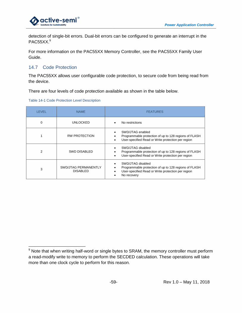
Power Application Controller
-59- Rev 1.0 – May 11, 2018
detection of single-bit errors. Dual-bit errors can be configured to generate an interrupt in the
PAC55XX.9
For more information on the PAC55XX Memory Controller, see the PAC55XX Family User
Guide.
14.7 Code Protection
The PAC55XX allows user configurable code protection, to secure code from being read from
the device.
There are four levels of code protection available as shown in the table below.
Table 14-1 Code Protection Level Description
LEVEL NAME FEATURES
0 UNLOCKED No restrictions
1 RW PROTECTION
SWD/JTAG enabled
Programmable protection of up to 128 regions of FLASH
User-specified Read or Write protection per region
2 SWD DISABLED
SWD/JTAG disabled
Programmable protection of up to 128 regions of FLASH
User-specified Read or Write protection per region
3 SWD/JTAG PERMANENTLY
DISABLED
SWD/JTAG disabled
Programmable protection of up to 128 regions of FLASH
User-specified Read or Write protection per region
No recovery
9 Note that when writing half-word or single bytes to SRAM, the memory controller must perform
a read-modify write to memory to perform the SECDED calculation. These operations will take
more than one clock cycle to perform for this reason.
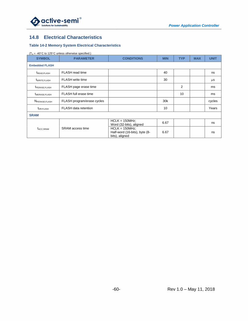
Power Application Controller
-60- Rev 1.0 – May 11, 2018
14.8 Electrical Characteristics
Table 14-2 Memory System Electrical Characteristics
(TA = -40C to 125C unless otherwise specified.)
SYMBOL PARAMETER CONDITIONS MIN TYP MAX UNIT
Embedded FLASH
tREAD;FLASH FLASH read time 40 ns
tWRITE;FLASH FLASH write time 30 s
tPERASE;FLASH FLASH page erase time 2 ms
tMERASE;FLASH FLASH full erase time 10 ms
NPERASE;FLASH FLASH program/erase cycles 30k cycles
tDR;FLASH FLASH data retention 10 Years
SRAM
tACC;SRAM SRAM access time
HCLK = 150MHz; Word (32-bits), aligned
6.67 ns
HCLK = 150MHz; Half-word (16-bits), byte (8-bits), aligned
6.67 ns
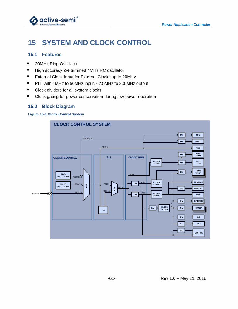
Power Application Controller
-61- Rev 1.0 – May 11, 2018
15 SYSTEM AND CLOCK CONTROL
15.1 Features
20MHz Ring Oscillator
High accuracy 2% trimmed 4MHz RC oscillator
External Clock Input for External Clocks up to 20MHz
PLL with 1MHz to 50MHz input, 62.5MHz to 300MHz output
Clock dividers for all system clocks
Clock gating for power conservation during low-power operation
15.2 Block Diagram
Figure 15-1 Clock Control System
RTC
RING
OSCILLATOR
2% RC
OSCILLATOR
CLOCK SOURCES
MU
X
EXTCLK
PLL
PLL
MU
X
CLOCK TREE
DIV
ACLK
PC
LK
CLOCK
GATING
CLOCK
GATING
DIV
DIV
DIV
DIV
DIV
DIV
DIV
CLOCK CONTROL SYSTEM
ROSCCLK
REFCLK
EXTCLK
SCLK
PLLCLK
FRCLK DIV
DIV
SCLK
HCLK
CLOCK
GATING
CLOCK
GATING
WWDT
WIC
ADC/
DTSE
PWM
TIMER
ARM MCU
MEMCTL
CRC
GPTIMER
ADC
EMUX
USART
I2C
CAN
SYSTICK
DIV
DIV
DIV
DIV
ROSCCLK
FRCLK
Power Application Controller
-62- Rev 1.0 – May 11, 2018
15.3 Clock Sources
15.3.1 Ring Oscillator
The Ring Oscillator (ROSC) is an integrated 20MHz clock oscillator that is the default system
clock, and is available by default when the PAC55XX comes out of reset. The output of the
ROSC is the ROSCCLK clock. The ROSCLK may be selected as the FRCLK clock and may
supply the WWDT, for applications that need an independent clock source or need to continue
to be clocked when the system is in a low-power mode.
The ROSC may be disabled by the user by a configuration register.
15.3.2 Reference Clock
The Reference Clock (REFCLK) is an integrated 2% trimmed 4MHz RC clock. This clock is
suitable for many applications. This clock may be selected as the FRCLK and can be used as
the input to the PLL and is used to derive the clock for the MMPM.
15.3.3 External Clock Input
The External Clock Input (EXTCLK) is a clock input available through the digital peripheral
MUX, and allows the drive the clock system by a 50% duty cycle clock of up to 20MHz. This
clock may be selected as FRCLK and can be used as the input the PLL (as long as the
accuracy is better than +/- 2%).
15.4 PLL
The PAC55XX contains a Phase Lock Loop (PLL) that can generate very high clock frequencies
up to 300MHz for the peripherals and timers in the device. The input to the PLL is the FRCLK
and must be from the EXTCLK or REFCLK clock sources
The input to the PLL must be between 1MHz – 50MHz and the output can be configured to be
from 62.5MHz to 300MHz. The user can configure the PLL to generate the desired clock output
based on a set of configuration registers in the CCS. The output of the PLL is the PLLCLK
clock. The user may configure a MUX to generate the SCLK clock from PLLCLK or from
FRCLK.
In addition to configuring the PLL output frequency, the PLL may be enabled, disabled and
bypassed through a set of configuration registers in the CCS.
15.5 Clock Tree
The following are of the system clocks available in the clock tree. See the section below to see
which clocks are available for each of the digital peripherals in the system.
Power Application Controller
-63- Rev 1.0 – May 11, 2018
15.5.1 FRCLK
The free-running clock (FRCLK) is generated from one of the four clock sources (ROSCCLK,
EXTCLK or REFCLK). This clock may be used by the WWDT and the RTC, for configurations
that turn off all other system clocks during low power operation.
The FRCLK or PLLCLK is selected via a MUX and the output becomes SCLK.
15.5.2 SCLK
The System Clock (SCLK) generates two system clocks: ACLK and HCLK. Each of these
system clocks has their own 3b clock divider and is described below.
15.5.3 PCLK
The Peripheral Clock (PCLK) is used by most of the digital peripherals in the PAC55XX. This
clock has a 3b clock divider and also has clock gating support, which allows this clock output to
be disabled before the system is put into the ARM Cortex-M4’s deep sleep mode to conserve
energy.
As shown above, most of the peripherals that use PCLK also have their own clock dividers so
that this clock can be further divided down to meet the application’s needs.
15.5.4 ACLK
The Auxiliary Clock (ACLK) may be optionally used by the PWM timer block in the PAC55XX in
order to generate a very fast clock for PWM output to generate the best possible accuracy and
edge generation.
This clock has a 3b clock divider and also has clock gating support, which disables this clock
output when the system is put into the ARM Cortex-M4’s deep sleep mode to conserve energy.
As shown above, the ACLK is an optional input for just the PWM timer block in the PAC55XX.
15.5.5 HCLK
The AHB Clock (HCLK) is used by the ARM Cortex-M4 MCU and Memory Controller peripheral.
This clock has a 3b divider and also has clock gating support, which allows this clock output to
be disabled before the system is put into the ARM Cortex-M4’s deep sleep mode to conserve
energy.
HCLK supplies PCLK with its clock source.
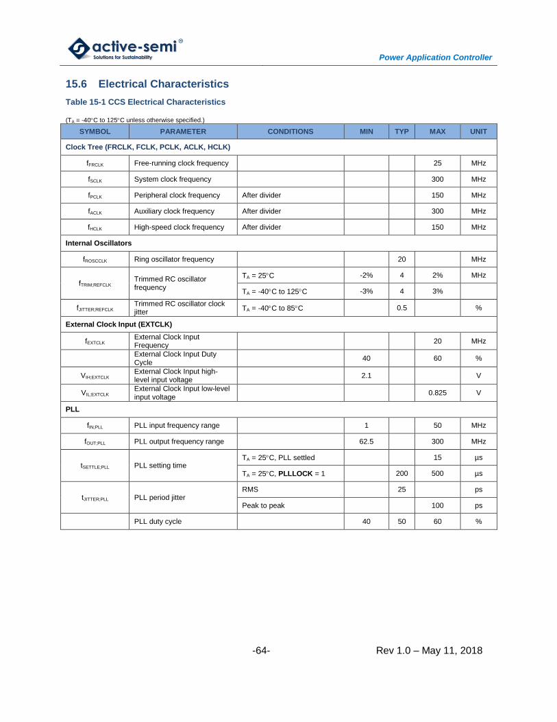
Power Application Controller
-64- Rev 1.0 – May 11, 2018
15.6 Electrical Characteristics
Table 15-1 CCS Electrical Characteristics
(TA = -40C to 125C unless otherwise specified.)
SYMBOL PARAMETER CONDITIONS MIN TYP MAX UNIT
Clock Tree (FRCLK, FCLK, PCLK, ACLK, HCLK)
fFRCLK Free-running clock frequency 25 MHz
fSCLK System clock frequency 300 MHz
fPCLK Peripheral clock frequency After divider 150 MHz
fACLK Auxiliary clock frequency After divider 300 MHz
fHCLK High-speed clock frequency After divider 150 MHz
Internal Oscillators
fROSCCLK Ring oscillator frequency 20 MHz
fTRIM;REFCLK Trimmed RC oscillator frequency
TA = 25C -2% 4 2% MHz
TA = -40C to 125C -3% 4 3%
fJITTER;REFCLK Trimmed RC oscillator clock jitter
TA = -40C to 85C 0.5 %
External Clock Input (EXTCLK)
fEXTCLK External Clock Input Frequency
20 MHz
External Clock Input Duty Cycle
40 60 %
VIH;EXTCLK External Clock Input high-level input voltage
2.1 V
VIL;EXTCLK External Clock Input low-level input voltage
0.825 V
PLL
fIN;PLL PLL input frequency range 1 50 MHz
fOUT;PLL PLL output frequency range 62.5 300 MHz
tSETTLE;PLL PLL setting time TA = 25C, PLL settled 15 µs
TA = 25C, PLLLOCK = 1 200 500 µs
tJITTER;PLL PLL period jitter RMS 25 ps
Peak to peak 100 ps
PLL duty cycle 40 50 60 %
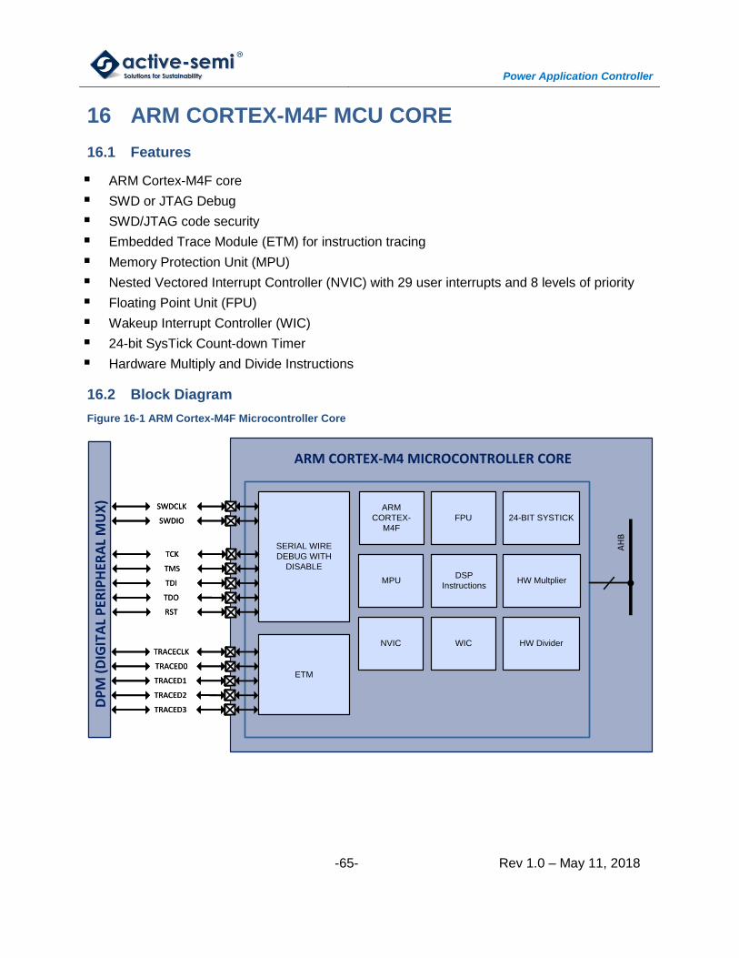
Power Application Controller
-65- Rev 1.0 – May 11, 2018
16 ARM CORTEX-M4F MCU CORE
16.1 Features
ARM Cortex-M4F core
SWD or JTAG Debug
SWD/JTAG code security
Embedded Trace Module (ETM) for instruction tracing
Memory Protection Unit (MPU)
Nested Vectored Interrupt Controller (NVIC) with 29 user interrupts and 8 levels of priority
Floating Point Unit (FPU)
Wakeup Interrupt Controller (WIC)
24-bit SysTick Count-down Timer
Hardware Multiply and Divide Instructions
16.2 Block Diagram
Figure 16-1 ARM Cortex-M4F Microcontroller Core
AH
B
MPUDSP
InstructionsHW Multplier
ARM CORTEX-M4 MICROCONTROLLER CORE
ARM
CORTEX-
M4F
FPU 24-BIT SYSTICK
NVIC WIC HW Divider
SERIAL WIRE
DEBUG WITH
DISABLE
ETM
TRACECLK
TRACED0
TRACED1
TRACED2
TRACED3
DP
M (
DIG
ITA
L P
ERIP
HER
AL
MU
X)
TCK
TMS
TDI
TDO
RST
SWDCLK
SWDIO
AH
B
MPUDSP
InstructionsHW Multplier
ARM CORTEX-M4 MICROCONTROLLER CORE
ARM
CORTEX-
M4F
FPU 24-BIT SYSTICK
NVIC WIC HW Divider
SERIAL WIRE
DEBUG WITH
DISABLE
ETM
TRACECLK
TRACED0
TRACED1
TRACED2
TRACED3
DP
M (
DIG
ITA
L P
ERIP
HER
AL
MU
X)
TCK
TMS
TDI
TDO
RST
SWDCLK
SWDIO
Power Application Controller
-66- Rev 1.0 – May 11, 2018
16.3 Functional Description
The ARM Cortex-M4F microcontroller core is configured for little endian operation and includes
hardware support for multiplication and division, DSP instructions as well as an IEEE754 single-
precision Floating Point Unit (FPU).
The MCU also contains an 8-region Memory Protection Unit (MPU), as well as a Nested Vector
Interrupt Controller (NVIC) that supports 29 user interrupts with 8 levels of priority. There is a
24-bit SysTick count-down timer.
The ARM Cortex-M4F supports sleep and deep sleep modes for low power operation. In sleep
mode, the ARM Cortex-M4F is disabled. In deep sleep mode, the MCU as well as many
peripherals are disabled. The Wakeup Interrupt Controller (WIC) can wake up the MCU when in
deep sleep mode by using any GPIO interrupt, the Real-Time Clock (RTC) or Windowed
Watchdog Timer (WWDT). The PAC55XX also supports clock gating to reduce power during
deep sleep operation.
The debugger supports 4 breakpoint and 2 watch-point unit comparators using the SWD or
JTAG protocols. The debug serial interfaces may be disabled to prevent memory access to the
firmware during customer production.
For more information on the detailed operation of the Microcontroller Core in the PAC55XX, see
the PAC55XX Family User Guide.
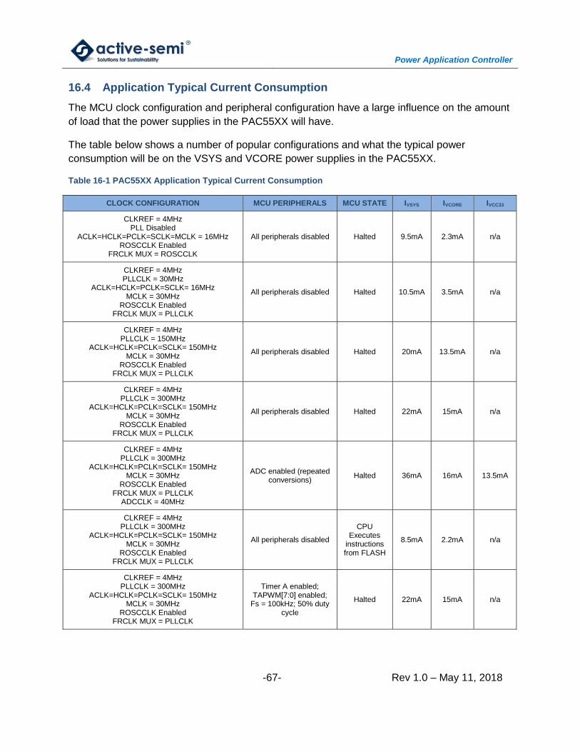
Power Application Controller
-67- Rev 1.0 – May 11, 2018
16.4 Application Typical Current Consumption
The MCU clock configuration and peripheral configuration have a large influence on the amount
of load that the power supplies in the PAC55XX will have.
The table below shows a number of popular configurations and what the typical power
consumption will be on the VSYS and VCORE power supplies in the PAC55XX.
Table 16-1 PAC55XX Application Typical Current Consumption
CLOCK CONFIGURATION MCU PERIPHERALS MCU STATE IVSYS IVCORE IVCC33
CLKREF = 4MHz PLL Disabled
ACLK=HCLK=PCLK=SCLK=MCLK = 16MHz ROSCCLK Enabled
FRCLK MUX = ROSCCLK
All peripherals disabled Halted 9.5mA 2.3mA n/a
CLKREF = 4MHz PLLCLK = 30MHz
ACLK=HCLK=PCLK=SCLK= 16MHz MCLK = 30MHz
ROSCCLK Enabled FRCLK MUX = PLLCLK
All peripherals disabled Halted 10.5mA 3.5mA n/a
CLKREF = 4MHz PLLCLK = 150MHz
ACLK=HCLK=PCLK=SCLK= 150MHz MCLK = 30MHz
ROSCCLK Enabled FRCLK MUX = PLLCLK
All peripherals disabled Halted 20mA 13.5mA n/a
CLKREF = 4MHz PLLCLK = 300MHz
ACLK=HCLK=PCLK=SCLK= 150MHz MCLK = 30MHz
ROSCCLK Enabled FRCLK MUX = PLLCLK
All peripherals disabled Halted 22mA 15mA n/a
CLKREF = 4MHz PLLCLK = 300MHz
ACLK=HCLK=PCLK=SCLK= 150MHz MCLK = 30MHz
ROSCCLK Enabled FRCLK MUX = PLLCLK
ADCCLK = 40MHz
ADC enabled (repeated conversions)
Halted 36mA 16mA 13.5mA
CLKREF = 4MHz PLLCLK = 300MHz
ACLK=HCLK=PCLK=SCLK= 150MHz MCLK = 30MHz
ROSCCLK Enabled FRCLK MUX = PLLCLK
All peripherals disabled
CPU Executes
instructions from FLASH
8.5mA 2.2mA n/a
CLKREF = 4MHz PLLCLK = 300MHz
ACLK=HCLK=PCLK=SCLK= 150MHz MCLK = 30MHz
ROSCCLK Enabled FRCLK MUX = PLLCLK
Timer A enabled; TAPWM[7:0] enabled;
Fs = 100kHz; 50% duty cycle
Halted 22mA 15mA n/a
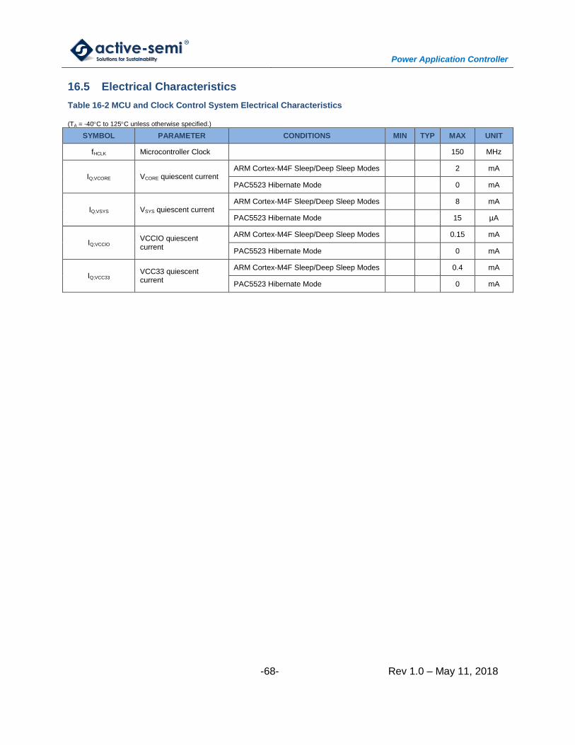
Power Application Controller
-68- Rev 1.0 – May 11, 2018
16.5 Electrical Characteristics
Table 16-2 MCU and Clock Control System Electrical Characteristics
(TA = -40C to 125C unless otherwise specified.)
SYMBOL PARAMETER CONDITIONS MIN TYP MAX UNIT
fHCLK Microcontroller Clock 150 MHz
IQ;VCORE VCORE quiescent current ARM Cortex-M4F Sleep/Deep Sleep Modes 2 mA
PAC5523 Hibernate Mode 0 mA
IQ;VSYS VSYS quiescent current ARM Cortex-M4F Sleep/Deep Sleep Modes 8 mA
PAC5523 Hibernate Mode 15 µA
IQ;VCCIO VCCIO quiescent current
ARM Cortex-M4F Sleep/Deep Sleep Modes 0.15 mA
PAC5523 Hibernate Mode 0 mA
IQ;VCC33 VCC33 quiescent current
ARM Cortex-M4F Sleep/Deep Sleep Modes 0.4 mA
PAC5523 Hibernate Mode 0 mA
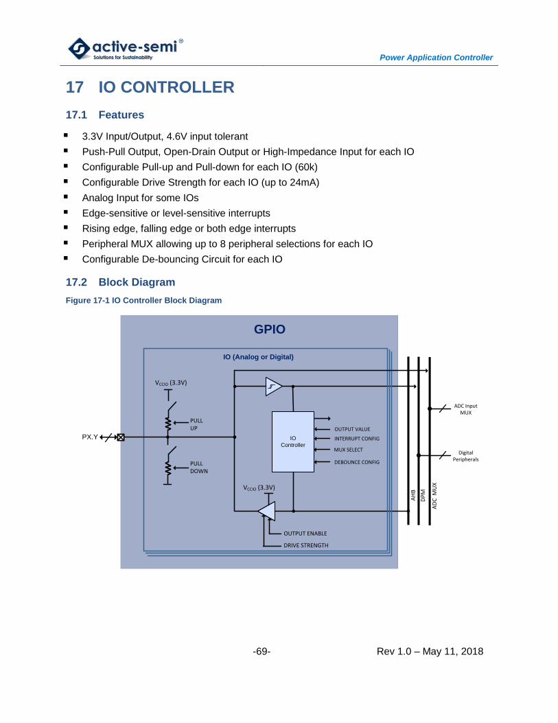
Power Application Controller
-69- Rev 1.0 – May 11, 2018
17 IO CONTROLLER
17.1 Features
3.3V Input/Output, 4.6V input tolerant
Push-Pull Output, Open-Drain Output or High-Impedance Input for each IO
Configurable Pull-up and Pull-down for each IO (60k)
Configurable Drive Strength for each IO (up to 24mA)
Analog Input for some IOs
Edge-sensitive or level-sensitive interrupts
Rising edge, falling edge or both edge interrupts
Peripheral MUX allowing up to 8 peripheral selections for each IO
Configurable De-bouncing Circuit for each IO
17.2 Block Diagram
Figure 17-1 IO Controller Block Diagram
VCCIO (3.3V)
VCCIO (3.3V)
OUTPUT ENABLE
PULLUP
IO (Analog or Digital)
PX.Y
GPIO
DRIVE STRENGTH
IO
Controller
AD
C M
UX
PULLDOWN
ADC Input MUX
OUTPUT VALUE
INTERRUPT CONFIG
MUX SELECT
DEBOUNCE CONFIG
DP
M
AH
B
DigitalPeripherals
Power Application Controller
-70- Rev 1.0 – May 11, 2018
17.3 Functional Description
The PAC55XX IO cells can be used for digital input/output and analog input for the ADC. All IOs
are supplied by the VCCIO (3.3V) power supply.
Each IO can be configured for digital push-pull output, open-drain output or high-impedance
input. Each IO also has a configurable 60k weak pull-up or weak pull-down that can be enabled.
NOTE: Configuring both pull-up and pull-down at the same time may cause device
damage and should be avoided.
Each IO has a configurable de-bouncing filter that can be enabled or disabled, to help filter out
noise.
All IO have interrupt capability. Each pin can be configured for either level or edge sensitive
interrupts, and can select between rising edge, falling edge and both edges for interrupts. Each
pin has a separate interrupt enable and interrupt flag.
Some of the IO on the PAC5523 can be configured as an analog input to the ADC.
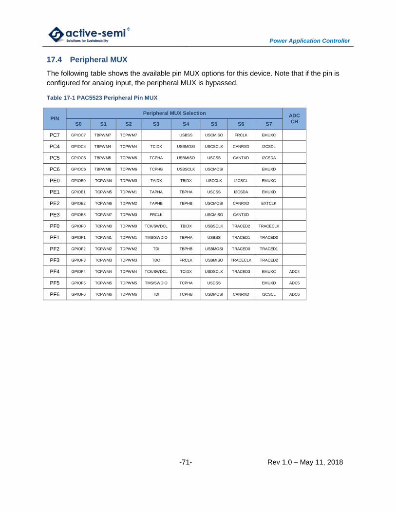
Power Application Controller
-71- Rev 1.0 – May 11, 2018
17.4 Peripheral MUX
The following table shows the available pin MUX options for this device. Note that if the pin is
configured for analog input, the peripheral MUX is bypassed.
Table 17-1 PAC5523 Peripheral Pin MUX
PIN Peripheral MUX Selection ADC
CH S0 S1 S2 S3 S4 S5 S6 S7
PC7 GPIOC7 TBPWM7 TCPWM7 USBSS USCMISO FRCLK EMUXC
PC4 GPIOC4 TBPWM4 TCPWM4 TCIDX USBMOSI USCSCLK CANRXD I2CSDL
PC5 GPIOC5 TBPWM5 TCPWM5 TCPHA USBMISO USCSS CANTXD I2CSDA
PC6 GPIOC6 TBPWM6 TCPWM6 TCPHB USBSCLK USCMOSI EMUXD
PE0 GPIOE0 TCPWM4 TDPWM0 TAIDX TBIDX USCCLK I2CSCL EMUXC
PE1 GPIOE1 TCPWM5 TDPWM1 TAPHA TBPHA USCSS I2CSDA EMUXD
PE2 GPIOE2 TCPWM6 TDPWM2 TAPHB TBPHB USCMOSI CANRXD EXTCLK
PE3 GPIOE3 TCPWM7 TDPWM3 FRCLK USCMISO CANTXD
PF0 GPIOF0 TCPWM0 TDPWM0 TCK/SWDCL TBIDX USBSCLK TRACED2 TRACECLK
PF1 GPIOF1 TCPWM1 TDPWM1 TMS/SWDIO TBPHA USBSS TRACED1 TRACED0
PF2 GPIOF2 TCPWM2 TDPWM2 TDI TBPHB USBMOSI TRACED0 TRACED1
PF3 GPIOF3 TCPWM3 TDPWM3 TDO FRCLK USBMISO TRACECLK TRACED2
PF4 GPIOF4 TCPWM4 TDPWM4 TCK/SWDCL TCIDX USDSCLK TRACED3 EMUXC ADC4
PF5 GPIOF5 TCPWM5 TDPWM5 TMS/SWDIO TCPHA USDSS EMUXD ADC5
PF6 GPIOF6 TCPWM6 TDPWM6 TDI TCPHB USDMOSI CANRXD I2CSCL ADC6
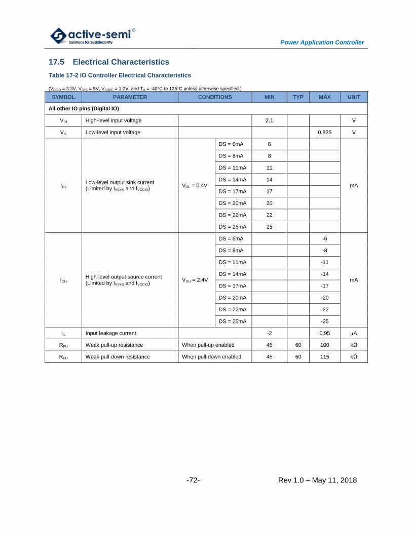
Power Application Controller
-72- Rev 1.0 – May 11, 2018
17.5 Electrical Characteristics
Table 17-2 IO Controller Electrical Characteristics
(VCCIO = 3.3V, VSYS = 5V, VCORE = 1.2V, and TA = -40C to 125C unless otherwise specified.)
SYMBOL PARAMETER CONDITIONS MIN TYP MAX UNIT
All other IO pins (Digital IO)
VIH High-level input voltage 2.1 V
VIL Low-level input voltage 0.825 V
IOL Low-level output sink current (Limited by IVSYS and IVCCIO)
VOL = 0.4V
DS = 6mA 6
mA
DS = 8mA 8
DS = 11mA 11
DS = 14mA 14
DS = 17mA 17
DS = 20mA 20
DS = 22mA 22
DS = 25mA 25
IOH High-level output source current (Limited by IVSYS and IVCCIO)
VOH = 2.4V
DS = 6mA -6
mA
DS = 8mA -8
DS = 11mA -11
DS = 14mA -14
DS = 17mA -17
DS = 20mA -20
DS = 22mA -22
DS = 25mA -25
IIL Input leakage current -2 0.95 A
RPU Weak pull-up resistance When pull-up enabled 45 60 100 kΩ
RPD Weak pull-down resistance When pull-down enabled 45 60 115 kΩ
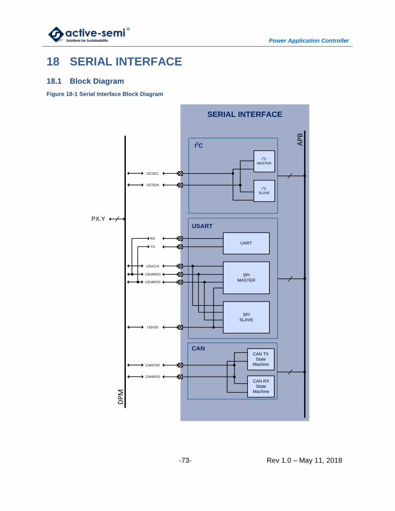
Power Application Controller
-73- Rev 1.0 – May 11, 2018
18 SERIAL INTERFACE
18.1 Block Diagram
Figure 18-1 Serial Interface Block Diagram
I2C A
PB
I2CSCL
SERIAL INTERFACE
I2C
MASTER
I2C
SLAVE
I2CSDA
SPIUSxCLK
SPI
MASTER
USxMISO
SPI
SLAVE
USxMOSI
USxSS
CANCAN TX
State
Machine
CAN RX
State
Machine
CANTXD
CANRXD
UARTRX
TX
USART
DP
M
PX.Y
Power Application Controller
-74- Rev 1.0 – May 11, 2018
18.2 Functional Description
The PAC55XX has three types of serial interfaces: I2C, USART and CAN. The PAC55XX has
one I2C controller, one CAN controller and up to 3 USARTs.
18.3 I2C Controller
The PAC55XX contains one I2C controller. This is a configurable APB peripheral and the clock
input is PCLK. This peripheral has an input clock divider that can be used to generate various
master clock frequencies. The I2C controller can support various modes of operation:
I2C master operation
o Standard (100kHz), full-speed (400kHz), fast (1MHz) or high-speed modes (3.4MHz)
o Single and multi-master
o Synchronization (multi-master)
o Arbitration (multi-master)
o 7-bit or 10-bit slave addressing
I2C slave operation
o Standard (100kHz), full-speed (400kHz), fast (1MHz) or high-speed modes (3.4MHz)
o Clock stretching
o 7-bit or 10-bit slave addressing
The I2C peripheral may operate either by polling, or can be configured to be interrupt driven for
both receive and transmit operations.
18.4 USART
The PAC55XX contains up to 2 Universal Synchronous Receive Transmit (USART) peripherals.
Each USART is a configurable APB bus client and input clock is PCLK. These peripherals have
a configurable clock divider that can be used to produce various frequencies for the UART or
SPI master peripheral.
The number of these peripherals depends on the peripheral MUX configuration. See the IO
Controller section on information on how to configure the peripheral MUX with the USART
peripheral.
The USART peripheral supports two main modes: SPI mode and UART mode.
18.4.1 USART SPI Mode
Master or slave mode operation
8-bit, 16-bit or 32-bit word transfers
Configurable clock polarity (active high or active low)
Configurable data phase (setup/sample or sample/setup)
Power Application Controller
-75- Rev 1.0 – May 11, 2018
Interrupts and status flags for RX and TX operations
Support for up to 25MHz SPI clock
18.4.2 USART UART Mode
8-bit data
Programmable data bit rate
Maximum baud rate of 1Mbaud
RX and TX FIFOs
Configurable stop bits (1 or 2)
Configurable parity: even, odd, none
o Mark/space support for 9-bit addressing protocols
Interrupt and status flags for RX and TX operations
18.5 CAN
The PAC55XX contains one Controller Area Network (CAN) peripheral. The CAN peripheral is a
configurable APB bus client and input clock is PCLK. This peripheral has a configurable clock
divider that can be used to produce various frequencies for the CAN peripheral.
CAN 2.0B support
1Mb/s data rate
64-byte receive FIFO
16-byte transmit buffer
Standard and extended frame support
Arbitration
Overload frame generated on FIFO overflow
Normal and Listen Only modes supported
Interrupt and status flags for RX and TX operations
Power Application Controller
-76- Rev 1.0 – May 11, 2018
18.6 Dynamic Characteristics
Table 18-1 Serial Interface Dynamic Characteristics
(VCCIO = 3.3V, VSYS = 5V, VCORE = 1.2V, and TA = -40C to 125C unless otherwise specified.)
SYMBOL PARAMETER CONDITIONS MIN TYP MAX UNIT
I2C
fI2CCLK I2C input clock frequency
Standard mode (100kHz) 2.8 MHz
Full-speed mode (400kHz) 2.8 MHz
Fast mode (1MHz) 6.14 MHz
High-speed mode (3.4MHz) 20.88 MHz
USART (UART mode)
fUARTCLK USART input clock frequency fPCLK/16 MHz
fUARTBAUD UART baud rate fUSARTCLK = 7.1825MHz 1 Mbps
USART (SPI mode)
fSPICLK USART input clock frequency Master mode 50 MHz
Slave mode 50 MHz
fUSARTSPICLK USART SPI clock frequency Master mode 25 MHz
Slave mode 25 MHz
CAN
fCANCLK CAN input clock frequency 50 MHz
fCANTX CAN transmit clock frequency 1 Mbps
fCANRX CAN receive clock frequency 1 Mbps
Table 18-2 I2C Dynamic Characteristics
(VCCIO = 3.3V, VSYS = 5V, VCORE = 1.2V, and TA = -40C to 125C unless otherwise specified.)
SYMBOL PARAMETER CONDITIONS MIN TYP MAX UNIT
fSCL SCL clock frequency
Standard mode 0 100 kHz
Full-speed mode 0 400 kHz
Fast mode 0 1 MHz
tLOW SCL clock low
Standard mode 4.7 µs
Full-speed mode 1.3 µs
Fast mode 0.5 µs
tHIGH SCL clock high
Standard mode 4.0 µs
Full-speed mode 0.6 µs
Fast mode 0.26 µs
Power Application Controller
-77- Rev 1.0 – May 11, 2018
tHD;STA Hold time for a repeated START condition
Standard mode 4.0 µs
Full-speed mode 0.6 µs
Fast mode 0.26 µs
tSU;STA Set-up time for a repeated START condition
Standard mode 4.7 µs
Full-speed mode 0.6 µs
Fast mode 0.26 µs
tHD;DAT Data hold time
Standard mode 0 3.45 µs
Full-speed mode 0 0.9 µs
Fast mode 0 µs
tSU;DAT Data setup time
Standard mode 250 ns
Full-speed mode 100 ns
Fast mode 50 ns
tSU;STO Set-up time for STOP condition
Standard mode 4.0 µs
Full-speed mode 0.6 µs
Fast mode 0.26 µs
tBUF Bus free time between a STOP and START condition
Standard mode 4.7 µs
Full-speed mode 1.3 µs
Fast mode 0.5 µs
tr Rise time for SDA and SCL
Standard mode 1000 ns
Full-speed mode 20 300 ns
Fast mode 120 ns
tf Fall time for SDA and SCL
Standard mode 300 ns
Full-speed mode 300 ns
Fast mode 120 ns
Cb Capacitive load for each bus line
Standard mode, full-speed mode
400 pF
Fast mode 550 pF
Figure 18-2 I2C Timing Diagram
Power Application Controller
-78- Rev 1.0 – May 11, 2018
Power Application Controller
-79- Rev 1.0 – May 11, 2018
19 PWM TIMERS
19.1 Block Diagram
Figure 19-1 PWM Timers Block Diagram
AP
B
PWM TIMERS
SYN
C
TIMER A PWM/CCR
TAPWM[3:0]
DEAD TIME
GENERATOR
CAPTURE &
COMPARE
CAPTURE &
COMPARE
TIMER A
16-BIT
QEP
ENCODER
TAIDX
TAPHA
TAPHB
TAPWM[7:4]
TIMER A PWM/CCR
TAPWM[3:0]
DEAD TIME
GENERATOR
CAPTURE &
COMPARE
CAPTURE &
COMPARE
TIMER A
16-BIT
QEP
ENCODER
TAIDX
TAPHA
TAPHB
TAPWM[7:4]
TIMER B PWM/CCR
TBPWM[3:0]
DEAD TIME
GENERATOR
CAPTURE &
COMPARE
CAPTURE &
COMPARE
TIMER B
16-BIT
QEP
ENCODER
TBIDX
TBPHA
TBPHB
TBPWM[7:4]
TIMER B PWM/CCR
TBPWM[3:0]
DEAD TIME
GENERATOR
CAPTURE &
COMPARE
CAPTURE &
COMPARE
TIMER B
16-BIT
QEP
ENCODER
TBIDX
TBPHA
TBPHB
TBPWM[7:4]
TIMER C PWM/CCR
TCPWM[3:0]
DEAD TIME
GENERATOR
CAPTURE &
COMPARE
CAPTURE &
COMPARE
TIMER C
16-BIT
QEP
ENCODER
TCIDX
TCPHA
TCPHB
TCPWM[7:4]
TIMER C PWM/CCR
TCPWM[3:0]
DEAD TIME
GENERATOR
CAPTURE &
COMPARE
CAPTURE &
COMPARE
TIMER C
16-BIT
QEP
ENCODER
TCIDX
TCPHA
TCPHB
TCPWM[7:4]
TIMER D PWM/CCR
TDPWM[3:0]
DEAD TIME
GENERATOR
CAPTURE &
COMPARE
CAPTURE &
COMPARE
TIMER D
16-BIT
QEP
ENCODER
TDIDX
TDPHA
TDPHB
TDPWM[7:4]
TIMER D PWM/CCR
TDPWM[3:0]
DEAD TIME
GENERATOR
CAPTURE &
COMPARE
CAPTURE &
COMPARE
TIMER D
16-BIT
QEP
ENCODER
TDIDX
TDPHA
TDPHB
TDPWM[7:4]
DP
M
PX.Y
Power Application Controller
-80- Rev 1.0 – May 11, 2018
19.2 Timer Features
Configurable input clock source: PCLK or ACLK
Up to 300MHz input clock
3-bit Input clock divider
Timer counting modes
o up, up/down and asymmetric
Timer latch modes
o Latch when counter = 0
o Latch when counter = period
o Latch when CCR value written
o Latch all CCR values at same time
Base timer interrupts
Single shot or auto-reload
19.2.1 CCR/PWM Timer
PWM output or capture input
CCR interrupt enable
CCR interrupt skips
SW force CCR interrupt
CCR interrupt type
o Rising, falling or both
CCR compare latch modes
o Latch when counter = 0
o Latch when counter = period
o Latch immediate
CCR capture latch modes
o Latch on rising edge
o Latch on falling edge
o Latch on both rising and falling edges
Invert CCR output
CCR phase delay for phase shifted drive topologies
ADC trigger outputs
o PWM rising edge or falling edge
19.2.2 Dead-time Generators (DTG)
DTG enabled
12-bit rising edge delay
Power Application Controller
-81- Rev 1.0 – May 11, 2018
12-bit falling edge delay
19.2.3 QEP Decoder
QEP encoder enabled
Direction status
Configurable Interrupts:
o Phase A rising edge
o Phase B rising edge
o Index event
o Counter wrap
4 different counting modes for best resolution, range and speed performance
Power Application Controller
-82- Rev 1.0 – May 11, 2018
20 GENERAL PURPOSE TIMERS
20.1 Block Diagram
Figure 20-1 SOC Bus Watchdog and Wake-up Timer
SOC
SOC BUS
WATCHDOG
WAKE-UP
TIMERSOC BUS
AH
B/A
PB
SOC BUS WATCHDOG AND WAKE-UP TIMER
SOC
SOC BUS
WATCHDOG
WAKE-UP
TIMERSOC BUS
AH
B/A
PB
SOC BUS WATCHDOG AND WAKE-UP TIMER
Figure 20-2 General Purpose Timers
AH
B
GENERAL PURPOSE TIMERS
24-bit
Timer
Calendar/
Alarm
RTC
24-bit
Timer
POR
Logic
WWDT
RESET
24-bit
Timer
GP Timers
AP
B
AH
B
GENERAL PURPOSE TIMERS
24-bit
Timer
Calendar/
Alarm
RTC
24-bit
Timer
POR
Logic
WWDT
RESET
24-bit
Timer
GP Timers
AP
B
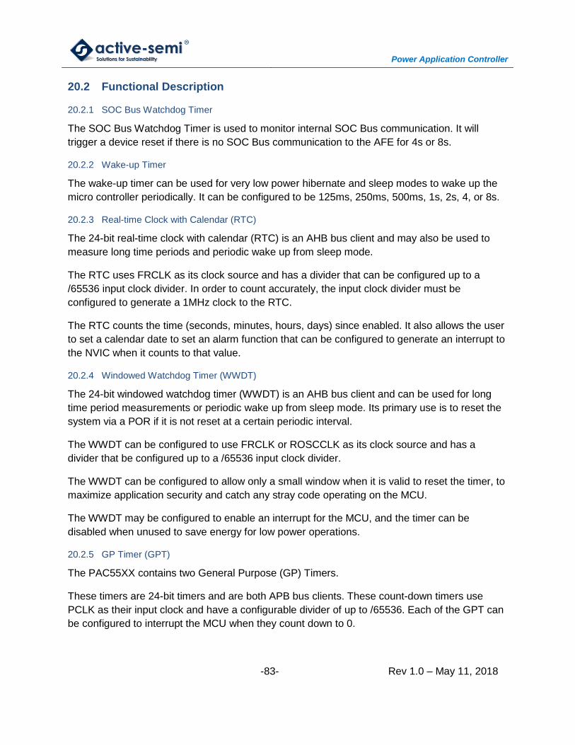
Power Application Controller
-83- Rev 1.0 – May 11, 2018
20.2 Functional Description
20.2.1 SOC Bus Watchdog Timer
The SOC Bus Watchdog Timer is used to monitor internal SOC Bus communication. It will
trigger a device reset if there is no SOC Bus communication to the AFE for 4s or 8s.
20.2.2 Wake-up Timer
The wake-up timer can be used for very low power hibernate and sleep modes to wake up the
micro controller periodically. It can be configured to be 125ms, 250ms, 500ms, 1s, 2s, 4, or 8s.
20.2.3 Real-time Clock with Calendar (RTC)
The 24-bit real-time clock with calendar (RTC) is an AHB bus client and may also be used to
measure long time periods and periodic wake up from sleep mode.
The RTC uses FRCLK as its clock source and has a divider that can be configured up to a
/65536 input clock divider. In order to count accurately, the input clock divider must be
configured to generate a 1MHz clock to the RTC.
The RTC counts the time (seconds, minutes, hours, days) since enabled. It also allows the user
to set a calendar date to set an alarm function that can be configured to generate an interrupt to
the NVIC when it counts to that value.
20.2.4 Windowed Watchdog Timer (WWDT)
The 24-bit windowed watchdog timer (WWDT) is an AHB bus client and can be used for long
time period measurements or periodic wake up from sleep mode. Its primary use is to reset the
system via a POR if it is not reset at a certain periodic interval.
The WWDT can be configured to use FRCLK or ROSCCLK as its clock source and has a
divider that be configured up to a /65536 input clock divider.
The WWDT can be configured to allow only a small window when it is valid to reset the timer, to
maximize application security and catch any stray code operating on the MCU.
The WWDT may be configured to enable an interrupt for the MCU, and the timer can be
disabled when unused to save energy for low power operations.
20.2.5 GP Timer (GPT)
The PAC55XX contains two General Purpose (GP) Timers.
These timers are 24-bit timers and are both APB bus clients. These count-down timers use
PCLK as their input clock and have a configurable divider of up to /65536. Each of the GPT can
be configured to interrupt the MCU when they count down to 0.
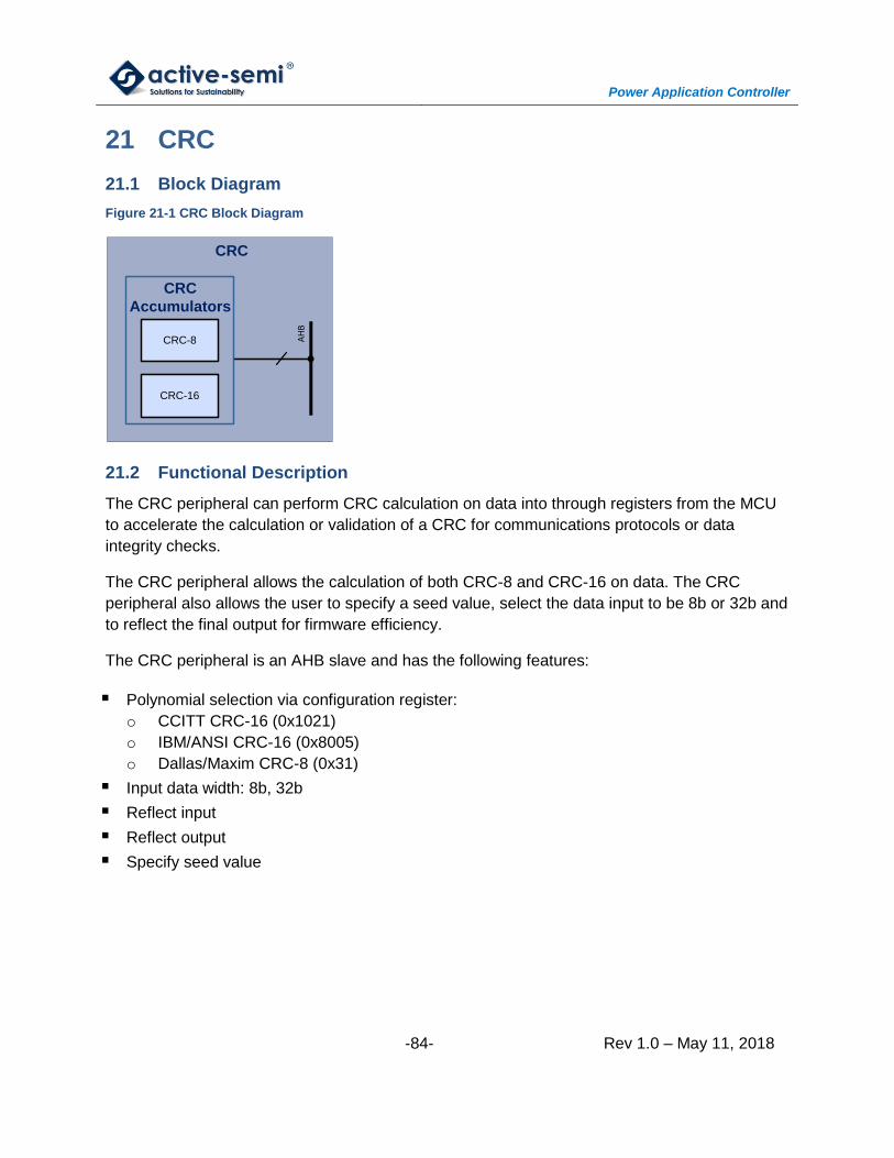
Power Application Controller
-84- Rev 1.0 – May 11, 2018
21 CRC
21.1 Block Diagram
Figure 21-1 CRC Block Diagram
CRC
Accumulators
CRC-16
CRC-8 AH
B
CRC
21.2 Functional Description
The CRC peripheral can perform CRC calculation on data into through registers from the MCU
to accelerate the calculation or validation of a CRC for communications protocols or data
integrity checks.
The CRC peripheral allows the calculation of both CRC-8 and CRC-16 on data. The CRC
peripheral also allows the user to specify a seed value, select the data input to be 8b or 32b and
to reflect the final output for firmware efficiency.
The CRC peripheral is an AHB slave and has the following features:
Polynomial selection via configuration register:
o CCITT CRC-16 (0x1021)
o IBM/ANSI CRC-16 (0x8005)
o Dallas/Maxim CRC-8 (0x31)
Input data width: 8b, 32b
Reflect input
Reflect output
Specify seed value
Power Application Controller
-85- Rev 1.0 – May 11, 2018
22 THERMAL CHARACTERISTICS
Table 22-1 Thermal Characteristics
PARAMETER VALUE UNIT
Operating ambient temperature range -40 to 125 C
Operating junction temperature range -40 to 150 C
Storage temperature range -55 to 150 C
Lead temperature (Soldering, 10 seconds) 300 C
Junction-to-case thermal resistance (JC) 2.897 C/W
Junction-to-ambient thermal resistance (JA) 23.36 C/W
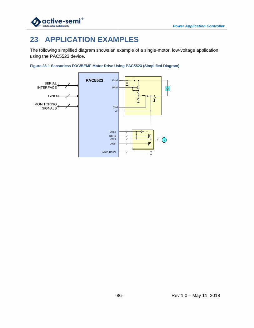
Power Application Controller
-86- Rev 1.0 – May 11, 2018
23 APPLICATION EXAMPLES
The following simplified diagram shows an example of a single-motor, low-voltage application
using the PAC5523 device.
Figure 23-1 Sensorless FOC/BEMF Motor Drive Using PAC5523 (Simplified Diagram)
MM
SERIAL
INTERFACE
GPIO
MONITORING
SIGNALS
PAC5523
DRBx
DRHxDRSx
DRLx
V
DAxP, DAxN
VP
DRM
CSM
VHM
+++
+++
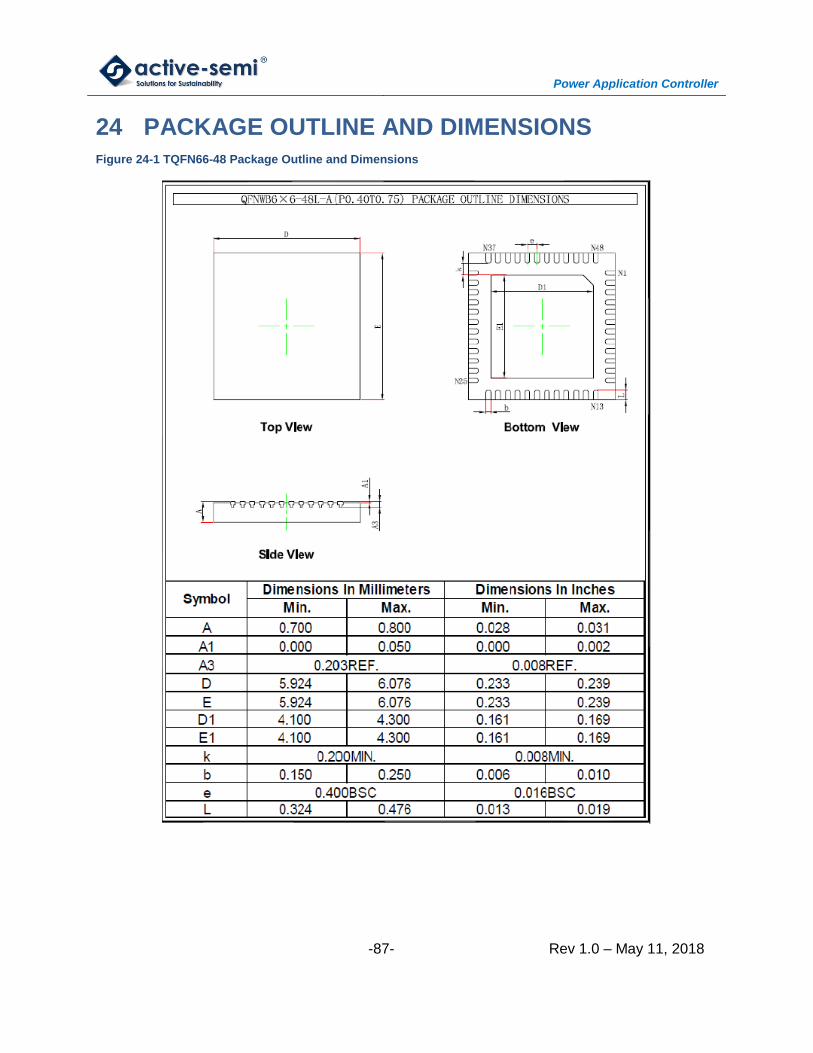
Power Application Controller
-87- Rev 1.0 – May 11, 2018
24 PACKAGE OUTLINE AND DIMENSIONS
Figure 24-1 TQFN66-48 Package Outline and Dimensions
Power Application Controller
-88- Rev 1.0 – May 11, 2018
25 LEGAL INFORMATION
Copyright © 2018 Active-Semi, Inc. All rights reserved.
All information provided in this document is subject to legal disclaimers.
Active-Semi reserves the right to modify its products, circuitry or product specifications without notice. Active-Semi
products are not intended, designed, warranted or authorized for use as critical components in life-support, life-critical
or safety-critical devices, systems, or equipment, nor in applications where failure or malfunction of any Active-Semi
product can reasonably be expected to result in personal injury, death or severe property or environmental damage.
Active-Semi accepts no liability for inclusion and/or use of its products in such equipment or applications. Active-Semi
does not assume any liability arising out of the use of any product, circuit, or any information described in this
document. No license, express, implied or otherwise, is granted under any patents, copyrights or other intellectual
property rights of Active-Semi or others. Active-Semi assumes no liability for any infringement of the intellectual
property rights or other rights of third parties which would result from the use of information contained herein.
Customers should evaluate each product to make sure that it is suitable for their applications. Customers are
responsible for the design, testing, and operation of their applications and products using Active-Semi products.
Customers should provide appropriate design and operating safeguards to minimize the risks associated with their
applications and products. All products are sold subject to Active-Semi's terms and conditions of sale supplied at the
time of order acknowledgment. Exportation of any Active-Semi product may be subject to export control laws.
Power Application Controller®
is a registered trademark of Active-Semi, Inc. Active-SemiTM
, Active-Semi logo,
Solutions for SustainabilityTM
, Micro Application ControllerTM
, Multi-Mode Power ManagerTM
, Configurable Analog
Front EndTM
, and Application Specific Power DriversTM
are trademarks of Active-Semi, Inc.
ARM©
and Cortex® are registered trademarks of ARM Limited. All referenced brands and trademarks are the property
of their respective owners.
For more information on this and other products, contact [email protected] or visit www.active-semi.com.