Embed Size (px)
Citation preview
PRELIMINARY
EVB71122 300 to 930MHz Receiver
Evaluation Board Description
39012 71122 01 Page 1 of 32 EVB Description Rev. 002 April/08
Features
Programmable PLL synthesizer 8-channel preconfigured or fully programmable SPI mode Double super-heterodyne receiver architecture with 2nd mixer as image rejection mixer Reception of FSK, FM and ASK modulated signals Low shut-down and operating currents AGC – automatic gain control On-chip IF filter Fully integrated FSK/FM demodulator RSSI for level indication and ASK detection 2nd order low-pass data filter Positive and negative peak detectors Data slicer (with averaging or peak-detector adaptive threshold) 32-pin Quad Flat No-Lead Package (QFN) EVB programming software is available on Melexis web site
Ordering Information Part No. (see paragraph 6) EVB71122-315-C EVB71122-868-C
71122-915-C
.3 or 915MHz).
ples
EVB71122-433-C EVB *SPI mode is default population, ABC mode according to paragraph 5 **EVB71122-XXX-C with XXX = Reception frequency (315 or 433.92 or 868***The evaluation board is supplied with a SMA connector.
Application Exam
General digitaat 300 to 930M
l and analog RF receivers Hz
ss en ) Tire pressure monitoring systems (TPMS) Remote keyle try (RKE Low power telemetry systems Alarm and security systems Active RFID tags Remote controls Garage door openers Home and building automation
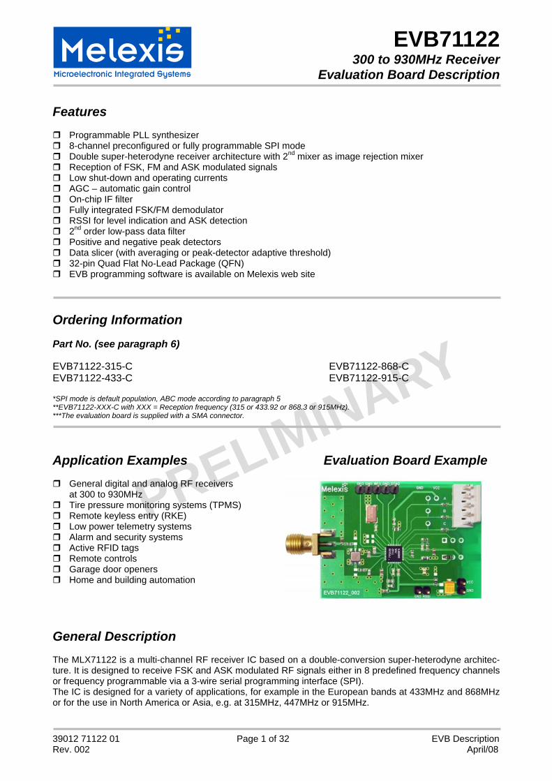
Evaluation Board Example
General Description The MLX71122 is a multi-channel RF receiver IC based on a double-conversion super-heterodyne architec-ture. It is designed to receive FSK and ASK modulated RF signals either in 8 predefined frequency channels or frequency programmable via a 3-wire serial programming interface (SPI). The IC is designed for a variety of applications, for example in the European bands at 433MHz and 868MHz or for the use in North America or Asia, e.g. at 315MHz, 447MHz or 915MHz.
PRELIMINARY
EVB71122 300 to 930MHz Receiver
Evaluation Board Description
39012 71122 01 Page 2 of 32 EVB Description Rev. 002 April/08
Document Content
1 Theory of Operation...................................................................................................4 1.1 General ............................................................................................................................. 4 1.2 EVB Data Overview.......................................................................................................... 4 1.3 Block Diagram .................................................................................................................. 5 1.4 Enable/Disable in ABC Mode ........................................................................................... 6 1.5 Demodulation Selection in ABC Mode.............................................................................. 6 1.6 Programming Modes ........................................................................................................ 6 1.7 Preconfigured Frequencies in ABC Mode ........................................................................ 6
2 Functional Description ..............................................................................................7 2.1 Frequency Planning.......................................................................................................... 7 2.2 Calculation of Counter Settings ........................................................................................ 8
2.2.1 Calculation of LO1 and IF1 frequency for Low Frequency Bands............................................... 8 2.2.2 Calculation of LO1 and IF1 frequency for High Frequency Bands.............................................. 9 2.2.3 Counter Setting Examples for SPI Mode..................................................................................... 9 2.2.4 Counter Settings in ABC Mode – 8+1 Preconfigured Channels................................................ 10 2.2.5 PLL Counter Ranges ................................................................................................................. 11
2.3 SPI Description............................................................................................................... 11 2.3.1 General ...................................................................................................................................... 11 2.3.2 Read / Write Sequences............................................................................................................ 12 2.3.3 Serial Programming Interface Timing ........................................................................................ 12
3 Register Description ................................................................................................13 3.1 Register Overview .......................................................................................................... 13
3.1.1 Control Word R0 ........................................................................................................................ 15 3.1.2 Control Word R1 ........................................................................................................................ 16 3.1.3 Control Word R2 ........................................................................................................................ 17 3.1.4 Control Word R3 ........................................................................................................................ 17 3.1.5 Control Word R4 ........................................................................................................................ 18 3.1.6 Control Word R5 ........................................................................................................................ 18 3.1.7 Control Word R6 ........................................................................................................................ 18 3.1.8 Control Word R7 (Read-only Register)...................................................................................... 19
4 Application Circuits for SPI Mode...........................................................................20 4.1 Averaging Data Slicer Configured for Bi-Phase Codes .................................................. 20 4.2 Peak Detector Data Slicer Configured for NRZ Codes................................................... 22
4.2.1 Board Component Values List (SPI mode)................................................................................ 24
5 Application for 8-Channel Preconfigured (ABC) Mode .........................................25 5.1 Averaging Data Slicer Configured for Bi-Phase Codes .................................................. 25
5.1.1 Board Component Values List (ABC mode) .............................................................................. 27
PRELIMINARY
EVB71122 300 to 930MHz Receiver
Evaluation Board Description
39012 71122 01 Page 3 of 32 EVB Description Rev. 002 April/08
6 Evaluation Board Layouts .......................................................................................28
7 Package Description................................................................................................29 7.1 Soldering Information ..................................................................................................... 29
8 Reliability Information .............................................................................................30
9 ESD Precautions ......................................................................................................30
10 Disclaimer .................................................................................................................32
PRELIMINARY
EVB71122 300 to 930MHz Receiver
Evaluation Board Description
39012 71122 01 Page 4 of 32 EVB Description Rev. 002 April/08
1 Theory of Operation 1.1 General The MLX71122 receiver architecture is based on a double-conversion super-heterodyne approach. The two LO signals are derived from an on-chip integer-N PLL frequency synthesizer. The PLL reference frequency is derived from a crystal (XTAL). The PLL synthesizer consists of an integrated voltage-controlled oscillator with external inductor, a programmable feedback divider chain, a programmable reference divider, a phase-frequency detector with a charge pump and an external loop filter. In the receiver’s down-conversion chain, two mixers MIX1 and MIX2 are driven by the internal local oscillator signals LO1 and LO2, respectively. The second mixer MIX2 is an image-reject mixer. As the first intermedi-ate frequency (IF1) is very high (typically above 100 MHz), a reasonably high degree of image rejection is provided even without using an RF front-end filter. At applications asking for very high image rejections, cost-efficient RF front-end filtering can be realized by using a SAW filter in front of the LNA. The receiver signal chain is set up by a low noise amplifier (LNA), two down-conversion mixers (MIX1 and MIX2), an on-chip IF filter (IFF) as well as an IF amplifier (IFA). By choosing the required modulation via an FSK/ASK switch (at pin MODSEL), either the on-chip FSK demodulator (FSK DEMOD) or the RSSI-based ASK detector is selected. A second order data filter (OA1) and a data slicer (OA2) follow the demodulator. The data slicer threshold can be generated from the mean-value of the data stream or by means of the posi-tive and negative peak detectors (PKDET+/-). In general the MLX71122 can be set to shut-down mode, where all receiver functions are completely turned off, and to several other operating modes. There are two global operating modes that are selectable via the logic level at pin SPISEL:
• 8-channel preconfigured mode (ABC mode) • fully programmable mode (SPI mode).
In ABC mode the number of frequency channels is limited to eight but no microcontroller programming is required. In this case the three lines of the serial programming interface (SPI) are used to select one of the eight predefined frequency channels via simple 3-bit parallel programming. Pins ENRX and MODSEL are used to enable/disable the receiver and to select FSK or ASK demodulation, respectively. SPI mode is recommended for full programming flexibility. In this case the three lines of the SPI are config-ured as a standard 3-wire bus (SDEN, SDTA and SCLK). This allows changing many parameters of the receiver, for example more operating modes, channels, frequency resolutions, gains, demodulation types, data slicer settings and more. The pin MODSEL has no effect in this mode.
1.2 EVB Data Overview Input frequency ranges: 300 to 930MHz Power supply range: 3.0 to 5.5V Temperature range: -40 to +105°C Shutdown current: 50nA Operating current: 12mA (typ.) Internal IF2: 2MHz with 230kHz 3dB bandwidth Maximum data rate: 100kbps NRZ code,
50kbps bi-phase code Minimum frequency resolution: 10kHz
Total image rejection: > 65dB (with external RF front-end filter)
FSK/FM deviation range: ±2 to ±50kHz Spurious emission: < -70dBm Linear RSSI range: > 50dB FSK input frequency acceptance range:
180kHz (3dB) Crystal reference frequency: 10MHz
Input Sensitivity: at 4 kbps NRZ, BER = 3·10-3 Frequency 315 MHZ 433 MHz 868 MHz 915 MHz
FSK: ±20 kHz deviation -106dBm -104dBm -101dBm -101dBm ASK -108dBm -108dBm -106dBm -106dBm
PRELIMINARY
EVB71122 300 to 930MHz Receiver
Evaluation Board Description
39012 71122 01 Page 5 of 32 EVB Description Rev. 002 April/08
1.3 Block Diagram
FSKDEMOD
ControlLogic
MODS
EL
SLCSEL
BIAS
ENRX
RBIA
S
VEEA
NA
VCCD
IG
VEED
IG
OA2
DFOOA1
PKDET+
PKDET_
SLC
PDP
PDN
DTAO
DF2
DF1 29
27
26
30
25
32
28
22
2016 21SPIS
EL
A/SC
LK
B/SD
TA
C/SD
EN
17 18 197 10
200k 200k
SW2
SW1
200k
1M1M
ASK
FSK
LNAO
LNA
VEEL
NA
VCCA
NA
LNAI
43
31
21
VCCV
CO
VEEV
CO
1411 MFO
23
Rcounter
N / Acounter PFD
VCO
LF CP RO
LO2DIV
VEEI
F 9MI
XN
MIXP
RSSI
IFA
LO2
IF2IF1
LO1
MIX1 MIX2 IFF
5 6 8
LF15 ROI
24TNK1 TNK212 13
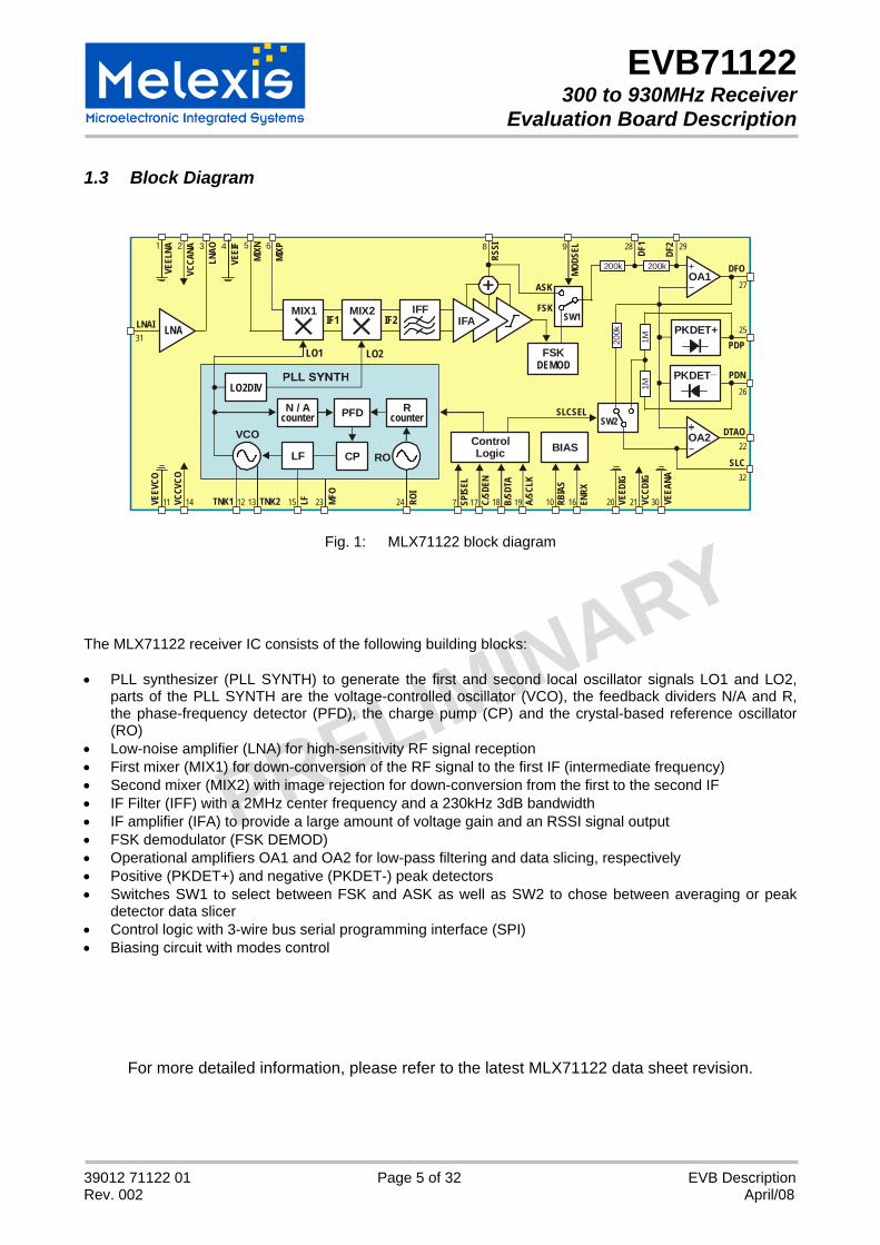
Fig. 1: MLX71122 block diagram
The MLX71122 receiver IC consists of the following building blocks: • PLL synthesizer (PLL SYNTH) to generate the first and second local oscillator signals LO1 and LO2,
parts of the PLL SYNTH are the voltage-controlled oscillator (VCO), the feedback dividers N/A and R, the phase-frequency detector (PFD), the charge pump (CP) and the crystal-based reference oscillator (RO)
• Low-noise amplifier (LNA) for high-sensitivity RF signal reception • First mixer (MIX1) for down-conversion of the RF signal to the first IF (intermediate frequency) • Second mixer (MIX2) with image rejection for down-conversion from the first to the second IF • IF Filter (IFF) with a 2MHz center frequency and a 230kHz 3dB bandwidth • IF amplifier (IFA) to provide a large amount of voltage gain and an RSSI signal output • FSK demodulator (FSK DEMOD) • Operational amplifiers OA1 and OA2 for low-pass filtering and data slicing, respectively • Positive (PKDET+) and negative (PKDET-) peak detectors • Switches SW1 to select between FSK and ASK as well as SW2 to chose between averaging or peak
detector data slicer • Control logic with 3-wire bus serial programming interface (SPI) • Biasing circuit with modes control
For more detailed information, please refer to the latest MLX71122 data sheet revision.
P ELAR
RIMIN
Y
EVB71122 300 to 930MHz Receiver
Evaluation Board Description
39012 71122 01 Page 6 of 32 EVB Description Rev. 002 April/08
1.4 Enable/Disable in ABC Mode
ENRX Description 0 Shutdown mode 1 Receive mode
Pin ENRX is pulled down internally. Device is in shutdown by default, after power supply on. If ENRX = 0 and SPISEL = 1 then operating modes according to OPMODE bit (refer to control word R0). If ENRX = 1 then OPMODE bit has no effect (hardwired receive mode).
1.5 Demodulation Selection in ABC Mode
MODSEL Description 0 FSK demodulation 1 ASK demodulation
Pin MODSEL has no effect in SPI mode (SPISEL = 1). We recommend connecting it to ground to avoid a floating CMOS gate.
1.6 Programming Modes
SPISEL Description 0 ABC mode (8 channels preconfigured) 1 SPI mode (programming via 3-wire bus)
1.7 Preconfigured Frequencies in ABC Mode
A B C Receive Frequency 0 0 0 FSK1: 369.5 MHz 0 1 0 FSK5: 388.3 MHz 1 0 0 FSK2: 371.1 MHz 1 1 0 FSK4: 376.9 MHz 0 0 1 FSK3: 375.3 MHz 0 1 1 FSK7: 394.3 MHz 1 0 1 FSK6: 391.5 MHz 1 1 1 FSK8: 395.9 MHz
As all pins, pins A, B, and C are equipped with ESD protection diodes that are tied to VCC and to VEE. Therefore these pins should not be directly connected to positive supply (a logic “1”) before the supply volt-age is applied to the IC. Otherwise the IC will be supplied through these control lines and it may enter into an unpredictable mode. In case the user wants to apply a positive supply voltage to these pins before the sup-ply voltage is applied to the IC, a protection resistor should be inserted in each control line.
PRELIMINARY
EVB71122 300 to 930MHz Receiver
Evaluation Board Description
39012 71122 01 Page 7 of 32 EVB Description Rev. 002 April/08
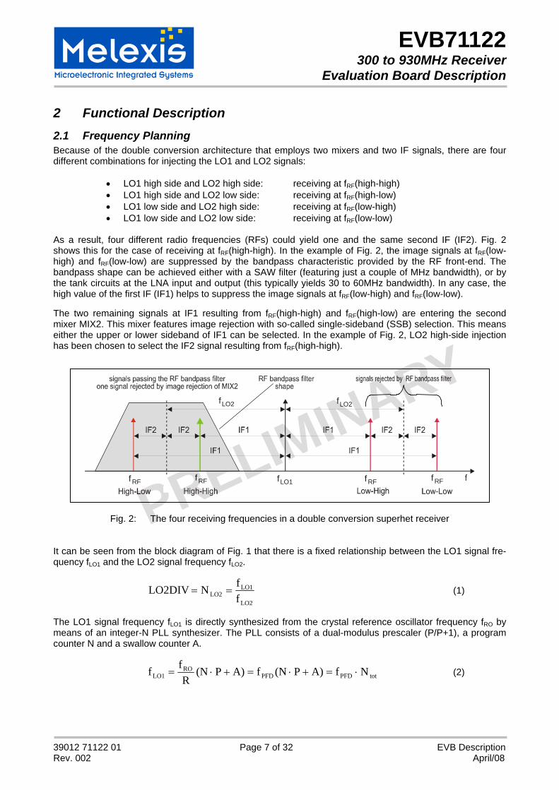
2 Functional Description 2.1 Frequency Planning Because of the double conversion architecture that employs two mixers and two IF signals, there are four different combinations for injecting the LO1 and LO2 signals:
• LO1 high side and LO2 high side: receiving at fRF(high-high) • LO1 high side and LO2 low side: receiving at fRF(high-low) • LO1 low side and LO2 high side: receiving at fRF(low-high) • LO1 low side and LO2 low side: receiving at fRF(low-low)
As a result, four different radio frequencies (RFs) could yield one and the same second IF (IF2). Fig. 2 shows this for the case of receiving at fRF(high-high). In the example of Fig. 2, the image signals at fRF(low-high) and fRF(low-low) are suppressed by the bandpass characteristic provided by the RF front-end. The bandpass shape can be achieved either with a SAW filter (featuring just a couple of MHz bandwidth), or by the tank circuits at the LNA input and output (this typically yields 30 to 60MHz bandwidth). In any case, the high value of the first IF (IF1) helps to suppress the image signals at fRF(low-high) and fRF(low-low). The two remaining signals at IF1 resulting from fRF(high-high) and fRF(high-low) are entering the second mixer MIX2. This mixer features image rejection with so-called single-sideband (SSB) selection. This means either the upper or lower sideband of IF1 can be selected. In the example of Fig. 2, LO2 high-side injection has been chosen to select the IF2 signal resulting from fRF(high-high).
fLO2 fLO2
fLO1 fRFfRFfRFfRF
Fig. 2: The four receiving frequencies in a double conversion superhet receiver
It can be seen from the block diagram of Fig. 1 that there is a fixed relationship between the LO1 signal fre-quency fLO1 and the LO2 signal frequency fLO2.
LO2
LO1LO2 f
fN LO2DIV == (1)
The LO1 signal frequency fLO1 is directly synthesized from the crystal reference oscillator frequency fRO by means of an integer-N PLL synthesizer. The PLL consists of a dual-modulus prescaler (P/P+1), a program counter N and a swallow counter A.
totPFDPFDRO
LO1 NfA)P(NfA)P(NR
ff ⋅=+⋅=+⋅= (2)
PRE IMR
LINA Y
EVB71122 300 to 930MHz Receiver
Evaluation Board Description
39012 71122 01 Page 8 of 32 EVB Description Rev. 002 April/08
Due to the double superhet receiver architecture, the channel frequency step size fCH is not equal to the phase-frequency detector (PFD) frequency fPFD. For high-side injection, the channel step size fCH is given by:
LO2
LO2PFD
LO2
LO2ROCH N
1NfN
1NR
ff −=
−= (3)
While the following equation is valid for low-side injection:
LO2
LO2PFD
LO2
LO2ROCH N
1NfN
1NR
ff +=
+= (4)
2.2 Calculation of Counter Settings Frequency planning and the selection of the MLX71122’s PLL counter settings are straightforward and can be laid out on the following procedure. Usually the receive frequency fRF and the channel step size fCH are given by system requirements. The N and A counter settings can be derived from Ntot or fLO1 and fPFD by using the following equations.
)32
Nfloor()P
Nfloor(N tottot == ; 32NNPNNA tottot ⋅−=⋅−= (5)
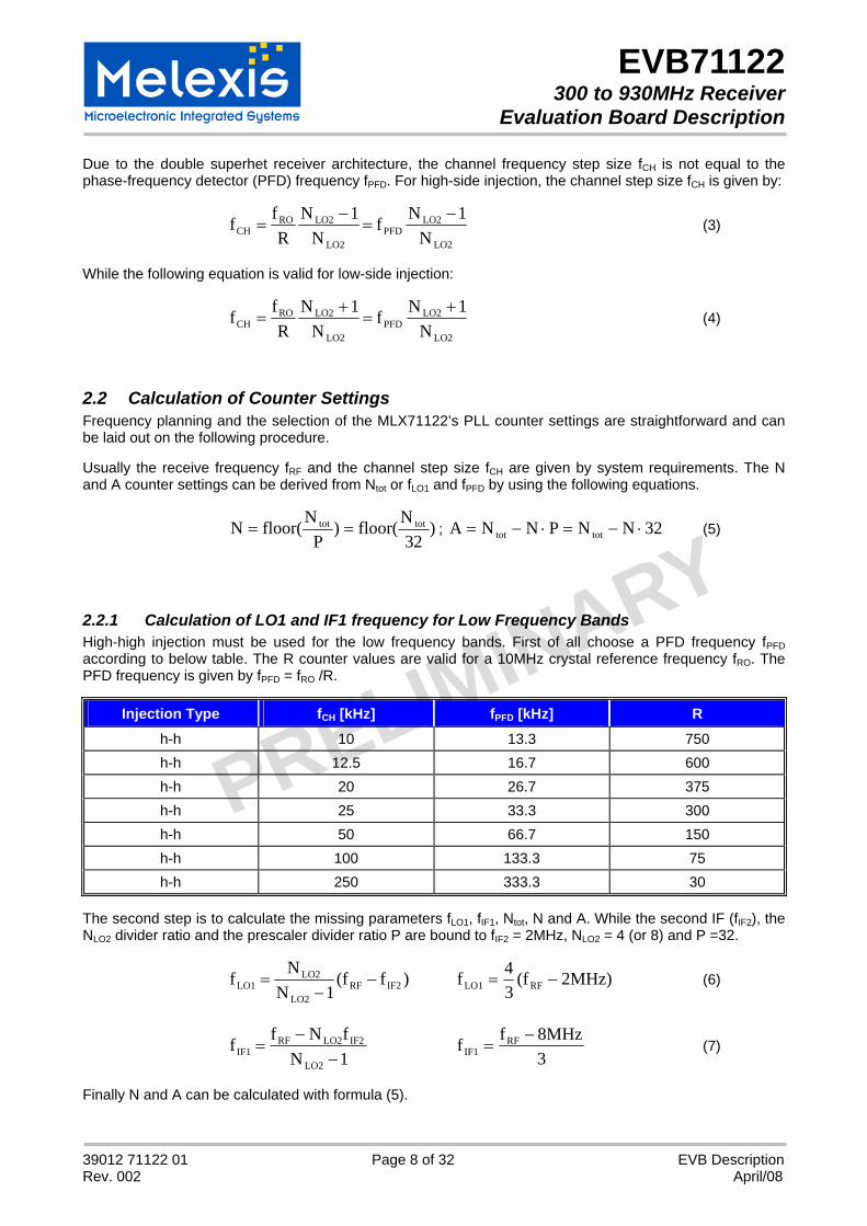
2.2.1 Calculation of LO1 and IF1 frequency for Low Frequency Bands High-high injection must be used for the low frequency bands. First of all choose a PFD frequency fPFD according to below table. The R counter values are valid for a 10MHz crystal reference frequency fRO. The PFD frequency is given by fPFD = fRO /R.
Injection Type fCH [kHz] fPFD [kHz] R h-h 10 13.3 750 h-h 12.5 16.7 600 h-h 20 26.7 375 h-h 25 33.3 300 h-h 50 66.7 150 h-h 100 133.3 75 h-h 250 333.3 30
The second step is to calculate the missing parameters fLO1, fIF1, Ntot, N and A. While the second IF (fIF2), the NLO2 divider ratio and the prescaler divider ratio P are bound to fIF2 = 2MHz, NLO2 = 4 (or 8) and P =32.
)f(f1N
Nf IF2RFLO2
LO2LO1 −
−= 2MHz)(f
34f RFLO1 −= (6)
1NfNff
LO2
IF2LO2RFIF1 −
−=
38MHzff RF
IF1−
= (7)
Finally N and A can be calculated with formula (5).
PRELIMI ARNY
EVB71122 300 to 930MHz Receiver
Evaluation Board Description
39012 71122 01 Page 9 of 32 EVB Description Rev. 002 April/08
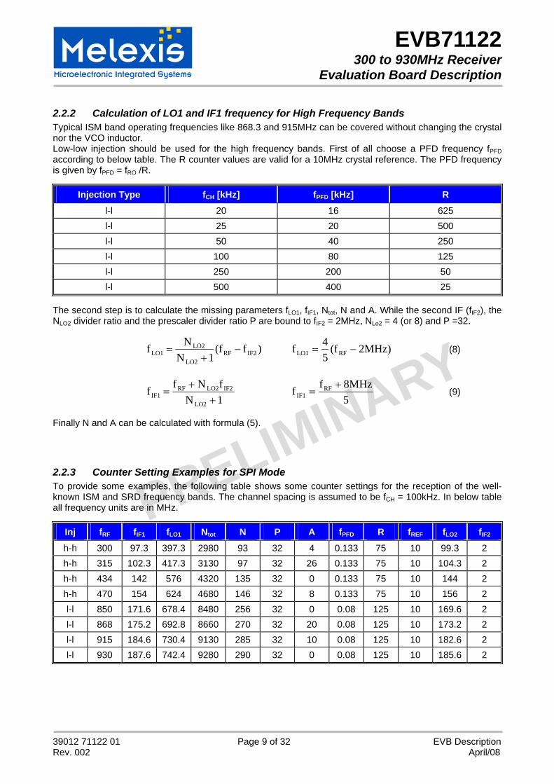
2.2.2 Calculation of LO1 and IF1 frequency for High Frequency Bands Typical ISM band operating frequencies like 868.3 and 915MHz can be covered without changing the crystal nor the VCO inductor. Low-low injection should be used for the high frequency bands. First of all choose a PFD frequency fPFD according to below table. The R counter values are valid for a 10MHz crystal reference. The PFD frequency is given by fPFD = fRO /R.
Injection Type fCH [kHz] fPFD [kHz] R l-l 20 16 625 l-l 25 20 500 l-l 50 40 250 l-l 100 80 125 l-l 250 200 50 l-l 500 400 25
The second step is to calculate the missing parameters fLO1, fIF1, Ntot, N and A. While the second IF (fIF2), the NLO2 divider ratio and the prescaler divider ratio P are bound to fIF2 = 2MHz, NLo2 = 4 (or 8) and P =32.
)f(f1N
Nf IF2RFLO2
LO2LO1 −
+= 2MHz)(f
54f RFLO1 −= (8)
1NfNff
LO2
IF2LO2RFIF1 +
+=
58MHzff RF
IF1+
= (9)
Finally N and A can be calculated with formula (5).
2.2.3 Counter Setting Examples for SPI Mode To provide some examples, the following table shows some counter settings for the reception of the well-known ISM and SRD frequency bands. The channel spacing is assumed to be fCH = 100kHz. In below table all frequency units are in MHz.
Inj fRF fIF1 fLO1 Ntot N P A fPFD R fREF fLO2 fIF2 h-h 300 97.3 397.3 2980 93 32 4 0.133 75 10 99.3 2 h-h 315 102.3 417.3 3130 97 32 26 0.133 75 10 104.3 2 h-h 434 142 576 4320 135 32 0 0.133 75 10 144 2 h-h 470 154 624 4680 146 32 8 0.133 75 10 156 2 l-l 850 171.6 678.4 8480 256 32 0 0.08 125 10 169.6 2 l-l 868 175.2 692.8 8660 270 32 20 0.08 125 10 173.2 2 l-l 915 184.6 730.4 9130 285 32 10 0.08 125 10 182.6 2 l-l 930 187.6 742.4 9280 290 32 0 0.08 125 10 185.6 2
PRI IN
EL MARY
EVB71122 300 to 930MHz Receiver
Evaluation Board Description
39012 71122 01 Page 10 of 32 EVB Description Rev. 002 April/08
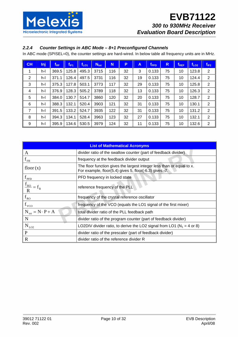
2.2.4 Counter Settings in ABC Mode – 8+1 Preconfigured Channels In ABC mode (SPISEL=0), the counter settings are hard-wired. In below table all frequency units are in MHz.
CH Inj fRF fIF1 fLO1 Ntot N P A fPFD R fREF fLO2 fIF2 1 h-l 369.5 125.8 495.3 3715 116 32 3 0.133 75 10 123.8 2 2 h-l 371.1 126.4 497.5 3731 116 32 19 0.133 75 10 124.4 2 3 h-l 375.3 127.8 503.1 3773 117 32 29 0.133 75 10 125.8 2 4 h-l 376.9 128.3 505.2 3789 118 32 13 0.133 75 10 126.3 2 5 h-l 384.0 130.7 514.7 3860 120 32 20 0.133 75 10 128.7 2 6 h-l 388.3 132.1 520.4 3903 121 32 31 0.133 75 10 130.1 2 7 h-l 391.5 133.2 524.7 3935 122 32 31 0.133 75 10 131.2 2 8 h-l 394.3 134.1 528.4 3963 123 32 27 0.133 75 10 132.1 2 9 h-l 395.9 134.6 530.5 3979 124 32 11 0.133 75 10 132.6 2
List of Mathematical Acronyms
A divider ratio of the swallow counter (part of feedback divider)
FBf frequency at the feedback divider output
(x)floor The floor function gives the largest integer less than or equal to x. For example, floor(5.4) gives 5, floor(-6.3) gives -7.
PFDf PFD frequency in locked state
RRO fR
f= reference frequency of the PLL
ROf frequency of the crystal reference oscillator
VCOf frequency of the VCO (equals the LO1 signal of the first mixer)
APNN tot +⋅= total divider ratio of the PLL feedback path
N divider ratio of the program counter (part of feedback divider)
LO2N LO2DIV divider ratio, to derive the LO2 signal from LO1 (N1 = 4 or 8)
P divider ratio of the prescaler (part of feedback divider) R divider ratio of the reference divider R
PRELIMINARY
EVB71122 300 to 930MHz Receiver
Evaluation Board Description
39012 71122 01 Page 11 of 32 EVB Description Rev. 002 April/08
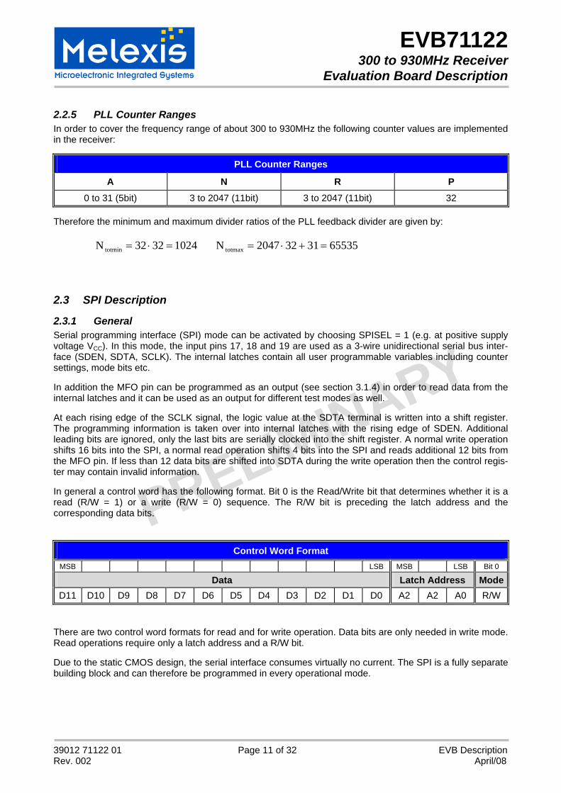
2.2.5 PLL Counter Ranges In order to cover the frequency range of about 300 to 930MHz the following counter values are implemented in the receiver:
PLL Counter Ranges
A N R P 0 to 31 (5bit) 3 to 2047 (11bit) 3 to 2047 (11bit) 32
Therefore the minimum and maximum divider ratios of the PLL feedback divider are given by: 10243232N totmin =⋅= 6553531322047N totmax =+⋅=
2.3 SPI Description
2.3.1 General Serial programming interface (SPI) mode can be activated by choosing SPISEL = 1 (e.g. at positive supply voltage VCC). In this mode, the input pins 17, 18 and 19 are used as a 3-wire unidirectional serial bus inter-face (SDEN, SDTA, SCLK). The internal latches contain all user programmable variables including counter settings, mode bits etc. In addition the MFO pin can be programmed as an output (see section 3.1.4) in order to read data from the internal latches and it can be used as an output for different test modes as well. At each rising edge of the SCLK signal, the logic value at the SDTA terminal is written into a shift register. The programming information is taken over into internal latches with the rising edge of SDEN. Additional leading bits are ignored, only the last bits are serially clocked into the shift register. A normal write operation shifts 16 bits into the SPI, a normal read operation shifts 4 bits into the SPI and reads additional 12 bits from the MFO pin. If less than 12 data bits are shifted into SDTA during the write operation then the control regis-ter may contain invalid information. In general a control word has the following format. Bit 0 is the Read/Write bit that determines whether it is a read (R/W = 1) or a write (R/W = 0) sequence. The R/W bit is preceding the latch address and the corresponding data bits.
Control Word Format MSB LSB MSB LSB Bit 0
Data Latch Address ModeD11 D10 D9 D8 D7 D6 D5 D4 D3 D2 D1 D0 A2 A2 A0 R/W
There are two control word formats for read and for write operation. Data bits are only needed in write mode. Read operations require only a latch address and a R/W bit. Due to the static CMOS design, the serial interface consumes virtually no current. The SPI is a fully separate building block and can therefore be programmed in every operational mode.
PRELIMINARY
EVB71122 300 to 930MHz Receiver
Evaluation Board Description
39012 71122 01 Page 12 of 32 EVB Description Rev. 002 April/08
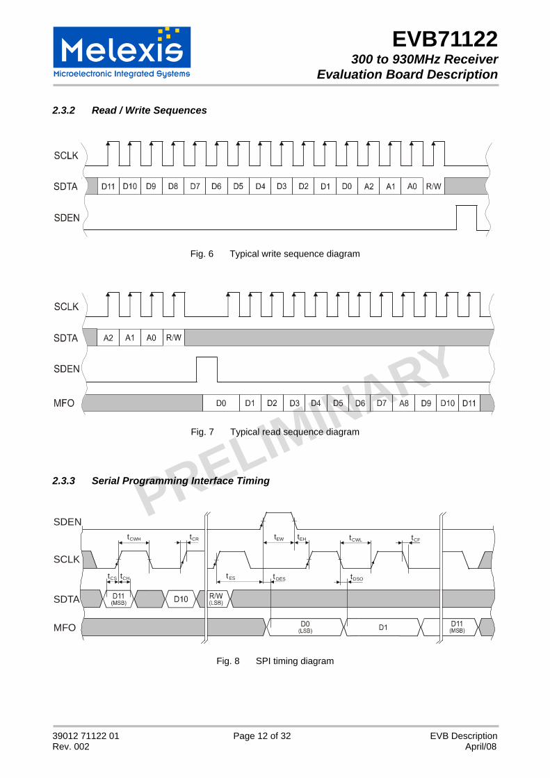
2.3.2 Read / Write Sequences
Fig. 6 Typical write sequence diagram
Fig. 7 Typical read sequence diagram
2.3.3 Serial Programming Interface Timing
tCWH tCR
tDSO
tCFtCWLtEW tEH
t DESt EStCS tCH
SDEN
SCLK
SDTA
MFO
Fig. 8 SPI timing diagram
PRELI I ARM N
Y
EVB71122 300 to 930MHz Receiver
Evaluation Board Description
39012 71122 01 Page 13 of 32 EVB Description Rev. 002 April/08
3 Register Description The following tables are to describe the functionality of the registers. Sec. 3.1 provides a register overview with all the control words R0 to R7. The subsequent sections. 3.1.1 to 3.1.8 show the content of the control words in more detail. Programming the registers requires SPI mode (SPISEL = 1). Default settings are for ABC mode.
3.1 Register Overview
DATA CONTROL WORD MSB LSB
LATCH ADDRESS
Bit No. 11 10 9 8 7 6 5 4 3 2 1 0 MSB LSB
default 0 0 0 0 1 0 0 0 1 1 0 0 0 0 0
R0
DTA
POL
SLC
SEL
SSB
SEL
DEM
GA
IN
IFFG
AIN
[ 1
:0 ]
MIX
2GA
IN
MIX
1GA
IN
LNA
GA
IN
[1 :
0 ]
OPM
OD
E
[ 1 :
0 ]
read/ write
Bit No. 11 10 9 8 7 6 5 4 3 2 1 0 MSB LSB
default 1 0 0 0 1 1 1 1 0 1 0 0 0 0 1
R1
SHO
WLD
PRES
CU
R
VCO
BU
F
VCO
CU
R
VCO
RA
NG
E
RSS
IGA
IN
LDTI
ME
[ 1
:0 ]
LDER
R
PFD
POL
CPC
UR
[ 1
: 0
]
read/ write
Bit No. 11 10 9 8 7 6 5 4 3 2 1 0 MSB LSB
default 1 1 1 1 0 0 0 1 0 1 0 0 0 1 0
R2 N
[ 6 :
0 ]
A
[ 4 :
0 ]
read/ write
Bit No. 11 10 9 8 7 6 5 4 3 2 1 0 MSB LSB
default 0 0 0 1 0 0 0 0 0 0 0 0 0 1 1
R3 MFO
[ 3
: 0
]
AG
CD
EL
[ 1 :
0 ]
AG
CEN
LO2D
IV
N
[ 10
: 7 ]
read/ write
PLIMI AR
REN
Y
EVB71122 300 to 930MHz Receiver
Evaluation Board Description
39012 71122 01 Page 14 of 32 EVB Description Rev. 002 April/08
DATA CONTROL WORD MSB LSB
LATCH ADDRESS
Bit No. 11 10 9 8 7 6 5 4 3 2 1 0 MSB LSB
default 0 0 0 0 0 1 0 0 1 0 1 1 1 0 0
R4
AG
CM
OD
E
R
[ 10
: 0 ]
read/ write
Bit No. 11 10 9 8 7 6 5 4 3 2 1 0 MSB LSB
default 0 0 1 0 1 0 1 0 1 1 0 0 1 0 1
R5
MO
DSE
L
RIF
F
[ 10
: 0 ]
read/ write
Bit No. 11 10 9 8 7 6 5 4 3 2 1 0 MSB LSB
default 1 1 1 0 1 0 0 0 0 1 0 1 1 1 0
R6
RO
CU
R
[ 1 :0
]
IFFT
UN
E
IFFH
LT
IFFP
RES
[ 7
: 0
]
read/ write
Bit No. 11 10 9 8 7 6 5 4 3 2 1 0 MSB LSB
default 1 1 1
R7
RSS
IH
LDR
SSIL
∗
IFFS
TATE
[ 1
:0 ]
IFFV
AL
[ 7
: 0
]
read- only
Note: ∗ depends on bit 11 in R4, 0 = RSSIL, 1 = LD
PRE IMAR
LIN
Y
EVB71122 300 to 930MHz Receiver
Evaluation Board Description
39012 71122 01 Page 15 of 32 EVB Description Rev. 002 April/08
3.1.1 Control Word R0
Name Bits Description operation mode
OPMODE [1:0] 00 01 10 11
shutdown receive mode reference oscillator & BIAS only synthesizer only
#default
LNA gain 00 01 10 11
lowest gain low gain high gain highest gain
(default – 20dB) (default – 6dB) (default – 2dB) (default – 0dB) #default
LNAGAIN [3:2]
gain values are relative to gain at default
1st Mixer gain MIX1GAIN [4] 0
1 high gain low gain
(14dB) (0dB)
#default
2nd Mixer gain MIX2GAIN [5] 0
1 high gain low gain
(9dB) (-2dB)
#default
intermediate frequency filter gain
IFFGAIN [7:6] 00 01 10 11
lowest gain low gain high gain highest gain
(-14dB) (-6dB) (0dB) (+6dB)
#default
demodulator gain DEMGAIN [8] 0
1 low gain high gain
(~ 12mV/kHz) (~ 14.5mV/kHz)
#default
single side band selection
0 1
upper side band lower side band
LO2 low-side inj. (IF1 = LO2 + IF2) LO2 high-side inj. (IF1 = LO2 – IF2)
#default SSBSEL [9]
Internal IF2 = 2MHz
slicer mode select SLCSEL [10] 0
1 averaging Data Slicer mode peak detector Data Slicer mode
#default
data output polarity OA2
0 inverted #default
‘1’ for space at ASK or fmin at FSK, ‘0’ for mark at ASK or fmax at FSK
1 normal
DTAPOL [11]
‘0’ for space at ASK or fmin at FSK, ‘1’ for mark at ASK or fmax at FSK
PRE IMIL
NARY
EVB71122 300 to 930MHz Receiver
Evaluation Board Description
39012 71122 01 Page 16 of 32 EVB Description Rev. 002 April/08
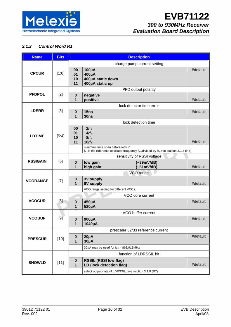
3.1.2 Control Word R1
Name Bits Description charge pump current setting
CPCUR [1:0] 00 01 10 11
100µA 400µA 400µA static down 400µA static up
#default
PFD output polarity PFDPOL [2] 0
1 negative positive #default
lock detector time error LDERR [3] 0
1 15ns 30ns
#default
lock detection time 00 01 10 11
2/fR 4/fR 8/fR 16/fR #default
LDTIME [5:4]
minimum time span before lock in fR is the reference oscillator frequency fRO divided by R, see section 3.1.5 (R4)
sensitivity of RSSI voltage RSSIGAIN [6] 0
1 low gain high gain
(~39mV/dB) (~51mV/dB) #default
VCO range 0 1
3V supply 5V supply #default VCORANGE [7]
VCO range setting for different VCCs.
VCO core current VCOCUR [8] 0
1 450µA 520µA
#default
VCO buffer current VCOBUF [9] 0
1 900µA 1040µA
#default
prescaler 32/33 reference current
0 1
20µA 30µA
#default PRESCUR [10]
30µA may be used for fRF = 868/915MHz
function of LDRSSIL bit
0 1
RSSIL (RSSI low flag) LD (lock detection flag) #default SHOWLD [11]
select output data of LDRSSIL, see section 3.1.8 (R7)
PRE IMI ARL
NY
EVB71122 300 to 930MHz Receiver
Evaluation Board Description
39012 71122 01 Page 17 of 32 EVB Description Rev. 002 April/08
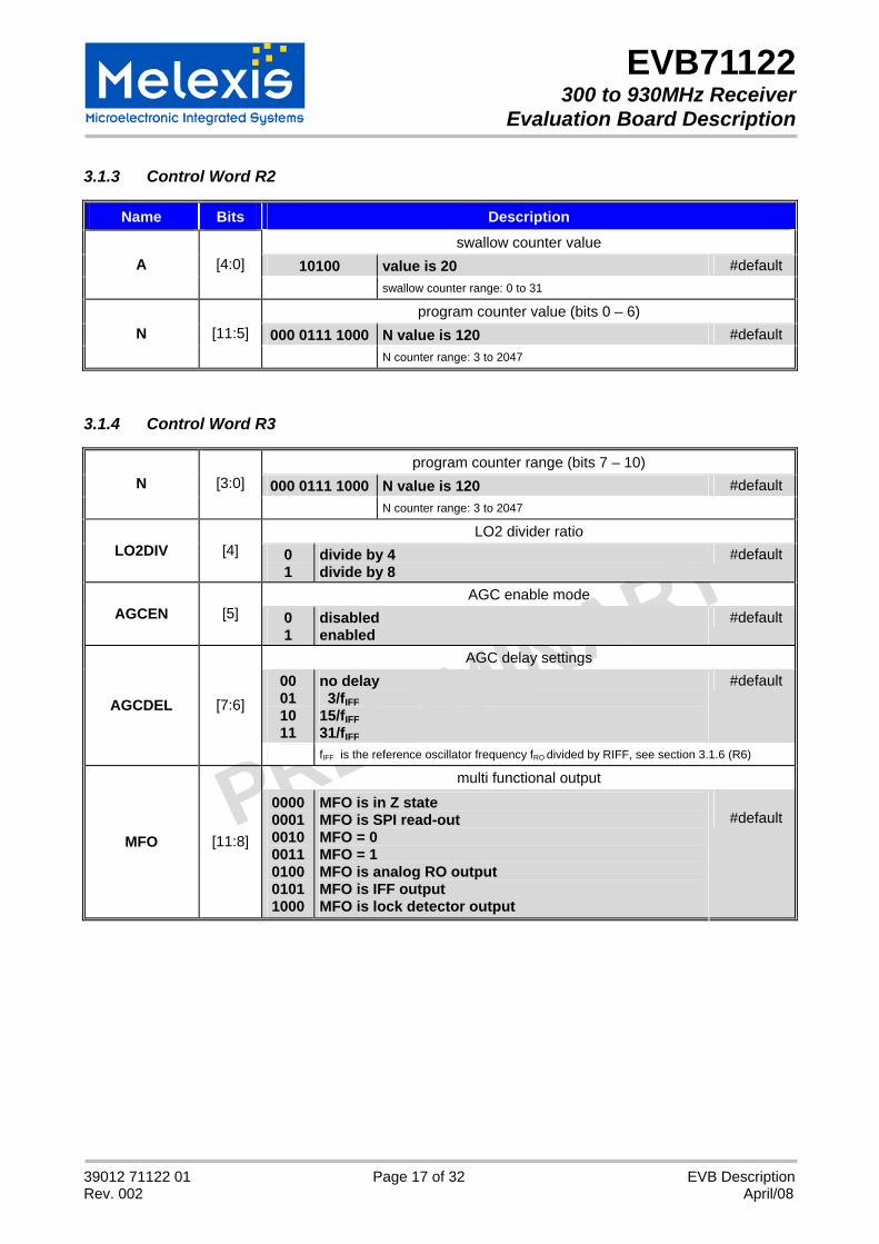
3.1.3 Control Word R2
Name Bits Description swallow counter value
10100 value is 20 #default A [4:0] swallow counter range: 0 to 31
program counter value (bits 0 – 6) 000 0111 1000 N value is 120 #default N [11:5]
N counter range: 3 to 2047
3.1.4 Control Word R3
program counter range (bits 7 – 10) 000 0111 1000 N value is 120 #default N [3:0]
N counter range: 3 to 2047
LO2 divider ratio LO2DIV [4] 0
1 divide by 4 divide by 8
#default
AGC enable mode AGCEN [5] 0
1 disabled enabled
#default
AGC delay settings 00 01 10 11
no delay 3/fIFF 15/fIFF 31/fIFF
#default
AGCDEL [7:6]
fIFF is the reference oscillator frequency fRO divided by RIFF, see section 3.1.6 (R6)
multi functional output
MFO [11:8]
0000 0001 0010 0011 0100 0101 1000
MFO is in Z state MFO is SPI read-out MFO = 0 MFO = 1 MFO is analog RO output MFO is IFF output MFO is lock detector output
#default
PRELIMINARY
EVB71122 300 to 930MHz Receiver
Evaluation Board Description
39012 71122 01 Page 18 of 32 EVB Description Rev. 002 April/08
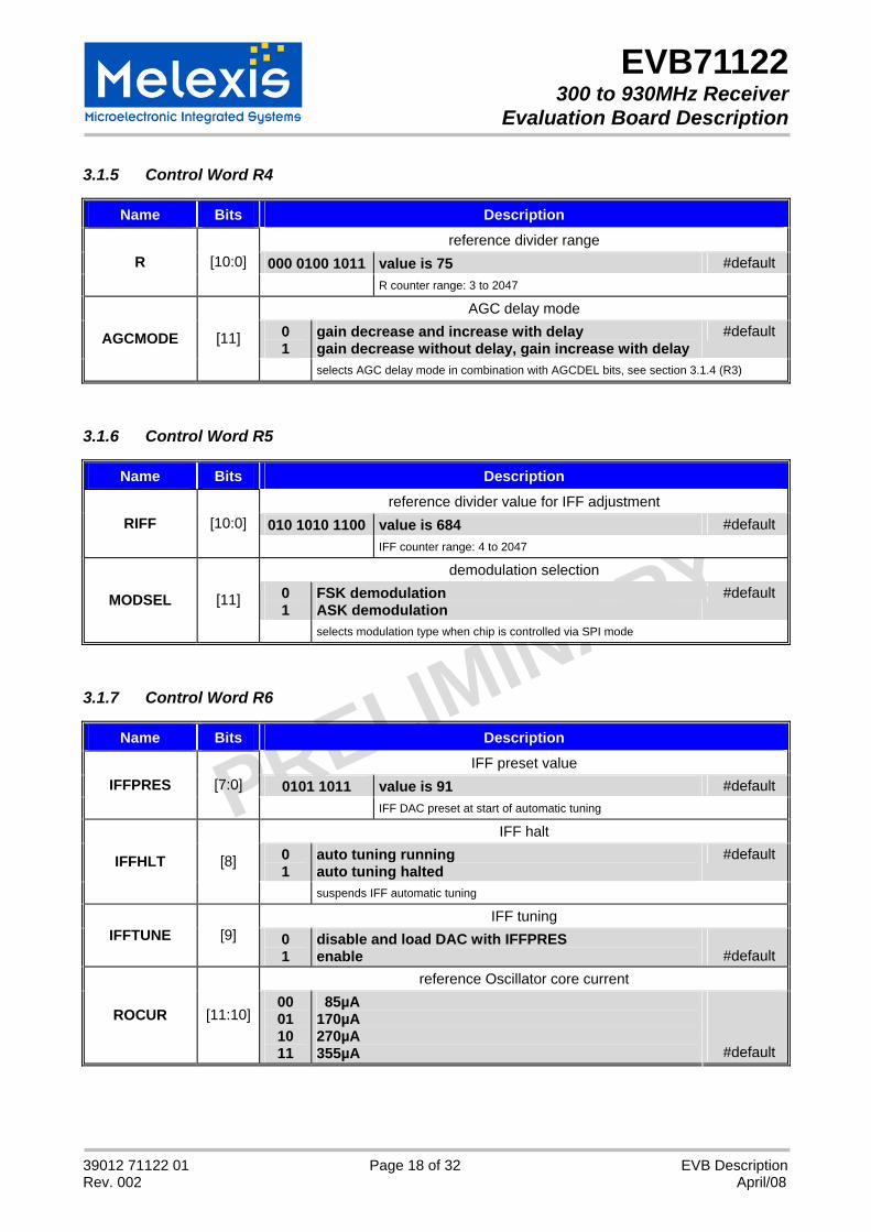
3.1.5 Control Word R4
Name Bits Description reference divider range
000 0100 1011 value is 75 #default R [10:0] R counter range: 3 to 2047
AGC delay mode 0 1
gain decrease and increase with delay gain decrease without delay, gain increase with delay
#default AGCMODE [11]
selects AGC delay mode in combination with AGCDEL bits, see section 3.1.4 (R3)
3.1.6 Control Word R5
Name Bits Description reference divider value for IFF adjustment
010 1010 1100 value is 684 #default RIFF [10:0] IFF counter range: 4 to 2047
demodulation selection 0 1
FSK demodulation ASK demodulation
#default MODSEL [11]
selects modulation type when chip is controlled via SPI mode
3.1.7 Control Word R6
Name Bits Description IFF preset value
0101 1011 value is 91 #default IFFPRES [7:0] IFF DAC preset at start of automatic tuning
IFF halt 0 1
auto tuning running auto tuning halted
#default IFFHLT [8]
suspends IFF automatic tuning
IFF tuning IFFTUNE [9] 0
1 disable and load DAC with IFFPRES enable #default
reference Oscillator core current
ROCUR [11:10] 00 01 10 11
85µA 170µA 270µA 355µA #default
PRELIMINARY
EVB71122 300 to 930MHz Receiver
Evaluation Board Description
39012 71122 01 Page 19 of 32 EVB Description Rev. 002 April/08
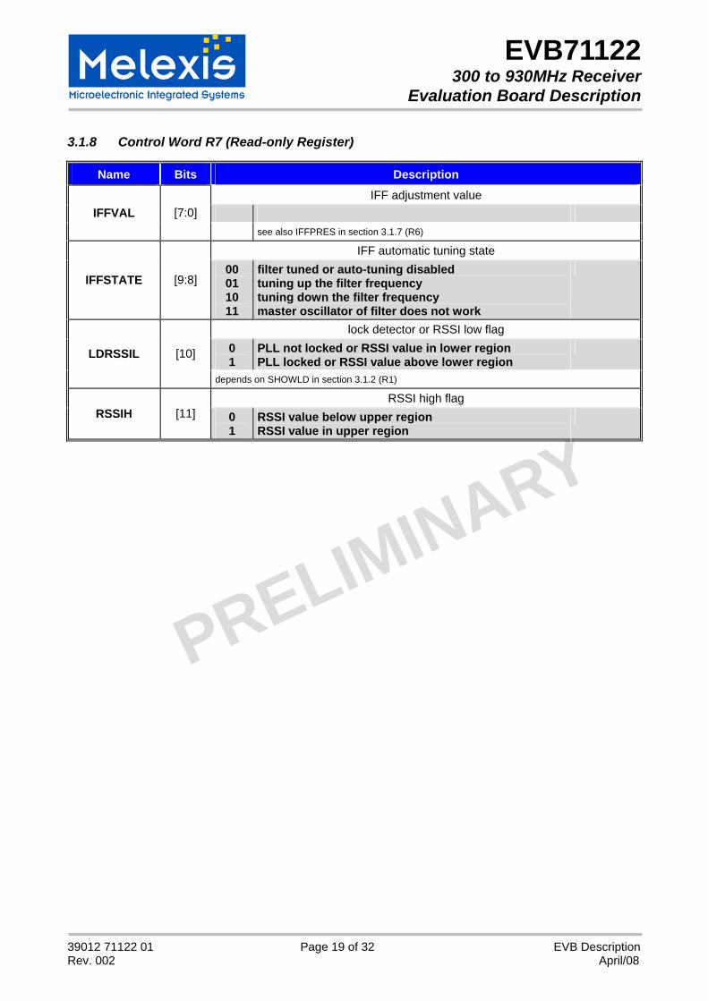
3.1.8 Control Word R7 (Read-only Register)
Name Bits Description IFF adjustment value
IFFVAL [7:0] see also IFFPRES in section 3.1.7 (R6)
IFF automatic tuning state
IFFSTATE [9:8] 00 01 10 11
filter tuned or auto-tuning disabled tuning up the filter frequency tuning down the filter frequency master oscillator of filter does not work
lock detector or RSSI low flag 0 1
PLL not locked or RSSI value in lower region PLL locked or RSSI value above lower region
LDRSSIL [10]
depends on SHOWLD in section 3.1.2 (R1)
RSSI high flag RSSIH [11] 0
1 RSSI value below upper region RSSI value in upper region
PRELIMINARY
EVB71122 300 to 930MHz Receiver
Evaluation Board Description
39012 71122 01 Page 20 of 32 EVB Description Rev. 002 April/08
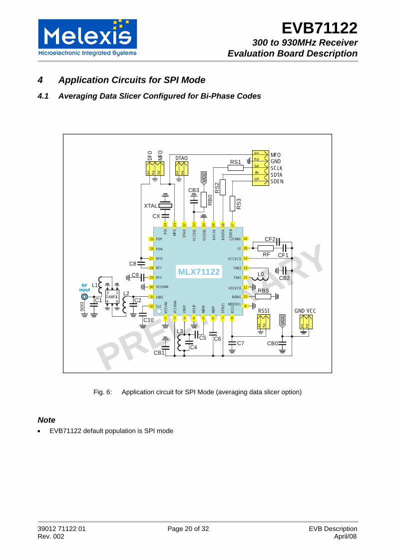
4 Application Circuits for SPI Mode 4.1 Averaging Data Slicer Configured for Bi-Phase Codes
MLX71122
1718192021222324
9
10
11
12
13
14
15
16
81 2 3 4 5 6 7
VEEL
NA
MFO
VEEI
F MODSEL
SPIS
EL
RSSI
RBIAS
DTAO
TNK1
TNK2
VCCVCO
VEEVCO
B/SD
TA
C/SD
ENROI
VCCD
IG
VEED
IG
LNAO
MIXN
MIXP
ENRX
LF
C6C5
C4
L3
L0
CB1
A/SC
LK
PDP
PDN
LNAI
27
25
31
26
DF2
SLC
C9
DFO
DF1
30
29
28C8
VEEANA
VCCA
NA
XTAL
CX
RBS
CB2
RF CF1
32
C10
RS1
RS2
RS
3
RB
0VC
C
CF2
CB3
VC
C
C7 CB0
DTAO
21
MFO
DFO
2 31
50
L1
C2L2
4 6
13
C1SAWFIL
45
12
3 GNDMFO
SDTASDEN
SCLK
RSSI
21
GND VCC
21
Fig. 6: Application circuit for SPI Mode (averaging data slicer option)
Note • EVB71122 default population is SPI mode

PRELIMINARY
EVB71122 300 to 930MHz Receiver
Evaluation Board Description
39012 71122 01 Page 21 of 32 EVB Description Rev. 002 April/08
Melexis GNDDTAOGNDGND MFODFO
FSK/ASK
MFO
SDTA
VCC
GNDGND
VCC
SDEN
B
C
SCLK
GND
ENRX
A
RSSI
MODSEL
EVB71122_002
CB
0
RF_input
RF_input
XTA
L1
3C
2 C7
C1
C8
CX
L1
L2
C10
00
RS2
RS1
RS3
RBS
RB
0
CF1
CF2
L0
RF
C5
C6
C4
L3
CB1
CB3
1
1
11
1
Board size is 49mm x 35.6mm
SPI mode selected
CB
2
Fig. 7: PCB Top-side view (averaging data slicer option)
PRELIMINARY
EVB71122 300 to 930MHz Receiver
Evaluation Board Description
39012 71122 01 Page 22 of 32 EVB Description Rev. 002 April/08
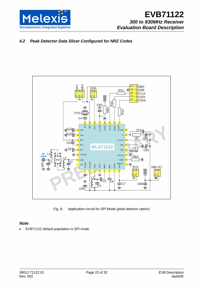
4.2 Peak Detector Data Slicer Configured for NRZ Codes
MLX71122
1718192021222324
9
10
11
12
13
14
15
16
81 2 3 4 5 6 7
VEEL
NA
MFO
VEEI
F MODSEL
SPIS
EL
RSSI
RBIAS
DTAO
TNK1
TNK2
VCCVCO
VEEVCO
B/SD
TA
C/SD
ENROI
VCCD
IG
VEED
IG
LNAO
MIXN
MIXP
ENRX
LF
C6C5
C4
L3
L0
CB1
A/SC
LK
PDP
PDN
LNAI
27
25
31
26
DF2
SLC
C9
DFO
DF1
30
29
28C8
VEEANA
VCCA
NA
CX
RBS
CB2
RF CF1
RS1
RS2
RS
3
RB
0VC
C
C11
C12CF2
CB3
VC
C
45
12
3 GNDMFO
SDTASDEN
SCLK
RSSI
21
C7 CB0
DTAO
21
50
L1
C2L2
4 6
13
C1SAWFIL
GND VCC
21
XTAL
MFO
DFO
2 31
Fig. 8: Application circuit for SPI Mode (peak detector option)
Note • EVB71122 default population is SPI mode
PRELIMINARY
EVB71122 300 to 930MHz Receiver
Evaluation Board Description
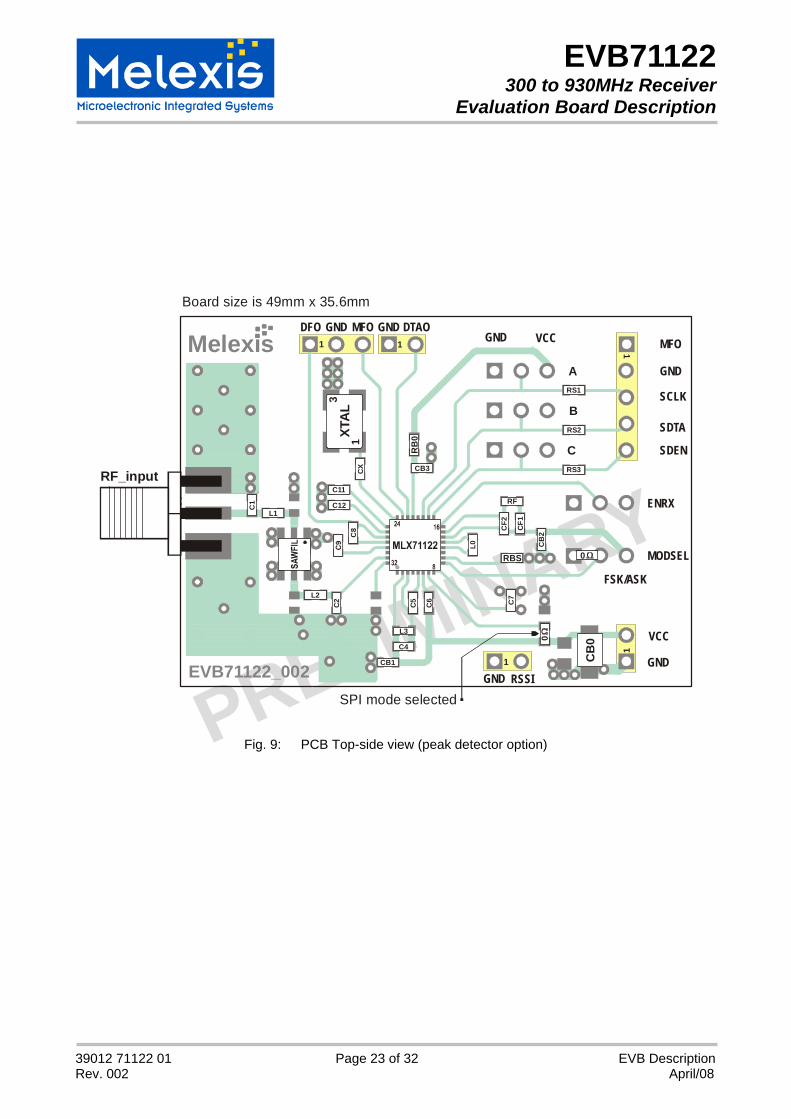
39012 71122 01 Page 23 of 32 EVB Description Rev. 002 April/08
Melexis GNDDTAOGNDGND MFODFO
FSK/ASK
MFO
SDTA
VCC
GNDGND
VCC
SDEN
B
C
SCLK
GND
ENRX
A
RSSI
MODSEL
EVB71122_002
CB
0
RF_input
RF_input
XTA
L1
3C
2 C7
C1
C8
CX
L1
L2
0
RS2
RS1
RS3
RBS
RB
0
CF1
CF2
L0
RF
CB
2
C5
C6
C4
L3
CB1
CB3
1
1
11
1
Board size is 49mm x 35.6mm
C11
C12
0
SPI mode selected
Fig. 9: PCB Top-side view (peak detector option)
P E I INAR
R L MY
EVB71122 300 to 930MHz Receiver
Evaluation Board Description
39012 71122 01 Page 24 of 32 EVB Description Rev. 002 April/08
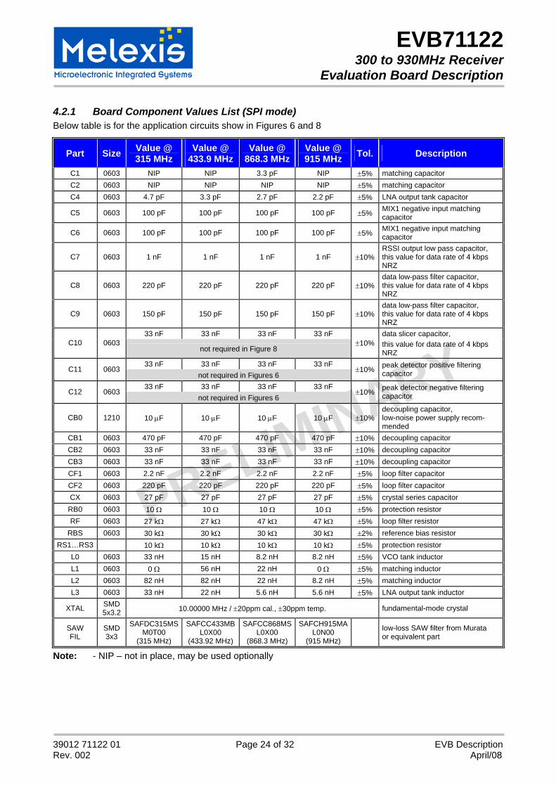
4.2.1 Board Component Values List (SPI mode) Below table is for the application circuits show in Figures 6 and 8
Part Size Value @ 315 MHz
Value @ 433.9 MHz
Value @ 868.3 MHz
Value @ 915 MHz Tol. Description
C1 0603 NIP NIP 3.3 pF NIP ±5% matching capacitor C2 0603 NIP NIP NIP NIP ±5% matching capacitor C4 0603 4.7 pF 3.3 pF 2.7 pF 2.2 pF ±5% LNA output tank capacitor
C5 0603 100 pF 100 pF 100 pF 100 pF ±5% MIX1 negative input matching capacitor
C6 0603 100 pF 100 pF 100 pF 100 pF ±5% MIX1 negative input matching capacitor
C7 0603 1 nF 1 nF 1 nF 1 nF ±10%RSSI output low pass capacitor, this value for data rate of 4 kbps NRZ
C8 0603 220 pF 220 pF 220 pF 220 pF ±10%data low-pass filter capacitor, this value for data rate of 4 kbps NRZ
C9 0603 150 pF 150 pF 150 pF 150 pF ±10%data low-pass filter capacitor, this value for data rate of 4 kbps NRZ
33 nF 33 nF 33 nF 33 nF C10 0603
not required in Figure 8 ±10%
data slicer capacitor, this value for data rate of 4 kbps NRZ
33 nF 33 nF 33 nF 33 nF C11 0603
not required in Figures 6 ±10% peak detector positive filtering
capacitor
33 nF 33 nF 33 nF 33 nF C12 0603
not required in Figures 6 ±10% peak detector negative filtering
capacitor
CB0 1210 10 μF 10 μF 10 μF 10 μF ±10%decoupling capacitor, low-noise power supply recom-mended
CB1 0603 470 pF 470 pF 470 pF 470 pF ±10% decoupling capacitor CB2 0603 33 nF 33 nF 33 nF 33 nF ±10% decoupling capacitor CB3 0603 33 nF 33 nF 33 nF 33 nF ±10% decoupling capacitor CF1 0603 2.2 nF 2.2 nF 2.2 nF 2.2 nF ±5% loop filter capacitor CF2 0603 220 pF 220 pF 220 pF 220 pF ±5% loop filter capacitor CX 0603 27 pF 27 pF 27 pF 27 pF ±5% crystal series capacitor
RB0 0603 10 Ω 10 Ω 10 Ω 10 Ω ±5% protection resistor RF 0603 27 kΩ 27 kΩ 47 kΩ 47 kΩ ±5% loop filter resistor
RBS 0603 30 kΩ 30 kΩ 30 kΩ 30 kΩ ±2% reference bias resistor RS1…RS3 10 kΩ 10 kΩ 10 kΩ 10 kΩ ±5% protection resistor
L0 0603 33 nH 15 nH 8.2 nH 8.2 nH ±5% VCO tank inductor L1 0603 0 Ω 56 nH 22 nH 0 Ω ±5% matching inductor L2 0603 82 nH 82 nH 22 nH 8.2 nH ±5% matching inductor L3 0603 33 nH 22 nH 5.6 nH 5.6 nH ±5% LNA output tank inductor
XTAL SMD 5x3.2 10.00000 MHz / ±20ppm cal., ±30ppm temp. fundamental-mode crystal
SAW FIL
SMD 3x3
SAFDC315MSM0T00
(315 MHz)
SAFCC433MBL0X00
(433.92 MHz)
SAFCC868MSL0X00
(868.3 MHz)
SAFCH915MAL0N00
(915 MHz)
low-loss SAW filter from Murata or equivalent part
Note: - NIP – not in place, may be used optionally
PRELIMINARY
EVB71122 300 to 930MHz Receiver
Evaluation Board Description
39012 71122 01 Page 25 of 32 EVB Description Rev. 002 April/08
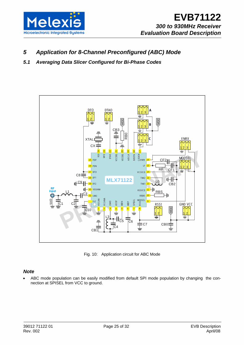
5 Application for 8-Channel Preconfigured (ABC) Mode 5.1 Averaging Data Slicer Configured for Bi-Phase Codes
32
C10
MLX71122
1718192021222324
9
10
11
12
13
14
15
16
81 2 3 4 5 6 7
VEEL
NA
MFO
VEEI
F MODSEL
SPIS
EL
RSSI
RBIAS
DTAO
TNK1
TNK2
VCCVCO
VEEVCO
B/SD
TA
C/SD
ENROI
VCCD
IG
VEED
IG
LNAO
MIX
N
MIX
P
ENRX
LF
C6C5
C4
L3
L0
CB1
A/SC
LK
PDP
PDN
LNAI
27
25
31
26
DF2
SLC
C9
DFO
DF1
30
29
28C8
VEEANA
VCCA
NA
CX
RBS
CB2
RF CF1
CF2
RB0
CB3B21 3
C21 3
A21 3
RSSI
21
21 3
21 3
MODSEL
ENRX
VC
C
VCC
C7
DTAO
21
CB0
VCC
GND VCC
21
C3L1
50 C2C1
XTAL
DFO
21
Fig. 10: Application circuit for ABC Mode
Note • ABC mode population can be easily modified from default SPI mode population by changing the con-
nection at SPISEL from VCC to ground.
PRELIMINARY
EVB71122 300 to 930MHz Receiver
Evaluation Board Description
39012 71122 01 Page 26 of 32 EVB Description Rev. 002 April/08
Melexis GNDDTAOGNDGND MFODFO
FSK/ASK
MFO
SDTA
VCC
GNDGND
VCC
SDEN
B
C
SCLK
GND
ENRX
A
RSSI
MODSEL
EVB71122_002
CB
0
RF_input
RF_input
XTA
L1
3
C2
C7
C1
C8
CX
L1
C10
RBS
RB
0
CF1
CF2
L0
RF
CB
2
C5
C6
C4
L3
C3
CB1
CB3
1
1
11
1
Board size is 49mm x 35.6mm
1
1
1
1
1
0
0
ABC mode selected
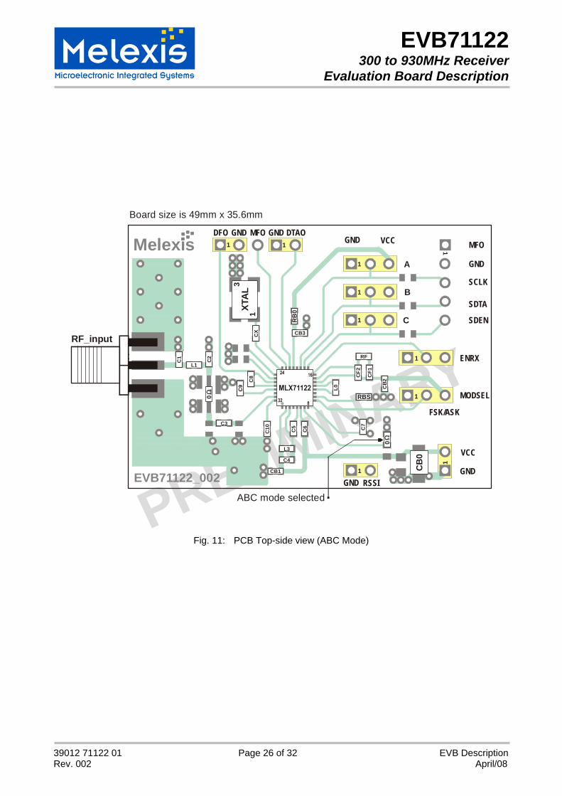
Fig. 11: PCB Top-side view (ABC Mode)
PRELIMINARY
EVB71122 300 to 930MHz Receiver
Evaluation Board Description
39012 71122 01 Page 27 of 32 EVB Description Rev. 002 April/08
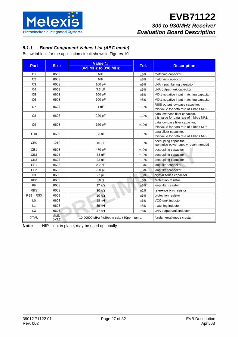
5.1.1 Board Component Values List (ABC mode) Below table is for the application circuit shows in Figures 10
Part Size Value @ 369 MHz to 396 MHz Tol. Description
C1 0603 NIP ±5% matching capacitor C2 0603 NIP ±5% matching capacitor C3 0603 100 pF ±5% LNA input filtering capacitor C4 0603 3.3 pF ±5% LNA output tank capacitor C5 0603 100 pF ±5% MIX1 negative input matching capacitor C6 0603 100 pF ±5% MIX1 negative input matching capacitor
C7 0603 1 nF ±10% RSSI output low pass capacitor, this value for data rate of 4 kbps NRZ
C8 0603 220 pF ±10% data low-pass filter capacitor, this value for data rate of 4 kbps NRZ
C9 0603 150 pF ±10% data low-pass filter capacitor, this value for data rate of 4 kbps NRZ
C10 0603 33 nF ±10% data slicer capacitor, this value for data rate of 4 kbps NRZ
CB0 1210 10 μF ±10% decoupling capacitor, low-noise power supply recommended
CB1 0603 470 pF ±10% decoupling capacitor CB2 0603 33 nF ±10% decoupling capacitor CB3 0603 33 nF ±10% decoupling capacitor CF1 0603 2.2 nF ±5% loop filter capacitor CF2 0603 220 pF ±5% loop filter capacitor CX 0603 27 pF ±5% crystal series capacitor
RB0 0603 10 Ω ±5% protection resistor RF 0603 27 kΩ ±5% loop filter resistor
RBS 0603 30 kΩ ±2% reference bias resistor RS1…RS3 0603 10 kΩ ±5% protection resistor
L0 0603 18 nH ±5% VCO tank inductor L1 0603 39 nH ±5% matching inductor L3 0603 27 nH ±5% LNA output tank inductor
XTAL SMD 5x3.2 10.00000 MHz / ±20ppm cal., ±30ppm temp. fundamental-mode crystal
Note: - NIP – not in place, may be used optionally
PRELIMINARY
EVB71122 300 to 930MHz Receiver
Evaluation Board Description
39012 71122 01 Page 28 of 32 EVB Description Rev. 002 April/08
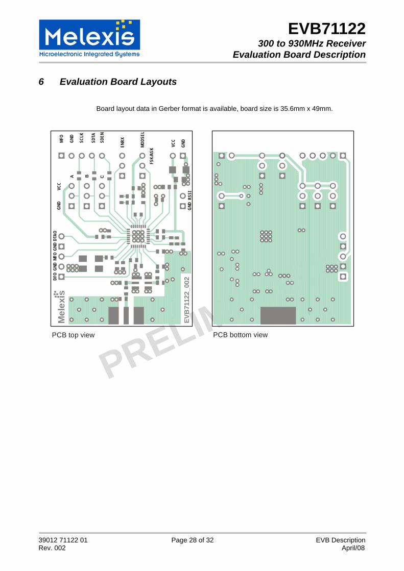
6 Evaluation Board Layouts
Board layout data in Gerber format is available, board size is 35.6mm x 49mm.
PCB top view PCB bottom view
Mel
exis
GND
DTAO
GND
GND
MFO
DFO
FSK/
ASK
MFO
SDTA
VCC
GND
GND
VCC
SDEN
B C
SCLK
GND
ENRX
A
RSSI
MODS
EL
EVB
7112
2_00
2
PRELIMINARY
EVB71122 300 to 930MHz Receiver
Evaluation Board Description
39012 71122 01 Page 29 of 32 EVB Description Rev. 002 April/08
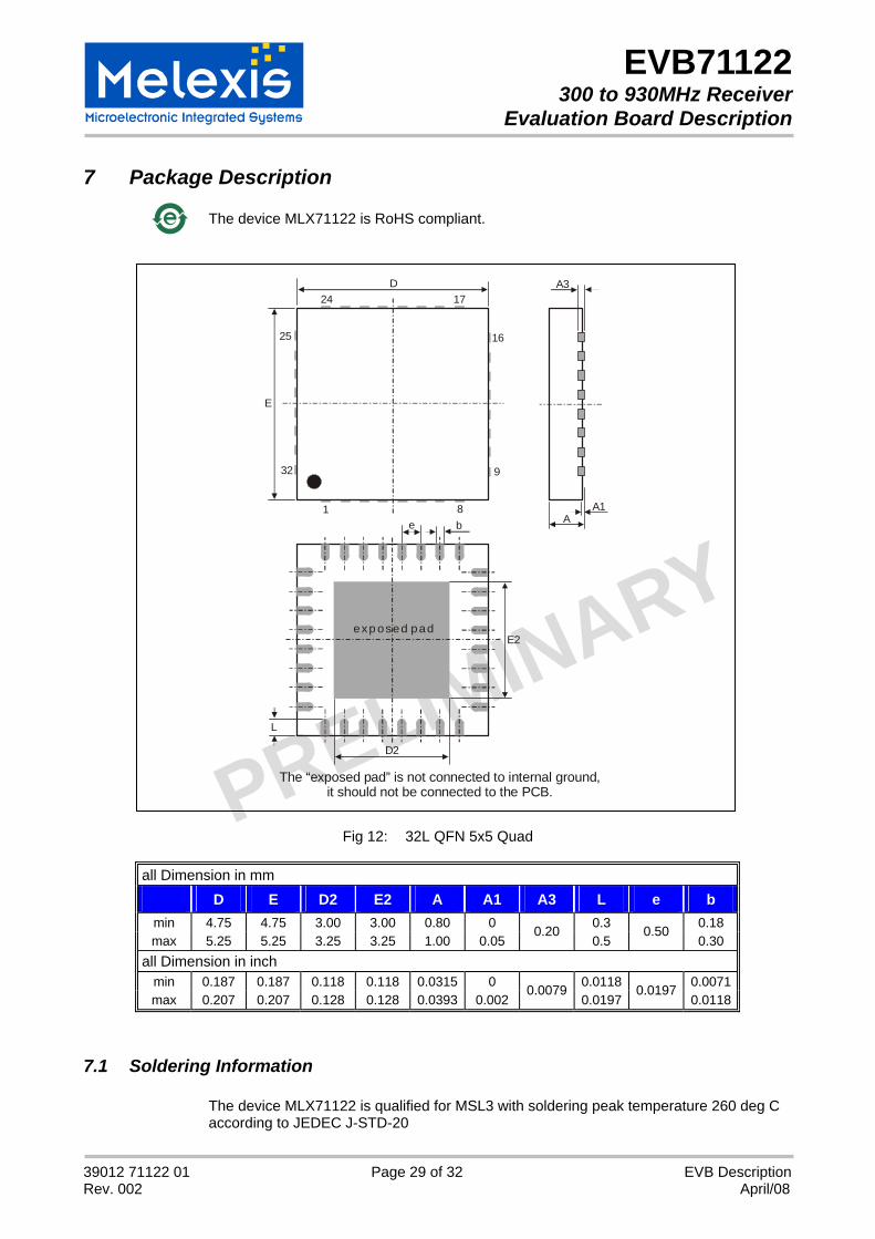
7 Package Description
The device MLX71122 is RoHS compliant.
A3
AA11 8
24 17
16
932
25
D
E
e b
L
D2
E2exp osed pad
The “exposed pad” is not connected to internal ground, it should not be connected to the PCB.
Fig 12: 32L QFN 5x5 Quad
all Dimension in mm
D E D2 E2 A A1 A3 L e b min 4.75 4.75 3.00 3.00 0.80 0 0.3 0.18 max 5.25 5.25 3.25 3.25 1.00 0.05
0.20 0.5
0.50 0.30
all Dimension in inch min 0.187 0.187 0.118 0.118 0.0315 0 0.0118 0.0071max 0.207 0.207 0.128 0.128 0.0393 0.002
0.00790.0197
0.0197 0.0118
7.1 Soldering Information
The device MLX71122 is qualified for MSL3 with soldering peak temperature 260 deg C according to JEDEC J-STD-20
PRIMINA
ELRY
EVB71122 300 to 930MHz Receiver
Evaluation Board Description
39012 71122 01 Page 30 of 32 EVB Description Rev. 002 April/08
8 Reliability Information This Melexis device is classified and qualified regarding soldering technology, solderability and moisture sensitivity level, as defined in this specification, according to following test methods: Reflow Soldering SMD’s (Surface Mount Devices)
• IPC/JEDEC J-STD-020 “Moisture/Reflow Sensitivity Classification for Nonhermetic Solid State Surface Mount Devices (classifi-cation reflow profiles according to table 5-2)”
Wave Soldering SMD’s (Surface Mount Devices)
• EN60749-20 “Resistance of plastic- encapsulated SMD’s to combined effect of moisture and soldering heat”
Solderability SMD’s (Surface Mount Devices)
• EIA/JEDEC JESD22-B102 “Solderability”
For all soldering technologies deviating from above mentioned standard conditions (regarding peak tempera-ture, temperature gradient, temperature profile etc) additional classification and qualification tests have to be agreed upon with Melexis.
The application of Wave Soldering for SMD’s is allowed only after consulting Melexis regarding assurance of adhesive strength between device and board.
9 ESD Precautions Electronic semiconductor products are sensitive to Electro Static Discharge (ESD). Always observe Electro Static Discharge control procedures whenever handling semiconductor products.
PRELIMINARY
EVB71122 300 to 930MHz Receiver
Evaluation Board Description
39012 71122 01 Page 31 of 32 EVB Description Rev. 002 April/08
Your Notes
PRELIMINARY
EVB71122 300 to 930MHz Receiver
Evaluation Board Description
39012 71122 01 Page 32 of 32 EVB Description Rev. 002 April/08
10 Disclaimer 1) The information included in this documentation is subject to Melexis intellectual and other property
rights. Reproduction of information is permissible only if the information will not be altered and is accom-panied by all associated conditions, limitations and notices.
2) Any use of the documentation without the prior written consent of Melexis other than the one set forth in
clause 1 is an unfair and deceptive business practice. Melexis is not responsible or liable for such al-tered documentation.
3) The information furnished by Melexis in this documentation is provided ’as is’. Except as expressly war-
ranted in any other applicable license agreement, Melexis disclaims all warranties either express, im-plied, statutory or otherwise including but not limited to the merchantability, fitness for a particular pur-pose, title and non-infringement with regard to the content of this documentation.
4) Notwithstanding the fact that Melexis endeavors to take care of the concept and content of this docu-
mentation, it may include technical or factual inaccuracies or typographical errors. Melexis disclaims any responsibility in connection herewith.
5) Melexis reserves the right to change the documentation, the specifications and prices at any time and
without notice. Therefore, prior to designing this product into a system, it is necessary to check with Melexis for current information.
6) Melexis shall not be liable to recipient or any third party for any damages, including but not limited to
personal injury, property damage, loss of profits, loss of use, interrupt of business or indirect, special in-cidental or consequential damages, of any kind, in connection with or arising out of the furnishing, per-formance or use of the information in this documentation.
7) The product described in this documentation is intended for use in normal commercial applications. Ap-
plications requiring operation beyond ranges specified in this documentation, unusual environmental re-quirements, or high reliability applications, such as military, medical life-support or life-sustaining equip-ment are specifically not recommended without additional processing by Melexis for each application.
8) Any supply of products by Melexis will be governed by the Melexis Terms of Sale, published on
www.melexis.com. © Melexis NV. All rights reserved.
For the latest version of this document, go to our website at: www.melexis.com
Or for additional information contact Melexis Direct:
Europe, Africa: Americas: Asia:
Phone: +32 1367 0495 Phone: +1 603 223 2362 Phone: +32 1367 0495 E-mail: [email protected] E-mail: [email protected] E-mail: [email protected]
ISO/TS 16949 and ISO14001 Certified