Embed Size (px)
Citation preview

Clif Fonstad, 9/29/09 Lecture 6 - Slide 1
• AnnouncementsFirst Hour Exam - Oct. 7, 7:30-9:30 pm; thru 10/2/09, PS #4
• ReviewMinority carrier flow in QNRs: 1. Lmin << w, 2. Lmin >> w
• I-V relationship for an abrupt p-n junctionAssume: 1. Low level injection
2. All applied voltage appears across junction:3. Majority carriers in quasi-equilibrium with barrier4. Negligible SCL generation and recombination
Relate minority populations at QNR edges, -xp and xn, to vABUse n'(-xp), p'(xn) to find hole and electron currents in QNRsConnect currents across SCL to get total junction current, iD
• Features and limitations of the modelEngineering the minority carrier injection across a junctionDeviations at low and high current levelsDeviations at large reverse bias
6.012 - Microelectronic Devices and CircuitsLecture 6 - p-n Junctions: I-V Relationship - Outline

Clif Fonstad, 9/29/09 Lecture 6 - Slide 2
QNR Flow: Uniform doping, non-uniform LL injection
We use the 5 QNR flow conditions* to simplify our 5 equations...(assuming a p-type sample)
!
q
"(x)p(x, t) # n(x, t) + Nd
+(x) # Na
#(x)[ ] =
dEx (x,t)
dx
!
Jh (x, t) = qµh p(x, t)E(x,t) " qDh
#p(x,t)
#x
!
Je (x, t) = qµen(x, t)E(x,t) + qDe
"n(x,t)
"x
!
"p(x, t)
"t+
1
q
"Jh (x,t)
"x="n(x,t)
"t#
1
q
"Je (x, t)
"x$ gL (x, t) # n(x,t)p(x, t) # ni
2[ ]r(t)
!
d2n'(x, t)
dx2
"n'(x, t)
De# e
= "1
De
gL (x, t)
..and end up with one equation in n': the static diffusion equation!
!
"1
q
dJh (x, t)
dx= #
1
q
dJe (x, t)
dx$ gL (x, t) #
n'(x, t)
% e
Quasi-static Quasi-static LLI
LLI
Uniform doping
Negligible minority driftQuasi-neutrality
!
" qµh po(x)E(x, t) # qDh
dn'(x, t)
dx
!
" Je (x, t) # qDe
dn'(x, t)
dx
!
"q
#p'(x,t) $ n'(x,t)[ ]
* Five assumptions that define flow problems AND should be validated at the end.

Clif Fonstad, 9/29/09 Lecture 6 - Slide 3
QNR Flow, cont.: Solving the steady state diffusion equation
The steady state diffusion equation in p-type material is:
and for n-type material it is:
!
d2n'(x)
dx2
"n'(x)
Le
2= "
1
De
gL (x)
!
d2p'(x)
dx2
"p'(x)
Lh
2= "
1
Dh
gL (x)
!
d2p'(x)
dx2
"p'(x)
Lh
2= 0
!
d2n'(x)
dx2
"n'(x)
Le
2= 0
In a basic p-n diode, we have gL = 0 which means we only needthe homogenous solutions, i.e. expressions that satisfy:
n-side: p-side:
!
Le " De# e
In writing these expressions we have introduced Le and Lh,the minority carrier diffusion lengths for holes andelectrons, as:
!
Lh " Dh# h
We'll see that the minority carrier diffusion length tells us howfar the average minority carrier diffuses before it recombines.

Clif Fonstad, 9/29/09 Lecture 6 - Slide 4
QNR Flow, cont.: Solving the steady state diffusion equation
We seldom care about this general result. Instead, we findthat most diodes fall into one of two cases:
Case I - Long-base diode: wn >> Lh
Case II - Short-base diode: Lh >> wn
Case I: When wn >> Lh, which is the situation in an LED, forexample, the solution is
!
p'(x) " p'(xn )e# x#xn( ) Lh for xn $ x $ wn
This profile decays from p'(xn) to 0 exponentially as e-x//Lh.
The corresponding hole current for xn ≤ x ≤ wn in Case I is
!
Jh (x) " #qDh
dp'(x)
dx=
qDh
Lh
p'(xn )e# x#xn( ) Lh for xn $ x $ wn
The current decays to zero also, indicating that all of the excessminority carriers have recombined before getting to the contact.

Clif Fonstad, 9/29/09 Lecture 6 - Slide 5
QNR Flow, cont.: Solving the steady state diffusion equation
Case II: When Lh >> wn, which is the situation in integratedSi diodes, for example, the differential equation simplifiesto:
We see immediately that p'(x) is linear:
!
d2p'(x)
dx2
=p'(x)
Lh
2" 0
!
p'(x) = A x + B
!
p'(x) " p'(xn ) 1#x # xn
wn # xn
$
% &
'
( )
*
+ ,
-
. / for xn 0 x 0 wn
This profile is a straight line, decreasing from p'(xn) at xn to 0 at wn.
Fitting the boundary conditions we find:
In Case II the current is constant for xn ≤ x ≤ wn:
!
Jh (x) " #qDh
dp'(x)
dx=
qDh
wn # xn
p'(xn ) for xn $ x $ wn
The constant current indicates that no carriers recombinebefore reaching the contact.

Clif Fonstad, 9/29/09 Lecture 6 - Slide 6
wn0 xn
p'n(x) [cm-3]
x [cm]
p'n(xn)
Case II - Short base: wn << Ln (the situation in most Si diodes and transistors)
x [cm]wn0 xn
Jh(x) [A/cm2]
qDhp'n(xn) [wn-xn]
QNR Flow, cont.: Uniform doping, non-uniform LL injection
Case I - Long base: wn >> Ln (the situation in LEDs)
x [cm]wn
Jh(x) [A/cm2]
qDhp'n(xn) Lhe-x/Lh
0 xn xn+Lhwn0 xn xn+Lh
p'n(x) [cm-3]
x [cm]
p'n(xn)e-x/Lh
Sketching and comparing the limiting cases: wn>>Lh, wn<<Lh

Clif Fonstad, 9/29/09 Lecture 6 - Slide 7
The four other unknowns⇒ In n-type the steady state diffusion equation gives p’.⇒ Knowing p', we can easily get n’, Je, Jh, and Ex:
QNR Flow, cont.: Uniform doping, non-uniform LL injection
!
Ex (x) "1
qµeno
Je (x) +De
Dh
Jh (x)#
$ %
&
' ( Next find Ex:
!
n'(x) " p'(x) #$
q
dEx (x)
dxThen find n’:
Finally, go back and check that all of the five conditions aremet by the solution.
!
Jh (x) " # qDh
dp'(x)
dxFirst find Jh:
!
Je (x) = JTot " Jh (x)Then find Je:
Once we solve the diffusion equation and getthe minority carrier excess we know everything.
Note: In Lec 5 we saw thisfor a p-type sample.
Clif Fonstad, 9/29/09 Lecture 6 - Slide 8
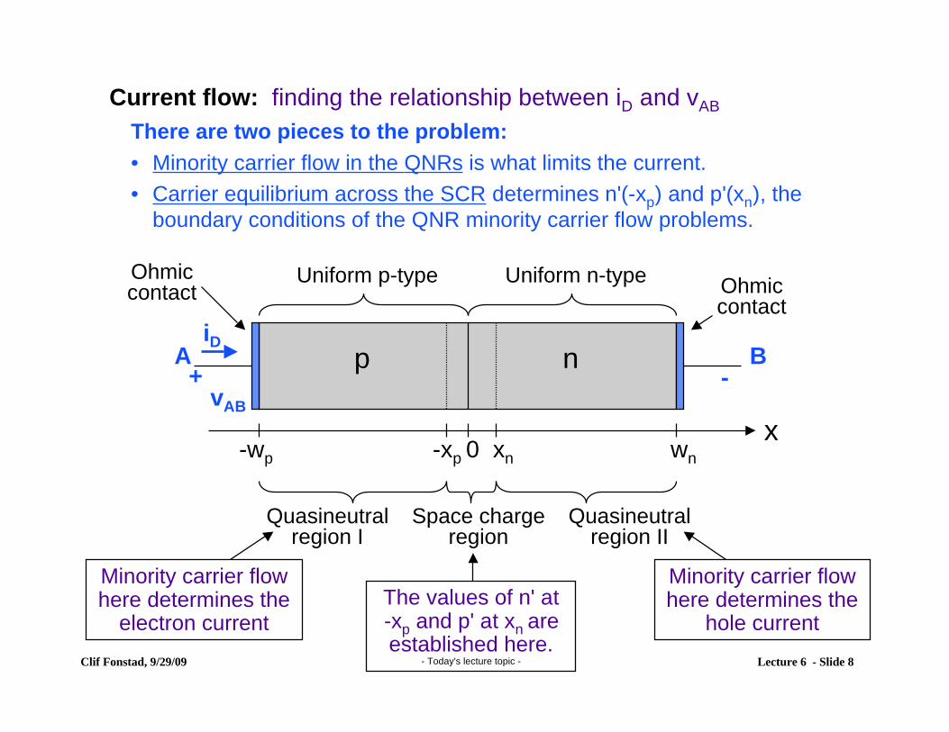
There are two pieces to the problem:• Minority carrier flow in the QNRs is what limits the current.• Carrier equilibrium across the SCR determines n'(-xp) and p'(xn), the
boundary conditions of the QNR minority carrier flow problems.
p n
Uniform p-type Uniform n-type
-wpx
wn -xp 0 xn
Ohmiccontact
Ohmiccontact
A BiD
+ -vAB
Quasineutralregion I
Quasineutralregion II
Space chargeregion
Minority carrier flowhere determines the
electron current
Minority carrier flowhere determines the
hole currentThe values of n' at-xp and p' at xn areestablished here.
- Today's lecture topic -
Current flow: finding the relationship between iD and vAB

Clif Fonstad, 9/29/09 Lecture 6 - Slide 9
The p-n Junction Diode: the game plan for getting iD(vAB)We have two QNR's and a flow problem in each:
n
xwn0 xn
Ohmiccontact
B-
Quasineutralregion II
x
p
Ohmiccontact
AiD
+vAB
Quasineutralregion I
-wp -xp 0
-wp -xp 0 wn0 xn
n'p p'n
n'(-wp) = 0
n'(-xp) = ?
p'(wn) = 0p'(xn) = ?
If we knew n'(-xp) and p'(xn), we could solve the flow problemsand we could get n'(x) for -wp<x<-xp, and p'(x) for xn<x<wn …
xx

Clif Fonstad, 9/29/09 Lecture 6 - Slide 10
….and knowing n'(x) for -wp<x<-xp, and p'(x) for xn<x<wn, we canfind Je(x) for -wp<x<-xp, and Jh(x) for xn<x<wn.
-wp -xp 0 wn0 xn
n'p p'n
n'(-wp) = 0
n'(-xp,vAB) = ?
p'(wn) = 0p'(xn,vAB) = ?
Having Je(x) for -wp<x<-xp, and Jh(x) for xn<x<wn, we can get iDbecause we will argue that iD(vAB) = A[Je(-xp,vAB)+Jh(xn,vAB)]… …but first we need to know n'(-xp,vAB) and p'(xn,vAB).
We will do this now.
wn0 xn-wp -xp 0
Je JhJe(-wp<x<-xp)=qDe(dn'/dx)Jh(xn<x<wn)=-qDh(dp'/dx)
xx
xx

Clif Fonstad, 9/29/09 Lecture 6 - Slide 11
The impact of the barrier height change on the carrier populationsand fluxes:
qφ
x
Reverse biason junctionBarrier raised so
the few carriers ontop spill back down.
qφ
x
Forward biason junction
Barrier lowered socarriers to left can
cross over it.The flux is limitedby how fast they
diffuse in the QNR.
qφ
x
Unbiasedjunction
Population inequilibrium with
barrier

Clif Fonstad, 9/29/09 Lecture 6 - Slide 12
!
po x " #xp( ) = nie#q$ p kT
= NAp
!
po x " xn( ) = nie#q$n kT = ni
2NDn
!
po(xp < x < xn ) = nie"q# (x ) kT
-xp xn
!
q"B
Hol
e po
tent
ial e
nerg
y, qφ
Majority carriers against the junction barrierZero applied bias, vAB = 0; thermal equilibrium barrier
!
po x " xn( ) = nie#q$n kT = NApe
#q $n#$ p( ) kT= NApe
#q$B kTNotice that:
"The holes are in equilibrium with the barrier."

Clif Fonstad, 9/29/09 Lecture 6 - Slide 13
Boundary condtions at the edges of the space charge layer:What are n’(-xp) and p’(xn)?
YES, we do, and the Boltzman relationship holds.
If the population of holes at the topof the potential “hill” is related tothe population at the bottom by aBoltzman factor, then we shouldalso find that:
Do we?
Begin by looking at the situation in thermal equilibrium,where we have:
!
"b =kT
qln
NApNDn
ni
2#
ni
2
NDn
= NApe$q"b / kT
Thus : po(xn ) =ni
2
NDn
= NApe$q"b / kT = po($xp )e
$q"b / kT
x-xp xn0
qφ
qφb
!
po(xn ) = po("xp )e"q#b / kT
!
po("xp ) = NAp and po(xn ) = ni
2NDn

Clif Fonstad, 9/29/09 Lecture 6 - Slide 14
Hol
e po
tent
ial e
nerg
y, qφ
!
po x " #xp( ) $ NAp
!
po x >> xn( ) =
ni
2NDn
!
p xn( ) > ni
2NDn
-xp xn
Majority carriers against the junction barrier Forward bias, vAB > 0; barrier lowered, carriers spill over
We say the holes are still in equilibrium with the barrier at xn:
!
p xn( ) = NApe"q #B "vAB( ) kT
=ni
2
NDn
e+qvAB kT
!
q "B # vAB( )

Clif Fonstad, 9/29/09 Lecture 6 - Slide 15
Majority carriers against the junction barrier Reverse bias, vAB < 0; barrier raised, carriers spill back
Hol
e po
tent
ial e
nerg
y, qφ
!
p x < "xp( ) # NAp
!
p x >> xn( ) =
ni
2NDn
!
p xn( ) < ni
2NDn
-xp xnAgain the holes maintain equilibrium with the barrier until xn:
!
p xn( ) = NApe"q #B "vAB( ) kT
=ni
2
NDn
e+qvAB kT
And we have the same expression for p(xn).
!
q "B # vAB( )

Clif Fonstad, 9/29/09 Lecture 6 - Slide 16
What are n’(-xp) and p’(xn) with vAB applied?
We propose that the majority carrier populations on either sideare still related by the Boltzman factor,* which is now:exp[-q(φb-vAB)/kT]
Thus:
Under low level injection conditions, the majority carrierpopulation is unchanged, so p(-xp) remains NAp, so:
And the excess population we seek is:
Similarly at -xp:
!
p(xn ) = p("xp )e"q #b "vAB[ ] / kT
!
p(xn ) = NAp e"q #b "vAB[ ] / kT
=ni
2
NDn
eqvAB / kT
!
p'(xn ) = p(xn ) " pon =ni
2
NDn
eqvAB / kT
"1( )
!
n'("xp ) =ni
2
NAp
eqvAB / kT
"1( )
* We are assuming that the majority carriers can get acrossthe SCL much faster than they can diffuse away as minoritycarriers, i.e., that diffusion is the bottleneck!

Clif Fonstad, 9/29/09 Lecture 6 - Slide 17
What is the current, iD?
Biased p-n junctions: current flow, cont.
Knowing p’(xn) and n’(-xp), we know:
But we still don’t know the total current because we don’tknow both currents at the same position, x:
To proceed we make the assumption that there is negligiblerecombination of holes and electrons in the depletionregion, so what goes in comes out and:
With this assumption, we can write:
!
Jh(x) for xn < x < wn
andJ
e(x) for - w p < x < "xp
!
iD
= A JTOT = A Jh (x) + Je (x)[ ]
!
Jh(xn ) = J
h("xp ) and J
e(xn ) = J
e("xp )
!
iD
= A JTOT = A Jh (xn ) + Je ("xp )[ ]
Have to be at same “x”
Values at edges of SCL

Clif Fonstad, 9/29/09 Lecture 6 - Slide 18
What is the current, iD, cont,?
Biased p-n junctions: current flow, cont.
Both Jh(xn) and Je(-xp), are proportional to p’(xn) and n’(-xp),respectively, which in turn are both proportional to (eqv/kT -1):
Thus the diode current is also proportional to (eqv/kT -1):
(IS is called the reverse saturation current of the diode.)
!
Jh(x
n)"p'(x
n)" e
qv AB / kT-1[ ] and J
e(-x
p)"n'(x
p)" e
qv AB / kT-1[ ]
!
iD
= A Jh (xn ) + Je ("xp )[ ] # eqvAB / kT
"1[ ] $ iD
= Is eqvAB / kT
"1[ ]
** Notice: The non-linearity, i.e., the exponential dependence of thediode current on voltage, arises because of the exponentialdependence of the minority carrier populations the edges of thespace charge layer (depletion region). The flow problemsthemselves are linear.

Clif Fonstad, 9/29/09 Lecture 6 - Slide 19
The saturation current of three diode types:IS's dependence on the relative sizes of w and Lmin
Biased p-n junctions: current flow, cont.
Short-base diode, wn << Lh, wp << Le:
!
Jh(x
n) = q
ni
2
NDn
Dh
wn " xn( )e
qv AB / kT-1[ ]
Je(-x
p) = q
ni
2
NAp
De
wp " xp( )e
qv AB / kT-1[ ]
#
$
% %
&
% %
iD
= Aqni
2 Dh
NDn wn " xn( )+
De
NAp wp " xp( )
'
( ) )
*
+ , ,
eqv AB / kT
-1[ ]
p’(x), n’(x)
x xn-xp -wp wn
n’(-xp)
p’(xn)
!
Jh(x
n) = q
ni
2
NDn
Dh
Lh
eqv AB / kT
-1[ ]
Je(-x
p) = q
ni
2
NAp
De
Le
eqv AB / kT
-1[ ]
"
#
$ $
%
$ $
iD
= Aqni
2 Dh
NDnLh
+De
NApLe
&
' (
)
* + e
qv AB / kT-1[ ]
p’(x), n’(x)
x xn-xp -wp wn
n’(-xp)
p’(xn)
Long-base diode, wn >> Lh, wp >> Le:
!
iD
= Aqni
2 Dh
NDnwn,eff
+De
NApwp,eff
"
# $
%
& ' e
qv AB / kT-1[ ]
Hole injection into n-side Electron injection into p-side
General diode:
!
Note : wn,eff " Lh tanh wn - xn( ), wp,eff " Le tanh wp - xp( )

Clif Fonstad, 9/29/09 Lecture 6 - Slide 20
The ideal exponential diode
Biased p-n junctions: current flow, cont.
• General expression: iD = IS(eqVAB/kT - 1)
• Forward bias, |vAB| > kT/q: iD ≈ ISeqVAB/kT
Current increases 10xfor every 60 mV in-crease in vAB.
• Reverse bias, |vAB| > kT/q:Current saturates at IS.
iD = - IS
Ref: Adapted from Figure 18 in S. M. Sze, “Physicsof Semiconductor Devices” 1st. Ed (Wiley, 1969)
108
107
106
105
104
103
102
101
100
10-10 5 10 15 20 25 30
q|v|/kT
|J/Js|
Ideal forward
Ideal reverse
60 mV/decade
Js
Figure by MIT OpenCourseWare.

Clif Fonstad, 9/29/09 Lecture 6 - Slide 21
Limitations of the modelNOTE: This figure is a bit exagerated,
but it makes the point.
Biased p-n junctions: current flow, cont.
• Large forward bias:Sub-exponential increase- High level injection (c)- Series voltage drop (d)
• Large reverse bias:Abrupt, rapid increase- Non-destructive break- down
• Very low bias levels:Excess current seen- SCL generation and recombination (a, e)
Ref: Figure 18 in S. M. Sze, “Physics of Semi-conductor Devices” 1st. Ed (Wiley, 1969)
108
107
106
105
104
103
102
101
100
10-10 5 10 15 20 25 30
q|v|/kT
|J/Js|
Ideal forward
Junction breakdown
Ideal reverse
Forward
Reverse
(a)(e)
(b)
(d)
(c)
Figure by MIT OpenCourseWare.

Clif Fonstad, 9/29/09 Lecture 6 - Slide 22
Asymmetrically doped junctions: an important special case
Depletion region impacts/issues
A p+-n junction (NAp >> NDn):
An n+-p junction (NDn >> NAp):
Note that in both cases the depletion region is predominately on thelightly doped side, and it is the doping level of the more lightly dopedjunction that matters (i.e., dominates).
Note also that as the doping level increases the depletion widthdecreases and the peak E-field increases. [This is also true insymmetrical diodes.]
!
xn >> xp , w " xn "2#Si $b % vAB( )
qNDn
, E pk "2q $b % vAB( )NDn
#Si
!
xp >> xn , w " xp "2#Si $b % vAB( )
qNAp
, E pk "2q $b % vAB( )NAp
#Si
!
NApNDn NAp + NDn( ) " NDn
!
NApNDn NAp + NDn( ) " NAp
Two very important and useful observations!!

Clif Fonstad, 9/29/09 Lecture 6 - Slide 23
Asymmetrically doped junctions: an important special case
Current flow impact/issues
!
" Aqni
2 Dh
NDnwn,eff
eqv AB / kT
-1[ ]
Hole injection into n-side
A p+-n junction (NAp >> NDn):
!
iD
= Aqni
2 Dh
NDnwn,eff
+De
NApwp,eff
"
# $
%
& ' e
qv AB / kT-1[ ] ( Aqn
i
2 De
NApwp,eff
eqv AB / kT
-1[ ]
Electron injection into p-side
An n+-p junction (NDn >> NAp):
Two very important and useful observations!!
Note that in both cases the minority carrier injection is predominately intothe lightly doped side.
Note also that it is the doping level of the more lightly doped junction thatdetermines the magnitude of the current, and as the doping level on thelightly doped side decreases, the magnitude of the current increases.
!
iD
= Aqni
2 Dh
NDnwn,eff
+De
NApwp,eff
"
# $
%
& ' e
qv AB / kT-1[ ]

Clif Fonstad, 9/29/09 Lecture 6 - Slide 24
6.012 - Microelectronic Devices and CircuitsLecture 6 - p-n Junctions: I-V Relationship - Summary
• I-V relationship for an abrupt p-n junctionFocus is on minority carrier diffusion on either side of SCLVoltage across SCL sets excess populations -xp and xn:
n'(-xp) = nnoe-q[fb – vAB]/kT-npo = npo(eqvAB/kT-1) = (ni2/NAp)(eqvAB/kT -1)
p'(xn) = ppoe-q[fb – vAB]/kT-pno = pno(eqvAB/kT-1) = (ni2/NDn)(eqvAB/kT -1)
Flow problems in QNR regions give minority currents: Je(-wp<x<-xp) = q(De/Le)[cosh(wp-x)/sinh(wp-xp)](ni
2/NAp)(eqvAB/kT -1) Jh(xn<x<wn) = q(Dh/Lh)[cosh(wn-x)/sinh(wn-xn)](ni
2/NDn)(eqvAB/kT -1)Total current is found from continuity across SCL:
iD(vAB) = A [Je(-xp) + Jh(xn)] = IS (eqvAB/kT -1), withIS ≡A q ni
2 [(Dh/NDn wn*) + (De/NAp wp
*)] (hole component) (electron component)
Note: wp* and wn
* are the effective widths of the p- and n-sidesIf Le >> wp, then wp* ≈ (wp - xp), and if Le << wp, then wp* ≈ LeIf Lh >> wn, then wn* ≈ (wn - xn), and if Lh << wn, then wn* ≈ Lh
• Features and limitations of the modelExponential dependence enters via boundary conditionsInjection is predominantly into more lightly doped sideSaturation current, IS, goes down as doping levels go upLimits: 1. SCL g-r may dominate at low current levels
2. Series resistance may reduce junction voltage at high currents3. Junction may breakdown (conduct) at large reverse bias

MIT OpenCourseWarehttp://ocw.mit.edu
6.012 Microelectronic Devices and Circuits Fall 2009
For information about citing these materials or our Terms of Use, visit: http://ocw.mit.edu/terms.