Embed Size (px)
Citation preview

PE..scq~p (.( b / I" A..( d I~
Boo Control of Boost Converters: Comparison to Voltage Mode, Feedforward
and Current Mode Controls
Rami Naim, George Weiss and Sam Ben- Yaakov*
Department of Electrical and Computer EngineeringBen-Gurion University of the Negev
P. 0. Box 653. Beer-ShevaISRAEL
Tel.: +(972) 7461-561; FAX: +(972) 7276338; Email: [email protected]
Abstract. The closed loop characteristics of a Boostconverter were examined for different control
schemes. The Roo control was found to exhibit lowoutput impedance over the widest frequency range.The major disadvantage of this control scheme, ascompared to the classical ones, Is possible staticerror due to the lower open loop gain at lowfrequencies. Good agreement was found betweensimulation results and experimental measurements.
restricts the closed loop bandwidth that can be obtained. Inthe Roo control strategy the control goals can be fonnulated todirectly include the reduction of the output impedance to adesired level over a given frequency range. It would thusappear than that Roo control could overcome some of thedifficulties encountered with conventional control approaches.The purpose of this study was to compare the closed loop
perfonnance of Boost conveners when operated under voltagemode, feedforward, current mode and Roo control methods. Thecomparison was done by first deriving the control law foreach control scheme and then comparing the closed loopcharacteristics by RSPICE (MetaSoftware Inc.) simulation.The perfonnance of the Roocontroller was also verified
experimentally.
I. IN1RODUCfION
II. BOOST CON1ROLLERS
The Boost power stage of this study is depicted in Fig. I.We assume that the stage is operated in the continuousconduction mode for which two distinct states exist: one forthe 'on' and the other for the 'off state (Fig. 2).
The primary objectives of the feedback loops in dc-dcswitch mode systems (aside from the fundamental requirementof a small static, or DC error) are:I. To assure stability and no (or small) overshoot when
subjected to input or output perturbations.2. To minimize sensitivity to load changes, i.e. to reduce the
output impedance.3. To attenuate input to output transmission (good
audiosusceptibility).In addition, an underlining requirement of the controllerdesign is to maintain the above characteristics over as large abandwidth as possible. Traditional designs of feedback loopsin dc-dc switch mode systems are based on frequency domainanalysis after linearizing an average model around theoperating point. A major problem is encountered, though,when the power stage model includes a Right Half Plain Zero(RHPZ). In such cases (e.g., Boost and Flyback converters).the presence of the RHPZ severely restricts the closed loopbandwidth that can be obtained by the frequencx domainapproach [I]. .
The recently introduced Hoo control strategy [2],[3] opensup new possibilities for controlling switch mode systems.One main difference between this control scheme and thetraditional ones is in relation to the attainment of low outputimpedance. In the conventional design, the low outputimpedance is not a direct design goal. Rather, it is obtainedindirectly by increasing the open loop gain. However thisincrease is normally in conflict with the phase marginrequirement. Consequently, the presence of a RHPZ severely
Fig. 1. Circuit diagram of the Boost power stageconsidered in this study. (Nominal switchingfrequency = 240KHz)
Applying the state space averaging procedure [I], [4] andassuming for a moment rin=rl=rs=rd=O we find the smallsignal response of the duty-cycle to output voltage :
* Corresponding Author

2
I. Voltage Mode Controlv 2 (1-~-..QY1(S)=Vout(1-D)2 R 2 )(l+srcC)
d V.LC Vin
ill (s2 + s ~ (1-D)2R C + ---r:c-- )
Applying standard design techniques to the voltage modecontroller (Fig. 3) we find the feedback transfer function tobe:
(I) C -K(s+ ~ )21 (S) = --,- 3fLC'
s (s+ -1-) =
fCC
which exhibits a RHPZ at:-3(s+730)2
(6)s (s+45460)
This control law was derived by following two basicguidelines: (a) to make the low frequency open loop gain aslarge as possible and (b ) to close the loop at a frequencywhich is about half a decade lower than the frequency of theRHPZ.
Vout...
Vin
lout
d
2Zr=~ (2)
2L Vout
when rl, rs, and rd are taken into acoount, the formulasbecome more complicated but retain the same properties.
For the specific values of this study (Fig. 1), theaudiosusceptibility (VoutlVin), the output impedance(Voutflouu and the (Voutid) transfer functions are found tobe:
H ( ) -Vout ( ) -228 (s+45460)
IS--S-
vin S2 +4311s+5.2*106 (3)
-0.1 (s+45460) (s+4100)vH2(S) = -;9JJl (s) =lout S2 + 4311s + 5.2*106
(4) .-v ref
-0.118 (s+45460) (s-42240)Fig. 3. The voltage mode controlled system.
s2 + 4311s + 5.2*106(5) 2. Voltage Mode Control Plus Feedforward
In this control strategy (Fig.4), a feedforward path isincluded to reduce the sensitivity to input voltage
perturbations.
(a)
Fig. 4. Voltage mode plus feedforward controlled
system.
The general expression for the output voltage is found tobe:
(b)Fig. 2. The sub-topologies for 'off (a) and 'on' (b)
states of the Boost converter of Fig. 1.
.3
Lout

3
-Hl+H3Cl ~.Vout(S) -1- H3C2 v.n(S) + 1- H3C2 IOUJS)
(7)
Cl (s) is chosen to minimize sensitivity from input tooutput voltage, i.e.
HI (0) + H3CI (0) = 0(8)
hi h'from w ~i(o) = -0.046
Cl = -H3(O)
(9) tFig. 6. Key waveforms of slope compensated current
mode converterConsequently, the feedforward controlled Cff(S) is:
-3(s + 730)2 Describing the current mode controller by the genericmodel of Fig. 7, we can apply (12) to derive the matrixelements of the inner loop controller [gl, g2, g3]:
Cff(s) = -0.046s (s + 45460)
(10)
3. Current Mode Control c1D
c1IL
= -fSKSL
LMC +0.5KSVIN
gl =
(13)The current mode controller includes both voltage and
current feedback loops. The latter helps in the stabilization ofthe system by splitting the complex pole of the power stageinto two real poles. To prevent subharrnonic oscillations at a
duty cycle
aD
avIN
= -KSfSL(VC -IL)
(LMc +O.5KSVJN)2
g2 =
(14)
aD
avc
= fSL
(LMC +0.5KSVINY
D > 0.5 (11)a slope compensation scheme is applied (Fig. 5). In this casethe duty cycle can be expressed as :
g3 =
(15)
which implies the small signal formula:D = (V c-ILKs)fsL
LMc+O.5Ks V in h2~ J .
1-glh6 lout
(12) h3(glh4+g2)] vin +hl+ 1-glh6
vout =
See Fig. 6 for notations.
+~v 1-g1h6 c. (16)
Hence: ~
~ (s) = 1-g1h6Vc
(17)
(18)
This expression can be used to design the outer loopcontroller C(s):
(19)Fig. 5. The current mode controlled Boost converter.

4
Fig. 7. Block diagram representation of the currentmode controller.
4. Hoo Control
Fig. 8. The standard Hoo problem for the Boostcontroller, including a weigh function W(s).
III. HSPICE SIMULA110N AND EXPERIMENTALVERlFICA 110N
The performance of the four controllers described abovewas studied by RSPICE (MetaSoftware Inc.) simulation. Thepower stage was represented by an average Switched Inductor
Model (SIM)[5]. An experimental Roo controller was alsobuilt and tested. The experimental conb"oller was realized by athree section active filter of the type shown in Fig. 9. Thegeneral b"ansfer function R(s) of this section is given by:
The control problem of the Boost converter is firsttransformed into a standard Roo problem [2, 3] (Fig. 8). Thedesign goal of the controller is to minimize the sensitivity ofthe output voltage (VouU to the vector of the input
disturbances (00) according to Roo norm criterion:
IIG(s)lloo = sup{IlG(s)11 ; Re s>O}
Note that IIG(s)lloo is in fact the distance to the origin in
the Nyquist plain.The significance of the low frequency response can beemphasized by multiplying the plant by a weigh functionW(s) (Fig. 8). The weigh function chosen in this study was:
(20)
(24)
Two filter sections were used to implement the two poles andtwo zeros of (23) while a third summing amplifier was usedfor scaling an adding the feedforward path. The filter was builtaround LM324 and the the actual response of this commercialamplifier was taken into account in simulation.
c ( ) - [ -2.43xI07 (s-I.02xI08) (s+12140) (s+4120)O s -(s-4.48x 10¹⁴) (s+3140) (s+45460)
.l.86xlO13 ], s-4.48xlO14 nl)
The raw controller (21) includes a right half plain polewhich can't be realized by a stable network. To overcome thisproblem the unstable pole was approximated by a constant :
-K--=.:..Ks-a- a
Isi «Ial(22)
Vin :
Further investigations have shown that this approximationdoes not affect appreciably the performance of the controller
over the frequency range of interest. The approximated Hoocontroller used in this study was :
fC(s) = Fig. 9. Basic configuration of the filter section used to
implement the Roo controller (23) by hardwareand simulation.

5
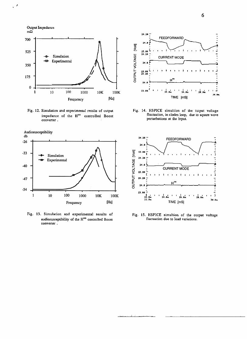
IV. RESUL TS AND DISCUSSION
Typical simulation results are depicted in Fig.IO-II. They
point out the contrast between the H~ controller andtraditional controllers. The H~ control exhibits a widerbandwidth for both output impedance and audiosusceptibility.This is obtained at the expense of the inferior performance of
the H~ controller at DC. It should be pointed out that thepeak with the H~ control at high frequency (Fig. 10 and II)is due to the limited bandwidth of the LM324. These peakdisappear if ideal operational amplifiers are used in thesimulations.
The experimental results for the H~ case were found tobe in good agreement with the simulation results (Figs. 12-13). The apparent discrepancy of the audiosusceptibility dataat low frequency (Fig. 13), may have been due to groundloops interferences.
The performance of the H~ controlled signal to largesignal perturbations was studied by simulation (Figs. 14,15).The simulation runs clearly point to the wider bandwidth ofthe H~ controller as compared to the feedforward and currentmode controller It thus appears that except for the low DCgain, the H~ potentially superior to classical controlmethods.
Fig. 11. Audiosusceptibility (in dB) of the Boostconverter under the four control schemes(simulation results).
REFERENCES
[1] Unitrode, Switching Regulated Power Supply DesignSeminar Manual. Unitrode Corporation. 1986.
[2] J.C. Doyle, K. Glover, P.P. Khargonekar and B.A. Francis,
"State space solution to tandard H2 and Hoo controlproblems," IEEE Trans. Automatic Control, vol. AC-34, no.8, pp. 831-847, 1989.
Output Impedancem .0. ZO\Jt
1ee.e..:- Voltage ModeI .( ::
6ee.e..:- ii: ~
5ee e.. -; ; /.-1 !
I \4ee.em- : ;
-I...
-.~. ..
~ ~ ... t 3ee.e..- / ...: :.
-I ...:
I .....
2ee .e.. :- I Current Mode;! :.;.I.' I
I ,/lee.em- .; .1 ..-, ...
...: " Feedforward
e ' ., ., ",,1 ",1 ., , , "." ,,1 , ...",,1 ., 1.le.e lee.e 1.ei< 1e.ei< 1ee.ei<1.e hertz (109) 1.e
Frequency [Hz]
[3] B.A. Francis, A Course in H~ Control Theory, Springer-Verlag, New York, 1987.
[4] K.K. Sum, Switch Mode Power Conversion, Marcel1 Dekker,New York, 1989.
[5] S. Ben- Yaakov, "SPICE simulation of PWM DC-DCconverter systems: voltagefeedback, continuous inductorconduction mode," IEEE Electronics Letters,vol. 25, no.16,pp. 1061-1062, 1989.
Fig. 10. Output impedance of the Boost converter underthe four control schemes (simulation results).
~~
6
Output ImpedancemQ
I I I I
-&- Simulation
-9- Experimental
!I -
===--""
10 100 1000 10K looK
Frequency [Hz]
TIME [mS] 3e.e..1
Fig. 14. HSPICE simultion of the tutput voltagefluctuation, in clodes loop, due to square waveperturbations at the input.
Fig. 12. Simulation and experimental results of output
impedance of the Hoo controlled Boostconverter .
3e.8..22.8.. TIME [mS]
Fig. 13. Simulation and experimental results of
audiosusceptibility of the Roo controlled Boostconverter .
Fig. 15. HSPICE simultion of the output voltagefluctuation due to load variations.
,,~
24.28 -
: FEEDFORWARD :
= 2 4 .e
r --V! ~-
o --
> --
~23.8eL".I,.,I...I..,-W 24.2e -
~ CURRENT MODE
~ 24 .e L--~ f-~ .:O ~ ' ...~- ~
>
1- 2'.8e i.. I I -'
~ 24.2e -
1-:) -~ -0 -H -
24.e ~." ". ~
238 .r II III, '-'.D 24.e.. 26 28.e..