Embed Size (px)
Citation preview
R. B. Darling / EE-527 / Winter 2013
EE-527: MicroFabrication
Oxidation of Silicon
R. B. Darling / EE-527 / Winter 2013
Silicon Dioxide (SiO2)
• The single thermodynamically stable oxide of silicon. • Essential to the fabrication of MOS devices.
– Creates extremely high electronic quality gate oxides.
• Essential to the patterning of silicon for high temperature processing. – Photoresist cannot handle temperatures much above 150C. – Patterned SiO2 can be used for masking diffusions, etches, and
other processes up to temperatures of >1400C.
• The extreme purity and perfection of the Si/SiO2 interface is the ultimate reason why silicon has been the #1 semiconductor for microelectronics. – And is likely to remain so…
R. B. Darling / EE-527 / Winter 2013
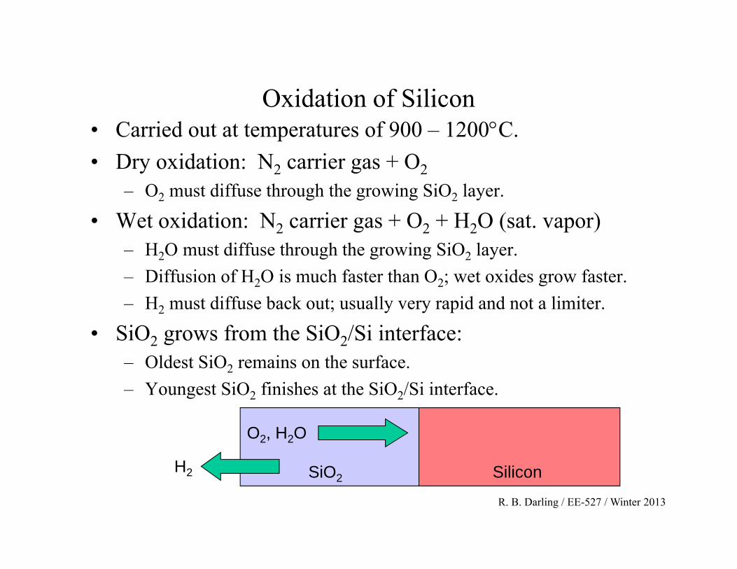
Oxidation of Silicon• Carried out at temperatures of 900 – 1200C. • Dry oxidation: N2 carrier gas + O2
– O2 must diffuse through the growing SiO2 layer.
• Wet oxidation: N2 carrier gas + O2 + H2O (sat. vapor)– H2O must diffuse through the growing SiO2 layer. – Diffusion of H2O is much faster than O2; wet oxides grow faster. – H2 must diffuse back out; usually very rapid and not a limiter.
• SiO2 grows from the SiO2/Si interface: – Oldest SiO2 remains on the surface. – Youngest SiO2 finishes at the SiO2/Si interface.
SiO2 Silicon
O2, H2O
H2
R. B. Darling / EE-527 / Winter 2013
Deal-Grove Model of Oxidation - 1
• B. E. Deal and A. S. Grove, J. Appl. Phys. 36, 3770 (1965). • A fairly simple and very descriptive model of silicon oxidation from a
gaseous source (O2, H2O), modeled after that for the oxidation of metal surfaces.
• Based upon the assumption of gaseous diffusion of the reacting species through a stagnant film adjacent to the growing oxide.
• Exhibits both transport-limited and reaction-rate-limited regimes.
R. B. Darling / EE-527 / Winter 2013
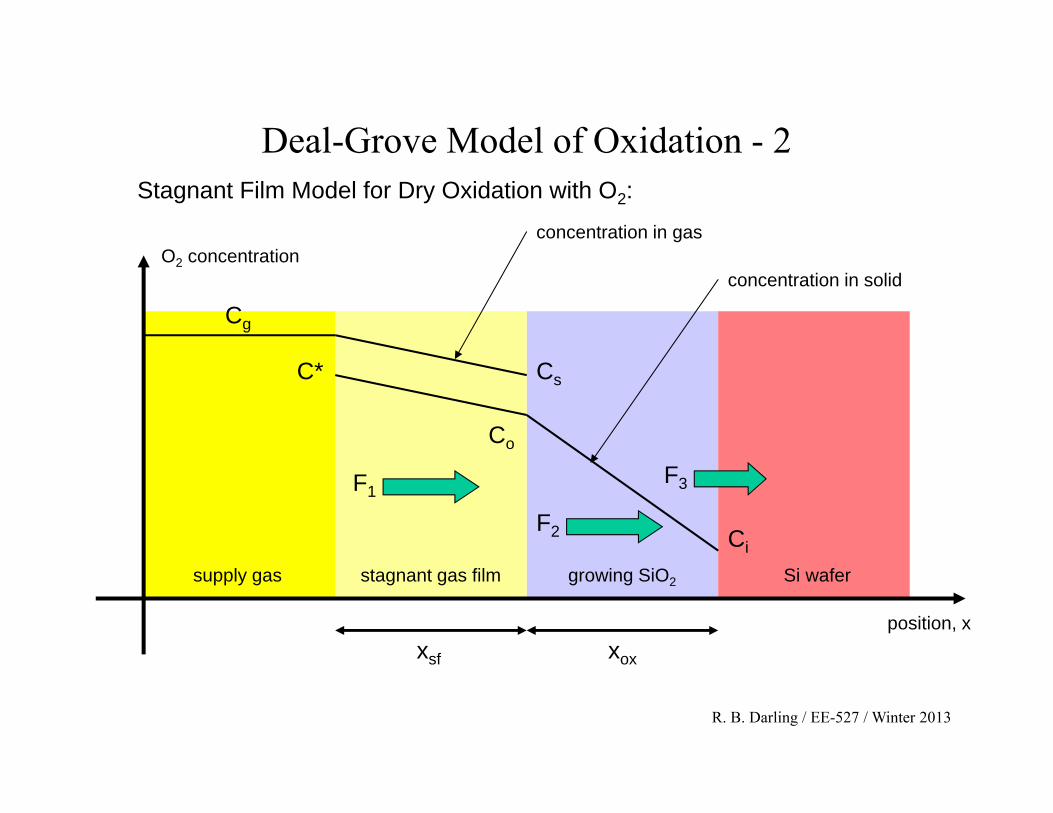
Deal-Grove Model of Oxidation - 2
supply gas stagnant gas film growing SiO2 Si wafer
O2 concentration
xsf xox
position, x
Cg
CsC*
Co
Ci
concentration in gas
concentration in solid
Stagnant Film Model for Dry Oxidation with O2:
F1
F2
F3
R. B. Darling / EE-527 / Winter 2013
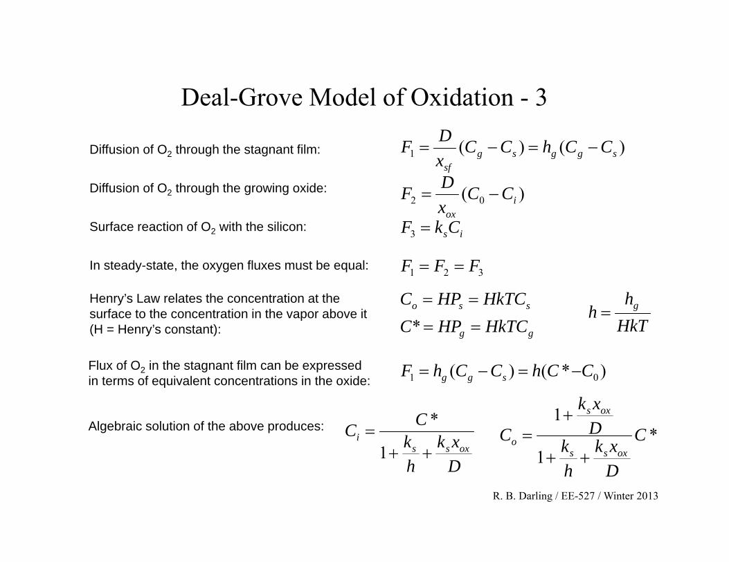
Deal-Grove Model of Oxidation - 3
)()(1 sggsgsf
CChCCxDF
)( 02 iox
CCxDF
isCkF 3
Diffusion of O2 through the stagnant film:
Diffusion of O2 through the growing oxide:
Surface reaction of O2 with the silicon:
In steady-state, the oxygen fluxes must be equal: 321 FFF
sso HkTCHPC
gg HkTCHPC *
)*()( 01 CChCChF sgg
Dxk
hk
CCoxss
i
1
**
1
1C
Dxk
hk
Dxk
Coxss
oxs
o
Henry’s Law relates the concentration at the surface to the concentration in the vapor above it (H = Henry’s constant):
Flux of O2 in the stagnant film can be expressed in terms of equivalent concentrations in the oxide:
Algebraic solution of the above produces:
HkTh
h g
R. B. Darling / EE-527 / Winter 2013
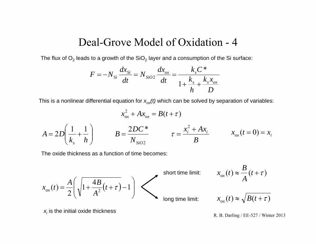
Deal-Grove Model of Oxidation - 4
Dxk
hk
Ckdt
dxNdt
dxNFoxss
soxSiO
SiSi
1
*2
)(2 tBAxx oxox
BAxx
NDCB
hkDA ii
SiOs
2
2
*2112
The flux of O2 leads to a growth of the SiO2 layer and a consumption of the Si surface:
This is a nonlinear differential equation for xox(t) which can be solved by separation of variables:
The oxide thickness as a function of time becomes:
141
2)( 2 t
ABAtxox
)()( tABtxox
)()( tBtxox
short time limit:
long time limit:
xi is the initial oxide thickness
iox xtx )0(
R. B. Darling / EE-527 / Winter 2013
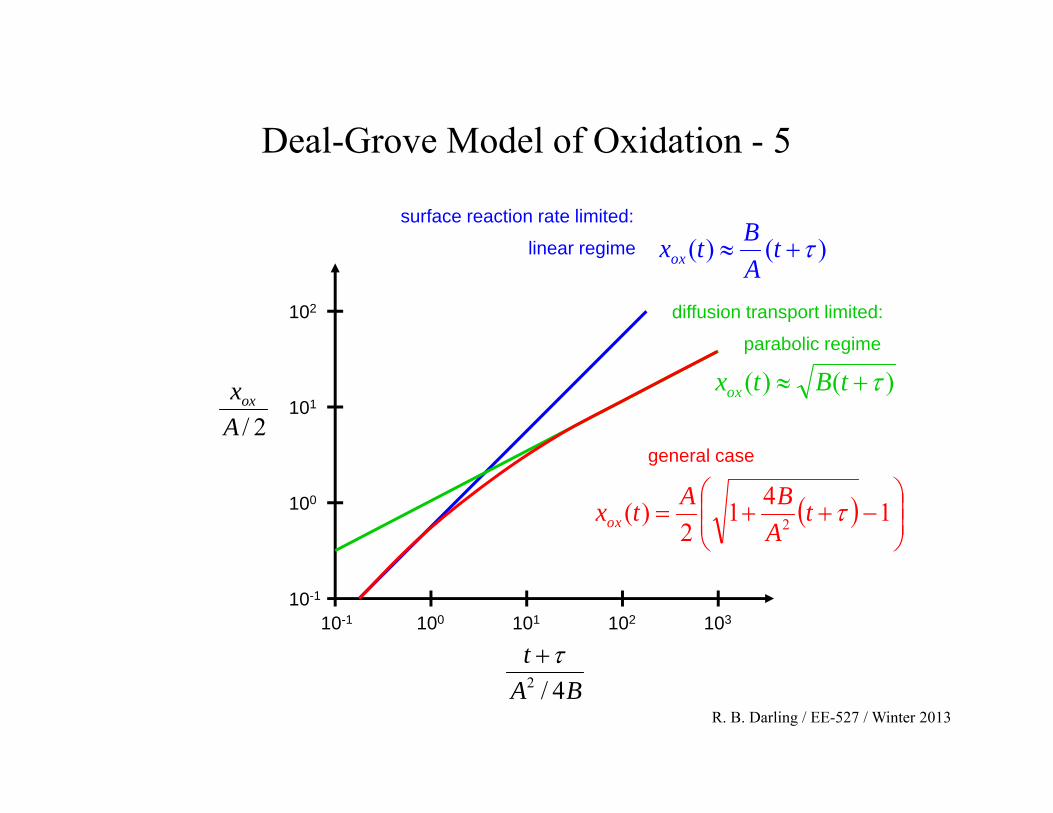
Deal-Grove Model of Oxidation - 5
10-1
100
101
102
10310210110010-1
)()( tABtxox
)()( tBtxox
141
2)( 2 t
ABAtxox
BAt
4/2
2/Axox
linear regime
parabolic regime
general case
surface reaction rate limited:
diffusion transport limited:
R. B. Darling / EE-527 / Winter 2013
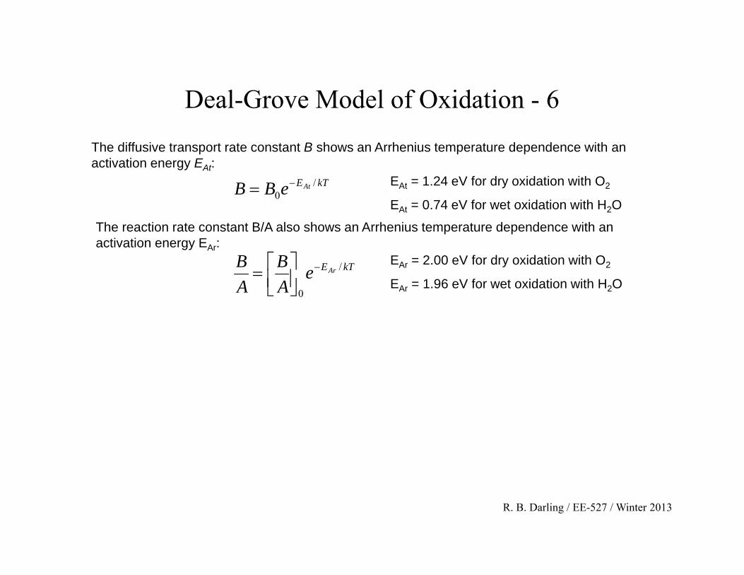
Deal-Grove Model of Oxidation - 6
kTEAteBB /0
kTEAreAB
AB /
0
The diffusive transport rate constant B shows an Arrhenius temperature dependence with an activation energy EAt:
EAt = 1.24 eV for dry oxidation with O2
EAt = 0.74 eV for wet oxidation with H2O
The reaction rate constant B/A also shows an Arrhenius temperature dependence with an activation energy EAr:
EAr = 2.00 eV for dry oxidation with O2
EAr = 1.96 eV for wet oxidation with H2O
R. B. Darling / EE-527 / Winter 2013
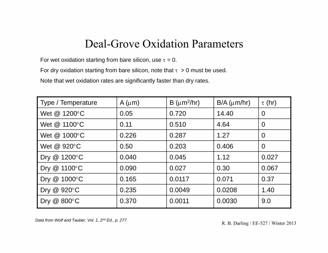
Deal-Grove Oxidation Parameters
Type / Temperature A (m) B (m2/hr) B/A (m/hr) (hr)Wet @ 1200C 0.05 0.720 14.40 0Wet @ 1100C 0.11 0.510 4.64 0Wet @ 1000C 0.226 0.287 1.27 0Wet @ 920C 0.50 0.203 0.406 0Dry @ 1200C 0.040 0.045 1.12 0.027Dry @ 1100C 0.090 0.027 0.30 0.067Dry @ 1000C 0.165 0.0117 0.071 0.37Dry @ 920C 0.235 0.0049 0.0208 1.40Dry @ 800C 0.370 0.0011 0.0030 9.0
Data from Wolf and Tauber, Vol. 1, 2nd Ed., p. 277.
For wet oxidation starting from bare silicon, use = 0.
For dry oxidation starting from bare silicon, note that > 0 must be used.
Note that wet oxidation rates are significantly faster than dry rates.
R. B. Darling / EE-527 / Winter 2013
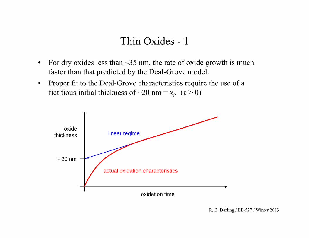
Thin Oxides - 1
• For dry oxides less than ~35 nm, the rate of oxide growth is much faster than that predicted by the Deal-Grove model.
• Proper fit to the Deal-Grove characteristics require the use of a fictitious initial thickness of ~20 nm = xi. ( > 0)
oxidation time
oxidethickness linear regime
actual oxidation characteristics
~ 20 nm
R. B. Darling / EE-527 / Winter 2013
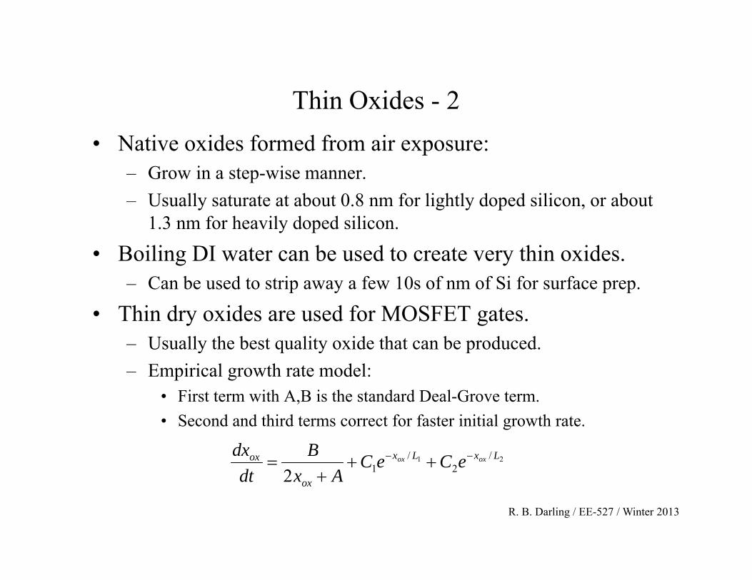
Thin Oxides - 2• Native oxides formed from air exposure:
– Grow in a step-wise manner. – Usually saturate at about 0.8 nm for lightly doped silicon, or about
1.3 nm for heavily doped silicon.
• Boiling DI water can be used to create very thin oxides. – Can be used to strip away a few 10s of nm of Si for surface prep.
• Thin dry oxides are used for MOSFET gates. – Usually the best quality oxide that can be produced. – Empirical growth rate model:
• First term with A,B is the standard Deal-Grove term. • Second and third terms correct for faster initial growth rate.
21 /2
/12
LxLx
ox
ox oxox eCeCAx
Bdt
dx
R. B. Darling / EE-527 / Winter 2013
Thin Oxides - 3
• Modern MOSFETs require gate oxides with thicknesses of only 2-5 nm! (usually called ultra-thin oxides)
• Controllable growth of oxides this thin requires: – Reduced temperature growth– Reduced pressure growth– Rapid thermal oxidation (RTO)
• Pure O2 at 1 atm• ~1050C for 40 seconds, via quartz lamps
R. B. Darling / EE-527 / Winter 2013
Use of Chlorine
• Increases the oxidation rate. • Improves the oxide quality:
– Reduced mobile ionic charge (Na+ gettering)– Increased minority carrier lifetime in underlying silicon– Increased oxide breakdown voltage– Reduced interface and fixed charge density– Reduced oxidation-induced stacking faults
• Chlorine sources: – Chlorine gas, Cl2
– Hydrogen chloride, HCl– Trichloroethylene, TCE, Cl3CCH– 1,1,1-Trichloroethane, TCA, Cl3CCH3
– Trans-1,2-Dichloroethane, DCE, Cl2CCH2
– Oxalyl Chloride, OC, Cl2C2O2
R. B. Darling / EE-527 / Winter 2013
High Pressure Oxidation (HIPOX)
• Approximately linear dependence of Deal-Grove B and B/A rate coefficients with oxygen pressure.
• HIPOX systems usually operate at PO2 ~ 10-25 atm. • Approximately, each atm of pressure is equivalent to 30C in
temperature to keep the oxide growth rate constant. • Usually needed to grow oxides thicker than 1.5-2.0 microns in a
reasonable period of time. – Thick field oxides
• Gasonics is one well-known vendor for HIPOX systems.
R. B. Darling / EE-527 / Winter 2013
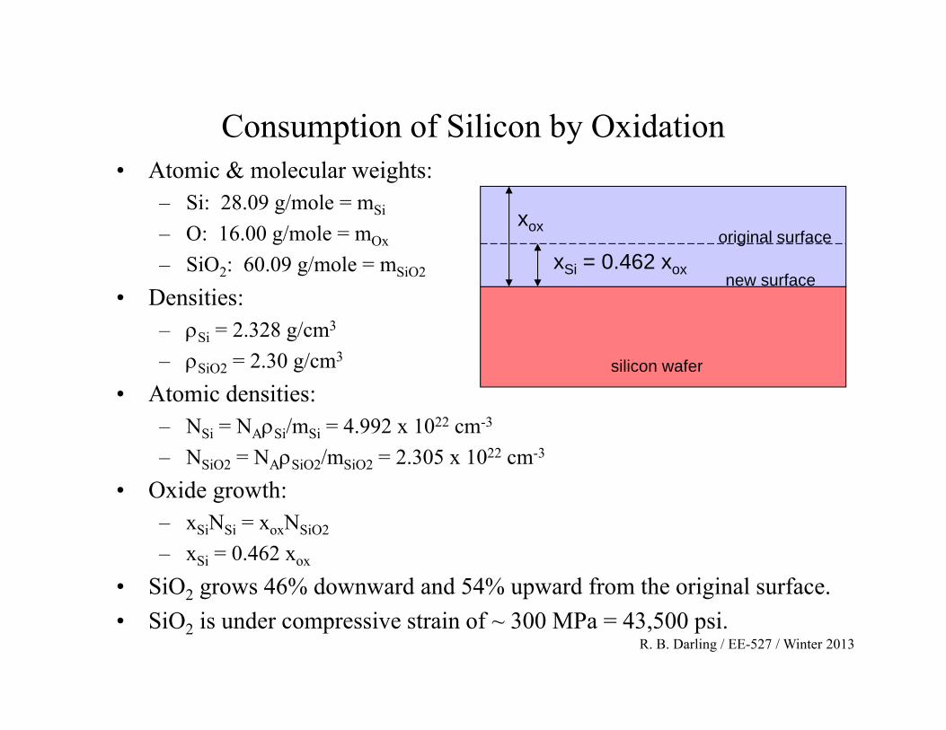
Consumption of Silicon by Oxidation• Atomic & molecular weights:
– Si: 28.09 g/mole = mSi
– O: 16.00 g/mole = mOx
– SiO2: 60.09 g/mole = mSiO2
• Densities: – Si = 2.328 g/cm3
– SiO2 = 2.30 g/cm3
• Atomic densities: – NSi = NASi/mSi = 4.992 x 1022 cm-3
– NSiO2 = NASiO2/mSiO2 = 2.305 x 1022 cm-3
• Oxide growth: – xSiNSi = xoxNSiO2
– xSi = 0.462 xox
• SiO2 grows 46% downward and 54% upward from the original surface.• SiO2 is under compressive strain of ~ 300 MPa = 43,500 psi.
xox
xSi = 0.462 xox
silicon wafer
new surface
original surface
R. B. Darling / EE-527 / Winter 2013
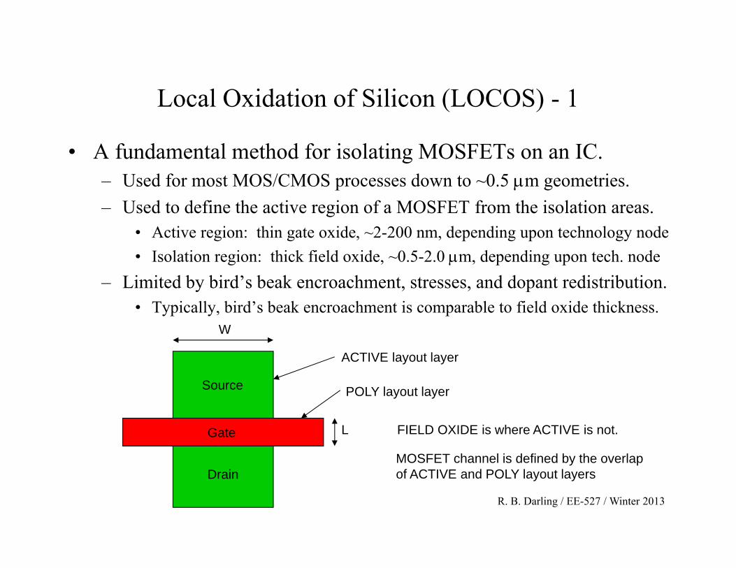
Local Oxidation of Silicon (LOCOS) - 1
• A fundamental method for isolating MOSFETs on an IC. – Used for most MOS/CMOS processes down to ~0.5 m geometries. – Used to define the active region of a MOSFET from the isolation areas.
• Active region: thin gate oxide, ~2-200 nm, depending upon technology node• Isolation region: thick field oxide, ~0.5-2.0 m, depending upon tech. node
– Limited by bird’s beak encroachment, stresses, and dopant redistribution. • Typically, bird’s beak encroachment is comparable to field oxide thickness.
L
W
ACTIVE layout layer
POLY layout layer
FIELD OXIDE is where ACTIVE is not.
MOSFET channel is defined by the overlapof ACTIVE and POLY layout layers
Source
Gate
Drain
R. B. Darling / EE-527 / Winter 2013
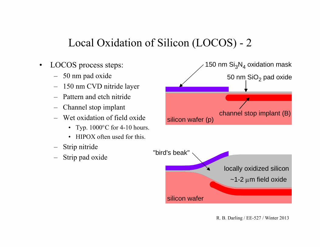
Local Oxidation of Silicon (LOCOS) - 2
• LOCOS process steps: – 50 nm pad oxide– 150 nm CVD nitride layer– Pattern and etch nitride– Channel stop implant– Wet oxidation of field oxide
• Typ. 1000C for 4-10 hours. • HIPOX often used for this.
– Strip nitride– Strip pad oxide
150 nm Si3N4 oxidation mask
50 nm SiO2 pad oxide
silicon wafer (p)
"bird's beak"
silicon wafer
locally oxidized silicon~1-2 m field oxide
channel stop implant (B)
R. B. Darling / EE-527 / Winter 2013
Shallow Trench Isolation (STI) - 1
• Key features: – Silicon trench is etched around active areas for MOSFETs, – Deposited dielectric is backfilled into trenches, and – CMP is used to planarize the result.
• Used for nearly all submicron MOS processes (L < 0.35 m)– Eliminates the bird’s beak encroachment of LOCOS. – Supports the use of implants for retrograde wells. – Channel stop implants not needed for sufficiently deep trenches. – Reduced mechanical stress from LOCOS nitride bending. – Reduced channel stop dopant redistribution.
R. B. Darling / EE-527 / Winter 2013
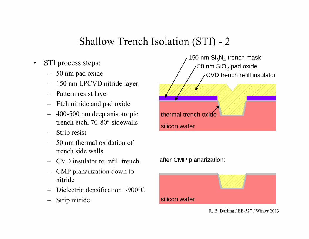
Shallow Trench Isolation (STI) - 2
• STI process steps: – 50 nm pad oxide– 150 nm LPCVD nitride layer– Pattern resist layer– Etch nitride and pad oxide– 400-500 nm deep anisotropic
trench etch, 70-80 sidewalls– Strip resist– 50 nm thermal oxidation of
trench side walls– CVD insulator to refill trench– CMP planarization down to
nitride– Dielectric densification ~900C– Strip nitride
silicon wafer
silicon wafer
150 nm Si3N4 trench mask50 nm SiO2 pad oxide
CVD trench refill insulator
after CMP planarization:
thermal trench oxide
R. B. Darling / EE-527 / Winter 2013
Crystallographic Orientation Effects
• Most oxide growth rates are quoted for the (100) planes of Si, which is most common for microelectronics processing.
• Surface reaction rate depends upon the density of Si atoms on a given surface and the orientation of the bond angles to that surface.
• (111)Si has a greater density of atoms than (100)Si. – This is a subtle point, often argued, and ends up depending upon which
plane is chosen to cut through the crystal. – Note that the average surface density of Si atoms is the same for all
orientations. • (111)Si has perpendicular surface bonds, while (100)Si has surface
bond angles that are oblique to the surface (~54 from normal). • Experimentally, the B/A rate constant is found to be a factor of 1.65 –
1.75 larger for the (111) planes over the (100) planes. • This is responsible for the “corner-pinch” effect observed for where
(111) planes meet (100) planes in an etched pit.
R. B. Darling / EE-527 / Winter 2013
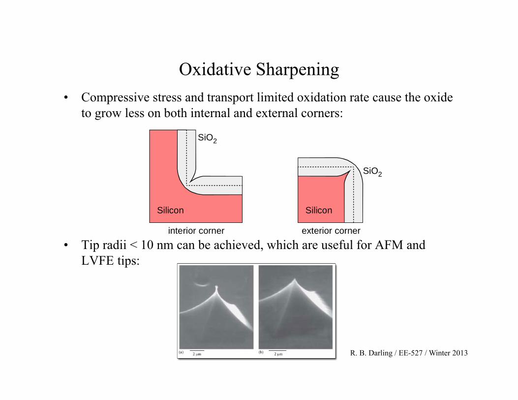
Oxidative Sharpening• Compressive stress and transport limited oxidation rate cause the oxide
to grow less on both internal and external corners:
• Tip radii < 10 nm can be achieved, which are useful for AFM and LVFE tips:
Silicon Silicon
interior corner exterior corner
SiO2
SiO2
R. B. Darling / EE-527 / Winter 2013
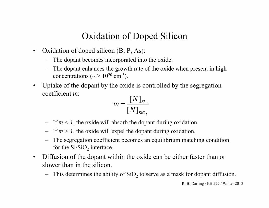
Oxidation of Doped Silicon• Oxidation of doped silicon (B, P, As):
– The dopant becomes incorporated into the oxide. – The dopant enhances the growth rate of the oxide when present in high
concentrations (~ > 1020 cm-3). • Uptake of the dopant by the oxide is controlled by the segregation
coefficient m:
– If m < 1, the oxide will absorb the dopant during oxidation. – If m > 1, the oxide will expel the dopant during oxidation. – The segregation coefficient becomes an equilibrium matching condition
for the Si/SiO2 interface. • Diffusion of the dopant within the oxide can be either faster than or
slower than in the silicon. – This determines the ability of SiO2 to serve as a mask for dopant diffusion.
2][][
SiO
Si
NNm
R. B. Darling / EE-527 / Winter 2013
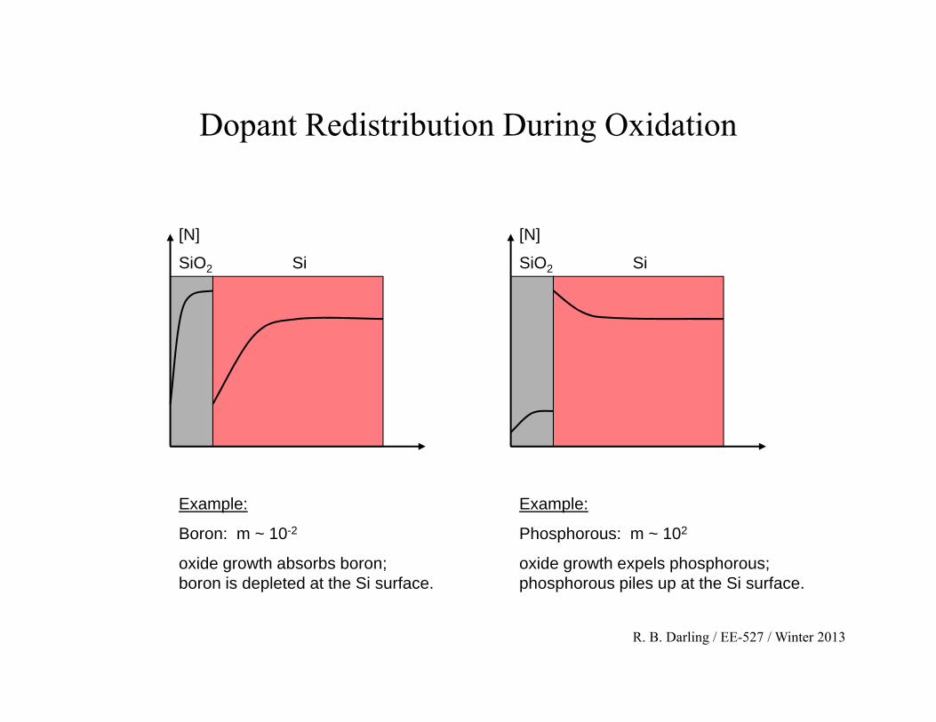
Dopant Redistribution During Oxidation
SiO2 Si
[N]
Example:
Boron: m ~ 10-2
oxide growth absorbs boron;boron is depleted at the Si surface.
SiO2 Si
[N]
Example:
Phosphorous: m ~ 102
oxide growth expels phosphorous;phosphorous piles up at the Si surface.
R. B. Darling / EE-527 / Winter 2013
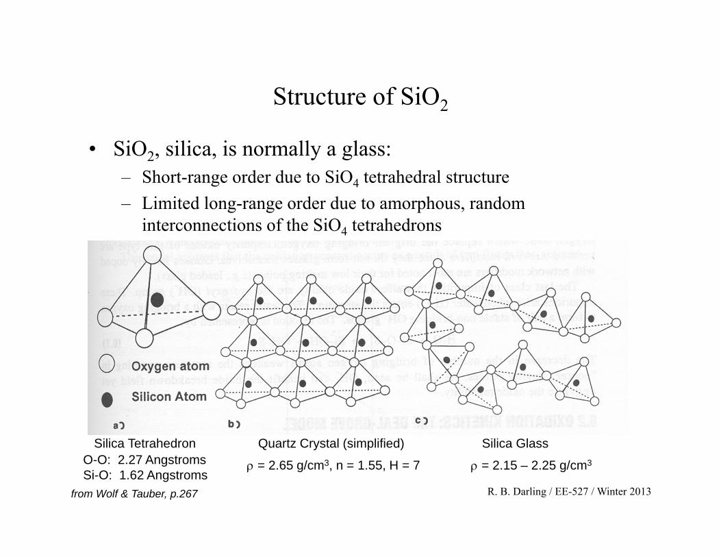
Structure of SiO2
• SiO2, silica, is normally a glass: – Short-range order due to SiO4 tetrahedral structure– Limited long-range order due to amorphous, random
interconnections of the SiO4 tetrahedrons
from Wolf & Tauber, p.267
Silica Tetrahedron Quartz Crystal (simplified) Silica Glass
= 2.65 g/cm3, n = 1.55, H = 7 = 2.15 – 2.25 g/cm3O-O: 2.27 AngstromsSi-O: 1.62 Angstroms
R. B. Darling / EE-527 / Winter 2013
Silica Glass
• Unit building block is the silica tetrahedron: [SiO4]4-
• Two silica tetrahedrons are connected by sharing an apical oxygen that forms a bridge between the two tetrahedra.
• If each tetrahedron is bridged to 4 other tetrahedrons, the system becomes charge neutral, and the overall chemical formula becomes SiO2.
• Non-bridging oxygens (NBOs) carry a −1 charge and will collect around unbound cation impurities.
R. B. Darling / EE-527 / Winter 2013
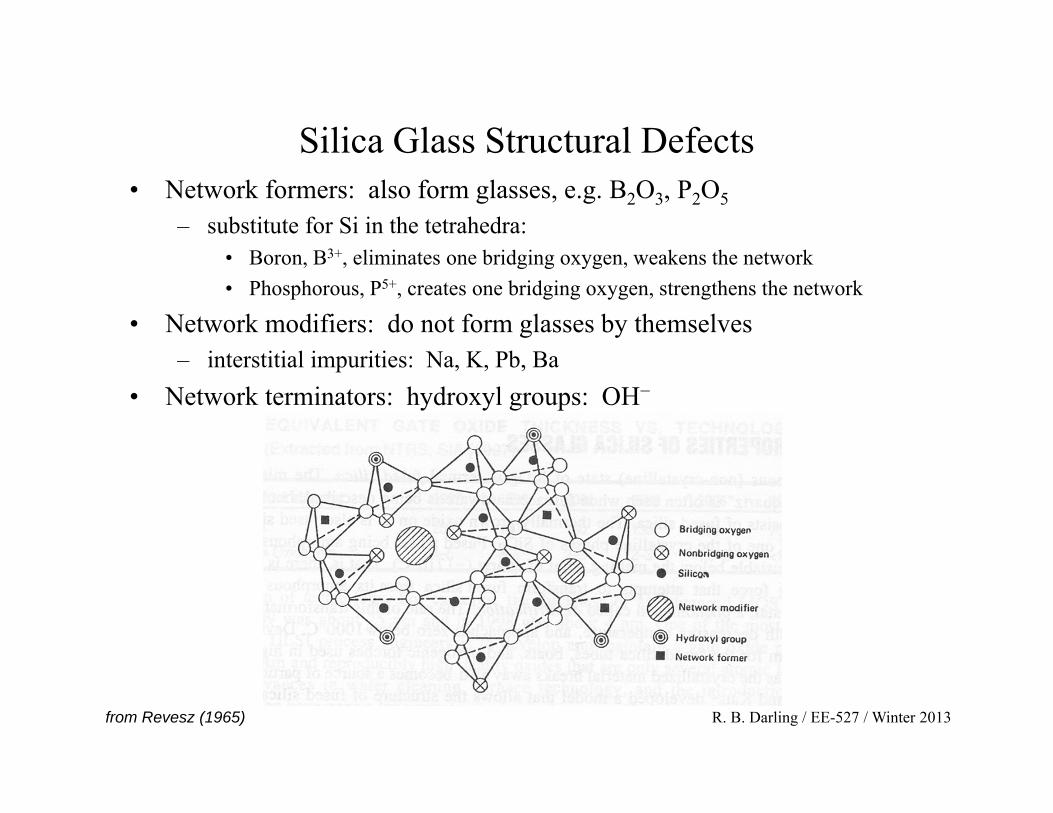
Silica Glass Structural Defects• Network formers: also form glasses, e.g. B2O3, P2O5
– substitute for Si in the tetrahedra: • Boron, B3+, eliminates one bridging oxygen, weakens the network• Phosphorous, P5+, creates one bridging oxygen, strengthens the network
• Network modifiers: do not form glasses by themselves– interstitial impurities: Na, K, Pb, Ba
• Network terminators: hydroxyl groups: OH−
from Revesz (1965)
R. B. Darling / EE-527 / Winter 2013
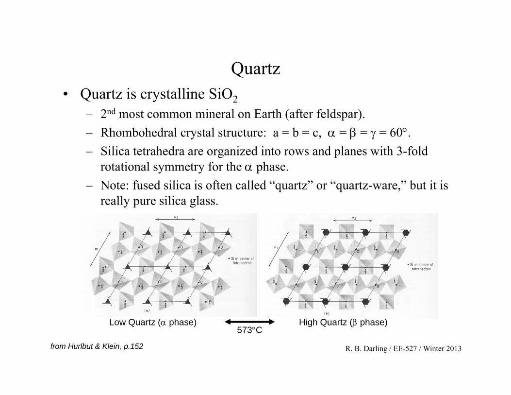
Quartz• Quartz is crystalline SiO2
– 2nd most common mineral on Earth (after feldspar). – Rhombohedral crystal structure: a = b = c, = = = 60. – Silica tetrahedra are organized into rows and planes with 3-fold
rotational symmetry for the phase. – Note: fused silica is often called “quartz” or “quartz-ware,” but it is
really pure silica glass.
Low Quartz ( phase) High Quartz ( phase)573C
from Hurlbut & Klein, p.152
R. B. Darling / EE-527 / Winter 2013
Low Temperature Glasses
• Examples: – LTO = Low Temperature Oxide– PSG = Phospho-Silicate Glass– BSG = Boro-Silicate Glass– BPSG = Boro-Phospho-Silicate Glass
• All are deposited by CVD or LPCVD processes. • Are used extensively for inter-level dielectrics in back-end
processing. • Low temperature refers to a low glass transition
temperature which allows the deposited glass to be reflowed and densified at temperatures which are compatible with the interconnect metals, usually < 400C.
R. B. Darling / EE-527 / Winter 2013
Spin-On Glasses (SOG)• Used for inter-level dielectrics in back-end processing. • Usually have viscosities and wetting characteristics which allow them
to fill in recesses and flow away from high spots, providing a degree of planarization for the next metal layer.
• Based upon organic-siloxane compounds: – Methyl siloxane polymers– Ethyl siloxane polymers
• Can be easily applied by spin-coating to thicknesses in the range of 50 to 300 nm. Thicker films can be obtained through multiple coats.
• Resulting SiO2 layer after curing is of lower quality than that of a thermally grown oxide: – More porous, less dense, lower refractive index. – Higher etch rates in HF and BOE. – Too many surface states and trapped charge to be useful as a MOS
insulator. – Lower breakdown voltage.
R. B. Darling / EE-527 / Winter 2013
Spin-On Glass Curing Schedule• The concept is to spin cast the film, evaporate off any coating solvent,
polymerize the siloxanes, and then decompose and evaporate the carrier organics.
• Typical curing schedule: – 80C for 1 minute on a hotplate. – 250C for 1 minute on a hotplate. – 425C for 2 hours in a box furnace with 5-10 SCFH of N2 cover gas.
• While the electrical characteristics of a SOG film are not the best, the ease of application makes it attractive for many instances where a thin film insulator is required.
• SOG films are also particularly useful as dopant sources. – Boron and phosphorous SOG sources are available. – They offer much simpler and safer alternatives to gas source or solid
source dopants. – Process recipes usually have to be adjusted to accommodate them.
R. B. Darling / EE-527 / Winter 2013
Oxides of Other Semiconductors
• Germanium– GeO, GeO2:
• Unstable at high temperatures• Water soluble!
• Gallium Arsenide– GaO, Ga2O3, GaO2, As2O3, AsO2:
• A mixture of several oxides with differing properties• Unstable at high temperatures• Oxide grows backwards:
– As and Ga are more volatile than O2, so they diffuse out through the growing oxide, rather than O2 diffusing in.
– Oxide is loosely attached to the GaAs surface; it can often be shaken or rubbed off.
• Si and SiO2 are very unique and ideal for microelectronics!
R. B. Darling / EE-527 / Winter 2013
Oxides of Metal Surfaces• Oxidation of some metal surfaces also follows the Deal-Grove model: • Alumina:
– 4Al + 3O2 → 2Al2O3
• Titania: – Ti + O2 → TiO2
• Iron (III) oxide (ferric): (hematite)– 4Fe + 3O2 → 2Fe2O3
• Iron (II) oxide (ferrous): – 2Fe + O2 → 2FeO
• Iron (II,III) oxide: (magnetite)– 3Fe + 2O2 → Fe3O4
• Copper (II) oxide (cupric) (black)– 2Cu + O2 → 2CuO2
• Copper (I) oxide (cuprous) (red) (a semiconductor!)– 4Cu + O2 → 2Cu2O
Because the oxidation process involves the diffusion of oxygen through the growing oxide layer, the process becomes self-limiting and the oxidation passivates the metal surface.
The red, gelatinous rust of iron or steel is a hydrated form of ferric oxide, Fe2O3·H2O.