Embed Size (px)
Citation preview

Vol. 105, No. 4, April 2017 | Proceedings of the IEEE 593
Manuscript received June 17, 2016; revised September 12, 2016; accepted October 31, 2016. Date of publication January 2, 2017; date of current version March 20 2017.F. Calignano, D. Manfredi and E. P. Ambrosio are with the Istituto Italiano di Tecnologia, Center for Sustainable Futures - CSF@PoliTo, Turin 10129, Italy (e-mail: [email protected]).S. Biamino, M. Lombardi and P. Fino are with the Dipartimento di Scienza Applicata e Tecnologia, Politecnico di Torino, Turin 10129, Italy.E. Atzeni, A. Salmi, P. Minetola and L. Iuliano are with the Dipartimento di Ingegneria Gestionale e della Produzione, Politecnico di Torino, Turin 10129, Italy.
Digital Object Identifier: 10.1109/JPROC.2016.2625098
Overview on Additive Manufacturing TechnologiesThis paper presents an overview of the main additive manufacturing/3-D-printing technologies that are suitable for many satellite applications, and in particular RF components. These technologies represent potential solutions for low-volume manufacturing of high value and highly complex parts and products.
By Fl av i a na Ca l igna no, Diego Ma nFr eDi, el isa Paol a a MBrosio, sa r a Bi a Mino,Ma r i a ngel a loMBa r Di, el eonor a atzeni, a l essa nDro sa l Mi, Paolo Minetol a,luC a iu l i a no, a nD Paolo Fino
ABSTRACT | This paper provides an overview on the main
additive manufacturing/3D printing technologies suitable for
many satellite applications and, in particular, radio-frequency
components. In fact, nowadays they have become capable of
producing complex net-shaped or nearly net-shaped parts in
materials that can be directly used as functional parts, including
polymers, metals, ceramics, and composites. These technologies
represent the solution for low-volume, high-value, and highly
complex parts and products.
KEYWORDS | 3D printing; additive manufacturing (AM);
electron beam melting (EBM); fused deposition modeling (FDM);
material jetting; power-bed fusion; selective laser melting (SLM);
stereolitography (SL); vat photo-polymerization
I . IN TRODUCTION
Developed in the 1980s, additive manufacturing (AM), known as Rapid Prototyping [1], is defined by the American Society of Testing and Materials (ASTM) as “ The process of joining materi-als to make objects from 3D model data, usually layer upon layer, as opposed to subtractive manufacturing methodologies; Syno-nyms: 3D printing, additive fabrication, additive process, additive techniques, additive layer manufacturing, layer manufacturing, and
freeform fabrication.” [2] According to the ASTM, the range of AM technologies is classified into several categories (Table I): binder jetting, material jetting, direct energy deposition, sheet laminations, material extrusion, powder bed fusion, and vat photo-polymerization [2], [3]. Each category includes several distinct processes, but alzl of them share the principle used for the selective modelling of the layers. The parts produced by AM technologies have some anisotropy in a particular direction due
0018-9219 © 2017 IEEE. Personal use is permitted, but republication/redistribution requires IEEE permission. See http://www.ieee.org/publications standards/publications/rights/index.html for more information.
Table I Astm classifications (2012) [2]

Calignano et al . : Overview on Additive Manufacturing Technologies
594 Proceedings of the IEEE | Vol. 105, No. 4, April 2017
to stacking layers. Anisotropy can be reduced by selecting the appropriate orientation during the manufacturing of the part.
In terms of materials, a diversity of polymers, ceramics, metals, and composites can be used for AM. The use of these materials is conditioned on the type of AM process used [4].
The first applications of AM were in the area of rapid proto-typing and then tooling. These application areas continue to be exploited, but the growing performances of AM technologies have expanded the fields and are thus increasingly used for the direct production. Industries such as aerospace, in which the need to produce highly complex aircraft components makes the application of AM technologies ideal, are already fully aware of their potential and are investing in research to improve their reliability and applicability [4], [5]. In the medical sector, appli-cations highly personalized in orthodontics, prosthetics, orthot-ics, implants, and replacement organs produced by AM process are already at a certain level of maturity and use [6]. In recent years, there have been applications of AM technologies also in the radio-frequency (RF) field to develop a next-generation of microwave and millimeter-wave devices aimed at several appli-cations operating from few to hundreds of gigahertz, among which are millimeter-wave wireless communications systems for gigabit wireless local area networks, wearable sensors, auto-motive collision avoidance, high-resolution imaging systems, and satellite communication, and RF MEMS devices [7–12].
AM and traditional manufacturing face off the trade-offs in the deployment of productive capabilities. AM has the potential to reduce waste, reduce lead time and cost, and to design products with complex parts. In addition, the AM allows building objects that are assembled by reducing the overheads associated with documentation and production planning [13]. Furthermore, by eliminating tools, the design of parts can be realized with the same specifications of the parts made with traditional technologies but with less mate-rial. Additive techniques enable rapid response to markets as the possibility to produce on demand the spare parts, reducing or eliminating the need for stockpiles.
This paper reviews the AM techniques suitable for many satellite applications and, in particular, RF components.
II . A DDITI V E M A N U FACT U R ING TECHNOLOGIES
Currently, the techniques mostly investigated for satellite applications are material extrusion, material jetting, vat photopolymerization, and powder-bed fusion.
A. Material Extrusion
The process of fused deposition modelling (FDM TM ) consists in the extrusion and subsequent deposition of a molten filament of polymeric material. It was invented by Scott Crump and patented in 1989. Crump together with his wife Lisa founded the company Stratasys Inc., which is the worldwide leader for the FDM technology and top manufac-turer of industrial FDM systems.
After the expiration of Crump’s patent, the diffusion of FDM technology was boosted by the development of a wide variety of low-cost FDM machines. Nowadays these machines are popularly called 3D printers. Actually the term 3D print-ing is erroneously adopted for the FDM process, because the Three-Dimensional Printing technology (3DP TM ), originally developed at the Massachusetts Institute of Technology (MIT) in 1993, was marketed by Z Corp. 3DP is different from FDM, since it deposits a liquid binder onto thin layers of powder to create parts layer by layer (inkjet printing technology).
Recently, the ASTM International Technical Commit-tee F42 on Additive Manufacturing (AM) Technologies has released the F2792 document about Standard Terminology for AM Technologies to distinguish between the diverse processes and classify them according to standard terms. In the ASTM F2792, FDM is classified under the category of Material Extrusion processes, distinctly from 3DP that belongs to the Binder Jetting type.
In its physical principle, the FDM process is very similar to the one of the hot glue gun and relatively simple. A filament of polymeric material is softened and melted with the aid of heat and is extruded, i.e., pushed and forced through a noz-zle of reduced diameter and then deposited layer by layer on the building platform or bed [14]. The filament has a standard diameter of 1.75 mm or 3 mm and is supplied by spools. The most common FDM machine has a standard Cartesian struc-ture and an extrusion head. The filament is unrolled from the spool by means of a stepper motor and a set of gears, knurled pulleys, or screws that pinch and press the filament to push it through a guiding PTFE tube into the extrusion head. In some configurations, the filament feeding mechanism is not fixed on the machine case but is positioned just above the extru-sion head and moved with it. In the latter case, the filament is pulled along the PTFE guiding tube by the feeding mecha-nism and then pushed into the extrusion head (Fig. 1).
The extrusion head has up to three extruders. Each extruder has a chamber that is heated by means of electrical resistances, so the filament softens inside it and with a certain viscosity passes
Fig. 1. Scheme of the FDM process.

Calignano et al . : Overview on Additive Manufacturing Technologies
Vol. 105, No. 4, April 2017 | Proceedings of the IEEE 595
through the nozzle next to the chamber. The nozzle is inter-changeable and has an orifice of standard size, which ranges from 0.3 mm to 0.6 mm according to the machine or manufac-turer. The nozzle presses the extruded material on the building platform, so the gap between the nozzle and the bed corresponds to the thickness of the building layer. For this reason, setting the correct nozzle height and levelling the bed is very important.
The FDM machine is a computer numerical control (CNC) system governed by a main electronic board. The CNC unit controls the three Cartesian axes in speed and position through rotating speed and steps of stepper motors. With the control of the stepper motor of the feeding mechanism, the filament feed and extrusion conditions can be set, together with a closed-loop control of the temperature in the extruder chamber. Open source machines allow the user to edit the NC code that is writ-ten in ISO standard and contains the coordinates of the points for the trajectories of the extrusion head. The G1 code is used to define the point-to-point motion along straight lines, whereas M codes deal with other functions, such as the filament feed-ing, extruder heating, or the nozzle wiping.
Low-cost FDM machines are generally equipped with a sin-gle extruder, and the bed and working chamber are at room temperature. The machine setup is often manual in case of cali-bration operations or material change. Industrial FDM systems are equipped with a hot bed and hot working volume together with advanced mechatronics systems for improved position-ing accuracy and higher speed of motion of the extrusion head. The system setup is automatic, and the material change is fast because the filament is supplied in chipped cartridges. For most of the industrial FDM system, the NC code is not open and the job preparation is made by means of proprietary soft-ware. Industrial systems come with at least two extruders. One extruder is used to deposit the building material for the part; the other deploys a soluble material for supporting hollows shapes and overhanging surfaces. After fabrication, the support material is removed by drowning the build for some hours in a chemical bath that dissolves the supports.
The price of FDM machines starts from less than 1,000 € for self-assembly kits up to more than 200,000 € for an indus-trial system with a working volume of half of a cubic meter.
As concerns the materials (Fig. 2) available for the FDM process, the most commonly used ones are listed in the following.
• ABS (Acrylonitrile Butadiene Styrene) is the most com-mon thermoplastic used for making anything from musical instruments to automotive components. It can be recycled and prints on PET film with a light acetone/ABS top coat. ABS adheres well, so high printing speeds are possible. ABS is difficult because it tends to warp off the build platform when printing large parts. This can be remedied by using a heated bed. ABS filament is available in different colors.
• PLA(PolyActic Acid) is thermoplastic aliphatic poly-ester derived from renewable resources, like corn starches, so it is biodegradable and compostable. It is affordable and easy to use. PLA adheres to itself well, so high printing speeds are possible. It is dimension-ally stable, and it can be used without the need for a heated bed. It is harder than ABS, but it exhibits higher friction, thus it is more prone to extruder jams. However, this is more than compensated for its lower viscosity when molten. PLA is susceptible to heat and moisture and is not ideal as long-term out-door use or high temperature environments. When it is heated, the moisture absorbed from the air can turn to steam bubbles, which can interfere with cor-rect processing with certain extruder designs. Just as ABS, it comes in a good range of colors.
• HIPS (High Impact PolyStyrene) is a low-warp thermo-plastic filament. It is easy to paint and glue and one of the lightest FDM materials. It is available in a wide range of colors, and it is often used for preproduction prototypes because of its great dimensional stability. From the point of view of processing properties, it is very similar to ABS. However, the two materials work with different solvents: limonene for HIPS and acetone for ABS. So HIPS can be used as a support material due to limonene not affecting ABS. HIPS supports can be easily torn from the ABS, leaving an even finish behind.
• PC (PolyCarbonate) is a strong engineering polymer with high impact resistance for parts submitted to loads. It also has good temperature resistance. PC tends to warps significantly more than ABS or PLA, so the use of a heated bed is imperative. A heated bed of above 60 °C can overcome any problem of delamination. Moreo-ver, PC is very hygroscopic and absorbs moisture from the air, and this can cause problems during processing. PC comes in black, white, and clear colors.
• PA (PolyAmmide) is commercially and popularly renown as Nylon. Blends of different kind of polyam-ide with undisclosed contents and a wide variety of Fig. 2. FDM materials. Source: Stratasys [20].

Calignano et al . : Overview on Additive Manufacturing Technologies
596 Proceedings of the IEEE | Vol. 105, No. 4, April 2017
properties are available on the market. Prints are flexi-ble and wear-resistant. Unlike ABS and PLA, PA is less brittle and therefore stronger. PA has self-lubricating properties, which are useful for fabricating gears or nuts for screws. Being a semicrystalline thermoplas-tic, PA shrinks more than the other materials when it cools down after the deposition of each single layer. For this reason, it tends to warp more than ABS and PLA, and bed adhesion is more problematic. The use of a heated bed and heated building volume is advised.
Recently, some new technical polymers with improved performances were developed, such as:
• PVDF (PolyVinyliDene Fluoride) is characterized by an excellent resistance to creep and fatigue, radia-tion, and UV, an excellent thermal stability (being able to work between − 20 ° C and + 130 ° C ) and a high dielectric constant. In addition, thanks to its chemical stability, it is often employed as insulation and protection cover in chemical applications.
• PEEK (PolyEtherEtherKetone) is a high-performance semicrystalline thermoplastic able to show high strength and stiffness as well as high ductility. For these reasons, it can replace aluminium and steel in structural applications, offering reduced total weight and processing cycles. In addition, PEEK, being chemically resistant to aggressive environments, offers increased durability and possibility of steriliza-tion for medical and food contact applications.
• PEI (PolyEtherImide) is an amorphous, high-per-formance polymer with excellent thermal proper-ties, exceptional dimensional stability (low-creep sensitivity and low, uniform coefficient of thermal expansion), inherent flame retardancy, and good chemical resistance. In addition, PEI has consist-ent surface resistivity, long-term hydrolytic stability, high strength and modulus, even at elevated tem-peratures, good resistance to a broad range of chem-icals, such as automotive fluids, fully halogenated hydrocarbons, alcohols, and aqueous solutions, sta-ble dielectric constant, and dissipation factor over a wide range of temperatures and frequencies. Gener-ally, it presents characteristics similar to PEEK but with lower impact strength, usable temperature (it performs in continuous use up to 170 °C), and cost.
Process temperature for the above-listed materials is indicated in Table II. Those temperatures may vary depend-ing upon the specific material composition. The rule of thumb is that the higher the extrusion temperature, the lower the viscosity, i.e., the material flows more easily, and a higher deposition speed can be used.
The commercial price of FDM filaments is approxi-mately forty times that of the raw material. The ratio can be even higher for materials with specific composition (fiber reinforcement or fillers) or particular aesthetics properties (glossy, glowing, translucent).
Stratasys, which is the marked leader for industrial FDM systems, proposes a range of materials (Fig. 2) to cover dif-ferent applications (Table III). For some of these materials, anisotropy is indicated with respect to the building orienta-tion. Apart from commodity polymers, some engineering polymers are available, such as PPSU (polyphenylsulfone) or ULTEM, a polyetherimide that in the grade 9085 is certified for aerospace (Table III). Other engineering polymers are also available. For example, the Arevo [15] company sells three different filaments: a PAEK (Polyaryletherketone), a PEEK (Polyetheretherketone), and a PARA (Polyarylamide), even with ESD properties for electronic or aerospace applications.
Finally, the IGUS Company [16] developed a tribo- filament commercially named Iglidur TM , with a declared resistance to abrasion that is 50 times higher than that of common 3D printing materials.
The surface roughness of FDM parts is deeply affected by the layer height of the prototypes, depending also on the shape of the part and surface curvature with respect to the building orientation [17], [18]. This parameter could be main-tained at its lower value so that better roughness values are obtained, but this would take a great deal of time. Your ideal layer thickness will depend on your part and application. For example, thick layers are ideal for building large manufactur-ing and parts quickly when surface finish is not a priority.
The FDM process is one of the few additive manufac-turing technologies that enables the fabrication of multi-material parts in a unique build by using more than one extruder. The use of a soluble material for supports allows the manufacturing of integrated assemblies with parts hav-ing relative motion or live hinges, provided that the proper allowance and clearance are assigned to the mating parts in the computer-aided design (CAD) model [19].
As it concerns the process accuracy, the quality of the parts depends on the building orientation, on the layer thickness, and on the feature size [21-24]. In terms of ISO IT grades, smaller features and dimensions have generally
Table II Common processing temperature for different FDM materials

Calignano et al . : Overview on Additive Manufacturing Technologies
Vol. 105, No. 4, April 2017 | Proceedings of the IEEE 597
a worst dimensional accuracy (above IT13), whereas large features are dimensionally more accurate (below IT12) [25]. These results can vary according to the material and machine used and are affected by the adopted layer thick-ness and nozzle size.
FDM parts can be polished to improve the smoothness of the part surface, whether it is painted or metal plated. Unconventional finishing processes might also be employed to improve the superficial finishing [26-28]. A wide range of applications in different sectors are reported for the FDM technology in the literature [29-37], and the use of ceramics materials for FDM has also been investigated [38-40].
FDM has been recently addressed as the most promis-ing and sustainable additive technology for in-space manu-facturing applications [41-43]. The use of a solid filament is an advantage in a vacuum or microgravity environment, where powder beds or liquids cannot be used as raw materi-als. A first experiment was made on the International Space
Station with a sealed 3D printer to prevent outgassing in the environment of the space station [44]. Nonetheless, there are no studies about the lifetime and deterioration of poly-meric materials over time when exposed to orbital radiation.
B. Material Jetting
In the material jetting process, developed in 1984, the 3D models are created through the use of movable inkjet print heads that jet photopolymer onto a build platform (Fig. 3). The droplets are ejected selectively as one or more print heads move across the build area [13].
The drop-on-demand technique is usually used to eject the drop, which obtains a high accuracy in the positioning, low waste, small droplet size and wider availability of mate-rial. The material deposited is cured by using UV (ultravio-let) light. The model is produced layer by layer. Substances used in material jetting are typically materials having a vis-cous nature capable of forming the drops as photopolymers
Table III List of the Commercial Materials by Stratasys

Calignano et al . : Overview on Additive Manufacturing Technologies
598 Proceedings of the IEEE | Vol. 105, No. 4, April 2017
or wax-like materials. To facilitate jetting, materials must be heated to pass from the solid state to the liquid, trying to reduce the viscosity that otherwise would not allow the outflow of the jet. For this reason, it is common practices to use solvents or other low viscosity components in the fluid.
It is possible to deposit materials of different colors and hardness in the same part, thus creating components with different properties and characteristics. The process requires support structures for overhangs. The supports are usually built in a different material. Along with the selected model materials, a gel-like support material facilitates successful printing of complicated geometries. Support material can be removed using a sodium hydroxide solution or water jet.
The material-jetting printers can produce parts with res-olution on the order of 10- 30 μm , making the layers barely noticeable. The scientific literature shows that process vari-ables, such as print head speed, droplet velocity, and droplet frequency, may influence the quality of the deposition [45-52]. However, the photoactive compounds tend to exhibit high absorption loss for electromagnetic waves, making it less desirable for electromagnetic applications [53].
The postprocessing required is limited due to the high accuracy of the process, and the aesthetic and functional qualities of a part are determined during the printing stage.
The main commercial applications for inkjet printing remain in graphics, product marking, coding, and dating. In recent years, there has been considerable interest in techno-logical areas, such as aerospace and defense, architecture, commercial products, consumer products (Fig. 4), automo-tive, medical, entertainment, and sport.
Over the last decade, aerospace innovators have pushed 3D printing beyond the realm of prototyping into advanced tooling and production applications. Polymers were devel-oped to print parts commonplace on aircraft and spacecraft. By combining oral scanning, reverse engineering (RE), and 3D printing, it is possible to produce crowns, bridges, stone models, and a range of orthodontic appliances quickly and accurately. Sporting goods prototypes often require a com-bination of rigid and flexible materials, such as a helmet hard shell and padded interior, or a pair of ski goggles with
tinted lenses and rubber overmolding. Material jetting tech-nology can produce prototypes with multiple materials and colors in a single, automated build, so it is ideal for sporting goods designers.
C. Vat Photopolymerization
Vat photopolymerization is defined as “an additive manufacturing process in which liquid photopolymer in a vat is selectively cured by light-activated polymerization” (F42.91, ASTM Subcommittee, 2012). The most common vat photopolymerization process is the Stereolithography (SL). SL was the first commercial AM system, developed in 1884 by Charles Hull who then founded 3D System Corpo-ration in 1986 [54].
The input data in the SL process is the 3D CAD model of the part to be fabricated, converted into the STL file for-mat. Since SL is a liquid-based process, there is no structural support during the building phase. Thus, SL usually requires additional support structures. These structures are specified by the operator in the part preparation phase along with the positioning and orientation of the part in the building volume and other machine parameters settings. Then, the model is sliced to generate 2D sections from 0.025 mm to 0.5 mm thick, and this information is transferred to the SL machine to fabricate the part. It is important to note that basically SL can process a single material, and also support structures are made from the same material of the part. The basic principle of the SL process is the polymerization of a photosensitive resin. The SL process starts when the build-ing platform is lowered from the top of the polymer vat by a layer thickness (Fig. 5). Then, an ultraviolet laser is used to selectively cure the resin, converting it into a layer of solid material. Thereafter, the platform is lowered again and a new layer is built on the top of the previous one.
Fig. 3. Scheme of the material jetting process.
Fig. 4. Multimaterials in one print. Source: Stratasys [20].

Calignano et al . : Overview on Additive Manufacturing Technologies
Vol. 105, No. 4, April 2017 | Proceedings of the IEEE 599
Commonly, a blade is used to provide a smooth resin layer. The process is repeated until completion of the part [46]. When the process is completed, the platform is raised and removed from the machine. During post pro-cessing, the part is cleaned in a chemical bath to remove wet resin, supports are detached, and the part is placed into a UV oven to complete the curing. In general, in the SL process the layer boundaries are first created and then the internal areas are irradiated by hatching patterns. When the photopolymer is exposed to the UV light and solidifies, it shrinks. The volumetric shrinking of the irra-diated area induces compression stresses on previous lay-ers. As a consequence, part edges curl upwards and other distortions of the part can occur. Moreover, stresses also remain in the part as residual stresses. To avoid curl distortion and reduce internal stresses, 3D Systems has developed different scan patterns, such as Weave (1990), Star Weave (staggered hatch, alternating sequence, retracted hatch, 1991) and, as further improvement after the development of epoxy photopolymers, ACES (Accu-rate, Clear, Epoxy, solid parts, 1996). In the Star Weave pattern (Fig. 6), after the exposure of the contour, each scan line is retracted so that it is attached to only one bor-der; orthogonal scans are carried out along x and y axes, and scanning sequence for x and y axes is alternated from layer to layer; moreover, scan lines in alternate layers are staggered so that scan lines overlap gaps between scan lines of the previous layer. The basic idea of the ACE pat-tern is that of curing each layer by multiple scans. During the first scan, the penetration depth does not reach the previous layer and more material is cured. Subsequent scans then complete the bond to the previous layer. In such a way, a 98% of solidification is reached with mini-mum distortion [55].
Developed in the late 1960s, photopolymers were applied in several areas, such as coatings, dentistry, or microelectronics. In the 1980s, they were applied to the “rapid prototyping” sector. In 1989 and 1990, the first U.S. patents on SL resins were published.
At the beginning of the development of SL technology, low molecular weight resins, such as polyacrylate or epoxy macromers, were used. Parts produced using these mate-rials were primarily glassy, rigid, and brittle. To improve the mechanical behavior of SL parts, new epoxy-based and hybrid polymers (epoxides with some acrylate content) were introduced on the market. In this way, the quality of the built part was increased, because such materials are more insensi-tive to humidity and shrinkage [56]. Besides, there is also the possibility to fabricate pseudo-elastomeric objects by using a combination of specific resins with nonreactive diluents, such as N-methylpyrrolidone (NPM) or water [57]. Moreo-ver, it is also possible to create polymer-ceramic composite objects simply suspended ceramic particles, such as alumina or hydroxyapatite, in the SL resin [58-60]. Table IV lists the properties, process details, and typical application for some of the most common materials used in SL [61].
The main advantage of the SL process is its ability to fabricate parts with smooth surfaces and high level of accu-racy. The average superficial roughness ( R a ) is typically below 10 μm , and the accuracy ranges from 0.025 mm to 0.05 mm per 25.4 mm of part dimension. These values may
Fig. 5. Vat photopolymerization process.
Fig. 6. (a) Star Weave pattern, the red line identifies the contour, c is the distance of each scan line from the contour, hs is the hatch distance, and g is the gap between scan lines. (b) Scan lines overlap, d is the scan lines shift between layers.

Calignano et al . : Overview on Additive Manufacturing Technologies
600 Proceedings of the IEEE | Vol. 105, No. 4, April 2017
vary depending on build parameters, part geometry and size, part orientation, and postprocessing methods. The differ-ent SL machines have building volume from small to large (up to 1500 × 750 × 550 mm3). The SL process is relatively quick; however, it often requires support structures, which adversely affect the surface quality touched by them, and long and labor-intensive postprocessing operations. SL parts can be further processed by finishing operations to improve the aesthetic appearance. Thus, parts can be sanded to elim-inate the support marks and painted. Also the range of mate-rials is wide enough to meet the need of different users, from general purpose materials to materials for specific applica-tions. To overcome the limitations in mechanical properties of SL parts, a metallization process can be applied to the surfaces of the component. Thus, the strength of SL parts is enhanced, while maintaining a low weight, and functional parts are obtained [9], [62]. Microstereolithography (MSL)
has evolved from SL to fabricate small-size, high-resolution parts based on a light-induced polymerization of a liquid resin [63], [64]. Two basic approaches are used:
• Dynamic mask method systems. A liquid crystal mask is used to expose the layer surface in one step. The resolution is limited by pixel size and diffrac-tion effects.
• Scanning MSL systems. Similarly to SL, a laser spot is focused on the layer surface. To get a better resolution than SL, the spot size is reduced to a few micrometers (scanning MSL systems). Several opto-mechanical scanning solutions have been developed to maintain uniform characteristics of the laser spot and thus pro-duce micro-features with high resolution [65].
Multiple material stereolithography (MMSL) uses dif-ferent materials while building a piece. To do this, when
Table IV List of the most common materials used in SL.

Calignano et al . : Overview on Additive Manufacturing Technologies
Vol. 105, No. 4, April 2017 | Proceedings of the IEEE 601
the material has to be changed, all the resin is drained, and the new material is filled. A material build schedule is required [66].
SL technology is applied in many industries, including the aerospace sector, to produce functional components in a cost-effective and quick manner and the production of prototypes for automotive design verification and functional testing. Complex functional electronic and electromechani-cal systems can be produced by integrating additive AM technologies with systems able to 1) insert, by process inter-ruption, electronic components into cavities specifically designed in the AM structure; 2) dispense different mate-rials depending on the functionality (i.e., conductive inks [67]); and 3) embed electronic components within polymer substrates during fabrication [68].
MSL is used for the fabrication of microelectrome-chanical system (MEMS) components [61]. The biomedi-cal applications of SL are numerous. However, the SL technique is not yet extensively used in the medical field. 3D models can be built from medical imaging data (x-ray CT scanners or RMI) to give an understanding of the shape, orientation, relative location, and size of internal structures. The dimensional accuracy and surface qual-ity of SL models derived from x-ray tomography has been proven to be reliable enough to be used in applications such as diagnosis, surgical planning, design of customized implants, or teaching surgical anatomy and biomolecular structures [69-72]. The implantation of patient-specific devices has been also reported in literature; in tissue engi-neering, the development of biodegradable polymers has allowed the preparation of restorable scaffolds for tissue generation [56], [73].
The most widespread clinical application of SL in den-tistry has been in the fabrication of surgical templates to assist in dental implant planning and placement [74]. Other applications include the fabrication of clear plastic ortho-dontic treatment devices (aligners) and the production of maxillary/mandibular prosthesis [75].
Due to the evolution of SL toward microfabrication, this technique can be applied in the chemical engineering field for the production of microtransducers, micropumps in microfluidic applications, or micro heat-exchangers with internal channels dimensions of millimeters. Thanks to the high-resolution and smooth surface finish of SL parts, this AM technique is used in filmmaking to create solid objects from digital models for visual special effects and to fabri-cate characters and props in stop-motion films. In design application, SL is the tool used by the designer to fabricate conceptual prototypes to communicate ideas to manufactur-ers or to physically visualize parts characterized by intricate undercuts, small features, and overhangs with the aim to push the boundaries of the computer-aided design. SL tech-nology can be used for the production of functional end-user performance prototypes also in the field of packaging and sporting goods (protective athletic cups).
D. Selective Laser Melting
Selective Laser Melting (SLM) process (Fig. 7) has been developed by Dr. M. Fockele and Dr. D. Schwarze of F & S Stereolithographietechnik GmbH, with Dr. W. Meiners, Dr. K. Wissenbach, and Dr. G. Andres of Fraunhofer ILT to pro-duce metal components from metallic powders. It is a pow-der bed fusion process that uses high intensity laser as an energy source to melt the powder layer by layer in accord-ance with the computer-aided design (CAD) data.
The SLM process consists of a series of steps from CAD data preparation to the removal of fabricated component from the building platform. Before the 3D CAD data are uploaded to the SLM machine, the STL (Standard Tessel-lation Language) files have to be processed by software to provide support structures for any overhanging features and to generate slice data (2D cross-section) for laser scanning of individual layers. The building process begins with lay-ing a thin layer of metal powder on a substrate plate in a building chamber. After the powder is laid, a high-energy density laser is used to fuse selected areas according to the processed data. Once the laser scanning is completed, the building platform is lowered, a next layer of powder is depos-ited on top, and the laser scans a new layer. The process is then repeated until completion of the components. During the SLM process, due to the high temperatures necessary for melting, the parts are built under a controlled oxygen atmosphere by using an inert process gas, argon or nitrogen, to prevent oxidation and other problems that can impact mechanical properties of the finished part [76].
In SLM, laser power, scanning speed, hatching distance, and layer thickness are the common process parameters adjusted to optimize the process. These parameters affect the volumetric energy density that is available to heat up and melt the powders, mechanical properties, and surface roughness of the parts produced. When heating and melting occur, heat capacity and latent heat are heavily dependent on the material and proportional to the mass to be melted.
Fig. 7. Selective laser melting machine.

Calignano et al . : Overview on Additive Manufacturing Technologies
602 Proceedings of the IEEE | Vol. 105, No. 4, April 2017
A combination of low laser power, high scanning speed, and large layer thickness generates usually an insufficient energy that often produces a balling phenomenon due to lack of wetting of molten pool with the preceding layer [77]. Ball-ing phenomenon is detrimental to the forming quality. In addition, poor hatch spacing often results in regular poros-ity in built parts as adjacent melt lines do not fuse together completely.
The laser scanning strategy used in the creation of each layer influences the thermal gradients inside the part with consequences on the properties of the finished part [78-81]. The main scanning patterns (Fig. 8) include hatches in arrays of parallel stripes, spirals, contours from the outer edge of a part to the center, and zig-zagging tracks [78–79, 81]. The choice of any of these scanning strategies requires the specification of some process variables, such as scan spacing between neighboring passes of the laser [76], [78]. Some degree of overlap between adjacent melting zones is desired to ensure that the material is fully dense.
It is intuitive that re-coat process parameters, such as recoater type, recoater velocity, powder dosing, and layer thickness, have an impact on the density of each layer and on the finished part properties [76, 82–84].
The SLM process parameters can be useful in improving surface quality [85]–[88] , but it is usually inferior than the conventional manufacturing. For this reason, various post-processing techniques, including sand blasting, machin-ing, etching, electro-polishing, and plasma spraying, are employed. However, it is not always possible to use these techniques on certain complex parts.
The alloys currently available for this process include stainless steel, cobalt chromium (Co–Cr alloys), Ni-based alloys, aluminium (Al-Si-Mg alloys), and titanium (Ti6Al4V alloy). Maraging steels (combination of martensite and aging) have good properties like high strength and tough-ness, good weldability, and dimensional stability during aging heat treatment. Mainly, they are used in the aircraft and aerospace industry in which superior mechanical prop-erties and weldability are the most important features, and in tooling applications that require superior machinability [89]. Stainless steel 316L is among the most investigated for SLM due to its wide applications in marine, biomedical equipment, and fuel cell [90]–[93].
Cobalt-chrome-molybdenum-based superalloys are char-acterized by excellent mechanical properties, corrosion, and temperature resistance. Over the years cobalt-chromium-molybdenum (CoCrMo) was used in biomedical applications, dental restorations, and orthopedic implants (body joints and fracture fixation applications) because it is the hardest known biocompatible alloy along with good corrosion resistance, good tensile, and fatigue properties [90, 94-97].
Nickel-based superalloys (Inconel, Rene alloys, etc.) are adopted for part of aircraft turbine engines, high-speed air-frame parts, high-temperature bolts and fasteners, and for nuclear engineering due to the improved balance of creep, damage tolerance, tensile properties, and corrosion and oxi-dation resistance [98].
Aluminium alloys are of major interest for lightweight applications in aerospace and automotive sector. AlSi10Mg is an age-hardenable cast alloy with good mechanical prop-erties. Castability and weldability are good as a result of the composition being close to eutectic Al-Si. Age hardening is enabled by Mg, which raises strength by Mg2Si precipita-tion sequence. Due to these reasons, AlSi10Mg is a good candidate for SLM. Process parameters, support struc-tures, resulting microstructure and mechanical properties, and surface roughness have already been under thorough research for this alloy [99]–[103].
The tensile strength of parts produced by SLM in tita-nium alloys (typically Ti6Al4V) can be higher than the one of parts produced by conventional machining. Many properties of Ti6Al4V are restricted by the phases ( α and β ) of the microstructure that are controlled by phenomena in solidification. As a result, the properties of Ti6Al4V are greatly affected by the process of solidification. A significant amount of research has been conducted in the fabrication of Ti6Al4V alloy parts by using SLM process, which is an ideal material for aerospace and maxillofacial applications [104]–[107]. Moreover, titanium provides an exceptional corrosion resistance in the physiological environment.
Fig. 8. Diagram of the hatch angle.
Fig. 9. The PowerGripper, which mimics a bird©s beak, employs Watt©s linkage as a motion principle. Source: Festo.
Calignano et al . : Overview on Additive Manufacturing Technologies
Vol. 105, No. 4, April 2017 | Proceedings of the IEEE 603
SLM technology offers the possibility of creating com-plex architectures inspired by biological systems. Fig. 9 shows an example. The lightweight structures on the inte-rior and exterior of the PowerGripper, developed by Festo [108], are designed considering the forces acting on the component and can be produced only in this form by means of the metal laser melting. The PowerGripper is modelled on the complex kinematics of the bird’s break.
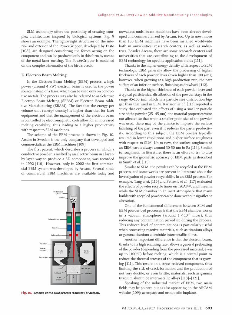
E. Electron Beam Melting
In the Electron Beam Melting (EBM) process, a high power (around 4 kW) electron beam is used as the power source instead of a laser, which can be used only on conduc-tive metals. The process may also be referred to as Selective Electron Beam Melting (SEBM) or Electron Beam Addi-tive Manufacturing (EBAM). The fact that the energy per volume unit (energy density) is higher than that for laser equipment and that the management of the electron beam is controlled by electromagnetic coils allow for an increased melting capability, thus leading to a higher productivity with respect to SLM machines.
The scheme of the EBM process is shown in Fig. 10. Arcam in Sweden is the only company that developed and commercializes the EBM machines [109].
The first patent, which describes a process in which a conductive powder is melted by an electric beam in a layer-by-layer way to produce a 3D component, was recorded in 1992 [110]. However, only in 2002 the first commer-cial EBM system was developed by Arcam. Several kinds of commercial EBM machines are available today and
nowadays multi-beam machines have been already devel-oped and commercialized by Arcam, too. Up to now, more than 150 EBM machines have been installed worldwide both in universities, research centers, as well as indus-tries. Besides Arcam, there are some research centers and universities that are contributing to the development of EBM technology for specific application fields [111].
Thanks to the higher energy density with respect to SLM technology, EBM generally allow the processing of higher thickness of each powder layer (even higher than 100 μm ); however, when growing at a high-production rate, the part suffers of an inferior surface, finishing as drawback [112].
Thanks to the higher thickness of each powder layer and a typical particle size, distribution of the powder stays in the range 45- 150 μm , which is a particle size distribution big-ger than that used in SLM. Karlsson et al. [113] reported a study that evaluated the effects of using a smaller particle size of the powder (25– 45 μm ): the material properties were not affected so that when a smaller grain size of the powder was used, there may be the chance to improve the surface finishing of the part even if it reduces the part’s productiv-ity. According to this subject, the EBM process typically resulted in lower resolutions and higher surface roughness with respect to SLM. Up to now, the surface roughness of an EBM part is always around 30- 50 μm in Ra [114]. Similar to roughness, in literature, there is an effort to try to also improve the geometric accuracy of EBM parts as described in Smith et al. [115].
Similar to SLM, the powder can be recycled in the EBM process, and some works are present in literature about the investigation of powder recyclability in an EBM process. For example, Tang et al. [116] and Petrovic et al. [117] evaluated the effects of powder recycle times on Ti6Al4V, and it seems while the SLM chamber in an inert atmosphere that many builds with recycled powder can be done without significant alteration.
One of the fundamental differences between SLM and EBM powder bed processes is that the EBM chamber works in a vacuum atmosphere (around 1 × 10 -5 mbar), thus reducing any contamination picked up during the process. This reduced level of contaminations is particularly useful when processing reactive materials, such as titanium alloys or gamma titanium aluminide intermetallic alloys.
Another important difference is that the electron beam, thanks to its high scanning rate, allows a general preheating of the powder (depending from the processed material, even up to 1100°C) before melting, which is a central point to reduce the thermal stresses of the component that is grow-ing [111]. This results in a stress-relieved component, thus limiting the risk of crack formation and the production of not very ductile, or even brittle, materials, such as gamma titanium aluminide intermetallic alloys [118]–[121].
Speaking of the industrial market of EBM, two main fields may be pointed out as also appearing on the ARCAM website [109]: aerospace and orthopedic implants.Fig. 10. Scheme of the EBM process (Courtesy of Arcam).

Calignano et al . : Overview on Additive Manufacturing Technologies
604 Proceedings of the IEEE | Vol. 105, No. 4, April 2017
With regard to orthopedic implants, EBM is used to produce parts, such as acetabular cups, knee, maxillofa-cial plates, hip, jaw replacements, etc. that are CE certi-fied since 2007 and gaining the approval from the United States Food and Drug Administration (FDA) since 2010 [122–126].
Nowadays, more than 40.000 titanium acetabular cups produced by EBM, with a porous surface for an improved osse-ointegration, have been implanted since April 2014, which is about 2% of the total manufacture of acetabular cups [111].
Two of the most used metals for the production by EBM of orthopedic implants are Ti6Al4V and CrCo, and several works are present in literature about these two materials that have been already well-reviewed by Sing et al. [122] and Murr et al. [127].
A central point of the suitability of EBM or the produc-tion of orthopedic implants is its great capability in the man-ufacture of porous (cellular) metallic structures [128]–[131] allowing a high regulation of pore size, strut diameter, and cell geometry. In addition, it integrates different porous structures in different parts of a single component. These EBM cellular structures have been extensively studied to ensure safe use in the human body: a brilliant behavior in compression [132], [133], a similar elastic modulus with respect to the human bones [134], [135] as well as a superior biocompatibility with promoting bone regeneration behav-ior [128] are reported.
Fig. 11 shows a Ti6Al4V implant (acetabular cup) with a surface design that was improved for osteointegration pro-vided by Arcam.
With regard to aerospace, one of the promising EBM applications that can be reported is related to feasibility of the process for gamma-TiAl alloys [118]–[121].
Actually, General Electric is currently using Ti48Al-2Cr2Nb intermetallic alloy in low-pressure turbine blades of the GEnex gas turbine engine designed for Boeing’s 787 Dreamliner [136]. For this reason, great attention is given to the possibility of applying EBM for the production of tita-nium aluminide low-pressure turbine blades in the aeroen-gine sector.
In relation to the route opened in the aeroengine sector with EBM and titanium aluminide components production, the automotive field might also be interested. Baudana et al. [137] evaluated the feasibility of titanium aluminide tur-bochargers for the automotive engine.
Other interesting applications of EBM in the aerospace sector that speak about complex components feasibility and testing are analyzed in the scientific literature [138], [139]. Liang et al. [138] proved the feasibility of an EBM and elec-trical discharge machining (EDM) combined method to produce shrouded blisks. EBM was used to generate a near-shape component of the final shrouded blisk, and EDM was used for finishing. The part is made of Ti6Al4V, and the evaluated mechanical properties are considered promising. The required blade accuracy was achieved, and through the combination of EBM and EDM method, the machining time of the shrouded blisk was greatly reduced. Tang et al. [139] designed and proved the feasibility with the EBM technol-ogy of a honeycomb rotor with hexagonal cone-shaped pore channels for oil and gas separation. The part is also made of Ti6Al4V.
As it is possible to see, Ti6Al4V is a well-established material for EBM technology whose microstructure and mechanical properties have been broadly investigated and already reviewed by [111], [129]. In general, the mechanical properties of Ti6Al4V fabricated by EBM are comparable to the properties of wrought Ti6Al4V and are higher than that of as-cast Ti6Al4V [140].
Other materials evaluated for the EBM process feasibility (apart from gamma-TiAl alloys described earler) are nickel superalloys, such as Inconel 718 and Inconel 625, Rene142, and CMSX4 [129, 141-144]; Cobalt superalloy [129], copper [129], [141], [145], stainless steels [111], [146], and CoCrMo [111], [147].
Recently, the EBM feasibility has been evaluated also for pure Niobium. Terrazas et al. evaluated the processabil-ity of high-purity niobium powder by EBM with the aim of manufacturing the new generation of superconducting radio frequency cavities. They are key components of lin-ear accelerators that are employed to transmit the energy necessary for the acceleration of subatomic particles, such as electrons [148].
With regard to the modelling of the EBM process, different approaches exist. In [149], [150], Korner et al. used the Lattice Boltzman Method (LBM) to calcu-late the temperature reached when processing Ti6Al4V powder. Nevertheless, this simulation approach is com-putationally intensive and consequently not very easy to use for the modelling of the entire EBM process. The second approach is the finite element method (FEM), which, considering the powder as a continuum with its own characteristics, seems to be more proper. The FEM approach is used in [151], [152] to predict stresses and distortions arising during the processing of Ti6Al4V by EBM. Similarly, the FEM approach is used in [153-156] to
Fig. 11. Ti6Al4V implant (acetabular cup) with surface design improved for osseointegration (Courtesy of Arcam).
Calignano et al . : Overview on Additive Manufacturing Technologies
Vol. 105, No. 4, April 2017 | Proceedings of the IEEE 605
calculate the temperature distribution in the powder bed modelling in the preheating phase of the EBM process as well as to determine the influence of different scanning strategies during melting.
A central point to fully exploiting AM technologies is the possibility of not only producing complex parts but also tailoring different microstructures (with different mechani-cal properties) on different zones of a complex component. This will be possible when the correlation among the tran-sient phenomena of repeated melting, the rapid solidifica-tion during the process, and the resulting microstructure is well understood, thus achieving an on-the-spot specific microstructure control within a manufactured part. Just as an example, experimental studies are available on the crys-tallographic texture control of Inconel 718 fabricated by EBM. Actually, Korner et al. [157] and Dehoff et al. [158] described the possibility to control, by changing the scan-ning strategy and/or process parameters, the formation of orientated columnar or near equiassic grains in different zones. In some recent studies, Price et al. [159], [160] used infrared thermal imaging techniques to measure the tem-perature distribution on the surface of the melt pool for microstructural engineering.
Although the control of the microstructure can be achieved experimentally by a trial-and-error correction of the process, this might require enormous and time-consum-ing work. However, in this regard, modelling of the process, as described earlier, has the potential to be a powerful tool, thus reducing the number of experimental trials. The works of Raghavan et al. [161] and Vastola et al. [162] are recent examples of this on Inconel 718 and Ti6Al4V, respectively.
Recently, also multimaterial components were fabri-cated by EBM and the joining interfaces were characterized. Hinojos et al. [163] explore the feasibility of the EBM pro-cess of Inconel 718 powder on top of a 316L stainless steel substrate and vice versa.
Another particular and interesting exploitation of the EBM process that is worth mentioning is reported by Hossain et al. [164]. They demonstrated that it is possible to use EBM technology to produce energy system components containing embedded piezoelectric sensors for in situ monitoring. In this paper, an interesting stop-and-go procedure was developed to achieve the goal of implanting piezoelectric ceramic sensors within metallic components at a specific height. The metallic component, built by EBM, contained a predesigned cavity for sensor placement within the part. The fabrication process was stopped at a desired height for sensor placement and allowed to continue until the part was complete.
III . EMERGING TECHNOLOGIES
Among the AM emerging technologies, the ones that are in development to realize fully dense monolithic ceramic sam-ples are not yet largely exploitable. In fact, in the case of ceramic materials, at the moment, the possibility to create
complex-shaped components with relevant physic- chemical properties is a real challenge [165]. Ceramics present some characteristics that limit their processing through AM methods. They are generally processed as powders, hav-ing high melting temperatures; they are brittle materials, and they have a poor resistance to thermal shocks. For these reasons, the direct interaction between a laser source and ceramic powders is rarely exploited not only for SLM but also for selective laser sintering (SLS). In fact, in the first case, laser energy is not able to reach the high melt-ing temperatures of technical ceramics. Up to now, the only ceramic material processed through SLM is based on alumina-zirconia eutectic mixtures that allow the reduction of melting temperatures at 1860 °C (condition reached with a preheating of the highly packed powder bed at 1600 °C in a homemade AM system) [166]. An indirect approach was often applied for SLM processing, adding to ceramic pow-ders other substances that when interacting with the laser develop a glassy phase, which consolidates the final compo-nent by embedding ceramic particles. In this case, contrary to traditional methods, the chemical composition of the ceramic system is modified during processing that in turn influences the final properties of the parts (generally lower), and no pure materials can be processed.
As stated, SLS processing of ceramic parts is also hardly feasible due to difficulties with consolidating them by exploiting sintering mechanisms. In general, ceramic den-sification requires high green density and long duration isotherms necessary for material diffusion at high tempera-tures, whereas in SLS systems, ceramic powders are gener-ally poorly packed (for their low flowability) and the process does not last enough to completely sinter them [165].
Up to now, the only AM technology able to realize dense ceramics with interesting mechanical features is based on SL: obviously in this case the liquid resin is filled with ceramic particles, with solid contents of 40– 65 vol%, and a sintering post-treatment is necessary to obtain the final part [167]. The exploitation of ceramic suspensions allows the processing of submicrometric and nanometric particles, adding dispersant and other substances to avoid agglomera-tion phenomena and to control liquid viscosity [165], [167], reachinch high green densities. To burn out the polymeric resin present in green components at the end of the print-ing, it is necessary to carry out a debinding thermal treat-ment prior to sintering. This step is very ticklish; therefore, customized thermal cycles must be defined on the basis of the used resins, because gaseous species could develop and create cracks and pores in ceramic walls, inducing part failure [168].
In the case of SL technology, some commercial solutions for ceramic materials are actually available, such as the sys-tems developed by Lithoz [169] or, starting in September 2016, by Admatec Europe BV [170]. These machines are able to cure the ceramic suspensions starting from a thin slurry layer deposited on a glass and building the part not

Calignano et al . : Overview on Additive Manufacturing Technologies
606 Proceedings of the IEEE | Vol. 105, No. 4, April 2017
REFERENCES
[1] J.-P. Kruth, M. C. Leu, and T. Nakagawa, “Progress in additive manufacturing and rapid prototyping,” CIRP Ann.-Manuf. Technol., vol. 47, no. 2, pp. 525–540, 1998.
[2] ASTM F2792-12a, “Standard Terminology for Additive Manufacturing Technologies,” (Withdrawn 2015) ASTM International, pp. 1–3, West Conshohocken, PA, 2012.
[3] V. Petrovic, J. V. H. Gonzalez, O. J. Ferrando, J. D. Gordillo, J. R. B. Puchades, and L. P. Griñan, “Additive layered manufacturing: Sectors of industrial application shown through case studies,” Int. J. Prod. Res., vol. 49, no. 4, pp. 1061–1079, 2011.
[4] N. Guo and M. C. Leu, “Additive manufacturing: Technology, applications and research needs,” Frontiers Mech. Eng., vol. 8, no. 3, pp. 215–243, Sep. 2013.
[5] B. Lyons, “Additive manufacturing in aerospace: Examples and research outlook,” Bridge, Linking Eng. Soc., vol. 42, no. 1, pp. 13–19, 2012.
[6] C. C. Sandström, “Adopting 3D printing for manufacturing—Evidence from the hearing aid industry,” Technol. Forecasting Social Change, vol. 102, pp. 160–168, 2015.
[7] B. Sanz-Izquierdo and E. A. Parker, “3D printing technique for fabrication of frequency selective structures for built environment,” Electron. Lett., vol. 49, no. 18, pp. 1117–1118, Aug. 2013.
[8] L. T. Nassar and T. M. Weller, “An electrically-small, 3-D cube antenna fabricated with additive manufacturing,” in Proc. Radio Wireless Symp., Jan. 2013, pp. 262–264.
[9] A. M. N. Ai-Mobin, R. Shankar, W. Cross, J. Kellar, K. W. Whites, and D. E. Anagnostou, “Advances in direct-write printing of RF-MEMS using M3D,” in IEEE MTT-S Int. Microw. Symp. Dig., Jun. 2014, pp. 1–6.
[10] C. J. Kief et al., “Printing multi-functionality: Additive manufacturing for CubeSats,” in Proc. AIAA SPACE Conf. Expo., San Diego, CA, USA, 2014, pp. 1–9, doi: 10.2514/6.2014-4193.
[11] T. Merkle, R. Götzen, J. Y. Choi, and S. Koch, “Polymer multichip module process using 3-D printing technologies for D-band applications,” IEEE Trans. Microw. Theory Techn., vol. 63, no. 2, pp. 481–493, Feb. 2015.
[12] E. D. Cullens, L. Ranzani, K. J. Vanhille, E. N. Grossman, N. Ehsan, and Z. Popovic, “Micro-fabricated 130–180 GHz frequency scanning waveguide arrays,” IEEE Trans. Antennas Propag., vol. 60, no. 8, pp. 3647–3653, Aug. 2012.
fully immersed in the liquid feedstock, thus lowering the process costs and consumption of raw materials.
I V. SATELLITE A PPLIC ATIONS
Supported by the recent developments of design optimi-zation tools and manufacturing capabilities, components and parts produced using AM are emerging in the space industry. Decisive factors in the space industry are the weight reduction (every ounce saved is an ounce that does not have to be launched into space) and how the compo-nent performs under extremely harsh conditions in space and during the launch procedure. Therefore, the compo-nent does not only have to be light but also extremely stiff. Another factor is that these parts for satellite applications are typically made of materials that are hard to machine and are made in low quantities. A key simulation technol-ogy being leveraged to shorten the design cycle for AM is Topology Optimization, a nonparametric optimization technique that identifies and removes areas of a design space not contributing to the stiffness of the part or to the part load path.
The current generation of satellites includes specific brackets that serve as a link between the body of the satel-lite and the reflectors. By combining topology optimization techniques with AM technologies, new brackets are actually produced as structural brackets for Eurostar E3000 (Airbus Defence and Space) telecommunications satellites manu-factured from aluminium alloy (Fig. 12). In contrast to the previous bracket that consists of four parts and 44 rivets, the AM bracket is a single piece obtained by laser melting and has a weight 35% lower than that of the previous component and an increase in stiffness of 40%.
RUAG Space, in conjunction with Altair ProductDesign, has developed an antenna bracket (40 cm long) in alumin-ium alloy that is one of the longest metal components ever produced using laser melting technology.
Airbus Defence and Space has developed a new bracket in titanium alloy: the entire structure can easily withstand a span of 330°C under a force of 20kN.
FDM technology was also used for microwave applica-tions to develop planar and nonplanar conformal antennas. In particular, the dielectric layers and the metallic structures of the antennas are printed via multimaterial AM systems: FDM of thermoplastic polymers with micro-dispensing of conductive inks [172].
V. CONCLUSION
AM technology has begun to show great potential and advan-tages in many industrial fields by providing an efficient solu-tion to producing low volume, customized products with complex geometries using materials with properties com-parable, if not higher, to those obtained using traditional manufacturing.
Despite the fact that some additive technologies, such as the SL process, were introduced many years ago, the research and development work is still ongoing to try to fine-tune the various AM technologies and understand the physical phenomena associated with them during the crea-tion of the part, to expand the usable materials, and explore the fabrication of complex integrated systems.
Fig. 12. Eurostar E3000 bracket (Source: Airbus Defence and Space Ltd [171]).

Calignano et al . : Overview on Additive Manufacturing Technologies
Vol. 105, No. 4, April 2017 | Proceedings of the IEEE 607
[13] “Wohlers Report 2014—3D Printing and Additive Manufacturing State of the Industry, Annual Worldwide Progress Report”, Wohlers Associates, Cary, NC, USA, 2014.
[14] B. N. Turner, R. Strong, and S. A. Gold, “A review of melt extrusion additive manufacturing processes: I. Process design and modeling,” Rapid Prototyping J., vol. 20, no. 3, pp. 192–204, 2014.
[15] Arevo Labs, [Online]. Available: http://www.arevolabs.com
[16] Igus, [Online]. Available: http://www.igus.com
[17] C. J. L. Pérez, “Analysis of the surface roughness and dimensional accuracy capability of fused deposition modelling processes,” Int. J. Prod. Res., vol. 40, no. 12, pp. 2865–2881, 2002.
[18] N. S. A. Bakar, M. R. Alkahari, and H. Boejang, “Analysis on fused deposition modelling performance,” J. Zhejiang Univ.-Sci. A, vol. 11, no. 12, pp. 972–977, Dec. 2010.
[19] P. Minetola, L. Iuliano, E. Bassoli, and A. Gatto, “Impact of additive manufacturing on engineering education—Evidence from Italy,” Rapid Prototyping J., vol. 21, no. 5, pp. 535–555, 2015.
[20] Stratasys, Ltd., [Online]. Available: http://www.stratasys.com
[21] R. Anitha, S. Arunachalam, and P. Radhakrishnan, “Critical parameters influencing the quality of prototypes in fused deposition modelling,” J. Mater. Process. Technol., vol. 118, nos. 1–3, pp. 385–388, Dec. 2001.
[22] C. J. L. Pérez, “Analysis of the surface roughness and dimensional accuracy capability of fused deposition modelling processes,” Int. J. Prod. Res., vol. 40, no. 12, pp. 2865–2881, 2002.
[23] R. Singh, “Process capability analysis of fused deposition modelling for plastic components,” Rapid Prototyping J., vol. 20, no. 1, pp. 69–76, 2014.
[24] B. N. Turner and S. A. Gold, “A review of melt extrusion additive manufacturing processes: II. Materials, dimensional accuracy, and surface roughness,” Rapid Prototyping J., vol. 21, no. 3, pp. 250–261, 2015.
[25] P. Minetola, L. Iuliano, and G. Marchiandi, “Benchmarking of FDM machines through part quality using IT grades,” Procedia CIRP, vol. 41, pp. 1027–1032, 2016.
[26] L. M. Galantucci, F. Lavecchia, and G. Percoco, “Experimental study aiming to enhance the surface finish of fused deposition modeled parts,” CIRP Ann.-Manuf. Technol., vol. 58, no. 1, pp. 189–192, Dec. 2009.
[27] L. M. Galantucci, F. Lavecchia, and G. Percoco, “Quantitative analysis of a chemical treatment to reduce roughness of parts fabricated using fused deposition modeling,” CIRP Ann.-Manuf. Technol., vol. 59, no. 1, pp. 247–250, Dec. 2010.
[28] A. Garg, A. Bhattacharya, and A. Batish, “On surface finish and dimensional accuracy of FDM parts after cold vapor treatment,” Mater. Manuf. Process., vol. 31, no. 4, pp. 522–529, Jul. 2015.
[29] R. Ilardo and C. B. Williams, “Design and manufacture of a formula SAE intake system using fused deposition modeling and fiber-reinforced composite materials,” Rapid Prototyping J., vol. 16, no. 3, pp. 174–179, Apr. 2010.
[30] S. Daneshmand, C. Aghanajafi, and H. Shahverdi, “Investigation of rapid manufacturing technology with ABS material for wind tunnel models fabrication,” J. Polym. Eng., vol. 32, nos. 8–9, pp. 575–584, Dec. 2012.
[31] P. Dudek, “FDM 3D printing technology in manufacturing composite elements,” Arch. Metall. Mater., vol. 58, no. 4, pp. 1415–1418, Dec. 2013.
[32] M. Vermeulen et al., “Manufacturing of patient-specific optically accessible airway models by fused deposition modeling,” Rapid Prototyping J., vol. 19, no. 5, pp. 312–318, 2013.
[33] R. Madani, A. Moroz, and E. Baines, “Design and manufacturing of children’s remote control for child viewing,” Adv. Prod. Eng. Manage., vol. 8, no. 2, pp. 116–125, Jun. 2013.
[34] R. Singh and G. Singh, “Investigations for statistically controlled investment casting solution of FDM-based ABS replicas,” Rapid Prototyping J., vol. 20, no. 3, pp. 215–220, Apr. 2014.
[35] Y. Gür, “Additive manufacturing of anatomical models from computed tomography scan data,” Molecular Cellular Biomech., vol. 11, no. 4, pp. 249–258, Dec. 2014.
[36] V. A. Lifton, G. Lifton, and S. Simon, “Options for additive rapid prototyping methods (3D printing) in MEMS technology,” Rapid Prototyping J., vol. 20, no. 5, pp. 403–412, Aug. 2014.
[37] K. S. Boparai, R. Singh, and H. Singh, “Development of rapid tooling using fused deposition modeling: A review,” Rapid Prototyping J., vol. 22, no. 2, pp. 281–299, 2016.
[38] S. Bose, J. Darsell, H. L. Hosick, L. Yang, D. K. Sarkar, and A. Bandyopadhyay, “Processing and characterization of porous alumina scaffolds,” J. Mater. Sci., Mater. Med., vol. 13, no. 1, pp. 23–28, Jan. 2002.
[39] A. Bellini, L. Shor, and S. I. Guceri, “New developments in fused deposition modeling of ceramics,” Rapid Prototyping J., vol. 11, no. 4, pp. 214–220, Sep. 2005.
[40] I. Grida and J. R. G. Evans, “Extrusion freeforming of ceramics through fine nozzles,” J. Eur. Ceram. Soc., vol. 23, no. 5, pp. 629–635, Apr. 2003.
[41] M. Hirsch, T. McGuire, M. Parsons, S. Leake, and J. Straub, “Enabling homeland security missions with in-space 3D printing,” Proc. SPIE, vol. 9854, pp. 98250C-1–98250C-7, May 2016.
[42] M. Parsons, T. McGuire, M. Hirsch, S. Leake, and J. Straub, “Enablement of defense missions with in-space 3D printing,” Proc. SPIE, vol. 9838, pp. 98380U-1–98380U-6, May 2016.
[43] T. McGuire, M. Hirsch, M. Parsons, S. Leake, and J. Straub, “Enablement of scientific remote sensing missions with in-space 3D printing,” Proc. SPIE, vol. 9825, pp. 985413-1–985413-9, May 2016.
[44] J. Y. Wong, “3D printing applications for space missions,” Aerosp. Med. Human Perform., vol. 87, no. 6, pp. 580–582, Jun. 2016.
[45] I. Gibson, D. Rosen, and B. Stucker, Additive Manufacturing Technologies. New York, NY, USA: Springer Science, 2010.
[46] F. Gao and A. A. Sonin, “Precise deposition of molten microdrops: The physics of digital microfabrication,” Proc. R. Soc. Lond. A, Math. Phys. Sci., vol. 444, pp. 533–554, Mar. 1994.
[47] N. Reis, K. A. M. Seerden, B. Derby, J. W. Halloran, and J. R. G. Evans, “Direct inkjet deposition of ceramic green bodies: II—Jet behaviour and deposit formation,” in Proc. Mater. Res. Soc. Symp., vol. 542, pp. 147–152, 1999.
[48] W. Feng, J. Y. H. Fuh, and Y. S. Wong, “Development of a drop-on-demand micro dispensing system,” Mater. Sci. Forum, vols. 505–507, pp. 25–30, Jan. 2006.
[49] T. Shimoda, K. Morii, S. Seki, and H. Kiguchi, “Inkjet printing of light-emitting polymer displays,” MRS Bull., vol. 28, no. 11, pp. 821–827, Nov. 2003.
[50] J. Perelaer et al., “Printed electronics: The challenges involved in printing devices, interconnects, and contacts based on inorganic materials,” J. Mater. Chem., vol. 20, no. 39, pp. 8446–8453, 2010.
[51] K. A. M. Seerden, N. Reis, J. R. G. Evans, P. S. Grant, J. W. Halloran, and B. Derby, “Ink-jet printing of wax-based alumina suspensions,” J. Amer. Ceram. Soc., vol. 84, no. 11, pp. 2514–2520, Nov. 2001.
[52] B. Derby, “Printing and prototyping of tissues and scaffolds,” Science, vol. 338, no. 6109, pp. 921–926, Nov. 2012.
[53] R. E. Camley and R. L. Stamps, Eds., Solid State Physics, vol. 66. Amsterdam, The Netherlands: Elsevier, 2015.
[54] 3D Systems, Inc., [Online]. Available: http://www.3dsystems.com/
[55] J. J. Beaman et al., Solid Freeform Fabrication: A New Direction in Manufacturing: With Research and Applications in Thermal Laser Processing. New York, NY, USA: Springer, 2013.
[56] F. P. W. Melchels, J. Feijen, and D. W. Grijpma, “A review on stereolithography and its applications in biomedical engineering,” Biomaterials, vol. 31, no. 24, pp. 6121–6130, 2010.
[57] A. Bens et al., “Non-toxic flexible photopolymers for medical stereolithography technology,” Rapid Prototyping J., vol. 13, no. 1, pp. 38–47, 2007.
[58] C. Hinczewski, S. Corbel, and T. Chartier, “Ceramic suspensions suitable for stereolithography,” J. Eur. Ceram. Soc., vol. 18, no. 6, pp. 583–590, 1998.
[59] A. Badev et al., “Photopolymerization kinetics of a polyether acrylate in the presence of ceramic fillers used in stereolithography,” J. Photochem. Photobiol. A, Chem., vol. 222, no. 1, pp. 117–122, 2011.
[60] T. Chartier, A. Badev, Y. Abouliatim, P. Lebaudy, and L. Lecamp, “Stereolithography process: Influence of the rheology of silica suspensions and of the medium on polymerization kinetics—Cured depth and width,” J. Eur. Ceram. Soc., vol. 32, no. 8, pp. 1625–1634, 2012.
[61] A. V. Lifton, G. Lifton, and S. Simon, “Options for additive rapid prototyping methods (3D printing) in MEMS technology,” Rapid Prototyping J., vol. 20, no. 5, pp. 403–412, 2014.
[62] B. Luan, M. Yeung, W. Wells, and X. Liu, “Chemical surface preparation for metallization of stereolithography polymers,” Appl. Surf. Sci., vol. 156, nos. 1–4, pp. 26–38, 2000.
[63] P. S. Gandhi and S. Deshmukh, “A 2D optomechanical focused laser spot scanner: Analysis and experimental results for microstereolithography,” J. Micromech. Microeng., vol. 20, no. 1, p. 015035, 2010.

Calignano et al . : Overview on Additive Manufacturing Technologies
608 Proceedings of the IEEE | Vol. 105, No. 4, April 2017
[64] A. Bertsch and P. Renaud, “Microstereolithography A2—Baldacchini, Tommaso,” in Three-Dimensional Microfabrication Using Two-photon Polymerization. Oxford, U.K.: William Andrew Publishing, 2016, ch. 1.2, pp. 20–44.
[65] S. Deshmukh and P. S. Gandhi, “Optomechanical scanning systems for microstereolithography (MSL): Analysis and experimental verification,” J. Mater. Process. Technol., vol. 209, no. 3, pp. 1275–1285, 2009.
[66] H. Kim, J.-W. Choi, and R. Wicker, “Scheduling and process planning for multiple material stereolithography,” Rapid Prototyping J., vol. 16, no. 4, pp. 232–240, 2010.
[67] A. J. Lopes, I. H. Lee, E. MacDonald, R. Quintana, and R. Wicker, “Laser curing of silver-based conductive inks for in situ 3D structural electronics fabrication in stereolithography,” J. Mater. Process. Technol., vol. 214, no. 9, pp. 1935–1945, 2014.
[68] A. J. Lopes, E. MacDonald, and R. B. Wicker, “Integrating stereolithography and direct print technologies for 3D structural electronics fabrication,” Rapid Prototyping J., vol. 18, no. 2, pp. 129–143, 2012.
[69] F. Gimenez, S. Corbel, J. F. Chassagne, and M. L. Viriot, “Bone reconstruction with laser stereolithography,” in Proc. 1st Joint Eng. Med. Biol., 21st Annu. Conf. Annu. Fall Meeting Biomed. Eng. Soc. (BMES/EMBS), 1999, p. 832.
[70] D. Yourtee, J. Emery, R. E. Smith, and B. Hodgson, “Stereolithographic models of biopolymers,” J. Molecular Graph. Model., vol. 18, no. 1, pp. 26–28, 2000.
[71] J. F. Bouyssié, S. Bouyssié, P. Sharrock, and D. Duran, “Stereolithographic models derived from X-ray computed tomography reproduction accuracy,” Surgical Radiol. Anatomy, vol. 19, no. 3, pp. 193–199, 1997.
[72] D. Rohner, R. Gui´jarro-Martínez, P. Bucher, and B. Hammer, “Importance of patient-specific intraoperative guides in complex maxillofacial reconstruction,” J. Cranio-Maxillofacial Surgery, vol. 41, no. 5, pp. 382–390, 2013.
[73] D. Du, T. Asaoka, T. Ushida, and K. S. Furukawa, “Fabrication and perfusion culture of anatomically shaped artificial bone using stereolithography,” Biofabrication, vol. 6, no. 4, p. 045002, 2014.
[74] W. C. Scarfe, “The language of reality,” Oral Surgery, Oral Med., Oral Pathol. Oral Radiol., vol. 120, no. 3, pp. 281–283, 2015.
[75] S. Nayar, S. Bhuminathan, and W. M. Bhat, “Rapid prototyping and stereolithography in dentistry,” J. Pharmacy Bioallied Sci., vol. 7, no. 1, pp. S216–S219, 2015.
[76] T. Kurzynowski, E. Chlebus, B. Kuznicka, and J. Reiner, “Parameters in selective laser melting for processing metallic powders,” Proc. SPIE, vol. 8239, p. 823914, Feb. 2012, doi: 10.1117/12.907292.
[77] R. Li, J. Liu, Y. Shi, L. Wang, and W. Jiang, “Balling behavior of stainless steel and nickel powder during selective laser melting process,” Int. J. Adv. Manuf. Technol, vol. 59, pp. 1025–1035, Apr. 2011.
[78] M. M. Van Elsen, “Complexity of selective laser melting: A new optimization approach,” Ph.D. dissertation, Department of Mechanical Engineering, Katholieke Univ. Leuven, Leuven, Belgium, 2007.
[79] F. Niebling, A. Otto, and M. Geiger, “Analyzing the DMLS-process by a macroscopic FE-model,” in Proc. 13th Solid Freeform Fabrication Symp., 2002, pp. 384–391.
[80] J.-P. Kruth, L. Froyen, J. Van Vaerenbergh, P. Mercelis, M. Rombouts, and B. Lauwers, “Selective laser melting of iron-based powder,” J. Mater. Process. Technol., vol. 149, pp. 616–622, Jun. 2014.
[81] C. Hauser et al., “Direct selective laser sintering of tool steel powders to high density. Part A: Effects of laser beam width and scan strategy,” in Proc. 14th Solid Freeform Fabrication Symp., 2003, pp. 644–655.
[82] P. Lott, H. Schleifenbaum, W. Meiners, K. Wissenbach, C. Hinke, and J. Bültmann, “Design of an optical system for the in situ process monitoring of selective laser melting (SLM),” Phys. Procedia, vol. 12, pp. 683–690, 2011.
[83] B. Van der Schueren and J.-P. Kruth, “Powder deposition in selective metal powder sintering,” Rapid Prototyping J., vol. 1, no. 3, pp. 23–31, 1995.
[84] M. van Elsen, F. Al-Bender, and J.-P. Kruth, “Application of dimensional analysis to selective laser melting,” Rapid Prototyping J., vol. 14, no. 1, pp. 15–22, 2008.
[85] F. Calignano, D. Manfredi, E. P. Ambrosio, L. Iuliano, and P. Fino, “Influence of process parameters on surface roughness of aluminum parts produced by DMLS,” Int. J. Adv. Manuf. Technol., vol. 67, no. 9, pp. 2743–2751, 2013.
[86] J.-P. Kruth, M. Badrossamay, E. Yasa, J. Deckers, L. Thijs, and J. Van Humbeeck, “Part and material properties in selective laser melting of metals,” in Proc. 16th Int. Symp. Electromach., 2010, pp. 1–12.
[87] K. Alrbaey, D. Wimpenny, R. Tosi, W. Manning, and A. Moroz, “On optimization of surface roughness of selective laser melted stainless steel parts: A statistical study,” J. Mater. Eng. Perform., vol. 23, no. 6, pp. 2139–2148, 2014.
[88] I. Yadroitsev and I. Smurov, “Surface morphology in selective laser melting of metal powders,” Phys. Procedia, vol. 12, pp. 264–270, 2011.
[89] ASM Handbook: Properties and Selection: Irons, Steels, and High-Performance Alloys, vol. 1. Materials Park, OH, USA: ASM International, 1990, pp. 1303–1408.
[90] G. Miranda et al., “Predictive models for physical and mechanical properties of 316L stainless steel produced by selective laser melting,” Mater. Sci. Eng. A, vol. 657, pp. 43–56, Mar. 2016.
[91] M. M. Dewidar, K. A. Khalil, and J. K. Lim, “Processing and mechanical properties of porous 316L stainless steel for biomedical applications,” Trans. Nonferrous Met. Soc. China, vol. 17, no. 3, pp. 468–473, 2007.
[92] H. Wang, M. A. Sweikart, and J. A. Turner, “Stainless steel as bipolar plate material for polymer electrolyte membrane fuel cells,” J. Power Sour., vol. 115, no. 2, pp. 243–251, 2003.
[93] F.-L. Xu, J.-Z. Duan, C.-G. Lin, and B.-R. Hou, “Influence of marine aerobic biofilms on corrosion of 316L stainless steel,” J. Iron Steel Res. Int., vol. 22, no. 8, pp. 715–720, 2015.
[94] J. C. Wataha and G. Schmalz, “Dental alloys,” in Biocompatibility of Dental Materials. Berlin, Germany: Springer, 2009, pp. 221–254.
[95] S. Y. Hedberg, B. Qian, Z. Shen, S. Virtanen, and I. O. Wallinder, “In vitro biocompatibility of CoCrMo dental alloys fabricated by selective laser melting,” Dental Mater., vol. 30, no. 5, pp. 525–534, 2014.
[96] A. Takaichi et al., “Microstructures and mechanical properties of Co–29Cr–6Mo alloy fabricated by selective laser melting process for dental applications,” J. Mech. Behavior Biomed. Mater., vol. 21, pp. 67–76, May 2013.
[97] G. Barucca et al., “Structural characterization of biomedical Co–Cr–Mo components produced by direct metal laser sintering,” Mater. Sci. Eng. C, vol. 48, pp. 263–269, Mar. 2015.
[98] E. Chlebus, K. Gruber, B. Kuxnicka, J. Kurzac, and T. Kurzynowski, “Effect of heat treatment on the microstructure and mechanical properties of Inconel 718 processed by selective laser melting,” Mater. Sci. Eng. A, vol. 639, pp. 647–655, Jul. 2015.
[99] D. Manfredi et al., “Additive manufacturing of Al alloys and aluminium matrix composites (AMCs),” in Light Metal Alloys Applications, W. A. Monteiro, Ed. Rijeka, Croatia: InTech, 2014, pp. 3–34.
[100] F. Calignano, “Design optimization of supports for overhanging structures in aluminum and titanium alloys by selective laser melting,” Mater. Des., vol. 64, pp. 203–213, Dec. 2014.
[101] E. O. Olakanmi, “Selective laser sintering/melting (SLS/SLM) of pure Al, Al–Mg, and Al–Si powders: Effect of processing conditions and powder properties,” J. Mater. Process. Technol., vol. 213, pp. 1387–1405, Aug. 2013.
[102] E. Brandl, U. Heckenberger, V. Holzinger, and D. Buchbinder, “Additive manufactured AlSi10Mg samples using selective laser melting (SLM): Microstructure, high cycle fatigue, and fracture behavior,” Mater. Des., vol. 34, pp. 159–169, Feb. 2012.
[103] S. Siddique, M. Imran, E. Wycisk, C. Emmelmann, and F. Walther, “Influence of process-induced microstructure and imperfections on mechanical properties of AlSi12 processed by selective laser melting,” J. Mater. Process. Technol., vol. 221, pp. 205–213, Jul. 2015.
[104] Y. Zhou et al., “A novel titanium alloy manufactured by selective laser melting: Microstructure, high temperature oxidation resistance,” Mater. Des., vol. 89, pp. 1199–1204, Jan. 2016.
[105] D. K. Pattanayak et al., “Bioactive Ti metal analogous to human cancellous bone: Fabrication by selective laser melting and chemical treatments,” Acta Biomater., vol. 7, no. 3, pp. 1398–1406, 2011.
[106] T. Vilaro, C. Colin, and J. D. Bartout, “As-fabricated and heat-treated microstructures of the Ti–6Al–4V alloy processed by selective laser melting,” Metall. Mater. Trans. A, vol. 42, pp. 3190–3199, Oct. 2011.
[107] L. S. Bertol, W. Kindlein, Jr., F. P. da Silva, and C. Aumund-Kopp, “Medical design: Direct metal laser sintering of Ti–6Al–4V,” Mater. Des., vol. 31, no. 8, pp. 3982–3988, 2010.
[108] Festo Group, [Online]. Available: http://www.festo.com
[109] Arcam AB, [Online]. Available: http://www.arcam.com/
[110] R. Larson, “Method and device for producing three-dimensional bodies,” WO Patent 1994026446 A1, 1994.

Calignano et al . : Overview on Additive Manufacturing Technologies
Vol. 105, No. 4, April 2017 | Proceedings of the IEEE 609
[111] J. Wang and H. Tang, “Review on metals additively manufactured by SEBM,” Mater. Technol., Adv. Perform. Mater., vol. 31, no. 2, pp. 86–89, 2016.
[112] N. Guo and M. C. Leu, “Additive manufacturing: Technology, applications and research needs,” Frontiers Mech. Eng., vol. 8, no. 3, pp. 215–243, 2013.
[113] J. Karlsson, A. Snis, H. Engqvist, and J. Lausmaa, “Characterization and comparison of materials produced by electron beam melting (EBM) of two different Ti–6Al–4V powder fractions,” J. Mater. Process. Technol., vol. 213, no. 12, pp. 2109–2118, 2013.
[114] J. K. Algardh et al., “Thickness dependency of mechanical properties for thin-walled titanium parts manufactured by electron beam melting (EBM),” Additive Manuf., vol. 12, pp. 45–50, Oct. 2016.
[115] C. J. Smith et al., “Dimensional accuracy of electron beam melting (EBM) additive manufacture with regard to weight optimized truss structures,” J. Mater. Process. Technol., vol. 229, pp. 128–138, Mar. 2016.
[116] H. P. Tang, M. Qian, N. Liu, X. Z. Zhang, G. Y. Yang, and J. Wang, “Effect of powder reuse times on additive manufacturing of Ti-6Al-4V by selective electron beam melting,” JOM, vol. 67, no. 3, pp. 555–563, 2015.
[117] V. Petrovic and R. Niñerola, “Powder recyclability in electron beam melting for aeronautical use,” Aircraft Eng. Aerosp. Technol. Int. J., vol. 87, no. 2, pp. 147–155, 2015.
[118] H. P. Tang, G. Y. Yang, W. P. Jia, W. W. He, S. L. Lu, and M. Qian, “Additive manufacturing of a high niobium-containing titanium aluminide alloy by selective electron beam melting,” Mater. Sci. Eng. A, vol. 636, pp. 103–107, Jun. 2015.
[119] S. Biamino et al., “Electron beam melting of Ti–48Al–2Cr–2Nb alloy: Microstructure and mechanical properties investigation,” Intermetallics, vol. 19, no. 6, pp. 776–787, 2011.
[120] L. E. Murr et al., “Characterization of titanium aluminide alloy components fabricated by additive manufacturing using electron beam melting,” Acta Mater., vol. 58, no. 5, pp. 1887–1894, 2010.
[121] J. Schwerdtfeger and C. Körrner, “Selective electron beam melting of Ti–48Al–2Nb–2Cr: Microstructure and aluminium loss,” Intermetallics, vol. 49, pp. 29–35, Jun. 2014.
[122] S. L. Sing, J. An, W. Y. Yeong, and F. E. Wiria, “Laser and electron-beam powder-bed additive manufacturing of metallic implants: A review on processes, materials and designs,” J. Orthopaedic Res., vol. 34, no. 3, pp. 369–385, 2016.
[123] M. Cronskär, M. Bäckström, and L. E. Rännar, “Production of customized hip stem prostheses—A comparison between conventional machining and electron beam melting (EBM),” Rapid Prototyping J., vol. 19, no. 5, pp. 365–372, 2013.
[124] A. Mazzoli, M. Germani, and R. Raffaeli, “Direct fabrication through electron beam melting technology of custom cranial implants designed in a PHANToM-based haptic environment,” Mater. Design, vol. 30, no. 8, pp. 3186–3192, 2009.
[125] A. L. Jardini et al., “Customised titanium implant fabricated in additive manufacturing for craniomaxillofacial surgery,” Virtual Phys. Prototyping, vol. 9, no. 2, pp. 115–125, 2014.
[126] A. L. Jardini et al., “Cranial reconstruction: 3D biomodel and custom-built implant created using additive manufacturing,” J. Cranio-Maxillofacial Surgery, vol. 42, no. 8, pp. 1877–1884, 2014.
[127] L. E. Murr, S. M. Gaytan, E. Martinez, F. Medina, and R. B. Wicker, “Next generation orthopaedic implants by additive manufacturing using electron beam melting,” Int. J. Biomater., vol. 2012, pp. 1–14, Jun. 2012.
[128] S. Zhao, S. J. Li, W. T. Hou, Y. L. Hao, R. Yang, and R. D. K. Misra, “The influence of cell morphology on the compressive fatigue behavior of Ti-6Al-4V meshes fabricated by electron beam melting,” J. Mech. Behavior Biomed. Mater., vol. 59, pp. 251–264, Jun. 2016.
[129] L. E. Murr et al., “Metal fabrication by additive manufacturing using laser and electron beam melting technologies,” J. Mater. Sci. Technol., vol. 28, no. 1, pp. 1–14, 2012.
[130] L. E. Murr et al., “Microstructure and mechanical properties of open-cellular biomaterials prototypes for total knee replacement implants fabricated by electron beam melting,” J. Mech. Behavior Biomed. Mater., vol. 4, no. 7, pp. 1396–1411, 2011.
[131] E. Marin, S. Fusi, M. Pressacco, L. Paussa, and L. Fedrizzi, “Characterization of cellular solids in Ti6Al4V for orthopaedic implant applications: Trabecular titanium,” J. Mech. Behavior Biomed. Mater., vol. 3, no. 5, pp. 373–381, 2010.
[132] X. Y. Cheng et al., “Compression deformation behavior of Ti–6Al–4V alloy with cellular structures fabricated by electron beam melting,” J. Mech. Behavior Biomed. Mater., vol. 16, no. 1, pp. 153–162, 2012.
[133] J. Parthasarathy, B. Starly, S. Raman, and A. Christensen, “Mechanical evaluation of porous titanium (Ti6Al4V) structures with electron beam melting (EBM),” J. Mech. Behavior Biomed. Mater., vol. 3, no. 3, pp. 249–259, 2010.
[134] L. E. Murr et al., “Next-generation biomedical implants using additive manufacturing of complex, cellular and functional mesh arrays,” Philos. Trans. Roy. Soc. London A, Math. Phys. Sci., vol. 368, pp. 1999–2032, Mar. 2010.
[135] L. E. Murr et al., “Characterization of Ti–6Al–4V open cellular foams fabricated by additive manufacturing using electron beam melting,” Mater. Sci. Eng. A, vol. 527, nos. 7–8, pp. 1861–1868, 2010.
[136] GE Aviation. GE-viation: GEnx. (2007). [Online]. Available: http://www.geae.com/engines/commercial/genx/
[137] G. Baudana et al., “Electron beam melting of Ti-48Al-2Nb-0.7Cr-0.3Si: Feasibility investigation,” Intermetallics, vol. 73, pp. 43–49, Jun. 2016.
[138] W. Liang, X. Kang, W. Zhao, and Y. Yang, “Electrical discharge machining of electron beam melting formed shrouded blisk,” Int. J. Adv. Manuf. Technol., vol. 87, no. 5, pp. 2319–2326, 2016.
[139] H. P. Tang et al., “A honeycomb-structured Ti-6Al-4V oil–gas separation rotor additively manufactured by selective electron beam melting for aero-engine applications,” JOM, vol. 68, no. 3, pp. 799–805, 2016.
[140] L. Murr et al., “Microstructures and mechanical properties of electron beam-rapid manufactured Ti–6Al–4V biomedical prototypes compared to wrought Ti–6Al–4V,” Mater. Characterization, vol. 60, no. 2, pp. 96–105, 2009.
[141] L. E. Murr et al., “Fabrication of metal and alloy components by additive manufacturing: Examples of 3D materials science,” J. Mater. Res. Technol., vol. 1, no. 1, pp. 42–54, 2012.
[142] L. E. Murr et al., “Microstructures of rene 142 nickel-based superalloy fabricated by electron beam melting,” Acta Mater., vol. 61, no. 11, pp. 4289–4296, 2013.
[143] M. Ramsperger, R. F. Singer, and C. Korner, “Microstructure of the nickel-base superalloy CMSX-4 fabricated by selective electron beam melting,” Metall. Mater. Trans. A, vol. 47, no. 3, pp. 1469–1480, 2016.
[144] H. E. Helmer, C. Körner, and R. F. Singer, “Additive manufacturing of nickel-based superalloy Inconel 718 by selective electron beam melting: Processing window and microstructure,” J. Mater. Res., vol. 29, no. 17, pp. 1987–1996, 2014.
[145] M. A. Lodes, R. Guschlbauer, and C. Körner, “Process development for the manufacturing of 99.94% pure copper via selective electron beam melting,” Mater. Lett., vol. 143, pp. 298–301, Mar. 2015.
[146] H. B. Qi, Y. N. Yan, F. W. He, and R. J. Zhang, “Direct metal part forming of 316L stainless steel powder by electron beam selective melting,” Proc. Inst. Mech. Eng., B, J. Eng. Manuf., vol. 220, no. 11, pp. 1845–1853, 2006.
[147] S. H. Sun, Y. Koizumi, S. Kurosu, Y. P. Li, H. Matsumoto, and A. Chiba, “Build direction dependence of microstructure and high-temperature tensile property of Co–Cr–Mo alloy fabricated by electron beam melting,” Acta Mater., vol. 64, pp. 154–168, Feb. 2014.
[148] C. A. Terrazas et al., “Fabrication and characterization of high-purity niobium using electron beam melting additive manufacturing technology,” Int. J. Adv. Manuf. Technol., vol. 84, no. 5, pp. 1115–1126, 2016.
[149] R. Ammer, U. Rüde, M. Markl, V. K. Jüchter, and C. C. Körner, “Validation experiments for LBM simulations of electron beam melting,” Int. J. Modern Phys. C, vol. 25, no. 12, p. 1441009, 2014.
[150] C. C. Körner, E. Attar, and P. Heinl, “Mesoscopic simulation of selective beam melting processes,” J. Mater. Process. Technol., vol. 211, no. 6, pp. 978–987, 2011.
[151] E. R. Denlinger, J. C. Heigel, and P. Michaleris, “Residual stress and distortion modeling of electron beam direct manufacturing Ti-6Al-4V,” in Proc. Inst. Mech. Eng. B, J. Eng. Manuf., 2014, pp. 1–11, doi: 10.1177/0954405414539494.
[152] D. Riedlbauer, P. Steinmann, and J. Mergheim, “Thermomechanical finite element simulations of selective electron beam melting processes: Performance considerations,” Comput. Mech., vol. 54, no. 1, pp. 109–122, 2014.
[153] Y. X. Chen, X. J. Wang, and S. B. Chen, “The effect of electron beam energy density on temperature field for electron beam melting,” Adv. Mater. Res., vol. 900, pp. 631–638, Feb. 2014.
[154] N. Shen and Y. Chou, “Numerical thermal analysis in electron beam additive manufacturing with preheating effects,” in Proc. 23rd Solid Freeform Fabrication Symp., 2012, pp. 774–784.
[155] M. F. Zäh and S. Lutzmann, “Modelling and simulation of electron beam melting,” Prod. Eng., vol. 4, no. 1, pp. 15–23, 2010.

Calignano et al . : Overview on Additive Manufacturing Technologies
610 Proceedings of the IEEE | Vol. 105, No. 4, April 2017
ABOUT THE AUTHORS
Flaviana Calignano was born in NardoÁ,
Italy, in 1976. She received the M.Sc. in 2005
in management and industrial engineer-
ing and the Ph.D. in 2008 in industrial pro-
duction systems engineering, both at the
Politecnico di Torino, Turin, Italy.
From 2005 to 2011, she worked on the
virtual reality in the study of facial morphol-
ogy, wed-based interactive 3D models for
the design and training, virtual machines for
simulation of machining, reverse engineer-
ing, and workability of aluminium alloys. She
joined the Istituto Italiano di Tecnologia (IIT) in 2012. Her research activity
in the Additive Manufacturing/3D Printing research line of the Center for
Sustainable Futures CSF@POLITO is focused on designing complex parts
to be fabricated through additive manufacturing (AM), on the study and
the definition of design rules for AM, and on the final surface optimization
of the parts after 3D printing.
Dr. Calignano holds one patent and is the author and/or co-author of
three book chapters, one monograph, one review, 28 papers in interna-
tional journals, and 30 communications to national and international sci-
entific conferences.
Diego Manfredi was born in Turin, Italy,
in 1978. He received the M.Sc. in materials
engineering (summa cum laudae) and the
Ph.D. degree in materials science and tech-
nology at Politecnico di Torino, Turin, Italy,
in 2003 and 2008, respectively.
From January 2008, he worked with
a two-year Postdoctorate Fellowship in
the Materials Science and Chemical Engi-
neering Department at Politecnico di
Torino on metal matrix composites and
alloys for aerospace applications. In Octo-
ber 2009, he was an Invited Professor at SUPSI (Scuola Universitaria
Professionale della Svizzera Italiana) in Manno, Switzerland, where
he lectured for the master course Materials for Cutting Tools in the
Materials for Precision Manufacturing module. Since 2010, he joined
the Istituto Italiano di Tecnologia. His research activity in the Addi-
tive Manufacturing/3D Printing research line of Center for Sustainable
Futures CSF@POLITO is now focused on lightweight structural and
functional components for various applications fabricated through
additive manufacturing.
Dr. Manfredi holds one patent, and is the author and/or co-author of
three book chapters, more than 35 papers in international journals, and
40 communications to national and international scientific conferences.
Elisa Paola Ambrosio was born in Turin,
Italy, in 1976.
After earning the M.Sc. degree in 2000
in industrial chemistry at UniversitaÁ degli
Studi di Torino, she worked as a Failure
Analysis Engineer at International Rectifier
in activities focused on the electrical and
structural characterization of semiconduc-
tors. In January 2005, she joined the Mate-
rial Science and Chemical Engineer Depart-
ment at Politecnico di Torino, Turin, Italy,
and received the Ph.D. degree in 2008 in
materials science and technology. The research activities focused on the
synthesis and characterization of catalyst supports for Proton Exchange
Membrane Fuel Cell (PEMFC), on the preparation and characterization
of Metal Matrix Composites (MMC) for aerospace application and on
the characterization of SiC foams and carbon derived polymeric resins.
Since March 2010, she joined the Istituto Italiano di Tecnologia (IIT). The
research activity in the Additive Manufacturing/3D Printing research line
of Center for Sustainable Futures CSF@POLITO now focuses on the mate-
rials optimization and development for the Direct Metal Laser Sintering
(DMLS) technique.
Dr. Ambrosio holds one patent and is the author and/or co-author
of two book chapters, more than 20 papers in international journals,
and about 40 communications to national and international scientific
conferences.
[156] B. Cheng, S. Price, J. Lydon, K. Cooper, and K. Chou, “On process temperature in powder-bed electron beam additive manufacturing: Model development and validation,” J. Manuf. Sci. Eng., vol. 136, no. 6, pp. 061018-1–061018-12, 2014.
[157] C. Körner, H. Helmer, A. Bauereiß, and R. F. Singer, “Tailoring the grain structure of IN718 during selective electron beam melting,” in Proc. MATEC Web Conf., vol. 14. 2014, p. 08001.
[158] R. R. Dehoff, M. M. Kirka, F. A. List, K. A. Unocic, and W. J. Sames, “Crystallographic texture engineering through novel melt strategies via electron beam melting: Inconel 718,” Mater. Sci. Technol., vol. 31, no. 8, pp. 939–944, 2015.
[159] S. Price, K. Cooper, and K. Chou, “Evaluations of temperature measurements by near-infrared thermography in powder-based electron-beam additive manufacturing,” in Proc. FFF Workshop, 2012, pp. 761–773.
[160] S. Price, J. Lydon, K. Cooper, and K. Chou, “Experimental temperature analysis of powder-based electron beam additive manufacturing,” in Proc. Solid Freeform Fabrication Symp., 2013, pp. 162–173.
[161] N. Raghavan et al., “Numerical modeling of heat-transfer and the influence of process parameters on tailoring the grain morphology of IN718 in electron beam additive manufacturing,” Acta Mater., vol. 112, pp. 303–314, Jun. 2016.
[162] G. Vastola, G. Zhang, Q. X. Pei, and Y. W. Zhang, “Modeling the microstructure evolution during additive manufacturing of Ti6Al4V: A comparison between electron beam melting and selective laser melting,” JOM, vol. 68, no. 5, pp. 1370–1375, 2016.
[163] A. Hinojos et al., “Joining of Inconel 718 and 316 Stainless Steel using electron beam melting additive manufacturing technology,” Mater. Design, vol. 94, pp. 17–27, Mar. 2016.
[164] M. S. Hossain et al., “Fabrication of smart parts using powder bed fusion additive manufacturing technology,” Addit. Manuf., vol. 10, pp. 58–66, Apr. 2016.
[165] A. Zocca, P. Colombo, C. M. Gomes, and J. Günster, “Additive manufacturing of ceramics: Issues, potentialities, and opportunities,” J. Amer. Ceram. Soc., vol. 98, no. 7, pp. 1983–2001, 2015.
[166] J. Wilkes, Y.-C. Hagedorn, W. Meiners, and K. Wissenbach, “Additive manufacturing of ZrO2-Al2O3 ceramic components by selective laser melting,” Rapid Prototyping J., vol. 19, no. 1, pp. 7–51, 2013.
[167] M. L. Griffith and J. W. Halloran, “Freeform fabrication of ceramics via stereolithography,” J. Amer. Ceram. Soc., vol. 79, no. 10, pp. 2601–2608, 1996.
[168] J. Deckers, J. Vleugels, and J.-P. Kruth, “Additive manufacturing of ceramics: A review,” J. Ceram. Sci. Technol., vol. 5, no. 4, pp. 245–260, 2014.
[169] Lithoz GmbH, [Online]. Available: http://www.lithoz.com/en/
[170] [Online]. Available: http://www.admatec.nl/nl/admaflex#footer
[171] Airbus Defence and Space, [Online]. Available:https://airbusdefenceandspace.com/newsroom/news-andfeatures/airbus-defence-and-space-optimising-components-using-3dprinting-for-new-eurostar-e3000-satellite-platforms/
[172] P. Pa, Z. Larimore, P. Parsons, and M. Mirotznik, “Multi-material additive manufacturing of embedded low-profile antennas,” Electron. Lett., vol. 51, no. 20, pp. 1561–1562, Oct. 2015.

Calignano et al . : Overview on Additive Manufacturing Technologies
Vol. 105, No. 4, April 2017 | Proceedings of the IEEE 611
Sara Biamino was born in Asti, Italy, in 1977.
She received the M.S. degree in chemical
engineering from the Politecnico di Torino
(Italy) in 2001, and the Ph.D. degree in
materials science and technology from the
Politecnico di Torino in 2005.
From 2002 to 2010, she was a Research
Assistant; from 2010 to 2014, she was Assis-
tant Professor; and since 2014, she has been
Associate Professor of Materials Science and
Technology with the Department of Applied
Science and Technology, Politecnico di Torino.
She is scientifically responsible for or coordinates several research projects
involving industries (both EU projects, regional projects, and direct contracts
with companies). In the last ten years, she gained experience in the field of
intermetallics, in particular TiAl alloys, additive manufacturing technologies
for metals, Ni-superalloys, heat treatment setup, ceramic multilayers, and
metal matrix composites.
Prof. Biamino holds three patents, and is the author of 54 publications
on refereed international journals and more than 80 conference proceed-
ings, in the areas of material science and engineering. Prof. Biamino was
awarded with the XVIII Italgas Prize in the section ªDebut in Researchº in
2005.
Mariangela Lombardi was born in Venosa
(PZ), Italy, in 1980. She received the B.S. and
M.S. degrees in industrial chemistry from
University of Turin, Turin, Italy, in 2002 and
2004, respectively, and the Ph.D. degree in
materials science and technology at Politec-
nico di Torino, Italy, and at INSA (Institut
National des Sciences Appliqu�es) of Lyon,
France, in 2009.
From 2010 to 2011, she was a Postdoc-
torate at the Center for Space Human Robot-
ics CSHR of Italian Instute, Technology IIT@
POLITO, Turin, Italy. From 2011 to 2014, she was an Assistant Professor
with the Department of Applied Science and Technology at Politecnico di
Torino. Since 2014, she has been an Associate Professor with the Depart-
ment of Applied Science and Technology, Politecnico di Torino. Her scien-
tific activity concerned materials science and technology aspects related
to the preparation and characterization of dense and porous ceramics,
dense and porous polymer matrix composites, and additive manufactured
metals.
Prof. Lombardi is the author or co-author of eight book chapters and
more than 55 articles, including publications in international journals and
international conferences proceedings. She is a member of the European
Powder Metallurgy Association and was one of the authors who won the
Best Biannual Paper Award published in the Journal of the European Ceramic Society (2009-2010).
Eleonora Atzeni was born in Torino, in
1974. She received the B.S. and M.S. degrees
in mechanical engineering from the Politec-
nico di Torino, Italy, in 2001, and the Ph.D.
degree in industrial production system engi-
neering from Politecnico di Torino in 2005.
From 2001 to 2005, she was a Research
Assistant with the Department of Manage-
ment and Production Engineering, Politec-
nico di Torino. Since 2005, she has been an
Assistant Professor with the Department of
Management and Production Engineering at
Politecnico di Torino.
Prof. Atzeni is the author of more than 50 articles and conference
proceedings. Her research interests include additive manufacturing (AM),
High Speed Machining (HSM), self-piercing riveting, and FEM process
simulation. Dr. Atzeni's awards include the Best Young Scientist Award at
the 4th International Conference on Additive Technologies (iCAT) in 2012
and the Best Paper Award at the International Conference on Innovative
Design and Manufacturing (ICIDM) in 2014.
Alessandro Salmi was born in Torino, in
1978. He received the B.S. and M.S. degrees
in mechanical engineering from the Politec-
nico di Torino, Italy, in 2004, and the Ph.D.
degree in production engineering from
Politecnico di Torino in 2008.
From 2004 to 2011, he was a Research
Assistant with the Department of Manage-
ment and Production Engineering, Politec-
nico di Torino, and since 2011, he has been an
Assistant Professor. Dr. Salmi is the author
and/or co-author of one book and more than
20 papers in international jour nals and conferences.
His research interests include additive manufacturing (AM), High
Speed Machining (HSM) of Aluminium alloys, and FEM process simulation,
mainly about injection moulding, casting, metal-cutting and AM processes.
Dr. Salmi was one of the authors who won the Best Young Scientist
Award at the 4th International Conference on Additive Technologies (iCAT)
in 2012.
Paolo Minetola was born in Torino, Italy,
in 1976. He received the B.Sc. degree in
mechanical engineering from the Politec-
nico di Torino, Turin, Italy and the Universi-
tat Polit�cnica de Catalunya (UPC), Terrassa,
Spain, in 1998. He received the M.Sc. degree
in mechanical engineering in 2003 and the
Ph.D. degree in production systems engineer-
ing in 2006, both from Politecnico di Torino.
From 2006 to 2015, he was an Assistant
Professor at Politecnico di Torino. He is an
Associate Professor with the Department of
Management and Production Engineering (DIGEP), Politecnico di Torino.
His research interests include 3D printing, additive manufacturing (AM),
3D scanning, reverse engineering, and metrology.
Prof. Minetola is the author and coauthor of over 40 papers published
in national and international conference proceedings and scientific jour-
nals. He is a member of the Scientific Committee of the Interuniversity
Centre CIRTIBS of the University of Naples Federico II, Naples, Italy. In
2015, he won the first prize in ªThe Cubesat Challenge,º a design chal-
lenge promoted and sponsored by Stratasys Vertical Solutions − Aero-
space about the optimization for additive manufacturing of the structure
of small research satellites.
Luca Iuliano was born in San Maurizio
Canavese, Turin, Italy, in 1961. He received
the B.S. and M.S. degrees in electrical engi-
neering from the Politecnico di Torino, Turin,
Italy, in 1985.
From 1990 to 1998, he was an Assis-
tant Professor with the Department of
Manufacturing Systems and Econom-
ics, Politecnico di Torino. From 1998 to
2001, he was an Associate Professor at the
same institution. Since 2001, he has been

Calignano et al . : Overview on Additive Manufacturing Technologies
612 Proceedings of the IEEE | Vol. 105, No. 4, April 2017
a Full Professor with the Department of Management and Production
Engineering, Politecnico di Torino. His research interests include High
Speed Machining (HSM) and nonconventional machining of Ni-based
superalloys and Metal Matrix Composites (MMCs), reverse engineering (RE),
additive manufacturing (AM), and Rapid Manufacturing/Tooling (RM/RT).
Prof. Iuliano is the author of two Italian books on AM and invest-
ment casting and the author and editor of a handbook on foundry. He
has published over 70 papers in academic journals and in national and
international conference proceedings. He is a member of the Society of
Plastic Engineers (SPE), the Society of Manufacturing Engineers (SME), the
American Society of Mechanical Engineers (ASME), and the Italian Society
of Manufacturing Technology (ASME).
Paolo Fino was born in Cuneo, Italy, in 1972.
He received the degree in chemical engi-
neering from Politecnico di Torino, Turin,
Italy, in 1997 and the Ph.D. degree in mate-
rials engineering from Politecnico di Milano,
Milan, Italy, in 2001.
From 2001 to 2003, he was a Research
Assistant with the Department of Material
Science and Chemical Engineering, Politec-
nico di Torino, where from 2004 to 2010, he
became an Assistant Professor. From 2011
to 2014, he was an Associate Professor with the Department of Applied
Science and Technology, Politecnico di Torino. Since 2014, he has been
a Full Professor with the Department of Applied Science and Technol-
ogy, Politecnico di Torino. His research interests include development
and characterization of ceramic powders and massive materials, metal-
ceramic matrix composites, ceramic matrix composites and multi-layers,
and structural materials produced through additive technologies.
Prof. Fino holds five patents, is the author or co-author of six book
chapters and more than 130 articles, including publications on interna-
tional journals and international conferences proceedings.
Prof. Fino is a member of the Editorial Advisory Board of ªSurface
Modeling and Additive Manufacturingº (Ed. DeGruyter Open, ISSN 2299-
6923), and he was one of the authors to win the award for the most cited
paper in the Chemical Engineering Science Journal during 2003-2006.

本文献由“学霸图书馆-文献云下载”收集自网络,仅供学习交流使用。
学霸图书馆(www.xuebalib.com)是一个“整合众多图书馆数据库资源,
提供一站式文献检索和下载服务”的24 小时在线不限IP
图书馆。
图书馆致力于便利、促进学习与科研,提供最强文献下载服务。
图书馆导航:
图书馆首页 文献云下载 图书馆入口 外文数据库大全 疑难文献辅助工具