Embed Size (px)
Citation preview

INF4420 Spring 2013 Switched-capacitor circuits Jørgen Andreas Michaelsen ([email protected])
INF4420
Switched-Capacitor Circuits
Jørgen Andreas Michaelsen
Spring 2013
1 / 42
Spring 2013 Switched-Capacitor Circuits 2
Outline
• Introduction (why and how)
• Integrators and filters
• Gain circuits
• Noise and charge injection
2 / 42

INF4420 Spring 2013 Switched-capacitor circuits Jørgen Andreas Michaelsen ([email protected])
Introduction
Spring 2013 Switched-Capacitor Circuits 3
Discrete time analog signal processing
Why?
3 / 42
Introduction
Spring 2013 Switched-Capacitor Circuits 4
The arrangement of switches and the capacitor approximates a resistor.
4 / 42

INF4420 Spring 2013 Switched-capacitor circuits Jørgen Andreas Michaelsen ([email protected])
Introduction
Assuming steady-state, and arbitrarily assume 𝑉𝐴 > 𝑉𝐵, 𝑇 is one clock cycle.
1. At the beginning of 𝜙1, the capacitor voltage, 𝑉𝐶, is at 𝑉𝐵 Volt
2. During 𝜙1, the capacitor is charged to 𝑉𝐴. The charge transferred to the capacitor during 𝜙1 is Δ𝑄 = 𝐶 𝑉𝐴 − 𝑉𝐵
3. During 𝜙2, Δ𝑄 is transferred from the capacitor to B
There is a net charge transfer, Δ𝑄, from A to B every period. This approximates a resistor, but the charge transfer is discrete.
𝐼 = 𝐶𝑉𝐴 − 𝑉𝐵
𝑇→ 𝑅𝑒𝑞 =
𝑇
𝐶
Spring 2013 Switched-Capacitor Circuits 5
5 / 42
Introduction
RC accuracy (matching). Large time constants implies large passive components. With SC the time constant is set by capacitor ratio and clock frequency (both precisely controlled).
Spring 2013 Switched-Capacitor Circuits 6
6 / 42

INF4420 Spring 2013 Switched-capacitor circuits Jørgen Andreas Michaelsen ([email protected])
Introduction
Resistive loading is undesirable in CMOS. Small-signal gain: 𝑔𝑚𝑟𝑜. When loaded with a resistor, 𝑟𝑙, the gain is 𝑔𝑚(𝑟𝑜||𝑟𝑙). I.e. the gain decreases. Spring 2013 Switched-Capacitor Circuits 7
7 / 42
Building blocks
Spring 2013 Switched-Capacitor Circuits 8
8 / 42

INF4420 Spring 2013 Switched-capacitor circuits Jørgen Andreas Michaelsen ([email protected])
Integrators
Spring 2013 Switched-Capacitor Circuits 9
9 / 42
Discrete integrators
Analyze each clock phase separately
Spring 2013 Switched-Capacitor Circuits 10
𝜙1 𝜙2
10 / 42

INF4420 Spring 2013 Switched-capacitor circuits Jørgen Andreas Michaelsen ([email protected])
Discrete integrators
Analyzing the charge transfer results in
𝐻 𝑧 = −𝐶1
𝐶2
𝑧−1
1 − 𝑧−1= −
𝐶1
𝐶2
1
𝑧 − 1
(Describes the output sampled at the end of 𝜙1)
Delaying integrator (as we are multiplying with 𝑧−1) or equivalently from the time domain equation, the output “now” is given by the “previous” output and the “previous” input.
Spring 2013 Switched-Capacitor Circuits 11
11 / 42
Discrete integrators
From the 𝑧-domain transfer function we find the frequency response.
Assume the input frequency is ≪ 𝑇−1, we have
𝐻 𝑒𝑗𝜔𝑇 ≈ 𝐻 1 + 𝑗𝜔𝑇 = −𝐶1
𝐶2
1
𝑗𝜔𝑇
Compare to the continuous time case,
𝐻 𝑗𝜔 =1
j𝜔𝑅𝐶=
1
j𝜔𝜏, gives discrete time, 𝜏 =
𝐶1
𝐶2
1
𝑇
Spring 2013 Switched-Capacitor Circuits 12
Discrete time time constant
12 / 42
INF4420 Spring 2013 Switched-capacitor circuits Jørgen Andreas Michaelsen ([email protected])
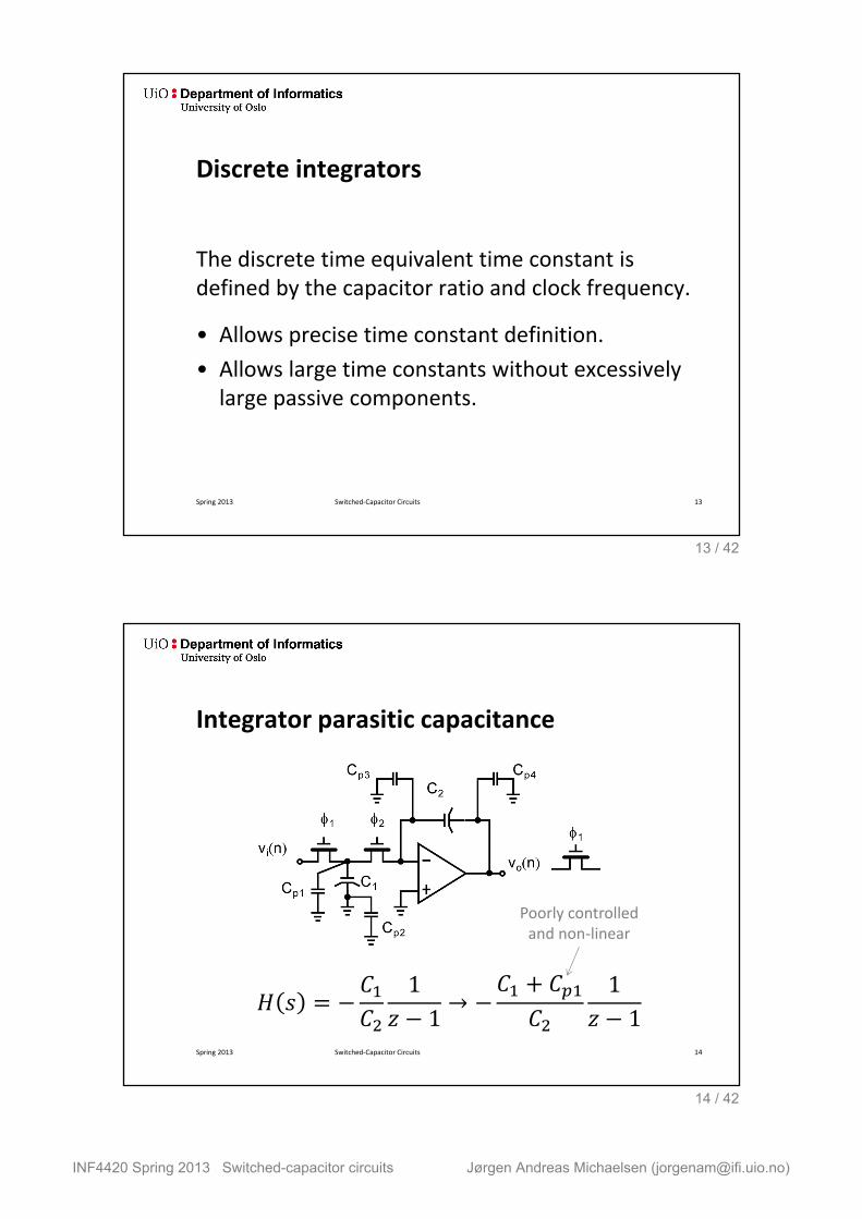
Discrete integrators
The discrete time equivalent time constant is defined by the capacitor ratio and clock frequency.
• Allows precise time constant definition.
• Allows large time constants without excessively large passive components.
Spring 2013 Switched-Capacitor Circuits 13
13 / 42
Integrator parasitic capacitance
𝐻 𝑠 = −𝐶1
𝐶2
1
𝑧 − 1→ −
𝐶1 + 𝐶𝑝1
𝐶2
1
𝑧 − 1
Spring 2013 Switched-Capacitor Circuits 14
Poorly controlled and non-linear
14 / 42
INF4420 Spring 2013 Switched-capacitor circuits Jørgen Andreas Michaelsen ([email protected])
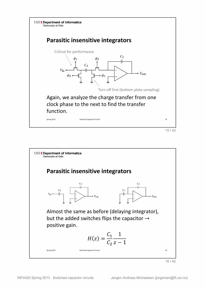
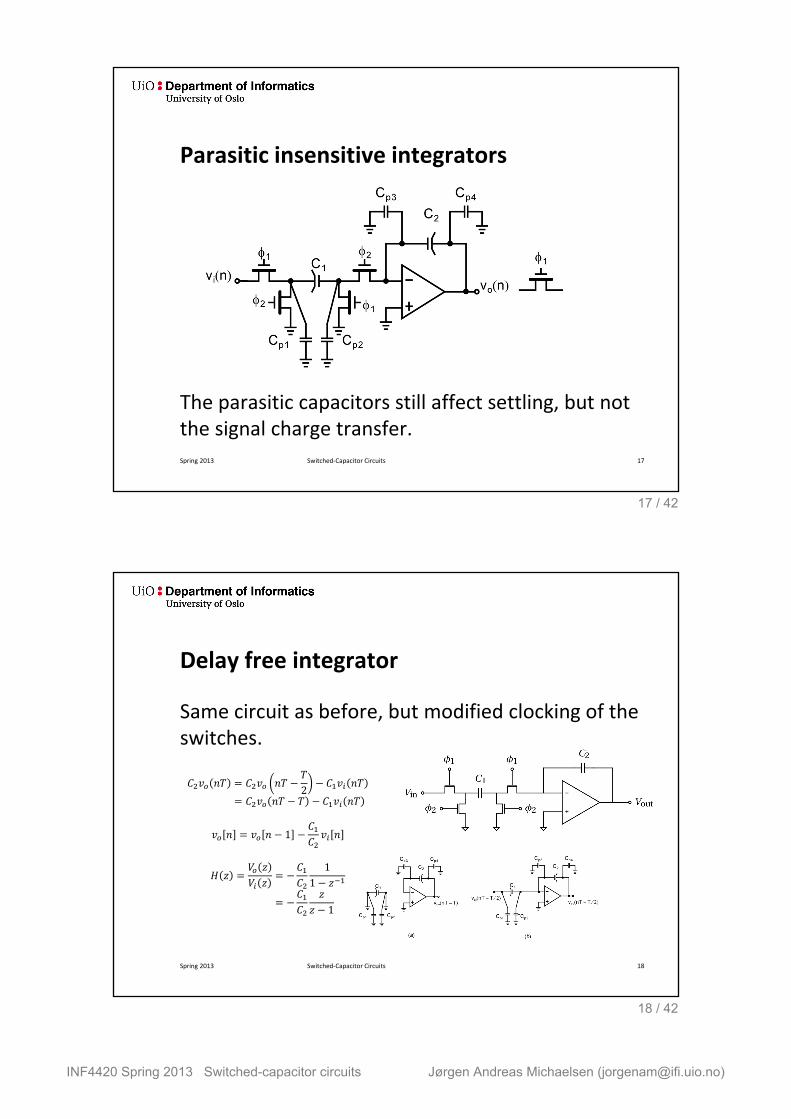
Parasitic insensitive integrators
Again, we analyze the charge transfer from one clock phase to the next to find the transfer function.
Spring 2013 Switched-Capacitor Circuits 15
Critical for performance
Turn off first (bottom plate sampling)
15 / 42
Parasitic insensitive integrators
Almost the same as before (delaying integrator), but the added switches flips the capacitor → positive gain.
𝐻 𝑧 =𝐶1
𝐶2
1
𝑧 − 1
Spring 2013 Switched-Capacitor Circuits 16
16 / 42
INF4420 Spring 2013 Switched-capacitor circuits Jørgen Andreas Michaelsen ([email protected])
Parasitic insensitive integrators
The parasitic capacitors still affect settling, but not the signal charge transfer.
Spring 2013 Switched-Capacitor Circuits 17
17 / 42
Delay free integrator
Same circuit as before, but modified clocking of the switches.
Spring 2013 Switched-Capacitor Circuits 18
𝐶2𝑣𝑜 𝑛𝑇 = 𝐶2𝑣𝑜 𝑛𝑇 −𝑇
2− 𝐶1𝑣𝑖 𝑛𝑇
= 𝐶2𝑣𝑜 𝑛𝑇 − 𝑇 − 𝐶1𝑣𝑖 𝑛𝑇
𝑣𝑜 𝑛 = 𝑣𝑜 𝑛 − 1 −𝐶1
𝐶2𝑣𝑖 𝑛
𝐻 𝑧 =𝑉𝑜 𝑧
𝑉𝑖 𝑧= −
𝐶1
𝐶2
1
1 − 𝑧−1
= −𝐶1
𝐶2
𝑧
𝑧 − 1
18 / 42

INF4420 Spring 2013 Switched-capacitor circuits Jørgen Andreas Michaelsen ([email protected])
Signal flow graph analysis
• Now we have the fundamental building blocks (discrete time integrators), to realize filters.
• We need a more convenient tool to analyze large systems.
• Signal flow graph (SFG) analysis allows us to graphically analyze SC systems.
Spring 2013 Switched-Capacitor Circuits 19
19 / 42
Signal flow graph analysis
Spring 2013 Switched-Capacitor Circuits 20
𝐻1 𝑧 =𝑉𝑜 𝑧
𝑉1 𝑧= −
𝐶1
𝐶𝐴
(inverting gain stage) 𝐻2(𝑧) is the non-inverting delaying integrator 𝐻3(𝑧) is the inverting delay-free integrator
20 / 42

INF4420 Spring 2013 Switched-capacitor circuits Jørgen Andreas Michaelsen ([email protected])
SC filters
A simple design strategy:
• Start with a continuous time prototype
• Replace resistors with SC resistor equivalents
The resulting circuit is similar for input frequencies much lower than the sampling frequency
• Use SFG to determine the z-domain transfer function
Accurate description of the transfer function
Spring 2013 Switched-Capacitor Circuits 21
21 / 42
First order filters
Filter design example.
Start with the continuous time circuit. In this case:
Spring 2013 Switched-Capacitor Circuits 22
22 / 42

INF4420 Spring 2013 Switched-capacitor circuits Jørgen Andreas Michaelsen ([email protected])
First order filters
Replace the resistors with SC elements
Spring 2013 Switched-Capacitor Circuits 23
23 / 42
First order filters
• Use Fig. 14.14 to find the SFG
• From this we find the z-domain transfer function
• 𝐻 𝑧 = −1
𝐶𝐴
𝐶2+𝐶1 1−𝑧−1
1+𝐶3𝐶𝐴
−𝑧−1
• Find pole and zero (stability)
• Frequency response, 𝑧 = 𝑒𝑗𝜔𝑇 ≈ 1 + 𝑗𝜔𝑇
Spring 2013 Switched-Capacitor Circuits 24
24 / 42

INF4420 Spring 2013 Switched-capacitor circuits Jørgen Andreas Michaelsen ([email protected])
Switch sharing
Some switches are redundant, we use this to simplify the circuit:
Spring 2013 Switched-Capacitor Circuits 25
25 / 42
Biquad filters
Ratio of two quadratic functions. In continuous time
𝐻 𝑠 = −𝑘2𝑠2 + 𝑘1𝑠 + 𝑘0
𝑠2 +𝜔0𝑄
𝑠 + 𝜔02
Spring 2013 Switched-Capacitor Circuits 26
26 / 42

INF4420 Spring 2013 Switched-capacitor circuits Jørgen Andreas Michaelsen ([email protected])
Low-Q biquad
Spring 2013 Switched-Capacitor Circuits 27
27 / 42
Low-Q biquad
𝐻 𝑧 = −𝐾2 + 𝐾3 𝑧2 + 𝐾1𝐾5 − 𝐾2 − 2𝐾3 𝑧 + 𝐾3
1 + 𝐾6 𝑧2 + 𝐾4𝐾5 − 𝐾6 − 2 𝑧 + 1
Spring 2013 Switched-Capacitor Circuits 28
28 / 42

INF4420 Spring 2013 Switched-capacitor circuits Jørgen Andreas Michaelsen ([email protected])
Low-Q biquad
• A design strategy for determining capacitor sizing is outlined in the book
• High-Q transfer functions result in large capacitor spread (ratio of the smallest and largest capacitor)
• As before, we find the frequency response as
𝐻 𝑒𝑗𝜔𝑇
Spring 2013 Switched-Capacitor Circuits 29
29 / 42
High-Q biquad
Spring 2013 Switched-Capacitor Circuits 30
30 / 42

INF4420 Spring 2013 Switched-capacitor circuits Jørgen Andreas Michaelsen ([email protected])
High-Q biquad
𝐻 𝑧 = −𝐾3𝑧2 + 𝐾1𝐾5 + 𝐾2𝐾5 − 2𝐾3 𝑧 + 𝐾3 − 𝐾2𝐾5
𝑧2 + 𝐾4𝐾5 + 𝐾5𝐾6 − 2 𝑧 + 1 − 𝐾5𝐾6
This transfer function turns out to be better suited for realizing high-Q transfer functions (less spread).
Spring 2013 Switched-Capacitor Circuits 31
31 / 42
Gain
• Resettable gain circuit
• Samples offset voltage during reset (reduces flicker noise)
Spring 2013 Switched-Capacitor Circuits 32
32 / 42

INF4420 Spring 2013 Switched-capacitor circuits Jørgen Andreas Michaelsen ([email protected])
Gain
Amplifier slew-rate requirement is high.
Spring 2013 Switched-Capacitor Circuits 33
33 / 42
Capacitive-reset gain
Include a capacitor to hold the output during the reset phase. Avoid excessive slewing. Configurable positive or negative gain.
Spring 2013 Switched-Capacitor Circuits 34
34 / 42

INF4420 Spring 2013 Switched-capacitor circuits Jørgen Andreas Michaelsen ([email protected])
Noise
Noise from the switch is sampled on the capacitor with the signal.
Sampling the 𝑘𝑇
𝐶 noise is like sampling any other
signal. The total noise power remains. Broadband noise alias back to the signal band.
Spring 2013 Switched-Capacitor Circuits 35
35 / 42
Noise
In the delaying parasitic insensitive case, noise is sampled independently in 𝜙1 and 𝜙2, doubling the
noise: 2𝑘𝑇
𝐶
Spring 2013 Switched-Capacitor Circuits 36
36 / 42

INF4420 Spring 2013 Switched-capacitor circuits Jørgen Andreas Michaelsen ([email protected])
Correlated double sampling (CDS)
• We have already seen how opamp offset voltage can be sampled and canceled.
• Generally, this technique is known as correlated double sampling (CDS)
• Flicker noise is low frequency (assumed to be occurring at lower frequencies than the sampling frequency). Can model it as a randomly varying offset voltage → also canceled
• Can be applied to different sampled systems Spring 2013 Switched-Capacitor Circuits 37
37 / 42
Fully differential circuits
Real circuits are almost always fully differential. Coupled noise, power supply noise, substrate noise will mostly affect the common mode, while our signal is in the differential mode. Also, cancels even order harmonics.
Spring 2013 Switched-Capacitor Circuits 38
38 / 42

INF4420 Spring 2013 Switched-capacitor circuits Jørgen Andreas Michaelsen ([email protected])
Charge injection
We discussed performance limitation of the switches in the context of sample and hold circuits. The same applies for SC. As we have seen, charge injection limits linearity.
→ arrange the switching and clocking to minimize the signal dependent charge injection.
Spring 2013 Switched-Capacitor Circuits 39
39 / 42
Bootstrapped switch
Generate a clock voltage such that 𝑉𝐺𝑆 is constant (𝑉𝑖𝑛 + 𝑉𝑑𝑑). Better 𝑅𝑜𝑛 and alleviates charge injection problem. Increased complexity, and reliability can be problematic.
Spring 2013 Switched-Capacitor Circuits 40
40 / 42

INF4420 Spring 2013 Switched-capacitor circuits Jørgen Andreas Michaelsen ([email protected])
SC amplifier design
Unanswered questions (for now). How do we design amplifiers suitable for SC circuits?
• DC gain (static error)
• GBW (dynamic error)
• PM (stability)
• Slewing requirements
• 𝐶𝑖𝑛 (capacitive divider)
• … Spring 2013 Switched-Capacitor Circuits 41
41 / 42
Further reading
Sansen, Analog Design Essentials, Springer, 2006, Ch. 17
Spring 2013 Switched-Capacitor Circuits 42
42 / 42