Embed Size (px)
Citation preview
HAL Id: hal-01738024https://hal.archives-ouvertes.fr/hal-01738024
Submitted on 11 Jul 2018
HAL is a multi-disciplinary open accessarchive for the deposit and dissemination of sci-entific research documents, whether they are pub-lished or not. The documents may come fromteaching and research institutions in France orabroad, or from public or private research centers.
L’archive ouverte pluridisciplinaire HAL, estdestinée au dépôt et à la diffusion de documentsscientifiques de niveau recherche, publiés ou non,émanant des établissements d’enseignement et derecherche français ou étrangers, des laboratoirespublics ou privés.
Optoelectrical modeling of solar cells based onc-Si/a-Si:H nanowire arrays: focus on the electrical
transport in between the nanowiresAlexandra Levtchenko, Sylvain Le Gall, Raphaël Lachaume, Jérôme
Michallon, Stéphane Collin, José Alvarez, Zakaria Djebbour, Jean-PaulKleider
To cite this version:Alexandra Levtchenko, Sylvain Le Gall, Raphaël Lachaume, Jérôme Michallon, Stéphane Collin, etal.. Optoelectrical modeling of solar cells based on c-Si/a-Si:H nanowire arrays: focus on the electricaltransport in between the nanowires. Nanotechnology, Institute of Physics, 2018, nanotechnology, 29(25), pp.255401. �10.1088/1361-6528/aab7e8�. �hal-01738024�
Nanotechnology
ACCEPTED MANUSCRIPT
Optoelectrical modeling of solar cells based on c-Si/a-Si:H nanowirearrays: focus on the electrical transport in between the nanowiresTo cite this article before publication: Alexandra Levtchenko et al 2018 Nanotechnology in press https://doi.org/10.1088/1361-6528/aab7e8
Manuscript version: Accepted Manuscript
Accepted Manuscript is “the version of the article accepted for publication including all changes made as a result of the peer review process,and which may also include the addition to the article by IOP Publishing of a header, an article ID, a cover sheet and/or an ‘AcceptedManuscript’ watermark, but excluding any other editing, typesetting or other changes made by IOP Publishing and/or its licensors”
This Accepted Manuscript is © 2018 IOP Publishing Ltd.
During the embargo period (the 12 month period from the publication of the Version of Record of this article), the Accepted Manuscript is fullyprotected by copyright and cannot be reused or reposted elsewhere.As the Version of Record of this article is going to be / has been published on a subscription basis, this Accepted Manuscript is available for reuseunder a CC BY-NC-ND 3.0 licence after the 12 month embargo period.
After the embargo period, everyone is permitted to use copy and redistribute this article for non-commercial purposes only, provided that theyadhere to all the terms of the licence https://creativecommons.org/licences/by-nc-nd/3.0
Although reasonable endeavours have been taken to obtain all necessary permissions from third parties to include their copyrighted contentwithin this article, their full citation and copyright line may not be present in this Accepted Manuscript version. Before using any content from thisarticle, please refer to the Version of Record on IOPscience once published for full citation and copyright details, as permissions will likely berequired. All third party content is fully copyright protected, unless specifically stated otherwise in the figure caption in the Version of Record.
View the article online for updates and enhancements.
This content was downloaded from IP address 129.175.97.14 on 20/03/2018 at 08:53

Optoelectrical modeling of solar cells based on c-Si/a-Si:H
nanowire arrays: focus on the electrical transport in between the
nanowires
Alexandra Levtchenko1, Sylvain Le Gall1*, Raphaël Lachaume1,2, Jérôme Michallon1,2,3, Stéphane Collin3, José Alvarez1, Zakaria Djebbour1†, and Jean-Paul Kleider1
1 Génie électrique et électronique de Paris, UMR CNRS 8507, CentraleSupélec, Univ. Paris-Sud, UPMC, 11 rue Joliot-Curie, Plateau de Moulon 91192 Gif-sur-Yvette, France
2 Institut Photovoltaïque d’Ile-de-France, 8 rue de la Renaissance, 92160 Antony, France 3 Centre de Nanosciences et de Nanotechnologies, CNRS, Univ. Paris-Sud, C2N – Marcoussis, 91460
Marcoussis, France †Département des Sciences Physiques, UVSQ, 45 av des Etats-Unis, 78035 Versailles, France
By coupling optical and electrical modeling, we have investigated the photovoltaic performances
of p-i-n radial nanowires array based on crystalline p-type silicon (c-Si) core/hydrogenated
amorphous silicon (a-Si:H) shell. By varying either the doping concentration of the c-Si core, or back
contact work function we can separate and highlight the contribution to the cell’s performance of the
nanowires themselves (the radial cell) from the interspace between the nanowires (the planar cell).
We show that the build-in potential (Vbi) in the radial and planar cells strongly depends on the doping
of c-Si core and the work function of the back contact respectively. Consequently, the solar cell’s
performance is degraded if either the doping concentration of the c-Si core, or/and the work function
of the back contact is too low. By inserting a thin (p) a-Si:H layer between both core/absorber and
back contact/absorber, the performance of the solar cell can be improved by partly fixing the Vbi at
both interfaces due to strong electrostatic screening effect. Depositing such a buffer layer playing the
role of an electrostatic screen for charge carriers is a suggested way of enhancing the performance of
solar cells based on radial p-i-n or n-i-p nanowire array.
* Corresponding author: [email protected]
Page 1 of 12 AUTHOR SUBMITTED MANUSCRIPT - NANO-116527.R1
123456789101112131415161718192021222324252627282930313233343536373839404142434445464748495051525354555657585960 A
ccep
ted
Man
uscr
ipt

1. Introduction
Semiconductor nanowires have attracted much attention in the last decade for their unique
electronic properties and potential applications in several emerging areas such as electronic sensor,
photovoltaic, thermoelectric, battery and biological applications [1]. Especially, silicon nanowires are
under active investigation for photovoltaic applications because they offer novel approaches for solar
to electric energy conversion leading to high-efficiency devices by simple manufacturing [2-4]. Due to
their geometry, silicon nanowires provide excellent anti-reflection and light trapping effects [5, 6],
which make this array of nanowires a promising candidate to lower both the required quality and
quantity of silicon material. Moreover, radial p-n junctions obtained with the cylindrical structure
allow to decouple light absorption along the wire axis and the carrier collection along the radial
direction. Among other nanowire technologies, crystalline silicon (c-Si) nanowire based solar cells
have been emerging [7] with high power conversion efficiency [8-10]. However, the technology based
on crystalline silicon is an expensive mainly due to the manufacturing costs of processing,
crystallization, purification etc. A good alternative for low cost solar cells is to use of the thin film
technologies such as hydrogenated amorphous silicon (a-Si:H). In this regard, significant
improvements in nanowire growth and material properties can be obtained by considering a c-Si core
nanowires surrounded by an a-Si:H absorber shell forming a radial p-i-n heterojunctions [11-13].
Numerical simulations have revealed to be powerful tools to guide the ideal design of radial
heterojunctions considered in nanowire based solar cells. For instance, optical modeling has been used
to investigate the optical light harvesting properties [11, 14-16], while electrical modeling has been
used to determine their electrical performance, but without taking into account the light enhancement
effects due to nanostructuration [17, 18]. Very few articles rigorously take into account both the
optical and electrical aspects [19]. Recently, we have developed a tool to couple electrical and optical
simulators and we applied it on p-i-n radial nanowires based on c-Si core/a-Si:H shell heterojunction
in order to simulate the electrical performance of solar cells when the light harvesting effect is taken
into account in the photogeneration rate distribution of vertical nanowire arrays [20]. It was
emphasized that the planar region between the nanowires has to be taken into account because it
strongly influences the performance of the entire solar cell. In this study, we perform coupled
optical/electrical modeling on the same structure, and show that the performance of the solar cell can
be increased by inserting a thin (p) a-Si:H buffer layer in the stack.
2. Structure and modeling
The structure of interest is depicted in figures 1(a) and 1(b), and is similar to the one studied in our
previous work [20]. The array of nanowires has been designed from experimental achievements [11-
13]. For the modeling, a periodic square mesh arrangement was considered with a nanowire density of
2.6 ×108 cm-2 roughly equivalent to a period of 620 nm [12, 20]. Each nanowire, described in figure
1(b), consists in a radial p-i-n junction with 20 nm p-type crystalline silicon core, (p)c-Si, covered by
100 nm of intrinsic hydrogenated amorphous silicon absorber, (i)a-Si:H, surrounded by 10 nm of n-
type hydrogenated amorphous silicon shell, (n)a-Si:H. The 1 µm long c-Si core allows the radial
collection of holes which then flow to the back contact made of aluminium-doped zinc oxide (AZO).
Radial collection of electrons is ensured by indium tin oxide (ITO). In addition to the radial junction
for nanowires, the solar cell also integrates the planar junction in between the nanowires.
The electrical modeling was performed using TCAD software (ATLAS from Silvaco [21]) based
on the finite volume method, which solves the physical equations self-consistently: Poisson and carrier
continuity equations with the drift-diffusion transport. The mesh was reduced and refined close to the
interfaces until a stable solution was obtained. Electrical parameters of the different semiconductor
materials are gathered in Table 1. Amorphous silicon was modeled with a density of states (DOS) in
the bandgap, consisting of two exponential tail state distributions (acceptor-like for the conduction
band tail and donor-like for the valence band tail) and two Gaussian deep defect distributions
representative of dangling bonds (one donor-type and the other acceptor-type). According to the
Page 2 of 12AUTHOR SUBMITTED MANUSCRIPT - NANO-116527.R1
123456789101112131415161718192021222324252627282930313233343536373839404142434445464748495051525354555657585960 A
ccep
ted
Man
uscr
ipt
defect-pool model, the equilibrium DOS in a-Si:H depends on the position of the Fermi level [22],
meaning that it should be non-homogeneous especially close to the core and the outer shell interfaces.
However we checked that the changes in the DOS close to the interfaces did not have strong impact on
the presented results and on the trends observed when varying the doping density in the c-Si core or
the AZO work function. The input parameters for the DOS of the a-Si:H layers are reported in Table 2.
More details about the electrical parameters of a-Si:H layers can be found elsewhere [20]. In the (p)c-
Si core, recombination using both standard Shockley–Read–Hall and Auger models were taken into
account and the electron and hole mobilities were also considered as doping dependent using a
standard model [23, 24]. The work function of ITO was chosen to meet flat band conditions at the
ITO/(n) a-Si:H interface in order to study only the influence of the AZO contact. The work function
values of transparent conductive oxides (TCO) such as AZO depend on the measurement technique as
well as on the material synthesis conditions [25, 26], therefore in this study it was varied by ±0.5 eV
around 5 eV. Interfaces between the different layers were considered as ideal (no interface defects).
The surface recombination velocities at the contacts were taken infinite for both types of carriers (no
selective contacts for collection) [27].
Optical modeling was performed using a three-dimensional Rigorous Coupled Wave Analysis
(RCWA) method in order to calculate the carrier photogeneration in the nanowire array. The optical
indices of materials were directly extracted from ellipsometry measurements. In contrast with the
electrical simulation where ITO and AZO are replaced by electric contact modelled by specific
boundary conditions (work function and surface recombination velocities values), the optical
simulation considers the bulk of both ITO and AZO materials (with optical indices). Photogeneration
profile of a single nanowire extracted from optical simulation is then flattened to a 2D plane to be
input in the electrical simulations [19, 20, 28, 29]. The photogeneration profile is shown in figure 1(c).
As expected, this profile is different from the exponentially decreasing profile from the illuminated
surface, as would be obtained from the simple Beer-Lambert absorption law. To realize the
optical/electrical coupling, this photogeneration profile is then implemented into the TCAD simulator
that exploits the radial symmetry of the nanowires. More details about the electrical and optical
modeling and coupling can be found in our previous paper [20].
As shown in figures 1(a), 1(b) and 1(c), the studied structure is composed of two parts: a radial p-i-
n cell in the nanowire and a planar p-i-n cell related to the interspacing in between the nanowires. The
impact of each part on the performance of the entire solar cell is investigated by varying the doping of
the p-type c-Si core and the back contact work function of AZO (WAZO) as they determine the band-
bending in the (i) a-Si:H absorber in the radial and planar part, respectively.
3. Results and discussion
The one-dimensional energy band diagrams at equilibrium computed along the cutline as defined
in figure 2(a) for the radial and planar junctions are shown in figure 2 (b) and 2(c), respectively. For
the radial junction, the band-bending is strongly impacted by the acceptor concentration (Na) of the c-
Si core. Indeed, the built-in potential (Vbi) increases, for instance, from 0.28 eV for Na=1×1018 cm-3 to
1.05 eV for Na=8×1018 cm-3 (figure 2(b)). The strong decrease of Vbi is not only related to the decrease
of the doping core Na but is also impacted by the thickness of the c-Si core because it limits the width
of the space charge region (the number of acceptor charges is too low in the c-Si core with a radius of
20 nm). However, by increasing the c-Si core radius above ~100 nm, additional simulations (not
shown) indicated that the Vbi follows the variation of the c-Si work function according to the doping
concentration.
For the planar junction, Vbi in the absorber increases with increasing the AZO work function
(WAZO), as reported in figure 2(c). The change of the band-bending according to either Na or WAZO,
and the competition between them, impact directly the photovoltaic performance of the entire solar
cell. The evolution of the short-circuit current density (Jsc), open-circuit voltage (Voc) and efficiency,
for varying the doping of c-Si and WAZO, are shown in figure 2 (d), 2(e) and 2(f) respectively. The
Page 3 of 12 AUTHOR SUBMITTED MANUSCRIPT - NANO-116527.R1
123456789101112131415161718192021222324252627282930313233343536373839404142434445464748495051525354555657585960 A
ccep
ted
Man
uscr
ipt
strong dependence of Jsc with the doping concentration of the c-Si core is due to the increase of Vbi in
the absorber in the radial part, which increases the electric field and improves the charge carrier
separation. An increase of Vbi also takes place in the absorber in the planar part by increasing the
WAZO. However, as the photogeneration rate is lower in the planar part in between the nanowire than
in the nanowire, the carrier collection enhancement by the electric field has a weaker effect here,
which explains the low WAZO dependence of Jsc in the entire cell. So, this explains why Jsc is mainly
influenced by the radial cell.
In figure 2(e), two behaviours can be distinguished for the evolution of Voc. For WAZO<5.0 eV, the
Voc increases linearly with WAZO, independently of Na values. The strong impact of WAZO on Voc is due
to the increase of Vbi in the absorber in the planar region, meaning that Voc is mainly influenced by the
planar cell. On the contrary, for WAZO > 5.0 eV, Vbi of the absorber is lower in the radial junction as
compared to the planar one, leading to Na dependence of Voc. Indeed, the increase of WAZO leads to a
decrease of the dark current density mainly driven by the planar region [20], which explains the drop
in Voc. Thus, for low WAZO values, Voc of the entire cell is degraded due to the planar region.
The efficiency values in figure 2(f) are driven by the evolution of Voc. So it appears that the planar
junction can drastically affect the performance of the solar cell, mainly for lowly doped c-Si core and
AZO back contact having a low work function value.
In order to remove the dependence of the core doping and back contact work function on the solar
cell efficiency, a thin buffer layer of p-type a-Si:H at the AZO/absorber interface (and also at the
core/absorber interface) as depicted in figure 3(a), is now investigated. This buffer layer is modeled by
a 10 nm thick (p) a-Si:H with input electrical parameters reported in Table 1 and the DOS from Table
2. To keep the same thickness of 100 nm for the absorber layer as for the reference structure, the
thickness of the (i) a-Si:H layer is thus reduced to 90 nm.
The one-dimensional energy band diagrams at equilibrium for the radial and planar junctions for
the new structure are shown in figure 3 (b) and 3(c) respectively at the exact same position as
compared to the reference structure (figures 2(b) and 2(c)). For the radial junction, we notice that the
band-bending is not influenced by Na values. Contrary to the reference structure without (p) a-Si:H
layer, Vbi is fixed by the pinning of the Fermi level in the (p) a-Si:H layer i.e Vbi is fixed due to the
electrostatic screening effect provided by the numerous charged defects of the inserted highly doped
(p) a-Si:H layer [27]. Indeed, we can estimate the Debye screening length LD=(ε/q²N(EF))1/2 around 4.5
nm in this (p) a-Si/H buffer layer (here N(EF)~3×1019 cm-3 is the DOS at Fermi level) which is good
agreement as in reference [30]. In other words, as long as this supplementary layer thickness is several
times LD, Vbi is rather not influenced by the c-Si contact work function, and nearly all the voltage drop
induced by a change of c-Si doping is taken in the (p) a-Si:H layer [26]. Similarly to the band diagram
for the planar junction of figure 3(c), the position of conduction (Ec) and valence (Ev) bands at the
border of AZO (depth of 110 nm) is fixed by the WAZO values. The inserted buffer layer increases Ec
and Ev values near the AZO metal for the lower WAZO. Consequently, a curvature in the band-bending
can appears close to the interface, as seen for instance for WAZO=4.8 eV. The maximum value of Vbi in
the absorber is thus higher in the planar junction with the additional p-type a-Si:H layer even by
electrostatic screening effect. For WAZO > 5.2 eV, this buffer layer has no impact on the band diagram
(linear bands in the absorber as in the case of the reference layer studied in figure 2(c)).
The variation of Jsc for the new structure with (p) a-Si:H buffer layer is shown in figure 3(d). We
notice that Jsc remains constant because the maximum Vbi in the absorber (so the electric field) is
independent of the doping of the c-Si core, as reveal in figure 3(b). The electric field in the absorber is
now fixed by the work function of the additional (p) a-Si:H layer. Consequently, Jsc is not anymore
Page 4 of 12AUTHOR SUBMITTED MANUSCRIPT - NANO-116527.R1
123456789101112131415161718192021222324252627282930313233343536373839404142434445464748495051525354555657585960 A
ccep
ted
Man
uscr
ipt
affected by the radial contact contrary to the structure without buffer layer. The Jsc values lie between
12.9 and 13.1 mA/cm² for WAZO in the range of 4.8-5.5 eV. These values are slightly higher than the
values (11.2-12.9 mA/cm²) of the reference structure observed previously in figure 2(d). On the other
hand, the increase of Voc as a function of WAZO is smaller than for the reference structure and reaches a
saturated value around 0.85 V, as shown in figure 3(e). The structure with the buffer layer thus
becomes less sensitive to the planar contact due to the screening effect of the (p) a-Si:H layer. This
buffer layer thus helps to increase the Voc as long as its effective work function remains higher than
WAZO. Finally, evolutions of the efficiencies are plotted in figure 3(f) for the reference (line) and the
new structure with the additional buffer layer (symbol). The efficiency is improved with the buffer
layer at low WAZO due to Voc higher. However, if WAZO is high enough to allow the major part of the
dark current to flow through the radial junction, the buffer layer will limit the solar cell performance
(if the c-Si core doping is too high).
The inserted buffer layer, due to screening effect, has a strong impact on the solar cell
performance. In the following, we have investigated the strength of the screening effect by modifying
the DOS of the (p) a-Si:H layer in the structure. In figures 4, we show the influence of the activation
energy Ea (i.e the Fermi level position from EV) of the (p) a-Si :H buffer layer on the equilibrium band-
bending. In both the radial (figure 4(a)) and planar (figure 4(b)) junctions, the maximum Vbi in the
absorber increases when Ea decreases. Basically, a lower value of Ea means a higher doped-layer (or
more defective layer) which increases the Vbi (due to increase of work function difference between the
back and front contact). In a more defective layer, LD is reduced which enhances the screening effect.
This effect is even stronger for the lowly doped core and lower WAZO. In contrast to a thin c-Si buffer
layer, the a-Si:H material develops a strong charge due to the huge DOS at the Fermi Level, so a thin
layer is enough for having a strong electrostatic screening effect.
Experimentally, S. Misra et al. (2013) [11] have deposited an additional 10 nm thick p-type a-Si:H
layer at both c-Si core/(i) a-Si:H absorber and AZO/absorber interfaces for the same p-i-n nanowire
stack. They claimed that this inserted layer allows to rise the Voc of 0.05 V, for a maximal value of
0.85 V. They explained this raise of Voc by the reduction of the recombination rate at p-i interface. In
this study, we provide another explanation: the electrostatic screening effect of this (p) a-Si:H layer.
Note that the maximum simulated Jsc (13.1 mA/cm²) and Voc (0.85 V) values are very close to that
obtained experimentally by S. Misra et al. (2013) [11].
4. Conclusion
In summary, we have investigated the performance of a radial c-Si core/a-Si:H absorber shell
nanowire array by coupling optical and electrical modeling. We show that the built-in potential Vbi of
the radial and planar junction strongly depends of the doping of c-Si core and the work function of the
AZO back contact. Consequently, the solar cell’s performance is degraded if the c-Si core is not doped
enough and the work function of the AZO back contact too low. By inserting a thin (p) a-Si:H buffer
layer in between both core/absorber and absorber/AZO interfaces, we show that Vbi in both radial and
planar junctions is mainly fixed by this buffer layer due to the strong electrostatic screening effect.
This screening effect is stronger if the thin buffer have a higher density of state in the bandgap (i.e if
the (p) a-Si:H is more defective). Consequently, the performance of the solar cell is enhanced because:
(i) the Jsc remains constant with a value higher than obtained in the structure without the buffer layer,
independently of the core doping, and (ii) the Voc increases as long as its work function remains higher
than the AZO one. The deposition of a thin defective buffer layer playing the role of electrostatic
Page 5 of 12 AUTHOR SUBMITTED MANUSCRIPT - NANO-116527.R1
123456789101112131415161718192021222324252627282930313233343536373839404142434445464748495051525354555657585960 A
ccep
ted
Man
uscr
ipt

screening for charge carriers, if the required growth both c-Si core doping and back contact quality
conditions are not fulfill, should be a cunning way to increase the solar performance of p-i-n or n-i-p
radial a-Si:H-based nanowires solar cells.
Acknowledgements
The authors acknowledge the financial support from the French Research National Agency – project
SOLARIUM (ANR-14-CE05-0025).
Page 6 of 12AUTHOR SUBMITTED MANUSCRIPT - NANO-116527.R1
123456789101112131415161718192021222324252627282930313233343536373839404142434445464748495051525354555657585960 A
ccep
ted
Man
uscr
ipt
References
[1] N. P. Dasgupta, J. Sun, C. Liu, S. Brittman, S. C. Andrews, J. Lim, H. Gao, R. Yan, and P. Yang,
Adv. Mater. 26, 2137 (2014).
[2] R. Ghosh and P. K. Giri, Nanotechnol. 28, 0120001 (2017).
[3] K.-Q. Peng and S.-T. Lee, Adv. Mater. 23, 198 (2011).
[4] F. Priolo, T. Gregorkiewicz, M. Galli and T. F. Krauss, Nat. Nanotechnology 9, 19 (2014).
[5] L. Hu and G. Chen, Nano Lett. 7, 3249 (2007)
[6] E. Garnett and P. Yang, Nano Lett. 10, 1082 (2010)
[7] T. Stelzner, M. Pietsch, G. Andra, F. Falk, E. Ose1 and S. Christiansen, Nanotechnol. 19, 295203
(2008).
[8] X. X. Lin, X. Hua, Z. G. Huang and W. Z. Shen, Nanotechnol. 24, 235402 (2013).
[9] M-D. Ko, T. Rim, K. Kim, M. Meyyappan and C-K. Baek, Sci. Rep. 5, 11646 (2015).
[10] X. X. Lin, Y. Zeng, S. H. Zhong, Z. G. Huang, H. Q. Qian, J. Ling, J. B. Zhu and W. Z. Shen,
Nanotechnol. 26, 125401 (2015).
[11] S. Misra, L. Yu, M. Foldyna, and P. Roca i Cabarrocas, IEEE Journal of Photovoltaics 5, 40
(2015).
[12] S. Misra, L. Yu, M. Foldyna, and P. Roca i Cabarrocas, Sol. Energy Mater. Sol. Cells 118, 90
(2013).
[13] S. Misra, M. Foldyna, I. Florea, L. Yu, and P. Roca i Cabarrocas, MRS Proceedings 1770, 73
(2015).
[14] L. Yu, S. Misra, J. Wang, S. Qian, M. Foldyna, J. Xu, Y. Shi, E. Johnson, and P. Roca i
Cabarrocas, Sci. Rep. 4, 4357 (2014).
[15] S. Qian, S. Misra, J. Lu, Z. Yu, L. Yu, J. Xu, J. Wang, L. Xu, Y. Shi, K. Chen, and P. Roca i
Cabarrocas, Appl. Phys. Lett. 107, 043902 (2015).
[16] H. Ferhati, F. Djeffal, D. Arar, and Z. Dibi, Phys. Status Solidi C 2017, 1700146 (2017).
[17] Z. Pei, S-T. Chang, C-W. Liu, and Y-C. Chen, IEEE Electron. Device Lett. 30, 1305 (2009).
[18] D. Diouf, I. Ngo, J-P. Kleider, M. Gueunier-Farret, and J. Alvarez, Phys. Status Solidi A 209,
1026 (2012).
[19] M. Zanuccoli, I. Semenihin, J. Michallon, E. Sangiorgi, C. Fiegna, J. Comput. Electron 12, 572
(2013)
[20] A. Levtchenko, R. Lachaume, J. Michalon, S. Collin, J. Alvarez, S. Le Gall, Z. Djebbour, and J-P.
Kleider, Phys. Status Solidi C 14, 1700181 (2017)
[21] User’s manual for ATLAS from Silvaco International.
[22] M. J. Powell and S. C. Deane, Phys. Rev. B 48, 10815 (1993).
[23] J. Dziewior, W. Schimid, Appl. Phys. Lett. 31, 349 (1977).
[24] M. E. Law, E. Solley, M. Liang, D. E. Burk, IEEE Electron. Device Lett. 12, 401 (1991).
[25] M. D. Kelzenberg, M. C. Putnam, D. B. Turner-Evans, N. S. Lewisand, H. A. Atwater, in:
Proceedings of the 34th IEEE Photovoltaic Specialists Conference (PVSC), Philadelphia, CA, USA,
2009, pp. 001948–001953.
[26] R. Lachaume, W. Favre, P. Scheiblin, X. Garros, N. Nguyen, J. Coignus, D. Munoz, G.
Reimbold, Energy Procedia 38, 770 (2013).
[27] R. Lachaume thesis “Contribution to the electrical characterization and to the numerical
simulatio,n of the silicon heterojunction solar cells », PhD Thesis (French) 2014, Grenoble Univ.,
https://tel.archives-ouvertes.fr/tel-01186474.
[28] R. Jaramillo, and S. Ramanathan, Sol. Energ.Mater. Sol. Cells 95, 602, 2011.
[29] J. Michallon, D. Bucci, A. Morand, M. Zanuccoli, V. Consonni, A. Kaminski-Cachopo, Opt.
Express 22, A1174 (2014)
[30] R. Varache, J-P. Kleider, W. Favre, L. Korte, J. Appl. Phys. 112, 123717 (2012)
Page 7 of 12 AUTHOR SUBMITTED MANUSCRIPT - NANO-116527.R1
123456789101112131415161718192021222324252627282930313233343536373839404142434445464748495051525354555657585960 A
ccep
ted
Man
uscr
ipt
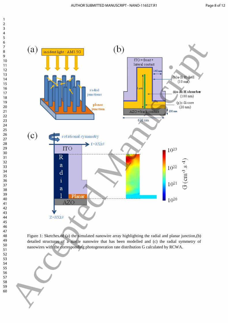
Figure 1: Sketches of (a) the simulated nanowire array highlighting the radial and planar junction,(b)
detailed structures of a single nanowire that has been modelled and (c) the radial symmetry of
nanowires with the corresponding photogeneration rate distribution G calculated by RCWA.
Page 8 of 12AUTHOR SUBMITTED MANUSCRIPT - NANO-116527.R1
123456789101112131415161718192021222324252627282930313233343536373839404142434445464748495051525354555657585960 A
ccep
ted
Man
uscr
ipt
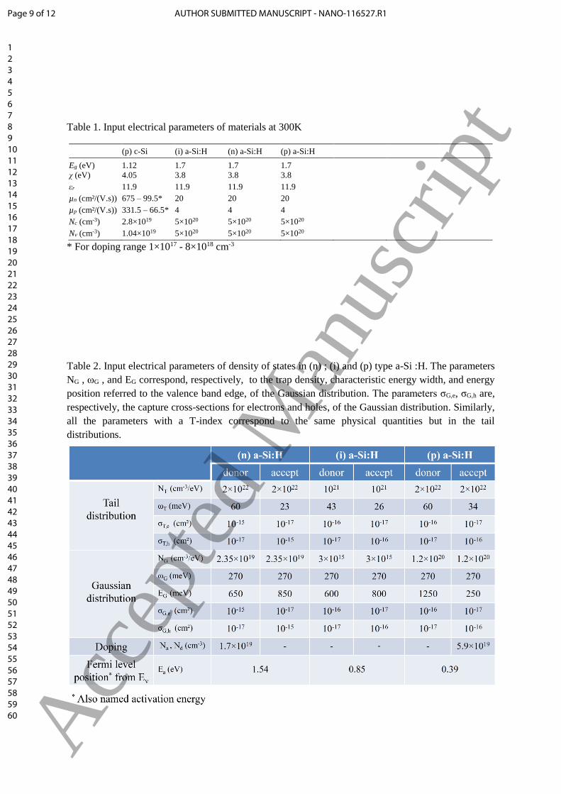
Table 1. Input electrical parameters of materials at 300K
(p) c-Si (i) a-Si:H (n) a-Si:H (p) a-Si:H
Eg (eV) 1.12 1.7 1.7 1.7
χ (eV) 4.05 3.8 3.8 3.8
εr 11.9 11.9 11.9 11.9
µn (cm²/(V.s)) 675 – 99.5* 20 20 20
µp (cm²/(V.s)) 331.5 – 66.5* 4 4 4
Nc (cm-3) 2.8×10¹⁹ 5×10²⁰ 5×10²⁰ 5×10²⁰
Nv (cm-3) 1.04×10¹⁹ 5×10²⁰ 5×10²⁰ 5×10²⁰
* For doping range 1×10¹⁷ - 8×1018 cm-3
Table 2. Input electrical parameters of density of states in (n) ; (i) and (p) type a-Si :H. The parameters
NG , ωG , and EG correspond, respectively, to the trap density, characteristic energy width, and energy
position referred to the valence band edge, of the Gaussian distribution. The parameters σG,e, σG,h are,
respectively, the capture cross-sections for electrons and holes, of the Gaussian distribution. Similarly,
all the parameters with a T-index correspond to the same physical quantities but in the tail
distributions.
Page 9 of 12 AUTHOR SUBMITTED MANUSCRIPT - NANO-116527.R1
123456789101112131415161718192021222324252627282930313233343536373839404142434445464748495051525354555657585960 A
ccep
ted
Man
uscr
ipt
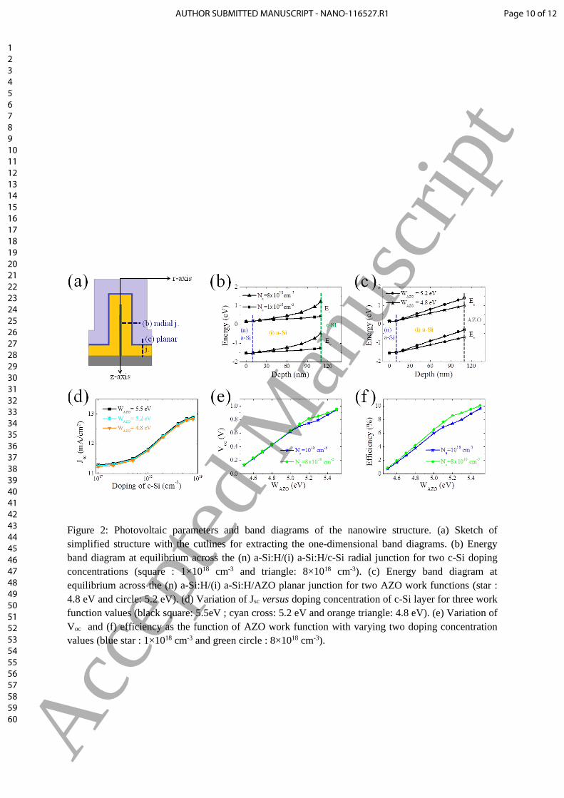
Figure 2: Photovoltaic parameters and band diagrams of the nanowire structure. (a) Sketch of
simplified structure with the cutlines for extracting the one-dimensional band diagrams. (b) Energy
band diagram at equilibrium across the (n) a-Si:H/(i) a-Si:H/c-Si radial junction for two c-Si doping
concentrations (square : 1×1018 cm-3 and triangle: 8×1018 cm-3). (c) Energy band diagram at
equilibrium across the (n) a-Si:H/(i) a-Si:H/AZO planar junction for two AZO work functions (star :
4.8 eV and circle: 5.2 eV). (d) Variation of Jsc versus doping concentration of c-Si layer for three work
function values (black square: 5.5eV ; cyan cross: 5.2 eV and orange triangle: 4.8 eV). (e) Variation of
Voc and (f) efficiency as the function of AZO work function with varying two doping concentration
values (blue star : 1×1018 cm-3 and green circle : 8×1018 cm-3).
Page 10 of 12AUTHOR SUBMITTED MANUSCRIPT - NANO-116527.R1
123456789101112131415161718192021222324252627282930313233343536373839404142434445464748495051525354555657585960 A
ccep
ted
Man
uscr
ipt
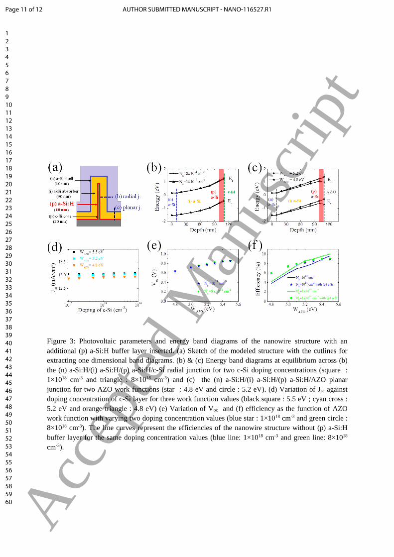
Figure 3: Photovoltaic parameters and energy band diagrams of the nanowire structure with an
additional (p) a-Si:H buffer layer inserted. (a) Sketch of the modeled structure with the cutlines for
extracting one dimensional band diagrams. (b) & (c) Energy band diagrams at equilibrium across (b)
the (n) a-Si:H/(i) a-Si:H/(p) a-Si:H/c-Si radial junction for two c-Si doping concentrations (square :
1×1018 cm-3 and triangle : 8×1018 cm-3) and (c) the (n) a-Si:H/(i) a-Si:H/(p) a-Si:H/AZO planar
junction for two AZO work functions (star : 4.8 eV and circle : 5.2 eV). (d) Variation of Jsc against
doping concentration of c-Si layer for three work function values (black square : 5.5 eV ; cyan cross :
5.2 eV and orange triangle : 4.8 eV) (e) Variation of Voc and (f) efficiency as the function of AZO
work function with varying two doping concentration values (blue star : 1×1018 cm-3 and green circle :
8×1018 cm-3). The line curves represent the efficiencies of the nanowire structure without (p) a-Si:H
buffer layer for the same doping concentration values (blue line: 1×1018 cm-3 and green line: 8×10¹⁸
cm-3).
Page 11 of 12 AUTHOR SUBMITTED MANUSCRIPT - NANO-116527.R1
123456789101112131415161718192021222324252627282930313233343536373839404142434445464748495051525354555657585960 A
ccep
ted
Man
uscr
ipt
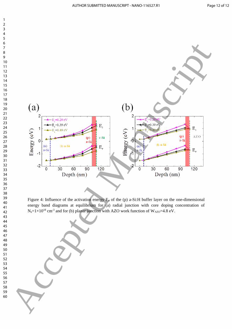
Figure 4: Influence of the activation energy Ea of the (p) a-Si:H buffer layer on the one-dimensional
energy band diagrams at equilibrium for (a) radial junction with core doping concentration of
Na=1×1018 cm-3 and for (b) planar junction with AZO work function of WAZO=4.8 eV.
Page 12 of 12AUTHOR SUBMITTED MANUSCRIPT - NANO-116527.R1
123456789101112131415161718192021222324252627282930313233343536373839404142434445464748495051525354555657585960 A
ccep
ted
Man
uscr
ipt