Embed Size (px)
Citation preview
Datasheet Rev. 1.21www.infineon.com/OPTIREG-linear 1 2021-04-20
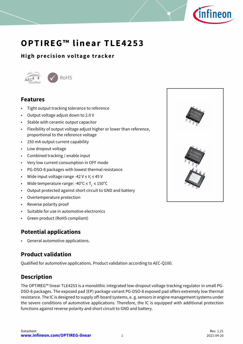
OPTIREG™ l inear TLE4253High precision voltage tracker
Features• Tight output tracking tolerance to reference• Output voltage adjust down to 2.0 V• Stable with ceramic output capacitor• Flexibility of output voltage adjust higher or lower than reference,
proportional to the reference voltage• 250 mA output current capability• Low dropout voltage• Combined tracking / enable input• Very low current consumption in OFF mode • PG-DSO-8 packages with lowest thermal resistance• Wide input voltage range -42 V ≤ VI ≤ 45 V• Wide temperature range: -40°C ≤ Tj ≤ 150°C• Output protected against short circuit to GND and battery• Overtemperature protection• Reverse polarity proof• Suitable for use in automotive electronics• Green product (RoHS compliant)
Potential applications• General automotive applications.
Product validationQualified for automotive applications. Product validation according to AEC-Q100.
DescriptionThe OPTIREG™ linear TLE4253 is a monolithic integrated low-dropout voltage tracking regulator in small PG-DSO-8 packages. The exposed pad (EP) package variant PG-DSO-8 exposed pad offers extremely low thermalresistance. The IC is designed to supply off-board systems, e. g. sensors in engine management systems underthe severe conditions of automotive applications. Therefore, the IC is equipped with additional protectionfunctions against reverse polarity and short circuit to GND and battery.
Datasheet 2 Rev. 1.21 2021-04-20
OPTIREG™ linear TLE4253High precision voltage tracker
With supply voltages up to 40 V, the output voltage follows a reference voltage applied at the adjust input withhigh accuracy. The reference voltage applied directly to the adjust input or by an e. g. external resistor dividercan be 2.0 V at minimum. The output is able to drive loads up to 250 mA at minimum while the device follows the e. g. 5 V output of amain voltage regulator acting as reference with high accuracy.The TLE4253 tracker can be set into shutdown mode in order to reduce the quiescent current to an extremelylow value. This makes the IC suitable to low power battery applications.
Type Package MarkingTLE4253GS PG-DSO-8 4253
TLE4253E PG-DSO-8 exposed pad 4253E
Datasheet 3 Rev. 1.21 2021-04-20
OPTIREG™ linear TLE4253High precision voltage tracker
Features . . . . . . . . . . . . . . . . . . . . . . . . . . . . . . . . . . . . . . . . . . . . . . . . . . . . . . . . . . . . . . . . . . . . . . . . 1
Potential applications . . . . . . . . . . . . . . . . . . . . . . . . . . . . . . . . . . . . . . . . . . . . . . . . . . . . . . . . . . . . . 1
Product validation . . . . . . . . . . . . . . . . . . . . . . . . . . . . . . . . . . . . . . . . . . . . . . . . . . . . . . . . . . . . . . . . 1
Description . . . . . . . . . . . . . . . . . . . . . . . . . . . . . . . . . . . . . . . . . . . . . . . . . . . . . . . . . . . . . . . . . . . . . . 1
Table of contents . . . . . . . . . . . . . . . . . . . . . . . . . . . . . . . . . . . . . . . . . . . . . . . . . . . . . . . . . . . . . . . . . 3
1 Block diagram . . . . . . . . . . . . . . . . . . . . . . . . . . . . . . . . . . . . . . . . . . . . . . . . . . . . . . . . . . . . . . . . . . . 4
2 Pin configuration . . . . . . . . . . . . . . . . . . . . . . . . . . . . . . . . . . . . . . . . . . . . . . . . . . . . . . . . . . . . . . . . . 52.1 Pin assignment . . . . . . . . . . . . . . . . . . . . . . . . . . . . . . . . . . . . . . . . . . . . . . . . . . . . . . . . . . . . . . . . . . . . . . . . . . . 52.2 Pin definitions and functions . . . . . . . . . . . . . . . . . . . . . . . . . . . . . . . . . . . . . . . . . . . . . . . . . . . . . . . . . . . . . . 5
3 General product characteristics . . . . . . . . . . . . . . . . . . . . . . . . . . . . . . . . . . . . . . . . . . . . . . . . . . . . 63.1 Absolute maximum ratings . . . . . . . . . . . . . . . . . . . . . . . . . . . . . . . . . . . . . . . . . . . . . . . . . . . . . . . . . . . . . . . . 63.2 Functional range . . . . . . . . . . . . . . . . . . . . . . . . . . . . . . . . . . . . . . . . . . . . . . . . . . . . . . . . . . . . . . . . . . . . . . . . . 73.3 Thermal resistance . . . . . . . . . . . . . . . . . . . . . . . . . . . . . . . . . . . . . . . . . . . . . . . . . . . . . . . . . . . . . . . . . . . . . . . 8
4 Electrical characteristics . . . . . . . . . . . . . . . . . . . . . . . . . . . . . . . . . . . . . . . . . . . . . . . . . . . . . . . . . . 94.1 Tracking regulator . . . . . . . . . . . . . . . . . . . . . . . . . . . . . . . . . . . . . . . . . . . . . . . . . . . . . . . . . . . . . . . . . . . . . . . . 94.2 Current consumption . . . . . . . . . . . . . . . . . . . . . . . . . . . . . . . . . . . . . . . . . . . . . . . . . . . . . . . . . . . . . . . . . . . . 154.3 Adjust / enable input . . . . . . . . . . . . . . . . . . . . . . . . . . . . . . . . . . . . . . . . . . . . . . . . . . . . . . . . . . . . . . . . . . . . 17
5 Application information . . . . . . . . . . . . . . . . . . . . . . . . . . . . . . . . . . . . . . . . . . . . . . . . . . . . . . . . . . 18
6 Package outlines . . . . . . . . . . . . . . . . . . . . . . . . . . . . . . . . . . . . . . . . . . . . . . . . . . . . . . . . . . . . . . . . 21
7 Revision history . . . . . . . . . . . . . . . . . . . . . . . . . . . . . . . . . . . . . . . . . . . . . . . . . . . . . . . . . . . . . . . . . 23
Table of contents
Datasheet 4 Rev. 1.21 2021-04-20
OPTIREG™ linear TLE4253High precision voltage tracker
Block diagram
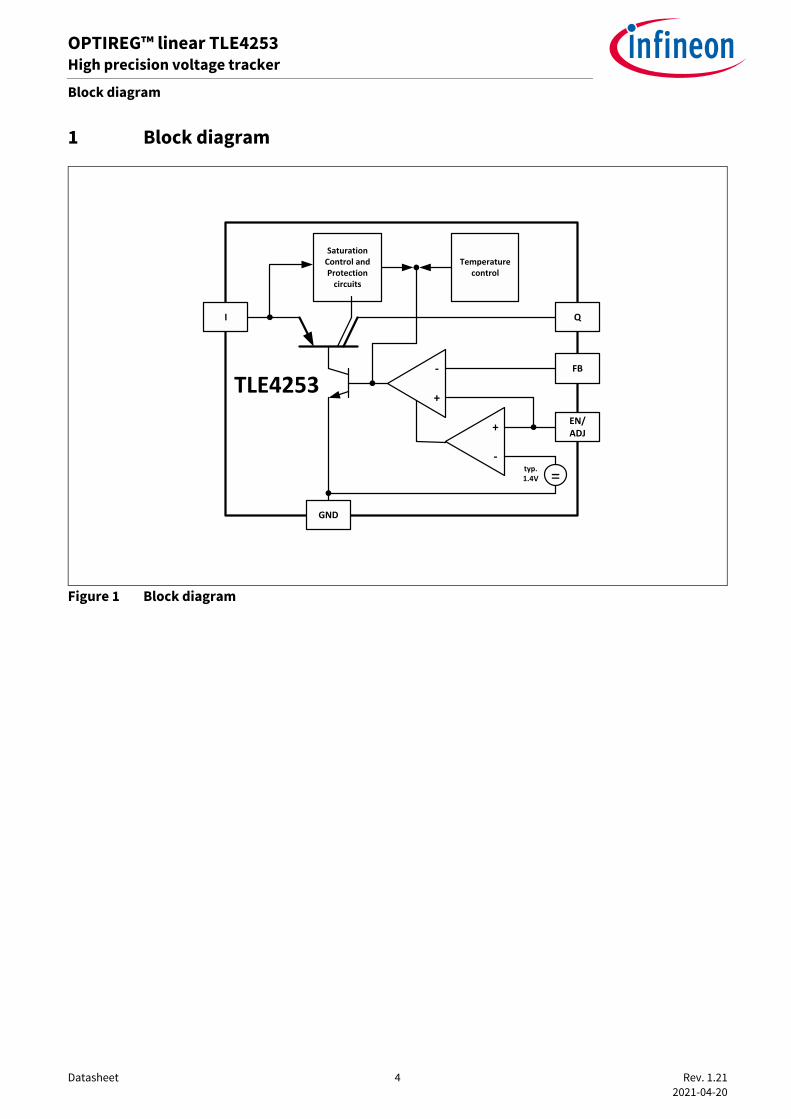
1 Block diagram
Figure 1 Block diagram
Saturation Control and Protection
circuits
Temperature control
+
-
I
GND
Q
FB
EN/ADJ
TLE4253+
-
=typ. 1.4V
Datasheet 5 Rev. 1.21 2021-04-20
OPTIREG™ linear TLE4253High precision voltage tracker
Pin configuration
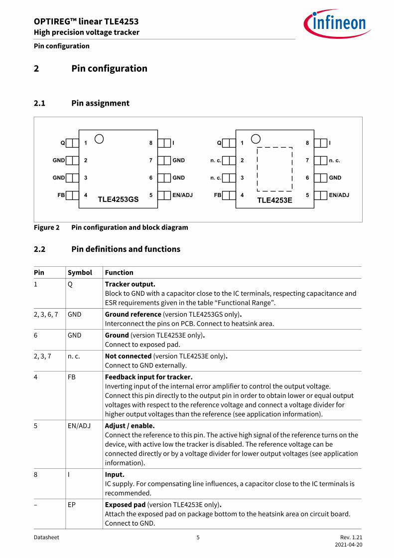
2 Pin configuration
2.1 Pin assignment
Figure 2 Pin configuration and block diagram
2.2 Pin definitions and functions
Pin Symbol Function1 Q Tracker output.
Block to GND with a capacitor close to the IC terminals, respecting capacitance and ESR requirements given in the table “Functional Range”.
2, 3, 6, 7 GND Ground reference (version TLE4253GS only).Interconnect the pins on PCB. Connect to heatsink area.
6 GND Ground (version TLE4253E only).Connect to exposed pad.
2, 3, 7 n. c. Not connected (version TLE4253E only).Connect to GND externally.
4 FB Feedback input for tracker.Inverting input of the internal error amplifier to control the output voltage.Connect this pin directly to the output pin in order to obtain lower or equal output voltages with respect to the reference voltage and connect a voltage divider for higher output voltages than the reference (see application information).
5 EN/ADJ Adjust / enable.Connect the reference to this pin. The active high signal of the reference turns on the device, with active low the tracker is disabled. The reference voltage can be connected directly or by a voltage divider for lower output voltages (see application information).
8 I Input.IC supply. For compensating line influences, a capacitor close to the IC terminals is recommended.
– EP Exposed pad (version TLE4253E only).Attach the exposed pad on package bottom to the heatsink area on circuit board. Connect to GND.
GND
GND
GND
FB EN/ADJ
IQ
4
3
2
1
TLE4253GS
GND
5
6
7
8
n. c.
n. c.
GND
FB EN/ADJ
IQ
4
3
2
1
TLE4253E
n. c.
5
6
7
8
Datasheet 6 Rev. 1.21 2021-04-20
OPTIREG™ linear TLE4253High precision voltage tracker
General product characteristics
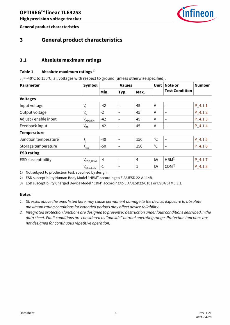
3 General product characteristics
3.1 Absolute maximum ratings
Notes1. Stresses above the ones listed here may cause permanent damage to the device. Exposure to absolute
maximum rating conditions for extended periods may affect device reliability.2. Integrated protection functions are designed to prevent IC destruction under fault conditions described in the
data sheet. Fault conditions are considered as “outside” normal operating range. Protection functions are not designed for continuous repetitive operation.
Table 1 Absolute maximum ratings 1)
Tj = -40°C to 150°C; all voltages with respect to ground (unless otherwise specified).
1) Not subject to production test, specified by design.
Parameter Symbol Values Unit Note or Test Condition
NumberMin. Typ. Max.
VoltagesInput voltage VI -42 – 45 V – P_4.1.1
Output voltage VQ -2 – 45 V – P_4.1.2
Adjust / enable input VADJ/EN -42 – 45 V – P_4.1.3
Feedback input VFB -42 – 45 V – P_4.1.4
TemperatureJunction temperature Tj -40 – 150 °C – P_4.1.5
Storage temperature Tstg -50 – 150 °C – P_4.1.6
ESD ratingESD susceptibility VESD,HBM -4 – 4 kV HBM2)
2) ESD susceptibility Human Body Model “HBM” according to EIA/JESD 22-A 114B.
P_4.1.7
VESD,CDM -1 – 1 kV CDM3)
3) ESD susceptibility Charged Device Model “CDM” according to EIA/JESD22-C101 or ESDA STM5.3.1.
P_4.1.8
Datasheet 7 Rev. 1.21 2021-04-20
OPTIREG™ linear TLE4253High precision voltage tracker
General product characteristics
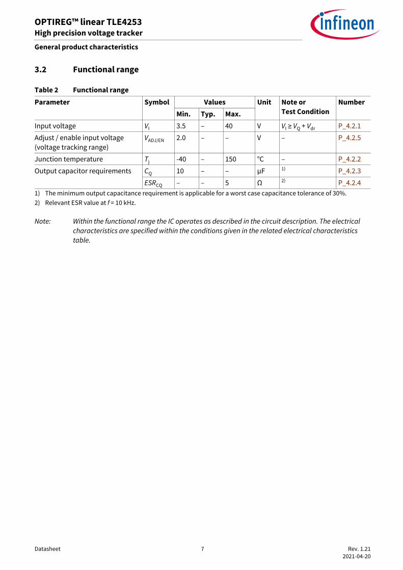
3.2 Functional range
Note: Within the functional range the IC operates as described in the circuit description. The electrical characteristics are specified within the conditions given in the related electrical characteristics table.
Table 2 Functional rangeParameter Symbol Values Unit Note or
Test ConditionNumber
Min. Typ. Max.Input voltage VI 3.5 – 40 V VI ≥ VQ + Vdr P_4.2.1
Adjust / enable input voltage (voltage tracking range)
VADJ/EN 2.0 – – V – P_4.2.5
Junction temperature Tj -40 – 150 °C – P_4.2.2
Output capacitor requirements CQ 10 – – µF 1)
1) The minimum output capacitance requirement is applicable for a worst case capacitance tolerance of 30%.
P_4.2.3
ESRCQ – – 5 Ω 2)
2) Relevant ESR value at f = 10 kHz.
P_4.2.4
Datasheet 8 Rev. 1.21 2021-04-20
OPTIREG™ linear TLE4253High precision voltage tracker
General product characteristics
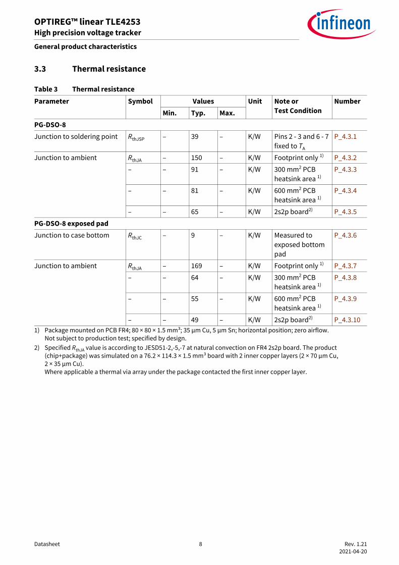
3.3 Thermal resistance
Table 3 Thermal resistanceParameter Symbol Values Unit Note or
Test ConditionNumber
Min. Typ. Max.PG-DSO-8Junction to soldering point RthJSP – 39 – K/W Pins 2 - 3 and 6 - 7
fixed to TA
P_4.3.1
Junction to ambient RthJA – 150 – K/W Footprint only 1)
1) Package mounted on PCB FR4; 80 × 80 × 1.5 mm3; 35 µm Cu, 5 µm Sn; horizontal position; zero airflow.Not subject to production test; specified by design.
P_4.3.2
– – 91 – K/W 300 mm2 PCB heatsink area 1)
P_4.3.3
– – 81 – K/W 600 mm2 PCB heatsink area 1)
P_4.3.4
– – 65 – K/W 2s2p board2)
2) Specified RthJA value is according to JESD51-2,-5,-7 at natural convection on FR4 2s2p board. The product (chip+package) was simulated on a 76.2 × 114.3 × 1.5 mm3 board with 2 inner copper layers (2 × 70 µm Cu, 2 × 35 µm Cu). Where applicable a thermal via array under the package contacted the first inner copper layer.
P_4.3.5
PG-DSO-8 exposed padJunction to case bottom RthJC – 9 – K/W Measured to
exposed bottom pad
P_4.3.6
Junction to ambient RthJA – 169 – K/W Footprint only 1) P_4.3.7
– – 64 – K/W 300 mm2 PCB heatsink area 1)
P_4.3.8
– – 55 – K/W 600 mm2 PCB heatsink area 1)
P_4.3.9
– – 49 – K/W 2s2p board2) P_4.3.10
Datasheet 9 Rev. 1.21 2021-04-20
OPTIREG™ linear TLE4253High precision voltage tracker
Electrical characteristics
4 Electrical characteristics
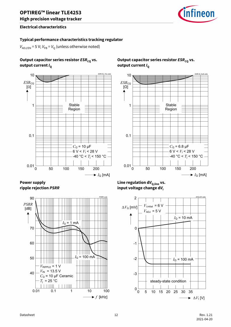
4.1 Tracking regulatorThe output voltage VQ is controlled by comparing it to the voltage applied at pin ADJ/EN and driving a PNPpass transistor accordingly. The control loop stability depends on the output capacitor CQ, the load current,the chip temperature and the poles/zeros introduced by the integrated circuit. To ensure stable operation, theoutput capacitor’s capacitance and its equivalent series resistor ESR requirements given in the table“Functional Range” have to be maintained. For details see also the typical performance graph “OutputCapacitor Series Resistor ESRCQ vs. Output Current IQ”. Also, the output capacitor shall be sized to buffer loadtransients.An input capacitor CI is strongly recommended to buffer line influences. Connect the capacitors close to the ICterminals.Protection circuitry prevent the IC as well as the application from destruction in case of catastrophic events.These safeguards contain output current limitation, reverse polarity protection as well as thermal shutdownin case of overtemperature. In order to avoid excessive power dissipation that could never be handled by the pass element and thepackage, the maximum output current is decreased at high input voltages.An overtemperature protection circuit prevents the IC from immediate destruction under fault conditions(e. g. output continuously short-circuited to GND) by reducing the output current. A thermal balance below200°C junction temperature is established. Please note that a junction temperature above 150°C is outside themaximum ratings and reduces the IC lifetime.The TLE4253 allows a negative supply voltage. However, several small currents are flowing into the IC. Fordetails see electrical characteristics table and typical performance graph. The thermal protection circuit is notoperating during reverse polarity condition.
Datasheet 10 Rev. 1.21 2021-04-20
OPTIREG™ linear TLE4253High precision voltage tracker
Electrical characteristics
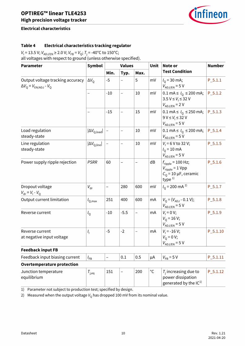
Table 4 Electrical characteristics tracking regulatorVI = 13.5 V; VADJ/EN ≥ 2.0 V; VFB = VQ; Tj = -40°C to 150°C;all voltages with respect to ground (unless otherwise specified).
Parameter Symbol Values Unit Note or Test Condition
NumberMin. Typ. Max.
Output voltage tracking accuracy∆VQ = VEN/ADJ - VQ
∆VQ -5 – 5 mV IQ = 30 mA; VADJ/EN = 5 V
P_5.1.1
– -10 – 10 mV 0.1 mA ≤ IQ ≤ 200 mA; 3.5 V ≤ VI ≤ 32 VVADJ/EN = 2 V
P_5.1.2
– -15 – 15 mV 0.1 mA ≤ IQ ≤ 250 mA; 9 V ≤ VI ≤ 32 VVADJ/EN = 5 V
P_5.1.3
Load regulation steady-state
|∆VQ,load| – – 10 mV 0.1 mA ≤ IQ ≤ 200 mA; VADJ/EN = 5 V
P_5.1.4
Line regulationsteady-state
|∆VQ,line| – – 10 mV VI = 6 V to 32 V; IQ = 10 mAVADJ/EN = 5 V
P_5.1.5
Power supply ripple rejection PSRR 60 – – dB fripple = 100 Hz; Vripple = 1 VppCQ = 10 µF, ceramic type 1)
1) Parameter not subject to production test; specified by design.
P_5.1.6
Dropout voltageVdr = VI - VQ
Vdr – 280 600 mV IQ = 200 mA 2)
2) Measured when the output voltage VQ has dropped 100 mV from its nominal value.
P_5.1.7
Output current limitation IQ,max 251 400 600 mA VQ = (VADJ - 0.1 V);VADJ/EN = 5 V
P_5.1.8
Reverse current IQ -10 -5.5 – mA VI = 0 V; VQ = 16 V;VADJ/EN = 5 V
P_5.1.9
Reverse current at negative input voltage
II -5 -2 – mA VI = -16 V; VQ = 0 V;VADJ/EN = 5 V
P_5.1.10
Feedback input FBFeedback input biasing current IFB – 0.1 0.5 µA VFB = 5 V P_5.1.11
Overtemperature protectionJunction temperature equilibrium
Tj,eq 151 – 200 °C Tj increasing due to power dissipation generated by the IC1)
P_5.1.12
Datasheet 11 Rev. 1.21 2021-04-20
OPTIREG™ linear TLE4253High precision voltage tracker
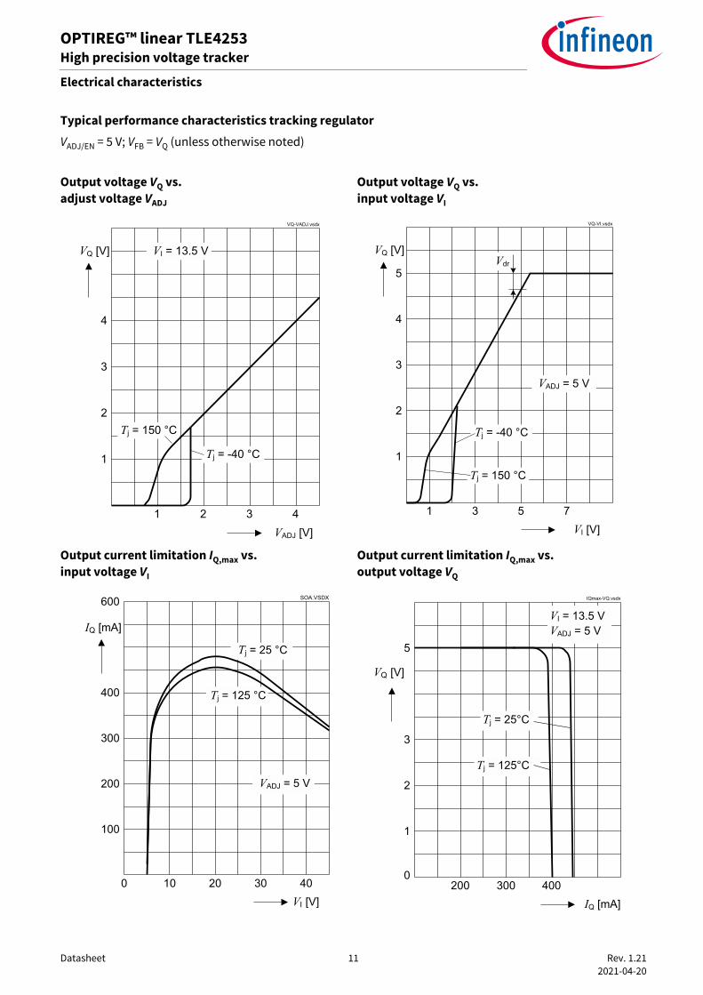
Electrical characteristics
Typical performance characteristics tracking regulatorVADJ/EN = 5 V; VFB = VQ (unless otherwise noted)
Output voltage VQ vs. adjust voltage VADJ
Output voltage VQ vs. input voltage VI
Output current limitation IQ,max vs. input voltage VI
Output current limitation IQ,max vs.output voltage VQ
VQ [V]
VQ-VADJ.vsdx
3
2
1
4
VI = 13.5 V
2 3 41VADJ [V]
Tj = 150 °C
Tj = -40 °C
VQ [V]
VQ-VI.vsdx
3
2
1
4
VADJ = 5 V
5 73VI [V]
Tj = 150 °C
Tj = -40 °C
1
Vdr5
0VI [V]
20 30
IQ [mA]
SOA.VSDX
300
200
100
400
10 40
600
Tj = 25 °C
VADJ = 5 V
Tj = 125 °C
VQ [V]
300 400IQ [mA]
IQmax-VQ.vsdx
3
2
1
2000
5
VI = 13.5 VVADJ = 5 V
Tj = 125°C
Tj = 25°C
Datasheet 12 Rev. 1.21 2021-04-20
OPTIREG™ linear TLE4253High precision voltage tracker
Electrical characteristics
Typical performance characteristics tracking regulatorVADJ/EN = 5 V; VFB = VQ (unless otherwise noted)
Output capacitor series resistor ESRCQ vs.output current IQ
Output capacitor series resistor ESRCQ vs.output current IQ
Power supply ripple rejection PSRR
Line regulation dVQ,line vs. input voltage change dVI
ESR-IQ_10u.vsdx
1
0.1
0.01
ESRCQ[Ω]
0IQ [mA]
100 15050 200
10
CQ = 10 μF6 V < VI < 28 V-40 °C < Tj < 150 °C
Stable Region
ESR-IQ_6u8.vsdx
1
0.1
0.01
ESRCQ[Ω]
0IQ [mA]
100 15050 200
10
CQ = 6.8 μF6 V < VI < 28 V-40 °C < Tj < 150 °C
Stable Region
0.01f [kHz]
10
PSRR[dB]
PSRR.vsdx
70
60
0.1 1 100
90
40
50
IQ = 1 mA
VRIPPLE = 1 VVIN = 13.5 VCQ = 10 μF CeramicTj = 25 °C
IQ = 100 mA
0∆VI [V]
5 15 20 30 35
∆VQ [mV]
dVQ-dVI.vsdx
-1
-2
-3
0
10 25
2
0
IQ = 10 mA
steady-state condition
VI,initial = 6 VVADJ = 5 V
IQ = 100 mA
Datasheet 13 Rev. 1.21 2021-04-20
OPTIREG™ linear TLE4253High precision voltage tracker
Electrical characteristics
Typical performance characteristics tracking regulatorVADJ/EN = 5 V; VFB = VQ (unless otherwise noted)
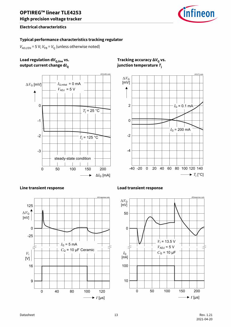
Load regulation dVQ,line vs. output current change dIQ
Tracking accuracy ∆VQ vs. junction temperature Tj
Line transient response Load transient response
0∆IQ [mA]
100 150 200
∆VQ [mV]
dVQ-dIQ.vsdx
-1
-2
-3
0
50
Tj = 125 °C
Tj = 25 °C
steady-state condition
IQ,initial = 0 mAVADJ = 5 V
-40Tj [°C]
-20 20 40 80 100
∆VQ [mV]
dVQ-Tj.vsdx
0
-2
-4
2
0 60 140120
IQ = 0.1 mA
IQ = 200 mA
0t [μs]
80 100
∆VQ [mV]
dVI-reponse.vsdx
16
9
40 120
VI [V]
IQ = 5 mACQ = 10 μF Ceramic
-25
125
0
0t [μs]
100 150
∆VQ [mV]
dIQresponse.vsdx
100
10
0
50 200
IQ [mA]
VI = 13.5 VVADJ = 5 VCQ = 10 μF
50
Datasheet 14 Rev. 1.21 2021-04-20
OPTIREG™ linear TLE4253High precision voltage tracker
Electrical characteristics
Typical performance characteristics tracking regulatorVADJ/EN = 5 V; VFB = VQ (unless otherwise noted)
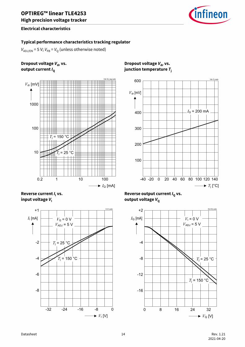
Dropout voltage Vdr vs.output current IQ
Dropout voltage Vdr vs. junction temperature Tj
Reverse current II vs. input voltage VI
Reverse output current IQ vs. output voltage VQ
0.2IQ [mA]
1 10
Vdr-IQ_log.vsdx
100
10
1000
100
Vdr [mV]
Tj = 150 °C
Tj = 25 °C
-40Tj [°C]
-20 20 40 80 100
Vdr [mV]
Vdr-Tj.vsdx
300
200
100
400
0 60 140120
600
IQ = 200 mA
-32VI [V]
-16 -8
II [mA]
II-VI.vsdx
-4
-6
-8
-2
-24 0
+1
Tj = 150 °C
Tj = 25 °C
VQ = 0 VVADJ = 5 V
0VQ [V]
16 24
IQ [mA]
IQ-VQ.vsdx
-8
-12
-16
-4
8 32
+2
VI = 0 VVADJ = 5 V
Tj = 150 °C
Tj = 25 °C
Datasheet 15 Rev. 1.21 2021-04-20
OPTIREG™ linear TLE4253High precision voltage tracker
Electrical characteristics
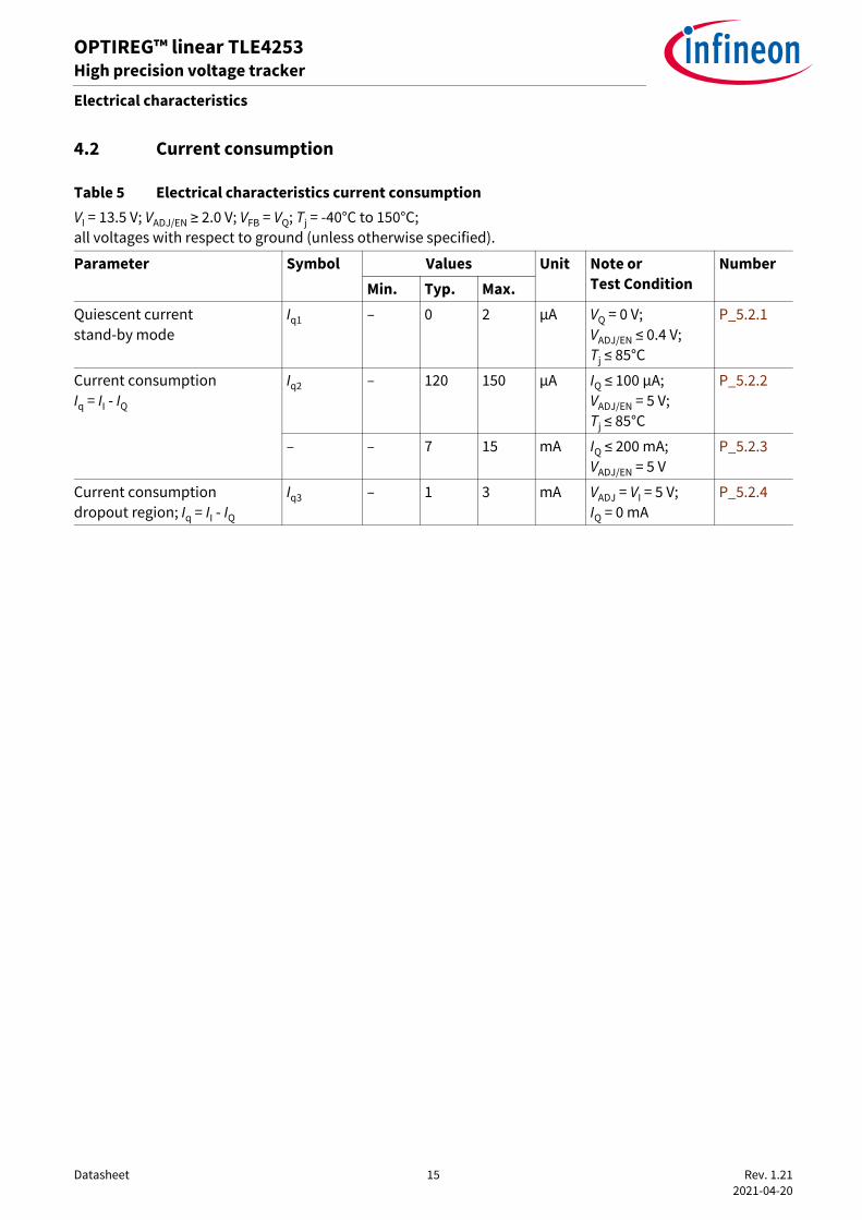
4.2 Current consumption
Table 5 Electrical characteristics current consumptionVI = 13.5 V; VADJ/EN ≥ 2.0 V; VFB = VQ; Tj = -40°C to 150°C;all voltages with respect to ground (unless otherwise specified).
Parameter Symbol Values Unit Note or Test Condition
NumberMin. Typ. Max.
Quiescent current stand-by mode
Iq1 – 0 2 µA VQ = 0 V; VADJ/EN ≤ 0.4 V; Tj ≤ 85°C
P_5.2.1
Current consumption Iq = II - IQ
Iq2 – 120 150 µA IQ ≤ 100 µA; VADJ/EN = 5 V;Tj ≤ 85°C
P_5.2.2
– – 7 15 mA IQ ≤ 200 mA; VADJ/EN = 5 V
P_5.2.3
Current consumption dropout region; Iq = II - IQ
Iq3 – 1 3 mA VADJ = VI = 5 V; IQ = 0 mA
P_5.2.4
Datasheet 16 Rev. 1.21 2021-04-20
OPTIREG™ linear TLE4253High precision voltage tracker
Electrical characteristics
Typical performance characteristics tracking regulatorVADJ/EN = 5 V; VFB = VQ (unless otherwise noted)
Current consumption Iq2 vs. junction temperature Tj
Current consumption Iq vs. output current IQ
Current consumption Iq vs. input voltageVI
Quiescent current Iq1 vs. junction temperature Tj
Iq2-Tj.vsdx
1
0.1
0.01
10
Iq [mA]
-40Tj [°C]
-20 20 40 80 1000 60 140120
VI = 13.5V
IQ = 200 μA
IQ = 200 mA
0.2IQ [mA]
1 10
Iq-IQ.vsdx
1
0.1
0.01
10
100
Iq [mA]
VI = 6 V
VI > 9 V
VEN/ADJ = 5 V
Iq-VI.vsdx
0
5
10
15
20
25
30
0 10 20 30 40
V I [V]
I q[m
A]
RLOAD = 25 ΩRLOAD = 50 ΩRLOAD = 100 ΩRLOAD = 500 Ω
Iq1-Tj.vsdx
1
0.1
Iq1 [μA]
-40Tj [°C]
-20 20 40 80 1000 60 140120
VI = 13.5VVEN/ADJ = 0 V
Datasheet 17 Rev. 1.21 2021-04-20
OPTIREG™ linear TLE4253High precision voltage tracker
Electrical characteristics
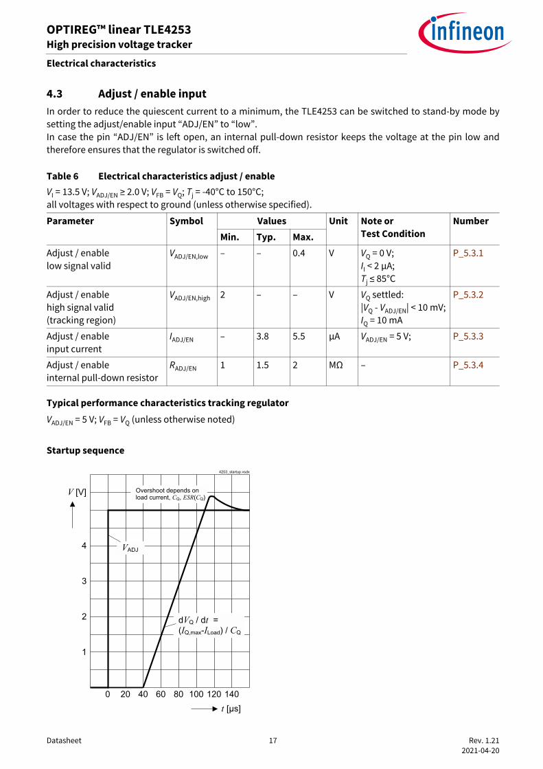
4.3 Adjust / enable input In order to reduce the quiescent current to a minimum, the TLE4253 can be switched to stand-by mode bysetting the adjust/enable input “ADJ/EN” to “low”.In case the pin “ADJ/EN” is left open, an internal pull-down resistor keeps the voltage at the pin low andtherefore ensures that the regulator is switched off.
Typical performance characteristics tracking regulatorVADJ/EN = 5 V; VFB = VQ (unless otherwise noted)
Table 6 Electrical characteristics adjust / enable VI = 13.5 V; VADJ/EN ≥ 2.0 V; VFB = VQ; Tj = -40°C to 150°C; all voltages with respect to ground (unless otherwise specified).
Parameter Symbol Values Unit Note or Test Condition
NumberMin. Typ. Max.
Adjust / enable low signal valid
VADJ/EN,low – – 0.4 V VQ = 0 V; II < 2 µA;Tj ≤ 85°C
P_5.3.1
Adjust / enable high signal valid(tracking region)
VADJ/EN,high 2 – – V VQ settled: |VQ - VADJ/EN| < 10 mV; IQ = 10 mA
P_5.3.2
Adjust / enable input current
IADJ/EN – 3.8 5.5 µA VADJ/EN = 5 V; P_5.3.3
Adjust / enable internal pull-down resistor
RADJ/EN 1 1.5 2 MΩ – P_5.3.4
Startup sequence
0t [μs]
20 60 80 120 140
V [V]
4253_startup.vsdx
3
2
1
4
40 100
VADJ
dVQ / dt = (IQ,max-ILoad) / CQ
Overshoot depends on load current, CQ, ESR(CQ)
Datasheet 18 Rev. 1.21 2021-04-20
OPTIREG™ linear TLE4253High precision voltage tracker
Application information
5 Application information
Note: The following information is given as a hint for the implementation of the device only and shall not be regarded as a description or warranty of a certain functionality, condition or quality of the device.The application circuits shown are simplified examples. The function must be verified in the real application.
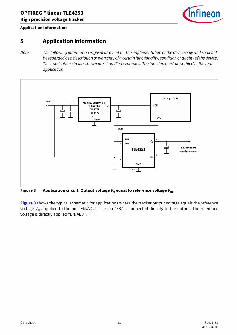
Figure 3 Application circuit: Output voltage VQ equal to reference voltage VREF
Figure 3 shows the typical schematic for applications where the tracker output voltage equals the referencevoltage VREF applied to the pin “EN/ADJ”. The pin “FB” is connected directly to the output. The referencevoltage is directly applied “EN/ADJ”.
ADJ
I FB
QEN/
GND
TLE4253
8
2, 3, 6, 7
5
4
1
μC, e.g. C167
VDD
I/O
Main μC supply, e.g. TLE4271-2TLE4278TLE4470
etc.
I Q
GND
VBAT
e.g. off board supply, sensors
VREF
Datasheet 19 Rev. 1.21 2021-04-20
OPTIREG™ linear TLE4253High precision voltage tracker
Application information
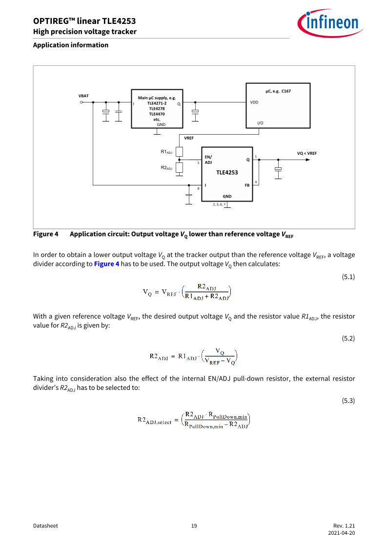
Figure 4 Application circuit: Output voltage VQ lower than reference voltage VREF
In order to obtain a lower output voltage VQ at the tracker output than the reference voltage VREF, a voltagedivider according to Figure 4 has to be used. The output voltage VQ then calculates:
(5.1)
With a given reference voltage VREF, the desired output voltage VQ and the resistor value R1ADJ, the resistorvalue for R2ADJ is given by:
(5.2)
Taking into consideration also the effect of the internal EN/ADJ pull-down resistor, the external resistordivider’s R2ADJ has to be selected to:
(5.3)
EN/ADJ
I
Q
GND
TLE4253
8
5
1
μC, e.g. C167
VDD
I/O
Main μC supply, e.g. TLE4271-2TLE4278TLE4470
etc.
I Q
GND
VBAT
VQ < VREFR1ADJ
R2ADJ
VREF
FB4
2, 3, 6, 7
Datasheet 20 Rev. 1.21 2021-04-20
OPTIREG™ linear TLE4253High precision voltage tracker
Application information
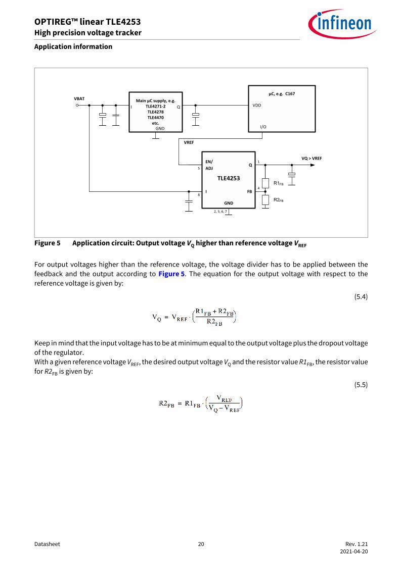
Figure 5 Application circuit: Output voltage VQ higher than reference voltage VREF
For output voltages higher than the reference voltage, the voltage divider has to be applied between thefeedback and the output according to Figure 5. The equation for the output voltage with respect to thereference voltage is given by:
(5.4)
Keep in mind that the input voltage has to be at minimum equal to the output voltage plus the dropout voltageof the regulator. With a given reference voltage VREF, the desired output voltage VQ and the resistor value R1FB, the resistor valuefor R2FB is given by:
(5.5)
4
ADJ
I FB
QEN/
GND
TLE4253
8
2, 3, 6, 7
5
1
μC, e.g. C167
VDD
I/O
Main μC supply, e.g. TLE4271-2TLE4278TLE4470
etc.
I Q
GND
VBAT
VQ > VREF
VREF
R1FB
R2FB
Datasheet 21 Rev. 1.21 2021-04-20
OPTIREG™ linear TLE4253High precision voltage tracker
Package outlines
6 Package outlines
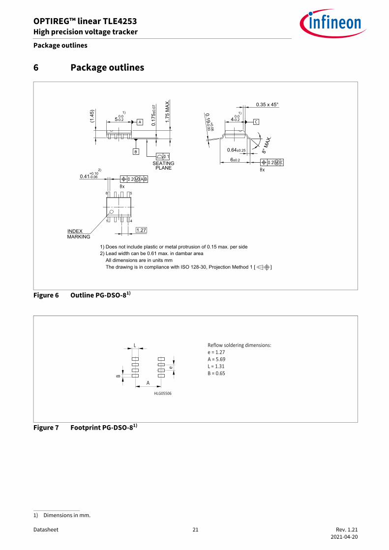
Figure 6 Outline PG-DSO-81)
Figure 7 Footprint PG-DSO-81)
1) Dimensions in mm.
2) Lead width can be 0.61 max. in dambar area1) Does not include plastic or metal protrusion of 0.15 max. per side
INDEXMARKING
1.27
5 0.0-0.2
0.41+0.10-0.06
2)
1)
0.17
5±0.
07
1.75
MAX
.SEATING
PLANE
(1.4
5)
4 0.0-0.2
0.35 x 45°1)0.19 +0.06
-0.00
6±0.2
0.64±0.25
1 4
8 5
8° M
AX.
The drawing is in compliance with ISO 128-30, Projection Method 1 [ ]All dimensions are in units mm
HLG05506
e
A
B
L Reflow soldering dimensions:e = 1.27A = 5.69L = 1.31B = 0.65
Datasheet 22 Rev. 1.21 2021-04-20
OPTIREG™ linear TLE4253High precision voltage tracker
Package outlines
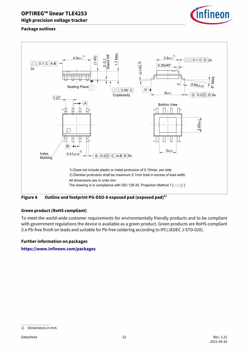
Figure 8 Outline and footprint PG-DSO-8 exposed pad (exposed pad)1)
Green product (RoHS compliant)To meet the world-wide customer requirements for environmentally friendly products and to be compliantwith government regulations the device is available as a green product. Green products are RoHS-compliant(i.e Pb-free finish on leads and suitable for Pb-free soldering according to IPC/JEDEC J-STD-020).
Further information on packageshttps://www.infineon.com/packages
1) Dimensions in mm.
2.65
±0.2
3±0.2
Bottom View
1
58
4
IndexMarking
B
A
0.1 C A-B
0.2 C A-B D 8x2)
Stan
d O
ff
Seating Plane0.08 C
Coplanarity
2x
(1.4
5)
0..0
.1
1.7
Max
.
0.41±0.09
1.27
4.9±0.1
6±0.2D
0.2 D 8x
1) 3.9±0.11)
0.1 C D 2x0.19+0.06
0.64±0.25
0.35x45°
14
5 8
8° M
AX.
The drawing is in compliance with ISO 128-30, Projection Method 1 [ ]
2) Dambar protrusion shall be maximum 0.1mm total in excess of lead width1) Does not include plastic or metal protrusion of 0.15max. per side
All dimensions are in units mm
Datasheet 23 Rev. 1.21 2021-04-20
OPTIREG™ linear TLE4253High precision voltage tracker
Revision history
7 Revision history
Revision Date Changes1.21 2021-04-20 Editorial changes.
Correct “Non inverting” to “Inverting” in the description of the FB pin in “Pin definitions and functions” on Page 5.Assigned the parameter “Adjust / enable input voltage (voltage tracking range)” on Page 7 the number P_4.2.5.Split the previous figure 6 into Figure 6 “Outline PG-DSO-8” on Page 21 and Figure 7 “Footprint PG-DSO-81)” on Page 21. (The old figure 7 is now Figure 8 “Outline and footprint PG-DSO-8 exposed pad (exposed pad)” on Page 22.)
1.2 2009-11-09 Updated Version Data Sheet, version TLE4253E in PG-DSO-8 exposed pad and all related description added:In “Features” on Page 1 picture for package PG-DSO-8 updatedIn “Features” on Page 1 “package” replaced by “packages”In “Description” on Page 1 “a small PG-DSO-8 package” replaced by “small PG-DSO-8 packages”; “The exposed pad (EP) package variant PG-DSO-8 exposed pad offers extremely low thermal resistance.” added; “suits” replaces by “makes”In “Pin assignment” on Page 5, package PG-DSO-8 exposed pad addedIn “Pin definitions and functions” on Page 5 all definition for package PG-DSO-8 exposed pad addedIn “Thermal resistance” on Page 8 all values for package PG-DSO-8 exposed pad added (P_4.3.6 - P_4.3.10)In “Adjust / enable input” on Page 17 typo corrected: “resistors” replaced by “resistor”In “Package outlines” on Page 21 package PG-DSO-8 exposed pad added
1.1 2008-08-19 Updated Version Final Datasheet for TLE4253GS:“Package outlines” on Page 21 updated;In “Typical performance characteristics tracking regulator” on Page 16 Graph “Current consumption Iq vs. input voltageVI” on Page 16 added
1.0 2007-07-10 Initial Final Datasheet for TLE4253GS.For the TLE4253ES (exposed pad) product variant, please refer to the respective datasheet

TrademarksAll referenced product or service names and trademarks are the property of their respective owners.
Edition 2021-04-20Published by Infineon Technologies AG81726 Munich, Germany
© 2021 Infineon Technologies AG.All Rights Reserved.
Do you have a question about any aspect of this document?Email: [email protected]
Document referenceZ8F55248541
IMPORTANT NOTICEThe information given in this document shall in noevent be regarded as a guarantee of conditions orcharacteristics ("Beschaffenheitsgarantie"). With respect to any examples, hints or any typicalvalues stated herein and/or any information regardingthe application of the product, Infineon Technologieshereby disclaims any and all warranties and liabilitiesof any kind, including without limitation warranties ofnon-infringement of intellectual property rights of anythird party. In addition, any information given in this document issubject to customer's compliance with its obligationsstated in this document and any applicable legalrequirements, norms and standards concerningcustomer's products and any use of the product ofInfineon Technologies in customer's applications. The data contained in this document is exclusivelyintended for technically trained staff. It is theresponsibility of customer's technical departments toevaluate the suitability of the product for the intendedapplication and the completeness of the productinformation given in this document with respect tosuch application.
For further information on technology, delivery termsand conditions and prices, please contact the nearestInfineon Technologies Office (www.infineon.com).
WARNINGSDue to technical requirements products may containdangerous substances. For information on the typesin question please contact your nearest InfineonTechnologies office.
Except as otherwise explicitly approved by InfineonTechnologies in a written document signed byauthorized representatives of Infineon Technologies,Infineon Technologies’ products may not be used inany applications where a failure of the product or anyconsequences of the use thereof can reasonably beexpected to result in personal injury.