Embed Size (px)
Citation preview

ARL-TR-7462 ● SEP 2015
US Army Research Laboratory
Optimization of a Circularly Polarized Patch Antenna for Two Frequency Bands
by Jahin S Habib Approved for public release; distribution is unlimited.

NOTICES
Disclaimers
The findings in this report are not to be construed as an official Department of the
Army position unless so designated by other authorized documents.
Citation of manufacturer’s or trade names does not constitute an official
endorsement or approval of the use thereof.
Destroy this report when it is no longer needed. Do not return it to the originator.
ARL-TR-7462 ● SEP 2015
US Army Research Laboratory
Optimization of a Circularly Polarized Patch Antenna for Two Frequency Bands
by Jahin S Habib Sensors and Electron Devices Directorate, ARL
Approved for public release; distribution is unlimited.
ii
REPORT DOCUMENTATION PAGE Form Approved
OMB No. 0704-0188 Public reporting burden for this collection of information is estimated to average 1 hour per response, including the time for reviewing instructions, searching existing data sources, gathering and maintaining the
data needed, and completing and reviewing the collection information Send comments regarding this burden estimate or any other aspect of this collection of information, including suggestions for reducing the
burden, to Department of Defense, Washington Headquarters Services, Directorate for Information Operations and Reports (0704-0188), 1215 Jefferson Davis Highway, Suite 1204, Arlington, VA 22202-4302
Respondents should be aware that notwithstanding any other provision of law, no person shall be subject to any penalty for failing to comply with a collection of information if it does not display a currently
valid OMB control number
PLEASE DO NOT RETURN YOUR FORM TO THE ABOVE ADDRESS.
1. REPORT DATE (DD-MM-YYYY)
Sep 2015
2. REPORT TYPE
Final
3. DATES COVERED (From - To)
4. TITLE AND SUBTITLE
Optimization of a Circularly Polarized Patch Antenna for Two Frequency Bands
5a. CONTRACT NUMBER
5b. GRANT NUMBER
5c. PROGRAM ELEMENT NUMBER
6. AUTHOR(S)
Jahin S Habib
5d. PROJECT NUMBER
5e. TASK NUMBER
5f. WORK UNIT NUMBER
7. PERFORMING ORGANIZATION NAME(S) AND ADDRESS(ES)
US Army Research Laboratory
ATTN: RDRL-SER-M
2800 Powder Mill Road
Adelphi, MD 20783-1138
8. PERFORMING ORGANIZATION REPORT NUMBER
ARL-TR-7462
9. SPONSORING/MONITORING AGENCY NAME(S) AND ADDRESS(ES)
10. SPONSOR/MONITOR'S ACRONYM(S)
11. SPONSOR/MONITOR'S REPORT NUMBER(S)
12. DISTRIBUTION/AVAILABILITY STATEMENT
Approved for public release; distribution is unlimited.
13. SUPPLEMENTARY NOTES
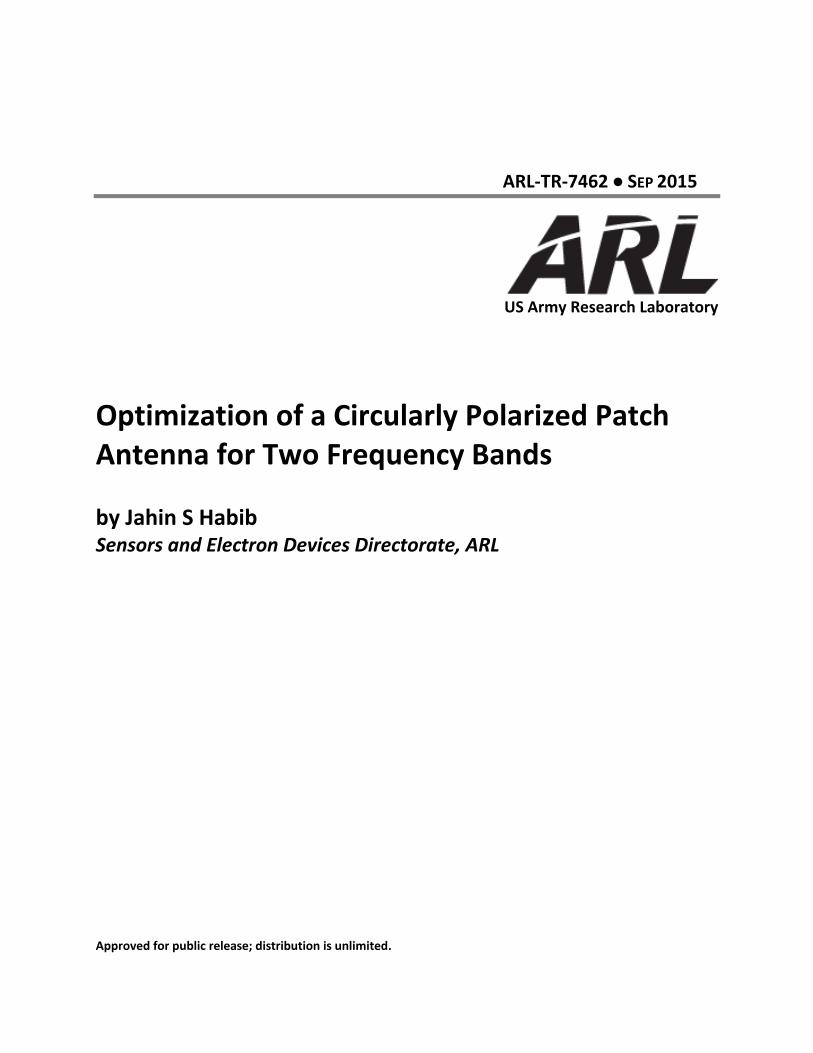
14. ABSTRACT
The objective of this project is to gain a better understanding of the various techniques that can be used to improve the
performance of a circularly polarized microstrip patch antenna. These adjustments include tuning the feed point along
different positions on the surface of the patch, analyzing assorted dielectric materials with differing dielectric constants, and
optimizing the axial ratio based on the geometry of a circularly polarized patch. Testing the feed point in various locations on
the patch allows the designer to improve the S11 and radiation pattern—a peak broadside polar radiation plot is anticipated for
optimum performance. Using a high permittivity dielectric lowers the resonant frequency of the patch, allowing the designer
to shrink the size of the patch. Altering the patch geometry and optimizing the axial ratio by using a “notching” technique
allows the designer to choose from multiple polarization types. With empirical simulations via the High Frequency Structural
Simulator (HFSS), expanding this idea for future research will result in producing a scalable multiband microstrip antenna.
15. SUBJECT TERMS
Patch Antenna, Circular Polarization
16. SECURITY CLASSIFICATION OF: 17. LIMITATION OF ABSTRACT
UU
18. NUMBER OF PAGES
36
19a. NAME OF RESPONSIBLE PERSON
Gregory A Mitchell a. REPORT
Unclassified
b. ABSTRACT
Unclassified
c. THIS PAGE
Unclassified
19b. TELEPHONE NUMBER (Include area code)
301-394-2322 Standard Form 298 (Rev. 8/98)
Prescribed by ANSI Std. Z39.18

iii
Contents
List of Figures iv
List of Tables v
Acknowledgments vii
Student Bio ix
1. Introduction/Background 1
1.1 Frequency Ranges 1
1.2 Basic Patch Antenna Design 1
1.3 Dielectric Materials 2
1.4 Circular Polarization 2
2. Experiment and Calculations 5
2.1 Patch on Rogers 5870 8
2.2 Patch Rogers 6010 14
3. Results and Discussion 20
4. Future Work 20
5. References 23
Distribution List 26

iv
List of Figures
Fig. 1 Linear polarization vs. CP ......................................................................3
Fig. 2 SF = 0 .....................................................................................................3
Fig. 3 SF = 0.25 ................................................................................................4
Fig. 4 SF = 0.75 ................................................................................................4
Fig. 5 SF = 1.25 ................................................................................................5
Fig. 6 Transverse plane (XY plane) of patch ...................................................6
Fig. 7 Normal (YZ) plane of patch antenna .....................................................7
Fig. 8 HFSS patch antenna model, 3-dimensional view ..................................7
Fig. 9 Return loss for varying feed points in Rogers 5870. Best S11 curve corresponds to Cy = 2 mm. ....................................................................9
Fig. 10 Probe 2 mm away from center position, which corresponds to a 9.26-GHz frequency .....................................................................................10
Fig. 11 Return loss for varying SF in Rogers 5870 ..........................................11
Fig. 12 SF = 0.46 on Rogers 5870 substrate with feed point 2 mm from center position .................................................................................................12
Fig. 13 Axial ratio for the best SF—corresponds to 9.35 GHz with an optimal axial ratio of 1.11 dB ...........................................................................13
Fig. 14 Radiation plot at 9.35 GHz for optimal axial ratio. Boresight pattern with a 6.19-dB gain. ............................................................................14
Fig. 15 Return loss for varying feed points in Rogers 6010. Best S11 curve corresponds to Cy=2.4 mm. .................................................................15
Fig. 16 Probe 2.4 mm away from center position, which corresponds to a 2.83-GHz frequency .....................................................................................16
Fig. 17 Return loss for varying SF in Rogers 6010 ..........................................17
Fig. 18 SF = 0.21 on Rogers 6010 substrate with feed point 2.4 mm from center position ......................................................................................18
Fig. 19 Rogers 6010 axial ratio for the best SF—corresponds to 2.83 GHz with an optimal axial ratio of 1.61 dB .........................................................19
Fig. 20 Rogers 6010 radiation plot at 2.83 GHz for optimal axial ratio. Boresight pattern with a 4.62-dB gain. ................................................20
Fig. 21 Transverse (XY) plane of the proposed dual-band antenna design .....21
Fig. 22 HFSS model of the dual-band antenna, 3-dimensional view ...............22

v
List of Tables
Table 1 Variable list for Rogers 5870 .................................................................8
Table 2 Variable list for Rogers 6010 .................................................................8

vi
INTENTIONALLY LEFT BLANK.

vii
Acknowledgments
I would like to thank my mentor, Gregory Mitchell, for his continuous support,
motivation, and knowledge for my project this summer. I would also like to thank
Theodore Anthony and Dr Amir Zaghloul for their countless hours of teaching
and advice.

viii
INTENTIONALLY LEFT BLANK.

ix
Student Bio
Jahin Habib is a rising senior at Virginia Polytechnic Institute and State
University (Virginia Tech), majoring in electrical engineering. She was able to
research autonomous vehicles at Virginia Tech during the summer of 2013.
Recently, she gained valuable hands-on experience at United Technologies
Corporation as an electronics engineering intern during the summer of 2014.
Working there greatly influenced her toward a path in electromagnetic fields.
Throughout her time at Virginia Tech, Habib has remained involved in a variety
of organizations. She is currently a student ambassador for the Bradley
Department of Electrical and Computer Engineering and will be serving as
president for Virginia Tech’s IEEE Student Branch this upcoming school year.

10
INTENTIONALLY LEFT BLANK.
1
1. Introduction/Background
Patch antennas gained popularity in the 1970s as advancements in size and
performance became useful in communication systems. Compared to its
predecessors, such as traditional parabolic reflectors and large-scale antennas, the
flat shape and reduced weight of the patch antenna allowed for great flexibility in
various space and airborne applications. The use of dielectric materials to further
reduce the size of the antenna has allowed technological advancements in global
positioning system (GPS) and other wireless devices.1 Recently, studies on dual-
band antennas have emerged to eliminate the restriction on using just 1 frequency
band. Empirical work via the High Frequency Structural Simulator (HFSS) has
allowed engineers to create scalable multiband microstrip antennas. Several
factors were taken into consideration when creating a dual-band antenna to ensure
optimal performance in this study. These factors include optimizing the patch
length, adjusting the feed point along the patch, varying the height of the
dielectric substrates, and using a “notching” technique to incorporate circular
polarization (CP).
1.1 Frequency Ranges
When comparing X- and S-band ranges, many differences can be noted as the 2
operate at special frequencies and have variations in their respective parameters.
While the X-band operates at 8–12 GHz, the S-band operates at 2–4 GHz in radar
engineering. Due to the shorter wavelengths, which, in turn, allow for high
resolution imagery, the antennas operating at X-band are small and very portable.
On the other hand, antennas operating at the S-band are larger in size. The
motivation behind creating a dual-band antenna came from the idea of eliminating
the restriction of picking just 1 frequency band, and instead, combining the 2 to
form a single element.
1.2 Basic Patch Antenna Design
The patch antenna, also known as the microstrip antenna, is commonly used at
frequencies greater than 1 GHz (microwave frequencies). The most common
configurations of patch antennas are found in square, rectangular, or circular
shapes made out of conductive material. They are approximately /2 in size and
placed a small fraction above the ground plane with dielectric material in
between. The electrical half-wavelength length of the patch also includes the
shortening effect of the material’s dielectric constant (r), as follows

2
L=λ0
2√ϵr (1)
These low volume and lightweight devices are highly advantageous as the flat
structure permits a large aperture with a corresponding high gain value. Their
2-dimensional structure allows for manipulation to fit different applications.3
Once it is tuned to the operating frequency, the patch will achieve maximum
radiation efficiency, which is normal to the plane of the patch. A coaxial probe
will be used in this study to feed the microstrip antenna; the inner conductor of
the coaxial cable is shorted to the patch while the outer conductor is attached to
the ground plane.
1.3 Dielectric Materials
As r increases, the frequency at which the patch resonates at will decrease, and
vice versa. Thinner substrates demonstrate benefits as they minimize excessive
radiation and coupling due to the tightly bound fields.2 In this study of the CP
patch antenna, the X-band element will include a patch and ground plane
separated by Rogers 5870 dielectric with r=2.33. The S-band will include a patch
and ground plane separated by Rogers 6010 dielectric with r=10.2.
1.4 Circular Polarization
Antennas that are linearly polarized can transmit and receive linearly polarized
signals. Consider a telephone pole that sends out and receives messages. In order
for the receiving pole to obtain a vertically polarized signal, the transmitting pole
must send out a signal that is vertically polarized. If the receiving pole is
horizontally polarized and the transmitting pole is vertically polarized, the
message will not convey. CP enables the use of both horizontal and vertical
antennas for receiving, as the polarization continuously rotates during
transmission. The CP wave does not experience any changes other than a change
in direction in a rotational manner. In Fig. 1, we see that the electric-field vector
produces a circle in the XY plane.

3
Fig. 1 Linear polarization vs. CP
The square and circular shaped patch antennas discussed thus far radiate linearly
polarized waves. Modifications can be made on these elements to obtain CP. One
of the methods include trimming the opposite corners of the patch, also known as
the notching technique, to create diagonal resonances, which then leads to
degeneration. As a result, this allows the antenna to radiate a CP wave. In this
study, we used the following formula to solve for the notching value by applying
a scaling factor (SF) to the patch.
Notching Value =L
2(1 − SF) (2)
In Figs. 2 through 5, it can be seen that as SF increases, the size of the notch at
each corner increases as well.
Fig. 2 SF = 0

4
Fig. 3 SF = 0.25
Fig. 4 SF = 0.75

5
Fig. 5 SF = 1.25
2. Experiment and Calculations
For simulation purposes, the 2 patches with varying dielectric materials were
tested separately for initial comparison. Figures 6 through 8 exhibit the variables
used in this study to calculate the various antenna parameters. The coaxial probe,
which acts as a feed point, is designed to have a 50-Ω impedance. The variable
list is shown in Tables 1 and 2 for the S-band patch and the X-band patch,
respectively.

6
Fig. 6 Transverse plane (XY plane) of patch
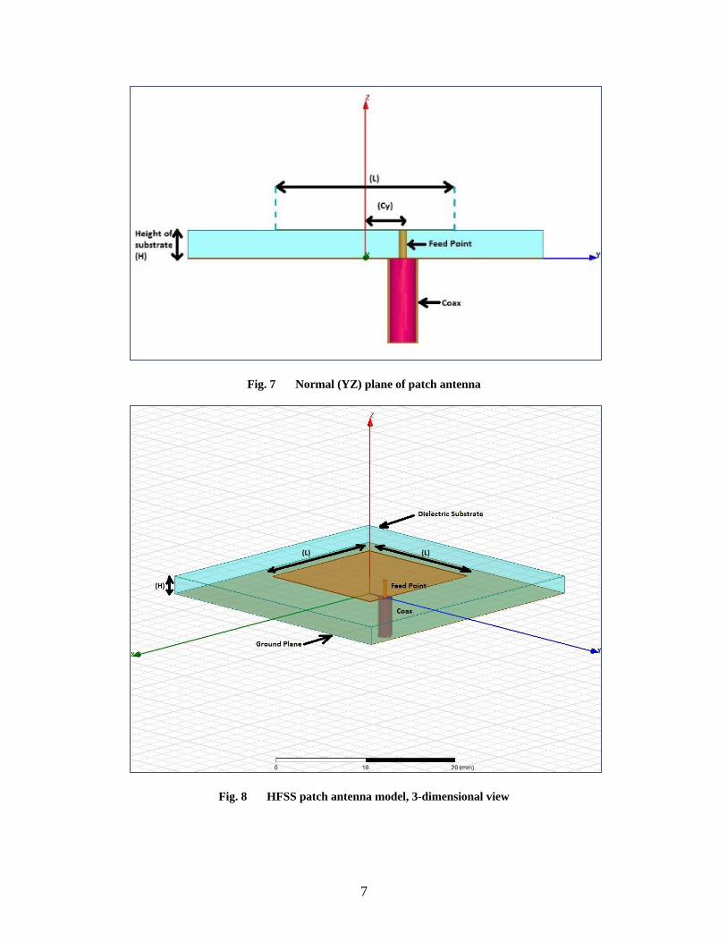
7
Fig. 7 Normal (YZ) plane of patch antenna
Fig. 8 HFSS patch antenna model, 3-dimensional view

8
Table 1 Variable list for Rogers 5870
Name Description Value/Unit
L Length of Patch Antenna 10.5 mm
Cx X-direction of coax 0
Cy Y-direction of coax 0
Cz Z-direction of coax 0
H Height of dielectric 1.5 mm
NV Notching Value 0
Table 2 Variable list for Rogers 6010
Name Description Value/Unit
L Length of Patch Antenna 16.5 mm
Cx X-direction of coax 0
Cy Y-direction of coax 0
Cz Z-direction of coax 0
h Height of dielectric 2 mm
NV Notching Value 0
2.1 Patch on Rogers 5870
We wanted the X-band element to radiate at 9.35 GHz on the Rogers 5870
material. As a result, the patch length was calculated as follows
𝜆 =c (Speed of Light)
f ∗ (√ϵrμr)=
3 ∗ 108
(9.35 ∗ 109) ∗ (√2.33)≈ 0.021 m;
𝑳 =λ
2=0.021
2≈ 𝟏𝟎. 𝟓 𝐦𝐦
Table 1 displays the variables used to design the antenna to verify the HFSS
simulation setup.
The feed point was swept from the center of the patch (0,0,0) to the outer edge
(0,3.2,0) to locate the position at which the patch resonated best. As shown in
Fig. 9, the S11 plot shows that the best curve corresponds to a 9.26-GHz
frequency with a –25.71-dB null. This occurs when the probe is 2 mm away from
the center position of the patch, as shown in Fig. 10.

9
Fig. 9 Return loss for varying feed points in Rogers 5870. Best S11 curve corresponds to
Cy = 2 mm.

10
Fig. 10 Probe 2 mm away from center position, which corresponds to a 9.26-GHz
frequency
Next, the notching technique was implemented by trimming opposite corners of
the patch. A parameter sweep was performed on HFSS from a 0.36 to 0.51 SF. As
shown in Fig. 11, the best S11 curve is found when the scaling factor was equal to
0.46 resulting in a notching value of 2.83 mm shown in Fig. 12.
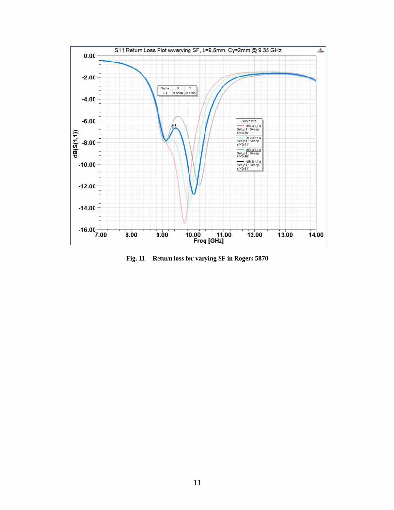
11
Fig. 11 Return loss for varying SF in Rogers 5870

12
Fig. 12 SF = 0.46 on Rogers 5870 substrate with feed point 2 mm from center position
After finding the best SF to notch the patch, an axial ratio calculation was
performed, as shown in Fig. 13. With the coax probe 2 mm away from the center
of the patch, the best SF value of 0.46 corresponds to 9.35 GHz with an optimal
axial ratio at 1.11 dB.
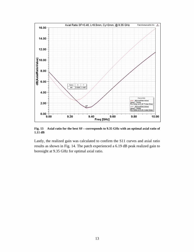
13
Fig. 13 Axial ratio for the best SF—corresponds to 9.35 GHz with an optimal axial ratio of
1.11 dB
Lastly, the realized gain was calculated to confirm the S11 curves and axial ratio
results as shown in Fig. 14. The patch experienced a 6.19 dB peak realized gain to
boresight at 9.35 GHz for optimal axial ratio.
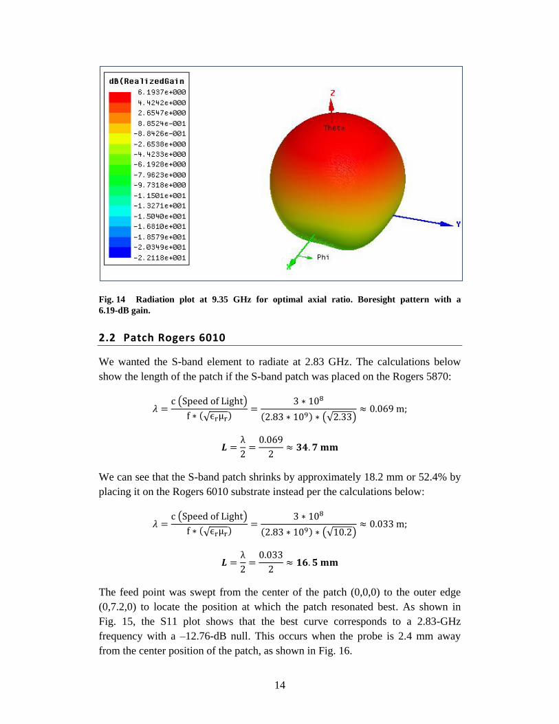
14
Fig. 14 Radiation plot at 9.35 GHz for optimal axial ratio. Boresight pattern with a
6.19-dB gain.
2.2 Patch Rogers 6010
We wanted the S-band element to radiate at 2.83 GHz. The calculations below
show the length of the patch if the S-band patch was placed on the Rogers 5870:
𝜆 =c (Speed of Light)
f ∗ (√ϵrμr)=
3 ∗ 108
(2.83 ∗ 109) ∗ (√2.33)≈ 0.069 m;
𝑳 =λ
2=0.069
2≈ 𝟑𝟒. 𝟕 𝐦𝐦
We can see that the S-band patch shrinks by approximately 18.2 mm or 52.4% by
placing it on the Rogers 6010 substrate instead per the calculations below:
𝜆 =c (Speed of Light)
f ∗ (√ϵrμr)=
3 ∗ 108
(2.83 ∗ 109) ∗ (√10.2)≈ 0.033 m;
𝑳 =λ
2=0.033
2≈ 𝟏𝟔. 𝟓 𝐦𝐦
The feed point was swept from the center of the patch (0,0,0) to the outer edge
(0,7.2,0) to locate the position at which the patch resonated best. As shown in
Fig. 15, the S11 plot shows that the best curve corresponds to a 2.83-GHz
frequency with a –12.76-dB null. This occurs when the probe is 2.4 mm away
from the center position of the patch, as shown in Fig. 16.

15
Fig. 15 Return loss for varying feed points in Rogers 6010. Best S11 curve corresponds to
Cy=2.4 mm.

16
Fig. 16 Probe 2.4 mm away from center position, which corresponds to a 2.83-GHz
frequency
As performed on the Rogers 5870, the notching technique was implemented by
trimming the opposite corners of the patch. A parameter sweep was performed on
HFSS of a 0.01 to a 1.11 SF. As shown in Fig. 17, the best S11 curve is found
when SF was equal to 0.21 resulting in a notching value of 6.52 mm as shown in
Fig. 18.

17
Fig. 17 Return loss for varying SF in Rogers 6010

18
Fig. 18 SF = 0.21 on Rogers 6010 substrate with feed point 2.4 mm from center position
After executing the axial ratio test as shown in Fig. 19, it was found that the
SF=0.21 corresponds to 2.83 GHz with an optimal axial ratio of 1.61 dB.

19
Fig. 19 Rogers 6010 axial ratio for the best SF—corresponds to 2.83 GHz with an optimal
axial ratio of 1.61 dB
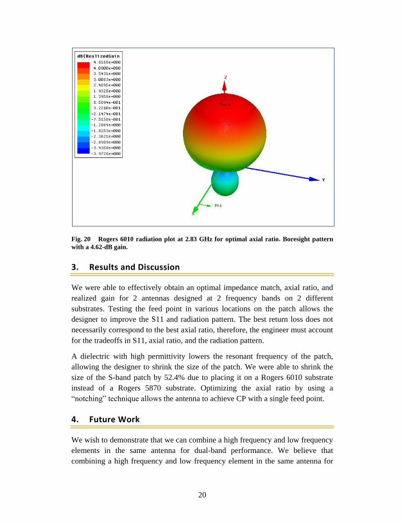
Figure 20 exhibits that the patch containing the Rogers 6010 substrate experiences
a 4.62-dB peak realized gain to boresight at 2.83 GHz for optimal axial ratio.
20
Fig. 20 Rogers 6010 radiation plot at 2.83 GHz for optimal axial ratio. Boresight pattern
with a 4.62-dB gain.
3. Results and Discussion
We were able to effectively obtain an optimal impedance match, axial ratio, and
realized gain for 2 antennas designed at 2 frequency bands on 2 different
substrates. Testing the feed point in various locations on the patch allows the
designer to improve the S11 and radiation pattern. The best return loss does not
necessarily correspond to the best axial ratio, therefore, the engineer must account
for the tradeoffs in S11, axial ratio, and the radiation pattern.
A dielectric with high permittivity lowers the resonant frequency of the patch,
allowing the designer to shrink the size of the patch. We were able to shrink the
size of the S-band patch by 52.4% due to placing it on a Rogers 6010 substrate
instead of a Rogers 5870 substrate. Optimizing the axial ratio by using a
“notching” technique allows the antenna to achieve CP with a single feed point.
4. Future Work
We wish to demonstrate that we can combine a high frequency and low frequency
elements in the same antenna for dual-band performance. We believe that
combining a high frequency and low frequency element in the same antenna for
21
dual-band performance will be an agile, adaptable, and cost-effective solution for
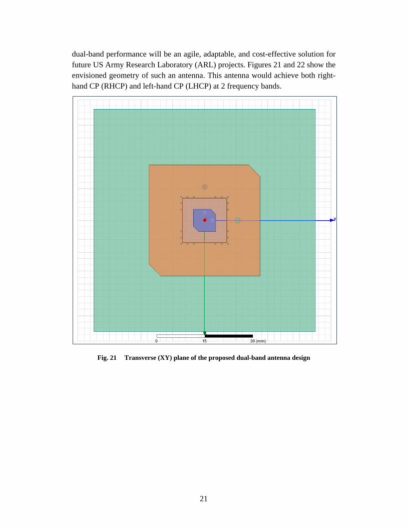
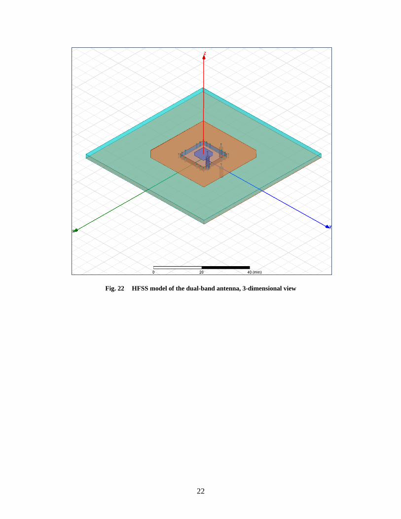
future US Army Research Laboratory (ARL) projects. Figures 21 and 22 show the
envisioned geometry of such an antenna. This antenna would achieve both right-
hand CP (RHCP) and left-hand CP (LHCP) at 2 frequency bands.
Fig. 21 Transverse (XY) plane of the proposed dual-band antenna design
22
Fig. 22 HFSS model of the dual-band antenna, 3-dimensional view

23
5. References
1. Breed G. The fundamentals of patch antenna design and performance. High
Frequency Electronics and Patch Antennas, Summit Technical Media, LLC,
2009.
2. Balanis C. Microstrip antenna. Antenna Theory, John Wiley & Sons Inc.,
2005.
3. Frenzel L. What’s the difference between a dipole and a ground plane
antenna? Electronic Design, July 2013. http://electronicdesign.com/wireless/
what-s-difference-between-dipole-and-ground-plane-antenna.
24
1 DEFENSE TECH INFO CTR
(PDF) DTIC OCA
2 US ARMY RSRCH LAB
(PDF) IMAL HRA MAIL & RECORDS MGMT
RDRL CIO LL TECHL LIB
1 GOVT PRNTG OFC
(PDF) A MALHOTRA
5 US ARMY RSRCH LAB
(PDF) RDRL SER M
G MITCHELL
A ZAGHLOUL
T ANTHONY
S WEISS
E ADLER