Embed Size (px)
Citation preview

DUBLIN CITY UNIVERSITY
SCHOOL OF ELECTRONIC ENGINEERING
Circularly Polarized Microstrip Antenna Array
Steafán Sherlock
April 2016
BACHELOR OF ENGINEERING
IN
ELECTRONIC SYSTEMS
Supervised by Dr. M. Condon

ii
ACKNOWLEDGEMENTS
I would like to thank my supervisor Dr. Marissa Condon for her guidance and
supervision over this project. I would also like to the Taoglas who made this
project possible with the use of their equipment and software. Lastly I would
like to thank the engineers in Taoglas and the technical staff in DCU for their
help and guidance throughout the course of this project.
DECLARATION
I declare that this material, which I now submit for assessment, is entirely my own work and
has not been taken from the work of others, save and to the extent that such work has been
cited and acknowledged within the text of my work. I understand that plagiarism, collusion,
and copying are grave and serious offences in the university and accept the penalties that
would be imposed should I engage in plagiarism, collusion or copying. I have read and
understood the Assignment Regulations set out in the module documentation. I have
identified and included the source of all facts, ideas, opinions, and viewpoints of others in the
assignment references. Direct quotations from books, journal articles, internet sources,
module text, or any other source whatsoever are acknowledged and the source cited are
identified in the assignment references. This assignment, or any part of it, has not been
previously submitted by me or any other person for assessment on this or any other course of
study.
I have read and understood the DCU Academic Integrity and Plagiarism at
https://www4.dcu.ie/sites/default/files/policy/1%20-
%20integrity_and_plagiarism_ovpaa_v3.pdf and IEEE referencing guidelines found at
https://loop.dcu.ie/mod/url/view.php?id=448779.
Name: ________________________________ Date: _________________

iii
ABSTRACT
CIRCULARLY POLARIZED MICROSTRIP ANTENNA ARRAY
STEAFÁN SHERLOCK
Polarization matching between transmitting and receiving antennas is important to minimise
transmission loss. Circularly polarized antennas are an attractive solution to the problem of
polarization mismatch in mobile devices. Circular polarization in an antenna reduces the
effect of multipath reflections, enhances weather penetration and allows mobility of both the
transmitting and receiving antenna.
This project proposes the design of a single fed circularly polarized microstrip antenna array
which operates at 2.4GHz. Microstrip antennas are lightweight, small volume and inexpensive
antennas. They can be mass produced using modern printed circuit board technologies. An
advantage of microstrip antennas is that they allow for linear and circular polarization.
Though with numerous advantages, microstrip antennas have the limitation of having a low
gain, which gives them low power handling capabilities. To overcome this limitation, a 2x2
array is introduced which improves antenna gain, directivity and efficiency.

iv
TABLE OF CONTENTS
Acknowledgements ................................................................................................................. ii
Declaration............................................................................................................................... ii
Abstract ................................................................................................................................... iii
Chapter 1 Introduction ....................................................................................................... 1
1.1 Aims and objectives .................................................................................................. 2
1.2 Report organisation ................................................................................................... 2
Chapter 2 Microstrip antennas ........................................................................................... 3
2.1 Advantages and disadvantages of microstrip antennas ............................................. 3
2.2 A microstrip antenna ................................................................................................. 4
2.2.1 Metallic patch .................................................................................................... 4
2.2.2 Dielectric substrate ............................................................................................ 4
2.2.3 The ground ......................................................................................................... 5
2.2.4 Feeding .............................................................................................................. 5
2.3 Polarization ............................................................................................................... 8
2.4 Circular polarization and microstrip antenna .......................................................... 10
2.5 Microstrip antenna arrays ....................................................................................... 10
2.6 Feed networks ......................................................................................................... 11
Chapter 3 Antenna Parameters ......................................................................................... 15
3.1 Fabrication and measurement equipment ............................................................... 15
3.1.1 Anechoic chamber ........................................................................................... 15
3.1.2 Network Analyser ............................................................................................ 16
3.1.3 Milling Machine .............................................................................................. 18
3.2 Return loss .............................................................................................................. 18
3.3 Radiation Pattern ..................................................................................................... 19
3.4 Efficiency ................................................................................................................ 20
3.5 Polarization ............................................................................................................. 20

v
3.6 Input Impedance ..................................................................................................... 21
3.7 Directivity and Gain ................................................................................................ 22
3.8 Summary ................................................................................................................. 23
Chapter 4 Design and simulation of a circularly polarized microstrip antenna array ...... 24
4.1 Design specifications .............................................................................................. 25
4.2 Single patch design with quarter wave transformer ................................................ 26
4.3 2x2 Array design with corporate feed network using T-junctions ......................... 28
4.4 Summary ................................................................................................................. 30
Chapter 5 Results and Discussion .................................................................................... 31
5.1 Single patch simulation results ............................................................................... 31
5.1.1 Return loss ....................................................................................................... 31
5.1.2 Directivity ........................................................................................................ 33
5.1.3 Gain ................................................................................................................. 34
5.1.4 Efficiency......................................................................................................... 35
5.1.5 Axial Ratio ....................................................................................................... 36
5.1.6 Radiation pattern ............................................................................................. 37
5.2 Antenna Array Simulation and measured results ................................................... 38
5.2.1 Return Loss ...................................................................................................... 38
5.2.2 Directivity ........................................................................................................ 40
5.2.3 Gain ................................................................................................................. 42
5.2.4 Efficiency......................................................................................................... 45
5.2.5 Axial Ratio ....................................................................................................... 47
5.2.6 Radiation Pattern ............................................................................................. 49
Chapter 6 Ethics ............................................................................................................... 51
6.1 The legal and ethical use of software ...................................................................... 51
6.2 Confidentiality with an external company .............................................................. 51
6.3 Health and safety .................................................................................................... 52
6.4 Testing .................................................................................................................... 52

vi
6.5 Conclusion .............................................................................................................. 53
Chapter 7 Conclusions ..................................................................................................... 54
References ............................................................................................................................. 56
Appendix ............................................................................................................................... 58

vii
Table of Figures Figure 2.1: Basic microstrip antenna structure [4]. ................................................................. 4
Figure 2.2: Metallic patch shapes [10]. ................................................................................... 4
Figure 2.3: Single and dual fed patch antennas [8]. ................................................................ 6
Figure 2.4: Microstrip antenna with side feed [2]. .................................................................. 6
Figure 2.5: Coaxial feed of a microstrip antenna [2]. .............................................................. 7
Figure 2.6: Proximity coupling feed of a microstrip antenna [2]. ........................................... 7
Figure 2.7: Aperture coupling feed of a microstrip antenna [2]. ............................................. 8
Figure 2.8: Types of polarization [4]. ...................................................................................... 9
Figure 2.9: Single feed CP patches [4]. ................................................................................. 10
Figure 2.10: Constructive and deconstructive interference [14]. .......................................... 11
Figure 2.11: Series feed and corporate feed networks [6]. .................................................... 12
Figure 2.12: Corporate-feed network with tapered lines [10]. .............................................. 12
Figure 2.13: Corporate-feed network with λ/4 transformers [10]. ........................................ 12
Figure 2.14: Lossless T-junction model [6]. ......................................................................... 13
Figure 2.15: λ/4 matching transformer [6]. ........................................................................... 14
Figure 3.1 Aligning antenna to centre point of measurement in the anechoic chamber with the
use of a laser .......................................................................................................................... 16
Figure 3.2: VNA .................................................................................................................... 17
Figure 3.3 Antenna fabrication using milling machine ......................................................... 18
Figure 3.4: Coordinate system for antenna analysis [10]. ..................................................... 19
Figure 3.5 Radiation pattern of a directional antenna [2]. ..................................................... 20
Figure 3.6: A transmission line terminated with a load [16]. ................................................ 21
Figure 3.7: Smith Chart [17].................................................................................................. 22
Figure 4.1: Physical and effective length of a microstrip patch [2]. ..................................... 26
Figure 4.2: Electric field lines [2]. ......................................................................................... 27
Figure 4.3 Single patch with 50Ω transmission line and quarter wave transformer. ............ 28
Figure 4.4 Isometric view of single patch antenna ................................................................ 28
Figure 4.5 Corporate feed network ........................................................................................ 29
Figure 4.6 Isometric view of 2x2 antenna array .................................................................... 30
Figure 5.1 Return loss for single patch .................................................................................. 32
Figure 5.2 Impedance view of single patch return loss ......................................................... 32
Figure 5.3 Directivity of single patch .................................................................................... 33
Figure 5.4 Peak gain of single patch ..................................................................................... 34

viii
Figure 5.5 Single patch efficiency ......................................................................................... 35
Figure 5.6 Axial ratio of single patch .................................................................................... 36
Figure 5.7 Radiation pattern of single patch.......................................................................... 37
Figure 5.8 Antenna array under measurement using a VNA and an anechoic chamber ....... 38
Figure 5.9 Antenna array return loss ..................................................................................... 39
Figure 5.10 Measured return loss of antenna array ............................................................... 40
Figure 5.11 Tuned antenna array prototype........................................................................... 40
Figure 5.12 Directivity of simulated antenna array ............................................................... 41
Figure 5.13 Measured directivity of antenna array ............................................................... 42
Figure 5.14 Peak gain of antenna array simulation ............................................................... 43
Figure 5.15 Measured antenna array peak gain ..................................................................... 44
Figure 5.16 Measured gain of antenna array ......................................................................... 44
Figure 5.17 Simulated antenna array efficiency .................................................................... 45
Figure 5.18Measured antenna array efficiency ..................................................................... 46
Figure 5.19 Axial ratio of simulated antenna array ............................................................... 47
Figure 5.20 Axial ratio of measured antenna array ............................................................... 48
Figure 5.21 Simulated antenna array radiation pattern.......................................................... 49
Figure 5.22 Measured antenna array radiation pattern .......................................................... 50
1
Chapter 1 INTRODUCTION
An antenna can be described as the part of a transmitting or receiving system that is designed
to radiate or to receive electromagnetic waves [1]. An antenna is a resonant device which is
tuned to operate efficiently over a relatively narrow frequency band [2]. In an ideal system,
an antenna should radiate all of the energy generated by the source. In a practical system,
there are losses due to impedance mismatch, transmission line losses and polarization losses,
which will be discussed in detail in Chapter 2. To avoid polarization mismatch, the
polarization of the transmitting antenna must be the same as that of the receiving antenna. For
this to happen, both of the antennas should have the same axial ratio, spatial orientation and
the same sense of polarization for maximum power transfer [3] [4]. In mobile and portable
wireless applications where the device orientation is constantly changing, it is nearly
impossible to match the spatial orientation of the two devices. Circular polarization (CP) of
the antennas can overcome this problem. Though circular polarization is more expensive and
difficult to achieve compared to linear polarization, it allows the transmitting or receiving
antenna to communicate with its opposite over a wide range of polarizations. This is because
the radiated electromagnetic waves oscillate in a circle which is perpendicular to the direction
of propagation [4] [5].
Many wireless applications require radiation characteristics that may not be achievable by a
single radiating element such as a highly directive antenna with a high gain. Rather than
increasing the size of a single radiating element, an aggregate of radiating elements in an
electrical and geometrical arrangement can be used to increase directivity and gain [6]. This
is also known as an array. This project is concerned with the design of a circularly polarized
microstrip antenna array which operates in the 2.4GHz range.
2.4GHz is the operation frequency for Wi-Fi which has become an everyday essential for
people in today’s society. Wi-Fi is now complimentary made available in most coffee shops,
shopping centres, buses, cinemas, hotels etc. The increasing demand for Wi-Fi increases the
demand for Wi-Fi antennas. This project focuses on the design of a directive Wi-Fi antenna
with a high gain to provide signal in a specific direction.

2
1.1 AIMS AND OBJECTIVES
The aim of this project is to design and fabricate a probe-fed, circularly polarized, microstrip
Wi-Fi antenna array. The fabricated antenna will then be tested to validate its performance.
The antenna should have directive, efficient, high gain and circular polarized characteristics.
1.2 REPORT ORGANISATION
Chapter 2 introduces the basic structure of a microstrip antenna. It discusses the advantages
and disadvantages of microstrip antennas as well as the different feeding techniques
commonly used. Circular polarization is explained and discussed in this chapter and how it
can be achieved in a microstrip antennas. The concept of antenna arrays are introduced along
with the feed networks and power dividers associated with them. Chapter 3 defines and the
parameters associated with antennas and to validate antenna performance. Chapter 4 outlines
the design process for the design of a single microstrip patch and the method used for its
expansion into a 2x2 antenna array. Chapter 5 discusses and criticizes the simulated and
measured antenna performance. The ethics surrounding this project and the conclusions
drawn are discussed in Chapter 6 and Chapter 7.
3
Chapter 2 MICROSTRIP ANTENNAS
The concept of a microstrip antenna (MSA) was first proposed by Deschamps in 1953, but it
wasn’t until the 1970s that practical antennas were developed by Munson and Howell [7]. A
MSA is a resonating antenna, usually designed for single mode operation, but can support
multiple modes [8]. In this chapter, we discuss the advantages and disadvantages of MSAs,
their basic structure, polarization and a number of different feed techniques.
2.1 ADVANTAGES AND DISADVANTAGES OF MICROSTRIP ANTENNAS
Microstrip antennas are lightweight, small volume, low profile antennas which can conform
to planar and non-planar surfaces. Their shape flexibility allows them to be mounted onto
rigid surfaces. This makes them mechanically robust. MSAs allow for dual and triple
frequency band operations, making them useful in a number of different applications such as
GSM, Wi-Fi, Bluetooth, and cellular. MSAs also allow for linear and circular polarization,
adding to their already numerous applications. They can be mass produced using inexpensive
modern printed circuit board (PCB) technologies such as a Milling machine. The use of these
PCB technologies also allows for the fabrication of the feeding and matching networks along
with the patch elements themselves. This results in a low fabrication cost making them
commercially appealable. A MSA provides a wide range of design options to accommodate
a consumer’s cost and performance objectives. A MSA designer can vary the substrate type,
type of perturbation, the feeding technique and the antenna structure to improve performance
or reduce cost. [9]
As well as having numerous advantages, MSAs have many limitations. MSAs feature a
narrow impedance bandwidth (1-5%), low efficiency and somewhat lower gain (~6dB) which
gives them low power-handling capabilities. They also show large ohmic losses in the feed
structure of arrays [9]. That being said, there are many ways which MSA performance can be
increased to counteract these limitations. Stacking the substrates and/or increasing substrate
height can broaden BW and increase efficiency [10]. MSAs also show poor polarization purity
and usually only radiate in half-space as they are usually implemented on double sided
laminates where one side is used as the ground. The research in MSAs mainly focuses on how
to overcome these limitations [4].
4
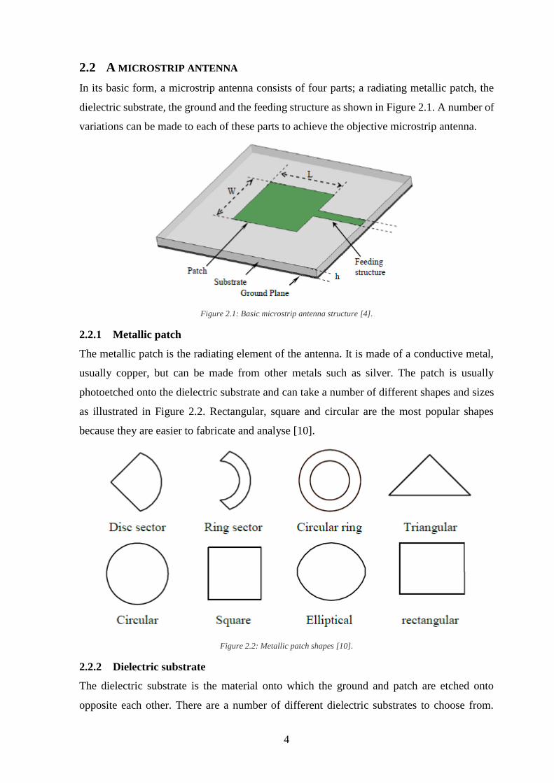
2.2 A MICROSTRIP ANTENNA
In its basic form, a microstrip antenna consists of four parts; a radiating metallic patch, the
dielectric substrate, the ground and the feeding structure as shown in Figure 2.1. A number of
variations can be made to each of these parts to achieve the objective microstrip antenna.
Figure 2.1: Basic microstrip antenna structure [4].
2.2.1 Metallic patch
The metallic patch is the radiating element of the antenna. It is made of a conductive metal,
usually copper, but can be made from other metals such as silver. The patch is usually
photoetched onto the dielectric substrate and can take a number of different shapes and sizes
as illustrated in Figure 2.2. Rectangular, square and circular are the most popular shapes
because they are easier to fabricate and analyse [10].
Figure 2.2: Metallic patch shapes [10].
2.2.2 Dielectric substrate
The dielectric substrate is the material onto which the ground and patch are etched onto
opposite each other. There are a number of different dielectric substrates to choose from.

5
Substrate thickness, dielectric constant and the price are the factors which most influence the
substrate choice. Dielectric constants in substrates usually range from 2.2 ≤ εr ≤ 12, which is
the relative permittivity of the material [10]. A thick substrate and a low dielectric constant
is desirable to achieve a broad bandwidth, due to the substrate thickness being directionally
proportional to the MSA BW, and this also leads to better efficiency [10] [7]. For low-cost
antenna prototypes, inexpensive glass-epoxy substrates are used such as FR-4, with εr ≈ 4.3
[7].
2.2.3 The ground
The ground is made from the same conductive metal as the patch and it is situated on the
opposite side of the dielectric substrate. The ground plane is part of the antenna. The ground
plane can be increased to improve antenna performance (usually antenna efficiency), but this
increase in performance is limited and will ‘level off’ once the performance peak is reached.
The radiation of the antenna is generated by the fringing field between the patch and the
ground plane [11].
2.2.4 Feeding
There are many different types of feeding methods for microstrip antennas. A patch antenna
can be fed by a single feed or multiple feeds as shown in Figure 2.3. Feed techniques can also
be categorised as contacting and non-contacting. Popular contacting techniques include
microstrip line feed and coaxial line feed where, the RF power is directly fed to the radiating
patch from the connecting element (microstrip feed line, coaxial line, etc.). Popular non-
contacting techniques include aperture coupling and proximity coupling, where
electromagnetic field coupling transfers power between the microstrip line and the radiating
patch [8].
6
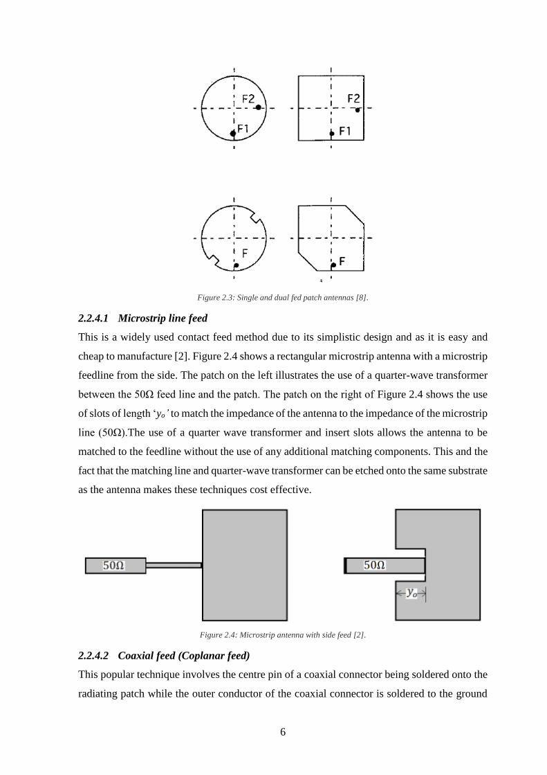
Figure 2.3: Single and dual fed patch antennas [8].
2.2.4.1 Microstrip line feed
This is a widely used contact feed method due to its simplistic design and as it is easy and
cheap to manufacture [2]. Figure 2.4 shows a rectangular microstrip antenna with a microstrip
feedline from the side. The patch on the left illustrates the use of a quarter-wave transformer
between the 50Ω feed line and the patch. The patch on the right of Figure 2.4 shows the use
of slots of length ‘yo’ to match the impedance of the antenna to the impedance of the microstrip
line (50Ω).The use of a quarter wave transformer and insert slots allows the antenna to be
matched to the feedline without the use of any additional matching components. This and the
fact that the matching line and quarter-wave transformer can be etched onto the same substrate
as the antenna makes these techniques cost effective.
Figure 2.4: Microstrip antenna with side feed [2].
2.2.4.2 Coaxial feed (Coplanar feed)
This popular technique involves the centre pin of a coaxial connector being soldered onto the
radiating patch while the outer conductor of the coaxial connector is soldered to the ground
7
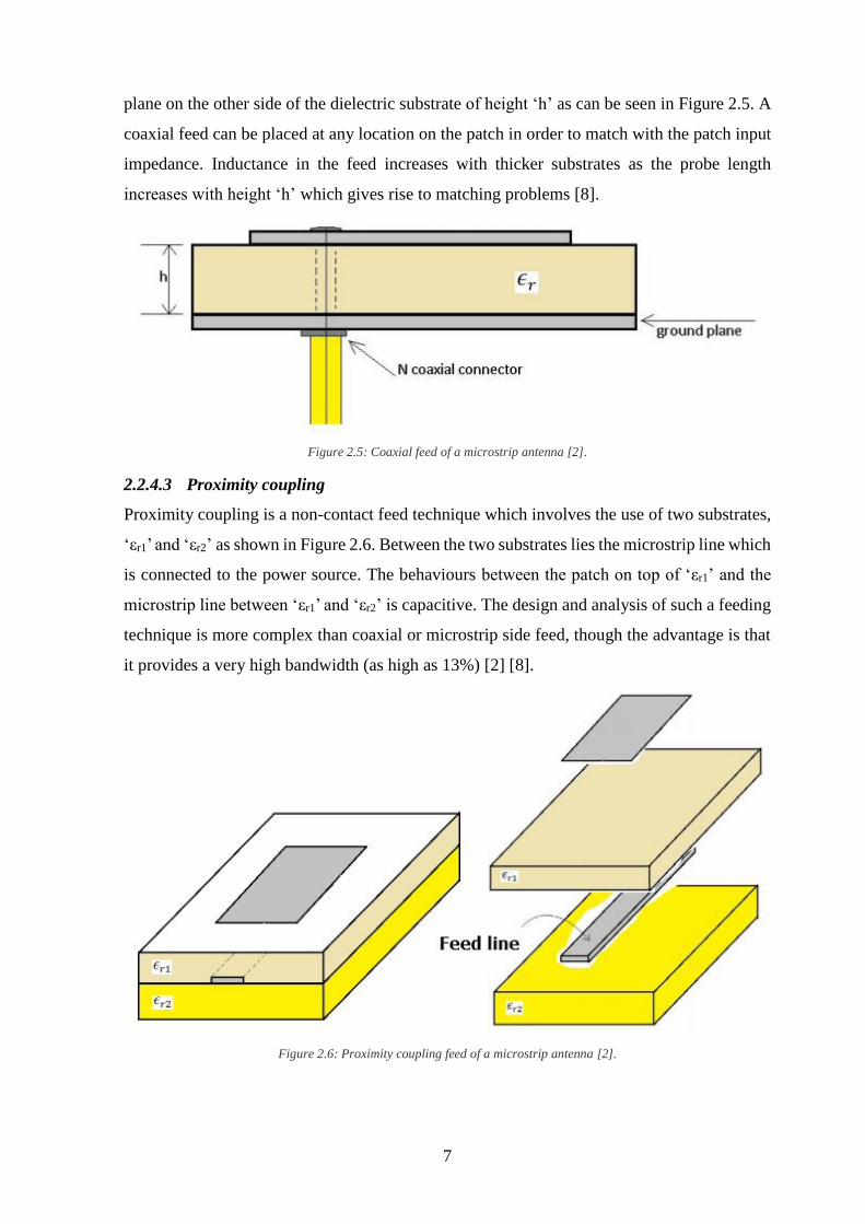
plane on the other side of the dielectric substrate of height ‘h’ as can be seen in Figure 2.5. A
coaxial feed can be placed at any location on the patch in order to match with the patch input
impedance. Inductance in the feed increases with thicker substrates as the probe length
increases with height ‘h’ which gives rise to matching problems [8].
Figure 2.5: Coaxial feed of a microstrip antenna [2].
2.2.4.3 Proximity coupling
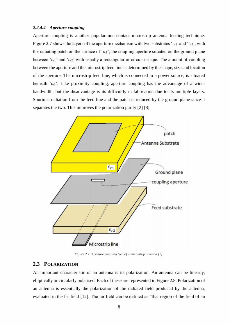
Proximity coupling is a non-contact feed technique which involves the use of two substrates,
‘εr1’ and ‘εr2’ as shown in Figure 2.6. Between the two substrates lies the microstrip line which
is connected to the power source. The behaviours between the patch on top of ‘εr1’ and the
microstrip line between ‘εr1’ and ‘εr2’ is capacitive. The design and analysis of such a feeding
technique is more complex than coaxial or microstrip side feed, though the advantage is that
it provides a very high bandwidth (as high as 13%) [2] [8].
Figure 2.6: Proximity coupling feed of a microstrip antenna [2].
8
2.2.4.4 Aperture coupling
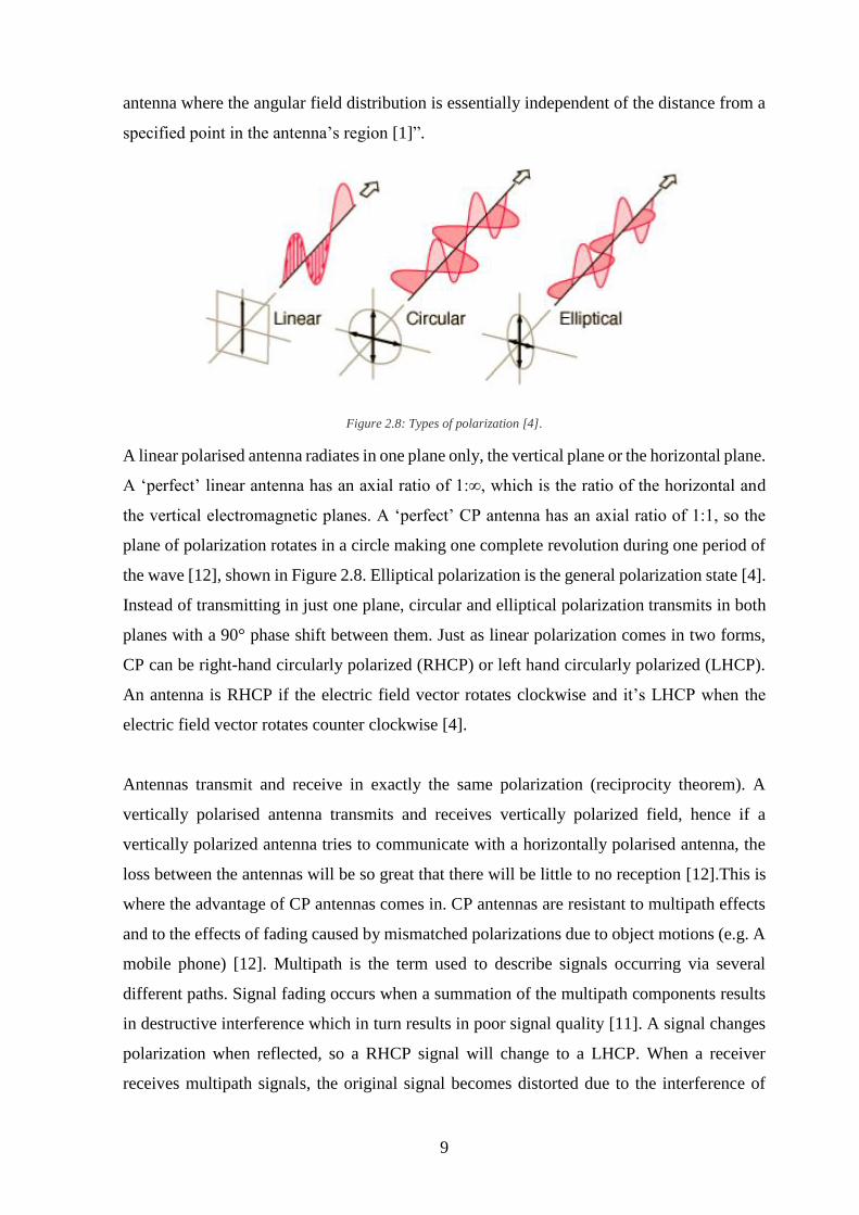
Aperture coupling is another popular non-contact microstrip antenna feeding technique.
Figure 2.7 shows the layers of the aperture mechanism with two substrates ‘εr1’ and ‘εr2’, with
the radiating patch on the surface of ‘εr1’, the coupling aperture situated on the ground plane
between ‘εr1’ and ‘εr2’ with usually a rectangular or circular shape. The amount of coupling
between the aperture and the microstrip feed line is determined by the shape, size and location
of the aperture. The microstrip feed line, which is connected to a power source, is situated
beneath ‘εr2’. Like proximity coupling, aperture coupling has the advantage of a wider
bandwidth, but the disadvantage is its difficultly in fabrication due to its multiple layers.
Spurious radiation from the feed line and the patch is reduced by the ground plane since it
separates the two. This improves the polarization purity [2] [8].
Figure 2.7: Aperture coupling feed of a microstrip antenna [2].
2.3 POLARIZATION
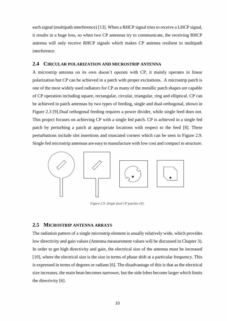
An important characteristic of an antenna is its polarization. An antenna can be linearly,
elliptically or circularly polarised. Each of these are represented in Figure 2.8. Polarization of
an antenna is essentially the polarization of the radiated field produced by the antenna,
evaluated in the far field [12]. The far field can be defined as “that region of the field of an
9
antenna where the angular field distribution is essentially independent of the distance from a
specified point in the antenna’s region [1]”.
Figure 2.8: Types of polarization [4].
A linear polarised antenna radiates in one plane only, the vertical plane or the horizontal plane.
A ‘perfect’ linear antenna has an axial ratio of 1:∞, which is the ratio of the horizontal and
the vertical electromagnetic planes. A ‘perfect’ CP antenna has an axial ratio of 1:1, so the
plane of polarization rotates in a circle making one complete revolution during one period of
the wave [12], shown in Figure 2.8. Elliptical polarization is the general polarization state [4].
Instead of transmitting in just one plane, circular and elliptical polarization transmits in both
planes with a 90° phase shift between them. Just as linear polarization comes in two forms,
CP can be right-hand circularly polarized (RHCP) or left hand circularly polarized (LHCP).
An antenna is RHCP if the electric field vector rotates clockwise and it’s LHCP when the
electric field vector rotates counter clockwise [4].
Antennas transmit and receive in exactly the same polarization (reciprocity theorem). A
vertically polarised antenna transmits and receives vertically polarized field, hence if a
vertically polarized antenna tries to communicate with a horizontally polarised antenna, the
loss between the antennas will be so great that there will be little to no reception [12].This is
where the advantage of CP antennas comes in. CP antennas are resistant to multipath effects
and to the effects of fading caused by mismatched polarizations due to object motions (e.g. A
mobile phone) [12]. Multipath is the term used to describe signals occurring via several
different paths. Signal fading occurs when a summation of the multipath components results
in destructive interference which in turn results in poor signal quality [11]. A signal changes
polarization when reflected, so a RHCP signal will change to a LHCP. When a receiver
receives multipath signals, the original signal becomes distorted due to the interference of
10
each signal (multipath interference) [13]. When a RHCP signal tries to receive a LHCP signal,
it results in a huge loss, so when two CP antennas try to communicate, the receiving RHCP
antenna will only receive RHCP signals which makes CP antenna resilient to multipath
interference.
2.4 CIRCULAR POLARIZATION AND MICROSTRIP ANTENNA
A microstrip antenna on its own doesn’t operate with CP, it mainly operates in linear
polarization but CP can be achieved in a patch with proper excitations. A microstrip patch is
one of the most widely used radiators for CP as many of the metallic patch shapes are capable
of CP operation including square, rectangular, circular, triangular, ring and elliptical. CP can
be achieved in patch antennas by two types of feeding, single and dual-orthogonal, shown in
Figure 2.3 [9].Dual orthogonal feeding requires a power divider, while single feed does not.
This project focuses on achieving CP with a single fed patch. CP is achieved in a single fed
patch by perturbing a patch at appropriate locations with respect to the feed [8]. These
perturbations include slot insertions and truncated corners which can be seen in Figure 2.9.
Single fed microstrip antennas are easy to manufacture with low cost and compact in structure.
Figure 2.9: Single feed CP patches [4].
2.5 MICROSTRIP ANTENNA ARRAYS
The radiation pattern of a single microstrip element is usually relatively wide, which provides
low directivity and gain values (Antenna measurement values will be discussed in Chapter 3).
In order to get high directivity and gain, the electrical size of the antenna must be increased
[10], where the electrical size is the size in terms of phase shift at a particular frequency. This
is expressed in terms of degrees or radians [6]. The disadvantage of this is that as the electrical
size increases, the main bean becomes narrower, but the side lobes become larger which limits
the directivity [6].
11
Another way to increase the gain and directive characteristics of an antenna is to form an
assembly of radiating elements, which is called an array. This method doesn’t require the
increase in size of the individual elements. The total field of the array is given by the vector
addition of the fields of the individual elements. The elements of an array are usually identical
and their individual fields interfere constructively in the desired direction and destructively in
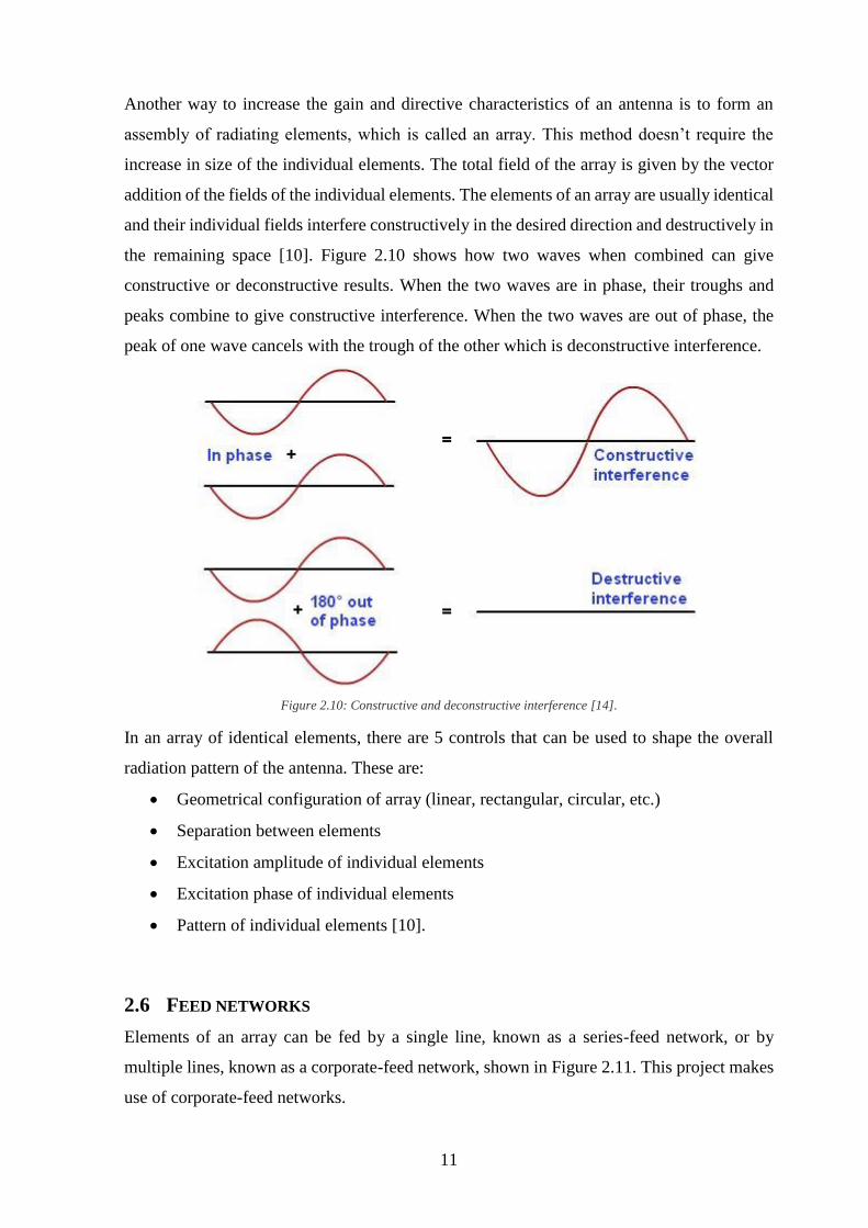
the remaining space [10]. Figure 2.10 shows how two waves when combined can give
constructive or deconstructive results. When the two waves are in phase, their troughs and
peaks combine to give constructive interference. When the two waves are out of phase, the
peak of one wave cancels with the trough of the other which is deconstructive interference.
Figure 2.10: Constructive and deconstructive interference [14].
In an array of identical elements, there are 5 controls that can be used to shape the overall
radiation pattern of the antenna. These are:
Geometrical configuration of array (linear, rectangular, circular, etc.)
Separation between elements
Excitation amplitude of individual elements
Excitation phase of individual elements
Pattern of individual elements [10].
2.6 FEED NETWORKS
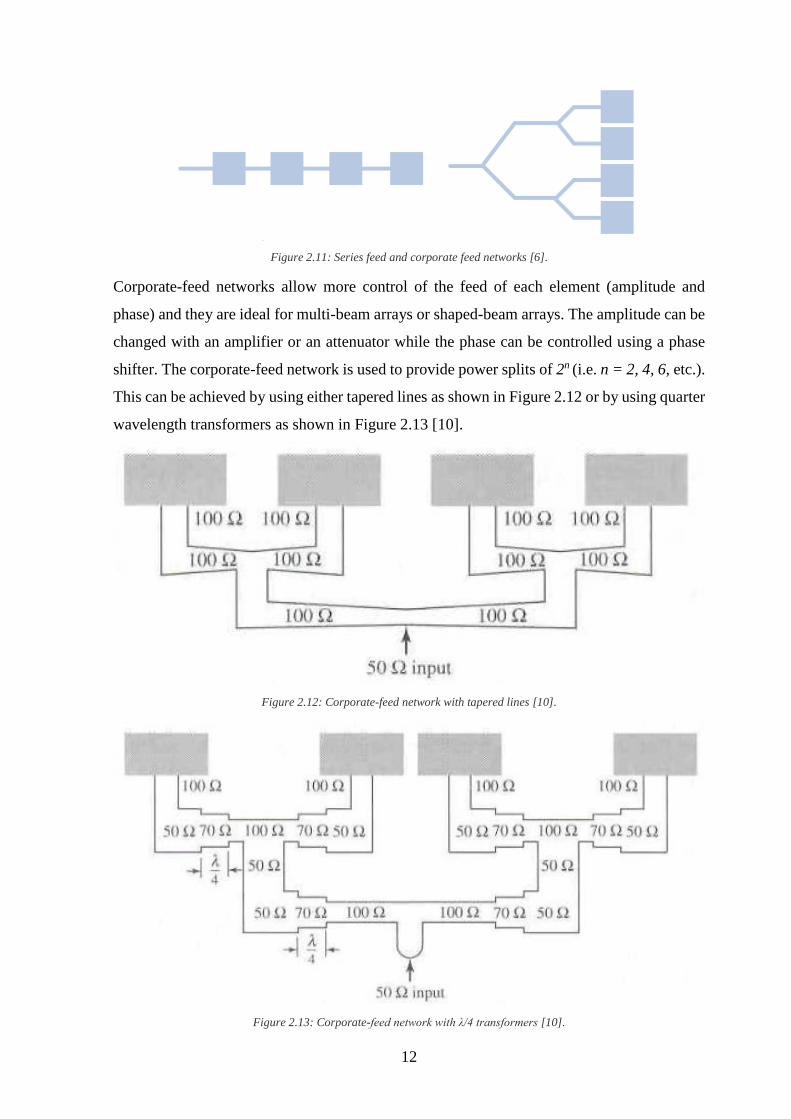
Elements of an array can be fed by a single line, known as a series-feed network, or by
multiple lines, known as a corporate-feed network, shown in Figure 2.11. This project makes
use of corporate-feed networks.
12
Figure 2.11: Series feed and corporate feed networks [6].
Corporate-feed networks allow more control of the feed of each element (amplitude and
phase) and they are ideal for multi-beam arrays or shaped-beam arrays. The amplitude can be
changed with an amplifier or an attenuator while the phase can be controlled using a phase
shifter. The corporate-feed network is used to provide power splits of 2n (i.e. n = 2, 4, 6, etc.).
This can be achieved by using either tapered lines as shown in Figure 2.12 or by using quarter
wavelength transformers as shown in Figure 2.13 [10].
Figure 2.12: Corporate-feed network with tapered lines [10].
Figure 2.13: Corporate-feed network with λ/4 transformers [10].
13
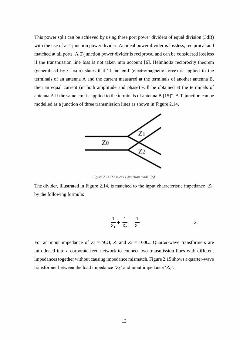
This power split can be achieved by using three port power dividers of equal division (3dB)
with the use of a T-junction power divider. An ideal power divider is lossless, reciprocal and
matched at all ports. A T-junction power divider is reciprocal and can be considered lossless
if the transmission line loss is not taken into account [6]. Helmholtz reciprocity theorem
(generalised by Carson) states that “If an emf (electromagnetic force) is applied to the
terminals of an antenna A and the current measured at the terminals of another antenna B,
then an equal current (in both amplitude and phase) will be obtained at the terminals of
antenna A if the same emf is applied to the terminals of antenna B [15]”. A T-junction can be
modelled as a junction of three transmission lines as shown in Figure 2.14.
Figure 2.14: Lossless T-junction model [6].
The divider, illustrated in Figure 2.14, is matched to the input characteristic impedance ‘Z0’
by the following formula:
1
𝑍1+
1
𝑍2=
1
𝑍0 2.1
For an input impedance of Z0 = 50Ω, Z1 and Z2 = 100Ω. Quarter-wave transformers are
introduced into a corporate-feed network to connect two transmission lines with different
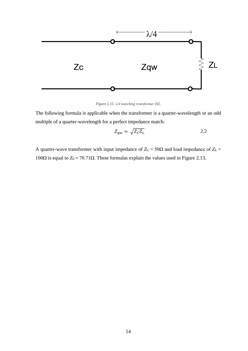
impedances together without causing impedance mismatch. Figure 2.15 shows a quarter-wave
transformer between the load impedance ‘ZL’ and input impedance ‘ZC’.
14
Figure 2.15: λ/4 matching transformer [6].
The following formula is applicable when the transformer is a quarter-wavelength or an odd
multiple of a quarter-wavelength for a perfect impedance match:
𝑍𝑞𝑤 = √𝑍𝐶𝑍𝐿 2.2
A quarter-wave transformer with input impedance of ZC = 50Ω and load impedance of ZL =
100Ω is equal to Z0 = 70.71Ω. These formulas explain the values used in Figure 2.13.

15
Chapter 3 ANTENNA PARAMETERS
An antenna, once designed and constructed, must be validated using the proper
measurements. Typical measurements include gain, directivity, axial ratio, radiation pattern
and efficiency. In this chapter, we discuss the different antenna measurements and the
equipment used to measure them.
3.1 FABRICATION AND MEASUREMENT EQUIPMENT
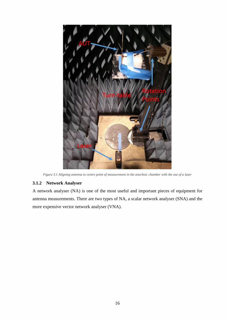
3.1.1 Anechoic chamber
An anechoic chamber allows the measurement of antenna properties indoors by preventing
reflections/echoes and by preventing external interference due to its metallic exterior. The
chamber minimizes reflections of electromagnetic waves from walls over a wide range of
incident angles and frequencies [11]. The chamber used for the testing of the antenna array
prototype is of a tapered shape. The source antenna is at one end of the chamber and the
antenna under test (AUT) is at the other end. The AUT is fixed to a podium which is on top
of a turn table. When measuring, the AUT is rotation about two axes at usually 5° increments.
The rotation points can be seen in Figure 3.1. The AUT is rotated by 360° in both the theta
and phi directions to gain a full measurement of the antenna. Theta and phi refer to spherical
coordinates which are used in the design and measurement of the antenna. A laser is needed
to align the AUT to the centre point of measurement in the chamber as seen in Figure 3.1.
16
Figure 3.1 Aligning antenna to centre point of measurement in the anechoic chamber with the use of a laser
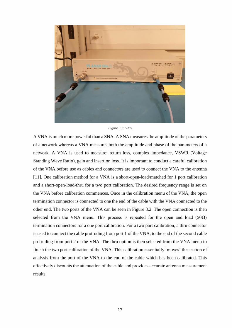
3.1.2 Network Analyser
A network analyser (NA) is one of the most useful and important pieces of equipment for
antenna measurements. There are two types of NA, a scalar network analyser (SNA) and the
more expensive vector network analyser (VNA).
17
Figure 3.2: VNA
A VNA is much more powerful than a SNA. A SNA measures the amplitude of the parameters
of a network whereas a VNA measures both the amplitude and phase of the parameters of a
network. A VNA is used to measure: return loss, complex impedance, VSWR (Voltage
Standing Wave Ratio), gain and insertion loss. It is important to conduct a careful calibration
of the VNA before use as cables and connectors are used to connect the VNA to the antenna
[11]. One calibration method for a VNA is a short-open-load/matched for 1 port calibration
and a short-open-load-thru for a two port calibration. The desired frequency range is set on
the VNA before calibration commences. Once in the calibration menu of the VNA, the open
termination connector is connected to one the end of the cable with the VNA connected to the
other end. The two ports of the VNA can be seen in Figure 3.2. The open connection is then
selected from the VNA menu. This process is repeated for the open and load (50Ω)
termination connectors for a one port calibration. For a two port calibration, a thru connector
is used to connect the cable protruding from port 1 of the VNA, to the end of the second cable
protruding from port 2 of the VNA. The thru option is then selected from the VNA menu to
finish the two port calibration of the VNA. This calibration essentially ‘moves’ the section of
analysis from the port of the VNA to the end of the cable which has been calibrated. This
effectively discounts the attenuation of the cable and provides accurate antenna measurement
results.
18
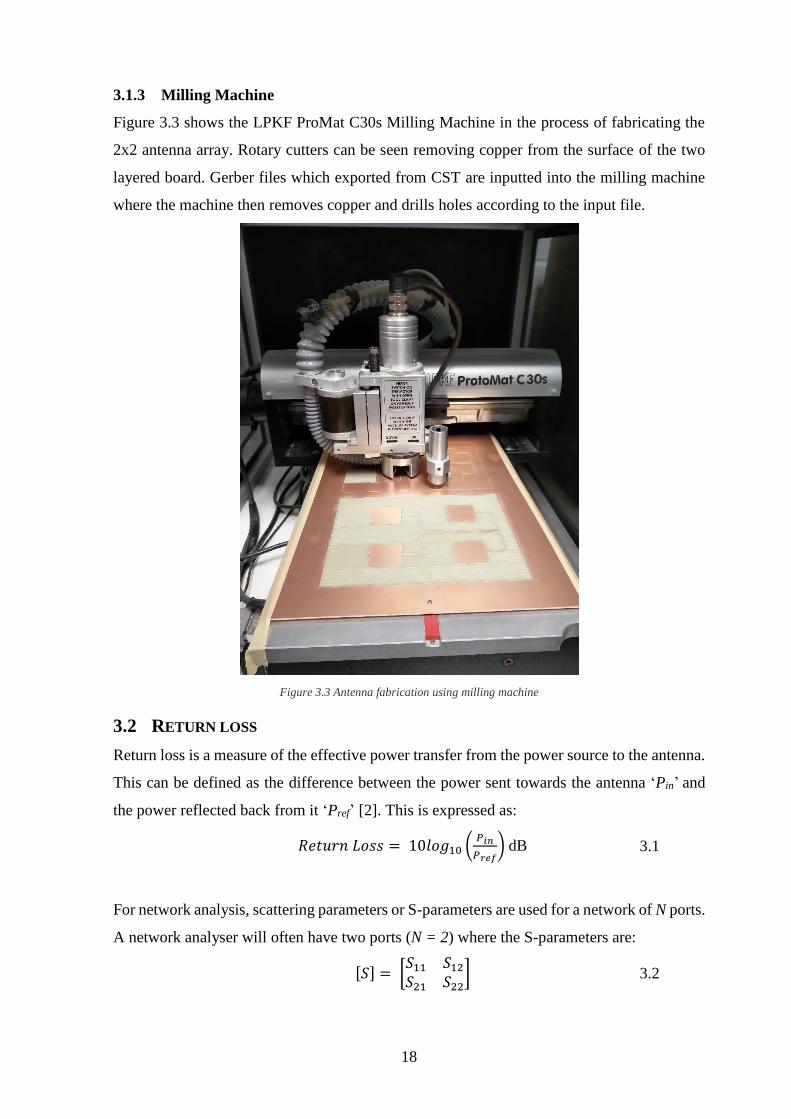
3.1.3 Milling Machine
Figure 3.3 shows the LPKF ProMat C30s Milling Machine in the process of fabricating the
2x2 antenna array. Rotary cutters can be seen removing copper from the surface of the two
layered board. Gerber files which exported from CST are inputted into the milling machine
where the machine then removes copper and drills holes according to the input file.
Figure 3.3 Antenna fabrication using milling machine
3.2 RETURN LOSS
Return loss is a measure of the effective power transfer from the power source to the antenna.
This can be defined as the difference between the power sent towards the antenna ‘Pin’ and
the power reflected back from it ‘Pref’ [2]. This is expressed as:
𝑅𝑒𝑡𝑢𝑟𝑛 𝐿𝑜𝑠𝑠 = 10𝑙𝑜𝑔10 (𝑃𝑖𝑛
𝑃𝑟𝑒𝑓) dB 3.1
For network analysis, scattering parameters or S-parameters are used for a network of N ports.
A network analyser will often have two ports (N = 2) where the S-parameters are:
[𝑆] = [𝑆11 𝑆12
𝑆21 𝑆22] 3.2
19
Table 3-1: Scatter Parameters
S11 Port 1 reflective coefficient
S12 Port 2 to Port 1 transmission coefficient
S21 Port 1 to Port 2 transmission coefficient
S22 Port 2 reflective coefficient
The reciprocity principal is generally understood to hold between S12 and S21 so that S12 ≈ S21.
These transmission coefficients indicate the isolation between two antennas. S11 and S22 (the
reflective coefficients) indicate how well the antenna feed line is matched with the antenna
[11]. Return loss can also be written in terms of the reflective coefficient:
𝑅𝑒𝑡𝑢𝑟𝑛 𝐿𝑜𝑠𝑠 = |20𝑙𝑜𝑔10|𝑆11|| dB 3.3
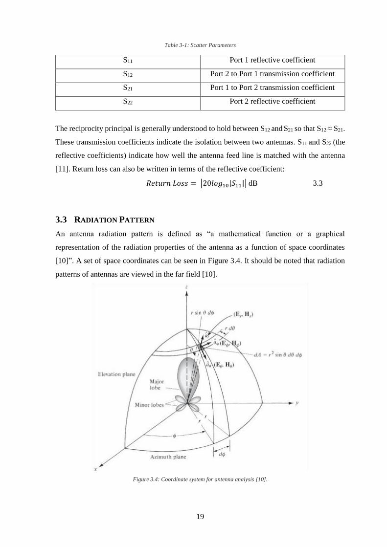
3.3 RADIATION PATTERN
An antenna radiation pattern is defined as “a mathematical function or a graphical
representation of the radiation properties of the antenna as a function of space coordinates
[10]”. A set of space coordinates can be seen in Figure 3.4. It should be noted that radiation
patterns of antennas are viewed in the far field [10].
Figure 3.4: Coordinate system for antenna analysis [10].
20
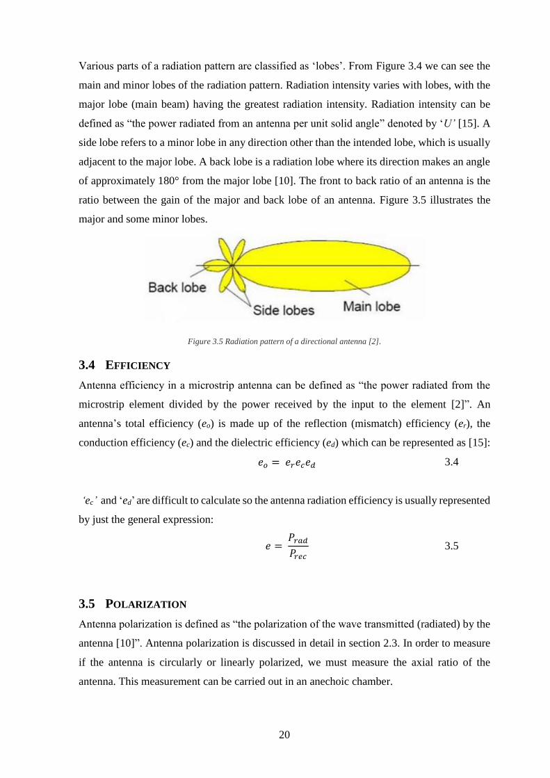
Various parts of a radiation pattern are classified as ‘lobes’. From Figure 3.4 we can see the
main and minor lobes of the radiation pattern. Radiation intensity varies with lobes, with the
major lobe (main beam) having the greatest radiation intensity. Radiation intensity can be
defined as “the power radiated from an antenna per unit solid angle” denoted by ‘U’ [15]. A
side lobe refers to a minor lobe in any direction other than the intended lobe, which is usually
adjacent to the major lobe. A back lobe is a radiation lobe where its direction makes an angle
of approximately 180° from the major lobe [10]. The front to back ratio of an antenna is the
ratio between the gain of the major and back lobe of an antenna. Figure 3.5 illustrates the
major and some minor lobes.
Figure 3.5 Radiation pattern of a directional antenna [2].
3.4 EFFICIENCY
Antenna efficiency in a microstrip antenna can be defined as “the power radiated from the
microstrip element divided by the power received by the input to the element [2]”. An
antenna’s total efficiency (eo) is made up of the reflection (mismatch) efficiency (er), the
conduction efficiency (ec) and the dielectric efficiency (ed) which can be represented as [15]:
𝑒𝑜 = 𝑒𝑟𝑒𝑐𝑒𝑑 3.4
‘ec’ and ‘ed’ are difficult to calculate so the antenna radiation efficiency is usually represented
by just the general expression:
𝑒 = 𝑃𝑟𝑎𝑑
𝑃𝑟𝑒𝑐 3.5
3.5 POLARIZATION
Antenna polarization is defined as “the polarization of the wave transmitted (radiated) by the
antenna [10]”. Antenna polarization is discussed in detail in section 2.3. In order to measure
if the antenna is circularly or linearly polarized, we must measure the axial ratio of the
antenna. This measurement can be carried out in an anechoic chamber.
21
3.6 INPUT IMPEDANCE
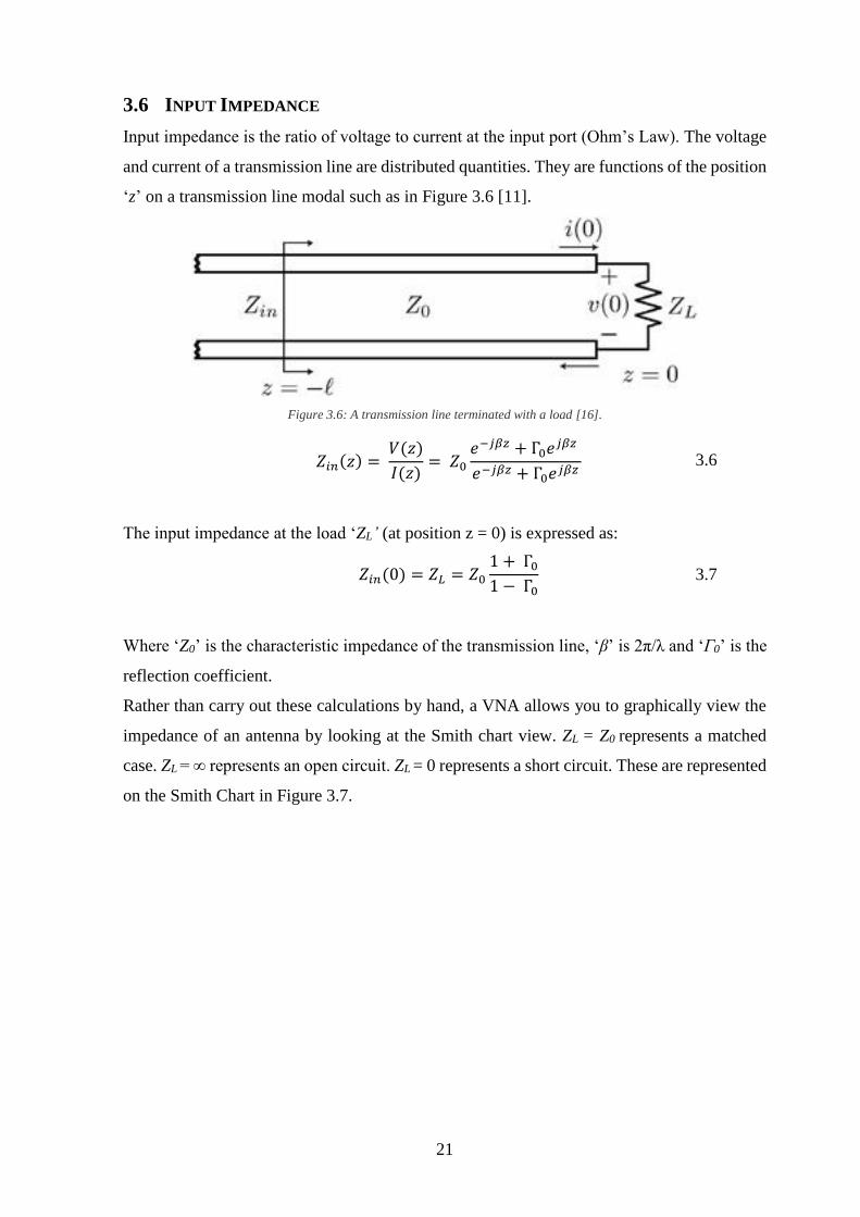
Input impedance is the ratio of voltage to current at the input port (Ohm’s Law). The voltage
and current of a transmission line are distributed quantities. They are functions of the position
‘z’ on a transmission line modal such as in Figure 3.6 [11].
Figure 3.6: A transmission line terminated with a load [16].
𝑍𝑖𝑛(𝑧) = 𝑉(𝑧)
𝐼(𝑧)= 𝑍0
𝑒−𝑗𝛽𝑧 + Γ0𝑒𝑗𝛽𝑧
𝑒−𝑗𝛽𝑧 + Γ0𝑒𝑗𝛽𝑧 3.6
The input impedance at the load ‘ZL’ (at position z = 0) is expressed as:
𝑍𝑖𝑛(0) = 𝑍𝐿 = 𝑍0
1 + Γ0
1 − Γ0 3.7
Where ‘Z0’ is the characteristic impedance of the transmission line, ‘β’ is 2π/λ and ‘Г0’ is the
reflection coefficient.
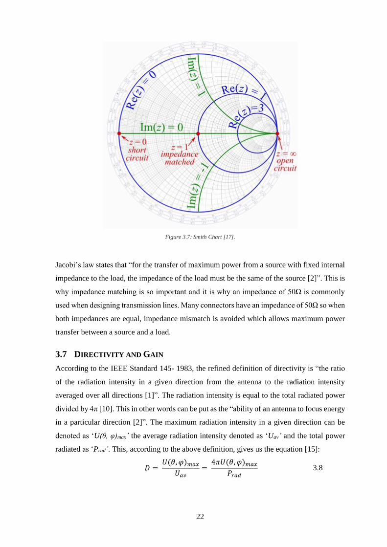
Rather than carry out these calculations by hand, a VNA allows you to graphically view the
impedance of an antenna by looking at the Smith chart view. ZL = Z0 represents a matched
case. ZL = ∞ represents an open circuit. ZL = 0 represents a short circuit. These are represented
on the Smith Chart in Figure 3.7.
22
Figure 3.7: Smith Chart [17].
Jacobi’s law states that “for the transfer of maximum power from a source with fixed internal
impedance to the load, the impedance of the load must be the same of the source [2]”. This is
why impedance matching is so important and it is why an impedance of 50Ω is commonly
used when designing transmission lines. Many connectors have an impedance of 50Ω so when
both impedances are equal, impedance mismatch is avoided which allows maximum power
transfer between a source and a load.
3.7 DIRECTIVITY AND GAIN
According to the IEEE Standard 145- 1983, the refined definition of directivity is “the ratio
of the radiation intensity in a given direction from the antenna to the radiation intensity
averaged over all directions [1]”. The radiation intensity is equal to the total radiated power
divided by 4π [10]. This in other words can be put as the “ability of an antenna to focus energy
in a particular direction [2]”. The maximum radiation intensity in a given direction can be
denoted as ‘U(θ, φ)max’ the average radiation intensity denoted as ‘Uav’ and the total power
radiated as ‘Prad’. This, according to the above definition, gives us the equation [15]:
𝐷 = 𝑈(𝜃, 𝜑)𝑚𝑎𝑥
𝑈𝑎𝑣=
4𝜋𝑈(𝜃, 𝜑)𝑚𝑎𝑥
𝑃𝑟𝑎𝑑 3.8

23
According to the IEEE Standard 145- 1983, directive gain can be defined as “the ratio of the
radiation intensity, in a given direction to the radiation intensity that would be obtained if the
power accepted by the antenna were radiated isotropically [1]”. Isotropic radiation refers to
equal radiation in all directions [15]. We obtain gain from the directivity of the antenna from
the equation:
𝐺 = 𝑒𝐷 3.9
‘e’ is the efficiency of the antenna which valued between 0 and 1 so the gain of the antenna
will always be less than the directivity unless efficiency is equal to 100%. Directivity is
independent of antenna loss and mismatch, while antenna gain takes these factors into account
[15].
3.8 SUMMARY
This chapter defined the antenna parameters return loss, directivity, gain, radiation pattern,
efficiency polarization and impedance which will be measured and discussed in Chapter 5.
The measurement equipment which was used to measure the antenna array prototype was also
introduced.

24
Chapter 4 DESIGN AND SIMULATION OF A CIRCULARLY
POLARIZED MICROSTRIP ANTENNA ARRAY
This chapter describes the design and simulation of a single CP radiating patch using the
design methodology outlined in the books by Balanis: “Antenna Theory and Design” [10] and
“Antennas from theory to practice” by Huang and Boyle [11]. All calculations were done
using Matlab which can be seen in the Appendix. The simulation software used is CST
(Computer Simulation Technology).
4.1 CST MICROWAVE STUDIO
This project makes use of the transient solver in CST. The transient solver or time domain
solver in CST is a general purpose 3D electromagnetic (EM) simulator. All EM solvers are
based on solving Maxwell’s equations in different forms. The transient solver in CST is based
on the finite integration technique (FIT). This technique is a consistent discretization scheme
for Maxwell’s equations in their integral form [18]. This discrete reformulation of Maxwell’s
equations in their integral form allows CST to simulate real-world EM field problems with
complex geometries [18].
The geometrical model of the antenna is divided into hexahedra where the number of mesh
cells can be adjusted to reduce simulation time (decrease) or to improve accuracy (increase).
The hexahedra mesh view can be seen in Figure 4.1. The time signal is then propagated
through the antenna structure. The hexahedra mesh is a very robust was of meshing for
complicated structures with the exception of curved geometries. The hexahedra must be
extremely dense for these geometries and so simulation time increases [19]. This project does
not make use of a curved geometrical structure so the transient solver with hexahedra mesh is
a suitable EM simulator for the antenna design presented in this chapter.
25
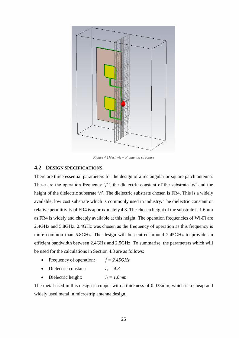
Figure 4.1Mesh view of antenna structure
4.2 DESIGN SPECIFICATIONS
There are three essential parameters for the design of a rectangular or square patch antenna.
These are the operation frequency ‘f’’, the dielectric constant of the substrate ‘εr’ and the
height of the dielectric substrate ‘h’. The dielectric substrate chosen is FR4. This is a widely
available, low cost substrate which is commonly used in industry. The dielectric constant or
relative permittivity of FR4 is approximately 4.3. The chosen height of the substrate is 1.6mm
as FR4 is widely and cheaply available at this height. The operation frequencies of Wi-Fi are
2.4GHz and 5.8GHz. 2.4GHz was chosen as the frequency of operation as this frequency is
more common than 5.8GHz. The design will be centred around 2.45GHz to provide an
efficient bandwidth between 2.4GHz and 2.5GHz. To summarise, the parameters which will
be used for the calculations in Section 4.3 are as follows:
Frequency of operation: f = 2.45GHz
Dielectric constant: εr = 4.3
Dielectric height: h = 1.6mm
The metal used in this design is copper with a thickness of 0.033mm, which is a cheap and
widely used metal in microstrip antenna design.
26
4.3 SINGLE PATCH DESIGN WITH QUARTER WAVE TRANSFORMER
From equation 4.1 we calculate W, the width of the antenna:
𝑊 = 1
2𝑓√𝜇0𝜀0
√2
𝜀𝑟 + 1 4.1
Using W, we determine the effective constant of the patch antenna using equation 4.2:
𝜀𝑟𝑒𝑓𝑓 =
𝜀𝑟 + 1
2+
𝜀𝑟 − 1
2√1 +12ℎ𝑊
4.2
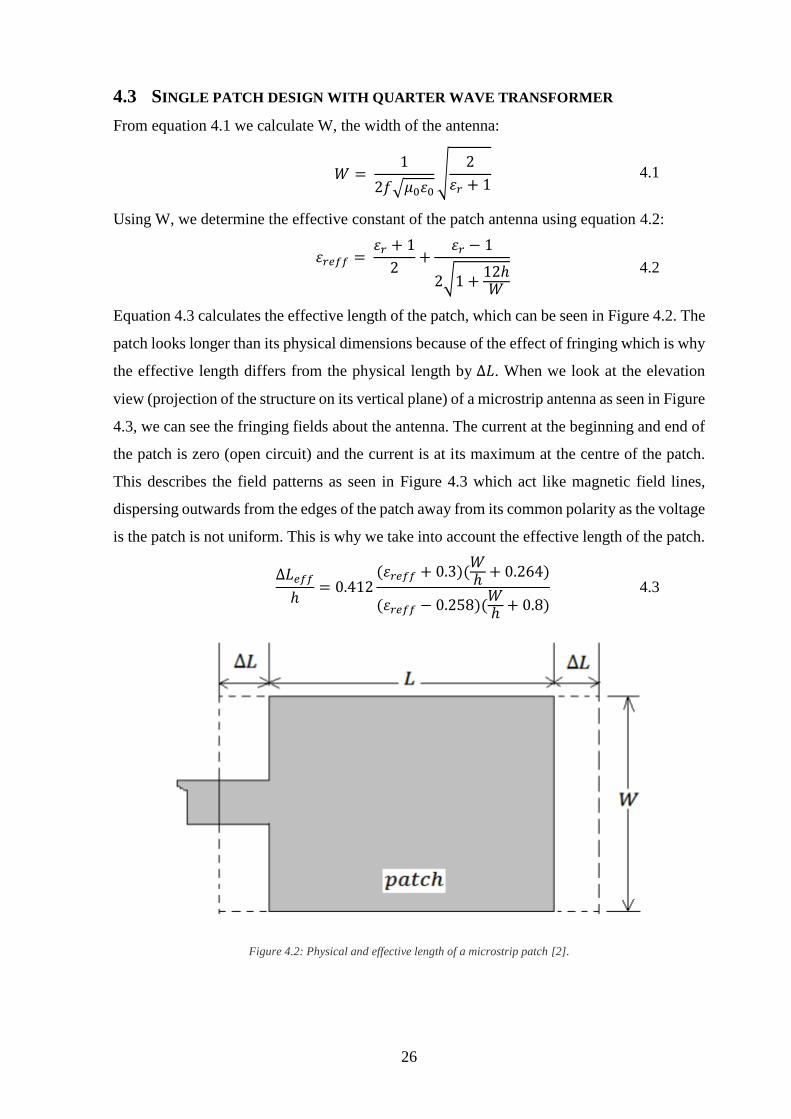
Equation 4.3 calculates the effective length of the patch, which can be seen in Figure 4.2. The
patch looks longer than its physical dimensions because of the effect of fringing which is why
the effective length differs from the physical length by ∆𝐿. When we look at the elevation
view (projection of the structure on its vertical plane) of a microstrip antenna as seen in Figure
4.3, we can see the fringing fields about the antenna. The current at the beginning and end of
the patch is zero (open circuit) and the current is at its maximum at the centre of the patch.
This describes the field patterns as seen in Figure 4.3 which act like magnetic field lines,
dispersing outwards from the edges of the patch away from its common polarity as the voltage
is the patch is not uniform. This is why we take into account the effective length of the patch.
∆𝐿𝑒𝑓𝑓
ℎ= 0.412
(𝜀𝑟𝑒𝑓𝑓 + 0.3)(𝑊ℎ
+ 0.264)
(𝜀𝑟𝑒𝑓𝑓 − 0.258)(𝑊ℎ
+ 0.8) 4.3
Figure 4.2: Physical and effective length of a microstrip patch [2].
27
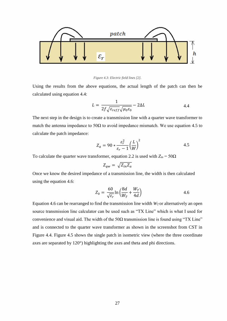
Figure 4.3: Electric field lines [2].
Using the results from the above equations, the actual length of the patch can then be
calculated using equation 4.4:
𝐿 = 1
2𝑓√𝜀𝑟𝑒𝑓𝑓√𝜇0𝜀0
− 2∆𝐿 4.4
The next step in the design is to create a transmission line with a quarter wave transformer to
match the antenna impedance to 50Ω to avoid impedance mismatch. We use equation 4.5 to
calculate the patch impedance:
𝑍𝑎 = 90 ∗𝜀𝑟
2
𝜀𝑟 − 1(
𝐿
𝑊)
2
4.5
To calculate the quarter wave transformer, equation 2.2 is used with Zin = 50Ω
𝑍𝑞𝑤 = √𝑍𝑖𝑛𝑍𝑎
Once we know the desired impedance of a transmission line, the width is then calculated
using the equation 4.6:
𝑍0 = 60
√𝜀𝑟
ln (8𝑑
𝑊𝑇+
𝑊𝑇
4𝑑) 4.6
Equation 4.6 can be rearranged to find the transmission line width WT or alternatively an open
source transmission line calculator can be used such as “TX Line” which is what I used for
convenience and visual aid. The width of the 50Ω transmission line is found using “TX Line”
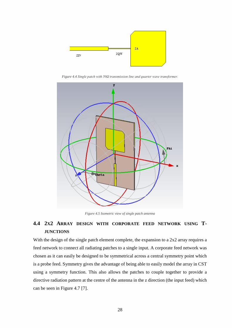
and is connected to the quarter wave transformer as shown in the screenshot from CST in
Figure 4.4. Figure 4.5 shows the single patch in isometric view (where the three coordinate
axes are separated by 120°) highlighting the axes and theta and phi directions.
28
Figure 4.4 Single patch with 50Ω transmission line and quarter wave transformer.
Figure 4.5 Isometric view of single patch antenna
4.4 2X2 ARRAY DESIGN WITH CORPORATE FEED NETWORK USING T-
JUNCTIONS
With the design of the single patch element complete, the expansion to a 2x2 array requires a
feed network to connect all radiating patches to a single input. A corporate feed network was
chosen as it can easily be designed to be symmetrical across a central symmetry point which
is a probe feed. Symmetry gives the advantage of being able to easily model the array in CST
using a symmetry function. This also allows the patches to couple together to provide a
directive radiation pattern at the centre of the antenna in the z direction (the input feed) which
can be seen in Figure 4.7 [7].
29
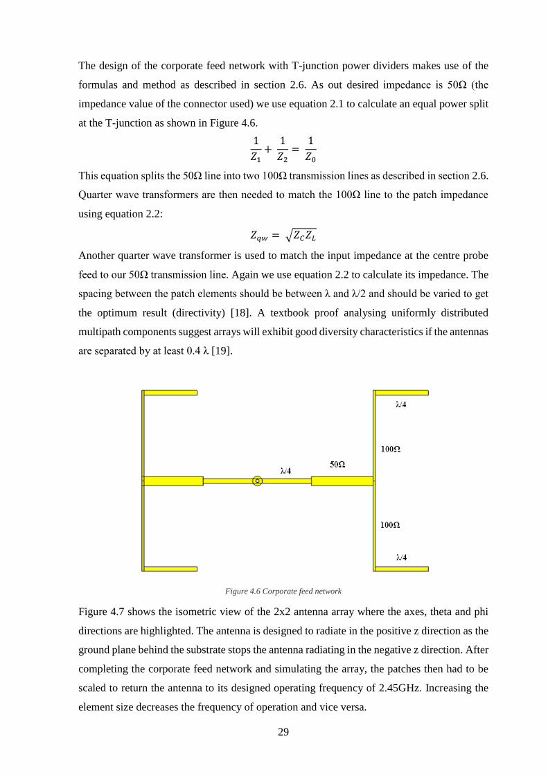
The design of the corporate feed network with T-junction power dividers makes use of the
formulas and method as described in section 2.6. As out desired impedance is 50Ω (the
impedance value of the connector used) we use equation 2.1 to calculate an equal power split
at the T-junction as shown in Figure 4.6.
1
𝑍1+
1
𝑍2=
1
𝑍0
This equation splits the 50Ω line into two 100Ω transmission lines as described in section 2.6.
Quarter wave transformers are then needed to match the 100Ω line to the patch impedance
using equation 2.2:
𝑍𝑞𝑤 = √𝑍𝐶𝑍𝐿
Another quarter wave transformer is used to match the input impedance at the centre probe
feed to our 50Ω transmission line. Again we use equation 2.2 to calculate its impedance. The
spacing between the patch elements should be between λ and λ/2 and should be varied to get
the optimum result (directivity) [18]. A textbook proof analysing uniformly distributed
multipath components suggest arrays will exhibit good diversity characteristics if the antennas
are separated by at least 0.4 λ [19].
Figure 4.6 Corporate feed network
Figure 4.7 shows the isometric view of the 2x2 antenna array where the axes, theta and phi
directions are highlighted. The antenna is designed to radiate in the positive z direction as the
ground plane behind the substrate stops the antenna radiating in the negative z direction. After
completing the corporate feed network and simulating the array, the patches then had to be
scaled to return the antenna to its designed operating frequency of 2.45GHz. Increasing the
element size decreases the frequency of operation and vice versa.
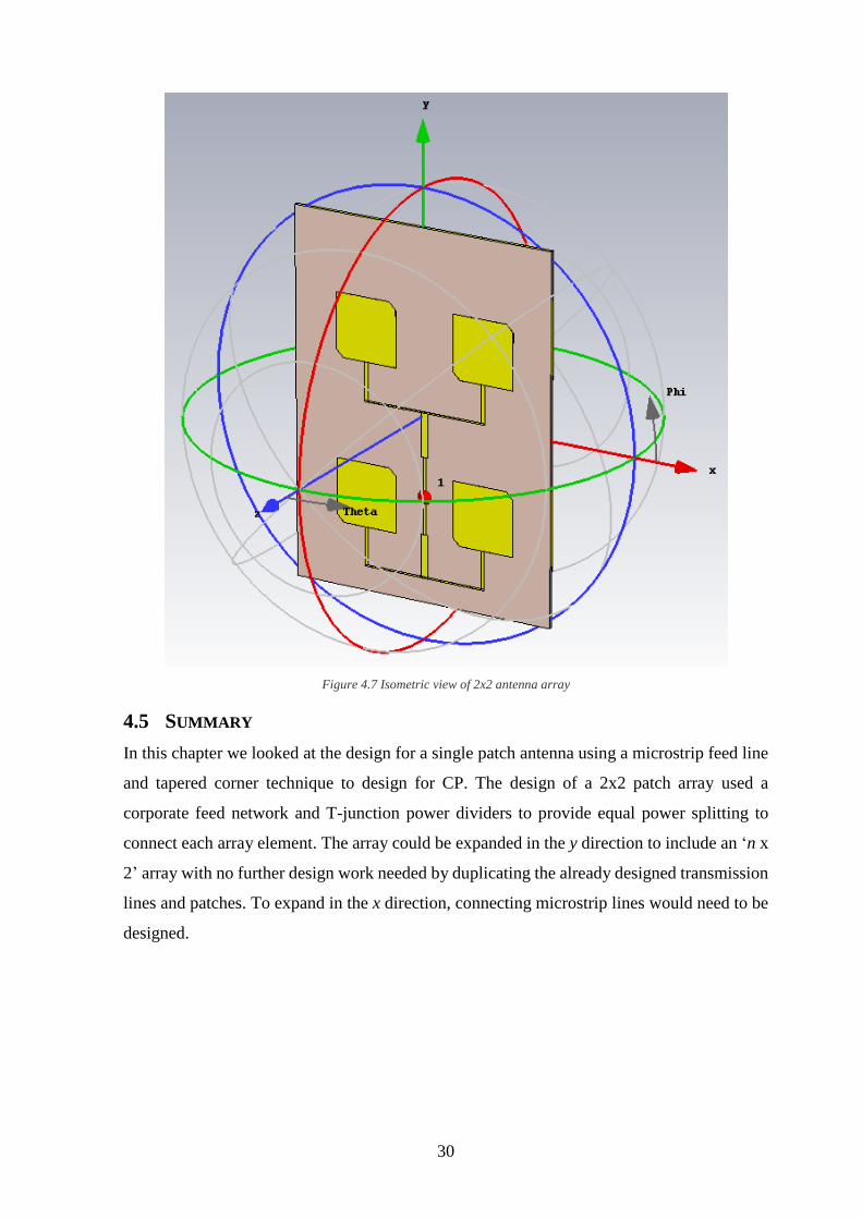
30
Figure 4.7 Isometric view of 2x2 antenna array
4.5 SUMMARY
In this chapter we looked at the design for a single patch antenna using a microstrip feed line
and tapered corner technique to design for CP. The design of a 2x2 patch array used a
corporate feed network and T-junction power dividers to provide equal power splitting to
connect each array element. The array could be expanded in the y direction to include an ‘n x
2’ array with no further design work needed by duplicating the already designed transmission
lines and patches. To expand in the x direction, connecting microstrip lines would need to be
designed.
31
Chapter 5 RESULTS AND DISCUSSION
In this chapter, we look at the simulation results for the single patch and compare the
simulation and measured results for the array of patches. Simulation results nearly always
differ to measured results as simulations are calculated in ideal conditions whereas
measurement are not.
5.1 SINGLE PATCH SIMULATION RESULTS
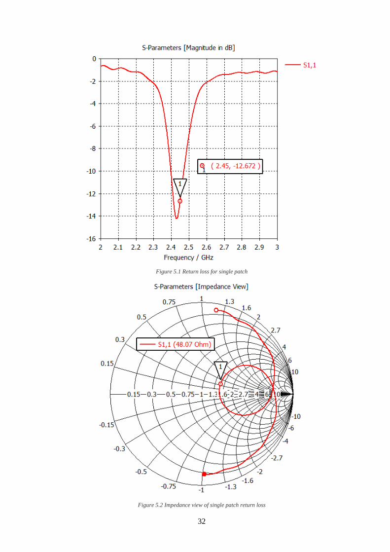
5.1.1 Return loss
Figure 5.1 shows the simulated return loss of the single patch. The resonance is nearly centred
at 2.45GHz with a value of -12.672dB. Using the decibel to linear table in the Appendix or
equation 3.3, a return loss value of -12.672dB reflects back 23% of the input power. As this
is a simulation, this result acceptable. When measuring a physical antenna with a VNA, the
antenna can be tuned to give a better return loss than the simulation so we do not waste time
simulating to get the ‘perfect’ return loss. This resonance can be moved with the scaling of
the patches as mentioned in the previous section. This result shows that the antenna impedance
is matched near our desired impedance of 50Ω as return loss is proportional to impedance
which can be seen from the smith chart in Figure 5.2.
32
Figure 5.1 Return loss for single patch
Figure 5.2 Impedance view of single patch return loss
33
5.1.2 Directivity
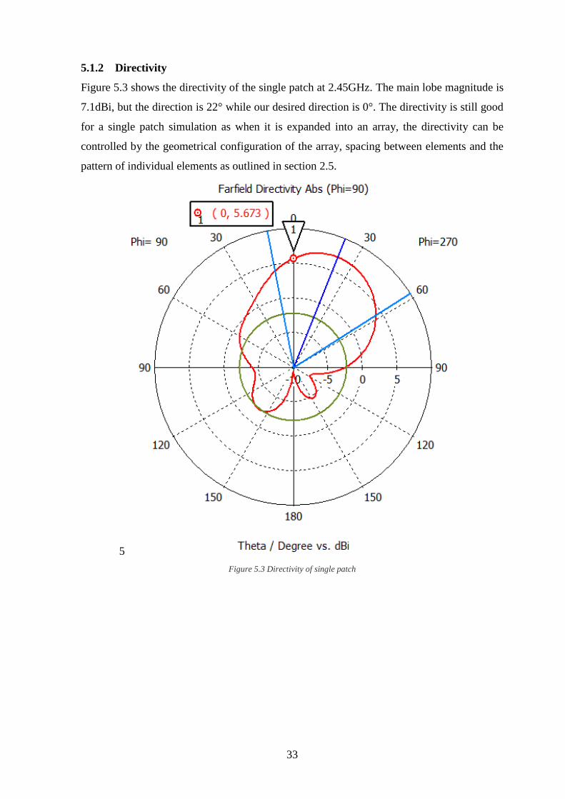
Figure 5.3 shows the directivity of the single patch at 2.45GHz. The main lobe magnitude is
7.1dBi, but the direction is 22° while our desired direction is 0°. The directivity is still good
for a single patch simulation as when it is expanded into an array, the directivity can be
controlled by the geometrical configuration of the array, spacing between elements and the
pattern of individual elements as outlined in section 2.5.
5
Figure 5.3 Directivity of single patch
34
5.1.3 Gain
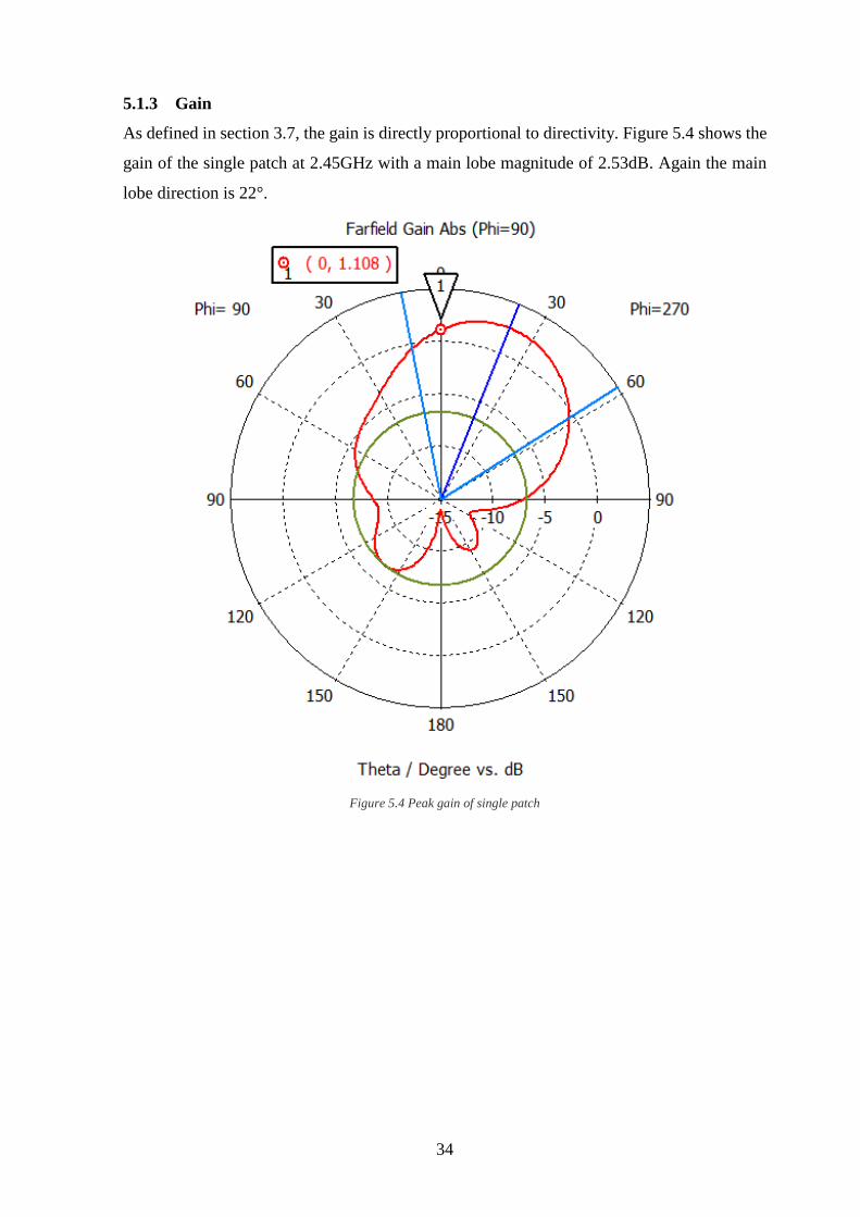
As defined in section 3.7, the gain is directly proportional to directivity. Figure 5.4 shows the
gain of the single patch at 2.45GHz with a main lobe magnitude of 2.53dB. Again the main
lobe direction is 22°.
Figure 5.4 Peak gain of single patch
35
5.1.4 Efficiency
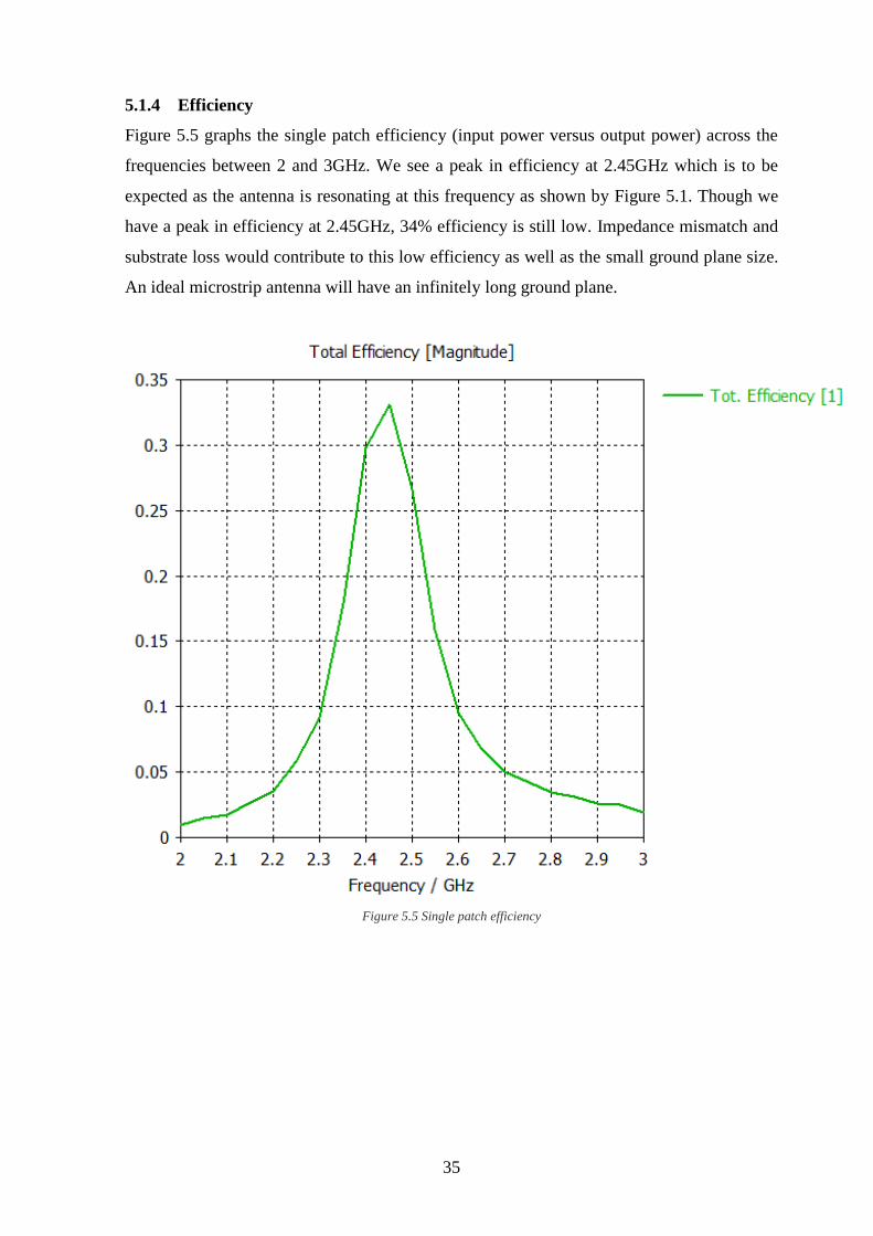
Figure 5.5 graphs the single patch efficiency (input power versus output power) across the
frequencies between 2 and 3GHz. We see a peak in efficiency at 2.45GHz which is to be
expected as the antenna is resonating at this frequency as shown by Figure 5.1. Though we
have a peak in efficiency at 2.45GHz, 34% efficiency is still low. Impedance mismatch and
substrate loss would contribute to this low efficiency as well as the small ground plane size.
An ideal microstrip antenna will have an infinitely long ground plane.
Figure 5.5 Single patch efficiency
36
5.1.5 Axial Ratio
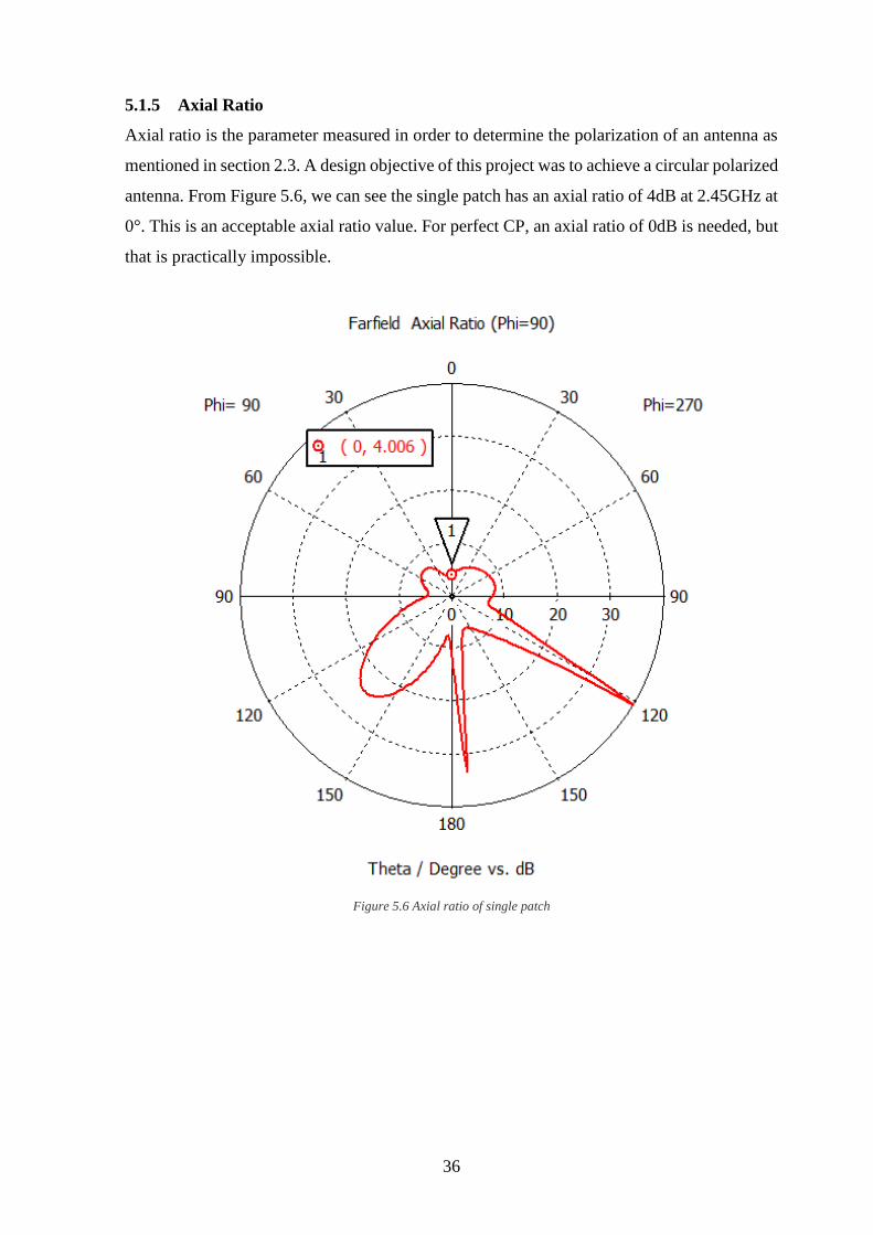
Axial ratio is the parameter measured in order to determine the polarization of an antenna as
mentioned in section 2.3. A design objective of this project was to achieve a circular polarized
antenna. From Figure 5.6, we can see the single patch has an axial ratio of 4dB at 2.45GHz at
0°. This is an acceptable axial ratio value. For perfect CP, an axial ratio of 0dB is needed, but
that is practically impossible.
Figure 5.6 Axial ratio of single patch
37
5.1.6 Radiation pattern
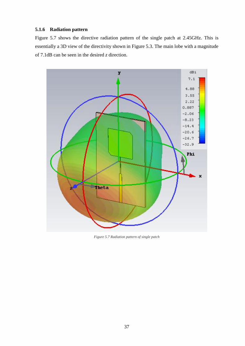
Figure 5.7 shows the directive radiation pattern of the single patch at 2.45GHz. This is
essentially a 3D view of the directivity shown in Figure 5.3. The main lobe with a magnitude
of 7.1dB can be seen in the desired z direction.
Figure 5.7 Radiation pattern of single patch
38
5.2 ANTENNA ARRAY SIMULATION AND MEASURED RESULTS
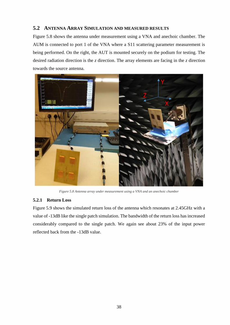
Figure 5.8 shows the antenna under measurement using a VNA and anechoic chamber. The
AUM is connected to port 1 of the VNA where a S11 scattering parameter measurement is
being performed. On the right, the AUT is mounted securely on the podium for testing. The
desired radiation direction is the z direction. The array elements are facing in the z direction
towards the source antenna.
Figure 5.8 Antenna array under measurement using a VNA and an anechoic chamber
5.2.1 Return Loss
Figure 5.9 shows the simulated return loss of the antenna which resonates at 2.45GHz with a
value of -13dB like the single patch simulation. The bandwidth of the return loss has increased
considerably compared to the single patch. We again see about 23% of the input power
reflected back from the -13dB value.
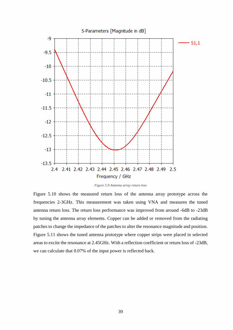
39
Figure 5.9 Antenna array return loss
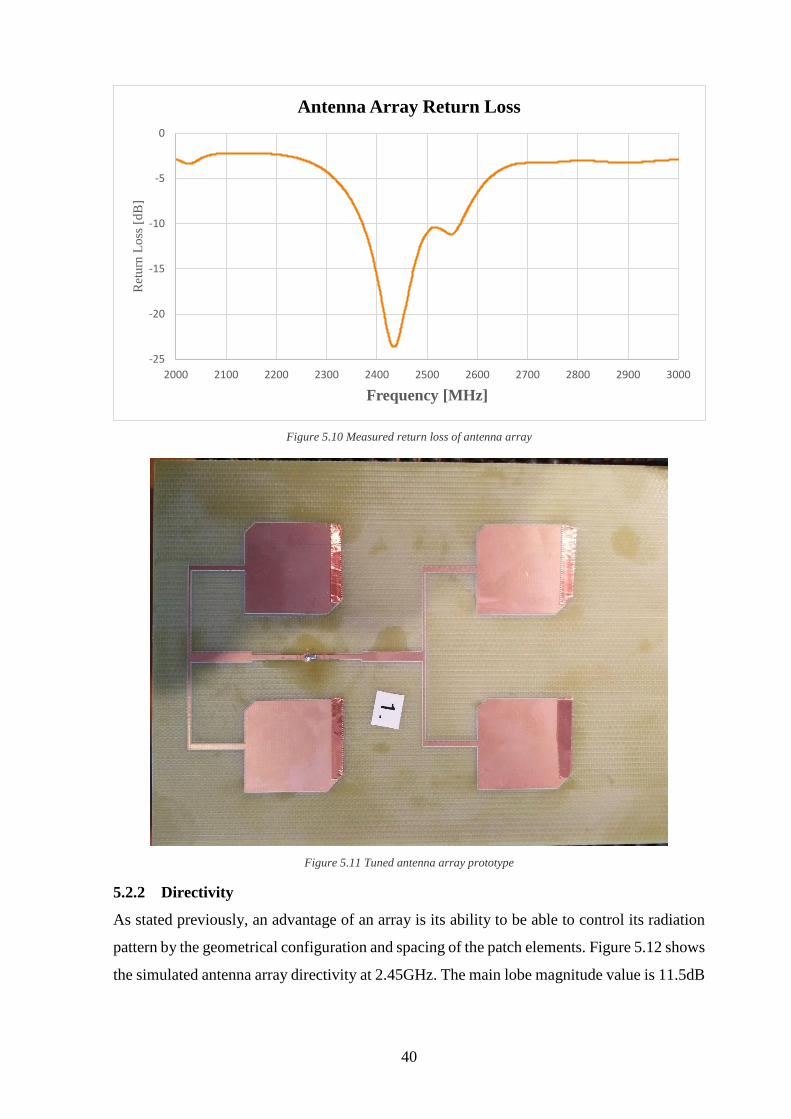
Figure 5.10 shows the measured return loss of the antenna array prototype across the
frequencies 2-3GHz. This measurement was taken using VNA and measures the tuned
antenna return loss. The return loss performance was improved from around -6dB to -23dB
by tuning the antenna array elements. Copper can be added or removed from the radiating
patches to change the impedance of the patches to alter the resonance magnitude and position.
Figure 5.11 shows the tuned antenna prototype where copper strips were placed in selected
areas to excite the resonance at 2.45GHz. With a reflection coefficient or return loss of -23dB,
we can calculate that 0.07% of the input power is reflected back.
40
Figure 5.10 Measured return loss of antenna array
Figure 5.11 Tuned antenna array prototype
5.2.2 Directivity
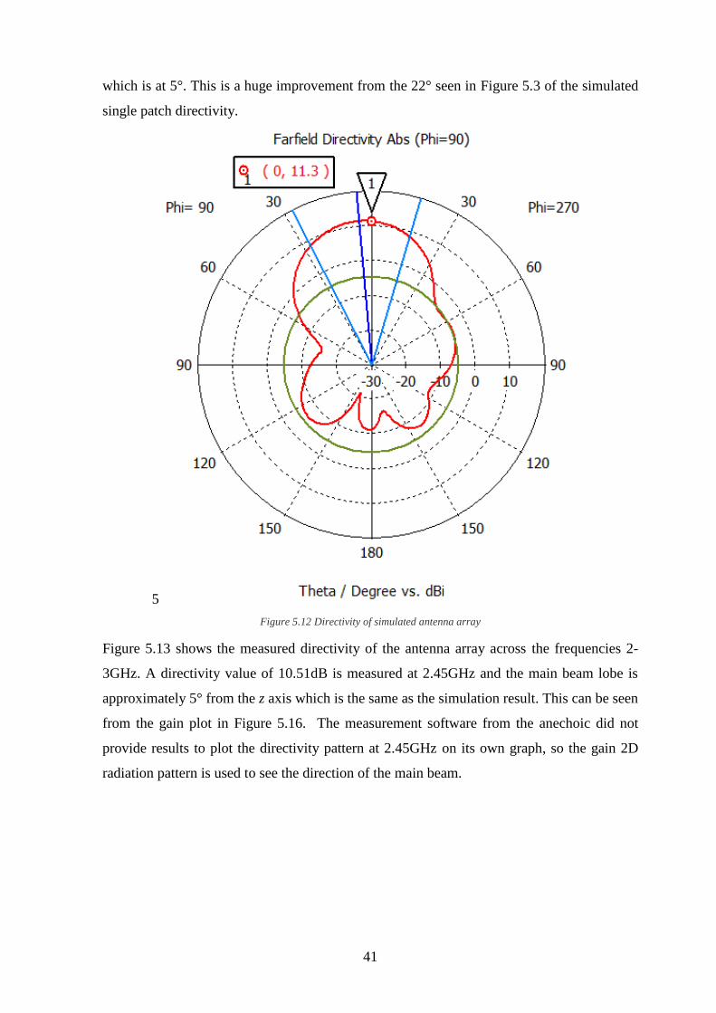
As stated previously, an advantage of an array is its ability to be able to control its radiation
pattern by the geometrical configuration and spacing of the patch elements. Figure 5.12 shows
the simulated antenna array directivity at 2.45GHz. The main lobe magnitude value is 11.5dB
-25
-20
-15
-10
-5
0
2000 2100 2200 2300 2400 2500 2600 2700 2800 2900 3000
Ret
urn
Lo
ss [
dB
]
Frequency [MHz]
Antenna Array Return Loss
41
which is at 5°. This is a huge improvement from the 22° seen in Figure 5.3 of the simulated
single patch directivity.
5
Figure 5.12 Directivity of simulated antenna array
Figure 5.13 shows the measured directivity of the antenna array across the frequencies 2-
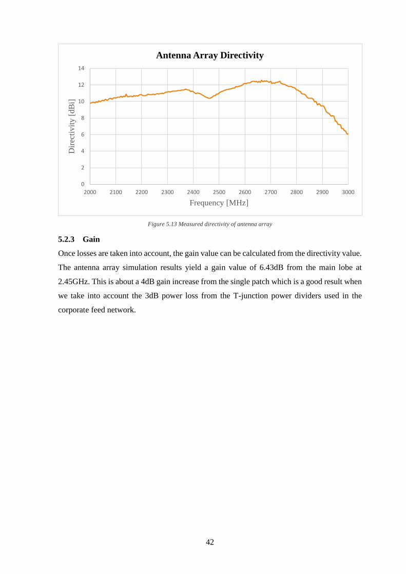
3GHz. A directivity value of 10.51dB is measured at 2.45GHz and the main beam lobe is
approximately 5° from the z axis which is the same as the simulation result. This can be seen
from the gain plot in Figure 5.16. The measurement software from the anechoic did not
provide results to plot the directivity pattern at 2.45GHz on its own graph, so the gain 2D
radiation pattern is used to see the direction of the main beam.
42
Figure 5.13 Measured directivity of antenna array
5.2.3 Gain
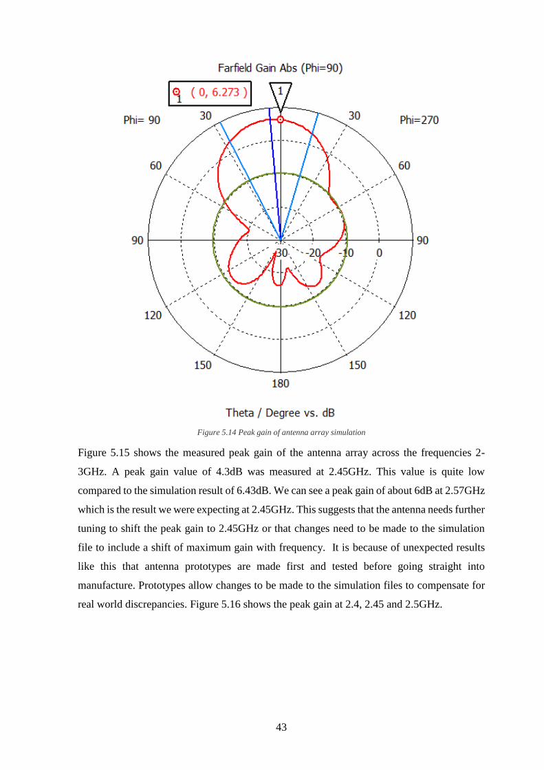
Once losses are taken into account, the gain value can be calculated from the directivity value.
The antenna array simulation results yield a gain value of 6.43dB from the main lobe at
2.45GHz. This is about a 4dB gain increase from the single patch which is a good result when
we take into account the 3dB power loss from the T-junction power dividers used in the
corporate feed network.
0
2
4
6
8
10
12
14
2000 2100 2200 2300 2400 2500 2600 2700 2800 2900 3000
Dir
ecti
vit
y [
dB
i]
Frequency [MHz]
Antenna Array Directivity
43
Figure 5.14 Peak gain of antenna array simulation
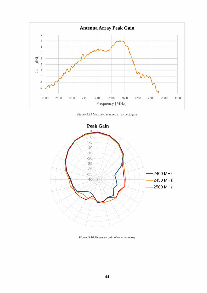
Figure 5.15 shows the measured peak gain of the antenna array across the frequencies 2-
3GHz. A peak gain value of 4.3dB was measured at 2.45GHz. This value is quite low
compared to the simulation result of 6.43dB. We can see a peak gain of about 6dB at 2.57GHz
which is the result we were expecting at 2.45GHz. This suggests that the antenna needs further
tuning to shift the peak gain to 2.45GHz or that changes need to be made to the simulation
file to include a shift of maximum gain with frequency. It is because of unexpected results
like this that antenna prototypes are made first and tested before going straight into
manufacture. Prototypes allow changes to be made to the simulation files to compensate for
real world discrepancies. Figure 5.16 shows the peak gain at 2.4, 2.45 and 2.5GHz.
44
Figure 5.15 Measured antenna array peak gain
Figure 5.16 Measured gain of antenna array
-3
-2
-1
0
1
2
3
4
5
6
7
2000 2100 2200 2300 2400 2500 2600 2700 2800 2900 3000
Gai
n [
dB
i]
Frequency [MHz]
Antenna Array Peak Gain
-40
-35
-30
-25
-20
-15
-10
-5
0
5
Peak Gain
2400 MHz
2450 MHz
2500 MHz
45
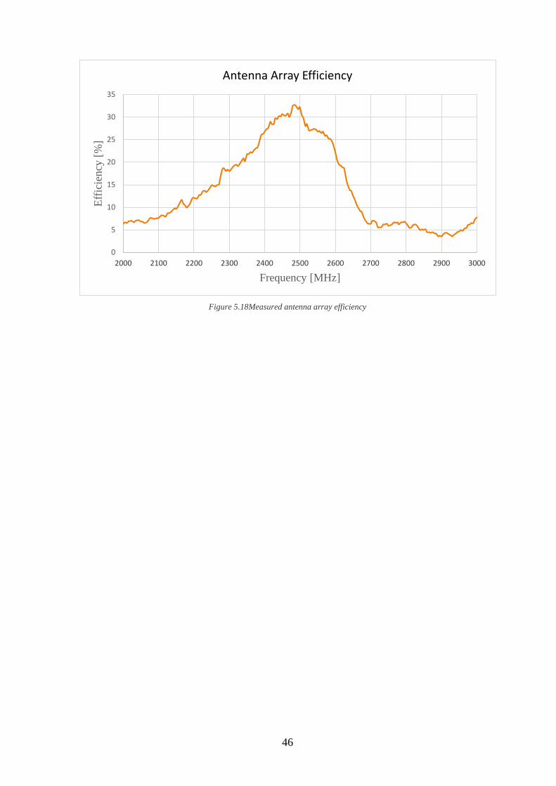
5.2.4 Efficiency
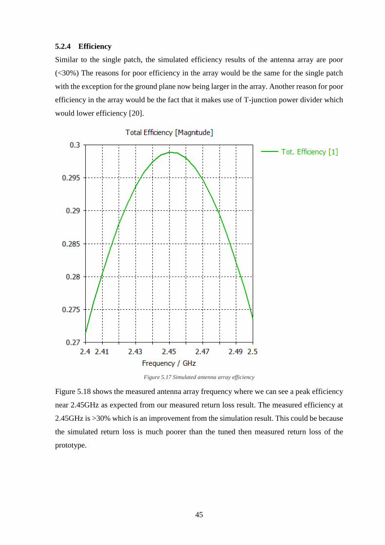
Similar to the single patch, the simulated efficiency results of the antenna array are poor
(<30%) The reasons for poor efficiency in the array would be the same for the single patch
with the exception for the ground plane now being larger in the array. Another reason for poor
efficiency in the array would be the fact that it makes use of T-junction power divider which
would lower efficiency [20].
Figure 5.17 Simulated antenna array efficiency
Figure 5.18 shows the measured antenna array frequency where we can see a peak efficiency
near 2.45GHz as expected from our measured return loss result. The measured efficiency at
2.45GHz is >30% which is an improvement from the simulation result. This could be because
the simulated return loss is much poorer than the tuned then measured return loss of the
prototype.
46
Figure 5.18Measured antenna array efficiency
0
5
10
15
20
25
30
35
2000 2100 2200 2300 2400 2500 2600 2700 2800 2900 3000
Eff
icie
ncy
[%
]
Frequency [MHz]
Antenna Array Efficiency
47
5.2.5 Axial Ratio
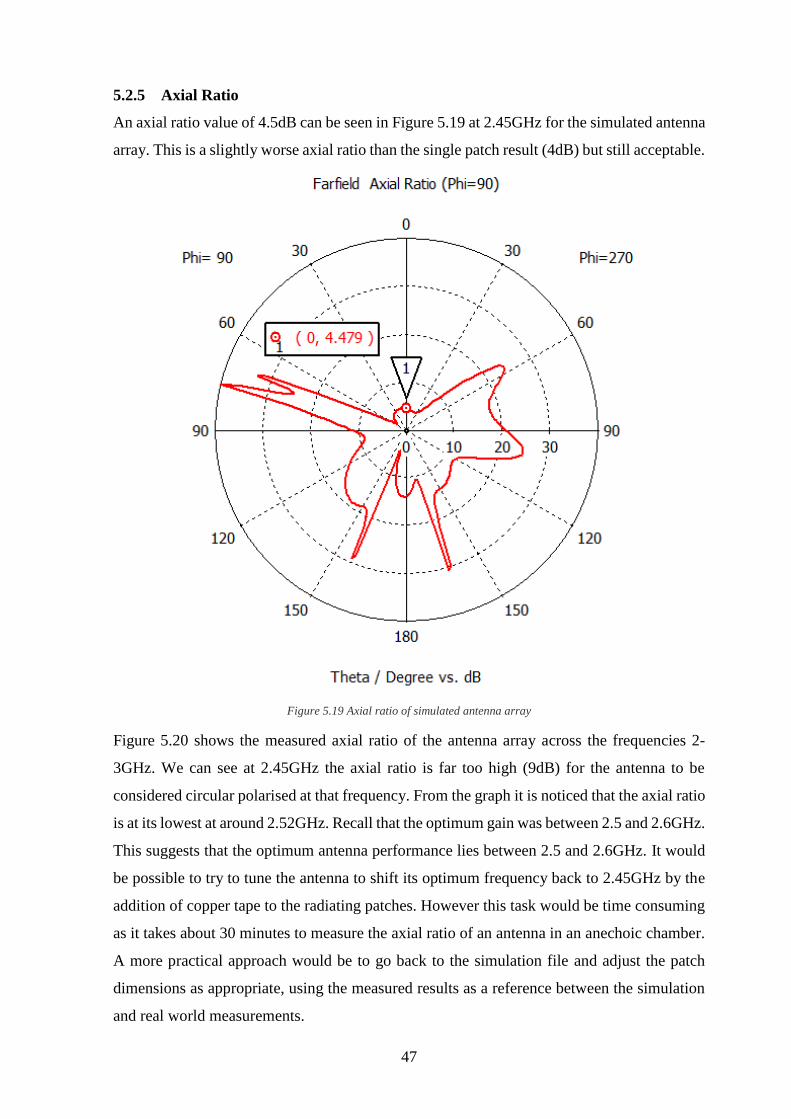
An axial ratio value of 4.5dB can be seen in Figure 5.19 at 2.45GHz for the simulated antenna
array. This is a slightly worse axial ratio than the single patch result (4dB) but still acceptable.
Figure 5.19 Axial ratio of simulated antenna array
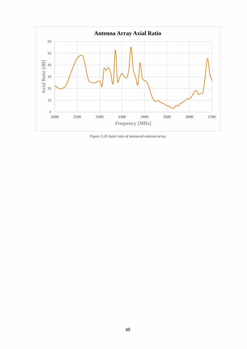
Figure 5.20 shows the measured axial ratio of the antenna array across the frequencies 2-
3GHz. We can see at 2.45GHz the axial ratio is far too high (9dB) for the antenna to be
considered circular polarised at that frequency. From the graph it is noticed that the axial ratio
is at its lowest at around 2.52GHz. Recall that the optimum gain was between 2.5 and 2.6GHz.
This suggests that the optimum antenna performance lies between 2.5 and 2.6GHz. It would
be possible to try to tune the antenna to shift its optimum frequency back to 2.45GHz by the
addition of copper tape to the radiating patches. However this task would be time consuming
as it takes about 30 minutes to measure the axial ratio of an antenna in an anechoic chamber.
A more practical approach would be to go back to the simulation file and adjust the patch
dimensions as appropriate, using the measured results as a reference between the simulation
and real world measurements.
48
Figure 5.20 Axial ratio of measured antenna array
0
10
20
30
40
50
60
2000 2100 2200 2300 2400 2500 2600 2700
Ax
ial
Rat
io [
dB
]
Frequency [MHz]
Antenna Array Axial Ratio
49
5.2.6 Radiation Pattern
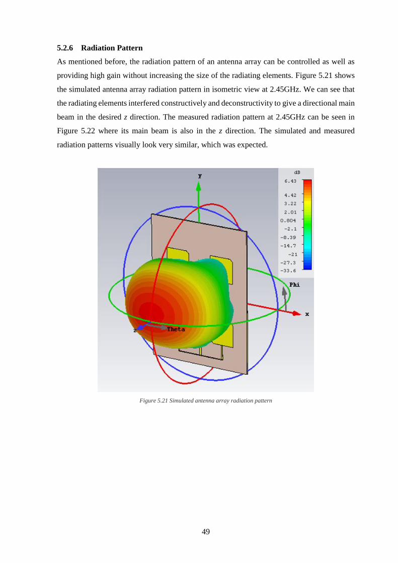
As mentioned before, the radiation pattern of an antenna array can be controlled as well as
providing high gain without increasing the size of the radiating elements. Figure 5.21 shows
the simulated antenna array radiation pattern in isometric view at 2.45GHz. We can see that
the radiating elements interfered constructively and deconstructivity to give a directional main
beam in the desired z direction. The measured radiation pattern at 2.45GHz can be seen in
Figure 5.22 where its main beam is also in the z direction. The simulated and measured
radiation patterns visually look very similar, which was expected.
Figure 5.21 Simulated antenna array radiation pattern
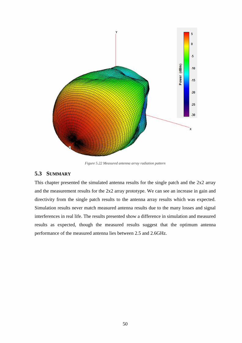
50
Figure 5.22 Measured antenna array radiation pattern
5.3 SUMMARY
This chapter presented the simulated antenna results for the single patch and the 2x2 array
and the measurement results for the 2x2 array prototype. We can see an increase in gain and
directivity from the single patch results to the antenna array results which was expected.
Simulation results never match measured antenna results due to the many losses and signal
interferences in real life. The results presented show a difference in simulation and measured
results as expected, though the measured results suggest that the optimum antenna
performance of the measured antenna lies between 2.5 and 2.6GHz.

51
Chapter 6 ETHICS
This chapter discusses the ethical issues encountered throughout this project. The fact this is
a university based project where a company is also involved brings certain ethical issues to
light. Though DCU coordinated this project, an external company agreed to allow the use of
their measurement, mechanical and electronic equipment as well as the licence for the design
software CST.
6.1 THE LEGAL AND ETHICAL USE OF SOFTWARE
The software used in this project was Matlab, CST and TX line. Unauthorized copying of
software is illegal. If unauthorized copying proliferated on DCU campus, the university may
incur legal liability also. An individual can harm the entire academic community with the use
of unlicensed software as an institution may find it more difficult to negotiate agreements to
make software less expensively available to members of the academic community [21].
Matlab and CST are classified as commercial software, with DCU supplying a student licence
for Matlab and the external company supplying the commercial licence for CST. It is
important to know that once a licence for a particular software package is acquired, the
company who produced the software still owns the copyright. Use of the software is under
the terms and conditions of the licence agreement. This agreement may include restrictions
such as the copying of the software if the original package fails, modifications of the software,
decompiling the program code and development of new works built upon the package [21].
TX line is an open source software package where it can be freely downloaded legally once
you register online. This would be classified as “Freeware” which is also covered by copyright
and subject to terms and conditions.
6.2 CONFIDENTIALITY WITH AN EXTERNAL COMPANY
The ethical issue of confidentially can be described as “the limiting of access to information
to those who have either a legal or an ethical right to that access [22]”. Working with an
external company while doing this project often exposed me to commercially sensitive
information about the company. This information could include ongoing projects in the
company, patent pending antennas or patents held by the company. The exact design of an
antenna is not often disclosed to customers or the public. The dielectric constant of a substrate
or the exact design of the metallic trace of an antenna would be kept confidential. While

52
working with an external company, it is important to be aware of any confidentially
requirements attached to data to which you have access.
A case could arise where a bribe was offered in exchange for confidential information about
the company. It is the duty of the engineer to “reject bribery or improper influence [23]” when
cases such as these arise and to “not without proper authority disclose any confidential
information concerning the business of their employer or any past employer. [22]”This still
begs the question of what constitutes proper authority and what counts as confidential
information? In questionable cases, individual judgement should be exercised though making
sure to be aware of all relevant legal and contractual requirements [22].
6.3 HEALTH AND SAFETY
For the most part of this project there were little or no health and safety risks as the antenna
was designed using software packages. Once the antenna was fabricated, the proper testing
procedures had to be carried out while following the associated health and safety procedures.
The health and safety document provided by the external company was read and expected to
have been read prior to the use of any equipment. The proper health and safety apparel was
also expected and to “always act with care and competence [23]”
A drill and soldering iron was used to connect the probe feed connector to the antenna before
testing. Safety goggles were worn when drilling and loose clothing was tied back. An
extractor fan was used to extract toxic fumes while soldering as well as adequate lighting.
Protective gloves were worn while handling the absorber wedges in the anechoic chamber
which contain nickel-ferrite and should not be consumed accidently.
6.4 TESTING
Testing is an essential procedure to validate antenna performance. It is important to provide
sufficient testing so as to provide accurate reliable results for documentation which will be
associated with the device under measurement. The procedures followed when carrying out
the testing of the antenna should adhere to the ‘rule’ from the Institution of Engineering
Technology: “Members shall at all times take all reasonable care to limit any danger of death,
injury or ill health to any person that may result from their work and the products of their
work. [22]”
An antenna once designed can be integrated into a number of different devices from different
industry sectors such as agriculture and medical. The antenna in question could be used in a

53
medical device to monitor a patient or could be used in an agricultural vehicle for steering
using GPS. It is therefore important to provide accurate and a sufficient quantity of test results
to compile an accurate specification sheet for that antenna, outlining the antennas’ capabilities
and tolerances.
6.5 CONCLUSION
This chapter has raised and discussed the ethical issues associated with this project. It is
important to adhere to ethical ‘rules’ in all aspects of engineering including academic and
industry based projects. Engineering ethics reflects the customs, values and traditions of
engineering as a profession and it is needed to answer ethical questions posed to engineers by
the public, governments and the media.
54
Chapter 7 CONCLUSIONS
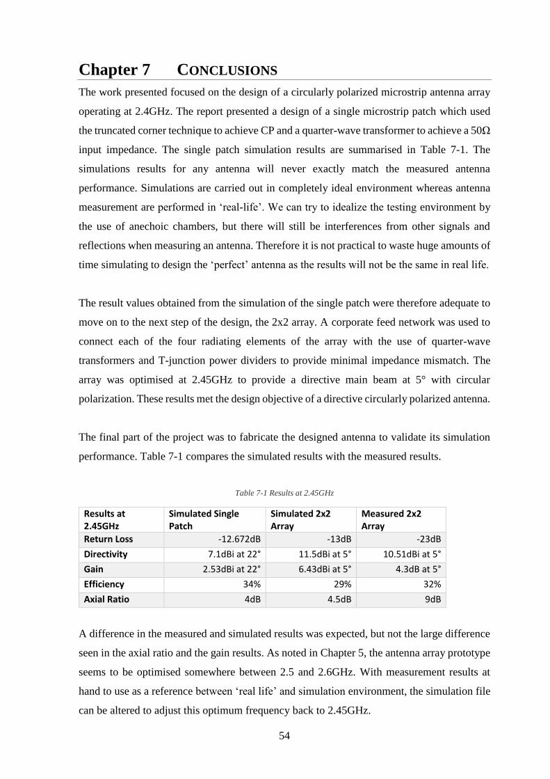
The work presented focused on the design of a circularly polarized microstrip antenna array
operating at 2.4GHz. The report presented a design of a single microstrip patch which used
the truncated corner technique to achieve CP and a quarter-wave transformer to achieve a 50Ω
input impedance. The single patch simulation results are summarised in Table 7-1. The
simulations results for any antenna will never exactly match the measured antenna
performance. Simulations are carried out in completely ideal environment whereas antenna
measurement are performed in ‘real-life’. We can try to idealize the testing environment by
the use of anechoic chambers, but there will still be interferences from other signals and
reflections when measuring an antenna. Therefore it is not practical to waste huge amounts of
time simulating to design the ‘perfect’ antenna as the results will not be the same in real life.
The result values obtained from the simulation of the single patch were therefore adequate to
move on to the next step of the design, the 2x2 array. A corporate feed network was used to
connect each of the four radiating elements of the array with the use of quarter-wave
transformers and T-junction power dividers to provide minimal impedance mismatch. The
array was optimised at 2.45GHz to provide a directive main beam at 5° with circular
polarization. These results met the design objective of a directive circularly polarized antenna.
The final part of the project was to fabricate the designed antenna to validate its simulation
performance. Table 7-1 compares the simulated results with the measured results.
Table 7-1 Results at 2.45GHz
Results at 2.45GHz
Simulated Single Patch
Simulated 2x2 Array
Measured 2x2 Array
Return Loss -12.672dB -13dB -23dB
Directivity 7.1dBi at 22° 11.5dBi at 5° 10.51dBi at 5°
Gain 2.53dBi at 22° 6.43dBi at 5° 4.3dB at 5°
Efficiency 34% 29% 32%
Axial Ratio 4dB 4.5dB 9dB
A difference in the measured and simulated results was expected, but not the large difference
seen in the axial ratio and the gain results. As noted in Chapter 5, the antenna array prototype
seems to be optimised somewhere between 2.5 and 2.6GHz. With measurement results at
hand to use as a reference between ‘real life’ and simulation environment, the simulation file
can be altered to adjust this optimum frequency back to 2.45GHz.

55
Section 6.4 mentions the possible uses of antennas in medical devices where antenna
performance must be tested before being integrated in such applications. The results presents
shows the importance of testing an antenna before it is put out to manufacture as an antenna
will not give the same performance in real life as the simulation results indicate.

56
REFERENCES
[1] I.-S. S. Board, “IEEE Standard for Definitions of Terms,” IEEE, New York, 2013.
[2] A. F. Alsager, “Design and Analysis of Microstrip Patch Antenna Arrays,” Boras, 2011.
[3] J.-G. Jeong, K. YoungSub and Y. J. Young, “Polarization tunable microstrip patch
antenna for polarization loss compensation,” Antennas and Propagation (ISAP), pp.
321-322, 2014.
[4] M. Shakeeb, “Circularly Polarized Microstrip Antenna,” Quebec, 2010.
[5] A. Z. Narbudowicz, “Advanced Circularly Polarized Microstrip Antennas,” DIT,
Dublin, 2013.
[6] M. A. Yepes, “MULTILAYER ANTENNA ARRAYS FOR ENVIRONMENTAL
SENSING APPLICATIONS,” Georgia, 2010.
[7] G. Kumar and K. P. Ray, Broadband Microstrip Antennas, Boston,London: Artech
House, 2003.
[8] Amritesh and S. . M. Kshetrimayum, “DESIGN OF SQUARE PATCH MICROSTRIP
ANTENNA FOR CIRCULAR POLARIZATION USING IE3D SOFTWARE,”
ORISSA.
[9] R. Garg, P. Bhartia, I. Bahl and A. Ittipiboon, Microstrip Antenna Design Handbook,
London: Artech House, 2001.
[10] C. A. Balanis, Antenna Theory Analysis and Design, New York: John Wiley & Sons,
1997.
[11] Y. Huang and K. Boyle, Antennas From Theory to Practice, John Wiley & Sons, 2008.
[12] K. Y. Yazdandoost and K. Hamaguchi, “Antenna polarization mismatch in body area
network communications,” Antennas and Propagation (EuCAP), pp. 1-4, 2010.
[13] R. M. Faragher, “Effects of Multipath Interference,” Churchill College, University of
Cambridge, 2007.
[14] “www.physics.tutorcircle.com,” [Online]. Available:
http://physics.tutorcircle.com/waves/sound-waves.html. [Accessed 25 March 2016].
[15] J. D. Kraus, Antennas, McGraw Hill, 1988.

57
[16] “Globalspec,” [Online]. Available:
http://www.globalspec.com/reference/59928/203279/9-4-transmission-line-
termination. [Accessed 22nd March 2016].
[17] “Digikey,” [Online]. Available: http://www.digikey.com/-
/media/Images/Article%20Library/TechZone%20Articles/2014/March/The%20Smith
%20Chart%20A%20Graphical%20Tool%20Still%20Vital%20in%20RF%20Design/a
rticle-2014march-the-smith-chart-an-ancient-fig1.jpg?la=en-US&ts=4fe34ed7-7d03-
4a50-b686-. [Accessed 22 March 2016].
[18] M. K. J. G. Satya Prakash Sinha, “Design Of 2x2 Shaped Rectangular Micro strip Array
Antenna For GSM Application,” International Journal of Scientific & Engineering
Research, vol. 6, no. 5, pp. 752-755, 2015.
[19] P. J. Bevelacqua, “ANTENNA ARRAYS: PERFORMANCE LIMITS AND
GEOMETRY,” ARIZONA STATE UNIVERSITY , ARIZONA, 2008.
[20] M. S. Barbetty, “DESIGN AND IMPLEMENTATION OF A TRANSCEIVER AND
A MICROSTRIP CORPORATE FEED FOR SOLID STATE X-BAND RADAR,”
University of Puerto Rico, Puerto Rico, 2005.
[21] EDICOM and ITAA, “Washington University in St. Louis,” January 1993. [Online].
Available: https://wustl.edu/about/compliance-policies/computers-internet-
policies/legal-ethical-software-use/. [Accessed 07 April 2016].
[22] IET, “The Insitution of Engineering and Technology,” IET, 2016. [Online]. Available:
http://www.theiet.org/membership/career/ethics. [Accessed 07 April 2016].
[23] T. R. A. o. Engineering, “The Royal Academy of Engineering,” August 2011. [Online].
Available: http://www.raeng.org.uk/publications/other/engineering-ethics-in-practice-
full. [Accessed 07 April 2016].
[24] J. L. Volakis, Antenna Engineering Handbook, 4th Edition, McGraw-Hill, 2007.
[25] K. K. Singh and S. C. Gupta, “Review and Analysis of Microstrip Patch Array Antenna
with different configurations,” International Journal of Scientific & Engineering
Research, vol. 4, no. 2, pp. 1-6, 2013.
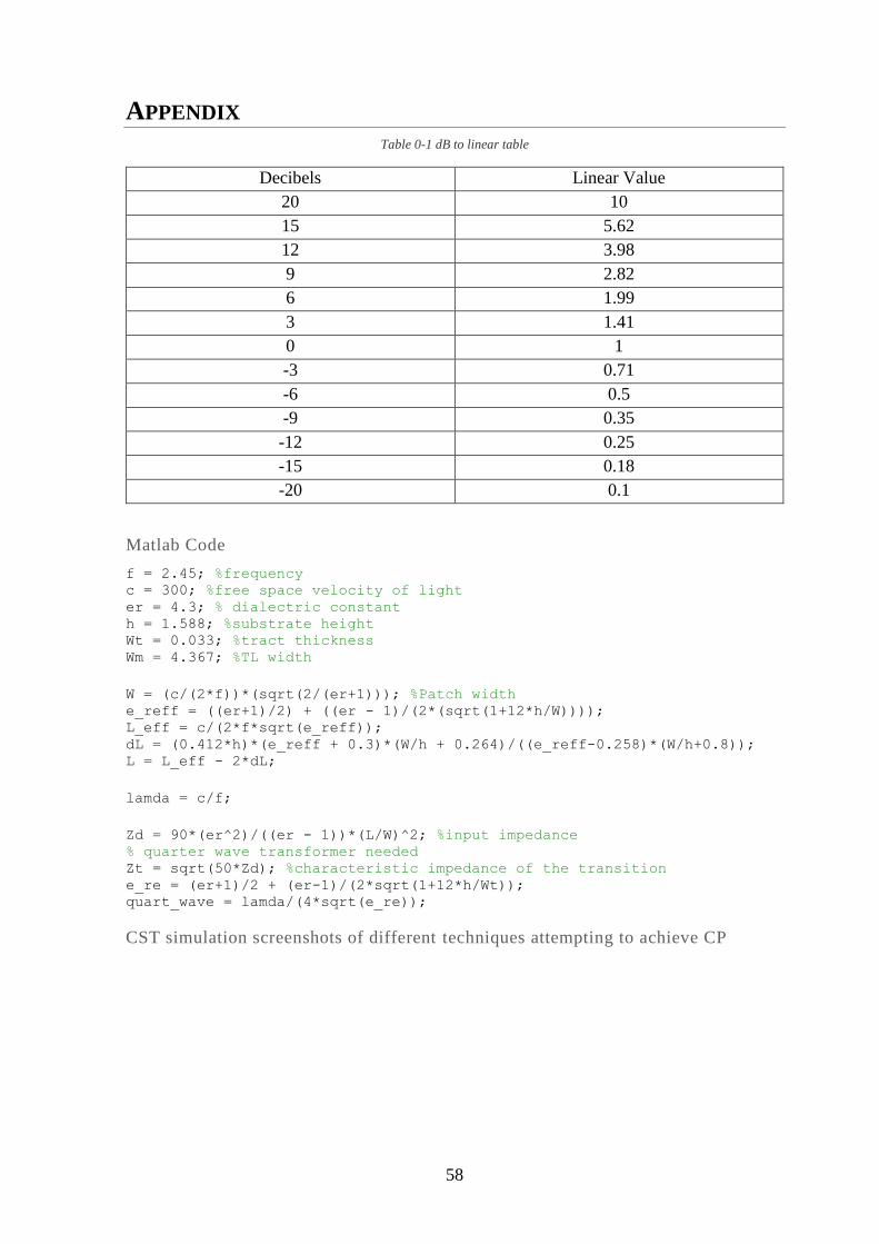
58
APPENDIX Table 0-1 dB to linear table
Decibels Linear Value
20 10
15 5.62
12 3.98
9 2.82
6 1.99
3 1.41
0 1
-3 0.71
-6 0.5
-9 0.35
-12 0.25
-15 0.18
-20 0.1
Matlab Code
f = 2.45; %frequency c = 300; %free space velocity of light er = 4.3; % dialectric constant h = 1.588; %substrate height Wt = 0.033; %tract thickness Wm = 4.367; %TL width
W = (c/(2*f))*(sqrt(2/(er+1))); %Patch width e_reff = ((er+1)/2) + ((er - 1)/(2*(sqrt(1+12*h/W)))); L_eff = c/(2*f*sqrt(e_reff)); dL = (0.412*h)*(e_reff + 0.3)*(W/h + 0.264)/((e_reff-0.258)*(W/h+0.8)); L = L_eff - 2*dL;
lamda = c/f;
Zd = 90*(er^2)/((er - 1))*(L/W)^2; %input impedance % quarter wave transformer needed Zt = sqrt(50*Zd); %characteristic impedance of the transition e_re = (er+1)/2 + (er-1)/(2*sqrt(1+12*h/Wt)); quart_wave = lamda/(4*sqrt(e_re));
CST simulation screenshots of different techniques attempting to achieve CP
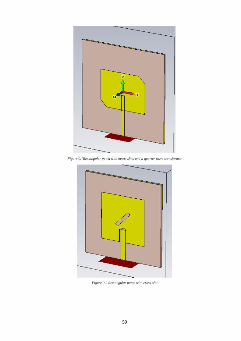
59
Figure 0.1Recatngular patch with insert slots and a quarter wave transformer
Figure 0.2 Rectangular patch with cross-slot
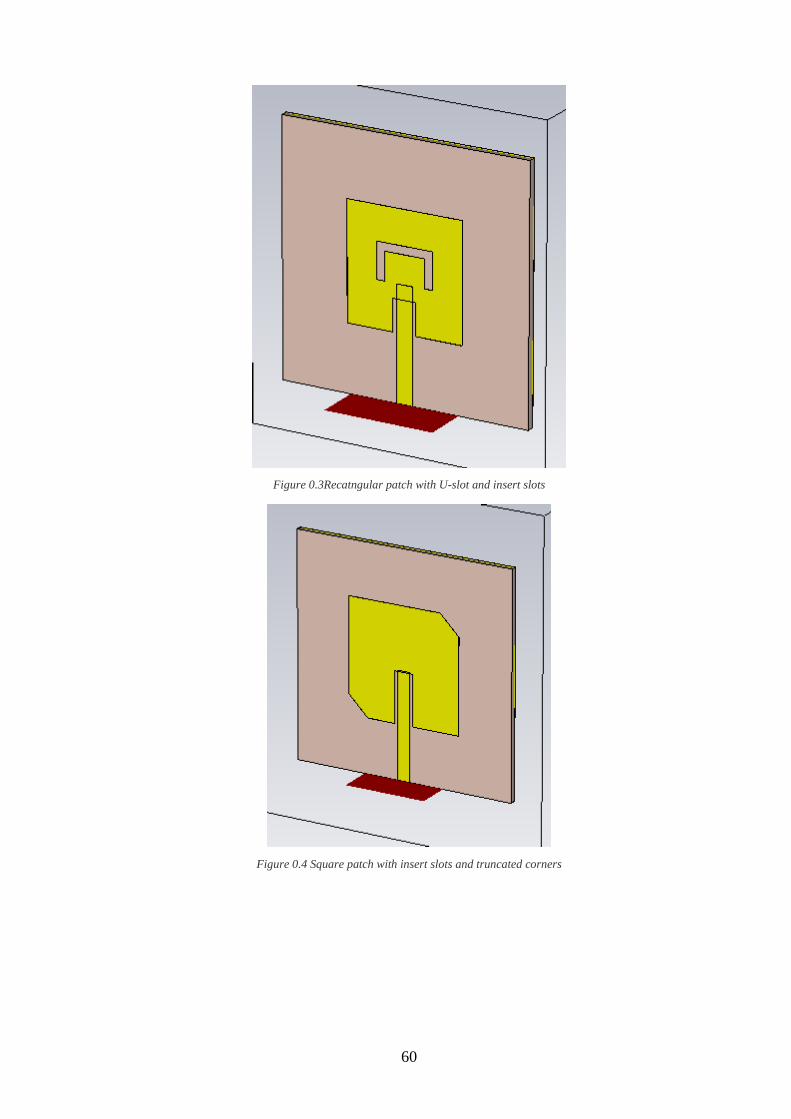
60
Figure 0.3Recatngular patch with U-slot and insert slots
Figure 0.4 Square patch with insert slots and truncated corners


![Design and Performance Analysis of Wide Band Circularly ... · microstrip-patch antenna by using a tuning stub [5]. However, ... “Design of Wideband Circularly Polarized Aperture-Coupled](https://img.pdfslide.us/doc/110x75/5b91ea7e09d3f211298cc768/design-and-performance-analysis-of-wide-band-circularly-microstrip-patch.jpg)