Embed Size (px)
Citation preview
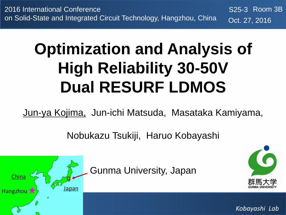
Optimization and Analysis of
High Reliability 30-50V
Dual RESURF LDMOS
Kobayashi Lab
Gunma University, Japan
Jun-ya Kojima, Jun-ichi Matsuda, Masataka Kamiyama,
Nobukazu Tsukiji, Haruo Kobayashi
2016 International Conference
on Solid-State and Integrated Circuit Technology, Hangzhou, China Oct. 27, 2016
S25-3 Room 3B
2/17
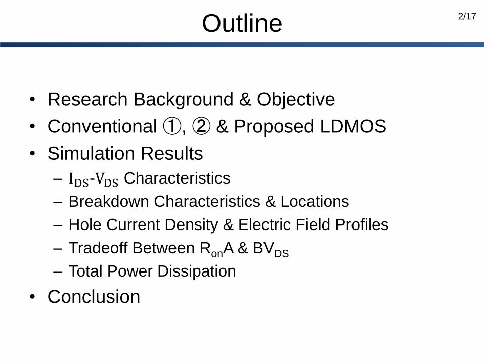
Outline
• Research Background & Objective
• Conventional ①, ② & Proposed LDMOS
• Simulation Results
– IDS-VDS Characteristics
– Breakdown Characteristics & Locations
– Hole Current Density & Electric Field Profiles
– Tradeoff Between RonA & BVDS
– Total Power Dissipation
• Conclusion
3/17
Outline
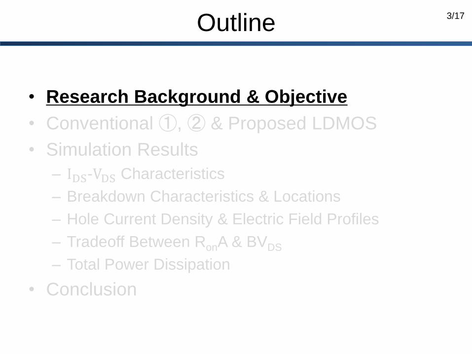
• Research Background & Objective
• Conventional ①, ② & Proposed LDMOS
• Simulation Results
– IDS-VDS Characteristics
– Breakdown Characteristics & Locations
– Hole Current Density & Electric Field Profiles
– Tradeoff Between RonA & BVDS
– Total Power Dissipation
• Conclusion
4/17
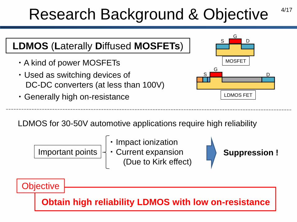
Research Background & Objective
LDMOS for 30-50V automotive applications require high reliability
・ Impact ionization
・ Current expansion
(Due to Kirk effect)
Important points
Obtain high reliability LDMOS with low on-resistance
Objective
DSG
DSG
MOSFET
LDMOS FET
・ A kind of power MOSFETs
・ Used as switching devices of
DC-DC converters (at less than 100V)
LDMOS (Laterally Diffused MOSFETs)
Suppression !
・ Generally high on-resistance
5/17
Outline
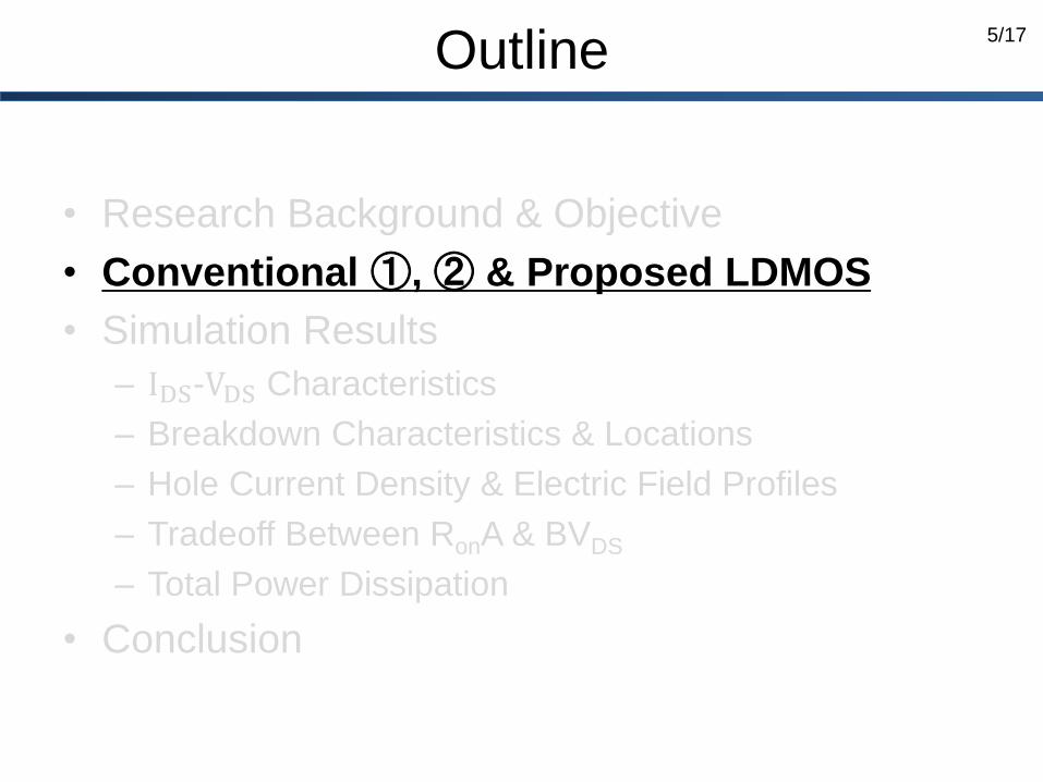
• Research Background & Objective
• Conventional ①, ② & Proposed LDMOS
• Simulation Results
– IDS-VDS Characteristics
– Breakdown Characteristics & Locations
– Hole Current Density & Electric Field Profiles
– Tradeoff Between RonA & BVDS
– Total Power Dissipation
• Conclusion
6/17
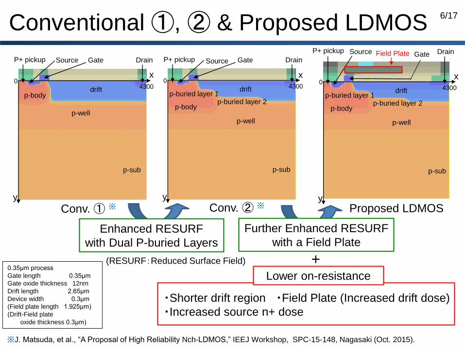
Conventional ①, ② & Proposed LDMOS
drift
p-well
p-sub
p-body
Source Gate Drain
y
x0
4300
P+ pickup
Conv. ① ※
drift
p-well
p-sub
p-body
y
x0
4300
p-buried layer 1p-buried layer 2
Conv. ② ※
Gate DrainP+ pickup Source
・Shorter drift region
・Increased source n+ dose
・Field Plate (Increased drift dose)
drift
p-well
p-sub
p-body
y
x0
4300
p-buried layer 1p-buried layer 2
Gate DrainP+ pickup Source Field Plate
Proposed LDMOS
0.35μm process
Gate length 0.35μm
Gate oxide thickness 12nm
Drift length 2.65μm
Device width 0.3μm
(Field plate length 1.925μm)
(Drift-Field plate
oxide thickness 0.3μm)
Lower on-resistance
+
Further Enhanced RESURF
with a Field PlateEnhanced RESURF
with Dual P-buried Layers
(RESURF:Reduced Surface Field)
※J. Matsuda, et al., “A Proposal of High Reliability Nch-LDMOS,” IEEJ Workshop, SPC-15-148, Nagasaki (Oct. 2015).
7/17
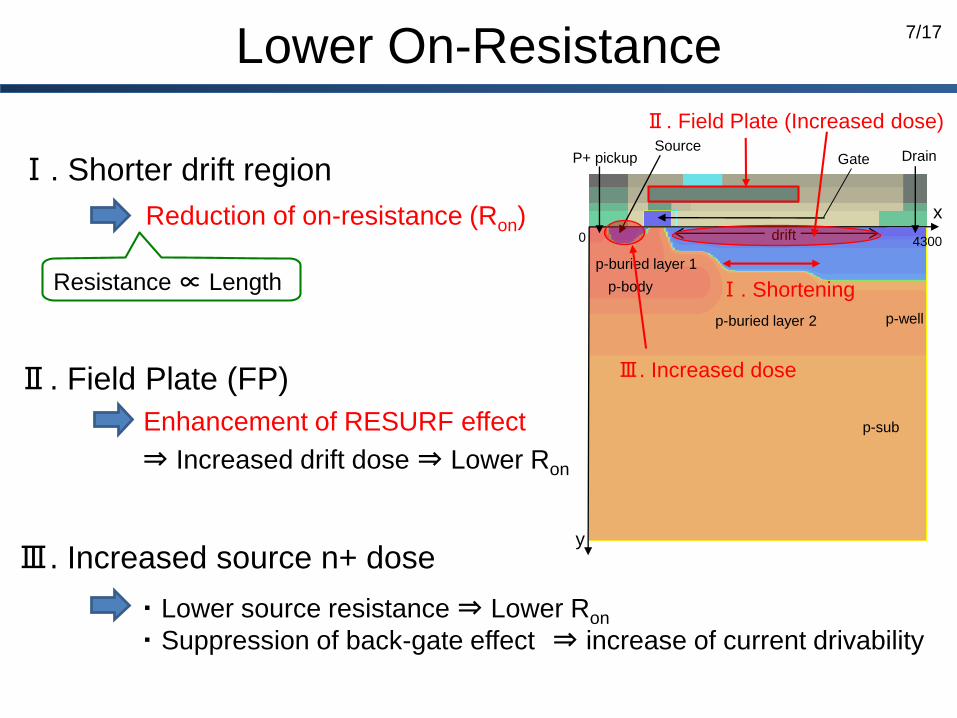
Lower On-Resistance
Ⅰ. Shorter drift region
Ⅱ. Field Plate (FP)
Reduction of on-resistance (Ron)
Enhancement of RESURF effect
⇒ Increased drift dose ⇒ Lower Ron
Resistance∝ Length
・ Lower source resistance ⇒ Lower Ron
・ Suppression of back-gate effect ⇒ increase of current drivability
Ⅲ. Increased source n+ dose
p-buried layer 1
p-sub
p-body
SourceGate Drain
y
0 4300
P+ pickup
p-wellp-buried layer 2
Ⅱ. Field Plate (Increased dose)
drift
x
Ⅰ. Shortening
Ⅲ. Increased dose
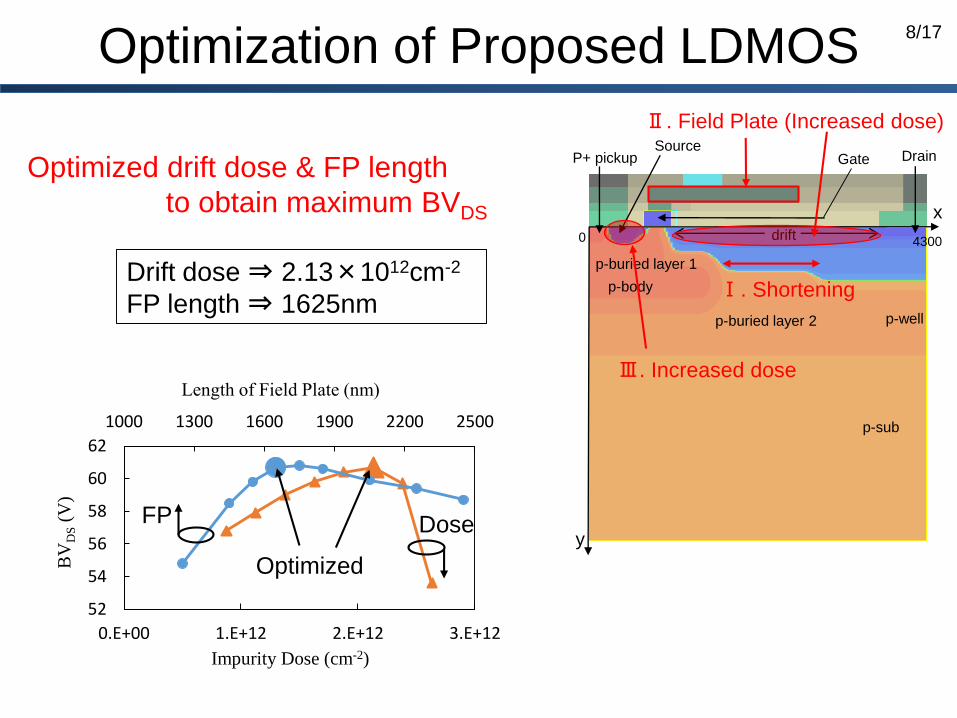
8/17
1000 1300 1600 1900 2200 2500
52
54
56
58
60
62
0.E+00 1.E+12 2.E+12 3.E+12
Length of Field Plate (nm)
BV
DS
(V)
Impurity Dose (cm-2)
Optimization of Proposed LDMOS
Optimized drift dose & FP length
to obtain maximum BVDS
Optimized
Drift dose ⇒ 2.13×1012cm-2
FP length ⇒ 1625nm
FP Dose
p-buried layer 1
p-sub
p-body
SourceGate Drain
y
0 4300
P+ pickup
p-wellp-buried layer 2
Ⅱ. Field Plate (Increased dose)
drift
x
Ⅰ. Shortening
Ⅲ. Increased dose
9/17
Outline
• Research Background & Objective
• Conventional ①, ② & Proposed LDMOS
• Simulation Results*
– 𝐈𝐃𝐒-𝐕𝐃𝐒 Characteristics
– Breakdown Characteristics & Locations
– Hole Current Density & Electric Field Profiles
– Tradeoff Between RonA & BVDS
– Total Power Dissipation
• Conclusion*Simulator: 3D TCAD (Device Simulator: Advance/DESSERT)
Developed by AdvanceSoft Corporation, Japan
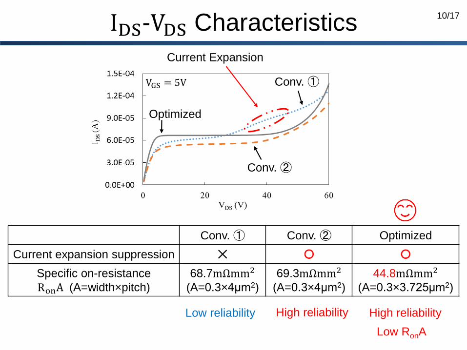
10/17IDS-VDS Characteristics
Current Expansion
Conv. ①
Conv. ②
Optimized
Conv. ① Conv. ② Optimized
Current expansion suppression ✕ 〇 〇
Specific on-resistance
RonA (A=width×pitch)
68.7mΩmm2
(A=0.3×4μm2)
69.3mΩmm2
(A=0.3×4μm2)
44.8mΩmm2
(A=0.3×3.725μm2)
Low reliability High reliability
Low RonA
High reliability
VGS = 5V
11/17
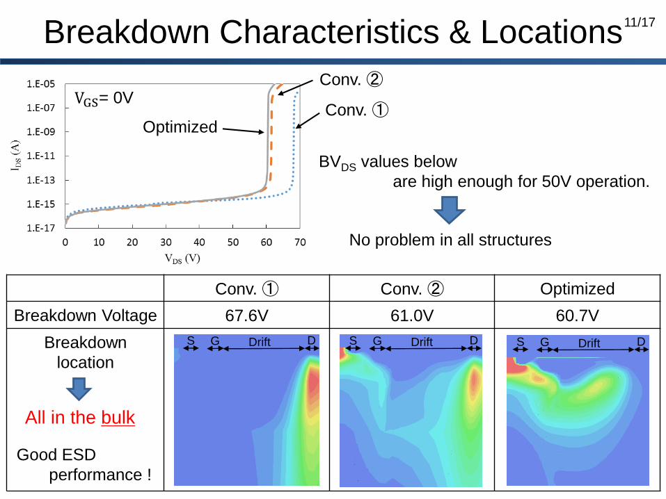
Conv. ① Conv.② Optimized
Breakdown Voltage 67.6V 61.0V 60.7V
Breakdown
location
Breakdown Characteristics & Locations
DDriftGS DDriftGS DDriftGS
Conv. ①
Conv. ②
Optimized
VGS= 0V
BVDS values below
are high enough for 50V operation.
All in the bulk
Good ESD
performance !
No problem in all structures
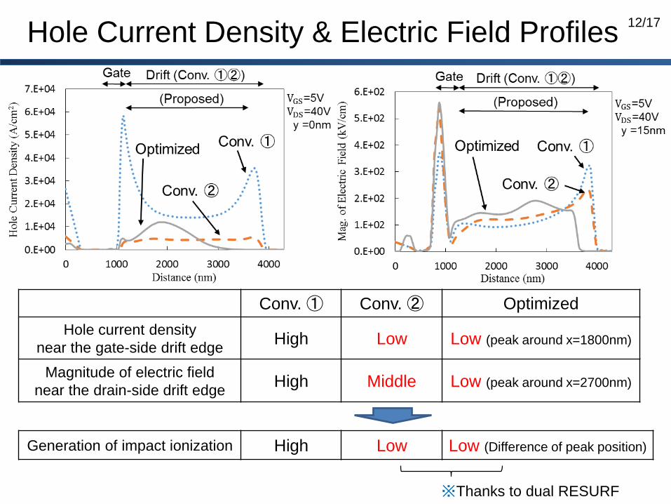
12/17Hole Current Density & Electric Field Profiles
Conv. ① Conv. ② Optimized
Hole current density
near the gate-side drift edgeHigh Low Low (peak around x=1800nm)
Magnitude of electric field
near the drain-side drift edgeHigh Middle Low (peak around x=2700nm)
Generation of impact ionization High Low Low (Difference of peak position)
※Thanks to dual RESURF
13/17
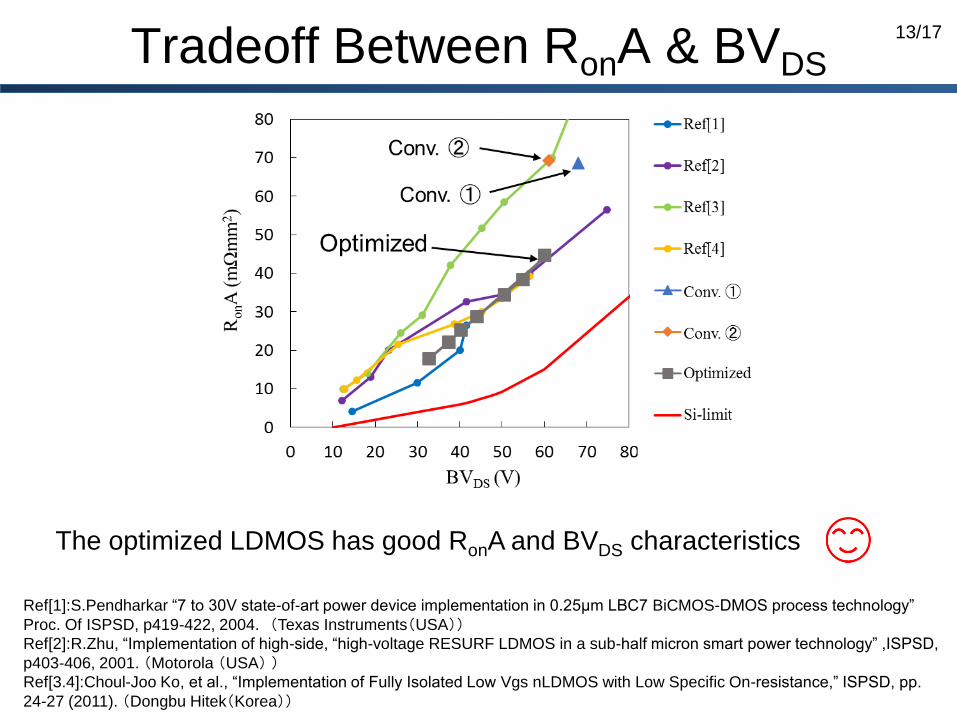
Tradeoff Between RonA & BVDS
Ref[1]:S.Pendharkar “7 to 30V state-of-art power device implementation in 0.25μm LBC7 BiCMOS-DMOS process technology”
Proc. Of ISPSD, p419-422, 2004. (Texas Instruments(USA))Ref[2]:R.Zhu, “Implementation of high-side, “high-voltage RESURF LDMOS in a sub-half micron smart power technology” ,ISPSD,
p403-406, 2001. (Motorola (USA) )Ref[3.4]:Choul-Joo Ko, et al., “Implementation of Fully Isolated Low Vgs nLDMOS with Low Specific On-resistance,” ISPSD, pp.
24-27 (2011). (Dongbu Hitek(Korea))
The optimized LDMOS has good RonA and BVDS characteristics
14/17
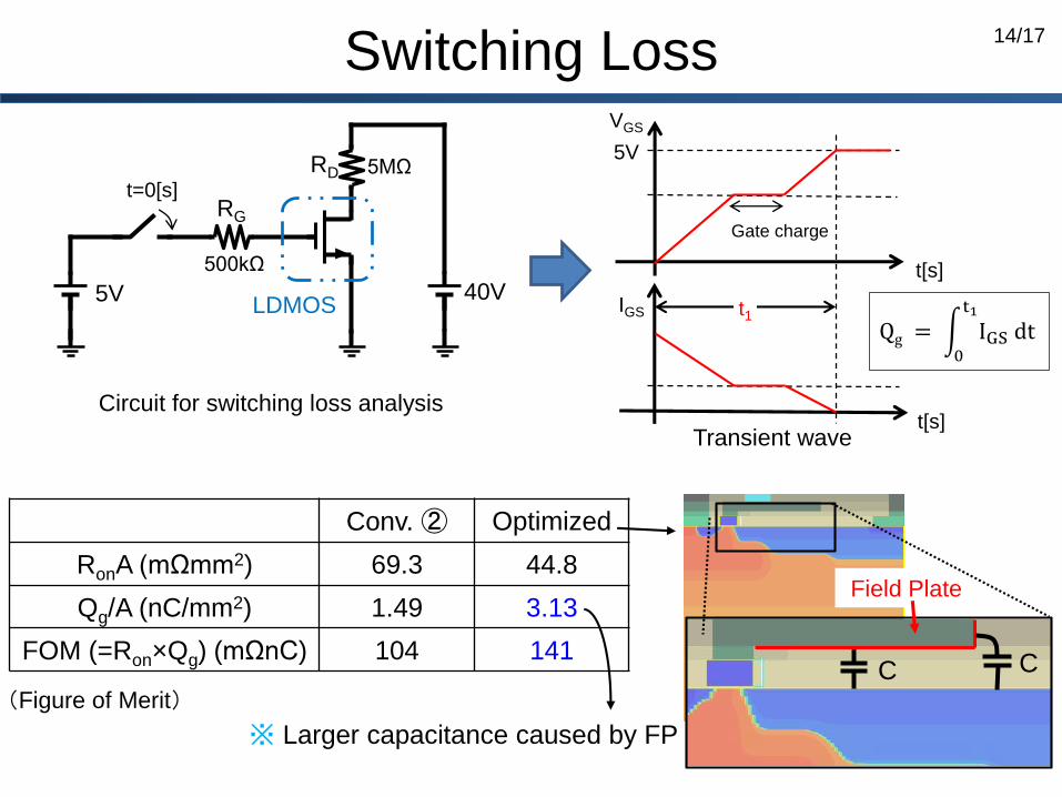
Switching Loss
5V 40V
RD
RG
LDMOS
500kΩ
5MΩt=0[s]
Circuit for switching loss analysis
Transient wave
Qg = 0
t1
IGS dt
t[s]
5V
VGS
IGS
t[s]
t1
Conv. ② Optimized
RonA (mΩmm2) 69.3 44.8
Qg/A (nC/mm2) 1.49 3.13
FOM (=Ron×Qg) (mΩnC) 104 141
Gate charge
※ Larger capacitance caused by FP
Field Plate
C C
(Figure of Merit)
15/17
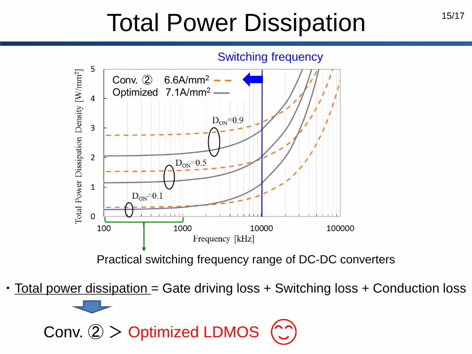
Total Power Dissipation
・ Total power dissipation = Gate driving loss + Switching loss + Conduction loss
Practical switching frequency range of DC-DC converters
Conv. ②> Optimized LDMOS
Switching frequency

16/17
Outline
• Research Background & Objective
• Conventional ①, ② & Proposed LDMOS
• Simulation Results
– IDS-VDS Characteristics
– Breakdown Characteristics & Locations
– Hole Current Density & Electric Field Profiles
– Tradeoff Between RonA & BVDS
– Total Power Dissipation
• Conclusion
17/17
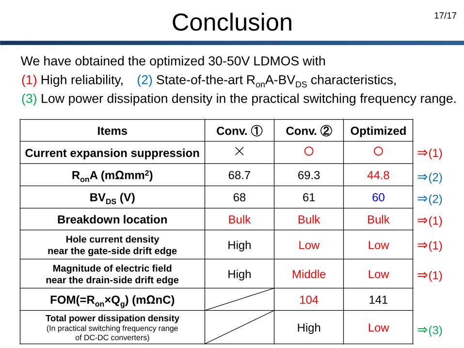
Conclusion
Items Conv. ① Conv. ② Optimized
Current expansion suppression ✕ 〇 〇
RonA (mΩmm2) 68.7 69.3 44.8
BVDS (V) 68 61 60
Breakdown location Bulk Bulk Bulk
Hole current density
near the gate-side drift edgeHigh Low Low
Magnitude of electric field
near the drain-side drift edgeHigh Middle Low
FOM(=Ron×Qg) (mΩnC) 104 141
Total power dissipation density(In practical switching frequency range
of DC-DC converters) High Low
⇒(1)
⇒(1)
⇒(1)
⇒(1)
⇒(2)
⇒(3)
⇒(2)
We have obtained the optimized 30-50V LDMOS with
(1) High reliability, (2) State-of-the-art RonA-BVDS characteristics,
(3) Low power dissipation density in the practical switching frequency range.
18/17
Acknowledgement
We would like to express sincere thanks to AdvanceSoft Corporation
for lending us 3D TCAD simulator.
The 3D TCAD developed by AdvanceSoft Corporation was assisted
by A-STEP program of Japan Science and Technology Agency,
National Research and Development Agency.
19/17
Appendix
20/17
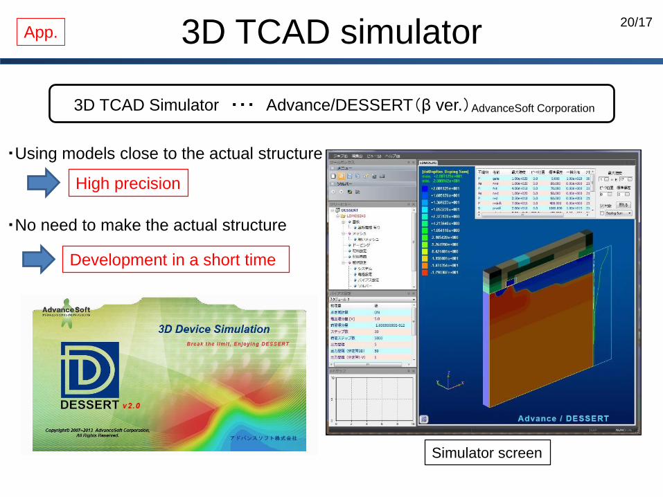
3D TCAD simulator
High precision
・Using models close to the actual structure
・No need to make the actual structure
Development in a short time
3D TCAD Simulator ・・・ Advance/DESSERT(β ver.)AdvanceSoft Corporation
Simulator screen
App.
21/17
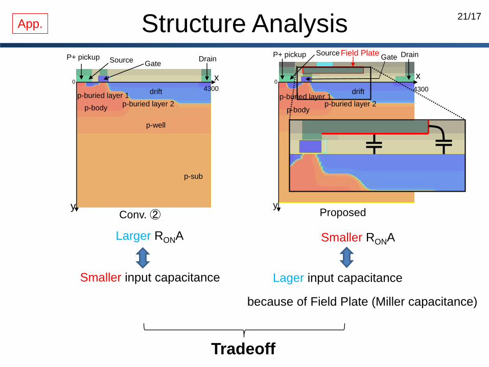
Structure Analysis
drift
p-well
p-sub
p-body
SourceGate
Drain
y
x0
4300
P+ pickup
p-buried layer 1p-buried layer 2
Field Plate
drift
p-well
p-sub
p-body
SourceGate Drain
y
x0
4300
P+ pickup
p-buried layer 1p-buried layer 2
Conv. ② Proposed
Larger RONA
Smaller input capacitance
Smaller RONA
Lager input capacitance
App.
because of Field Plate (Miller capacitance)
Tradeoff
22/17
Detail of Dissipation
PSW[w]
Period
DON DOFF
IDS×VDS
t[s]
Switching loss ①
Switching loss ②
LDMOS
Driver
ON
OFF
Rdri.ON
Rdri.OFF
ID×VD
t[s]
ID
VD
VDS
IDS
Gate drive loss Switching loss
ON1
2𝐶𝑉2
OFF1
2𝐶𝑉2
Period 𝐶𝑉2
𝑄 = 𝐶𝑉
Switching loss ①(Switching mode)
Switching loss②(Conductive mode)
Frequency dependence Duty ratio dependence
𝑓 × 𝑄𝑔𝑉𝐺𝑆 𝐷𝑂𝑁 × 𝐼𝐷𝑆𝑉𝐷𝑆Total power
dissipation [w]= + +𝑓 × 2 𝑖𝑑𝑠𝑣𝑑𝑠𝑑𝑡
𝑡𝑢𝑟𝑛_𝑂𝑁
Area of triangleON-time
App.
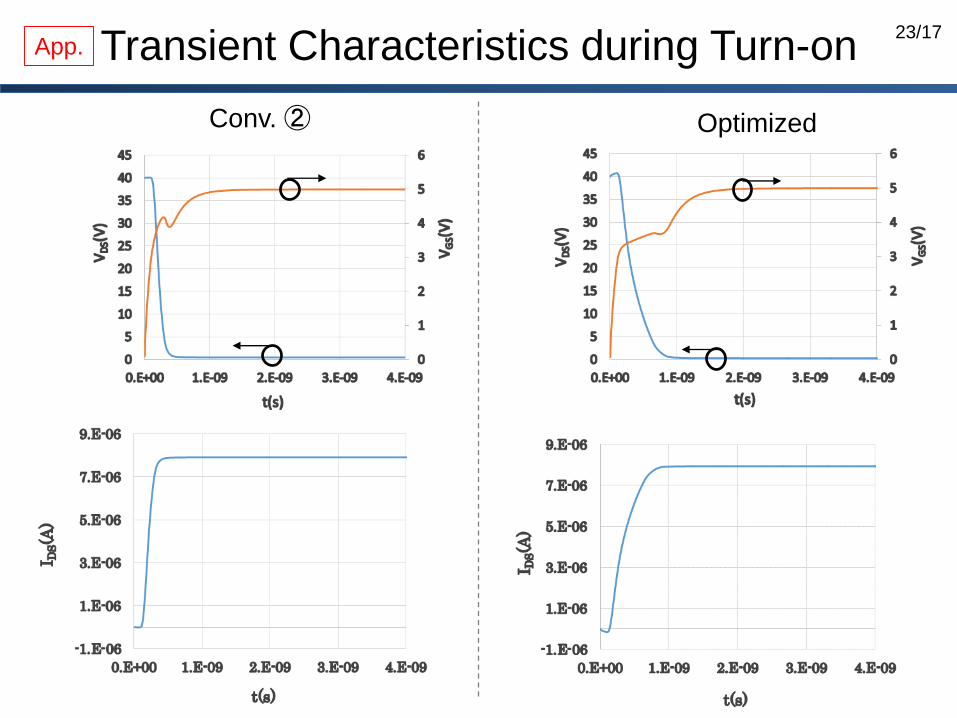
23/17Transient Characteristics during Turn-on
Conv. ② Optimized
App.
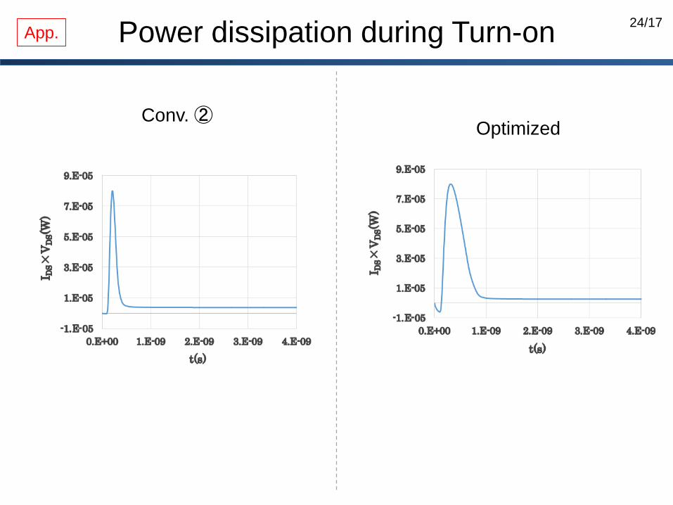
24/17Power dissipation during Turn-on
Conv. ②Optimized
App.
25/17
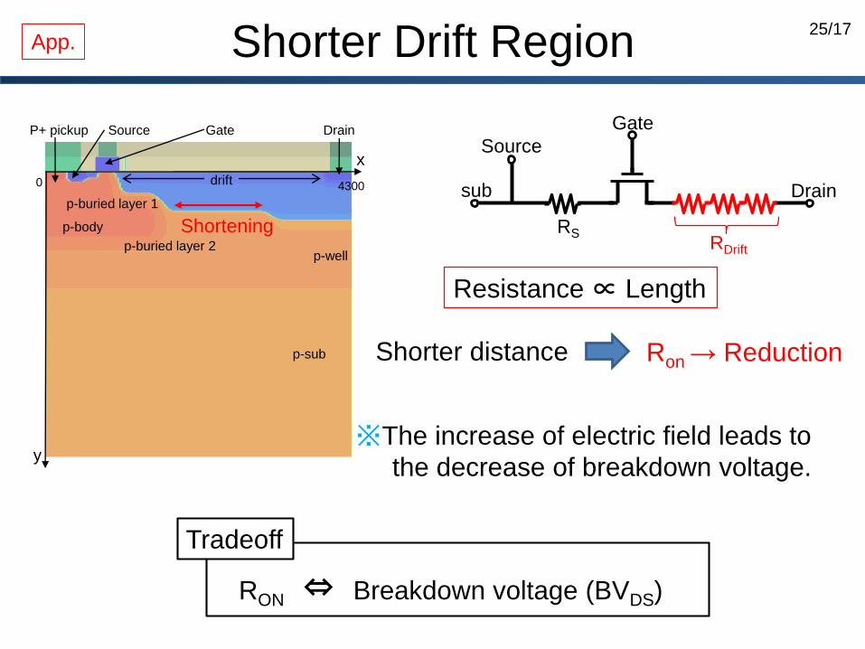
Shorter Drift Region
RSRDrift
sub
Source
Gate
Drain
※The increase of electric field leads to
the decrease of breakdown voltage.
Resistance∝ Length
drift
p-buried layer 1
p-sub
p-body
Source Gate Drain
y
x
0 4300
P+ pickup
p-wellp-buried layer 2
Ron → ReductionShorter distance
RON ⇔ Breakdown voltage (BVDS)
Tradeoff
App.
Shortening
26/17
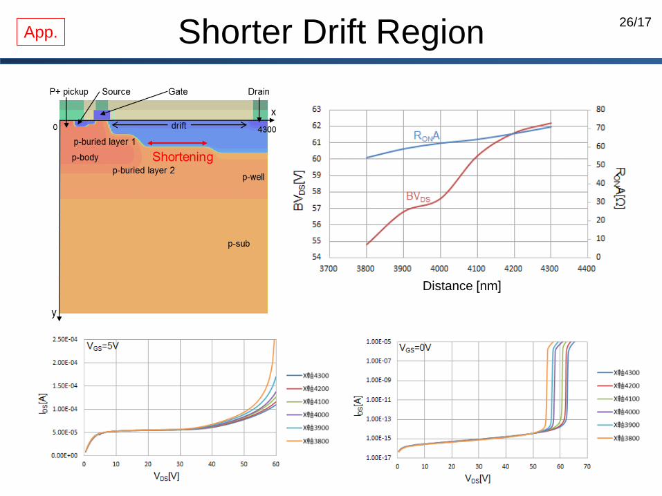
Shorter Drift Region
Distance [nm]
App.
27/17
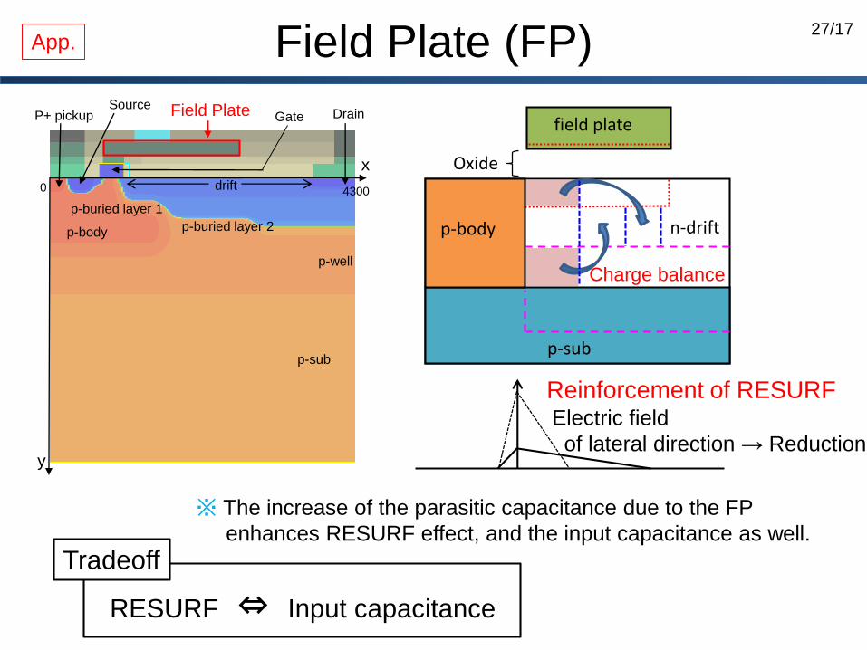
Field Plate (FP)
※ The increase of the parasitic capacitance due to the FP
enhances RESURF effect, and the input capacitance as well.
Reinforcement of RESURF
n-drift
p-sub
field plate
Charge balance
Oxide
p-body
Electric field
of lateral direction → Reduction
p-buried layer 1
p-sub
p-body
SourceGate Drain
y
0 4300
P+ pickup
p-well
p-buried layer 2
Field Plate
drift
x
RESURF ⇔ Input capacitance
Tradeoff
App.
28/17
p-buried layer 1
p-sub
p-body
SourceGate Drain
y
0 4300
P+ pickup
p-well
p-buried layer 2
drift
x
Increased Source & Drift Dose
RSRDrift
sub
Source
Gate
Increased dose
Carrier → Increased
IDS(A)
VDS(V)
Current → Increased
Ron → Reduction
Drain
Due to
source resistance
Due to drift resistance
App.
Increased dose
※ Suppression of back-gate effect
29/17
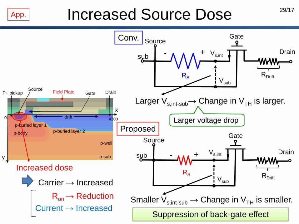
Increased Source Dose
Carrier → Increased
p-buried layer 1
p-sub
p-body
SourceGate Drain
y
0 4300
P+ pickup
p-well
p-buried layer 2
Field Plate
drift
x
Current → Increased
Ron → Reduction
Larger Vs,int-sub→ Change in VTH is larger.
RSRDrift
sub
SourceGate
DrainVs,int
Vsub
+-
RS RDrift
sub
SourceGate
DrainVs,int
Vsub
+-
Smaller Vs,int-sub → Change in VTH is smaller.
Proposed
Conv.
Larger voltage drop
Increased dose
Suppression of back-gate effect
App.
30/17
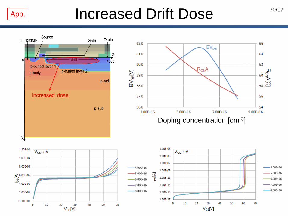
Increased Drift DoseApp.
Doping concentration [cm-3]
31/17
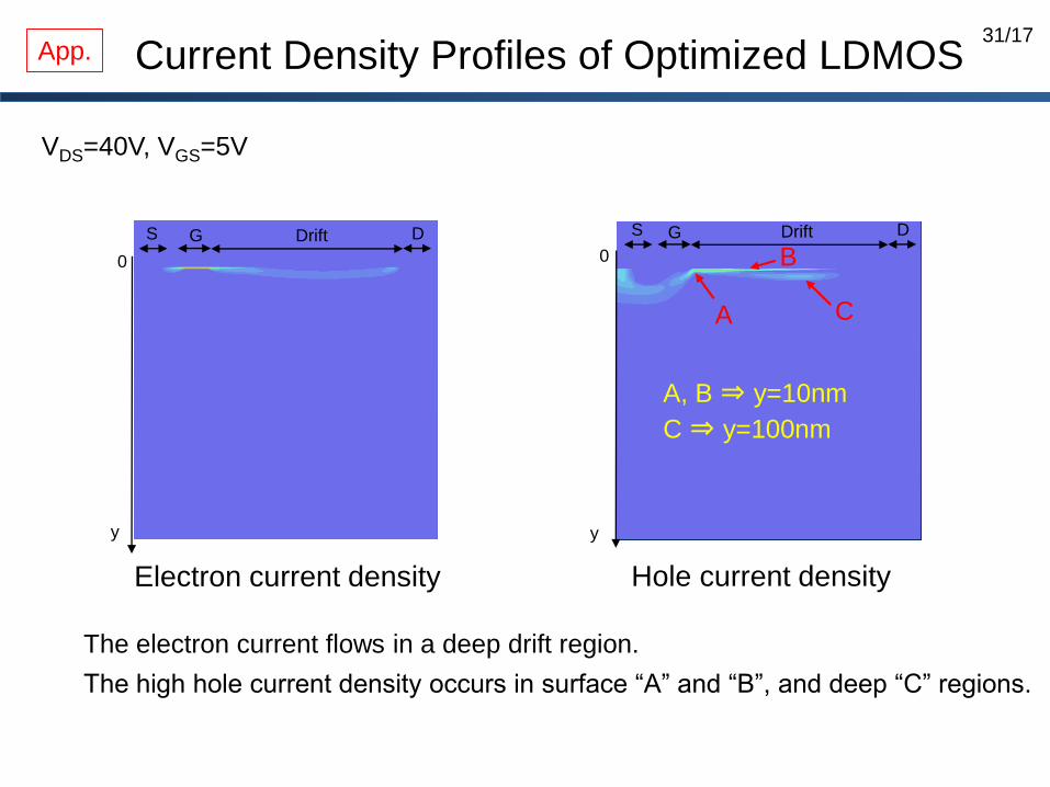
Current Density Profiles of Optimized LDMOS
DDriftGS
A, B ⇒ y=10nm
C ⇒ y=100nm
Electron current density Hole current density
DDriftGS
VDS=40V, VGS=5V
0 0
y y
The high hole current density occurs in surface “A” and “B”, and deep “C” regions.
App.
A C
B
The electron current flows in a deep drift region.
32/17
Hole/Electron Current Density & Electric Field Profiles
Optimized
VDS=40V, VGS=5V
(a)
App.
High electron current density & electric field generate holes.
A
B
The holes in the shallow “B” region mainly comes from the deep “C” region.
A
The hot carriers generated in the “A” region would degrade MOSFET characteristics.
y=10nm y=10nm
Hole current by impact ionization
∝(electron current)×(electric field)×exp(-A/electric field)
33/17
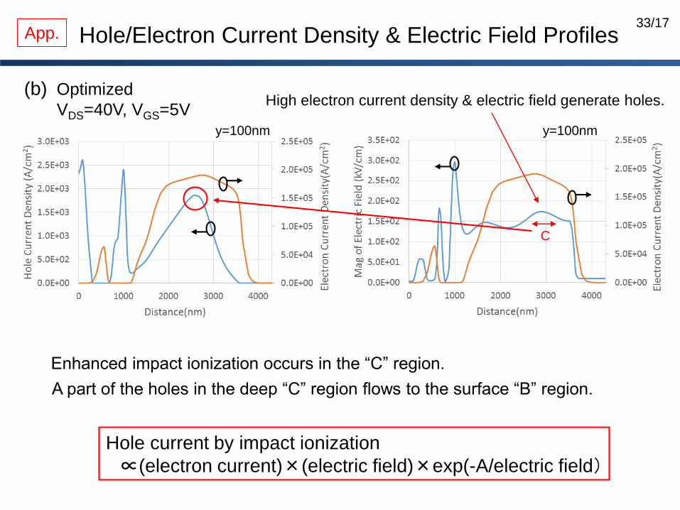
(b) Optimized
VDS=40V, VGS=5V
App.
Hole current by impact ionization
∝(electron current)×(electric field)×exp(-A/electric field)
High electron current density & electric field generate holes.
C
Enhanced impact ionization occurs in the “C” region.
A part of the holes in the deep “C” region flows to the surface “B” region.
y=100nm y=100nm
Hole/Electron Current Density & Electric Field Profiles
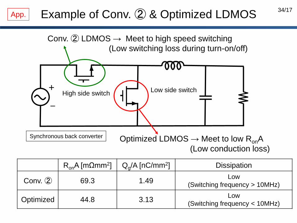
34/17Example of Conv. ② & Optimized LDMOS
+
Optimized LDMOS → Meet to low RonA
(Low conduction loss)
Conv. ② LDMOS → Meet to high speed switching
(Low switching loss during turn-on/off)
RonA [mΩmm2] Qg/A [nC/mm2] Dissipation
Conv. ② 69.3 1.49Low
(Switching frequency > 10MHz)
Optimized 44.8 3.13Low
(Switching frequency < 10MHz)
High side switchLow side switch
App.
Synchronous back converter
35/17
Q1. 耐圧などはシミュレーションでどれほどの精度があるのか。
A1. We used a device simulator, DESSERT. This simulator can analyze
device characteristics with high precision using latest and proven physical
models. So, simulation results can be basically accurate.
Q3.製造のときにフィールドプレートや層のズレがあると思うが、耐圧とかは下がらないのか。
A3. If the amount of misalignment for the field plate and p-buried layers is less
than ±10%, the value of the breakdown voltage remains almost constant.
A2. The LDMOS can be made based on a conventional 0.35μm CMOS
process. So, the fabrication of the LDMOS would not be complicated.
Q2.実際に作ったらどうか。
App.
36/17
Q & A
Q1: p.11の下の画像は実測なのか?
A1: 実測ではない。シミュレーションのみの結果である。
Q2: p.11に”good ESD performance“とあるが、なぜか?
A2: バルクでブレークダウンが発生しており、ゲートでは発生していないから。
(上のように答えましたが、質問者は何度も質問し、その質問を私は正確に聞き取ることができませんでした。発表後、築地さんに尋ねたところ、質問者はBVDSのことをD-S間ではなくG-S間と勘違いしていたそうです。)
発表日:2016/10/27
37/36