Embed Size (px)
Citation preview

OpenREPORT 1 (43)
Prepared (also subject responsible if other) No.
ERA/X/L Ulf Olin ERA/X/L-00:027 UenApproved Checked Date Rev Reference
ERA/X/L (Ulf Olin) 2000-10-23 A
Optical interconnection technology in switches,routers and optical cross connects
Magnus Jonsson and Ulf Olin1
School of Information Science, Computer and Electrical Engineering,Halmstad University, Halmstad, Sweden, Box 823, S-301 18, Sweden
[email protected], http://www.hh.se/ide
1 Ericsson Generic Technologies, ERA/X/L164 80 Stockholm
Abstract
The performance of data- and telecommunication equipment must keep upwith the increasing network speed. Moreover, to allow more input andoutput ports on such equipment, the internal interconnection complexityoften grows exponentially with the number of ports. Therefore, newinterconnection technologies to be used internally in the equipment areneeded. Optic interconnection technology is a promising alternative and alot of work has been done. In this report, a number of optical andoptoelectronic interconnection architectures are reviewed, especially froma data- and telecommunication equipment point-of-view. Three kinds ofsystems for adoption of optical interconnection technology are discussed:(i) optical cross connects (OXCs), (ii) switches and routers with some kindof burst switching, and (iii) switches and routers which redirect traffic onthe packet or cell level. The reviewed interconnection technologies andarchitectures are discussed according to their suitability of adoption in thethree mentioned systems.
The annex summarises manufacturers of devices required for opticalinterconnects and backplanes, and needs for optical interconnectiontechnology in future Ericsson systems.
Keyword
Optical backplanes, optical interconnects, VCSELs, fibre-ribbon cables

OpenREPORT 2 (43)
Prepared (also subject responsible if other) No.
ERA/X/L Ulf Olin ERA/X/L-00:027 UenApproved Checked Date Rev Reference
ERA/X/L (Ulf Olin) 2000-10-23 A
Contents
1 Introduction 22 Electronic switches and routers 32.1 Circuit switching 42.2 Packet switching 42.3 Switch fabrics 53 Optical link technologies 73.1 Fibre-ribbon links 83.2 Bit-parallel WDM links 103.3 Reliability of optoelectronics 103.4 Major research activities 114 Fibre-optic interconnection networks 124.1 Passive fibre-optic networks 124.2 WDM star 154.3 WDM ring 164.4 Fibre-ribbon pipeline ring network 175 Integrated optical interconnection systems 185.1 Integrated fibre and waveguide solutions 195.2 Planar free space optics 205.3 Free space optical backplanes 216 Optical and optoelectronic switch-fabrics 226.1 Optical interconnections and electronic crossbars 226.2 WDM/SDM switches 237 Commercial system implementations 247.1 Sycamore 247.2 Pluris 257.3 Sirocco Systems 257.4 InfiniBand Trade Association 258 Conclusions 259 References 2710 Annex 3810.1 Commercial solutions 3810.2 Demands from future Ericsson products 43
1 Introduction
Novel optical technologies result in the possibility of new solutions for theincreasing bandwidth demands of data communication andtelecommunication equipment. In this report, we explore the possibilities,from an architectural and a device perspective, of using opticalinterconnections in such equipment. Although there exist many otheroptical interconnection architectures that might be candidates, only someselected groups or concepts are selected here to give a reasonably broadview of possible solutions.

OpenREPORT 3 (43)
Prepared (also subject responsible if other) No.
ERA/X/L Ulf Olin ERA/X/L-00:027 UenApproved Checked Date Rev Reference
ERA/X/L (Ulf Olin) 2000-10-23 A
The interconnection architectures are evaluated according to three types ofsystems, which mostly varies in terms of switching time requirements. Thesystems are: (i) optical cross connects (OXCs), (ii) switches and routerswith some kind of burst switching, and (iii) switches and routers whichredirect traffic on the packet or cell level.
OXCs have relatively slow timing requirements, i.e., in the order ofmilliseconds or even tens of milliseconds. On the other hand, it is valuableif the signals remain optical all the way through the switch includingpossible queuing systems, i.e., having optical transparency. In this way it iseasier to scale up the bit rate or change protocols.
When using burst switching, packets with the same destination (e.g., thesame exterior gateway) can be grouped together to reduce switching timerequirements. This has, for instance, been discussed for use in all opticalpacket switching [Callegati et al. 1999] [Turner 1999]. The switching timerequirements are in the order of sub-microseconds.
For pure switching at the packet or cell level, the switching timerequirements are in the order of a nanosecond. With longer switchingtimes, the overhead between each packet will be too large. All-opticalpacket switching has been proposed but is far from a mature technology[Callegati et al. 1999]. However, some experiments have been done[Blumenthal et al. 1999] [Chiaroni et al. 1998]. Another driving applicationdomain for optical system-level interconnections, in addition to data- andtelecommunication equipment, is parallel and distributed computingsystems.
The rest of the report is organised as follows. Electronic switches androuters are briefly reviewed in Section 2. In Section 3, optical linktechnologies are described, and in Section 4, fibre-optic interconnectionnetworks are presented. Integrated optical interconnection systems andoptical and optoelectronic switch-fabrics are presented in Sections 5 and 6,respectively. The report is then concluded in Section 7. The annexessummarise commercial devices of interest for optical backplanes andinterconnects and the needs from Ericsson product units for opticalinterconnects and backplanes.
2 Electronic switches and routers
Data communication networks can be divided into circuit switching andpacket switching networks. These two categories will be treated inSubsections 2.1 and 2.2, respectively. Then, in Subsection 2.3, switchfabrics to be used as the core switching part of networking equipment willbe discussed.

OpenREPORT 4 (43)
Prepared (also subject responsible if other) No.
ERA/X/L Ulf Olin ERA/X/L-00:027 UenApproved Checked Date Rev Reference
ERA/X/L (Ulf Olin) 2000-10-23 A
2.1 Circuit switching
When using circuit switching, a "physical" channel is allocated before thecommunication between a pair of nodes can start. The "physical" channeldoes not need to be a purely physical but can, e.g., be a cyclicallyavailable time slot on a time multiplexed channel, i.e., Time DivisionMultiplexing (TDM). SDH is an example of a communication standard thatrelies on TDM. The advantage of circuit switching is the guaranteedbandwidth, while disadvantages are long set-up times and low bandwidthutilisation when the channel is idle for a long time, since the bandwidthnormally cannot be reused.
Figure 1: Some wavelengths can be dropped and/or added, while otherwavelengths just pass through.
The switching time requirements for circuit switching networks are typicallynot so demanding because of the duration of channels. However, in, e.g.,an SDH Add-Drop Multiplexer (ADM), all traffic (including bypassing traffic)must be electronically processed in some sense. It can, for instance, beneeded to be able to separate traffic with different destinations (e.g., bedropped or pass) from different time slots. By multiplexing in thewavelength domain instead of the time domain, a wavelength only carryingtraffic which should pass do not have to be processed at all (see Figure 1).
2.2 Packet switching
When using packet switching, the data to be transferred are split intopackets that compete for bandwidth with packets from other nodes. Trafficsituations with temporary bursts of large volumes of data from one or a fewsources can therefore be handled better in a packet-switched network thanin the case that much of the bandwidth is allocated by other nodes usingcircuit switching. Also, sporadic traffic often experiences a shorter latencythan in the case that a circuit must be set-up each time. Handling real-timetraffic is, however, harder in a packet-switched network. Two main kinds ofpacket switches are ATM switches and IP routers.
Packet switches can be built in a number of ways for which we here willgive two examples of architectures. The first packet switch architectureconsist of input interfaces, input queues, switch fabric, output queues, andoutput interfaces, where some or all of the listed units are coupled to acentral control unit (see Figure 2). The main function of the control unit isto configure the switch fabric to pass packets queued in the input queuesto the correct output queues, based on some routing decision. Otherqueuing strategies are possible too, e.g., only at the input side or theoutput side, a larger shared queuing memory, or internally in the switchfabric.

OpenREPORT 5 (43)
Prepared (also subject responsible if other) No.
ERA/X/L Ulf Olin ERA/X/L-00:027 UenApproved Checked Date Rev Reference
ERA/X/L (Ulf Olin) 2000-10-23 A
Switchfabric
Control unit
Figure 2: An example of switch architecture.
One of the simplest ways to implement a switch fabric is to have a sharedmedium to which I/O interfaces or similar are attached. A common way ofimplementing a shared-medium network is to use the bus topology, but itcan also be, e.g., a ring where only one node is allowed to send at a time.The great advantage of a shared-medium network is the easyimplementation of broadcast, which is useful in many situations. Thedisadvantage is that the bandwidth does not scale at all with the number ofnodes.
The second example of a packet switch architecture is a bus to which I/O-interfaces and a control unit (routing processor), or units, are connected(see Figure 3). Incoming packets are transferred from an I/O interface tothe control unit. The control unit makes routing decisions or similar andredirects each packet to the correct I/O interface for transmission out onthe network again. Sometimes, the I/O interfaces have enough intelligenceto redirect packets directly to the destination I/O interface, at least for somekind of traffic. More information on switch and router architectures is foundin [Kou 1999].
Control unit(e.g., routingprocessor)
Figure 3: Bus-based switch architecture.
2.3 Switch fabrics
The crossbar is the most flexible switch fabric and can be compared with afully connected topology, i.e., point-to-point connections between allpossible combinations of two nodes. The drawback, however, is theincrease by N2 in cost/complexity of the switch, where N is the number ofports. Systems with a single true crossbar are therefore limited to smallsystems.

OpenREPORT 6 (43)
Prepared (also subject responsible if other) No.
ERA/X/L Ulf Olin ERA/X/L-00:027 UenApproved Checked Date Rev Reference
ERA/X/L (Ulf Olin) 2000-10-23 ATransmitter side Receiver side
Figure 4: Omega network for an eight-node system. One path through thenetwork is highlighted.
In multistage shuffle-exchange networks, the cost function is reduced toN log2 N, but where log2 N stages must be traversed to reach the desiredoutput port. An example of such a network is the Omega network (Figure4) which provides exactly one path from every input to every output. Thefour different switch functions of the 2 × 2 switch that is used as buildingblock are shown in Figure 5, where the two rightmost configurations areused for broadcast. Switches larger than 2 × 2 can also be used. Eachstage of the switches in an Omega network is preceded by a perfect-shuffle pattern. In contrast to a crossbar network, which is a nonblockingnetwork, an Omega network is a blocking network. This means that theremight not always exist a path through the network as a result of alreadyexisting paths that block the way.
Figure 5: Possible states of a 2 × 2 switch.
Rearrangeable networks are another category of multistage networkswhere it is always possible to find a path through the network. However, ifnot all paths are routed at the same time, it may be necessary to reroutealready existing paths. An example of a rearrangeable network is theBenes network shown in Figure 6. Other multistage networks includeBanyan networks [Goke and Lipovski 1973].
Figure 6: A rearrangeable Benes network.
OpenREPORT 7 (43)
Prepared (also subject responsible if other) No.
ERA/X/L Ulf Olin ERA/X/L-00:027 UenApproved Checked Date Rev Reference
ERA/X/L (Ulf Olin) 2000-10-23 A
3 Optical link technologies
Historically, the use of optical fibres for signal interconnection began withthe simplest level of point-to-point fibres in telecommunications long-haulnetworks. However, today, as the complexity and the bit rates increase inswitching and routing equipment, optical interconnects are starting to beimplemented in the equipment building practice to satisfy the distance andbandwidth requirements.
Connections are usually made from the optoelectronics on printed wiringboards or cards to those on other boards on the same or other shelves.Other types of optical interconnections are between cabinets ofmulticabinet equipment (such as digital crossconnect switches) or betweenthe central processing units and remote memories of high-performanceworkstations and computers.
According to ElectroniCast Corp. [Montgomery 2000] the market for opticalbackplanes is expected to grow from a total of $6.1 million in 1998 to $125million in 2003 and $1 647 million in 2008. In 1998, two thirds of the totalglobal demand of optical backplanes came from telecom transportterminals and switches.
The potential advantages with optical interconnects are that
• Higher interconnect bit rate per circuit area can be achieved
• Noise is not generated as for wire interconnects
• Scaleable interconnection bandwidths are possible
• The low loss in waveguides and free-space makes longer connectionspossible
Today, for high data rate (100’s of Mbps to over 1 Gbps) electricalconnections, twinned-pair LVDS (Low Voltage Differential Signalling) andrelated technologies are used. With improved impedance matchingbetween the driver and termination circuits and the cable, data rates up to2-4 Gbps are anticipated to be achieved. For short distances, 0,5 – 1 m,also bit rates up to 10 Gb/s are considered using new board materials.
In the table below is shown a comparison between a commercial paralleloptical fibre transmitter [Mitel] with 12 channels, each operating at 2.5Gbps, and a 400 Mbps serial bus LVDS circuit [National]. The last columnshows a few years old goals from a DARPA program on opticalinterconnection technologies [Towe]. It is evident that today’s VCSEL-based fibre ribbon cable technology has properties comparable to those ofelectrical interconnections, when the full capacity of the fibre-ribbon linksare utilised.

OpenREPORT 8 (43)
Prepared (also subject responsible if other) No.
ERA/X/L Ulf Olin ERA/X/L-00:027 UenApproved Checked Date Rev Reference
ERA/X/L (Ulf Olin) 2000-10-23 A
VCSELarray
LVDScircuit
DARPAgoals 1997
Price/data rate ($ / Gb/s) 14.7 18.8 10
Data rate/circuit area (Gb/s /cm2)
4 0.07 10
Data rate/power consumption(Gb/s / W)
15.8 3.8 20
Below, two main categories of optical link technologies are discussed,fibre-ribbon links (Subsection 3.1) and bit-parallel WDM links (Subsection3.2). Single-channel single-fibre solutions are not treated.
3.1 Fibre-ribbon links
A system component that has reached the market recently [Bursky 1994][Fibre Systems 1998] is the fibre-ribbon link [Buckman et al. 1998][Engebretsen et al. 1996] [Hahn 1995] [Hahn 1995B] [Hahn et al. 1996][Hartman et al. 1990] [Jiang et al. 1998] [Karstensen et al. 1995][Karstensen et al. 1998] [Kuchta et al. 1998] [Nagarajan et al. 1998][Nishimura et al. 1997] [Nishimura et al. 1998] [Schwartz et al. 1996] [Sialaet al. 1994] [Wickman et al. 1999] [Wong et al. 1995]. Several links can beused to build high bandwidth point-to-point linked networks [Hahn et al.1995]. With ten parallel fibres, each carrying data at a bit rate of 400Mbit/s, an aggregated bandwidth of 4 Gbit/s is achieved [Schwartz et al.1996]. Bi-directional links, with some fibres in the fibre-ribbon cablesdedicated for each direction, are also possible [Jiang et al. 1995]. Morereferences to reports on fibre-ribbon links are found in [Tooley 1996].
Modules that support multiple high-speed channels but are not specificallyoptimised for fibre-ribbons have been reported, e.g., receiver andtransmitter modules with five channels, each channel with a bit rate of 2.8Gbit/s [Nishikido et al. 1995].
In addition to the high bandwidth offered by a fibre-ribbon cable, it alsooffers a ten-fold increase in packing density as compared to electricalcables, resulting in less rigid cables [Karstensen et al. 1995]. Furthermore,it is not necessary for the designer to be concerned about electromagneticemissions.
Table 1. Comparison of characteristics for VCSEL array and LVDS circuit

OpenREPORT 9 (43)
Prepared (also subject responsible if other) No.
ERA/X/L Ulf Olin ERA/X/L-00:027 UenApproved Checked Date Rev Reference
ERA/X/L (Ulf Olin) 2000-10-23 A
3.1.1 Skew in parallel links
In scaling up the bandwidth of a fibre-ribbon link where a dedicated fibrecarries the clock signal, the main problem is channel-to-channel skew. Theskew is mainly the result of differences in propagation delay betweendifferent fibres and variations of lasing delay time among different laserdiodes [Kurokawa et al. 1998]. The 400 Mbit/s OPTOBUS has a specifiedmaximum skew of 200 ps, excluding the fibre-ribbon cable for which 6ps/m is assumed for standard ribbons [Schwartz et al. 1996]. Even if it israther short distances in the kind of systems discussed in this report, thescaling to higher speeds calls for the discussion of techniques to reducethe effect of the skew below.
The skew is affected by intrinsic optical properties of the fibres in theribbon, but also by the effect of the ribbon process on the fibres. Ribbonprocess parameters affecting the skew are fibre tension, fibre excesslength and winding. In short, you should have a small group indexdifference, e.g. use fibres from the same preform or part of a preform, andhave good control of fibre tensions in the ribbon process.
One technique is to actually reduce the skew, either by using low skewribbons or employing skew compensation. Fibre-ribbons with about 1 ps/mskew [Siala et al. 1994] and below [Kanjamala and Levi 1995] have beendeveloped, which essentially increases the possible bandwidth distanceproduct. All the fibres in the same ribbon were sequentially cut to reducethe variation of refractive index among the fibres. In the fibre-ribbon linkdescribed in [Wong et al. 1995], a dedicated fibre carries a clock signalused to clock data on 31 fibres. The transmitter circuitry for each channelhas a programmable clock skew adjustment to adjust the clock in 80-psincrements.
The problems with skew in modern ribbon fibres are now attracting largeR&D efforts, c.f. example [Jason and Arvidsson 2000].
3.1.2 Clock recovery
The clock-recovery circuit in high-speed serial links needs a data streamwith a high density of transitions. Commercially availableserialiser/deserialiser chip-sets use line-codes such as 8B10B to provide aproper transition density. Both SAW devices and phase-locked loops areused for clock extraction.
The disadvantage of extracting the clock signal from the bit flow on eachfibre is increased hardware complexity when adding a clock recoverycircuit and a buffer circuit for each channel in the receiver. A hybridsolution is to skip the separate clock channel and encode clock informationon the data channels while still sending in bit-parallel mode, as reported in[Yoshikawa et al. 1997] [Yoshikawa et al. 1997B]. In this case, a deskewunit relying on FIFO registers (First In First Out) ensures that parallel datawords that are output from the receiver are identical to those which weresent. A possible ± 15-ns deskew was reported. A similar system isreported in [Fujimoto et al. 1998].

OpenREPORT 10 (43)
Prepared (also subject responsible if other) No.
ERA/X/L Ulf Olin ERA/X/L-00:027 UenApproved Checked Date Rev Reference
ERA/X/L (Ulf Olin) 2000-10-23 A
The techniques mentioned above introduce either increased hardwarecomplexity or a more sophisticated fibre-ribbon manufacturing process. Ifthe manufacturing process allows for adding more fibres in each ribbon,this may be a cheaper alternative. For example, 12 channel links with 1Gbit/s per channel [Karstensen et al. 1995] and 2 Gbit/s per channel[Karstensen 1995] have been reported, and array modules supporting 12 ×2.4 Gbit/s for, e.g., fibre-ribbon links were described in [Peall 1995]. Afibre-ribbon link with 32 fibres, each with a bit rate of 500 Mbit/s, wasdescribed in [Wong et al. 1995], and researchers at NEC have developeda module in which 8 × 2 lasers are coupled to two fibre-ribbons [Kasahara1998]. Instead of fibre-ribbons, fibre-imaging guides (FIGs) with thousandsof pixels can be used [Li et al. 1995]. In the system described in [Li et al.1998B], both a 14000-pixel FIG and a 3500-pixel FIG were coupled to an 8× 8 VCSEL array in different set-ups.
3.2 Bit-parallel WDM links
Another way is to synchronously transmit on several channels in parallel,i.e., bit-parallel byte-serial transmission [Loeb and Stilwell 1988] [Loeb andStilwell 1990]. However, compensation for bit-skew caused by group delaydispersion (different wavelength channels travel at different speeds in thefibre) may be needed in these systems [Jeong and Goodman 1996].
A dedicated wavelength in a bit-parallel WDM link can be used for clockinformation. Wavelengths (or fibres in a fibre-ribbon cable) can also bededicated to other purposes such as frame synchronisation and flowcontrol. Significantly higher bandwidth distance products can be achievedwhen using bit-parallel WDM over dispersion shifted fibre instead of fibre-ribbons [Bergman et al. 1998] [Bergman et al. 1998B]. If, however, there isonly communication over shorter distances (e.g., a few meters), thebandwidth distance product is not necessarily a limiting factor.Transmission experiments with an array of eight pie-shaped VCSELsarranged in a circular area with a diameter of 60 µm, to match the core of amultimode fibre, have been reported [Coldren et al. 1998]. Other work onthe integration of components for short distance (non-telecom) WDM linkshas been reported, e.g., a 4 × 2.5 Gbit/s transceiver with integrated splitter,combiner, filters, etc. [Aronson et al. 1998].
3.3 Reliability of optoelectronics
The main degradation modes of laser diodes are: dislocations that affectthe interior region, metal diffusion and alloy reaction that affect theelectrodes, solder instability that affect the bonding parts, facet damage,etc. The degradation rate increases with increasing temperature andcurrent. By making life time tests at different temperatures and currents itis possible to determine an acceleration factor
( ) ( )[ ]122121 /1/1/exp// JJBAn
FF TTkEIITTFTTFAF −××== , (1)

OpenREPORT 11 (43)
Prepared (also subject responsible if other) No.
ERA/X/L Ulf Olin ERA/X/L-00:027 UenApproved Checked Date Rev Reference
ERA/X/L (Ulf Olin) 2000-10-23 A
where TTFi is Time To Failure at operation condition i, IFi is the currentthrough the device, n is an exponential in the range of 1.5 – 2 determinedfrom the test data, EA is an activation energy also determined from the testdata, kB is the Boltzmann constant, and TJi is the junction temperature. Theactivation energy is in the range of 0.7 – 0.8 eV for lasers.
VCSELs from Honeywell have median lifetimes, for normal drive currentsand room temperature operation, of around 9 MHours [Honeywell]. That is,on an average a device works without failure for 1 000 years! If the drivecurrent is increased 50 % and the ambient temperature is increased from25 ºC to 70 ºC, the median lifetime is down to 10 years. Similarperformance has also been reported for VCSELs from Infineon andHewlett Packard [Wipiejewski et al. 1999, Lei et al. 1999].
The reliability of a system, like AXD 301, is normally determined usinganalyses based on Markov models. Using this technique, it is possible toestimate MTBSF (Mean Time Between System Failures), given theindividual components’ MTTF (Mean Time To Failure), their redundancyand the MDT (Mean Down Time) of the system at repairs.
Device lifetimes in the range of 10 – 40 years are normally sufficient tokeep the MTBSF at an acceptable level. It is concluded that the VCSELtechnology now is sufficiently mature to satisfy these requirements.
3.4 Major research activities
3.4.1 POLO
Hewlett-Packard Laboratories is leading an industrial consortium, theParallel-Optical Link Organization (POLO), which is engaged in thedevelopment of economical, high-performance, parallel-optical links. Itspurpose includes the development of device, packaging, andinterconnection technologies and standards. Other members of POLOworking on the VCSEL-based link are AMP (develops connectors andhousings), DuPont (provides polymer waveguide technologies), and USC(demonstrates workstation interfacing and networking). The consortium issupported by DARPA.
3.4.2 POINT
The Polymer Optical Interconnect Technology (POINT) program is acollaborative effort among GE, Honeywell, AMP, AlliedSignal, ColumbiaUniversity, and UC San Diego, sponsored by DARPA/ETO, to developaffordable optoelectronic packaging and interconnect technologies forboard and backplane applications. Specifically, progress has beenreported on:
• Development of a plastic VCSEL array packaging technology usingbatch and planar fabrication

OpenREPORT 12 (43)
Prepared (also subject responsible if other) No.
ERA/X/L Ulf Olin ERA/X/L-00:027 UenApproved Checked Date Rev Reference
ERA/X/L (Ulf Olin) 2000-10-23 A
• Demonstration of high-density optical interconnects for board andbackplane applications using polymer waveguides to a length of 50 cmat an I/O density of 250 channels per inch
• Development of low-loss optical polymer waveguide with loss less than0.1 dB/cm at 850 nm
• Development of passively alignment processes for efficient couplingbetween a VCSEL array and polymer waveguides
3.4.3 ChEEtah
Honeywell is involved in a number of DARPA-sponsored research projectson optical interconnection technologies. Cost Effective Embedding ofParallel Optical Interconnects (ChEEtah) is one of these projects. Theobjective of the Honeywell-led ChEEtah program is to develop paralleloptical links achieving cost parity with copper interconnects, and thataddress the need for a high bandwidth-density product across a backplaneover distances ranging from 0.3 to 1 meter, and between boxes overdistances ranging from 1 to 100 meters. The goal is to reduce theoptoelectronic transceiver function to the minimum number of parts, and toleverage many of the advances in optical component, IC and optical andelectrical packaging technology that have recently occurred. Relevantadvances that will be incorporated into this program include: 1) lowthreshold, high efficiency VCSEL designs, 2) yield, uniformity and reliabilitydemonstrated in VCSEL arrays, 3) the application of low power, highspeed CMOS I/O buffer circuits, 4) the development of high strengthoptical fibre with a small bend radius and techniques for laminating fibrearrays onto a printed circuit board, 5) low cost parallel fibre cabling andconnector assembly techniques, and 6) mechanical features for opticalself-alignment.
4 Fibre-optic interconnection networks
Fibre-optic network architectures, especially passive optical networks arediscussed below. First, in Subsection 4.1, different basic passive fibre-opticnetwork architectures are described. Then, in Subsections 4.2 and 4.3,WDM star and WDM ring networks are respectively discussed. Fibre-ribbon ring networks are presented in Subsections 4.4.
4.1 Passive fibre-optic networks
In an all-optical network, the data stream remains in the optical form all theway from the transmitter to the receiver. Three basic architectures for all-optical multi-access networks are the ring, the bus, and the star (seeFigure 7). These network architectures will be discussed below. Most workon passive optical networks have been focused on LANs or similar butthey can be used as substitutes for switch fabrics in data- andtelecommunication equipment too. It should be noted that if one of thesenetworks is used in an OXC (or similar) as a switch-fabric, the signal isconverted to electrical and back to optical form at the entrance and the exitof the switch-fabric.

OpenREPORT 13 (43)
Prepared (also subject responsible if other) No.
ERA/X/L Ulf Olin ERA/X/L-00:027 UenApproved Checked Date Rev Reference
ERA/X/L (Ulf Olin) 2000-10-23 A
(a)
(b)
(c)
Figure 7: Three passive optical network architectures: (a) ring, (b) (dual)bus, and (c) star.
An all-optical multi-access ring network differs from a traditional ringnetwork in the sense that all other nodes can be reached in a single hopwithout any intermediate optoelectronic conversion. In contrast to therepeating function of a node in, for example, an FDDI network, messagessimply pass a node through passive optics in an all-optical multi-accessring network. This is true for all messages except a node's own messagesthat should be removed from the ring after one round. Just a fraction of theoptical power contained in the bypassing fibre is tapped to the receiver,which gives all nodes the opportunity to read the message, i.e., a multicast(one to many) or a broadcast (one to all). Outgoing messages are insertedinto the ring and, in a multi-channel system, mixed together with bypassingmessages on other channels.

OpenREPORT 14 (43)
Prepared (also subject responsible if other) No.
ERA/X/L Ulf Olin ERA/X/L-00:027 UenApproved Checked Date Rev Reference
ERA/X/L (Ulf Olin) 2000-10-23 A
Figure 8: Folded fibre-optic bus.
In an optical bus, the light travels only in one direction, making it necessaryto have two buses (upper and lower), one for each direction (higher orlower node index of destination nodes). This kind of bus architecture iscalled dual bus. The disadvantage of the dual bus is that two transceiversare needed in each node. This is avoided in the folded bus, where the twobuses are connected with a wrap-around connection at one end of thebuses (see Figure 8) [Tseng and Chen 1982]. In the folded bus,transmitters are connected to the upper bus while receivers are connectedto the lower bus. Several bus architectures and hybrids in which the bus ispart of the architectures are discussed in [Nassehi et al. 1985].
In a star network, the incoming light waves from all nodes are combinedand uniformly distributed back to the nodes. In other words, the opticalpower contained in the middle of the star is equally divided between allnodes.
All of the three basic network architectures have different advantages. Thering has the least amount of fibres, a bus network’s medium accessprotocol can utilise the linear ordering of the nodes [Nassehi et al. 1985]and the attenuation for an (ideal) star only grows logarithmically with thenumber of nodes. However, star networks are the most popular, judgingfrom the number of published papers.
The passive optical networks that only offer one shared channel are nopromising alternatives. However, they form the basis for more powerfulnetworks using WDM. These networks can be promising solutions asswitch fabrics in some kinds of data- and telecommunication equipment,even though the main target is LANs and similar.
λ 1 λ 2
, ...λ1 λ2 λΝ , ...λ1 λ2 λΝ , ...λ1 λ2 λΝ
λ Ν
Node NNode 1 Node 2
Figure 9: WDM star network.

OpenREPORT 15 (43)
Prepared (also subject responsible if other) No.
ERA/X/L Ulf Olin ERA/X/L-00:027 UenApproved Checked Date Rev Reference
ERA/X/L (Ulf Olin) 2000-10-23 A
4.2 WDM star
A passive fibre-optic star distributes all incoming light on the input ports toall output ports. A network with the logical function of a bus is obtainedwhen connecting the transmitting and receiving side of each node to oneinput and output fibre of the star, respectively. By using WDM, multiplewavelength channels can carry data simultaneously in the network[Brackett 1990]. In other words, each channel has a specific colour of light.A flexible WDM network requires tunable receivers and/or transmitters, i.e.;it should be possible to send/listen on an arbitrary channel [Mukherjee1992].
Figure 9 shows an example of a WDM star network configuration. Eachnode transmits on a wavelength unique to the node, while the receiver canlisten to an arbitrary wavelength. The configuration is used in the TD-TWDMA network [Jonsson et al. 1996], which has support forguaranteeing real-time services, both in single-star networks [Jonsson etal. 1997] and star-of-stars networks [Jonsson and Svensson 1997]. Onecan say that this kind of network architecture implements a distributedcrossbar. The flexibility is hence high, and multicast and single-destinationtraffic can co-exist. The number of wavelengths is practically limited to 16-32 [Brackett 1996], but, as stated above, hierarchical networks withwavelength reuse can be built. WDM star networks have, in addition toLANs and similar networks, been especially proposed for internal use inpacket switches [Eng 1988] [Brackett 1991] [Sadot and Elhanany 2000].
Tunable components (e.g., filters) with tuning latencies in the order of ananosecond have been reported, but they often have a limited tuningrange [Kobrinski et al. 1988]. At the expense of longer tuning latencies,however, components with a broader tuning range can be used [Cheung1990]. Such components can be used to achieve a cheaper network insystems where much of the communication patterns remain constant for alonger period, e.g., circuit-switching.
λ 1
,λ2 λ4 ,λ1 λ3
λ 4
Node 4Node 1
λ 2
,λ1 λ3
Node 2 Node 3
,λ2 λ4
λ 3
Figure 10: WDM star multi-hop network.

OpenREPORT 16 (43)
Prepared (also subject responsible if other) No.
ERA/X/L Ulf Olin ERA/X/L-00:027 UenApproved Checked Date Rev Reference
ERA/X/L (Ulf Olin) 2000-10-23 A
λ 1
λ 2
λ 4
λ 3Node 3
Node 2
Node 4
Node 1
Transmitter side Receiver side
Node 3
Node 2
Node 4
Node 1
λ 1
λ 1
λ 2
λ 2
λ 3
λ 3
λ 4
λ 4
Figure 11: Multi-hop topology.
Complete removal of the ability to tune in a WDM star network gives amulti-hop network [Mukherjee 1992B]. Each node in a multi-hop networktransmits and receives on one or a few dedicated wavelengths. If a nodedoes not have the capability of sending on one of the receiver wavelengthsof the destination node, the traffic must pass one or several intermediatenodes. The wavelengths can be chosen to get, e.g., a perfect-shufflenetwork [Acampora and Karol 1989]. One can also choose to have anetwork in which several topologies are embedded, e.g., a ring and ahypercube. An example of a multi-hop network is shown in Figure 10. Thisconfiguration of wavelength assignments corresponds to the topologyshown in Figure 11. Dynamic real-time scheduling can be done in a multi-hop network [Yu and Bhattacharya 1997]. The method works like staticscheduling, but here a central node runs the scheduling algorithm and highpriority messages might pre-empt low priority messages. The highestpriority level is used for messages with hard deadlines, while the otherlevels are used for messages with soft deadlines. Lower priority levels areused for less important messages.
4.3 WDM ring
A WDM ring network utilises ADMs in all nodes to insert, listen, andremove wavelength channels to/from the ring. In the WDMA ring networkdescribed in [Irshid and Kavehrad 1992], each node is assigned a node-unique wavelength on which to transmit. The other nodes can then tune inan arbitrary channel on which to listen. This configuration is logically thesame as that for the WDM star network with fixed transmitters and tunablereceivers. The distributed crossbar again gives good performance forgeneral communication patterns.
Spatial wavelength reuse can be achieved by removing the transmittedlight at the destination node (last destination node for multicast). At highdegrees of nearest downstream neighbour communication, throughputssignificantly higher than 1 can be achieved for a single wavelength. In thisway, a smaller number of wavelength channels are needed.

OpenREPORT 17 (43)
Prepared (also subject responsible if other) No.
ERA/X/L Ulf Olin ERA/X/L-00:027 UenApproved Checked Date Rev Reference
ERA/X/L (Ulf Olin) 2000-10-23 A
4.4 Fibre-ribbon pipeline ring network
Bit-parallel transfer can be utilised when fibre-ribbon cables/links are usedto connect the nodes in a point-to-point linked ring network. In such anetwork, one of the fibres in each ribbon is dedicated to carry the clocksignal. Therefore, no clock-recovery circuits are needed in the receivers.Other fibres can be utilised for, e.g., frame synchronisation. Figure 12shows how a ring network is used as a switch-fabric.
Figure 12: Ring network as switch-fabric.
Node 3Node M
Node 4
Node 2
Node 5
Node 1
Figure 13: Example of spatial bandwidth reuse. Node M sends to Node 1at the same time as Node 1 sends to Node 2 and Node 2 sends amulticast packet to Nodes 3, 4, and 5.

OpenREPORT 18 (43)
Prepared (also subject responsible if other) No.
ERA/X/L Ulf Olin ERA/X/L-00:027 UenApproved Checked Date Rev Reference
ERA/X/L (Ulf Olin) 2000-10-23 A
As seen in Figure 13, aggregated throughputs higher than 1 can beobtained in ring networks with support for spatial bandwidth reuse(sometimes called pipeline rings) [Wong and Yum 1994]. This feature canbe effectively used when most of the communication is to the nearestdown stream neighbour. Two fibre-ribbon pipeline ring networks haverecently been reported [Jonsson 1998B]. The first network has support forcircuit switching on 8+1 fibres (data and clock) and packet switching on anadditional fibre [Jonsson et al. 1997B]. The second network is more flexiblebut is a little more complex, and has support for packet switching on 8+1fibres and uses a tenth fibre for control packets (see Figure 14) [Jonsson1998]. The control packets carry MAC information for the collision-lessMAC protocol with support for slot reserving. Slot reserving can be used toget RTVCs (Real-Time Virtual Channels) [Arvind et al. 1991] for whichguaranteed bandwidth and a worst-case latency are specified (comparewith circuit switching). The fibre-ribbon ring network can offer rather highthroughputs due to the aggregated bandwidth of a fibre-ribbon cable butthe spatial reuse will probably be limited due to the general traffic.
Node 3Node M
Node 4
Node 2
Node 5
Node 1
= Packet-switched datachannel (8 fibers)
= Clock channel (1 fiber)
= Control channel (1 fiber)
Figure 14: Control channel based network built up with fibre-ribbon point-to-point links.
Another fibre-ribbon ring network is the PONI network (formerly USCPOLO), which is proposed to be used in clusters of workstations andsimilar systems [Raghavan et al. 1999] [Sano and Levi 1998]. Integratedcircuits have been developed for the network, and tests have beenperformed [Sano et al. 1996] [USC 1997].
5 Integrated optical interconnection systems
Below, three kinds of systems were optical interconnections are integratedinto a more or less pure interconnection system, are presented. Such aninterconnection system can be used, e.g. to interconnect electronic switchchips or I/O interfaces. In Subsection 5.1, integrated fibre and waveguidesolutions are presented, while planar free space optics and free spaceoptical backplanes are discussed in Subsections 5.2 and 5.3, respectively.
OpenREPORT 19 (43)
Prepared (also subject responsible if other) No.
ERA/X/L Ulf Olin ERA/X/L-00:027 UenApproved Checked Date Rev Reference
ERA/X/L (Ulf Olin) 2000-10-23 A
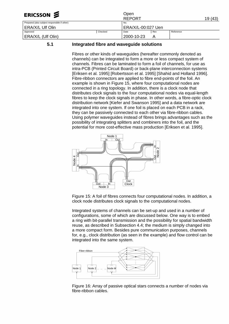
5.1 Integrated fibre and waveguide solutions
Fibres or other kinds of waveguides (hereafter commonly denoted aschannels) can be integrated to form a more or less compact system ofchannels. Fibres can be laminated to form a foil of channels, for use asintra-PCB (Printed Circuit Board) or back-plane interconnection systems[Eriksen et al. 1995] [Robertsson et al. 1995] [Shahid and Holland 1996].Fibre-ribbon connectors are applied to fibre end-points of the foil. Anexample is shown in Figure 15, where four computational nodes areconnected in a ring topology. In addition, there is a clock node thatdistributes clock signals to the four computational nodes via equal-lengthfibres to keep the clock signals in phase. In other words, a fibre-optic clockdistribution network [Kiefer and Swanson 1995] and a data network areintegrated into one system. If one foil is placed on each PCB in a rack,they can be passively connected to each other via fibre-ribbon cables.Using polymer waveguides instead of fibres brings advantages such as thepossibility of integrating splitters and combiners into the foil, and thepotential for more cost-effective mass production [Eriksen et al. 1995].
Node 3
Nod
e 4 N
ode
2
Node 1
ClockOut In
In Out
InO
ut
Out
In
Out
Figure 15: A foil of fibres connects four computational nodes. In addition, aclock node distributes clock signals to the computational nodes.
Integrated systems of channels can be set-up and used in a number ofconfigurations, some of which are discussed below. One way is to embeda ring with bit-parallel transmission and the possibility for spatial bandwidthreuse, as described in Subsection 4.4; the medium is simply changed intoa more compact form. Besides pure communication purposes, channelsfor, e.g., clock distribution (as seen in the example) and flow control can beintegrated into the same system.
Node 1 Node 2 Node M
Fiber-ribbon
Figure 16: Array of passive optical stars connects a number of nodes viafibre-ribbon cables.

OpenREPORT 20 (43)
Prepared (also subject responsible if other) No.
ERA/X/L Ulf Olin ERA/X/L-00:027 UenApproved Checked Date Rev Reference
ERA/X/L (Ulf Olin) 2000-10-23 A
Another way is to follow the proposed use of an array of passive opticalstars to connect processor boards in a multiprocessor system via fibre-ribbon links, for which experiments with 6 x 700 Mbit/s fibre-ribbon linkswere done (see Figure 16) [Parker 1991] [Parker et al. 1992]. Of course,the processor boards can be exchanged with, e.g., transceiver cardsand/or switch cards. As indicated above, such a configuration can beintegrated by the use of polymer waveguides. The power budget can,however, be a limiting factor to the number of nodes and/or the distance.Advantages are simple hardware owing to bit-parallel transmission (likeother fibre-ribbon solutions) and the broadcast nature, but the star arraycan become a bottleneck as in all bus-like systems. In a similar system,the star array is exchanged by a chip (with optoelectronics) that has oneincoming ribbon from each node and one output ribbon [Lukowicz et al.1998]. The output ribbon is coupled to an array of 1 × N couplers so thateach node has a ribbon connected to its receiver. The chip couples theincoming traffic together in a way that simulates a bus. At contention, thechip can temporarily store packets.
Electronic crossbars can be distributed on the PCBs and/or placed on aspecial switch PCB in a back-plane system, and be connected byintegrated parallel channels.
Other similar systems include the integration of fibres into a PCB for thepurpose of clock distribution [Li et al. 1998]. Distribution to up to 128 nodeswas demonstrated. The fibres are laminated on one side of the PCB, whileintegrated circuits are placed on the reversed side. The end section ofeach fibre is bent 90 degrees to lead the light through a so called via holeto the reversed side of the PCB.
5.2 Planar free space optics
By placing electronic chips (including optoelectronic devices) and opticalelements on a substrate where light beams can travel, we get a planar freespace system (Figure 17) [Jahns 1994] [Jahns 1998] [Sinzinger 1998].Electronic chips are placed in a two-dimensional plane, while light beamstravel in a three-dimensional space. In this way, optical systems can beintegrated monolithically, which brings compact, stable and potentiallyinexpensive systems [Jahns 1998]. By using, e.g., Spatial Light Modulatorsto dynamically direct the optical beams, a flexible interconnection networkcan be obtained. Using only fixed interconnection patterns and electronicswitching can, however, give shorter switch times. A planar free spaceoptical crossbar switch has been reported [Reinhorn et al. 1999].

OpenREPORT 21 (43)
Prepared (also subject responsible if other) No.
ERA/X/L Ulf Olin ERA/X/L-00:027 UenApproved Checked Date Rev Reference
ERA/X/L (Ulf Olin) 2000-10-23 A
Figure 17: Example of a planar free space system. The direction of thebeam is steered by the optical element on the way between two chips.
5.3 Free space optical backplanes
Several different optical backplanes have been proposed, three of whichare discussed below. As shown in Figure 18a, using planar free spaceoptics is one means of transporting optical signals between PCBs.Holographic gratings can be used to insert and extract the optical signalsto/from the waveguide, which may be a glass substrate [Zhao et al. 1995].Several beams or bus lines can be used, i.e., each arrow in the figurerepresents several parallel beams [Zhao et al.1996].
(a) (b)
(c)
Figure 18: Optical backplane configurations: (a) with planar free spaceoptics, (b) with smart pixel arrays, and (c) with a mirror.

OpenREPORT 22 (43)
Prepared (also subject responsible if other) No.
ERA/X/L Ulf Olin ERA/X/L-00:027 UenApproved Checked Date Rev Reference
ERA/X/L (Ulf Olin) 2000-10-23 A
In the system shown in Figure 18b, two-dimensional arrays of opticalbeams (typically 10 000) link neighbouring PCBs together in a point-to-point fashion [Szymanski 1995] [Hinton and Szymanski 1995]. Smart pixelarrays then act as intelligent routers that can, e.g., bypass data or performdata extraction operations where some data pass to the local PCB andsome data are retransmitted to the next PCB [Supmonchai and Szymanski1998]. Each smart pixel array can typically contain 1 000 smart pixelsarranged in a two-dimensional array, where each pixel has a receiver, atransmitter, and a simple processing unit. One way of configuring thesystem is to connect the smart pixel arrays in a ring, where the ring can bereconfigured to embed other topologies [Szymanski and Hinton 1995][Szymanski and Supmonchai 1996].
The configuration shown in Figure 18c is similar to the optical backplanebased on planar free space interconnects. The difference is thereplacement of the waveguide by a mirror [Hirabayashi et al. 1998]. Anoptical beam leaving a transmitter is simply bounced once on the mirrorbefore it arrives at the receiver. A regeneration of the optical signal (multi-hop) might be needed on the way from the source to the final destination.
Of the three types of optical backplanes discussed, the one with smartpixel arrays seems to be the most powerful. On the other hand, a simplepassive optical backplane may have other advantages. Other opticalbackplanes have been proposed, e.g., a bus where optical signals canpass through transparent photo detectors or be modulated by spatial lightmodulators [Hamanaka 1991].
6 Optical and optoelectronic switch-fabrics
In this section, optical and optoelectronic switch-fabrics are introduced.First, in Subsection 6.1, the combination of optical interconnections andelectronic crossbars is treated, while WDM/SDM switches are discussed inSubsection 6.2.
6.1 Optical interconnections and electronic crossbars
Communication systems such as Myrinet [Boden et al. 1995], by whicharbitrary switched topologies can be built using electrical switches, havebeen proposed for parallel computing systems and can be adopted fordata- and telecommunication equipment too. Fibre-ribbons can be used toincrease bandwidth, compared to electrical systems, while still sending inbit-parallel mode. It is possible to have bit rates in the order of 1 Gbit/sover each fibre in the ribbon over tens of meters using standard fibre-ribbons. As noted in Subsection 5.1, foils of fibres or waveguides (e.g.,arranged as ribbons) can be used to interconnect nodes and crossbars onthe PCB and/or back-plane level.

OpenREPORT 23 (43)
Prepared (also subject responsible if other) No.
ERA/X/L Ulf Olin ERA/X/L-00:027 UenApproved Checked Date Rev Reference
ERA/X/L (Ulf Olin) 2000-10-23 A
The switch itself can also be modified to increase performance or packingdensity. A single-chip switch core where fibre-ribbons are coupled directlyto optoelectronic devices on the chip is possible [Szymanski et al. 1998].Attaching 32 incoming and 32 outgoing fibre-ribbons with 800 Mbit/s perfibre translates to an aggregated bandwidth of 204 Gbit/s through theswitch when eight fibres on each link are used for data.
A 16×16 crossbar switch chip, with integrated optoelectronic I/O wasimplemented for switching packets transferred using bit-parallel WDM[Krisnamoorthy et al. 1996]. Each node has two single-mode fibrescoupled to the switch, one for input and one for output.
6.2 WDM/SDM switches
The architecture with optical interconnections and electronic crossbars isflexible and powerful. Optics and optoelectronics can however also beused internally in a switch fabric, i.e., more than just in the I/O interface. Abroad spectrum of solutions has been proposed, and some examples aregiven below.
SDM (Space Division Multiplexing) switches [Goh et al. 1998] [Guilfoyle etal. 1998] [Kato et al. 1998] [Lai et al. 1998] [Moosburger and Petermann1998] [Sawchuk et al. 1987] and WDM switches (consisting of, e.g.,wavelength converters and wavelength selective components) [Pedersenet al. 1998] [Flipse 1998] can be used both as stand-alone switches and asbuilding components in larger switch fabrics [Reif and Yoshida 1994]. Asan example, a Banyan multistage network built of 2 x 2 switch elementshas been described [Chamberlain et al. 1998]. Another multistage networkuses both WDM and SDM switches but in different stages [Kawai et al.1995]. A multistage network can also be implemented using chips withprocessing elements placed on a two-dimensional plane [Christensen andHaney 1997]. The processors then communicate with each other by amirror that bounces back the beam to the plane but to another processor.Switching is made on the chips while each pass between two switchstages corresponds to a bounce on the mirror.
A multistage switch incorporating both electrical and optical switching, butin different stages, has also been reported [Duan and Wilmsen 1998].Some work has focused on the communication between stages, e.g.,perfect shuffle with lenses and prisms [Lohmann et al. 1986]. Switch timesfor SDM switches in the order of 1 ns have been reported [Kato et al.1998], while some SDM switches have switch times in the order of 1 ms[Tajima et al. 1998]. A switch can be placed on a dedicated board in acabinet and be connected to processor boards (or, e.g., line cards) viafibres or via an optical backplane [Maeno et al. 1997].

OpenREPORT 24 (43)
Prepared (also subject responsible if other) No.
ERA/X/L Ulf Olin ERA/X/L-00:027 UenApproved Checked Date Rev Reference
ERA/X/L (Ulf Olin) 2000-10-23 A
A system that implements a distributed crossbar, or a fully connectedsystem, connecting N nodes with only passive optics between thetransmitters and receivers has been demonstrated [Li et al. 1998B]. Alloptical channels turned on from a transmitter's two-dimensional √N × √NVCSEL array are inserted into a fibre image guide. The fibre image guidesfrom all transmitters end at a central free space system with lenses. Thelenses are arranged in such a way that the light from each VCSEL pixel ina VCSEL array is focused on a single spot together with the correspondingpixels in all other arrays. This gives N spots where each is focused into asingle fibre leading to a receiver. Hence, selecting a pixel in a VCSELarray to be turned on corresponds to addressing a destination node.
Wavelength converters are important components in many WDM switches.A way of building fast wavelength converters is to first have conversion tothe electrical domain and then back to the optical domain but on anotherwavelength. However, this is not a valid solution if an all-optical switch isdesired.
Lately, a lot of focus has been paid on using MEMS(microelectromechanical systems) technology to build all-optical SDMswitches. As reported in [Lin 1999], an array of electrically controlledmirrors can be used to build an 8×8 OXC. Lucent Technologies hasalready announced 256×256 OXCs to be released on the market [Kenward2000]. Due to the relatively low loss possible in MEMS switches,multistage MEMS switches are also possible. In this way, rather largeoptically transparent switches can be built. In addition to pure SDMswitches, the MEMS technology can be used in equipment for wavelengthrouting networks (wavelength routers), e.g., consisting of wavelengthsplitters, a MEMS SDM switch, and wavelength combiners. Moreinformation on all-optical switching is found in [Pattavina et al. 2000].
7 Commercial system implementations
In this section three products are described where optical interconnecttechnology is used. The exact backplane technology is not stated in thecompanies’ material. The fourth section deals with InfiniBand, which is anindustry association to promote a common interconnect standard forcomputer-related hardware.
7.1 Sycamore
The Sycamore SN 16000 is an optical switching platform that provides atransition of the optical network from a ring-based architecture to a mesh-based network topology. According to Sycamore, the SN 16000 deliversautomated provisioning, routing, and restoration of lightpaths.
VCSEL (Vertical Cavity Surface Emitting Laser) technology is used tointerconnect the switch fabric shelf with the port card shelf as well as tointerconnect card to card within a shelf. According to Sycamore, thisoptical interconnect technology system enables scalability to large switchmatrix sizes, while maintaining a high port density.

OpenREPORT 25 (43)
Prepared (also subject responsible if other) No.
ERA/X/L Ulf Olin ERA/X/L-00:027 UenApproved Checked Date Rev Reference
ERA/X/L (Ulf Olin) 2000-10-23 A
7.2 Pluris
The Pluris terabit network router architecture uses a distributed switchingfabric and an n-dimensional fibre optic interconnect structure to providescalability in terms of switching capacity, line capacity, port density and linerate forwarding. The system supports thousands of IP enabled OC-12, OC-48 and OC-192 interfaces by combining up to 1920 line cards within asingle system.
7.3 Sirocco Systems
The Sirocco Zephyr Optical Access Device is a network element, designedto aggregate services onto the optical network. There are two Zephyrmodels: the Zephyr Z-48 which provides aggregation up to OC-48/STM-16and includes an integral optical backplane for support of multiplewavelengths, and the Zephyr Z-12 offering aggregation up to OC-12/STM-4 for entry-level applications. Zephyrs are designed for deployment in theMetro or Access layer of the network and will typically be located in centraloffices and multi-tenant buildings.
7.4 InfiniBand Trade Association
Seven computing companies, Compaq, Dell, Hewlett-Packard, IBM, Intel,Microsoft and Sun Microsystems have joined together to develop a newcommon I/O specification to deliver a channel based switched fabrictechnology. This issue is addressed through an independent industry bodycalled the InfiniBand Trade Association. The specification will support bothcopper and fibre implementations and the performance range will bescalable from 500MB/s to 6GB/s per link.
8 Conclusions
Reviewed interconnection architectures are summarised in Table 2 withremarks on their suitability in data- and telecommunication equipment fromdifferent aspects. Switch time is marked as slow (ms), medium (sub-microsecond), or fast (ns) in the table depending on the suitability ofadoption in OXCs, packet switches with burst switching, or true packetswitches, respectively.
Optical transparency is valuable to get protocol-independent OXCs. TheMEMS technology is promising for such systems, at least as long as therequirements on switch times are moderate. Multistage networks usingMEMS technology can be especially good alternatives because of theirscalability. All-optical packet switches, however, will probably not bemature technology in the near future. Also, one must think of the flexibilityand power of electronic switches, and of processors to control theswitches.

OpenREPORT 26 (43)
Prepared (also subject responsible if other) No.
ERA/X/L Ulf Olin ERA/X/L-00:027 UenApproved Checked Date Rev Reference
ERA/X/L (Ulf Olin) 2000-10-23 A
Scalability is desired to be able to build equipment with many in-/outputports. We state the scalability as poor if only tens of ports is realistic,medium for hundred to a few hundred ports, and good for thousand portsor more. Different multistage networks and free space optical backplaneswith a high density of optical channels seems to be good candidates froma scalability point of view. When building smaller systems instead, e.g., theWDM star distributed crossbar with its passive optical star can be a goodand simple alternative.
If an interconnection network implements a true crossbar it is non-blocking(e.g., WDM star distributed crossbar), while it is topology dependent formany of the reviewed architectures whether they are blocking or non-blocking. It should, however, be noticed that the fibre-ribbon pipeline ringnetwork is blocking. On the other hand, the increasingly goodprice/performance ratio for fibre-ribbon links indicates a great successpotential for interconnection systems using fibre-ribbon links.
Switchtime
Opticaltrans-
parencyScala-bility
Blocking Notes
WDM star distributed crossbar fast internally poor tomedium
non-blocking
Slow switching relaxes component’stuning time requirements.
WDM ring fast internally poor non-blocking
Slow switching relaxes component’stuning time requirements.
Fibre-ribbon pipeline ring fast no poor blocking Can be compared with a bus but withspatial bandwidth reuse
Free space optical backplanes varies a lot internallyfor somesystems
varies alot
varies alot
Scalable if many I/O channels on onecard. Switching and line cards can bemixed.
Nonblocking MEMS system slow yes medium(or better)
non
Multistage MEMS system slow yes good topologydependent
Scalable optically transparent forsystems with relaxed switching timerequirements
WDM/SDM switches slow(or better)
(yes) varies alot
topologydependent
For optical transparency, only all-optical wavelength conversion isallowed.
Optical interconnections andelectronic crossbar
fast no poor tomedium
non-blocking
Many optoelectronic I/O channels canbe integrated on a switchingchip/module
Planar free space optics fast if noSLMs
no good topologydependent
Chips are only placed in twodimensions. Promising in terms ofassembly.
Table 2: Summarising evaluation of reviewed interconnection architectures.

OpenREPORT 27 (43)
Prepared (also subject responsible if other) No.
ERA/X/L Ulf Olin ERA/X/L-00:027 UenApproved Checked Date Rev Reference
ERA/X/L (Ulf Olin) 2000-10-23 A
Having optics inside a switch gives the same flexibility as electroniccrossbars, but it might be possible to build larger switch fabrics with hightransmission capacities using optics. The suitability of the different freespace systems depends a great deal on the more detailed configurationsof the systems. For example, planar free space systems can be arrangedin arbitrary topologies.
Integrated fibre and waveguide solutions make the building of compactsystems possible, especially for networks such as those using fibre-ribbons. The same reasoning about compactness can be argued for freespace systems. Optical backplanes may earn their success from thesimilarities with current rack-based systems, while future planar free-spacesystems might give the possibility to integrate optics and electronics in acompact way, easy to assemble.
9 References
[Acampora and Karol 1989] A. S. Acampora and M. J. Karol, "An overviewof lightwave packet networks," IEEE Network, pp. 29-41, Jan. 1989.
[Aronson et al. 1998] L. B. Aronson, B. E. Lemoff, L. A. Buckman, and D.W. Dolfi, “ Low-cost multimode WDM for local area networks up to 10Gb/s,” IEEE Photonics Technology Letters," vol. 10, no. 10, pp. 1489-1491, Oct. 1998.
[Arvind et al. 1991] K. Arvind, K. Ramamritham, and J. A. Stankovic, “Alocal area network architecture for communication in distributed real-timesystems,” Journal of Real-Time Systems, vol. 3, no. 2, pp. 115-147, May1991.
[Bergman et al. 1998] L. Bergman, J. Morookian, and C. Yeh, “An all-optical long-distance multi-Gbytes/s bit-parallel WDM single-fibre link,”Journal of Lightwave Technology, vol. 16, no. 9, pp. 1577-1582, Sept.1998.
[Bergman et al. 1998B] L. A. Bergman, C. Yeh, and J. Morookian,”Towards the realization of multi-km × Gbyte/sec bit-parallel WDM singlefibre computer links,” Proc. 5th International Conference on MassivelyParallel Processing using Optical Interconnections (MPPOI’98), LasVegas, NV, USA, June 15-17, 1998, pp. 218-223.
[Blumenthal et al. 1999] D. J. Blumenthal, A. Carena, L. Rau, V. Curri, S.Humphries, "WDM optical IP tag switching with packet-rate wavelengthconversion and subcarrier multiplexed addressing," Optical FibreCommunication Conference, OFC’99, pp. 162-164, 1999.
[Boden et al. 1995] N. J. Boden, D. Cohen, R. E. Felderman, A. E.Kulawik, C. L. Seitz, J. N. Seizovic, and W.-K. Su, "Myrinet: a gigabit-per-second local area network," IEEE Micro, vol. 15, no. 1, pp. 29-36, Feb.1995.

OpenREPORT 28 (43)
Prepared (also subject responsible if other) No.
ERA/X/L Ulf Olin ERA/X/L-00:027 UenApproved Checked Date Rev Reference
ERA/X/L (Ulf Olin) 2000-10-23 A
[Brackett 1990] C. A. Brackett, "Dense wavelength division multiplexingnetworks: principles and applications," IEEE Journal on Selected Areas inCommunications, vol. 8, no. 6, pp. 948-964, Aug. 1990.
[Brackett 1991] C. A. Brackett, “On the capacity of multiwavelength optical-star packet switches,” IEEE LTS, pp. 33-37, May 1991.
[Brackett 1996] C. A. Brackett, “Foreword: Is there an emerging consensuson WDM networking?,” Journal of Lightwave Technology, vol. 14, no. 6,pp. 936-941, June 1996.
[Buckman et al. 1998] L. Buckman, A. Yuen, K. Giboney, P. Rosenberg, J.Straznicky, K. Wu, and D. Dolfi, "Parallel optical interconnects," Proc. HotInterconnects VI, Stanford, CA, USA, Aug. 13-15, 1998, pp. 137-143.
[Bursky 1994] D. Bursky, "Parallel optical links move data at 3 Gbits/s,"Electronic Design, vol. 42, no. 24, pp. 79-82, Nov. 21, 1994.
[Callegati et al. 1999] F. Callegati, A.C. Cankaya, Y. Xiong, and M.Vandenhoute, “Design issues of optical IP routers for Internet backboneapplications,” IEEE Communications Magazine, vol. 37, no. 12, pp. 124-128, Dec. 1999.
[Chamberlain et al. 1998] R. D. Chamberlain, M. A. Franklin, R. B.Krchnavek, and B. H. Baysal, ”Design of an optically-interconnectedmultiprocessor,” Proc. 5th International Conference on Massively ParallelProcessing using Optical Interconnections (MPPOI’98), Las Vegas, NV,USA, June 15-17, 1998, pp. 114-122.
[Cheung 1990] K.-W. Cheung, "Acoustooptic tunable filters in narrowbandWDM networks: system issues and network applications," IEEE Journal onSelected Areas in Communications, vol. 8, no. 6, pp. 1015-1025, Aug.1990.
[Chiaroni et al. 1998] D. Chiaroni, B. Lavigne, L. Hamon, A. Jourdan, F.Dorgeuille, C. Janz, E. Grard, M. Renaud, R. Bauknecht, C. Graf, H.PSchneibel, and H. Melchior, "Experimental validation of an all-opticalnetwork based on 160 Gbit/s throughput packet switching nodes," Proc.24th European Conference on Optical Communication, Madrid, Spain,Sept. 20-24, 1998, vol. 1, pp. 573-574.
[Christensen and Haney 1997] M. P. Christensen and M. W. Haney, ”Two-bounce free-space arbitrary interconnection architecture,” Proc. MassivelyParallel Processing using Optical Interconnections (MPPOI’97), Montreal,Canada, June 22-24, 1997, pp. 61-67.
[Coldren et al. 1998] L. A. Coldren, E. R. Hegblom, Y. A. Akulova, J. Ko, E.M. Strzelecka, and S. Y. Hu, ”Vertical-cavity lasers for parallel opticalinterconnects,” Proc. 5th International Conference on Massively ParallelProcessing using Optical Interconnections (MPPOI’98), Las Vegas, NV,USA, June 15-17, 1998, pp. 2-10.

OpenREPORT 29 (43)
Prepared (also subject responsible if other) No.
ERA/X/L Ulf Olin ERA/X/L-00:027 UenApproved Checked Date Rev Reference
ERA/X/L (Ulf Olin) 2000-10-23 A
[Duan and Wilmsen 1998] C. Duan and C. W. Wilmsen, "OptoelectronicATM switch using VCSEL and smart detector arrays," Proc. Optics inComputing (OC'98), Brugge, Belgium, June 17-20, 1998, pp. 103-106.
[Eng 1988] K. Y. Eng, "A photonic knockout switch for high-speed packetnetworks," IEEE Journal on Selected Areas in Communications, vol. 6, no.7, pp. 1107-1116, Aug. 1988.
[Engebretsen et al. 1996] D. R. Engebretsen, D. M. Kuchta, R. C. Booth, J.D. Crow, and W. G. Nation, "Parallel fibre-optic SCI links," IEEE Micro, vol.16, no. 1, pp. 20-26, Feb. 1996.
[Eriksen et al. 1995] P. Eriksen, K. Gustafsson, M. Niburg, G. Palmskog,M. Robertsson, and K. Åkermark, "The Apollo demonstrator − new low-cost technologies for optical interconnects," Ericsson Review, vol. 72, no.2, 1995.
[Fibre Systems 1998] "Parallel optics can feed the clamour for speed,"Fibre Systems, vol. 2, no. 4, pp. 27-28, May 1998.
[Flipse 1998] R. Flipse, "Optical switches ease bandwidth crunch,"EuroPhotonics, vol. 3, no. 5, pp. 44-45, Aug./Sept. 1998.
[Fujimoto et al. 1998] N. Fujimoto, A. Ishizuka, H. Rokugawa, and K. Mori,“Skew-free parallel optical transmission systems,” Journal of LightwaveTechnology, vol. 16, no. 10, pp. 1822-1831, Oct. 1998.
[Goh et al. 1998] T. Goh, M. Yasu, K. Hattori, A. Himeno, M. Okuno, andY. Ohmori, “Low-loss and high-extinction-ratio silica-based strictlynonblocking 16 × 16 thermooptic matrix switch,” IEEE PhotonicsTechnology Letters," vol. 10, no. 6, pp. 810-812, June 1998.
[Goke and Lipovski 1973] L. R. Goke and G. J. Lipovski, "Banyan networksfor partitioning multiprocessor systems," Proc. 1st International Symposiaon Computer Architecture (ISCA'73), 1973.
[Guilfoyle et al. 1998] P. S. Guilfoyle, J. M. Hessenbruch, and R. V. Stone,“Free-space interconnects for high-performance optoelectronic switching,”Computer, vol. 31, no. 2, pp. 69-75, Feb. 1998.
[Hahn 1995] K. H. Hahn, "POLO – Parallel optical links for gigabyte/s datacommunications," Proc. LEOS’95, San Francisco, CA, USA, Oct. 30 –Nov. 2, 1995, vol. 1, pp. 228-229.
[Hahn 1995B] K. H. Hahn, "POLO − parallel optical links for Gigabyte datacommunications," Proc. of the 45th Electronics Components andTechnology Conference (ECTC’95), pp. 368-375, 1995.
[Hahn et al. 1995] K. H. Hahn et al., "POLO: parallel optical links forworkstation clusters and switching systems," Conference on Optical FibreCommunication, OFC’95 Technical Digest, pp. 112-112, 1995.

OpenREPORT 30 (43)
Prepared (also subject responsible if other) No.
ERA/X/L Ulf Olin ERA/X/L-00:027 UenApproved Checked Date Rev Reference
ERA/X/L (Ulf Olin) 2000-10-23 A
[Hahn et al. 1996] K. H. Hahn, K. S. Giboney, R. E. Wilson, J. Straznicky,E. G. Wong, M. R. Tan, R. T. Kaneshiro, D. W. Dolfi, E. H. Mueller, A. E.Plotts, D. D. Murray, J. E. Marchegiano, B. L. Booth, B. J. Sano, B.Madhavan, B. Raghavan, A. F. J. Levi, "Gigabyte/s data communicationswith the polo parallel optical link," Proc. of the 46th ElectronicsComponents and Technology Conference (ECTC’96), May 1996.
[Hamanaka 1991] K. Hamanaka, “Otical bus interconnection system usingselfloc lenses,” Optics Letters, vol. 16, no. 6, pp. 1222-1224, Aug. 15,1991.
[Hartman et al. 1990] D. H. Hartman, L. A. Reith, S. F. Habiby, G. R. Lalk,B. L. Booth, J. E. Marchegiano, and J. L. Hohman, "Power economy usingpoint-to-point optical interconnects," in Microelectronic Interconnects andPackages: System and Process Integration, Proc. SPIE vol. 1390, S. K.Tewksbury and J. R. Carruthers, Eds., pp. 368-376, 1990.
[Hinton and Szymanski 1995] H. S. Hinton and T. H. Szymanski,”Intelligent optical backplanes,” Proc. 2nd International Conference onMassively Parallel Processing using Optical Interconnections (MPPOI’95),San Antonio, TX, USA, Oct 23-24, 1995, pp. 133-143.
[Hirabayashi et al. 1998] K. Hirabayashi, T. Yamamoto, and S. Hino,“Optical backplane with free-space optical interconnections using tunablebeam deflectors and a mirror for bookshelf-assembled terabit per secondclass asynchronous transfer mode switch,” Optical Engineering, vol. 37,no. 4, pp. 1332-1342, Apr. 1998.
[Honeywell] Honeywell, 850 nm VCSEL products, OptoelectronicsReliability Study.
[Irshid and Kavehrad 1992] M. I. Irshid and M. Kavehrad, “A fullytransparent fibre-optic ring architecture for WDM networks,” Journal ofLightwave Technology, vol. 10, no. 1, pp. 101-108, Jan. 1992.
[Jahns 1994] J. Jahns, ”Planar packaging of free-space opticalinterconnects,” Proceedings of the IEEE, vol. 82, no. 11, pp. 1623-1631,Nov. 1994.
[Jahns 1998] J. Jahns, ”Integrated free-space optical interconnects forchip-to-chip communications,” Proc. 5th International Conference onMassively Parallel Processing using Optical Interconnections (MPPOI’98),Las Vegas, NV, USA, June 15-17, 1998, pp. 20-23.
[Jason and Arvidsson 2000] P. Johan Jason and C. Bertil Arvidsson,“Aspects of skew in modern 12-fibre ribbon manufacturing”. Conferencecontribution from ECA to be presented at cable conference in Stuttgartsummer 2000.

OpenREPORT 31 (43)
Prepared (also subject responsible if other) No.
ERA/X/L Ulf Olin ERA/X/L-00:027 UenApproved Checked Date Rev Reference
ERA/X/L (Ulf Olin) 2000-10-23 A
[Jeong and Goodman 1996] G. Jeong and J. W. Goodman, “Long-distance parallel data link using WDM transmission with bit-skewcompensation,” Journal of Lightwave Technology, vol. 14, no. 5, pp. 655-660, May 1996.
[Jiang et al. 1995] C.-L. Jiang, D. J. Brown, E. H. Mueller, A. E. Plotts, E.Cornejo, S. O'Neill, A. J. Heiney, and B. H. Reysen, "LED based paralleloptical links," Proc. LEOS’95, San Francisco, CA, USA, Oct. 30 – Nov. 2,1995, vol. 1, pp. 224-225.
[Jiang et al. 1998] W. Jiang, L. J. Norton, P. Kiely, D. B. Schwartz, B.Gable, M. Lebby, and G. Raskin, “Vertical cavity surface emitting laser-based parallel optical data link,” Optical Engineering, vol. 37, no. 12, pp.3113-3118, Dec. 1998.
[Jonsson 1998] M. Jonsson, “Control-channel based fibre-ribbon pipelinering network," Proc. Massively Parallel Processing using OpticalInterconnections (MPPOI’98), Las Vegas, NV, USA, June 15-17, 1998, pp.158-165.
[Jonsson 1998B] M. Jonsson, “Two fibre-ribbon ring networks for paralleland distributed computing systems,” Optical Engineering, vol. 37, no. 12,pp. 3196-3204, Dec. 1998.
[Jonsson and Svensson 1997] M. Jonsson and B. Svensson, “On inter-cluster communication in a time-deterministic WDM star network,” toappear in Proc. 2nd Workshop on Optics and Computer Science (WOCS),Geneva, Switzerland, Apr. 1, 1997.
[Jonsson et al. 1996] M. Jonsson, A. Åhlander, M. Taveniku, and B.Svensson, “Time-deterministic WDM star network for massively parallelcomputing in radar systems,” Proc. Massively Parallel Processing usingOptical Interconnections (MPPOI’96), Maui, HI, USA, Oct. 27-29, 1996, pp.85-93.
[Jonsson et al. 1997] M. Jonsson, K. Börjesson, and M. Legardt, “Dynamictime-deterministic traffic in a fibre-optic WDM star network,” Proc. 9thEuromicro Workshop on Real Time Systems, Toledo, Spain, June 11-13,1997, pp. 25-33.
[Jonsson et al. 1997B] M. Jonsson, B. Svensson, M. Taveniku, and A.Åhlander, “Fibre-ribbon pipeline ring network for high-performancedistributed computing systems,” Proc. International Symposium on ParallelArchitectures, Algorithms and Networks (I-SPAN’97), Taipei, Taiwan, Dec.18-20, 1997, pp. 138-143.
[Kanjamala and Levi 1995] A. P. Kanjamala and A. F. J. Levi, "Sub-picosecond skew in multimode fibre ribbon for synchronous datatransmission," Electronics Letters, vol. 31, pp. 1376-1377, 1995.

OpenREPORT 32 (43)
Prepared (also subject responsible if other) No.
ERA/X/L Ulf Olin ERA/X/L-00:027 UenApproved Checked Date Rev Reference
ERA/X/L (Ulf Olin) 2000-10-23 A
[Karstensen 1995] H. Karstensen, "Parallel optical links – PAROLI, a lowcost 12-channel optical interconnection," Proc. LEOS’95, San Francisco,CA, USA, Oct. 30 – Nov. 2, 1995, vol. 1, pp. 226-227.
[Karstensen et al. 1995] H. Karstensen, C. Hanke, M. Honsberg, J.-R.Kropp, J. Wieland, M. Blaser, P. Weger, and J. Popp, “Parallel opticalinterconnection for uncoded data transmission with 1 Gb/s-per-channelcapacity, high dynamic range, and low power consumption,” Journal ofLightwave Technology, vol. 13, no. 6, pp. 1017-1030, June 1995.
[Karstensen et al. 1998] H. Karstensen, J. Wieland, R. Dal'Ara, and M.Blaser, “Parallel optical link for multichannel interconnections at gigabitrate,” Optical Engineering, vol. 37, no. 12, pp. 3119-3123, Dec. 1998.
[Kasahara 1998] K. Kasahara, "Optical interconnects speed up networks,"Photonics Spectra, vol. 32, no. 2, pp. 127-128, 1998.
[Kato et al. 1998] T. Kato, J. Sasaki, T. Shimoda, H. Hatakeyama, T.Tamanuki, M. Yamaguchi, M. Kitamura, and M. Itoh, "10 Gb/s photonic cellswitching with hybrid 4×4 optical matrix switch module on silica basedplanar waveguide platform," Optical Fibre Communication Conference,OFC’98 Technical Digest, San Jose, CA, USA, Feb. 22-27, 1998, pp. 437-440.
[Kawai et al. 1995] S. Kawai, H. Kurita, and K. Kubota, ”Design of electro-photonic computer-networks with non-blocking and self-routing functions,"Optical Computing, vol. 10, 1995 OSA Technical Digest Series, Salt LakeCity, Utah, Mar. 13-16, 1995, pp. 263-265.
[Kenward 2000] M. Kenward, "Mirror magic ushers in the all.opticalnetwork," Fibre Systems, pp. 37-39, May 2000.
[Kiefer and Swanson 1995] D. R. Kiefer and V. W. Swanson,”Implementation of optical clock distribution in a supercomputer," OpticalComputing, vol. 10, 1995 OSA Technical Digest Series, Salt Lake City,Utah, Mar. 13-16, 1995, pp. 260-262.
[Kobrinski et al. 1988] H. Kobrinski, M. P. Vecchi, E. L. Goldstein, and R.M. Bulley, "Wavelength selection with nanosecond switching times usingdistributed-feedback laser amplifiers," Electronics Letters, vol. 24, no. 15,pp. 969-971, July 21, 1988.
[Kou 1999] K. Y. Kou, “Realization of large-capacity ATM switches,” IEEECommunications Magazine, vol. 37, no. 12, pp. 120-123, Dec. 1999.
[Krisnamoorthy et al. 1996] A. V. Krisnamoorthy, J. E. Ford, K. W. Goosen,J. A. Walker, B. Tseng, S. P. Hui, J. E. Cunningham, W. Y. Jan, T. K.Woodward, M. C. Nuss, R. G. Rozier, F. E. Kiamilev, and D. A. B. Miller,”The AMOEBA chip: an optoelectronic switch for multiprocessornetworking using dense-WDM,” Proc. 3rd International Conference onMassively Parallel Processing using Optical Interconnections (MPPOI’96),Maui, HI, USA, Oct. 27-29, 1996, pp. 94-100.

OpenREPORT 33 (43)
Prepared (also subject responsible if other) No.
ERA/X/L Ulf Olin ERA/X/L-00:027 UenApproved Checked Date Rev Reference
ERA/X/L (Ulf Olin) 2000-10-23 A
[Kuchta et al. 1998] D. M. Kuchta, J. Crow, P. Pepeljugoski, K. Stawiasz, J.Trewhella, D. Booth, W. Nation, C. DeCusatis, and A. Muszynski, ”Lowcost 10 gigabit/s optical interconnects for parallel processing,” Proc. 5thInternational Conference on Massively Parallel Processing using OpticalInterconnections (MPPOI’98), Las Vegas, NV, USA, June 15-17, 1998, pp.210-215.
[Kurokawa et al. 1998] T. Kurokawa, S. Matso, T. Nakahara, K. Tateno, Y.Ohiso, A. Wakatsuki, and H. Tsuda, ”Design approaches for VCSEL’s andVCSEL-based smart pixels toward parallel optoelectronic processingsystems," Applied Optics, vol. 37, no. 2, pp. 194-204, Jan. 10, 1998.
[Lai et al. 1998] Q. Lai, W. Hunziker, and H. Melchior, “Low-power compact2 × 2 thermooptic silica-on-silicon waveguide switch with fast response,”IEEE Photonics Technology Letters," vol. 10, no. 5, pp. 681-683, May1998.
[Lei et al. 1999] C. Lei et al, “Manufacturing of oxide VCSEL at Hewlett-Packard”, 1999 Digest of the LEOS Summer Topical Meetings:Nanostructures and Quantum Systems (IEEE, Piscataway, NJ, USA,1999) p. III.11-12.
[Li et al. 1995] Y. Li, H. Kosaka, T. Wang, S. Kawai, and K. Kasahara,”Applications of fibre image guides to bit-parallel optical interconnections,"Optical Computing, vol. 10, 1995 OSA Technical Digest Series, Salt LakeCity, Utah, Mar. 13-16, 1995, pp. 286-288.
[Li et al. 1998] Y. Li, J. Popelek, J.-K. Rhee, L. J. Wang, T. Wang, and K.Shum, ”Demonstration of fibre-based board-level optical clockdistributions,” Proc. 5th International Conference on Massively ParallelProcessing using Optical Interconnections (MPPOI’98), Las Vegas, NV,USA, June 15-17, 1998, pp. 224-228.
[Li et al. 1998B] Y. Li, T. Wang, and S. Kawai, ”Distributed crossbarinterconnects with vertical-cavity surface-emitting laser-angle multiplexingand fibre image guides," Applied Optics, vol. 37, no. 2, pp. 254-263, Jan.10, 1998.
[Lin 1999] L. Y. Lin, " Free-space micromachined optical-switchingtechnologies and architectures," Optical Fibre Communication Conference,OFC’99, vol. 2, pp. 154-156, 1999.
[Loeb and Stilwell 1988] M. L. Loeb and G. R. Stilwell, "High-speed datatransmission on an optical fibre using a byte-wide WDM system," Journalof Lightwave Technology, vol. 6, no. 8, pp. 1306-1311, Aug. 1988.
[Loeb and Stilwell 1990] M. L. Loeb and G. R. Stilwell, "An algorithm forbit-skew correction in byte-wide WDM optical fibre systems," Journal ofLightwave Technology, vol. 8, no. 2, pp. 239-242, Aug. 1988.

OpenREPORT 34 (43)
Prepared (also subject responsible if other) No.
ERA/X/L Ulf Olin ERA/X/L-00:027 UenApproved Checked Date Rev Reference
ERA/X/L (Ulf Olin) 2000-10-23 A
[Lohmann et al. 1986] A. W. Lohmann, W. Stork, and G. Stucke, ”Opticalperfect shuffle," Applied Optics, vol. 25, no. 10, pp. 1530-1531, May 15,1986.
[Lukowicz et al. 1998] P. Lukowicz, S. Sinzinger, K. Dunkel, and H.-D.Bauer, "Design of an opto-electronic VLSI/parallel fibre bus," Proc. Opticsin Computing (OC'98), Brugge, Belgium, June 17-20, 1998, pp. 289-292.
[Maeno et al. 1997] Y. Maeno, A. Tajima, Y. Suemura, and N. Henmi, ”8.5Gbit/s/port synchronous optical packet-switch,” Proc. Massively ParallelProcessing using Optical Interconnections (MPPOI’97), Montreal, Canada,June 22-24, 1997, pp. 114-119.
[Mitel] Mitel Semiconductor, MFT62340-J, Parallel Fibre Transmitter(February 2000)
[Montgomery 2000] J.D. Montgomery, “Optical backplanes show dynamicgrowth potential”, Lightwave, vol. 17 (March 2000).
[Moosburger and Petermann 1998] R. Moosburger and K. Petermann, “4× 4 digital optical matrix switch using polymeric oversized rib waveguides,”IEEE Photonics Technology Letters," vol. 10, no. 5, pp. 684-686, May1998.
[Mukherjee 1992] B. Mukherjee, "WDM-based local lightwave networkspart I: single-hop systems," IEEE Network, pp. 12-27, May 1992.
[Mukherjee 1992B] B. Mukherjee, "WDM-based local lightwave networkspart II: multihop systems," IEEE Network, pp. 20-32, July 1992.
[Nagarajan et al. 1998] R. Nagarajan, W. Sha, B. Li, and R. Craig,“Gigabyte/s parallel fibre-optic links based on edge emitting laser diodearrays,” Journal of Lightwave Technology, vol. 16, no. 5, pp. 778-787, Maj1998.
[Nassehi et al. 1985] M. M. Nassehi, F. A. Tobagi, and M. E. Marhic, "Fibreoptic configurations for local area networks," IEEE Journal on SelectedAreas in Communications, vol. 3, no. 6, pp. 941-949, Nov. 1985.
[National] National Semiconductor, DS92LV1021, 16-40 MHz 10 Bit BusLVDS Serializer and Deserializer
[Nishikido et al. 1995] J. Nishikido, S. Fujita, Y. Arai, Y. Akahori, S. Hino,and K. Yamasaki, “Multigigabit multichannel optical interconnection modulefor broadband switching system,” Journal of Lightwave Technology, vol.13, no. 6, pp. 1104-1110, June 1995.
[Nishimura et al. 1997] S. Nishimura, H. Inoue, S. Hanatani, H. Matsuoka,and T. Yokota, “Optical interconnections for the massively parallelcomputer,” IEEE Photonics Technology Letters," vol. 9, no. 7, pp. 1029-1031, July 1997.

OpenREPORT 35 (43)
Prepared (also subject responsible if other) No.
ERA/X/L Ulf Olin ERA/X/L-00:027 UenApproved Checked Date Rev Reference
ERA/X/L (Ulf Olin) 2000-10-23 A
[Nishimura et al. 1998] S. Nishimura, H. Inoue, S. Hanatani, H. Matsuoka,and T. Yokota, “Error-free optical inter-node connection for the massivelyparallel computer,” IEEE Photonics Technology Letters," vol. 10, no. 1, pp.147-149, Jan. 1998.
[Parker 1991] J. W. Parker, “Optical interconnection for advancedprocessor systems: A review of the ESPRIT II OLIVES program,” Journalof Lightwave Technology, vol. 9, no. 12, pp. 1764-1773, Dec. 1991.
[Parker et al. 1992] J. W. Parker, P. J. Ayliffe, T. V. Clapp, M. C. Geear, P.M. Harrison, and R. G. Peall, "Multifibre bus for rack-to-rack interconnectsbased on opto-hybrid transmitter/receiver array pair," Electronics Letters,vol. 28, no. 8, pp. 801-803, April 9, 1992.
[Pattavina et al. 2000] A. Pattavina, M. Martinelli, G. Maier, and P. Boffi,“Techniques and technologies towards all-optical switching,” OpticalNetworks Magazine, vol. 1, no. 2, pp. 75-93, Apr. 2000.
[Peall 1995] R. G. Peall, "Development in multi-channel opticalinterconnects under ESPRIT III SPIBOC," Proc. LEOS’95, San Francisco,CA, USA, Oct. 30 – Nov. 2, 1995, vol. 1, pp. 222-223.
[Pedersen et al. 1998] R. J. S. Pedersen, B. Mikkelsen, B. F. Jørgensen,M. Nissov, K. E. Stubkjaer, K. Wünstel, K. Daub, E. Lach, G. Laube, W.Idler, M. Schilling, P. Doussiere, and F. Pommerau, "WDM cross-connectcascade based on all-optical wavelength converters for routing andwavelength slot interchanging using a reduced number of internalwavelengths," Optical Fibre Communication Conference, OFC’98Technical Digest, San Jose, CA, USA, Feb. 22-27, 1998, pp. 58-59.
[Raghavan et al. 1999] B. Raghavan, Y.-G. Kim, T.-Y. Chuang, B.Madhavan, and A. F. J. Levi, "A Gbyte/s parallel fibre-optic networkinterface for multimedia applications," IEEE Network, vol. 13, no. 1, pp. 20-28, Jan./Feb. 1999.
[Reif and Yoshida 1994] J. H. Reif and A. Yoshida, ”Free space opticalmessage routing for high performance parallel computers,” Proc.Massively Parallel Processing using Optical Interconnections (MPPOI’94),Cancun, Mexico, Apr. 26-27, 1994, pp. 37-44.
[Reinhorn et al. 1999] S. Reinhorn, R. Oron, Y. Amitai, A. A. Friesem, K.Vinokur, and N. Pilossof, “Planar optical dynamic crossbar switch,” OpticalEngineering, vol. 38, no. 8, pp. 1396-1401, Aug. 1999.
[Robertsson et al. 1995] M. Robertsson, K. Engberg, P. Eriksen, H.Hesselbom, M. Niburg, and G. Palmskog, "Optical interconnects inpackaging for telecom applications," Proc. of the 10th EuropeanMicroelectronics Conference, pp. 580-591, 1995.
[Sadot and Elhanany 2000] D. Sadot and I. Elhanany, “Optical switchingspeed requirements for Terabit/second packet over WDM networks,” IEEEPhotonics Technology Letters," vol. 12, no. 4, pp. 440-442, Apr. 2000.

OpenREPORT 36 (43)
Prepared (also subject responsible if other) No.
ERA/X/L Ulf Olin ERA/X/L-00:027 UenApproved Checked Date Rev Reference
ERA/X/L (Ulf Olin) 2000-10-23 A
[Sano and Levi 1998] B. J. Sano and A. F. J. Levi, "Networks for theprofessional campus environment," in Multimedia Technology forApplications. B. Sheu and M. Ismail, Eds., McGraw-Hill, Inc., pp. 413-427,1998, ISBN 0-7803-1174-4.
[Sano et al. 1996] B. Sano, B. Madhavan, and A. F. J. Levi, "8 GbpsCMOS interface for parallel fibre-optic interconnects," Electronics Letters,vol. 32, pp. 2262-2263, 1996.
[Sawchuk et al. 1987] A. A. Sawchuk, B. K. Jenkins, C. S. Raghavendra,and A. Varma, “Optical crossbar networks,” Computer, vol. 20, no. 6, pp.50-60, June 1987.
[Schwartz et al. 1996] D. B. Schwartz, K. Y. Chun, N. Choi, D. Diaz, S.Planer, G. Raskin, and S. G. Shook, ”OPTOBUS I: performance of a 4Gb/s optical interconnect,” Proc. Massively Parallel Processing usingOptical Interconnections (MPPOI’96), Maui, HI, USA, Oct. 27-29, 1996, pp.256-263.
[Shahid and Holland 1996] M. A. Shahid and W. R. Holland, ”Flexibleoptical backplane interconnections,” Proc. 3rd International Conference onMassively Parallel Processing using Optical Interconnections (MPPOI’96),Maui, HI, USA, Oct. 27-29, 1996, pp. 178-185.
[Siala et al. 1994] S. Siala, A. P. Kanjamala, R. N. Nottenburg, and A. F. J.Levi, "Low skew multimode ribbon fibres for parallel opticalcommunication," Electronics Letters, vol. 30, no. 21, pp. 1784-1786, Oct.13, 1994.
[Sinzinger 1998] S. Sinzinger, "Planar optics as the technological platformfor optical interconnects," Proc. Optics in Computing (OC'98), Brugge,Belgium, June 17-20, 1998, pp. 40-43.
[Supmonchai and Szymanski 1998] B. Supmonchai and T. Szymanski,"High speed VLSI concentrators for terabit intelligent optical backplanes,"Proc. Optics in Computing (OC'98), Brugge, Belgium, June 17-20, 1998,pp. 306-310.
[Szymanski 1995] T. H. Szymanski, ”Intelligent optical backplanes,"Optical Computing, vol. 10, 1995 OSA Technical Digest Series, Salt LakeCity, Utah, Mar. 13-16, 1995, pp. 11-13.
[Szymanski and Hinton 1995] T. Szymanski and H. S. Hinton, ”Design of aterabit free-space photonic backplane for parallel computing,” Proc. 2ndInternational Conference on Massively Parallel Processing using OpticalInterconnections (MPPOI’95), San Antonio, TX, USA, Oct 23-24, 1995, pp.16-27.
OpenREPORT 37 (43)
Prepared (also subject responsible if other) No.
ERA/X/L Ulf Olin ERA/X/L-00:027 UenApproved Checked Date Rev Reference
ERA/X/L (Ulf Olin) 2000-10-23 A
[Szymanski and Supmonchai 1996] T. H. Szymanski and B. Supmonchai,”Reconfigurable computing with optical backplanes − an economicargument for optical interconnects,” Proc. 3rd International Conference onMassively Parallel Processing using Optical Interconnections (MPPOI’96),Maui, HI, USA, Oct. 27-29, 1996, pp. 321-328.
[Szymanski et al. 1998] T. H. Szymanski, A. Au, M. Lafrenière-Roula, V.Tyan, B. Supmonchai, J. Wong, B. Zerrouk, and S. T. Obenaus, ”Terabitoptical local area networks for multiprocessing systems," Applied Optics,vol. 37, no. 2, pp. 264-275, Jan. 10, 1998.
[Tajima et al. 1998] A. Tajima, N. Kitamura, S. Takahashi, S. Kitamura, Y.Maeno, Y. Suemura, and N. Henmi, “10-Gb/s/port gated divider passivecombiner optical switch with single-mode-to-multimode combiner,” IEEEPhotonics Technology Letters," vol. 10, no. 1, pp. 162-164, Jan. 1998.
[Tooley 1996] F. A. P. Tooley, ”Optically interconnected electronics –challanges and choices,” Proc. Massively Parallel Processing using OpticalInterconnections (MPPOI’96), Maui, HI, USA, Oct. 27-29, 1996, pp. 138-145.
[Towe] Elias Towe, The role of optics in interconnections, DefenseAdvanced Research Projects Agency, Microsystems Technology Office
[Tseng and Chen 1982] C.-W. Tseng and B.-U. Chen, "D-Net. A newscheme for high data rate optical local area networks," Proc. IEEE GlobalTelecommunications Conference (GLOBECOM’91), pp. 949-955, 1982.
[Turner 1999] J. S. Turner, “Terabit burst switching,” Journal of High SpeedNetworks, vol. 8, no. 1, pp. 3-16, 1999.
[USC 1997] POLO Technical Summary. University of Southern California,Oct. 1997.
[Wickman et al. 1999] R. W. Wickman, B. R. Pecor, J. P. Greene, D. A.Barneson, and G. Raskin, "Clustering supercomputer nodes using high-density parallel-optic interconnects," in SPIE Conference on OptoelectronicInterconnects VI, SPIE vol. 3632, San Jose, CA, USA, Jan. 27-29, 1999,pp. 104-114.
[Wipiejewski et al. 1999] T. Wipiejewski et al, “Performance and reliabilityof oxide confined VCSELs”, 1999 Proceedings of the 49th ElectronicComponents and Technology Conference (IEEE, Piscataway, NJ, USA,1999) p. 741-6.
[Wong and Yum 1994] P. C. Wong and T.-S. P. Yum, "Design andanalysis of a pipeline ring protocol," IEEE Transactions oncommunications, vol. 42, no. 2/3/4, pp. 1153-1161, Feb./Mar./Apr. 1994.

OpenREPORT 38 (43)
Prepared (also subject responsible if other) No.
ERA/X/L Ulf Olin ERA/X/L-00:027 UenApproved Checked Date Rev Reference
ERA/X/L (Ulf Olin) 2000-10-23 A
[Wong et al. 1995] Y.-M. Wong, D. J. Muehlner, C. C. Faudskar, D. B.Buchholz, M. Fishteyn, J. L. Brandner, W. J. Parzygnat, R. A. Morgan, T.Mullally, R. E. Leibenguth, G. D. Guth, M. W. Focht, K. G. Glogovsky, J. L.Zilko, J. V. Gates, P. J. Anthony, B. H. Tyrone, Jr., T. J. Ireland, D. H.Lewis, Jr., D. F. Smith, S. F. Nati, D. K. Lewis, D. L. Rogers, H. A. Aispain,S. M. Gowda, S. G. Walker, Y. H. Kwark, R. J. S. Bates, D. M. Kuchta, J.D. Crow, “Technology development of a high-density 32-channel 16-Gb/soptical data link for optical interconnection applications for theoptoelectronic technology consortium (OETC),” Journal of LightwaveTechnology, vol. 13, no. 6, pp. 995-1016, June 1995.
[Yoshikawa et al. 1997] T. Yoshikawa, S. Araki, K. Miyoshi, Y. Suemura,N. Henmi, T. Nagahori, H. Matsuoka, and T. Yokota, “Skewless opticaldata-link subsystem for massively parallel processors using 8 Gb/s × 1.1Gb/s MMF array optical module,” IEEE Photonics Technology Letters," vol.9, no. 12, pp. 1625-1627, Dec. 1997.
[Yoshikawa et al. 1997B] T. Yoshikawa, H. Matsuoka, T. Yokota, and J.Shimada, ”Parallel optical interconnection for massively parallel processorRWC-1,” Proc. Massively Parallel Processing using OpticalInterconnections (MPPOI’97), Montreal, Canada, June 22-24, 1997, pp. 4-9.
[Yu and Bhattacharya 1997] C.-C. Yu and S. Bhattacharya, "Dynamicscheduling of real-time messages over an optical network," Proc. of theSixth International Conference on Computer Communications andNetworks (IC3N’97), Las Vegas, NV, USA, Sept. 22-25, 1997, pp. 336-339.
[Zhao et al. 1995] C. Zhao, T.-H. Oh, and R. T. Chen, ”General purposebidirectional optical backplane: high-performance bus for multiprocessorsystems,” Proc. 2nd International Conference on Massively ParallelProcessing using Optical Interconnections (MPPOI’95), San Antonio, TX,USA, Oct 23-24, 1995, pp. 188-195.
[Zhao et al.1996] C. Zhao, J. Liu, and R. T. Chen, ”Hybrid optoelectronicbackplane bus for multiprocessor-based computing systems,” Proc. 3rdInternational Conference on Massively Parallel Processing using OpticalInterconnections (MPPOI’96), Maui, HI, USA, Oct. 27-29, 1996, pp. 313-320.
10 Annex
10.1 Commercial solutions
10.1.1 Backplanes
10.1.1.1 Optical
Notice that the companies presented below primarily focus on thebackplane connectors. The actual backplane technology that will be usedis more uncertain, whether it will be fibres stuck on plastic foil, fibresmounted on the PCB or optical waveguides within the PCB.

OpenREPORT 39 (43)
Prepared (also subject responsible if other) No.
ERA/X/L Ulf Olin ERA/X/L-00:027 UenApproved Checked Date Rev Reference
ERA/X/L (Ulf Olin) 2000-10-23 A
10.1.1.1.1 Amphenol
Amphenol has developed a modular optical backpanel interconnect systemcapable of providing optical and electrical interconnections betweencomponents housed within an integrated rack, as well as input/outputconnections and rack-to-rack interconnections. The interconnect system isparticularly suited for military avionics applications.
10.1.1.1.2 Diamond
Diamond’s E-2000 Optical Backplane is targeted towards datacommunication and telecommunication applications. Its architecture isoptimised to provide optical design flexibility through 2 and 6 channelconfigurations for deployment of 8 to 40+ channel systems.
As part of the E-2000 product line, the Backplane System utilisesDiamond’s "Active Core Alignment" technology. This ensures, according toDiamond, that mating fibres align with zero core offset resulting in lowback-reflection and low and repeatable insertion loss.
The E-2000 Backplane is available in multimode, single mode, convexpolished (PC), and 8 degree angle polished (APC) versions as well as afield mountable version called the E-2000 FUSION.
10.1.1.1.3 AMP
The AMP Fibre-Optic Backplane Connector is used for opticalinterconnection of daughter cards to motherboard. An SC connectorinterface is used from motherboard, with 2 to 8 positions and a centrelinespacing of 12.5mm. Singlemode or multimode versions are available. Thedaughter card floats and alignment pins on mother card assure mating.

OpenREPORT 40 (43)
Prepared (also subject responsible if other) No.
ERA/X/L Ulf Olin ERA/X/L-00:027 UenApproved Checked Date Rev Reference
ERA/X/L (Ulf Olin) 2000-10-23 A
10.1.1.1.4 MOLEX
MOLEX Backplane Connector System (BCS) was designed to provide asmooth transition from board mounted and pigtailed active devices (LEDs,lasers and receivers) to backplane fibre optic components using astandard SC interface. Pigtailed active devices, located anywhere on thedaughter card, are terminated to the card edge mounted BSC connectors.These BSC connectors provide a blind mating interface through backplaneBSC adapters and NTT-SC standard input/output ports. A floating ferruledesign allows the connectors to self-align inside the adapter and providesphysical contact. The BSC backplane connector system provides a greatdeal of flexibility for designing and servicing the daughter card. Its blindmating interface provides the daughter card with a plug-in feature thatallows the card to be inserted, removed or exchanged without disruptingthe input/ output ports and the associated cabling. For multiple fibreapplications, alignment pins in the BSC housing allow the connectors to bestacked. BSC to standard SC connector mating is accomplished throughthe BSC adapters, which are available with either zirconia ceramic orphosphor bronze, sleeves. In addition to the traditional SC style adapter, ashuttered SC version is also available. A spring-loaded cover on theshuttered version shields against exposure to laser radiation and dustcontamination.
10.1.1.1.5 FCI
The MACII is a multi-fibre (18 fibre positions) backplane optical connectordeveloped by AT&T. MACII was used in the first optical backplanedeployed in a large-scale telecommunications platform. It was deployed in1994 by AT&T in the DACS VI-2000 digital access and cross-connectsystem designed for the SDH synchronous transmission standard. BergElectronics has further developed it into the miniMAC connector. Berg wassubsequently acquired by FCI.
10.1.1.2 Electrical
10.1.1.2.1 National Semiconductor
Low Voltage Differential Signalling (LVDS) is a technology addressing theneeds of today's high performance data transmission applications. LVDStechnology features a low voltage differential signal of 330mV (250mV MINand 450mV MAX) and fast transition times. This allows the products toaddress high data rates ranging from 100's Mbps to greater than 1 Gbps.Additionally, the low voltage swing minimises power dissipation whileproviding the benefits of differential transmission.
The Channel Link chipsets multiplex and demultiplex slow TTL signal linesto provide a narrow, high speed, low power LVDS Interface. Thesechipsets provide systems savings in cable and connector costs, as well asa reduction in the amount of physical space required for the connectorfootprint.

OpenREPORT 41 (43)
Prepared (also subject responsible if other) No.
ERA/X/L Ulf Olin ERA/X/L-00:027 UenApproved Checked Date Rev Reference
ERA/X/L (Ulf Olin) 2000-10-23 A
Bus LVDS (BLVDS) is a new family of bus interface circuits based onLVDS technology specifically addressing multi-point cable or backplaneapplications. It differs from standard LVDS in providing increased drivecurrent to handle double terminations that are required in multi-pointapplications.
10.1.1.2.2 Texas Instruments
Texas Instruments have both LVDS and pseudo-ECL (PECL) circuits forhigh-speed data transmission.
10.1.1.2.3 Teradyne
Teradyne has an 8-row VHDM HSD (Very High Density Metric High-SpeedDifferential) interconnect designed to meet the needs of the newlyemerging 2.5Gb/sec device families. Stripline shielding allows 100% of thesignal pins to be used for signal transmission, yielding 38 real signal pairsper linear inch.
10.1.1.2.4 Litton
According to Litton, they are producing, in volume, boards at speeds of 2.5GHz and 1.2 Gbit/s on standard and emerging PCB dielectric materials.They are actively designing and testing for 2.4 Gbit/s and have designactivities for up to 6 GHz and 5 Gbit/s.
10.1.2 Link optoelectronics
10.1.2.1 Mitel Semiconductor
The MFT62340 and MFR62340 is a transmitter and receiver pair forparallel fibre applications. This pair, together with a multimode parallel fibreribbon cable, constitutes a complete 12-channel parallel fibre link. The linkprovides 2.5 Gbps interconnects for use within and between large capacityswitches, routers and data transport equipment. The transmitter andreceiver have a differential common mode logic interface and supportMPX, MPO/MTP and MT fibre connectors.
10.1.2.2 Gore
W. L. Gore & Associates, Inc. is completing the development of a family ofmultichannel optical transmitters and receivers targeted at intra-systemand short reach inter-system high data rate communication links. Thetransmitter module utilises Gore’s Vertical Cavity Surface Emitting Laser(VCSEL) technology, which makes multi-Gigabit/sec data rates possiblewhile minimising space and cost. The nLIGHTENTM modules offer an 8Ximprovement in density over standard 1x9 serial transceiver products andreductions in costs at the same time. It utilises 62.5-mm multimode fibreand its operational wavelength is 850 nm.

OpenREPORT 42 (43)
Prepared (also subject responsible if other) No.
ERA/X/L Ulf Olin ERA/X/L-00:027 UenApproved Checked Date Rev Reference
ERA/X/L (Ulf Olin) 2000-10-23 A
10.1.2.3 Emcore
EMCORE has designed a new 2.5 Gbps 850nm oxide Vertical CavitySurface Emitting Laser (VCSEL) specifically for the next generation datacommunications networks. The VCSEL could be used for applicationssuch as Storage Area Networks (SANs) and Local Area Networks (LANs).
10.1.2.4 Honeywell
The HFT428X is a single package transmitter and receiver designed tointerface with the MT-RJ style optical connectors. The transmitter is an850nm VCSEL packaged for up to 2.5 Gbps data communications. ThePIN + pre-amplifier converts optical power into a differential outputelectrical signal.
No VCSEL array devices were found on the Honeywell home page.
10.1.2.5 Infineon
Infineon has a parallel optical link product, denoted PAROLI, with 12channels each operating at up to 2.5 Gbps. The footprint for the PAROLIdevice is slightly larger than that of Mitel’s parallel link device.
10.1.2.6 Agilent
Agilent has several different single VCSEL devices for Fibre Channel andGigabit Ethernet applications. No VCSEL array devices were found onAgilent’s home page.
10.1.2.7 Lucent
Lucent has made laboratory demonstrations of transmission of 10 Gbpsover a single channel, using a VCSEL and their new LazrSPEEDmultimode fibre, for a distance of 1.6 km. The LazrSPEED fibre is for salenow, but Lucent is not offering any VCSELs.
10.1.2.8 Cielo
Cielo recently demonstrated an 850nm Vertical Cavity Surface EmittingLaser (VCSEL) operating at 12.5 Gbit/sec on link lengths of greater than300 meters of Lucent LazrSPEED multi-mode fibre. The laser supportsdirect modulation and was packaged in an optical subassembly (OSA)designed to couple light efficiently into the new fibre.
10.1.2.9 New Focus
New Focus has presented a VCSEL transceiver operating at 10 Gbps.These VCSEL transceivers have a power consumption of approximately1.25 W, and require no active cooling.

OpenREPORT 43 (43)
Prepared (also subject responsible if other) No.
ERA/X/L Ulf Olin ERA/X/L-00:027 UenApproved Checked Date Rev Reference
ERA/X/L (Ulf Olin) 2000-10-23 A
These 10-Gb/s transmitters and receivers are intended for, multimode,fibre-optic links between network equipment within a central office. Thetransmitter includes a directly modulated 850-nm VCSEL with laser-drivercircuitry and automatic power control; the receiver includes atransimpedance amplifier with automatic gain control (AGC) and DCrestoration. The units use a differential CML electrical interface.
10.2 Demands from future Ericsson products
To clarify the needs for optical interconnection technology in futureEricsson products, interviews were made with people involved in theproduct development of certain Ericsson products.
10.2.1 AXD 301
The AXD 301 is a carrier class scalable multi-service ATM switchingsystem, enabling highly reliable edge and backbone network solutions.The modularity and load sharing architecture, of the internal ATM switchingfabric, allows the switching capacity of the present system to be scaledfrom 10 Gbps up to 160 Gbps. The full 160 Gbps system consists of ninecabinets, with the switch core cabinet surrounded by four access subrackcabinets on each side.
The channel data rate today is 500 Mb/s over a 1-metre backplane or 10metres of cable. When considering optical interconnects for AXD 301, andcertainly for other products as well, the most important factors are power,cost and bit error rates. Optical interconnects would be advantageous fordistributed switching architectures.
10.2.2 ERION OXC
Optical interconnects are evaluated for opto-electrical cross connects(OEXCs) with hundreds of input and output ports. The technology chosenmust be “clean”, in the sense that dust and dirt in the air and from theconnectors themselves should not degrade the connector properties.
10.2.3 Cello
Cello is a general platform for radio base stations and media gateways.The Cello backplane consists of two different buses: the common CelloATM bus and the application bus. The Cello ATM bus is the same for alldifferent products, whereas the design of the application bus depends onthe particular product requirements.
For the Cello platform, power consumption is more important than space,as the costs for power supply and cooling is larger than the cost for floorspace. There should be a power-efficient electrical interface between theASICs and the optical interconnect drive modules.


![Manual redes routers y switches [cisco]](https://img.pdfslide.us/doc/110x75/546cde1aaf7959e91e8b6cb7/manual-redes-routers-y-switches-cisco-5584ac294e51c.jpg)