Embed Size (px)
Citation preview

Optical Characterization of the Quantum Capacitance Detector
Optical Characterization of the Quantum Capacitance Detector (QCD)
J. Bueno*, N. Llombart**, P. K. Day, J. Kawamura, K. Cooper, and P. M. Echternach
Jet Propulsion Laboratory, California Institute of Technology
* present address: Centro de Astrobiología (CSIC-INTA), Madrid (Spain)** present address: School of Optics, Universidad Complutense de Madrid, Madrid (Spain)
Many thanks to: Matt Shaw, Richard Muller, Jonas Zmuidzinas, Per Delsing
This work was performed at the Jet Propulsion Laboratory, California Institute of Technology, under a contract with the National Aeronautics and Space Administration.
Funding for this research was provided by a grant from the National Security Agency.
Juan Bueno
Optical Characterization of the Quantum Capacitance Detector
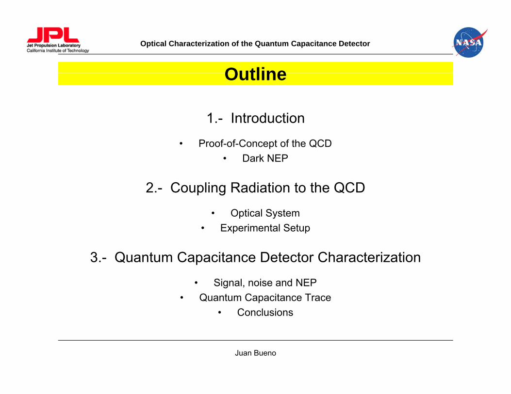
OutlineOutline
1.- Introduction1. Introduction
• Proof-of-Concept of the QCD• Dark NEP
2.- Coupling Radiation to the QCD
• Optical System • Experimental Setup
3.- Quantum Capacitance Detector Characterization
• Signal, noise and NEP• Quantum Capacitance Trace
• Conclusions
Juan Bueno

Optical Characterization of the Quantum Capacitance Detector
Proof of concept of the QCDProof-of-concept of the QCD
• Quasiparticles injected with a SIS junction
• NEP on the order of 10-18 W/Hz1/2
• Large scalabilityLarge scalability
• Next step: couple light to the detector
Juan Bueno

Optical Characterization of the Quantum Capacitance Detector
Detector SchemeDetector Scheme
• Radiation is absorbed by the antenna which is coupled to the absorber
• Cooper-pairs are broken and quasiparticles tunnel through the junctions
• The quasiparticle density is proportional to the quasiparticle tunneling rate
(our measurable quantity)
Juan Bueno
( q y)

Optical Characterization of the Quantum Capacitance Detector
Optical System (I)Optical System (I)29µm
2.1µm1.5µm
0.8µm
1.7µm
0.05µm15.9µm
1.4µm
• Double-dipole antenna
• Frequency = 1 5THz (λ = 200µm)
Juan Bueno
• Frequency = 1.5THz (λ = 200µm)

Optical Characterization of the Quantum Capacitance Detector
Optical System (II)Optical System (II)
• Z = 32Ω
• Resonance @ 1.5 THz
• 30% bandwidth
Juan Bueno
Optical Characterization of the Quantum Capacitance Detector
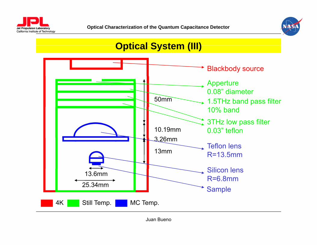
Optical System (III)Optical System (III)
Blackbody source
50mm 1.5THz band pass filter%
Apperture0.08” diameter
10.19mm3 26mm
10% band3THz low pass filter0.03” teflon
3.26mm
13mmTeflon lensR=13.5mm
Silicon lensSilicon lensR=6.8mmSample
13.6mm
25.34mm
Juan Bueno
4K Still Temp. MC Temp.

Optical Characterization of the Quantum Capacitance Detector
DetectorDetector
• Cooled down with a dilution refrigerator experiments done at 100mKCooled down with a dilution refrigerator, experiments done at 100mK
• Nb λ/2 resonator, Au antenna with Al absorber with Nb plug for quasiparticle trapping
• QCD out of Al/AlOx/Al
Juan Bueno

Optical Characterization of the Quantum Capacitance Detector
ResonanceResonance
• Resonance frequency = 3.328118 GHz
• Q = 150000• Q = 150000
• Peak depth = 6.5 dB
Juan Bueno

Optical Characterization of the Quantum Capacitance Detector
Qubit signalQubit signal
• Measured with a Lock-in amplifier technique
• Qubit biased with an AC tone at 25kHz
Juan Bueno

Optical Characterization of the Quantum Capacitance Detector
Sending light to the QCDSending light to the QCD
• Step the blackbody temperature from 5 to 40K
• Resonance moves towards the right
• Consistent with a drop of• Consistent with a drop of the quantum capacitance
signal
Juan Bueno

Optical Characterization of the Quantum Capacitance Detector
Measuring the noiseMeasuring the noise
• Noise measured with a spectrum analyzer at the
resonance frequencyresonance frequency
• Phase and amplitude noise measured for each
temperaturetemperature
• Ellipse of noise multiplied by 50 in the figure
Juan Bueno

Optical Characterization of the Quantum Capacitance Detector
Phase NEPPhase NEP
• Blackbody radiation couples to the detector in
the single mode
• Filter bandwidth = 10%
• Transmission = 60%
• Resonance frequency shifts 400Hz/K
• NEP about 10-17 W/Hz1/2
Juan Bueno

Optical Characterization of the Quantum Capacitance Detector
Thermal behavior of the resonatorThermal behavior of the resonator
• Two level systems could be the cause of the
frequency shiftq y
• Step the mixing chamber temperature
• In order to get the same frequency shift, the mixing
chamber should be at 300mK (too high!)( g )
Juan Bueno
Optical Characterization of the Quantum Capacitance Detector
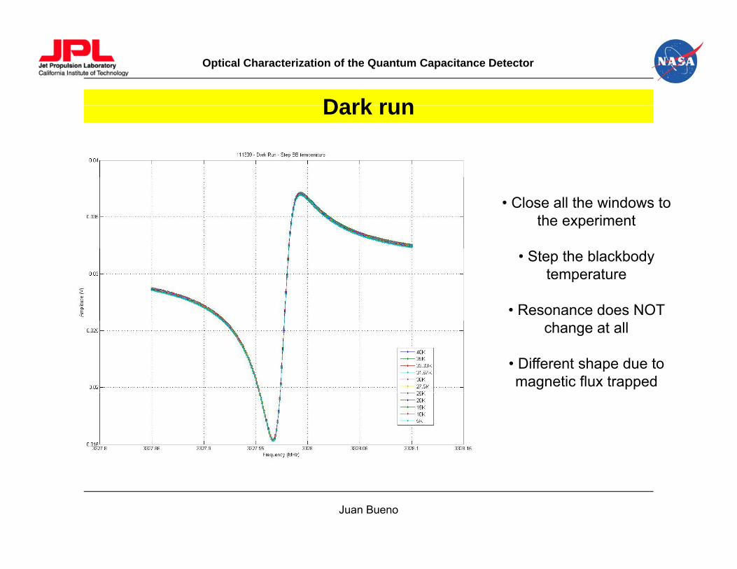
Dark runDark run
• Close all the windows to the experiment
• Step the blackbody temperature
• Resonance does NOT change at all
• Different shape due to magnetic flux trapped
Juan Bueno

Optical Characterization of the Quantum Capacitance Detector
Quantum Capacitance Trace (I)Quantum Capacitance Trace (I)
• Send a ramp to the gate and look at the signal with
an oscilloscopean oscilloscope
• No clear quantum capacitance peaks visible
• However, the signal drifts when an offset is applied to
the ramp
Juan Bueno

Optical Characterization of the Quantum Capacitance Detector
Quantum Capacitance Trace (II)Quantum Capacitance Trace (II)
St th t lt d• Step the gate voltage and use a lock-in technique to
look at the signal
N l t• No clear quantum capacitance peaks visible.
• Step the blackbody temperat re Some peakstemperature. Some peaks
grew, some peaks decreased
No clear conclusion can• No clear conclusion can be drawn
Juan Bueno

Optical Characterization of the Quantum Capacitance Detector
Quantum Capacitance Trace (III)Quantum Capacitance Trace (III)
~320 µm long 1 µm gap1 5 µm strip1.5 µm strip1 µm gap3 micron strip6 micron gap10 micron stripC f 10 micron strip6 micron gapCc = 0.45 fF
Vgate VCPWCc = 0.45 fF
C i l = 4 5pF
• Voltage divider
• VCPW = Vgate Cc / Cspiral
QCDCspiral 4.5pF
• This is possibly the reason why we do not see a clear quantum capacitance trace
Juan Bueno

Optical Characterization of the Quantum Capacitance Detector
Room for ImprovementRoom for Improvement
• Adding an extra line for gating the qubit and biasing g g q g
it at its degeneracy point
• Designing a new optimized optical systemp y
• Coupling the QCD to a better quality resonator
Juan Bueno
Optical Characterization of the Quantum Capacitance Detector
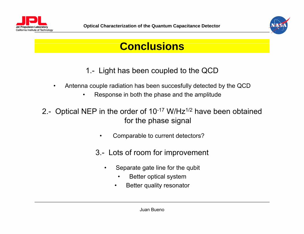
C l iConclusions
1.- Light has been coupled to the QCD1. Light has been coupled to the QCD
• Antenna couple radiation has been succesfully detected by the QCD• Response in both the phase and the amplitude
2.- Optical NEP in the order of 10-17 W/Hz1/2 have been obtained for the phase signal
• Comparable to current detectors?
3.- Lots of room for improvement
• Separate gate line for the qubit• Better optical system
• Better quality resonator
Juan Bueno


![Quantum Non-Markovianity: Characterization, Quantification ...arXiv:1405.0303v2 [quant-ph] 24 Aug 2014 REVIEW ARTICLE Quantum Non-Markovianity: Characterization, Quantification and](https://img.pdfslide.us/doc/110x75/5f686450aac7fc0d604af5b8/quantum-non-markovianity-characterization-quantiication-arxiv14050303v2.jpg)