Embed Size (px)
Citation preview
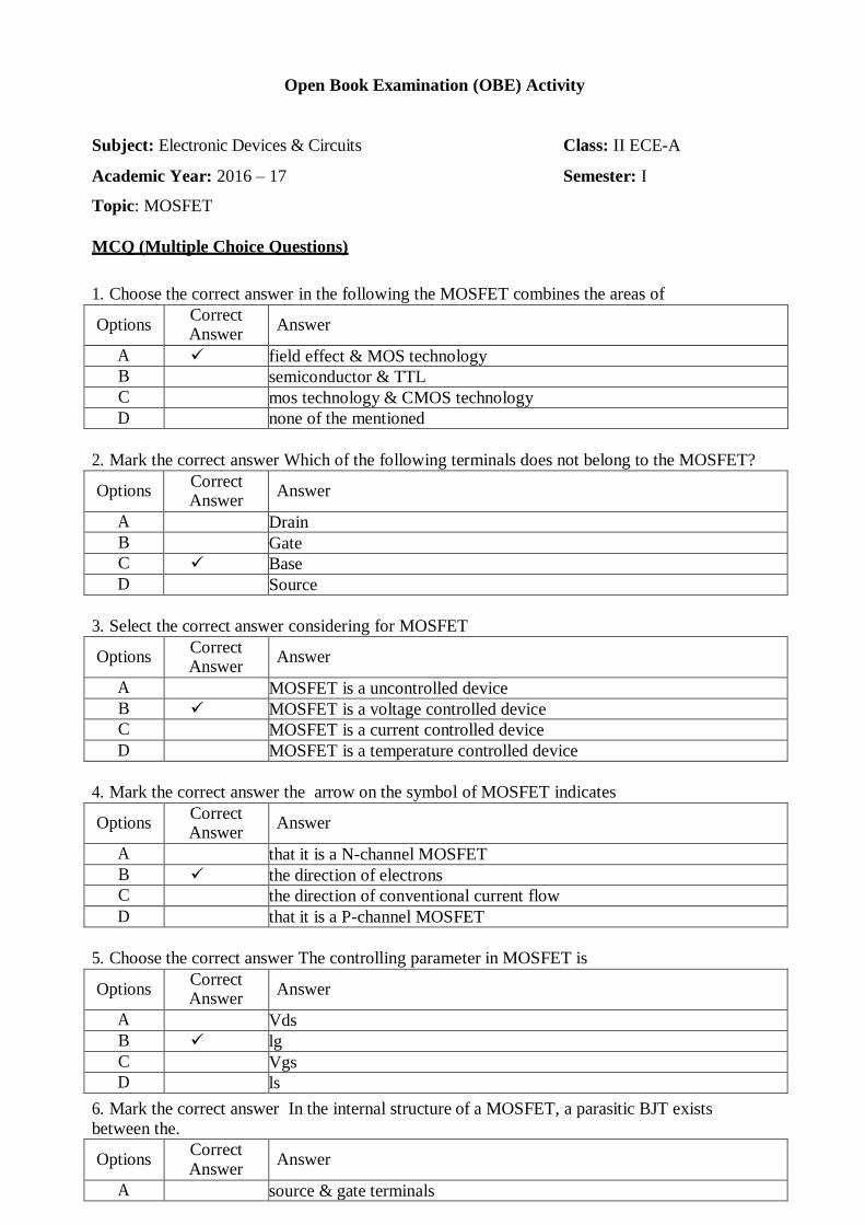
Open Book Examination (OBE) Activity
Subject: Electronic Devices & Circuits Class: II ECE-A
Academic Year: 2016 – 17 Semester: I
Topic: MOSFET
MCQ (Multiple Choice Questions)
1. Choose the correct answer in the following the MOSFET combines the areas of
Options Correct Answer
Answer
A field effect & MOS technology
B semiconductor & TTL
C mos technology & CMOS technology
D none of the mentioned
2. Mark the correct answer Which of the following terminals does not belong to the MOSFET?
Options Correct Answer
Answer
A Drain
B Gate
C Base
D Source
3. Select the correct answer considering for MOSFET
Options Correct Answer
Answer
A MOSFET is a uncontrolled device
B MOSFET is a voltage controlled device
C MOSFET is a current controlled device
D MOSFET is a temperature controlled device
4. Mark the correct answer the arrow on the symbol of MOSFET indicates
Options Correct Answer
Answer
A that it is a N-channel MOSFET
B the direction of electrons
C the direction of conventional current flow
D that it is a P-channel MOSFET
5. Choose the correct answer The controlling parameter in MOSFET is
Options Correct Answer
Answer
A Vds
B lg
C Vgs
D ls
6. Mark the correct answer In the internal structure of a MOSFET, a parasitic BJT exists
between the.
Options Correct Answer
Answer
A source & gate terminals
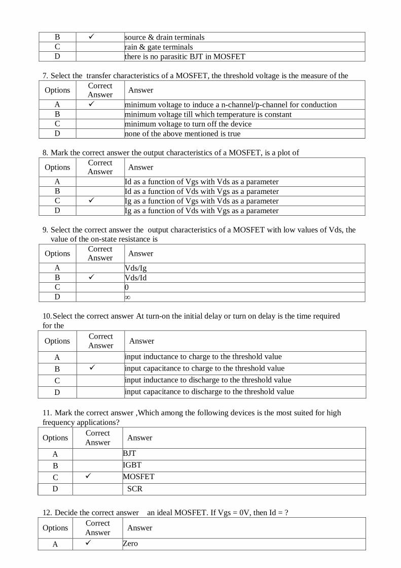
B source & drain terminals
C rain & gate terminals
D there is no parasitic BJT in MOSFET
7. Select the transfer characteristics of a MOSFET, the threshold voltage is the measure of the
Options Correct Answer
Answer
A minimum voltage to induce a n-channel/p-channel for conduction
B minimum voltage till which temperature is constant
C minimum voltage to turn off the device
D none of the above mentioned is true
8. Mark the correct answer the output characteristics of a MOSFET, is a plot of
Options Correct Answer
Answer
A Id as a function of Vgs with Vds as a parameter
B Id as a function of Vds with Vgs as a parameter
C Ig as a function of Vgs with Vds as a parameter
D Ig as a function of Vds with Vgs as a parameter
9. Select the correct answer the output characteristics of a MOSFET with low values of Vds, the
value of the on-state resistance is
Options Correct Answer
Answer
A Vds/Ig
B Vds/Id
C 0
D ∞
10. Select the correct answer At turn-on the initial delay or turn on delay is the time required
for the
Options Correct
Answer Answer
A input inductance to charge to the threshold value
B input capacitance to charge to the threshold value
C input inductance to discharge to the threshold value
D input capacitance to discharge to the threshold value
11. Mark the correct answer ,Which among the following devices is the most suited for high
frequency applications?
Options Correct
Answer Answer
A BJT
B IGBT
C MOSFET
D SCR
12. Decide the correct answer an ideal MOSFET. If Vgs = 0V, then Id = ?
Options Correct
Answer Answer
A Zero
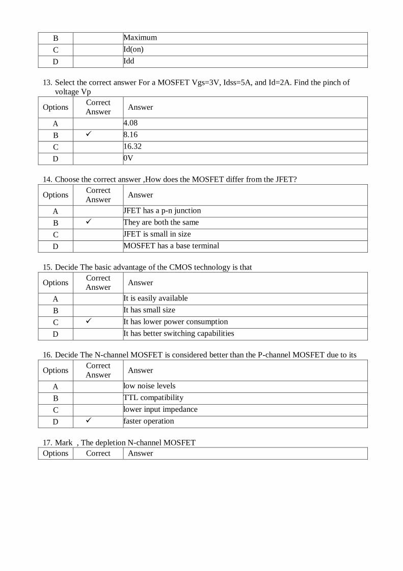
B Maximum
C Id(on)
D Idd
13. Select the correct answer For a MOSFET Vgs=3V, Idss=5A, and Id=2A. Find the pinch of
voltage Vp
Options Correct
Answer Answer
A 4.08
B 8.16
C 16.32
D 0V
14. Choose the correct answer ,How does the MOSFET differ from the JFET?
Options Correct
Answer Answer
A JFET has a p-n junction
B They are both the same
C JFET is small in size
D MOSFET has a base terminal
15. Decide The basic advantage of the CMOS technology is that
Options Correct
Answer Answer
A It is easily available
B It has small size
C It has lower power consumption
D It has better switching capabilities
16. Decide The N-channel MOSFET is considered better than the P-channel MOSFET due to its
Options Correct
Answer Answer
A low noise levels
B TTL compatibility
C lower input impedance
D faster operation
17. Mark , The depletion N-channel MOSFET
Options Correct Answer

Answer
A Can be operated as a JFET with zero gate voltage
B Can be operated as an enhancement MOSFET by applying +ve bias to
gate
C Can be operated as an enhancement MOSFET by applying -ve bias to gate
D Cannot be operated as an enhancement MOSFET
18. Select the correct answer MOSFET has greatest application in digital circuit due to
Options Correct
Answer Answer
A Low power consumption
B Less noise
C Small amount of space it takes on a chip
D All of the above
19. Select The enhancement N-channel MOSFET
Options Correct
Answer Answer
A Cannot be operated as an enhancement MOSFET
B Can be operated as a JFET with zero gate voltage
C Can be operated as an enhancement MOSFET by applying -ve bias to gate
D Can be operated as an enhancement MOSFET by applying +ve bias to
gate
20. Decide The MOSFET stands for
Options Correct
Answer Answer
A Metal oxidized selenium FET
B Metal oxide surface FET
C Metal oxide semiconductor FET
D Metal of surface FET
21. Mark correct answer ,The enhancement MOSFET is
Options Correct
Answer Answer
A Normally of MOSFET
B Useful as a very good constant voltage source
C Widely used because of easy in its fabrication
D Normally on MOSFET
.

22. Choose the correct answer In MOSFETs N-channel is more preferred than P-channel
because
Options Correct
Answer Answer
A It is cheaper
B It is faster
C It has better drive capability
D It has better noise immunity
23. Decide the MOSFET is almost ideal as switching device because
Options Correct
Answer Answer
A It has longer life
B It works progressively
C It consumes low power
D It has linear characteristics
24. Choose IGFET is a ................ device
Options Correct
Answer Answer
A Linear
B Logarithmic
C Half power
D Square law
25. Choose the correct answer ,The main types of field effect transistor are
Options Correct
Answer Answer
A BJT and FET
B UJT and FET
C JFET and MOSFET
D None of the above
26. Mark the input gate current of a FET is
Options Correct
Answer Answer
A A few micro-amperes
B A few mili-amperes
C A few amperes
D Negligible
27. Decide, The transistor can be operated in
Options Correct
Answer Answer

A Active region
B Saturation region
C Cut-off region
D All of the above regions
28. Select the arrow in a transistor terminal represents
Options Correct
Answer Answer
A Emitter
B Collector
C Base
D None of the above
29. Select the correct answer ,The germanium transistors can be used upto
Options Correct
Answer Answer
A 600C
B 1000C
C 1500C
D 3000C
30. Decide A transistor is said to be operating in the cut-off region if
Options Correct
Answer Answer
A Emitter junction is forward biased and collector junction is forward biased
B Emitter junction is reverse biased and collector junction is reverse biased
C Emitter junction is reverse biased and collector junction is forward biased
D Emitter junction is forward biased and collector junction is reverse biased
31. Select the Transistor is a device which is a
Options Correct
Answer Answer
A Transferring voltage device
B Current operated one
C Power operated one
D Voltage operated one
32. Select, The transistor can transfer
Options Correct
Answer Answer
A A signal from low resistance to high resistance
B A weak signal of only higher frequencies through it
C A weak signal of only lower frequencies through it
D A signal from high resistance to low resistance
33. Choose the correct answer When the transistor is in saturation, the collector to emitter voltage
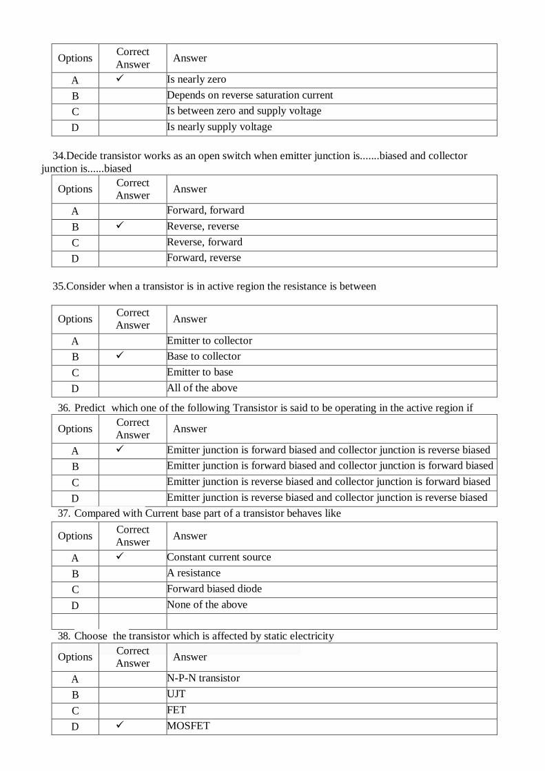
Options Correct
Answer Answer
A Is nearly zero
B Depends on reverse saturation current
C Is between zero and supply voltage
D Is nearly supply voltage
34.Decide transistor works as an open switch when emitter junction is.......biased and collector
junction is......biased
Options Correct
Answer Answer
A Forward, forward
B Reverse, reverse
C Reverse, forward
D Forward, reverse
35.Consider when a transistor is in active region the resistance is between
Options Correct
Answer Answer
A Emitter to collector
B Base to collector
C Emitter to base
D All of the above
36. Predict which one of the following Transistor is said to be operating in the active region if
Options Correct
Answer Answer
A Emitter junction is forward biased and collector junction is reverse biased
B Emitter junction is forward biased and collector junction is forward biased
C Emitter junction is reverse biased and collector junction is forward biased
D Emitter junction is reverse biased and collector junction is reverse biased
37. Compared with Current base part of a transistor behaves like
Options Correct
Answer Answer
A Constant current source
B A resistance
C Forward biased diode
D None of the above
38. Choose the transistor which is affected by static electricity
Options Correct
Answer Answer
A N-P-N transistor
B UJT
C FET
D MOSFET
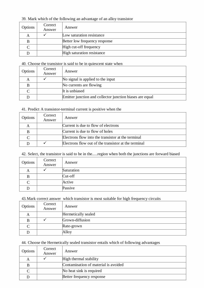
39. Mark which of the following an advantage of an alloy transistor
Options Correct
Answer Answer
A Low saturation resistance
B Better low frequency response
C High cut-off frequency
D High saturation resistance
40. Choose the transistor is said to be in quiescent state when
Options Correct
Answer Answer
A No signal is applied to the input
B No currents are flowing
C It is unbiased
D Emitter junction and collector junction biases are equal
41. Predict A transistor-terminal current is positive when the
Options Correct
Answer Answer
A Current is due to flow of electrons
B Current is due to flow of holes
C Electrons flow into the transistor at the terminal
D Electrons flow out of the transistor at the terminal
42. Select, the transistor is said to be in the.....region when both the junctions are forward biased
Options Correct
Answer Answer
A Saturation
B Cut-off
C Active
D Passive
43. Mark correct answer which transistor is most suitable for high frequency circuits
Options Correct
Answer Answer
A Hermetically sealed
B Grown-diffusion
C Rate-grown
D Alloy
44. Choose the Hermetically sealed transistor entails which of following advantages
Options Correct
Answer Answer
A High thermal stability
B Contamination of material is avoided
C No heat sink is required
D Better frequency response

45. Decide In CB configuration, a transistor transfers
Options Correct
Answer Answer
A Voltage from high impedance circuit to low impedance
B Voltage from low impedance circuit to high impedance
C Current from high impedance circuit to low impedance circuit
D Current from low impedance circuit to high impedance circuit
46. Select the correct answer A transistor acts like a diode and
Options Correct
Answer Answer
A Power supply
B Current source
C Resistance
D Voltage source
47. Choose the correct answer A MOSFET can be operated with
Options Correct
Answer Answer
A negative gate voltage only
B positive gate voltage only
C positive as well as negative gate voltage
D none of the above
Options Correct
Answer Answer
A many gate
B open gate
C insulated gate
D shorted gate
Options Correct
Answer Answer
A capacitor
B battery
C generator
D none of the above
Options Correct
Answer Answer
A Ω
B a few hundred Ω
C kΩ
D several MΩ
48. Mark A MOSFET is sometimes called ………. JFET
49. Decide A MOSFET uses the electric field of a ………. to control the channel
current
50. Select the input impedance of a MOSFET is of the order of
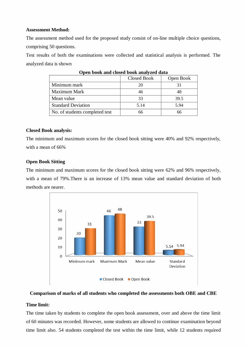
Assessment Method:
The assessment method used for the proposed study consist of on-line multiple choice questions,
comprising 50 questions.
Test results of both the examinations were collected and statistical analysis is performed. The
analyzed data is shown
Open book and closed book analyzed data
Closed Book Open Book
Minimum mark 20 31
Maximum Mark 46 48
Mean value 33 39.5
Standard Deviation 5.14 5.94
No. of students completed test 66 66
Closed Book analysis:
The minimum and maximum scores for the closed book sitting were 40% and 92% respectively,
with a mean of 66%
Open Book Sitting
The minimum and maximum scores for the closed book sitting were 62% and 96% respectively,
with a mean of 79%.There is an increase of 13% mean value and standard deviation of both
methods are nearer.
Comparison of marks of all students who completed the assessments both OBE and CBE
Time limit:
The time taken by students to complete the open book assessment, over and above the time limit
of 60 minutes was recorded. However, some students are allowed to continue examination beyond
time limit also. 54 students completed the test within the time limit, while 12 students required

additional time to complete the assessment.
The influence of time on students marks in the open book sitting
Completed in < 60 min Completed in > 60 min
Marks Marks Extra time in
min
Minimum Mark 29 30 5
Maximum mark 48 42 14
Mean Value 40.38 35.63 9.13
Standard deviation 5.91 4.10 2.85
No, of students completed test 54 6 6
Students completed in < 60 min:
The minimum and maximum scores for the open book sitting were 58% and 98% respectively,
with a mean of 80.76%
Students exceeded 60 min:
The minimum and maximum scores for the open book sitting were 60% and 84% respectively,
with a mean of 71.26%
Comparison of open book sitting marks of students who completed in < 60 min time and >
60 min.
Post Reflections:
There is a significant improvement in minimum mark and mean value Open book
Examination. The increase of 13.34% in mean for open book test shows that the average
mark of most of the students is increased, which it indicates that there is an improvement in
students performance in OBE sitting when considered average marks.
The maximum mark in OBE and CBE sittings is almost same and only two marks difference
(48 and 47 marks respectively) for intelligent student whether it is open book or closed book
examination is immaterial.
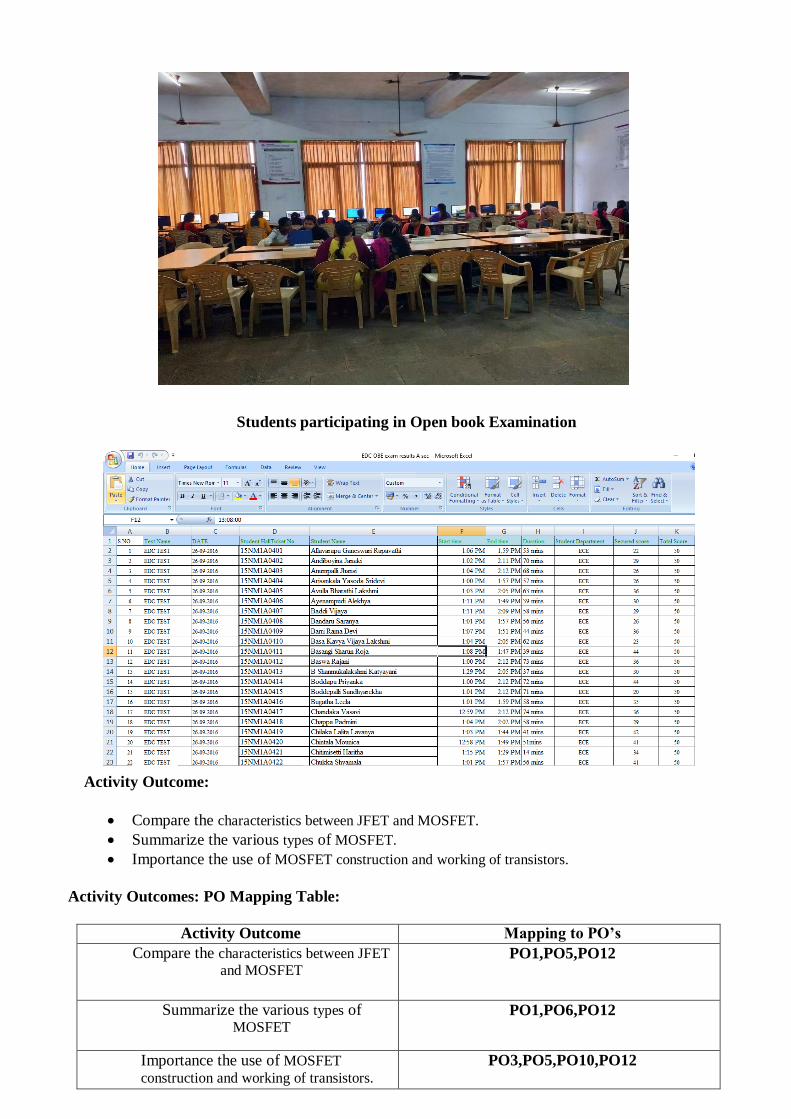
Students participating in Open book Examination
Activity Outcome:
Compare the characteristics between JFET and MOSFET.
Summarize the various types of MOSFET.
Importance the use of MOSFET construction and working of transistors.
Activity Outcomes: PO Mapping Table:
Activity Outcome Mapping to PO’s
Compare the characteristics between JFET
and MOSFET PO1,PO5,PO12
Summarize the various types of MOSFET
PO1,PO6,PO12
Importance the use of MOSFET
construction and working of transistors. PO3,PO5,PO10,PO12

Post Implications:
All the students actively taken the test conducted in open book exam.
Few students were felt hard during closed book exam.
Few students were enthusiastic to refer standard reference books to learn and understand
the concept.

![T.Y. B.Sc. (Semester – III) Examination, 2011 ELECTRONIC ... · [4017] – 366 T.Y. B.Sc. (Semester – III) Examination, 2011 ELECTRONIC SCIENCE (Paper – V ... (Vocational) (Semester](https://img.pdfslide.us/doc/110x75/5b7e27757f8b9abe0e8d5757/ty-bsc-semester-iii-examination-2011-electronic-4017-366.jpg)