Embed Size (px)
Citation preview
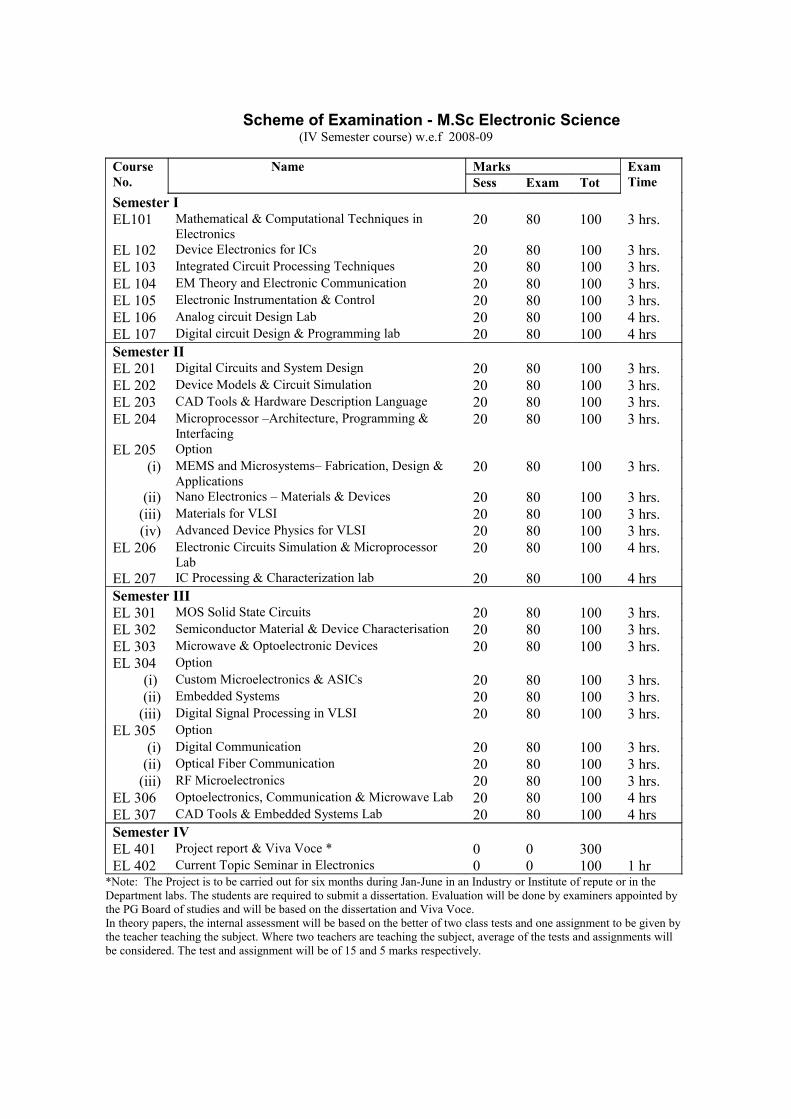
Scheme of Examination - M.Sc Electronic Science(IV Semester course) w.e.f 2008-09
Course No.
Name Marks Exam TimeSess Exam Tot
Semester IEL101 Mathematical & Computational Techniques in
Electronics20 80 100 3 hrs.
EL 102 Device Electronics for ICs 20 80 100 3 hrs.EL 103 Integrated Circuit Processing Techniques 20 80 100 3 hrs.EL 104 EM Theory and Electronic Communication 20 80 100 3 hrs.EL 105 Electronic Instrumentation & Control 20 80 100 3 hrs.EL 106 Analog circuit Design Lab 20 80 100 4 hrs.EL 107 Digital circuit Design & Programming lab 20 80 100 4 hrsSemester IIEL 201 Digital Circuits and System Design 20 80 100 3 hrs.EL 202 Device Models & Circuit Simulation 20 80 100 3 hrs.EL 203 CAD Tools & Hardware Description Language 20 80 100 3 hrs.EL 204 Microprocessor –Architecture, Programming &
Interfacing20 80 100 3 hrs.
EL 205 Option(i) MEMS and Microsystems– Fabrication, Design &
Applications20 80 100 3 hrs.
(ii) Nano Electronics – Materials & Devices 20 80 100 3 hrs.(iii) Materials for VLSI 20 80 100 3 hrs.(iv) Advanced Device Physics for VLSI 20 80 100 3 hrs.
EL 206 Electronic Circuits Simulation & Microprocessor Lab
20 80 100 4 hrs.
EL 207 IC Processing & Characterization lab 20 80 100 4 hrsSemester IIIEL 301 MOS Solid State Circuits 20 80 100 3 hrs.EL 302 Semiconductor Material & Device Characterisation 20 80 100 3 hrs.EL 303 Microwave & Optoelectronic Devices 20 80 100 3 hrs.EL 304 Option
(i) Custom Microelectronics & ASICs 20 80 100 3 hrs.(ii) Embedded Systems 20 80 100 3 hrs.
(iii) Digital Signal Processing in VLSI 20 80 100 3 hrs.EL 305 Option
(i) Digital Communication 20 80 100 3 hrs.(ii) Optical Fiber Communication 20 80 100 3 hrs.
(iii) RF Microelectronics 20 80 100 3 hrs.EL 306 Optoelectronics, Communication & Microwave Lab 20 80 100 4 hrsEL 307 CAD Tools & Embedded Systems Lab 20 80 100 4 hrsSemester IVEL 401 Project report & Viva Voce * 0 0 300EL 402 Current Topic Seminar in Electronics 0 0 100 1 hr
*Note: The Project is to be carried out for six months during Jan-June in an Industry or Institute of repute or in the Department labs. The students are required to submit a dissertation. Evaluation will be done by examiners appointed by the PG Board of studies and will be based on the dissertation and Viva Voce. In theory papers, the internal assessment will be based on the better of two class tests and one assignment to be given by the teacher teaching the subject. Where two teachers are teaching the subject, average of the tests and assignments will be considered. The test and assignment will be of 15 and 5 marks respectively.

EL 101 Mathematical & Computational Techniques in ElectronicsInstructions: There shall be nine questions in total. Question number 1 will be compulsory and will consist of short conceptual type answers covering all the Units. There shall be eight more questions, two from each unit. Students are required to attempt four questions, selecting one from each unit in addition to the compulsory question. All questions will carry equal marks.
Maximum Marks: 80, Time = 3 hoursInternal Assessment: 20 Marks
Unit 1
DC Analysis of Linear Networks, Different kinds of Analysis, Network graphs: basic concepts, formation of incidence matrix and its properties, Cut set matrix, Transient Analysis of Linear and Non-linear Circuits, Possible Formulation Techniques, Numerical solution of ordinary differential equations, Associated Circuit Models for Inductors and Capacitors, Use of Associated Circuit Models, Monte Carlo Method, Mixed Mode Simulator.
Unit IIDC analysis of Non-Linear circuits, DC analysis of Non-Linear Equation in one unknown, Newton-Raphson Techniques for many variables, Linearised Equivalent for Newton-Raphson Technique, Linearised Equivalent Circuit for Hybrid Formulation, General Consideration in solving Non-linear Circuits, State variable analysis: Introduction, State Space model, Continuous-time model, State-Space model applicable for electrical circuits.
Unit IIIOperational Methods in Applied Mathematics; Integral Transform, Application of the Operational Calculus to the solution of partial Differential Equations, Evaluation of Integrals, Applications of the Laplace Transform to the solution of Linear Integral Equations. Laplace Transforms, Fundamental rules, Calculation of Direct & Indirect Transforms, Laplace Transforms of Periodic functions, Systems of Linear Differential Equations with constant Coefficient, solving electrical circuits using Laplace transform.
Unit IVDigital Signal Analysis, Continuous and discrete-time signal, sampling theorem, Fourier series, Examples of Fourier Expansions of Functions, Fourier transform and its properties, applications of Fourier transform in circuit analysis, Discrete Fourier Transform and its properties, DFT and Fourier transform, Relation to the Fourier Transform: Aliasing, DFT and Fourier series, Fast Fourier Transform, Redundancy in the DFT, Sample Set Decomposition, Z-transform: definition, Z-transforms of some common sequences, Properties of the Z-transforms.
References:1. Applied Mathematics for Engineers and Physicists by Louis A. Pipes and Lawrence R. Harvill.2. Digital Signal Analysis by Samuel D. Stearns and Don R. Hush.3. Computer Simulation of Electronic Circuits by R. Raghuram.4. Scientific and Engineering Applications with PC's by Raymond Annino & Richard Drives.5. Schaum's Outline of Laplace Transforms by Murray R Spiegel (Author)6. Schaum's Outline of Signals and Systems by Hwei Hsu (Author)7. Circuit Theory by Abhijit Chakrabarthi, Dhanpat Rai & Sons.8. Basic Engineering Circuit Analysis by J. David Irwin, 3rd Ed., Macmillan Publishing Company, New York.

EL 102 – Device Electronics for ICs
Instructions: There shall be nine questions in total. Question number 1 will be compulsory and will consist of short conceptual type answers covering all the Units. There shall be eight more questions, two from each unit. Students are required to attempt four questions, selecting one from each unit in addition to the compulsory question. All questions will carry equal marks.
Maximum Marks: 80, Time = 3 hoursInternal Assessment: 20 Marks
Unit IPhysics of semiconductor materials, Band model of solids, Thermal equilibrium statistics, Inhomogenously doped semiconductors, free carriers in semiconductors, Mobility and scattering, Diffusion current, The p-n junction, Reverse-biased pn junctions, Junction Break down, The junction FET, MESFET, Continuity Equations, Generation & Recombination, Current-voltage characteristics of pn junctions Hetrojunctions
Unit IITransistor Action, Active bias, Transistor switching, Amplifying and switching transistors, Ebers-Moll Model, Hetrojunction bipolar transistor, Double hetrojunction BJT, Bandgap grading in base, Effects of collector bias variation, Effects at low and high emitter bias, base transit time, charge-control model. Small signal transistor model, Frequency limitation of bipolar transistors, Bipolar models for computer simulation.
Unit IIIEquilibrium in Electronic System, Idealized Metal-semiconductor junction, Current-voltage characteristics, Non rectifying contacts, Surface effects, MOS structure, Capacitance of MOS system, MOS Electronics, Oxide of Interface charges, Basic MOSFET behaviour, Improved Models for short channel MOSFETs.
Unit IVScaling of MOSFETs, Gate coupling, velocity overshoot, high field effects, substrate current, Hot carrier effects, Gate current, Device degradation, Structure that reduce the drain field.Numerical simulation, Basic concept of simulation, Grids, Device simulation, simulation challenges
References:1. Device Electronics for Integrated circuits by R.S. Muller & T. I. Kamins &
Mansun Chang (Third edition) John Wiley & Sons 2. Physics and Technology of Semiconductor Devices by A.S. Grove.3. Physics of Semiconductor Devices by S.M.Sze.4. VLSI Electronic Microstructure Science, Vol 10, eds. N.G. Einspruch & R.S.Bauer, Academic Press.

EL 103 - Integrated Circuit Processing Techniques
Instructions: There shall be nine questions in total. Question number 1 will be compulsory and will consist of short conceptual type answers covering all the Units. There shall be eight more questions, two from each unit. Students are required to attempt four questions, selecting one from each unit in addition to the compulsory question. All questions will carry equal marks.
Maximum Marks: 80, Time = 3 hoursInternal Assessment: 20 Marks
Unit IMicroelectronics processing: Introduction, Clean Room, Pure Water System, Vacuum Science and Technology, Practical vacuum systems, Operating principle: Rotary Pump, Diffusion pump, Cryo Pump and Turbo Pump, Vacuum Gauges: Pirani and Penning and Ionization Gauge, Sources for vacuum deposition, Sputtering (DC, RF and RF Magnetron), Chemical Vapor Deposition, reactors for chemical vapor deposition, CVD Applications, PECVD, Metallization, Epitaxy: Introduction, Vapor phase epitaxy, Liquid phase epitaxy and Molecular beam epitaxy, Hetroepitaxy.
Unit IIThermal Oxidation of Silicon, Oxide Formation, Kinetics of Oxide Growth, Oxidation Systems, Properties of Thermal Oxides of Silicon, Impurity Redistribution during Oxidation,Uses of Silicon Oxide, Basic diffusion process, Diffusion Equation, Diffusion Profiles, Evaluation of Diffused Layers, Diffusion in Silicon, Emitter-Push Effect, Lateral Diffusion, Distribution and Range of Implanted Ions, Ion Distribution, Ion Stopping, Ion Channeling, Disorder and Annealing, Multiple Implantation and Masking, Pre-deposition and Threshold Control.
Unit IIIPhotolithography, Negative and Positive Photoresist, Resist Application, Exposure and Development, Photolithographic Process Control. E-Beam Lithography, X-Ray Beam Lithography and Ion Beam Lithography. Wet Chemical Etching, Chemical Etchants for SiO2, Si3N4, Polycristalline Silicon and other microelectronic materials, Plasma Etching, Plasma Etchants, Photoresist Removal, Lift off process, Etch Process Control,
Unit IVFundamental considerations for I.C processing, PMOS and NMOS IC Technology, CMOS I.C technology, MOS Memory technology- Static and Dynamic, Bipolar IC Technology, BiCMOS Technology, Packaging design considerations, Special package considerations, Yield loss in VLSI, Reliability requirements for VLSI.
References:1. Microchip Fabrication: A Practical Guide to Semiconductor Processing by Peter Van Zant (2nd Edition)
(McGraw Hill Publishing Company).2. Vacuum Technology by A. Roth3. Microelectronic Processing: An Introduction to the Manufacture of Integrated Circuits by W. Scot
Ruska (McGraw Hill International Edition).4. VLSI Technology By S.M.Sze (2nd Edition)5. Semiconductor Devices: Physics and Technology by S.M. Sze.6. VLSI Fabrication Principles: Silicon and Gallium Arsenide by Sorab K. Ghandhi (John Wiley & Sons).7. Fundamentals of Microelectronic Processing by Hong H. Lee (McGraw Hill Chemical Engineering
Series).8. Thin Film Processes Part I & II by John L. Vossen and Wirner Kern (Academic Press).

EL 104 – EM Theory and Electronic Communication
Instructions: There shall be nine questions in total. Question number 1 will be compulsory and will consist of short conceptual type answers covering all the Units. There shall be eight more questions, two from each unit. Students are required to attempt four questions, selecting one from each unit in addition to the compulsory question. All questions will carry equal marks.
Maximum Marks: 80, Time = 3 hoursInternal Assessment: 20 Marks
Unit IWave Equation and Boundary conditions, Plane monochromatic wave in non-conducting media, conducting media, Reflection and refraction at the boundary of two non-conducting media-oblique incidence, Reflection from a conducting plane-total internal reflection, Propagation between parallel conducting plates, Radio Wave propagation: Propagation in Free space, Tropospheric Propagation, Ionospheric propagation,Surface wave propagation, Sky wave propagation, Propagation losses.
Unit IITransmission lines, Characteristic impedance, standing waves, quarter and half wavelength lines,Impedance matching, Use of Smith Chart, Impedance matching using Smith Chart, Losses in Transmission lines, Wave-guides: Rectangular, losses in Wave-guides, S Parameters, Pulse excitation, Basics of Antennas: Antenna parameters, Dipole antennas, Radiation pattern, Antenna gain.
Unit IIIPulse Communication, Pulse Amplitude modulation (PAM), Pulse Width Modulation, Pulse PositionModulation (PPM), Pulse Code Modulation and application.Digital Communication, Characteristics of Data Transmission Circuit, Data Transmission speeds, Noise,Cross talks, Echo suppressors, Distortion, Equalizers, Bit transmission, Signaling rate, DigitalCommunication techniques, FSK, PSK, BPSK, QPSK, DPSK. Error Detection and Correction codes.
Unit IVModern Telephone networks, ISDN, mobile telephone network, intelligent network and services (in brief)Satellite Communication: Introduction, Orbits, Station keeping, Satellite Attitude, Transmission Path, PathLoss, Noise considerations, the Satellite Systems, Saturation flux density, Effective Isotropic radiatedPower, Multiple Access Methods.
References:
1. Foundations of Electromagnetic Theory JR Reitz and FZ by Reitz and Milford (Addison Wesley).2. Electromagnetics by B.B.Land (Wiley Eastern).3. Basic Electromagnetic fields by H.P. Neff (Harper & Row).4. Theory and Applications of Microwaves by Brownwell and Beam (McGraw Hill).5. Advanced Electronic Communication by Gray M.Miller.6. Electronic Communication by George Kennedy.7. Basic Electronic Communication by Roody & Coolen.8. Satellite Communication by Robert M. Gagliord.9. Electronic Communication System by W.Tomasi10. Networks and Telecommunication Design & Operation by Martin.P.Clark11. Digital Communication with Fiber Optics and Satellite Application by Harold.B.Killen.

EL 105 Electronic Instrumentation & Control
Instructions: There shall be nine questions in total. Question number 1 will be compulsory and will consist of short conceptual type answers covering all the Units. There shall be eight more questions, two from each unit. Students are required to attempt four questions, selecting one from each unit in addition to the compulsory question. All questions will carry equal marks.
Maximum Marks: 80, Time = 3 hoursInternal Assessment: 20 Marks
Unit I Basic concepts of measurement: Introduction, system configuration basic characteristics of measuring devices, Transducer Classification :Introduction, Electrical transducer, classification, basic requirementsPerformance characteristics of an instrumentation system: generalized system, zero order, first order, second order system, Measurement of displacement: principle of transduction, Variable resistance device, LVDT, Variable capacitance transducer, Hall effect devices, Measurement of pressure: Thin film pressure transducer, piezoelectric pressure transducer vibrating element pressure transducerMeasurement of position, velocity, force, torque (basics only)
Unit IIMeasurement of flow: Head type flow meters based on differential pressure measurements, AnemometersTemperature measurements: resistance type temp. sensors, thermistors, thermocouples, solid state sensors, optical pyrometersMeasurement of humidity, thickness, pH (basics only)Instrumentation amplifier, Signal processing, manipulation and transmission, Data acquisition systemsQ meter, Digital storage oscilloscope, Lock-in Amplifier, Bioelectrical signals and their measurment, Electrodes for ECG , transducer for blood pressure measurement
Unit IIIControl System: Introduction: Basic components of a control system, Example of control system applications, Open loop and closed loop control system, Feedback and its effects, Types of feedback control systems, Transfer functions, block diagram Signal flow graphs, Root loci technique for ananlyis of lTI control system, Bode plots and Nyquist plots
Unit IVStability of linear control systems : introduction, Methods of determining stability- Routh –Hurwitz stability, Nyquist Stability CriterionDesign of Control system: Design with P, I PD, PI and PID controllerControlling speed, temperature and position using analog/digital circuits
References1. Modern Electronic Instrumentation and Measurement Technique by Alfred D. Helfrick and William D.
Cooper, Eastern Economy Edition2. Instrumentation Devices and Systems by C.S. Rangan, G.R. Sarma and V.S.V Mani, Tata McGraw Hill3. Principles of Measurement and Instrumentation by Alan S. Morris, Prentice Hall 4. Automatic Control Systems by Benjamin C. Kuo, Prentice Hall India5. Modern Control Engineering by K. Ogata, PHI6. Bio-Medical Instrumentation By R.S Khandpur
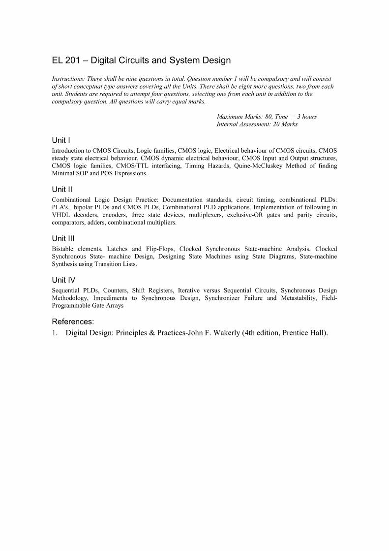
EL 201 – Digital Circuits and System Design
Instructions: There shall be nine questions in total. Question number 1 will be compulsory and will consist of short conceptual type answers covering all the Units. There shall be eight more questions, two from each unit. Students are required to attempt four questions, selecting one from each unit in addition to the compulsory question. All questions will carry equal marks.
Maximum Marks: 80, Time = 3 hoursInternal Assessment: 20 Marks
Unit IIntroduction to CMOS Circuits, Logic families, CMOS logic, Electrical behaviour of CMOS circuits, CMOS steady state electrical behaviour, CMOS dynamic electrical behaviour, CMOS Input and Output structures, CMOS logic families, CMOS/TTL interfacing, Timing Hazards, Quine-McCluskey Method of finding Minimal SOP and POS Expressions.
Unit IICombinational Logic Design Practice: Documentation standards, circuit timing, combinational PLDs: PLA's, bipolar PLDs and CMOS PLDs, Combinational PLD applications. Implementation of following in VHDL decoders, encoders, three state devices, multiplexers, exclusive-OR gates and parity circuits, comparators, adders, combinational multipliers.
Unit IIIBistable elements, Latches and Flip-Flops, Clocked Synchronous State-machine Analysis, Clocked Synchronous State- machine Design, Designing State Machines using State Diagrams, State-machine Synthesis using Transition Lists.
Unit IVSequential PLDs, Counters, Shift Registers, Iterative versus Sequential Circuits, Synchronous Design Methodology, Impediments to Synchronous Design, Synchronizer Failure and Metastability, Field-Programmable Gate Arrays
References:1. Digital Design: Principles & Practices-John F. Wakerly (4th edition, Prentice Hall).
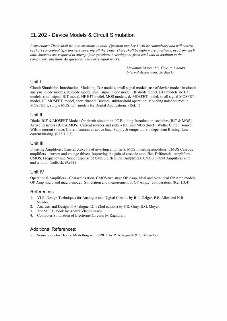
EL 202 - Device Models & Circuit Simulation
Instructions: There shall be nine questions in total. Question number 1 will be compulsory and will consist of short conceptual type answers covering all the Units. There shall be eight more questions, two from each unit. Students are required to attempt four questions, selecting one from each unit in addition to the compulsory question. All questions will carry equal marks.
Maximum Marks: 80, Time = 3 hoursInternal Assessment: 20 Marks
Unit ICircuit Simulation-Introduction, Modeling, D-c models, small signal models, use of device models in circuit analysis, diode models, dc diode model, small signal diode model, HF diode model, BJT models, dc BJT models, small signal BJT model, HF BJT model, MOS models, dc MOSFET model, small signal MOSFET model, HF MOSFET model, short channel Devices, subthreshold operation, Modeling noise sources in MOSFET’s, simple MOSFET models for Digital Applications. (Ref. 1)
Unit IIDiode, BJT & MOSFET Models for circuit simulation. IC Building-Introduction, switches (BJT & MOS), Active Resistors (BJT & MOS), Current sources and sinks - BJT and MOS (brief), Widlar Current source, Wilson current source, Current sources as active load. Supply & temperature independent Biasing, Low current biasing. (Ref. 1,2,3).
Unit IIIInverting Amplifiers, General concepts of inverting amplifiers, MOS inverting amplifiers, CMOS Cascode amplifiers – current and voltage driven, Improving the gain of cascode amplifier, Differential Amplifiers-CMOS, Frequency and Noise response of CMOS differential Amplifiers. CMOS Output Amplifiers with and without feedback. (Ref.1)
Unit IVOperational Amplifiers - Characterization, CMOS two stage OP Amp, Ideal and Non-ideal OP Amp models, OP Amp micro and macro-model, Simulation and measurement of OP Amp., comparators. (Ref.1,3,4)
References:1. VLSI Design Techniques for Analogue and Digital Circuits by R.L. Geiger, P.E. Allen and N.R.
Strader.2. Analysis and Design of Analogue I.C’s (2nd edition) by P.R. Gray, R.G. Meyer.3. The SPICE book by Andrei Vladimirescu.4. Computer Simulation of Electronic Circuits by Raghuram.
Additional References:5. Semiconductor Device Modelling with SPICE by P. Antogneth & G. Massobrio.

EL 203 – CAD Tools & Hardware Description Language
Instructions: There shall be nine questions in total. Question number 1 will be compulsory and will consist of short conceptual type answers covering all the Units. There shall be eight more questions, two from each unit. Students are required to attempt four questions, selecting on e from each unit in addition to the compulsory question. All questions will carry equal marks.
Maximum Marks: 80, Time = 3 hoursInternal Assessment: 20 Marks
Unit-IBenefits of CAD, Integrated circuit design techniques, Hierarchical design, Design abstraction, Computer aided designIntroduction to HDLs, Verilog and its capabilities, Hierarchical Modeling Concepts: Design Methodologies, Modules, Instances, Components of a Simulation. Basic Concepts: Lexical Conventions, Data Types, System Tasks and Compiler Directives. Modules and Ports.
Unit-IIGate-Level Modeling: Gate Types, Gate Delays. Dataflow Modeling, Continuous Assignments, Delays, Expressions, Operators, and Operands, Operator Types, Switch-Level Modeling: Switch-Modeling Elements.
Unit IIIBehavioral Modeling: Structured Procedures, Procedural Assignments, Timing Controls, Conditional Statements, Multiway Branching, Loops, Sequential and Parallel Blocks, Generate Blocks.Tasks and Functions.
Unit IVTiming and Delays, Types of Delay Models, Path Delay Modeling, Timing Checks, Delay Back-AnnotationUser-Defined Primitives (brief), Programming Language Interface (brief), Logic Synthesis with Verilog, Synthesis Design Flow, Verification of Gate-Level Netlist.Verification Techniques (brief) : Traditional Verification Flow, Assertion Checking, Formal Verification
References1. Custom VLSI Microelectronics by Stanley L.Hurst (Prentice Hall 1992)2. Verilog HDL - Samir Palnitkar (Pearson)3. A Verilog HDl Primer - J. Bhaskar (Pearson)4. Modern VLSI Design- A systems Approach- Wayne Wolf-PTR Prentice Hall-1994
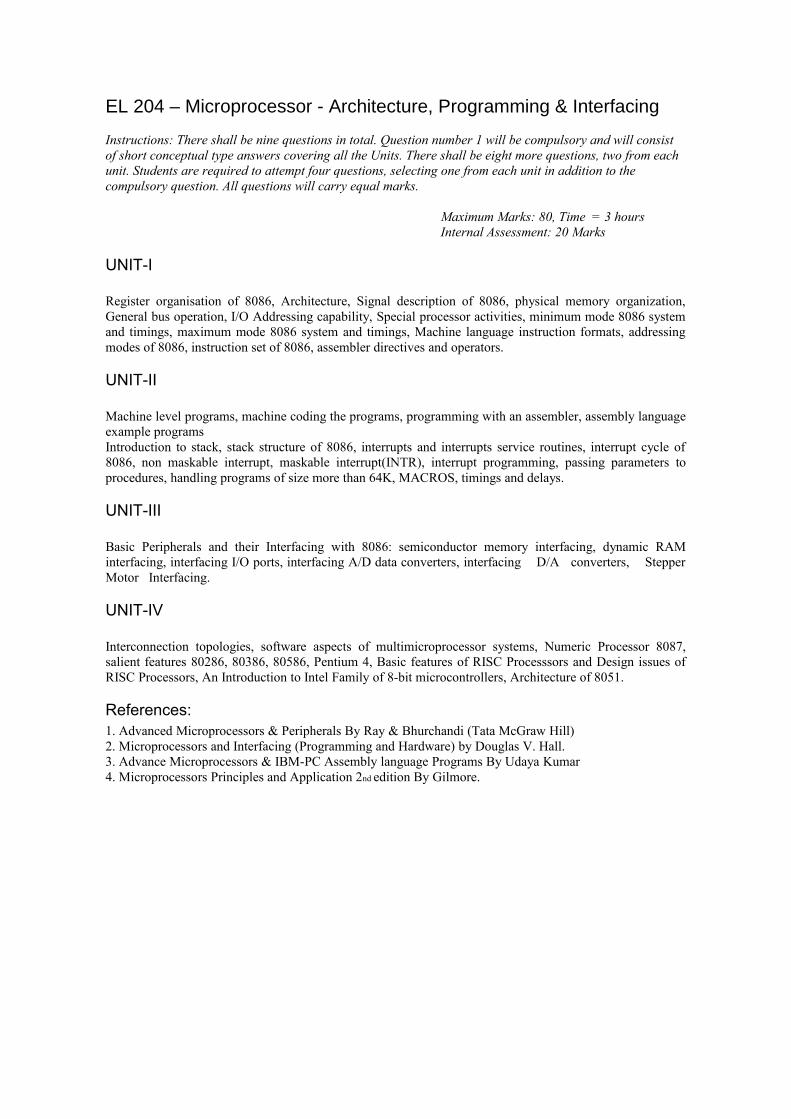
EL 204 – Microprocessor - Architecture, Programming & Interfacing
Instructions: There shall be nine questions in total. Question number 1 will be compulsory and will consist of short conceptual type answers covering all the Units. There shall be eight more questions, two from each unit. Students are required to attempt four questions, selecting one from each unit in addition to the compulsory question. All questions will carry equal marks.
Maximum Marks: 80, Time = 3 hoursInternal Assessment: 20 Marks
UNIT-I
Register organisation of 8086, Architecture, Signal description of 8086, physical memory organization, General bus operation, I/O Addressing capability, Special processor activities, minimum mode 8086 system and timings, maximum mode 8086 system and timings, Machine language instruction formats, addressing modes of 8086, instruction set of 8086, assembler directives and operators.
UNIT-II
Machine level programs, machine coding the programs, programming with an assembler, assembly language example programsIntroduction to stack, stack structure of 8086, interrupts and interrupts service routines, interrupt cycle of 8086, non maskable interrupt, maskable interrupt(INTR), interrupt programming, passing parameters to procedures, handling programs of size more than 64K, MACROS, timings and delays.
UNIT-III
Basic Peripherals and their Interfacing with 8086: semiconductor memory interfacing, dynamic RAM interfacing, interfacing I/O ports, interfacing A/D data converters, interfacing D/A converters, Stepper Motor Interfacing.
UNIT-IV
Interconnection topologies, software aspects of multimicroprocessor systems, Numeric Processor 8087, salient features 80286, 80386, 80586, Pentium 4, Basic features of RISC Processsors and Design issues of RISC Processors, An Introduction to Intel Family of 8-bit microcontrollers, Architecture of 8051.
References:1. Advanced Microprocessors & Peripherals By Ray & Bhurchandi (Tata McGraw Hill)2. Microprocessors and Interfacing (Programming and Hardware) by Douglas V. Hall.3. Advance Microprocessors & IBM-PC Assembly language Programs By Udaya Kumar4. Microprocessors Principles and Application 2nd edition By Gilmore.

EL205 Option(i) - MEMS and Microsystems: Fabrication, Design & Applications
Instructions: There shall be nine questions in total. Question number 1 will be compulsory and will consist of short conceptual type answers covering all the Units. There shall be eight more questions, two from each unit. Students are required to attempt four questions, selecting one from each unit in addition to the compulsory question. All questions will carry equal marks.
Maximum Marks: 80, Time = 3 hoursInternal Assessment: 20 Marks
Unit I
Overview of MEMS and Microsystems: Introduction Microsystem vs. MEMS, Microsystems and Microelectronics, the Multidisciplinary Nature of Microsystem design and manufacture, Application of MEMS in various industries.
MEMS and Miniaturization: Scaling laws in miniaturization: Introduction to Scaling, Scaling in: Geometry, Rigid Body dynamics, Elechoslatic forces, Electromagnetic forces, Electricity, Fluid Mechanics, Heat Transfer.
Unit II
Materials for MEMS and Microsystems – Si as substrate material, mechanical properties of Silicon, Silicon Compounds (SiO2, Si3N4, SiC, polySi, Silicon), Piezoresistors, GaAs, Piezoelectric crystals, Polymers, Packaging Materials.Micromachining Processes: Overview of microelectronic fabrication processes used in MEMS, Bulk Micromachining – Isotropic & Anisotropic Etching, Comparison of Wet vs Dry etching, Surface Micromachining – General description, Processing in general, Mechanical Problems associated with Surface Micromachining, Introduction to LIGA process, Introduction to Bonding.
Unit III
Microsystems & MEMS Design: Design Considerations: Design constraints, Selection of Materials, Selection of Manufacturing processes, Selection of Signal Transduction, Electromechanical system, packaging.
Process design, Mechanical Design – Thermo mechanical loading, Thermo mechanical Stress Analysis, Dynamic Analysis, Interfacial fracture Analysis, Mechanical Design using Finite Element Method, Computer Aided Design – Why CAD? Choice of a CAD Package, Design case using CAD.
Unit IV
Principles of Measuring Mechanical Quantities: Transduction from Deformation of Semiconductor Strain gauges: Piezoresistive effect in Single Crystal Silicon, Piezoresistive effect in Polysilicon Thin films, Transduction from deformation of Resistance. Capacitive Transduction: Electromechanics, Diaphragm pressure sensors.
Structure and Operation of Accelerometers, Resonant Sensors, Pressure sensors (Basics only)
References: 1. Microfabrication by Marc Madaon, CRC Press2. MEMS & Microsystems Design and Manufacture by Tai-Ran H Su, Tata Mcgraw3. Microsystem Design by S.D. Senturia, Ruiwer Academic Publisher4. Mechanical Mirosensors by M Elwenspock, R Wiegerink, Springer New York
EL205 Option(ii) – Nano Electronics - Materials & Devices
Instructions: There shall be nine questions in total. Question number 1 will be compulsory and will consist of short conceptual type answers covering all the Units. There shall be eight more questions, two from each unit. Students are required to attempt four questions, selecting one from each unit in addition to the compulsory question. All questions will carry equal marks.
Maximum Marks: 80, Time = 3 hoursInternal Assessment: 20 Marks
Unit I
Overview of progress of microelectronics worldwide. International technology roadmap characteristics. CMOS scaling. Nanoscale MOSFET, FinFET, vertical MOSFETS’s limits of CMOS technology. Materials & processes for advanced sub 65nm CMOD technology.
From microelectronics towards nanoelectronics. Noval approaches towards future devices. Introduction to nanotechnology and nanomaterials. Applications in different fields. Bottom up and top down approaches.
Unit II
Top Down Approaches:Semiconductor Low dimensional systems- Two dimensional confinement of carriers, Quantum wells, One dimensional Quantum systems; quantum wires, Zero dimensional quantum structures: Quantum Dots.Quantum devices: Res0onant tunneling diode & transistor. Coulomb Blockade, Single Electron Transistor, Introduction to Spintronics, Material requirements for spintronics, Spin devices: Spin Transistor, Spin values etc. Quantum computation.
Unit III
Bottom up Approaches:Molecular Electronics involving single molecules as electronic devices, chemical approaches to nanostructure materials. Band structures and transport in the molecular system. Molecular switches and logic gates. Molecular interconnects.Cabon nanotubes, structures and synthesis, growth mechanism and properties, devices applications. Nanowires:synthesis and characterization.
Unit IV
Nanofabrication: Thin film techniques, MBE, CVD, PECVD, Sol gel, Plasma arching electrodeposition, ball milling, atomic layer deposition, self assembly, template manufacturing, spray pyrolysis.Nanomanipulation and nano lithography: E-beam and nano imprint lithography, advanced nanolithography, High resolution nanolithography, Dip-Pen lithography, AFM Lithography.Nanocharacterization: High Reslution TEM, Scanning Probe Microscopes: Atomic Force Microscope and Scanning Tunneling Microscope, Photon Spectroscopy, Electron spectroscopy, Nano manipulator.
References:1. “Nanoelectronics and Information Technology”, (Advanced Electronic and Novel Devices), Waser
Ranier, Wiley- VCH (2003)2. “The Physics of Low-dimensional Semiconductors”. John H. Davies, Cambridge University Press,
1998.3. “Introduction to Nano Technology”, John Wiley & Sons, 2003.4. “Introduction to Molecular Electronics”, M.C. Petty, M.R.Bryce, and D.Bloor, Edward Arnold
(1995).5. “Quantum Hetrostructures”, V.Mitin, V. Kochelap, and M.Stroscio, Cambridge University Press.
EL 205 Option (iii) - Materials for VLSI
Instructions: There shall be nine questions in total. Question number 1 will be compulsory and will consist of short conceptual type answers covering all the Units. There shall be eight more questions, two from each unit. Students are required to attempt four questions, selecting on e from each unit in addition to the compulsory question. All questions will carry equal marks.
Maximum Marks: 80, Time = 3 hoursInternal Assessment: 20 Marks
Unit-I
Silicon Crystal growth and wafer preparations, starting materials, Metallurgical grade silicon, Polycrystalline Silicon, Single Crystal growth, Introduction, Float-Zone method, Czocharlski method, Impurities, impurity inhomogeneity, Wafer shaping process cleaning mechanical properties of the wafer.
Reference: Chapter 5, Chapter 8, Semiconductor Silicon Crystal Technology, Fumio Shimura, academic Press, Inc.
Unit-II
Silicon wafer criteria for VLSI/ULSI technology, High technology silicon wafer concept, VLSI/ULSI wafer characteristics, structural and chemical and mechanical characteristics, Deposited films. Polysilicon, Deposition variables, structure, Doping polysilicon, oxidation of polysilicon, properties of Polysilicon, Silicon dioxide, deposition methods, Deposition variable, Step coverage, p-glass flow, properties of silicon dioxide.
Reference:1. Chapter 5, Chapter 8, Semiconductor Silicon Crystal Technology, Fumio Shimura, Academic Press, Inc.2. Chapter 6, VLSI Technology, SM Szi, McGraw Hill International Ed.
Unit-III
Silicon nitride, nitride properties of silicon nitride, plasma-assisted deposition, deposition variable, properties of plasma assisted deposited filing, other material, materials for contacts and interconnects, Metallization, Applications, gates and interconnections, Ohmic contacts, Metallization choices, Metals or allays, properties, stability and semiconductor and insulating, patterning, Self-aligned silicides
Reference: Chapter 6, Chapter 9, VLSI Technology, S.M Sze, McGraw Hill International Ed.
Unit-IV
Metallization problem, deposition, processing, metallurgical and chemical interactions, electromigration, New role of metallization, multilevel structures, epitaxial metals, diffusion barriers and redundant metal links, Assembly and packaging of VLSI devices package types, packaging design considerations, thermal design considerations, electrical considerations, mechanical design considerations, VLSI assembly technologies, wafer preparation, die-banding, wire bonding, package fabrication technologies ceramic package, glass-sealed refractory package, plastic molding technology molding process, special package considerations.
Reference: Chapter 9, Chapter 13, VLSI Technology, S.M Sze, McGraw Hill International Ed.
EL 205 Option (iv) - Advanced Device Physics for VLSI
Instructions: There shall be nine questions in total. Question number 1 will be compulsory and will consist of short conceptual type answers covering all the Units. There shall be eight more questions, two from each unit. Students are required to attempt four questions, selecting on e from each unit in addition to the compulsory question. All questions will carry equal marks.
Maximum Marks: 80, Time = 3 hoursInternal Assessment: 20 Marks
Unit IMoore’s Law and Its Implications, Scaling of MOSFETs, Practical CMOS Scaling, Gate coupling velocity overshoot, high field effects, substrate current, hot carrier effects, Current CMOS Device Technology, International Technology Roadmap for Semiconductors (ITRS) Projections
Unit IINumerical simulation, Basic concepts of simulations, Device simulation, Simulation challenges. The Need for Semiconductor Device Modeling, Importance of Semiconductor Device Simulators, Key Elements of Physical Device Simulation, Historical Development of the Physical Device Modeling, Introduction to the Silvaco ATLAS Simulation Tool .
Unit III
The Scaling Limit of MOSFETs, New Materials ,Fully Depleted SOIDouble-Gate and Multiple-Gate FET Structures, Limits to Scaling, Power constrained scaling. Direct Source-Drain Tunneling EJ-MOSFETs, Concept of EJ-MOSFETs
Unit IVQuantum Effects in Silicon Nano-devices, Carrier Confinement in ThinSOI MOS Structures, Quantum effects on mobility and threshold voltage etc. Mobility and threshold voltage adjustment with quantum effects. Concept of ballistic transport, Resonant tunneling (RTD),Si based RTD devices, Concept of single electron transistor, Quantum well, quantum wire and quantum dot devices.
References:
a. Device electronics for integrated circuits - Muller & Kaminsb. Silicon Nanoelectronics - Shunri Oda & David Ferry, CRC Pressc. Computational Electronics - Dragica Vasileska and Stephen M. Goodnick,
Morgan & Claypool Publishers
EL 301 – MOS Solid State Circuits
Instructions: There shall be nine questions in total. Question number 1 will be compulsory and will consist of short conceptual type answers covering all the Units. There shall be eight more questions, two from each unit. Students are required to attempt four questions, selecting one from each unit in addition to the compulsory question. All questions will carry equal marks. Maximum Marks: 80, Time: 3 hours
Internal Assessment: 20 MarksUnit-IBasic digital building blocks, NMOS inverter and its sizing rules, single input NMOS NOR and NAND logic circuits, CMOS inverters, CMOS NOR logic gate, CMOS NAND logic gate, power dissipation , CMOS AND NMOS power dissipation, latch-up and its prevention, signal propagation delays, ratio-logic models, inverter pair delay, NMOS,NAND and NOR delays, CMOS logic delays. Unit-IIDynamic MOS storage circuits, dynamic charge storage, simple shift register, clocked CMOS logic, dynamic RAM memory, register storage circuits, datapath operators, bit-parallel adders, bit-serial adders, carry-save addition, pipelining, pipeline architecture, Floor planning methods, block placement and channel definition, routing, power distribution.
Unit-IIILayout Design rules, resistance estimation, capacitance estimation, MOS capacitor characteristics, MOS device capacitances, diffusion capacitances, single wire capacitance, capacitance design guide, inductance estimation, analytical delay models, gate delay model, power dissipation, static and dynamic power dissipation, short-circuit dissipation, total power dissipation.
Unit-IVCMOS tests methods, need for testing, functionality tests, manufacturing tests and principles, fault models, stuck-at faults, short-circuit and open-circuit faults, Automatic test pattern generation, geometrical specification languages, parameterized layout representation, graphical symbolic layout, layout equation symbology, design rule checks, digital circuit simulation, logic level simulation, switch level simulation, RTL level simulation.
References:1. VLSI Design Techniques for Analog and Digital Circuits by Randall L. Geiger, Phillip E. Allen and
Noel R. Strader, McGraw-Hill.2. Principles of CMOS VLSI Design- A System Perspective by Neil H.E. Weste and Kamrin
Eshraghin, Second Edition, Addison-Wesley.3. Modern VLSI design – System –on-Chip Design by Wayne Wolf, PHI, Third Edition.4. Fundamentals of Digital Logic Design by Pucknell (P.Hall)

EL 302 – Semiconductor Material & Device Characterisation
Instructions: There shall be nine questions in total. Question number 1 will be compulsory and will consist of short conceptual type answers covering all the Units. There shall be eight more questions, two from each unit. Students are required to attempt four questions, selecting one from each unit in addition to the compulsory question. All questions will carry equal marks. Maximum Marks: 80, Time: 3 hours
Internal Assessment: 20 MarksUnit-I
Resistivity measurement: Four point probe, Correction factors, Resistivity of arbitrarily shaped samples, Resistivity profiling: Anodic oxidation-four point probe, spreading resistance, contactless resistivity methods, conductivity type measurements.Carrier and doping concentration measurements: Capacitance measurements, Differential capacitance, Maximum-Minimum MOS-C capacitance, Integral capacitance.Current-Voltage measurements, Second harmonic, MOSFET substrate voltage-gate voltage, MOSFET threshold voltage.
Unit-II
Metal-Semiconductor Contacts: Contact resistance, Measurement techniques (introduction only), Hall effect and Mobility: Mobility, Conductivity mobility, Basic equations for uniform layers or wafers, Magnetoresistance mobility, MOSFET mobility: Effective mobility, field-effect mobility and Saturation mobility, Oxide and interface trapped charge: Characterization using Capacitance-Voltage curves only.
Unit-IIIDeep level Transient Spectroscopy: Conventional DLTS(only), Optical Microscopy: Resolution, Magnification, Contrast, Differential Interference Contrast, Defect etches, Ellipsometry: theory and applications, Transmission measurements: theory and instrumentation, Fourier Transform Infrared spectroscopy, Reflection Measurements, Line width measurements, Photoluminescence, Raman spectroscopy.
Unit-IVScanning Electron Microscopy, Auger Electron Spectroscopy, Electron Microprobe, Secondary Ion Mass Spectroscopy and X-ray Photoelectron Spectroscopy (Principle, instrumentation and its applications), Transmission Electron Microscopy, Electron Beam Induced Current, LEED and RHEED (idea only). Scanning Tunneling Microscope, Atomic Force Microscope (brief).
References:1. Semiconductor Material and Device Characterization-Dieter K.Schroder (John Wiley & Sons).2. Technique of Physics Vol.13, The Electrical Characterization of Semiconductors, Measurement of
Minority carrier Properties-J.W.Octon and P.Blood (Academic Press)3. VLSI Technology-S.M.Sze (McGraw Hill Publications).4. Nano – A Perspective – T.Pradeep (TMH)

EL 303 – Microwave & Optoelectronic Devices
Instructions: There shall be nine questions in total. Question number 1 will be compulsory and will consist of short conceptual type answers covering all the Units. There shall be eight more questions, two from each unit. Students are required to attempt four questions, selecting one from each unit in addition to the compulsory question. All questions will carry equal marks. Maximum Marks: 80, Time: 3 hours
Internal Assessment: 20 Marks
Unit IMicrowave Introduction, Waveguides, Rectangular Waveguides - excitation of modes, power transmission, power losses, Microwave parameters-cut off frequency, Characteristic Impedance, Attenuation constant, Phase, Reflection Coefficient, SWR, Power. Microwave passive components (brief)-discontinuities, bands, flanges, TEE’s, directional coupler, matched load, attenuators, phase shifter, transitions, ferrite components, slotted line, Wavemeter. Measurements of wavelength, Frequency, impedance, SWR etc. Rectangular Cavity Resonator, Q of cavity, Reentrant cavities. Conventional tubes-limitations at high frequencies, Klystron-operation, velocity modulation, bunching, output power, beam loading. Reflex Klystron-operation, velocity modulation, power output.
Unit IITraveling wave tube (in brief), Planar Triodes. Magnetrons (in brief).Transferred Electron Devices, Gunn Effect diode-operation, Modes of operation, microwave generation, amplification, Avalanche Transit Time Devices (in brief). - IMPATT diode, TRAPATT diode, BARITT diode. Parametric Devices & Parametric amplifiers (in brief),. Microwave field effect transistors-principles of operation, characteristics.
References:1. Microwave Devices and Circuits by Samuel Y. Liao (Prentice Hall India).2. Electronic Communication Systems by G. Kennedy (TMH).3. Microwave Engineering by R. Chatterjee.4. Microwave Semiconductor Devices and their Circuit Applications by H.A. Watson (McGraw Hill).
Unit IIIBasic principles of light emission in semiconductors, spontaneous emission, stimulated emission, lasing, lasing threshold, efficiency of light emission. Semiconductor lasers, the laser diode, basic structure, Optical modes, lasing threshold conditions, output power and efficiency. Heterostructure, basic heterostructure, laser structure, SH lasers, DH lasers, Performance characteristics of heterojunction lasers. Electro-luminescence, LED materials, LED construction, Response times of LED’s, LED’s structures for optical communication applications.
Unit IVDisplay devices, Luminescence, liquid crystal displays, Quantum well devices, Quantum wells and superlattices, Quantum well lasers, Junction detectors, Integrated Optical detectors, specialized photodiode structures, Techniques for modifying spectral response, factors limiting performance of integrated detectors. Optical fiber communication, Propagation in Fibers, step index fibers, graded index fibers, multipath dispersion, material dispersion combined effect, Attenuation in optical fibers, Semiconductors P-i-n photodiode detectors and Avalanche Photodiode Detectors for optical communication application, Optical fiber communication systems, OEIC.
References:1. Integrated Optics:Theory & Technology (3rd edition) by R.G. Hunsperger.2. Optoelectronics-An Introduction (2nd edition) by J. Wilson, J.F.B. Hawkes.3. Optical Communication Systems by John Gowar.

EL 304(option i) - Custom Microelectronics & ASICs
Instructions: There shall be nine questions in total. Question number 1 will be compulsory and will consist of short conceptual type answers covering all the Units. There shall be eight more questions, two from each unit. Students are required to attempt four questions, selecting one from each unit in addition to the compulsory question. All questions will carry equal marks.
Maximum Marks: 80, Time: 3 hoursInternal Assessment: 20 Marks
Unit-I
Microelectronics evolution, why custom microelectronics, Custom microelectronic techniques. Full hand crafted custom design, fixed cell architectures, soft cell architectures, macrocells, Analog cells, Gate array techniques, sea of gates, Routing considerations.
Unit-II
ASIC design flow, ASIC library design, Programmable ASIC’s, ASIC construction, physical design, CAD tools system partitioning, FPGA partitioning, partitioning methods.
Unit-III
Types of simulation, structural simulation, static timing analysis, Gate level simulation, Net capacitance, Logic systems, cell models, delay models static timing analysis, Formal verification, Switch level simulation, Transistor level simulation.
Unit-IV
Low level design entry, Schematic entry, Floor planning and placement, Floor planning goals and objectives placement terms and definitions, Goals and objectives physical design flow, Routing global routing, Detailed routing, Special routing, testing, Importance of testing, Boundary Scan test, Faults, Automatic test pattern generation, Built in self test, Simple test example.
Reference:1. Custom VLSI microelectronics-Stanley L.Hurst (Prentice hall International)2. Application-Specific Integrated circuit-Michael John Sebastian smith (Addison Wesley)3. Application-Specific Integrated characteristic (ASIC) Technology-Academic Press.
EL 304(option ii) - Embedded Systems
Instructions: There shall be nine questions in total. Question number 1 will be compulsory and will consist of short conceptual type answers covering all the Units. There shall be eight more questions, two from each unit. Students are required to attempt four questions, selecting one from each unit in addition to the compulsory question. All questions will carry equal marks.
Maximum Marks: 80, Time: 3 hoursInternal Assessment: 20 Marks
Unit-IEmbedded systems – introduction, role of processor and other hardware units, real-lifeexamples, embedded systems on chip, Introduction to CISC and RISC architecture. Structuralunits of processor, processor selection for embedded system, memory devices for embeddedsystems and allocation of memory, DMA, interfacing memory, processor and I/O devices, Timer and counting devices.
Unit II
Microcontrollers- survey, types, processor architecture, microcontroller memory types, microcontroller features,
Microcontroller 8051 Architecture :Hardware, I/o pins, ports and circuits, external memory, counters and timers
Unit III
Serial data Input/output, Interrupts8051 instruction set – data Move Instructions, Logical operations, Arithmatic operations, Jump and call Instructions, example programmes
Unit IV
An 8051 Microcontroller design: Specifications, a microcontroller design, testing the design, timing subroutines, Lookup tables, Serial data transmissionApplications : Keyboards, Displays, D/A and A/D Conversions
References
1. Embedded Systems Architecture, Programming and Design, by Raj Kamal, TMH, 2003.2. The 8051 Microcontroller by Kenneth J. Ayala, Penram International.3. Programming and Customizing 8051 Microcontroller by Myke Predko, Tata
McGraw Hill.

EL 304(option iii) - Digital Signal Processing in VLSI
Instructions: There shall be nine questions in total. Question number 1 will be compulsory and will consist of short conceptual type answers covering all the Units. There shall be eight more questions, two from each unit. Students are required to attempt four questions, selecting one from each unit in addition to the compulsory question. All questions will carry equal marks.
Maximum Marks: 80, Time: 3 hoursInternal Assessment: 20 Marks
Unit-I
Introduction, Review of signals and signals processing, Enhancement of S/N, system models and the transfer function, spectra, limitations of Analog systems.Digital Signal Processing: Flexibility, key advantage to DSP, DSP issues and terminology, Sampled Data, Throughput expansion, data compression and pipelining.Non-recursive filters: Finite impulse response filters; Digital filtersRecursive filters: Analog feedback filters and their recursive digital counterparts, Digital filter in block diagram form.
Unit-II
Digital Filter Overview: Digital filters, when, why, what, how? Comparison of digital filter types; summary of key digital filter relationships.FIR filters: FIR filter concepts and properties, Fourier-series approach to FIR filters; The window method of FIR filter design.FIR Filters: The second-order section as a prototype; Biquads for special purposes; Hardware implementation of FIR filters.The bridge to VLSI: Introduction, Some VLSI-DSP design Philosophy DSP, Architecture Issues: Tradeoffs, Pipelining, and parallelism,
Unit-III
Finite-word length arithmetic-Introduction, Arithmetic error sensitivity, Overflow, underflow, and rounding; filter quantization-error trade offs in fixed-point arithmetic, Accuracy in FFT spectral Analysis.
Analog I/O methods
Real DSP Hardware: Introduction, key, DSP hardware elements, System Selection: DSP system alternatives; Microcoded systems; Single-chip DSP microprocessor survey.
Unit-IV
DSP applications: Introduction, Major elements of a DSP system, the digital Transceiver; Digital detection, Digital heterodyning, decimation and interpolation.Real-time detection: Examples based on correlation principles, coherent detectionModeling in Real time: Telecommunications and speech. Why modeling; Telecommunications; coding of speech.Image Processing: Introduction to image processing; Machine vision acquisition, enhancement, and recognition.
Reference: Digital Signal Processing in VLSI by Richard J.Higgins(Prentice Hall)

EL 305(option i) – Digital Communication
Instructions: There shall be nine questions in total. Question number 1 will be compulsory and will consist of short conceptual type answers covering all the Units. There shall be eight more questions, two from each unit. Students are required to attempt four questions, selecting one from each unit in addition to the compulsory question. All questions will carry equal marks.
Maximum Marks: 80, Time: 3 hoursInternal Assessment: 20 Marks
Unit IModel Communication System, Elements of Digital Communication systems, Analysis and Design ofcommunication system, classification of signals and systems, system response and filters, spectral analysisof modulation and demodulation operations.Random Signal Theory:Probabilities, and Random variablesInformation and channel Capacity:Measure of Information, Encoding of Source output, communicationchannels, discrete communication channels, continuouschannels.
Unit IIBaseband Data Transmission:Baseband Binary PAM systems, Duobinary Baseband PAM systems, M-arysignalling schemes, Digital carrier.Modulation Schemes:Binary ASK, PSK, FSK schemes, Comparison of Digital Modulation Schemes.
Unit IIIError control coding:Examples of Error control coding, Methods of controlling errors, Types of errorsandcodes, Linear block codes, Binary cyclic codes.
Unit IVDigital Transmission of Analog Signals, Sampling theory and Practice, Quantizing of Analog Signals,codesTransmission of analog signals, PCM, Delta Modulation, Q-level differential PCM, Time DivisionMultiplexing, comparison of Method of analog signal transmission.
References:1. Digital and Analog Communication Systems by K. Sam Shanmugan (John wiley & Sons 1994).2. Principles of Communication System by Taub and Schilling (McGraw Hill International).3. An Introduction to Analog & Digital Communication by Sinon Haykin.4. Principles of Digital and Analog communications by Jerry D. Gibsons, Maxwell (Macmillian
Internation Editions).5. Digital and Analog communication Systems by Leon W. Couch, Maxwell (Macmillian
International Edition).

EL 305 (option ii) - Optical Fiber Communication
Instructions: There shall be nine questions in total. Question number 1 will be compulsory and will consist of short conceptual type answers covering all the Units. There shall be eight more questions, two from each unit. Students are required to attempt four questions, selecting one from each unit in addition to the compulsory question. All questions will carry equal marks.
Maximum Marks: 80, Time: 3 hoursInternal Assessment: 20 Marks
Unit-IOptical communication, Introduction, the measurement of information & capacity of a telecommunication channel, communication system architecture, the basic communication system, Optical communication system, the economic merits, optical fibers digital telecommunication system, analogue system, application & future developments, optical satellite communication.
Unit-IIElementary discussion of propagation in Fibers, Propagation a ray model, signal degradation in optical fibers, Material dispersion, the combined effect of material dispersion & multipath dispersion, RMS pulse widths & frequency response, attenuation in optical fibers, attenuation mechanisms, assessment of silica fibers & cables, power launching and coupling, fiber connectors, splices & couples.
Unit-IIISemiconductor lasers for optical communication, the development of stripe geometry lasers, direct modulation of S.C.lasers, optical & electrical characterization of stripe geometry & buried heterostructure lasers, sources for longer wavelength LED’s efficiency of DHLED. LED structures, characteristics, reliability, modulation (AM, FM & pulse modulation).
Unit-IVOptical fiber systems, intensity modulation/direct detection, the optical transmitter circuit, the optical receiver circuit, system design consideration, digital systems, planning consideration, analog system, coherent optical fiber system, detection principles, practical constraints, modulation formats, Demodulation schemes, receiver sensitivities, optical fiber communication application & future developments (Public, Military, Industrial & Computer) application, local area networks.
References:1. Optical fiber communications (Principle and Practice) 2nd edition-John M.Senior (Prentice Hall India
Pvt. Ltd, New Delhi).2. Optical Communication Systems Second edition-John Gowar (Prentice Hall India Pvt. Ltd, New Delhi).3. Optical Fiber Communications-Gerd Keiser (McGraw Hill International editions, Singapore).
Additional References:1. Fundamental of optical fiber communication second edition-Michael K.Barnoski (Academic Press,
Orlando).2. Fiber Optic Communication Systems-Govind P.Agarwal (John Wiley & Sons, Singapore).3. Integrated Optics: Theory & Technology third edition-R.G. Hunsperger-Springer Series in Optical
Sciences Series (Springer-Verlag, Berlin).4. Telecommunications-Voice/Data with Fiber Optic Applications-Wayne Tomasi & Vincent T.
Alisouskas (Prentice Hall International edition)5. Optical FIBER Systems: Technology, Design and Applications-Charles K.Kao.

EL 305 option (iii) - RF MicroelectronicsInstructions: There shall be nine questions in total. Question number 1 will be compulsory and will consist of short conceptual type answers covering all the Units. There shall be eight more questions, two from each unit. Students are required to attempt four questions, selecting one from each unit in addition to the compulsory question. All questions will carry equal marks.
Maximum Marks: 80, Time: 3 hoursInternal Assessment: 20 Marks
Unit-IImportance of RF and wireless technology, IC design technology for RF circuitsRF Behavior of passive components, operation for passive components at RFActive RF Components, RF Diodes, RF BJTs, RF FET, HEMT Active RF component modelling, Transistor models, Unit-IICircuit representation of two port RF / Microwave Networks, Low and high frequencyparameters, Formulation and properties of s parameters, Shifting reference plans,Transmission matrix, Generalized scattering parameters, Passive Circuit design, Review of Smith chart Matching and Biasing networks, Impedence matching using discrete components, microstrip line matching networks, amplifier classes of operation, RF Transistor amplifier designs, Low Noise amplifiers, Stability consideration, Constant gain noise figure circles
Unit-IIINoise considerations in active networks, Noise definition, noise sources .RF / Microwave oscillator design, Oscillator versus amplifier design, Oscillation conditions, Design of transistor oscillators, Generator Tuning networksRF / Microwave Frequency conversion II : Mixer design, Mixer types, Conversion loss for SSB mixers, SSB mixer versus DSB mixers. One diode mixers, Two diode mixers, Four diode mixers, Eight diode mixers,
Unit-IVFrequency synthesizers, PLL, RF synthesizer architectures, Transceiver architectures, Receiver architectures, Transmitter architectures, RF / Microwave IC design, Microwave ICs, MIC Materials, Types of MICs, Hybrid vs monolithic MICs, Case studies, Relating to design of different circuits employed in RF Microelectronics
References1. Behzad Razavi, “RF Microelectronics” Prentice Hall PTR , 19982. R.Ludwig, P.Bretchko, RF Circuit Design, Pearson Education Asia, 2000.3. Matthew M. Radmanesh, Radio Frequency and Microwave Electronics Illustrated, Pearson
Education (Asia) Ltd., 2001