Embed Size (px)
Citation preview

4.096 V
ADS886016-Bit SAR
1 MSPS
REF5040
LM7705
OPA837
2.2 nF
3.3 VGND
GNDGND
GND
PD0 V 3.8 V
Gain = 1.05 V/V
0 V 4.0 V
+ 5.0 V
± 0.23 V+ 3.3 V
22 �
22 �
499 �
10.0 k�
+
±
+VCC
±VCC
Product
Folder
Order
Now
Technical
Documents
Tools &
Software
Support &Community
ReferenceDesign
An IMPORTANT NOTICE at the end of this data sheet addresses availability, warranty, changes, use in safety-critical applications,intellectual property matters and other important disclaimers. PRODUCTION DATA.
OPA837, OPA2837SBOS673A –SEPTEMBER 2017–REVISED APRIL 2018
OPAx837 Low-Power, Precision, 105-MHz, Voltage-Feedback Op Amp
1
1 Features1• Bandwidth: 105 MHz (AV = 1 V/V)• Very Low (Trimmed) Supply Current: 600 µA• Gain Bandwidth Product: 50 MHz• Slew Rate: 105 V/µs• Negative Rail Input, Rail-to-Rail Output• Single-Supply Operating Range: 2.7 V to 5.4 V• 25°C Input Offset: ±130 µV (Max)• Input Offset Voltage Drift (DCK Package):
< ±1.6 µV/°C (Maximum)• Input Voltage Noise: 4.7 nV/√Hz (> 100 Hz)• HD2: –120 dBc at 2 VPP, 100 kHz• HD3: –145 dBc at 2 VPP, 100 kHz• Settling Time: 35 ns, 0.5-V Step to 0.1%• 5-µA Shutdown Current With Fast Recovery From
Shutdown for Power Scaling Applications
2 Applications• 12-Bit to 16-Bit, Low-Power SAR Drivers• Precision ADC Reference Buffers• Very-Low-Power Active Filters• Low-Power Transimpedance Amplifiers• Sensor Signal Conditioning• Wearable Devices• Low-Side Current Sensing
Low-Power, Low-Noise, Precision, Single-EndedSAR ADC Driver With True Ground Input and
Output Range
3 DescriptionThe OPA837 and OPA2837 are single- and dual-channel unity-gain stable, voltage-feedback amplifiersthat provide among the highest MHz per mW ofbandwidth versus power among precision op amps.Using only 600 µA per channel on a single 5-Vsupply, these 3.0-mW devices deliver 105-MHzbandwidth at a gain of 1 V/V. The very low trimmedoffset voltage of ±130 µV (maximum) comes with atypical (±1σ) drift of ±0.4 µV/°C.
Ideally suited to single-ended, successive-approximation register (SAR) analog-to-digital-converter (ADC) driving applications, the OPAx837provides one of the lowest input spot noise levels at4.7 nV/√Hz for the 3-mW quiescent power. The veryhigh 50-MHz gain bandwidth product provides the lowoutput impedance to high frequencies required tosupply the fast charging currents in SAR ADC driverapplications. This low dynamic output impedance isalso suitable for reference buffer applications withprecision ADCs. The single-channel OPA837 isavailable in a 6-pin SOT-23 package (that includes apower shutdown feature) and a 5-pin SC70 packagewhereas the dual-channel OPA2837 is available in an8-pin VSSOP package.
The OPAx837 is characterized for operation over thea wide temperature range of –40°C to +125°C.
Device Information(1)
PART NUMBER PACKAGE BODY SIZE (NOM)
OPA837SOT-23 (6) 2.90 mm × 1.60 mmSC70 (5) 2.00 mm × 1.25 mm
OPA2837 VSSOP (8) 3.00 mm × 3.00 mm
(1) For all available packages, see the package option addendumat the end of the data sheet.

2
OPA837, OPA2837SBOS673A –SEPTEMBER 2017–REVISED APRIL 2018 www.ti.com
Product Folder Links: OPA837 OPA2837
Submit Documentation Feedback Copyright © 2017–2018, Texas Instruments Incorporated
Table of Contents1 Features .................................................................. 12 Applications ........................................................... 13 Description ............................................................. 14 Revision History..................................................... 25 Pin Configuration and Functions ......................... 36 Specifications......................................................... 4
6.1 Absolute Maximum Ratings ...................................... 46.2 ESD Ratings.............................................................. 46.3 Recommended Operating Conditions....................... 46.4 Thermal Information: OPA837 .................................. 56.5 Thermal Information: OPA2837 ................................ 56.6 Electrical Characteristics: VS = 5 V........................... 66.7 Electrical Characteristics: VS = 3 V........................... 86.8 Typical Characteristics: VS = 5.0 V......................... 106.9 Typical Characteristics: VS = 3.0 V......................... 136.10 Typical Characteristics: ±2.5-V to ±1.5-V Split
Supply ...................................................................... 167 Detailed Description ............................................ 21
7.1 Overview ................................................................. 217.2 Functional Block Diagrams ..................................... 21
7.3 Feature Description................................................. 227.4 Device Functional Modes........................................ 25
8 Application and Implementation ........................ 298.1 Application Information............................................ 298.2 Typical Applications ................................................ 38
9 Power Supply Recommendations ...................... 4210 Layout................................................................... 42
10.1 Layout Guidelines ................................................. 4210.2 Layout Example .................................................... 43
11 Device and Documentation Support ................. 4411.1 Documentation Support ........................................ 4411.2 Related Links ........................................................ 4411.3 Receiving Notification of Documentation Updates 4411.4 Community Resources.......................................... 4411.5 Trademarks ........................................................... 4411.6 Electrostatic Discharge Caution............................ 4411.7 Glossary ................................................................ 45
12 Mechanical, Packaging, and OrderableInformation ........................................................... 45
4 Revision History
Changes from Original (September 2017) to Revision A Page
• Added OPA2837 to document ............................................................................................................................................... 1• Added Single-Supply Operating Range Features bullet......................................................................................................... 1• Changed 1 SPS to 1 MSPS in front page figure ................................................................................................................... 1• Added footnote to Pin Functions table .................................................................................................................................. 3• Changed footnote describing method of computation of slew rate in Electrical Characteristics: VS = 5 V table ................... 6• Changed default test condition in Electrical Characteristics: VS = 3 V table ......................................................................... 8• Changed footnote describing method of computation of slew rate in Electrical Characteristics: VS = 3 V table .................. 8• Changed values for common-mode input range, high in Electrical Characteristics: VS = 3 V table ...................................... 9• Changed values for VOH in Electrical Characteristics: VS = 3 V table .................................................................................... 9• Changed VO = 20 mVPP to VOUT = 200 mVPP in conditions of Noninverting Response Flatness vs Gain and Inverting
Response Flatness vs Gain figures...................................................................................................................................... 10• Changed gain –1 V/V to gain –2 V/V, swapped legend colors in Inverting Overdrive Recovery figure............................... 11• Changed VOUT = 2 VPP to VOUT = 1 VPP in conditions of Typical Characteristics: VS = 3.0 V section ................................... 13• Changed VO = 20 mVPP to VOUT = 200 mVPP in Noninverting Response Flatness vs Gain and Inverting Response
Flatness vs Gain figure conditions........................................................................................................................................ 13• Changed VIN to VIN × –1 gain, swapped legend colors in Inverting Overdrive Recovery figure .......................................... 14• Changed VO = 2 VPP to VOUT = 1 VPP in Harmonic Distortion vs RLOAD figure conditions..................................................... 15• Changed VOUT = 2 VPP to VOUT = 1 VPP in Harmonic Distortion vs Gain Magnitude figure conditions ................................. 15• Changed y-axis caption in Turn-On Time to Sinusoidal Input and Turn-Off Time to Sinusoidal Input figures..................... 18• Added OPA838 row to Device Family Comparison table..................................................................................................... 22• Changed EVM link in Split-Supply Operation section from OPA837DBV to OPA835DBV .................................................. 25• Changed V2 value from 2.5 to –2.5 V in Characterization Test Circuit for Network, Spectrum Analyzer figure ................. 29• Changed VEE value from 2.5 V to –2.5 V in Inverting Characterization Circuit for Network Analyzer figure ....................... 31• Changed 1 SPS to 1 MSPS in OPA837 and ADS8860 Example Circuit figure................................................................... 37

VS+
VS-
1
2
3
4 5
6
7
8
VIN1-
VIN1+ VIN2-
VIN2+
VOUT1
VOUT2
A
B
1
2
3
5
4
VS+
VIN-
VOUT
VS-
VIN+
1
2
3
6
5
4
VS+
PD
VIN-
VOUT
VS-
+IN
3
OPA837, OPA2837www.ti.com SBOS673A –SEPTEMBER 2017–REVISED APRIL 2018
Product Folder Links: OPA837 OPA2837
Submit Documentation FeedbackCopyright © 2017–2018, Texas Instruments Incorporated
5 Pin Configuration and Functions
OPA837 DBV Package6-Pin SOT-23
Top View
OPA837 DCK Package5-Pin SC70Top View
OPA2837 DGK Package8-Pin VSSOP
Top View
(1) I = input, O = output, and P = power.
Pin FunctionsPIN
FUNCTION (1) DESCRIPTIONNAME
OPA837 OPA2837SOT-23 SC-70 VSSOP
PD 5 — — I Amplifier power down.Low = disabled, high = normal operation (pin must be driven).
VIN– 4 4 — I Inverting input pinVIN+ 3 3 — I Noninverting input pinVIN1– — — 2 I Amplifier 1 inverting input pinVIN1+ — — 3 I Amplifier 1 noninverting input pinVIN2– — — 6 I Amplifier 2 inverting input pinVIN2+ — — 5 I Amplifier 2 noninverting input pinVOUT 1 1 — O Output pinVOUT1 — — 1 O Amplifier 1 output pinVOUT2 — — 7 O Amplifier 2 output pinVS– 2 2 4 P Negative power-supply pinVS+ 6 5 8 P Positive power-supply input

4
OPA837, OPA2837SBOS673A –SEPTEMBER 2017–REVISED APRIL 2018 www.ti.com
Product Folder Links: OPA837 OPA2837
Submit Documentation Feedback Copyright © 2017–2018, Texas Instruments Incorporated
(1) Stresses beyond those listed under Absolute Maximum Ratings may cause permanent damage to the device. These are stress ratingsonly, which do not imply functional operation of the device at these or any other conditions beyond those indicated under RecommendedOperating Conditions. Exposure to absolute-maximum-rated conditions for extended periods may affect device reliability.
(2) Staying below this ± supply turn-on edge rate prevents the edge-triggered ESD absorption device across the supply pins from turningon.
(3) Long-term continuous output current for electromigration limits.
6 Specifications
6.1 Absolute Maximum Ratingsover operating free-air temperature range (unless otherwise noted) (1)
MIN MAX UNIT
VS– to VS+Supply voltage 5.5 VSupply turn-on/off maximum dV/dT (2) 1 V/µs
VI Input voltage VS– – 0.5 VS+ + 0.5 VVID Differential input voltage ±1 VII Continuous input current ±10 mAIO Continuous output current (3) ±20 mA
Continuous power dissipation See Thermal Information:OPA837
TJ Maximum junction temperature 150 °CTA Operating free-air temperature –40 125 °CTstg Storage temperature –65 150 °C
(1) JEDEC document JEP155 states that 500-V HBM allows safe manufacturing with a standard ESD control process.(2) JEDEC document JEP157 states that 250-V CDM allows safe manufacturing with a standard ESD control process.
6.2 ESD RatingsVALUE UNIT
V(ESD) Electrostatic dischargeHuman body model (HBM), per ANSI/ESDA/JEDEC JS-001 (1) ±1500
VCharged-device model (CDM), per JEDEC specification JESD22-C101 (2) ±1000
6.3 Recommended Operating Conditionsover operating free-air temperature range (unless otherwise noted)
MIN NOM MAX UNITVS+ Single-supply voltage 2.7 5 5.4 VTA Ambient temperature –40 25 125 °C

5
OPA837, OPA2837www.ti.com SBOS673A –SEPTEMBER 2017–REVISED APRIL 2018
Product Folder Links: OPA837 OPA2837
Submit Documentation FeedbackCopyright © 2017–2018, Texas Instruments Incorporated
(1) For more information about traditional and new thermal metrics, see the Semiconductor and IC Package Thermal Metrics applicationreport.
6.4 Thermal Information: OPA837
THERMAL METRIC (1)
OPA837
UNITDBV(SOT23-6)
DCK(SC70)
6 PINS 5 PINS
RθJA Junction-to-ambient thermal resistance 194 203 °C/W
RθJCtop Junction-to-case (top) thermal resistance 129 152 °C/W
RθJB Junction-to-board thermal resistance 39 76 °C/W
ψJT Junction-to-top characterization parameter 26 58 °C/W
ψJB Junction-to-board characterization parameter 39 76 °C/W
(1) For more information about traditional and new thermal metrics, see the Semiconductor and IC Package Thermal Metrics applicationreport.
6.5 Thermal Information: OPA2837
THERMAL METRIC (1)
OPA2837
UNITDGK(VSSOP-8)
8 PINS
RθJA Junction-to-ambient thermal resistance 182 °C/W
RθJCtop Junction-to-case (top) thermal resistance 63.5 °C/W
RθJB Junction-to-board thermal resistance 103.6 °C/W
ψJT Junction-to-top characterization parameter 7.9 °C/W
ψJB Junction-to-board characterization parameter 101.8 °C/W

6
OPA837, OPA2837SBOS673A –SEPTEMBER 2017–REVISED APRIL 2018 www.ti.com
Product Folder Links: OPA837 OPA2837
Submit Documentation Feedback Copyright © 2017–2018, Texas Instruments Incorporated
(1) Test levels (all values set by characterization and simulation): (A) 100% tested at 25°C, overtemperature limits by characterization andsimulation; (B) Not tested in production, limits set by characterization and simulation; (C) Typical value only for information.
(2) This slew rate is the average of the rising and falling time estimated from the large-signal bandwidth as: (0.8 × VPEAK / √2) × 2π × f–3dBwhere this f–3dB is the typical measured 2-VPP bandwidth at gains of 1 V/V.
(3) Input offset voltage drift, input bias current drift, and input offset current drift are average values calculated by taking data at the endpoints, computing the difference, and dividing by the temperature range. Typical drift specifications are ±1sigma. Maximum driftspecifications are set by min/max sample packaged test data using a wafer-level screened drift. Min/Max drift is not specified by finalautomated test equipment (ATE) nor by QA sample testing.
(4) Current is considered positive out of the pin.
6.6 Electrical Characteristics: VS = 5 Vat VS+ = 5 V, VS– = 0 V, RF = 0 Ω, RL = 2 kΩ, G = 1 V/V, input and output referenced to mid-supply, and TA ≈ 25°C (unlessotherwise noted)
PARAMETER TEST CONDITIONS MIN TYP MAX UNIT TESTLEVEL (1)
AC PERFORMANCE
SSBW Small-signal bandwidth
VOUT = 20 mVPP, G = 1 90 105
MHz
C
VOUT = 20 mVPP, G = 2 45 C
VOUT = 20 mVPP, G = 10 5 C
GBP Gain-bandwidth product VOUT = 20 mVPP, G = 10 45 50 MHz C
LSBW Large-signal bandwidth VOUT = 2 VPP, G = 2 26 MHz C
Bandwidth for 0.1-dB flatness VOUT = 200 mVPP, G = 2 6 MHz C
SR Slew rate From LSBW (2) 105 V/µs C
tR, tF Rise, fall time VOUT = 0.5-V step, G = 2, input tR = 10 ns 10 11 ns C
Overshoot VOUT = 2-V step, G = 2, input tR = 40 ns 7.0% C
Settling time to 0.1% VOUT = 2.0-V step, G = 1, input tR = 4 ns 25 ns C
Settling time to 0.01% VOUT = 2.0-V step, G = 1, input tR = 4 ns 40 ns C
HD2 Second-order harmonic distortion f = 100 kHz, VO = 2 VPP, G = 1 (see Figure 73) –120 dBc C
HD3 Third-order harmonic distortion f = 100 kHz, VO = 2 VPP, G = 1 (see Figure 73) –145 dBc C
Input voltage noise f = 500 Hz 4.7 nV/√Hz C
Voltage noise 1/f corner frequency See Figure 39 35 Hz C
Input current noise f = 20 kHz 0.4 pA/√Hz C
Current noise 1/f corner frequency See Figure 39 5 kHz C
Overdrive recovery time G = 2, 2x output overdrive (see Figure 30) 75 ns C
Closed-loop output impedance f = 1 MHz, G = 1 (see Figure 38) 0.14 Ω C
Channel-to-channel crosstalk(OPA2837) f = 10 kHz -126 dBc C
DC PERFORMANCE
AOL Open-loop voltage gain VO = ±2 V, RL = 2 kΩ 120 135 dB A
Input-referred offset voltage
TA ≈ 25°C –130 ±30 130
µV
A
TA = 0°C to +70°C (DCK package) –170 ±30 200 B
TA = –40°C to +85°C (DCK package) –234 ±30 226 B
TA = –40°C to +125°C (DCK package) –234 ±30 290 B
Input offset voltage drift (3)
DCK package, TA = –40°C to +125°C –1.6 ±0.4 1.6
µV/°C
B
DBV package, TA = –40°C to +125°C –2.0 ±0.4 2.0 B
OPA2837, TA = –40°C to +125°C ±0.67 B
Input bias current (4)
TA ≈ 25°C 150 340 520
nA
A
TA = 0°C to +70°C 50 340 664 B
TA = –40°C to +85°C 50 340 718 B
TA = –40°C to +125°C 50 340 850 B
Input bias current drift (3) TA = –40°C to +125°C 0.8 1.5 3.3 nA/°C B
Input offset current
TA ≈ 25°C (OPA837) –40 ±6 40
nA
A
TA = 0°C to +70°C –46 ±6 52 B
TA = –40°C to +85°C –56 ±6 55 B
TA = –40°C to +125°C –56 ±6 65 B
TA ≈ 25°C (OPA2837) -60 ±8 60 A

7
OPA837, OPA2837www.ti.com SBOS673A –SEPTEMBER 2017–REVISED APRIL 2018
Product Folder Links: OPA837 OPA2837
Submit Documentation FeedbackCopyright © 2017–2018, Texas Instruments Incorporated
Electrical Characteristics: VS = 5 V (continued)at VS+ = 5 V, VS– = 0 V, RF = 0 Ω, RL = 2 kΩ, G = 1 V/V, input and output referenced to mid-supply, and TA ≈ 25°C (unlessotherwise noted)
PARAMETER TEST CONDITIONS MIN TYP MAX UNIT TESTLEVEL (1)
(5) The typical specification is at 25°C TJ. The min, max limits are expanded for the automated test equipment (ATE) to account for anambient range from 22°C to 32°C with a 2-µA/°C temperature coefficient on the supply current.
Input offset current drift (3) TA = –40°C to +125°C –250 ±40 250pA/°C
B
TA = –40°C to +125°C (OPA2837) –270 ±80 250 B
Input-referred offset voltagemismatch TA ≈ 25°C (OPA2837) -220 50 220 µV A
INPUT
Common-mode input range, lowTA ≈ 25°C, < 3-dB degradation in CMRR limit –0.2 0
VA
TA = –40°C to +125°C, < 3-dB degradation inCMRR limit –0.2 0 B
Common-mode input range, highTA ≈ 25°C, < 3-dB degradation in CMRR limit 3.7 3.8
VA
TA = –40°C to +125°C, < 3-dB degradation inCMRR limit 3.7 3.8 B
CMRR Common-mode rejection ratio 95 110 dB A
Input impedance common-mode 250 || 1.5kΩ || pF
C
Input impedance differential mode 180 || 0.5 C
OUTPUT
VOL Output voltage, lowTA ≈ 25°C, G = 2 0.05 0.1
VA
TA = –40°C to +125°C, G = 5 0.05 0.1 B
VOH Output voltage, highTA ≈ 25°C, G = 2 4.9 4.95
VA
TA = –40°C to +125°C, G = 5 4.8 4.9 B
Maximum current into a resistiveload TA ≈ 25°C, ±1.6 V into 27 Ω, VIO < 2 mV ±58 ±70 mA A
Linear current into a resistive load TA ≈ 25°C, ±1.7 V into 37.4 Ω, AOL > 80 dB ±45 ±50 mA A
Linear current into a resistive loadovertemperature
TA = –40°C to +125°C, ±1.31 V into 37.4 Ω,AOL > 80 dB ±35 ±45 mA C
Closed-loop output impedance Gain of 1 V/V, ±30-mA DC 0.6 mΩ C
POWER SUPPLY
Specified operating voltage 2.7 5.4 V B
Quiescent operating current peramplifier (5-V supply)
TA ≈ 25°C (5) 564 592 625µA
A
TA = –40°C to +125°C 408 592 865 B
Supply current temperaturecoefficient per amplifier TA = –40°C to +125°C (see Figure 57) 1.1 1.9 2.4 µA/°C B
+PSRR Positive power-supply rejectionratio 95 110 dB A
–PSRR Negative power-supply rejectionratio 92 108 dB A
POWER DOWN (Pin Must be Driven)
Enable voltage threshold Specified on above VS– + 1.5 V 1.5 V A
Disable voltage threshold Specified off below VS– + 0.55 V 0.55 V A
Power-down pin bias current PD = 0 V to VS+ –50 50 nA A
Power-down quiescent current PD ≤ 0.55 V 4 5 10 µA A
Power-down quiescent currentover temperature PD ≤ 0.55 V, TA = –40°C to +125°C 10 µA B
Turnon time delay Time from PD = high to VOUT = 90% of finalvalue 300 ns C
Turnoff time delay Time from PD = low to VOUT = 10% of originalvalue 100 ns C

8
OPA837, OPA2837SBOS673A –SEPTEMBER 2017–REVISED APRIL 2018 www.ti.com
Product Folder Links: OPA837 OPA2837
Submit Documentation Feedback Copyright © 2017–2018, Texas Instruments Incorporated
(1) Test levels (all values set by characterization and simulation): (A) 100% tested at 25°C, overtemperature limits by characterization andsimulation; (B) Not tested in production, limits set by characterization and simulation; (C) Typical value only for information.
(2) This slew rate is the average of the rising and falling time estimated from the large-signal bandwidth as: (0.8 x VPEAK / √2) × 2π × f–3dBwhere this f-3dB is the typical measured 2-Vpp bandwidth at gains of 1V/V.
(3) Input offset voltage drift, input bias current drift, and input offset current drift are average values calculated by taking data at the endpoints, computing the difference, and dividing by the temperature range. Typical drift specifications are ±1sigma. Maximum driftspecifications are set by min/max sample packaged test data using a wafer-level screened drift. Min/Max drift is not specified by finalautomated test equipment (ATE) nor by QA sample testing.
(4) Current is considered positive out of the pin.
6.7 Electrical Characteristics: VS = 3 Vat VS+ = 3 V, VS– = 0 V, RF = 0 Ω, RL = 2 kΩ, G = 1 V/V, input and output referenced to mid-supply, and TA ≈ 25°C (unlessotherwise noted)
PARAMETER TEST CONDITIONS MIN TYP MAX UNIT TESTLEVEL (1)
AC PERFORMANCE
SSBW Small-signal bandwidth
VOUT = 20 mVPP, G = 1 85 105
MHz
C
VOUT = 20 mVPP, G = 2 45 C
VOUT = 20 mVPP, G = 10 5 C
GBP Gain-bandwidth product VOUT = 20 mVPP, G = 10 40 50 MHz C
LSBW Large-signal bandwidth VOUT = 1 VPP, G = 2 30 MHz C
Bandwidth for 0.1-dB flatness VOUT = 200 mVPP, G = 2 6 MHz C
SR Slew rate From LSBW (2) 65 V/µs C
tR, tF Rise, fall time VOUT = 0.5-V step, G = 2, input tR = 10 ns 10 11 ns C
Overshoot VOUT = 2-V step, G = 2, input tR = 40 ns 7% C
Settling time to 0.1% VOUT = 0.5-V step, G = 1, input tR = 4 ns 35 ns C
Settling time to 0.01% VOUT = 0.5-V step, G = 1, input tR = 4 ns 50 ns C
HD2 Second-order harmonic distortion f = 100 kHz, VO = 1 VPP, G = 1 (see Figure 73) –125 dBc C
HD3 Third-order harmonic distortion f = 100 kHz, VO = 1 VPP, G = 1 (see Figure 73) –138 dBc C
Input voltage noise f = 500 Hz 4.9 nV/√Hz C
Voltage noise 1/f corner frequency See Figure 39 35 Hz C
Input current noise f = 10 kHz 0.4 pA/√Hz C
Current noise 1/f corner frequency See Figure 39 5 kHz C
Overdrive recovery time G = 2, 2x output overdrive (see Figure 29) 65 ns C
Closed-loop output impedance f = 1 MHz, G = 1 (see Figure 38) 0.14 Ω C
Channel-to-channel crosstalk(OPA2837) f = 10 kHz -126 dBc C
DC PERFORMANCE
AOL Open-loop voltage gainVO = ±1 V, RL = 2 kΩ 120 133
dBA
VO = ±1 V, RL = 2 kΩ (OPA2837) 110 133 A
Input-referred offset voltage
TA ≈ 25°C –130 ±30 130
µV
A
TA = 0°C to +70°C –170 ±30 200 B
TA = –40°C to +85°C –234 ±30 226 B
TA = –40°C to +125°C –234 ±30 290 B
Input offset voltage drift (3)
DCK package, TA = –40°C to +125°C –1.6 ±0.4 1.6
µV/°C
B
DBV package, TA = –40°C to +125°C –2.0 ±0.4 2.0 B
OPA2837, TA = –40°C to +125°C ±0.67 B
Input bias current (4)
TA ≈ 25°C 145 320 510
nA
A
TA = 0°C to +70°C 50 320 659 B
TA = –40°C to +85°C 50 320 708 B
TA = –40°C to +125°C 50 320 840 B
Input bias current drift (3) TA = –40°C to +125°C 0.8 1.5 3.3 nA/°C B
Input offset current
TA ≈ 25°C (OPA837) –40 ±6 40
nA
A
TA = 0°C to +70°C –46 ±6 52 B
TA = –40°C to +85°C –56 ±6 55 B
TA = –40°C to +125°C –56 ±6 65 B
TA ≈ 25°C (OPA2837) –60 ±8 60 A

9
OPA837, OPA2837www.ti.com SBOS673A –SEPTEMBER 2017–REVISED APRIL 2018
Product Folder Links: OPA837 OPA2837
Submit Documentation FeedbackCopyright © 2017–2018, Texas Instruments Incorporated
Electrical Characteristics: VS = 3 V (continued)at VS+ = 3 V, VS– = 0 V, RF = 0 Ω, RL = 2 kΩ, G = 1 V/V, input and output referenced to mid-supply, and TA ≈ 25°C (unlessotherwise noted)
PARAMETER TEST CONDITIONS MIN TYP MAX UNIT TESTLEVEL (1)
(5) The typical spec is at 25oC Tj. The min, max limits are expanded for ATE to account for ambient range from 22oC to 32oC with a +4-uA/oC temperature coefficient on the supply current.
Input offset current drift (3) TA = –40°C to +125°C –250 ±40 250pA/°C
B
TA = –40°C to +125°C (OPA2837) –250 ±80 250 B
Input-referred offset voltagemismatch TA ≈ 25°C (OPA2837) -220 50 220 µV A
INPUT
Common-mode input range, lowTA ≈ 25°C, < 3-dB degradation in CMRR limit –0.2 0
VA
TA = –40°C to +125°C, < 3-dB degradation inCMRR limit –0.2 0 B
Common-mode input range, highTA ≈ 25°C, < 3-dB degradation in CMRR limit 1.7 1.8
VA
TA = –40°C to +125°C, < 3-dB degradation inCMRR limit 1.7 1.8 B
CMRR Common-mode rejection ratio 90 105 dB A
Input impedance common-mode 250 || 1.5 kΩ || pF C
Input impedance differential mode 180 || 0.5 kΩ || pF C
OUTPUT
VOL Output voltage, lowTA ≈ 25°C, G = 2 0.05 0.1
VA
TA = –40°C to +125°C, G = 2 0.10 0.2 B
VOH Output voltage, highTA ≈ 25°C, G = 2 2.9 2.95
VA
TA = –40°C to +125°C, G = 2 2.8 2.9 B
Maximum current into a resistiveload TA ≈ 25°C, ±0.8 V into 17.5 Ω, VIO < 2 mV ±45 ±55 mA A
Linear current into a resistive load TA ≈ 25°C, ±0.9 V into 21.5 Ω, AOL > 80 dB ±40 ±45 mA A
Linear current into a resistive loadovertemperature
TA = –40°C to 125°C, ±0.7 V into 21.5 Ω, AOL> 80 dB ±32 ±40 mA C
POWER SUPPLY
Specified operating voltage 2.7 5.4 V B
Quiescent operating current peramplifier (OPA837, 3-V supply)
TA ≈ 25°C (5) 547 570 607µA
A
TA = –40°C to +125°C 404 570 817 B
Quiescent operating current peramplifier (OPA2837, 3-V supply) TA ≈ 25°C (5) 540 570 607 µA A
Supply current temperaturecoefficient per amplifier TA = –40°C to +125°C (see Figure 57) 0.8 1.7 2.2 µA/°C B
+PSRR Positive power-supply rejectionratio 90 110 dB A
–PSRR Negative power-supply rejectionratio 88 105 dB A
POWER DOWN (Pin Must be Driven)
Enable voltage threshold Specified on above VS– + 1.5 V 1.5 V A
Disable voltage threshold Specified off below VS– + 0.55 V 0.55 V A
Power-down pin bias current PD = 0 V to VS+ –50 50 nA A
Power-down quiescent current PD ≤ 0.55 V 1 3 8 µA A
Power-down quiescent currentover temperature PD ≤ 0.55 V, TA = –40°C to +125°C 8 µA B
Turnon time delay Time from PD = high to VOUT = 90% of finalvalue 300 ns C
Turnoff time delay Time from PD = low to VOUT = 10% of originalvalue 100 ns C

Frequency (MHz)
Nor
mal
ized
Gai
n (d
B)
-1
-0.8
-0.6
-0.4
-0.2
0
0.2
0.4
0.6
0.8
1
0.1 1 10 100
D005
Gain = 1 V/VGain = 2 V/VGain = 5 V/VGain = 10 V/V
Frequency (MHz)
Nor
mal
ized
Gai
n (d
B)
-1
-0.8
-0.6
-0.4
-0.2
0
0.2
0.4
0.6
0.8
1
0.1 1 10 100
D006
Gain = -1 V/VGain = -2 V/VGain = -5 V/VGain = -10 V/V
Frequency (MHz)
Gai
n (d
B)
-9
-6
-3
0
3
6
9
0.1 1 10 100
D003
VO = 200 mVPPVO = 500 mVPPVO = 1 VPPVO 2 VPP
Frequency (MHz)
Gai
n (d
B)
-15
-12
-9
-6
-3
0
3
0.1 1 10 100
D004
VO = 200 mVPPVO = 500 mVPPVO = 1 VPPVO = 2 VPP
Frequency (MHz)
Nor
mal
ized
Gai
n (d
B)
-15
-12
-9
-6
-3
0
3
0.1 1 10 100
D001
Gain = 1 V/VGain = 2 V/VGain = 5 V/VGain = 10 V/V
Frequency (MHz)
Nor
mal
ized
Gai
n (d
B)
-15
-12
-9
-6
-3
0
3
0.1 1 10 100
D002
Gain = -1 V/VGain = -2 V/VGain = -5 V/VGain = -10 V/V
10
OPA837, OPA2837SBOS673A –SEPTEMBER 2017–REVISED APRIL 2018 www.ti.com
Product Folder Links: OPA837 OPA2837
Submit Documentation Feedback Copyright © 2017–2018, Texas Instruments Incorporated
6.8 Typical Characteristics: VS = 5.0 Vat VS+ = 5.0 V, VS– = 0 V, VOUT = 2 VPP, RF = 0 Ω, RL = 2 kΩ, G = 1 V/V, input and output referenced to mid-supply, and TA ≈25°C (unless otherwise noted)
See Figure 74 and Table 2, VOUT = 20 mVPP, RLOAD = 2 kΩ
Figure 1. Noninverting Small-Signal Frequency Responsevs Gain
See Figure 75 and Table 3, VOUT = 20 mVPP, RLOAD = 2 kΩ
Figure 2. Inverting Small-Signal Frequency Responsevs Gain
Gain = 2 V/V, RLOAD = 2 kΩ
Figure 3. Noninverting Large-Signal Bandwidth vs VOPP
Gain = –1 V/V, RLOAD = 2 kΩ
Figure 4. Inverting Large-Signal Bandwidth vs VOPP
See Figure 74 and Table 2, VOUT = 200 mVPP, RLOAD = 2 kΩ
Figure 5. Noninverting Response Flatness vs Gain
See Figure 75 and Table 3, VOUT = 200 mVPP, RLOAD = 2 kΩ
Figure 6. Inverting Response Flatness vs Gain

Time (ns)
Inpu
t and
Out
put (
V)
50 250 450 650 850 1050 1250 1450-5
-4
-3
-2
-1
0
1
2
3
4
5
D011
VIN x 2 gainVOUT (AV = 2)
Time (ns)
Inpu
t and
Out
put V
olta
ge (
V)
50 250 450 650 850 1050 1250 1450-5
-4
-3
-2
-1
0
1
2
3
4
5
D012
VIN x �2 gainVOUT (AV = �2)
Time (ns)
Set
tling
Val
ue (
%)
0 25 50 75 100 125 150 175 200 225 250-0.1
-0.08
-0.06
-0.04
-0.02
0
0.02
0.04
0.06
0.08
0.1
D009
AV = 1, 500-mV Step, TR = 10 nsAV = 1, 2-V Step, TR = 40 nsAV = 2, 500-mV Step, TR = 10 nsAV = 2, 2-V Step, TR = 40 ns
Time (ns)
Set
tling
Val
ue (
%)
0 25 50 75 100 125 150 175 200 225 250-0.1
-0.08
-0.06
-0.04
-0.02
0
0.02
0.04
0.06
0.08
0.1
D010
AV = -1 , 500-mV Step, TR = 10 nsAV = -1 , 2-V Step, TR = 40 nsAV = -2 , 500-mV Step, TR = 10 nsAV = -2, 2-V Step, TR = 40 ns
Time (ns)
Out
put V
olta
ge (
V)
0 100 200 300 400 500 600 700 800 900 1000-1.2
-1
-0.8
-0.6
-0.4
-0.2
0
0.2
0.4
0.6
0.8
1
1.2
D007
VO = ±0.125 VVO = ±0.25 VVO = ±0.5 VVO = ±1 V
Time (ns)
Out
put V
olta
ge (
V)
0 100 200 300 400 500 600 700 800 900 1000-1.2
-1
-0.8
-0.6
-0.4
-0.2
0
0.2
0.4
0.6
0.8
1
D008
VO = ±0.125 VVO = ±0.25 VVO = ±0.5 VVO = ±1 V
11
OPA837, OPA2837www.ti.com SBOS673A –SEPTEMBER 2017–REVISED APRIL 2018
Product Folder Links: OPA837 OPA2837
Submit Documentation FeedbackCopyright © 2017–2018, Texas Instruments Incorporated
Typical Characteristics: VS = 5.0 V (continued)at VS+ = 5.0 V, VS– = 0 V, VOUT = 2 VPP, RF = 0 Ω, RL = 2 kΩ, G = 1 V/V, input and output referenced to mid-supply, and TA ≈25°C (unless otherwise noted)
See Figure 74, gain = 2 V/V,input edge rate set to stay below slew limiting
Figure 7. Noninverting Step Response vs Time and VOPP
See Figure 75, gain = –1 V/V,input edge rate set to stay below slew limiting
Figure 8. Inverting Step Response vs Time and VOPP
See Figure 74 and Table 2
Figure 9. Simulated Noninverting Settling Time
See Figure 75 and Table 3
Figure 10. Simulated Inverting Settling Time
See Figure 74 and Table 2, gain = 2 V/V
Figure 11. Noninverting Overdrive Recovery
See Figure 75 and Table 3, gain –2 V/V
Figure 12. Inverting Overdrive Recovery

Frequency (Hz)
Har
mon
ic D
isto
rtio
n (d
Bc)
-150-145-140-135-130-125-120-115-110-105-100
-95-90-85-80
10k 100k 1M
D017
HD2HD3
Frequency (Hz)
Har
mon
ic D
isto
rtio
n (d
Bc)
-150-145-140-135-130-125-120-115-110-105-100
-95-90-85-80
10k 100k 1M
D018
HD2 (PGA 1)HD3 (PGA 1)HD2 (PGA 2)HD3 (PGA 2)
Gain Magnitude (V/V)
Har
mon
ic D
isto
rtio
n (d
Bc)
-150
-145
-140
-135
-130
-125
-120
-115
-110
-105
-100
1 10
D016
HD2, +GainHD3, +GainHD2, �GainHD3, �Gain
Output Voltage (V)
Har
mon
ic D
isto
rtio
n (d
Bc)
0.4 0.8 1.2 1.6 2 2.4 2.8 3.2 3.6 4-140
-135
-130
-125
-120
-115
-110
D015
HD2, Gain = 2 V/VHD3, Gain = 2 V/VHD2, Gain = �1 V/VHD3, Gain = �1 V/V
Frequency (Hz)
Har
mon
ic D
isto
rtio
n (d
Bc)
-150
-140
-130
-120
-110
-100
-90
-80
10k 100k 1M
D013
HD2, Gain = 1 V/VHD3, Gain = 1 V/VHD2, Gain = �1 V/VHD3, Gain = �1 V/V
RLOAD (:)
Har
mon
ic D
isto
rtio
n (d
Bc)
-150
-145
-140
-135
-130
-125
-120
-115
-110
-105
-100
100 1k
D014
HD2, Gain = 1 V/VHD3, Gain = 1 V/VHD2, Gain = �1 V/VHD3, Gain = �1 V/V
12
OPA837, OPA2837SBOS673A –SEPTEMBER 2017–REVISED APRIL 2018 www.ti.com
Product Folder Links: OPA837 OPA2837
Submit Documentation Feedback Copyright © 2017–2018, Texas Instruments Incorporated
Typical Characteristics: VS = 5.0 V (continued)at VS+ = 5.0 V, VS– = 0 V, VOUT = 2 VPP, RF = 0 Ω, RL = 2 kΩ, G = 1 V/V, input and output referenced to mid-supply, and TA ≈25°C (unless otherwise noted)
See Figure 74, Figure 75, Table 2, and Table 3, VOUT = 2 VPP
Figure 13. Harmonic Distortion vs Frequency
See Figure 74, Figure 75, Table 2, and Table 3, VOUT = 2 VPP,f = 100 kHz
Figure 14. Harmonic Distortion vs RLOAD
See Figure 74, Figure 75, Table 2, and Table 3, VOUT = 2 VPP,f = 100 kHz
Figure 15. Harmonic Distortion vs Output Voltage
See Figure 74, Figure 75, Table 2, and Table 3, VOUT = 2 VPP,f = 100 kHz
Figure 16. Harmonic Distortion vs Gain Magnitude
See Figure 87, VOUT = 2 VPP, f = 100 kHz
Figure 17. Harmonic Distortion as Active Mux
See Figure 87, gain of 1 V/V or 2 V/V, VOUT = 2 VPP,f = 100 kHz
Figure 18. Harmonic Distortion as 1-Bit PGA

Frequency (MHz)
Nor
mal
ized
Gai
n (d
B)
-1
-0.8
-0.6
-0.4
-0.2
0
0.2
0.4
0.6
0.8
1
0.1 1 10 100
D023
Gain = 1 V/VGain = 2 V/VGain = 5 V/VGain = 10 V/V
Frequency (MHz)
Nor
mal
ized
Gai
n (d
B)
-1.2
-1
-0.8
-0.6
-0.4
-0.2
0
0.2
0.4
0.6
0.8
1
1.2
0.1 1 10 100
D024
Gain = �1 V/VGain = �2 V/VGain = �5 V/VGain = �10 V/V
Frequency (MHz)
Gai
n (d
B)
-21
-18
-15
-12
-9
-6
-3
0
3
0.1 1 10 100
D021
VO = 200 mVPPVO = 500 mVPPVO = 1 VPP
Frequency (MHz)
Gai
n (d
B)
-21
-18
-15
-12
-9
-6
-3
0
3
0.1 1 10 100
D022
VO = 200 mVPPVO = 500 mVPPVO = 1 VPP
Frequency (MHz)
Nor
mal
ized
Gai
n (d
B)
-21
-18
-15
-12
-9
-6
-3
0
3
0.1 1 10 100
D019
Gain = 1 V/VGain = 2 V/VGain = 5 V/VGain = 10 V/V
Frequency (MHz)
Nor
mal
ized
Gai
n (d
B)
-21
-18
-15
-12
-9
-6
-3
0
3
0.1 1 10 100
D020
Gain = �1 V/VGain = �2 V/VGain = �5 V/VGain = �10 V/V
13
OPA837, OPA2837www.ti.com SBOS673A –SEPTEMBER 2017–REVISED APRIL 2018
Product Folder Links: OPA837 OPA2837
Submit Documentation FeedbackCopyright © 2017–2018, Texas Instruments Incorporated
6.9 Typical Characteristics: VS = 3.0 Vat VS+ = 3.0 V, VS– = 0 V, VOUT = 1 VPP, RF = 0 Ω, RL = 2 kΩ, G = 1 V/V, input and output referenced to mid-supply, and TA ≈25°C (unless otherwise noted)
See Figure 74 and Table 2, VOUT = 20 mVPP, RLOAD = 2 kΩ
Figure 19. Noninverting Small-Signal Response vs Gain
See Figure 75 and Table 3, VOUT = 20 mVPP, RLOAD = 2 kΩ
Figure 20. Inverting Small-Signal Response vs Gain
See Figure 74, gain = 2 V/V
Figure 21. Noninverting Large-Signal Bandwidth vs VOPP
See Figure 75, gain = –1 V/V
Figure 22. Inverting Large-Signal Bandwidth vs VOPP
See Figure 74 and Table 2, VOUT = 200 mVPP, RLOAD = 2 kΩ
Figure 23. Noninverting Response Flatness vs Gain
See Figure 75 and Table 3, VOUT = 200 mVPP, RLOAD = 2 kΩ
Figure 24. Inverting Response Flatness vs Gain

Time (ns)
Inpu
t and
Out
put V
olta
ge (
V)
50 250 450 650 850 1050 1250 1450-3
-2
-1
0
1
2
3
D029
VIN x 2 gainVOUT (AV = 2)
Time (ns)
Inpu
t and
Out
put V
olta
ge (
V)
50 250 450 650 850 1050 1250 1450-3
-2
-1
0
1
2
3
D030
VIN x �1 gainVOUT (AV = �1)
Time (ns)
Set
tling
Val
ue (
%)
0 25 50 75 100 125 150 175 200-0.1
-0.08
-0.06
-0.04
-0.02
0
0.02
0.04
0.06
0.08
0.1
D027
AV = 1, 500-mV Step, TR = 10 nsAV = 2 , 1-V Step, TR = 20 nsAV = 2 , 500-mV Step, TR = 10 ns
Time (ns)
Set
tling
Val
ue (
%)
0 25 50 75 100 125 150 175 200 225 250 275-0.1
-0.08
-0.06
-0.04
-0.02
0
0.02
0.04
0.06
0.08
0.1
D028
AV = �1, 500-mV Step, TR = 10 nsAV = �1 , 2-V Step, TR = 40 nsAV = �2 , 500-mV Step, TR = 10 nsAV = �2 , 1-V Step, TR = 40 ns
Time (ns)
Out
put V
olta
ge (
V)
0 100 200 300 400 500 600 700 800 900 1000-0.6
-0.4
-0.2
0
0.2
0.4
0.6
D025
VO = ±0.125 VVO = ±0.25 VVO = ±0.5 V
Time (ns)
Out
put V
olta
ge (
V)
0 100 200 300 400 500 600 700 800 900 1000-1.2
-1
-0.8
-0.6
-0.4
-0.2
0
0.2
0.4
0.6
0.8
1
1.2
D026
VO = ±0.125 VVO = ±0.25 VVO = ±0.5 VVO = ±1 V
14
OPA837, OPA2837SBOS673A –SEPTEMBER 2017–REVISED APRIL 2018 www.ti.com
Product Folder Links: OPA837 OPA2837
Submit Documentation Feedback Copyright © 2017–2018, Texas Instruments Incorporated
Typical Characteristics: VS = 3.0 V (continued)at VS+ = 3.0 V, VS– = 0 V, VOUT = 1 VPP, RF = 0 Ω, RL = 2 kΩ, G = 1 V/V, input and output referenced to mid-supply, and TA ≈25°C (unless otherwise noted)
See Figure 74 and Table 2, gain = 2 V/V,input edge rate set to stay below slew limiting
Figure 25. Noninverting Step Response vs VOPP
See Figure 75 and Table 3, gain = –1 V/V,input edge rate set to stay below slew limiting
Figure 26. Inverting Step Response vs VOPP
See Figure 74 and Table 2
Figure 27. Simulated Noninverting Settling Time
See Figure 75 and Table 3
Figure 28. Simulated Inverting Settling Time
See Figure 74 and Table 2, gain = 2 V/V
Figure 29. Noninverting Overdrive Recovery
See Figure 75 and Table 3, gain = –1 V/V
Figure 30. Inverting Overdrive Recovery

Frequency (Hz)
Har
mon
ic D
isto
rtio
n (d
Bc)
-150
-145
-140
-135
-130
-125
-120
-115
-110
-105
-100
-95
-90
10k 100k 1M
D035
HD2HD3
Frequency (Hz)
Har
mon
ic D
isto
rtio
n (d
Bc)
-150
-140
-130
-120
-110
-100
-90
-80
10k 100k 1M
D036
HD2 (PGA 1)HD3 (PGA 1)HD2 (PGA 2)HD3 (PGA 2)
Gain Magnitude (V/V)
Har
mon
ic D
isto
rtio
n (d
Bc)
-140
-135
-130
-125
-120
-115
-110
-105
-100
1 10
D034
HD2, +GainHD3, +GainHD2, �GainHD3, �Gain
VOPP (V)
Har
mon
ic D
isto
rtio
n (d
Bc)
0.4 0.5 0.6 0.7 0.8 0.9 1 1.1-136
-134
-132
-130
-128
-126
-124
-122
-120
-118
-116
D033
HD2, Gain = 2 V/VHD3, Gain = 2 V/VHD2, Gain = �1 V/VHD3, Gain = �1 V/V
Frequency (Hz)
Har
mon
ic D
isto
rtio
n (d
Bc)
-150
-140
-130
-120
-110
-100
-90
-80
10k 100k 1M
D031
HD2, Gain = 1 V/VHD3, Gain = 1 V/VHD2, Gain = �1 V/VHD3, Gain = �1 V/V
Load (:)
Dis
tort
ion
(dB
c)
-140
-135
-130
-125
-120
-115
-110
-105
-100
100 1k100 1k
D032
HD2, Gain = 1 V/VHD3, Gain = 1 V/VHD2, Gain = �1 V/VHD3, Gain = �1 V/V
15
OPA837, OPA2837www.ti.com SBOS673A –SEPTEMBER 2017–REVISED APRIL 2018
Product Folder Links: OPA837 OPA2837
Submit Documentation FeedbackCopyright © 2017–2018, Texas Instruments Incorporated
Typical Characteristics: VS = 3.0 V (continued)at VS+ = 3.0 V, VS– = 0 V, VOUT = 1 VPP, RF = 0 Ω, RL = 2 kΩ, G = 1 V/V, input and output referenced to mid-supply, and TA ≈25°C (unless otherwise noted)
See Figure 74, Figure 75, Table 2, and Table 3, VOUT = 1 VPP,RLOAD = 2 kΩ
Figure 31. Harmonic Distortion vs Frequency
See Figure 74, Figure 75, Table 2, and Table 3, VOUT = 1 VPP,f = 100 kHz, RLOAD = 2 kΩ
Figure 32. Harmonic Distortion vs RLOAD
See Figure 74, Figure 75, Table 2, and Table 3, RLOAD = 2 kΩ,f = 100 kHz
Figure 33. Harmonic Distortion vs Output Swing
See Figure 74, Figure 75, Table 2, and Table 3, RLOAD = 2 kΩ,f = 100 kHz, VOUT = 1 VPP
Figure 34. Harmonic Distortion vs Gain Magnitude
See Figure 87, gain = 1 V/V, VOUT = 1 VPP, RLOAD = 2 kΩ
Figure 35. Harmonic Distortion as Active Mux
See Figure 88, gain of 1 V/V and 2 V/V, VOUT = 1 VPP,RLOAD = 2 kΩ
Figure 36. Harmonic Distortion as 1-Bit PGA

Frequency (Hz)
Rej
ectio
n R
atio
(dB
)
20
30
40
50
60
70
80
90
100
110
120
100 1k 10k 100k 1M 10M
D041
CMRR 5 VCMRR 3 VPSRR VCC 5 VPSRR VEE 5 VPSRR VCC 3 VPSRR VEE 3 V
Frequency (Hz)
Off-
Cha
nnel
Isol
atio
n (d
Bm
)
-120
-115
-110
-105
-100
-95
-90
-85
-80
-75
-70
100k 1M 10M
D042
5-V 200-mVPP (Output)5-V 2-VPP (Output)3-V 200-mVPP (Output)3-V 2-VPP (Output)
Time (s)
Inpu
t Vol
tage
Noi
se (
nV)
0 1 2 3 4 5 6 7 8 9 10-200
-150
-100
-50
0
50
100
150
200
250
D040
5-V supply3-V supply
Frequency (Hz)
Inpu
t Spo
t Vol
tage
(nV
/�H
z) a
ndS
pot C
urre
nt (
pA/�
Hz)
noi
se
0.1
1
10
10 100 1k 10k 100k 1M 10M
D039
+5-V En+5-V In+3-V En+3-V In
Frequency (Hz)
Out
put I
mpe
danc
e (o
hms)
0.001
0.01
0.1
1
102020
10k 100k 1M 10M
D038
G = 1, 3-V supplyG = 1, 5-V supplyG = 2, 3-V supplyG = 2, 5-V supplyG = 5, 3-V supplyG = 5, 5-V supply
Frequency (Hz)
Ope
n-Lo
op G
ain
(dB
)
Ope
n-Lo
op P
hase
(q)
-10 -240
10 -210
30 -180
50 -150
70 -120
90 -90
110 -60
130 -30
150 0
1 10 100 1k 10k 100k 1M 10M 100M
D037
5-V AOL (dB)3-V AOL (dB)5-V AOL phase (q)3-V AOL phase (q)
16
OPA837, OPA2837SBOS673A –SEPTEMBER 2017–REVISED APRIL 2018 www.ti.com
Product Folder Links: OPA837 OPA2837
Submit Documentation Feedback Copyright © 2017–2018, Texas Instruments Incorporated
6.10 Typical Characteristics: ±2.5-V to ±1.5-V Split Supplywith PD = VCC and TA ≈ 25°C (unless otherwise noted)
No load simulation
Figure 37. Open-Loop Gain and Phase vs Frequency
Figure 74 and Table 2 (simulation)
Figure 38. Closed-Loop Output Impedance vs Frequency
Measured then fit to ideal 1/f model
Figure 39. Input Spot Noise Density vs Frequency
Input-referred voltage noise RS = 0 Ω
Figure 40. Low-Frequency Voltage Noise vs Time
Simulated curves
Figure 41. CMRR and PSRR vs Frequency Figure 42. Disabled Isolation Noninverting Input to Outputvs Frequency

Input Offset Voltage Drift (PV/qC)
No.
of U
nits
in 0
.2-P
V/q
C B
ins
0123456789
10111213141516
-2-1
.8-1
.6-1
.4-1
.2 -1-0
.8-0
.6-0
.4-0
.2 00.
20.
40.
60.
8 11.
21.
41.
61.
8 2
D047
5-V Supply3-V Supply
Input Offset Current Drift (pA/qC)
No.
of U
nits
in 2
5-pA
/qC
Bin
s
0
5
10
15
20
25
30
35
40
45
50
55
60
-250
-225
-200
-175
-150
-125
-100 -7
5-5
0-2
5 0 25 50 7510012
515
017
520
022
525
0
D048
5-V Supply3-V Supply
Ambient Temperature (qC)
Inpu
t Offs
et V
olta
ge (P
V)
-40 -20 0 20 40 60 80 100 120-200
-150
-100
-50
0
50
100
150
200
D045 Ambient Temperature (qC)
Inpu
t Offs
et C
urre
nt (
nA)
-40 -20 0 20 40 60 80 100 120-30
-25
-20
-15
-10
-5
0
5
10
15
20
25
30
D046
Input Offset Voltage (PV)
No.
of U
nits
in E
ach
Bin
0
25
50
75
100
125
150
175
200
225
250
-130-110 -90 -70 -50 -30 -10 10 30 50 70 90 110 130
D043
5-V Supply3-V Supply
Input Offset Current (nA)
No.
of U
nits
in E
ach
Bin
0
50
100
150
200
250
300
350
400
450
500
-40 -35 -30 -25 -20 -15 -10 -5 0 5 10 15 20 25 30 35 40
D044
5-V Supply3-V Supply
17
OPA837, OPA2837www.ti.com SBOS673A –SEPTEMBER 2017–REVISED APRIL 2018
Product Folder Links: OPA837 OPA2837
Submit Documentation FeedbackCopyright © 2017–2018, Texas Instruments Incorporated
Typical Characteristics: ±2.5-V to ±1.5-V Split Supply (continued)with PD = VCC and TA ≈ 25°C (unless otherwise noted)
830 units at each supply voltage
Figure 43. Input Offset Voltage Distribution
830 units at each supply voltage
Figure 44. Input Offset Current Distribution
50 units at 5-V and 3-V supply
Figure 45. Input Offset Voltage vs Ambient Temperature
50 units at 5-V and 3-V supply
Figure 46. Input Offset Current vs Ambient Temperature
–40°C to +125°C fit, 82 units, DBV package
Figure 47. Input Offset Voltage Drift Distribution
–40°C to +125°C fit, 82 units, DBV package
Figure 48. Input Offset Current Drift Distribution

Time From Turn-On (Ps)
Dis
able
and
VO
UT (
V)
Err
or to
Fin
al V
alue
0 0.1 0.2 0.3 0.40 -0.005
0.5 -0.004
1 -0.003
1.5 -0.002
2 -0.001
2.5 0
3 0.001
3.5 0.002
4 0.003
4.5 0.004
5 0.005
5.5 0.006
D053
5-V Disable5-V VOUT5-V %Err3-V Disable3-V VOUT3-V %Err
Time from Turn-On (Ps)
Dis
able
and
VO
UT (
V)
Err
or to
Fin
al V
alue
0 0.1 0.2 0.3 0.4 0.50 -0.005
0.5 -0.004
1 -0.003
1.5 -0.002
2 -0.001
2.5 0
3 0.001
3.5 0.002
4 0.003
4.5 0.004
5 0.005
5.5 0.006
D054
5-V Disable5-V VOUT5-V %Err3-V Disable3-V VOUT3-V %Err
Time (Ps}
Dis
able
and
VO
UT B
ipol
ar s
uppl
ies
(V)
1 1.1 1.2 1.3 1.4 1.5-3
-2
-1
0
1
2
3
1 1.1 1.2 1.3 1.4 1.5-3
-2
-1
0
1
2
3
D051
Power-Down Voltage (5 V)Output Voltage (5 V)Power-Down Voltage (3 V)Output Voltage (3 V)
Time (Ps)
Dis
able
and
VO
UT B
ipol
ar S
uppl
ies
(V)
0.8 0.9 1 1.1 1.2 1.3-3
-2
-1
0
1
2
3
D052
Power-Down Voltage (5 V)Output Voltage (5 V)Power-Down Voltage (3 V)Output Voltage (3 V)
CLOAD (pF)
RO
UT (:
)
0102030405060708090
100110120130140
1 10 100 1k 10k
D049
AV = 1 V/VAV = 2 V/VAV = 5 V/VAV = 10 V/V
Frequency (Hz)
Sm
all S
igna
l Fre
quen
cy R
espo
nse
(dB
)
-6
-3
0
3
6
9
12
15
18
21
1M 10M 100M 1G
D050
Gain 1, 100 pFGain 1, 1000 pFGain 2, 100 pFGain 2, 1000 pFGain 5, 100 pFGain 5, 1000 pFGain 10, 100 pFGain 10, 1000 pF
18
OPA837, OPA2837SBOS673A –SEPTEMBER 2017–REVISED APRIL 2018 www.ti.com
Product Folder Links: OPA837 OPA2837
Submit Documentation Feedback Copyright © 2017–2018, Texas Instruments Incorporated
Typical Characteristics: ±2.5-V to ±1.5-V Split Supply (continued)with PD = VCC and TA ≈ 25°C (unless otherwise noted)
See Figure 66 and Table 2, small signal,targeting 30° phase margin
Figure 49. Output Resistor vs CLOAD Figure 50. Small-Signal Frequency Response vs CLOADWith Recommended ROUT
Figure 51. Turn-On Time to Sinusoidal Input Figure 52. Turn-Off Time to Sinusoidal Input
Figure 53. Gain of 1 Turn-On Time to Final DC Value atMidscale (Simulated)
Figure 54. Gain of 2 Turn-On Time to Final DC Value atMidscale (Simulated)

Input Common-Mode Voltage (V)
Inpu
t Bia
s C
urre
nt (
nA)
Inpu
t Offs
et C
urre
nt (
nA)
-0.5 0 0.5 1 1.5 2 2.5 3 3.5 4 4.50 -20
100 -15
200 -10
300 -5
400 0
500 5
600 10
700 15
800 20
D060
5-V IB�5-V IB+5-V IOS
3-V IB�3-V IB+3-V IOS
Input Common-Mode Voltage (Single Supply, V)
Inpu
t Offs
et V
olta
ge (P
V)
-0.4 0.1 0.6 1.1 1.6 2.1 2.6 3.1 3.6 4.1-150
-120
-90
-60
-30
0
30
60
90
120
150
D059
Ambient Temperature (qC)
Sup
ply
Cur
rent
(P
A)
-40 -20 0 20 40 60 80 100 120440
480
520
560
600
640
680
720
760
800
840
D057
PD-VS� (V)
Sup
ply
Cur
rent
(P
A)
0.5 0.6 0.7 0.8 0.9 1 1.1 1.2 1.3 1.4 1.50
100
200
300
400
500
600
700
800
D058
IQ 5 VIQ 3 V
RLOAD (:)
Out
put V
olta
ge (
V)
-3
-2.5
-2
-1.5
-1
-0.5
0
0.5
1
1.5
2
2.5
3
100 1k
D055
VOUT +5 VVOUT +3 VVOUT �5 VVOUT �3 V
IOUT (mA)
Out
put V
olta
ge (
V)
-3
-2
-1
0
1
2
3
100m 1 100.1 1 10
D056
VOUT +5 VVOUT +3 VVOUT �5 VVOUT �3 V
19
OPA837, OPA2837www.ti.com SBOS673A –SEPTEMBER 2017–REVISED APRIL 2018
Product Folder Links: OPA837 OPA2837
Submit Documentation FeedbackCopyright © 2017–2018, Texas Instruments Incorporated
Typical Characteristics: ±2.5-V to ±1.5-V Split Supply (continued)with PD = VCC and TA ≈ 25°C (unless otherwise noted)
Figure 55. Output Voltage Swing vs Load Resistor Figure 56. Output Saturation Voltage vs Load Current
50 units at 5-V and 3-V supply
Figure 57. Supply Current vs Ambient TemperatureFigure 58. Supply Current vs Power-Down Voltage
(Turn-On Higher Than Turn-Off)
12 units, 5-V and 3-V supplies
Figure 59. Input Offset Voltage vsInput Common-Mode Voltage
Measured single device, 5-V and 3-V supplies
Figure 60. Input Bias and Offset Current vs VICM

Frequency (Hz)
Cro
ssta
lk (
dBc)
-135-130-125-120-115-110-105-100-95-90-85-80-75-70-65
10k 100k 1M 10M 100M
D061
Ch-A to Ch-BCh-B to Ch-A
20
OPA837, OPA2837SBOS673A –SEPTEMBER 2017–REVISED APRIL 2018 www.ti.com
Product Folder Links: OPA837 OPA2837
Submit Documentation Feedback Copyright © 2017–2018, Texas Instruments Incorporated
Typical Characteristics: ±2.5-V to ±1.5-V Split Supply (continued)with PD = VCC and TA ≈ 25°C (unless otherwise noted)
Crosstalk for the OPA2837 only
Figure 61. Crosstalk vs Frequency

VIN
OPA837
VSIG
VREF
VREF
VS+
VS-
RF
VOUT
GVSIG
VREF
RG
OPA837
VSIG
VREF
VIN
VREF
RG
VS+
VS-
RF
VOUT
VREF
GVSIG
21
OPA837, OPA2837www.ti.com SBOS673A –SEPTEMBER 2017–REVISED APRIL 2018
Product Folder Links: OPA837 OPA2837
Submit Documentation FeedbackCopyright © 2017–2018, Texas Instruments Incorporated
7 Detailed Description
7.1 OverviewThe OPA837 and OPA2837 are single- and dual-channel, power efficient, unity-gain stable, voltage-feedbackamplifiers (VFAs). Combining a negative rail input stage and a rail-to-rail output (RRO) stage, the OPAx837provides a flexible solution where exceptional precision and wide bandwidth at low power are required. This50-MHz gain bandwidth product (GBP) amplifier requires less than 0.65 mA of supply current per channel over a2.7-V to 5.4-V total supply operating range. A shutdown feature on the OPA837 6-pin package version providespower savings where the system requires less than 10 µA when shut down. Offering a unity-gain bandwidthgreater than 100 MHz, the OPAx837 provides less than –118-dBc THD at 100 kHz and a 2-VPP output.
7.2 Functional Block DiagramsThe OPAx837 is a standard voltage-feedback op amp with two high-impedance inputs and a low-impedanceoutput. Figure 62 and Figure 63 show the supported standard applications circuits. These application circuits areshown with a DC VREF on the inputs that set the DC operating points for single-supply designs. The VREF is oftenground, especially for split-supply applications.
Figure 62. Noninverting Amplifier
Figure 63. Inverting Amplifier

22
OPA837, OPA2837SBOS673A –SEPTEMBER 2017–REVISED APRIL 2018 www.ti.com
Product Folder Links: OPA837 OPA2837
Submit Documentation Feedback Copyright © 2017–2018, Texas Instruments Incorporated
(1) For a complete selection of TI high speed amplifiers, visit www.ti.com.
7.3 Feature Description
7.3.1 OPA837 ComparisonTable 1 lists several members of the device family that includes the OPA837.
Table 1. Device Family Comparison (1)
PART NUMBER Av = +1BANDWIDTH (MHz)
5-V IQ(mA, Max 25°C)
INPUT NOISEVOLTAGE(nV/√Hz)
2-VPP THD(dBc, 100 kHz)
RAIL-TO-RAILINPUT/OUTPUT DUALS
OPA837 105 0.63 4.7 –118 VS–, output OPA2837
OPA838 — 0.99 1.9 –110 VS–, output —
LMV118 45 0.9 40 — VS–, output —
LMH6647 55 1.6 17 –75 Input, output LMH6646
OPA835 56 0.35 9.4 –104 VS–, output OPA2835
OPA625 120 2.2 2.5 –120 VS–, output OPA2625
OPA836 205 1.0 4.6 –118 VS–, output OPA2836
7.3.2 Input Common-Mode Voltage RangeWhen the primary design goal is a linear amplifier with high CMRR, the design must remain within the inputcommon-mode voltage range (VICR) of an op amp. These ranges are referenced off of each supply as an inputheadroom requirement. Ensured operation at 25°C is maintained to the negative supply voltage and to within1.3 V of the positive supply voltage. The common-mode input range specifications in the ElectricalCharacteristics table use CMRR to set the limit. The limits are selected to ensure CMRR does not degrade morethan 3 dB below the minimum CMRR value if the input voltage is within the specified range.
Assuming the op amp is in linear operation, the voltage difference between the input pins is small (ideally 0 V);and the input common-mode voltage is analyzed at either input pin with the other input pin assumed to be at thesame potential. The voltage at VIN+ is simple to evaluate. In the noninverting configuration of Figure 62, the inputsignal, VIN, must not violate the VICR. In the inverting configuration of Figure 63, the reference voltage, VREF, mustbe within the VICR.
The input voltage limits have fixed headroom to the power rails and track the power-supply voltages. For one 5-Vsupply, the typical linear input voltage ranges from –0.2 V to 3.8 V and –0.2 V to 1.5 V for a 2.7-V supply. Thedelta headroom from each power-supply rail is the same in either case: –0.2 V and 1.2 V, respectively.
7.3.3 Output Voltage RangeThe OPAx837 is a rail-to-rail output op amp. Rail-to-rail output typically means that the output voltage swings towithin 100 mV of the supply rails. There are two different ways to specify this feature: one is with the output stillin linear operation and another is with the output saturated. Saturated output voltages are closer to the power-supply rails than the linear outputs, but the signal is not a linear representation of the input. Saturation and linearoperation limits are affected by the output current, where higher currents lead to more voltage loss in the outputtransistors; see Figure 55.
The Electrical Characteristics tables list saturated output voltage specifications with a 2-kΩ load. Figure 55illustrates the saturated voltage-swing limits versus output load resistance, and Figure 56 illustrates the outputsaturation voltage versus load current. Given a light load, the output voltage limits have nearly constantheadroom to the power rails and track the power-supply voltages. For example, with a 2-kΩ load and a single5-V supply, the linear output voltage ranges from 0.10 V to 4.9 V and ranges from 0.1 V to 2.6 V for a 2.7-Vsupply. The delta from each power-supply rail is the same in either case: 0.1 V.
With devices like the OPA837 and OPA2837 where the input range is lower than the output range, typically theinput limits the available signal swing only in a noninverting gain of 1 V/V. Signal swing in noninvertingconfigurations in gains greater than +1 V/V and inverting configurations in any gain are typically limited by theoutput voltage limits of the op amp.

Frequency (Hz)
Gai
n (d
B)
0
3
6
9
12
15
18
10k 100k 1M 10M 100M
D063
Rf = 1 kOhmRf = 2 kOhmRf = 5 kOhmRf = 10 kOhmRf = 20 kOhmRf = 20 kOhm || 1.5 pF
23
OPA837, OPA2837www.ti.com SBOS673A –SEPTEMBER 2017–REVISED APRIL 2018
Product Folder Links: OPA837 OPA2837
Submit Documentation FeedbackCopyright © 2017–2018, Texas Instruments Incorporated
7.3.4 Power-Down OperationThe OPA837 includes a power-down mode in the 6-pin SOT23-6 package. Under logic control, the amplifier canswitch from normal operation to a standby current of less than 10 µA. When the PD pin is connected high, theamplifier is active. Connecting the PD pin low disables the amplifier and places the output in a high-impedancestate. When the amplifier is configured as a unity-gain buffer, the output stage is in a high DC-impedance state.A new feature in the OPA837 is a switch from the external inverting input pin to the internal active transistors.This switch operates with the disable pin function to open up the connection to the internal devices whenpowered down. Operating in unity gain provides a high-impedance voltage into both the output and invertinginput pins. This feature allows direct active multiplexer operation to be implemented; see Figure 87. Whendisabled, the internal input devices on the inverting input approximately follow the noninverting input on the otherside of the open switch through the back-to-back protection diodes across the inputs. When powered up, thesediodes (two in each direction) act to limit overdrive currents into the active transistors.
The PD pin must be actively driven high or low and must not be left floating. If the power-down mode is not used,PD must be tied to the positive supply rail.
PD logic states are referenced relatively low to the negative supply rail, VS–. When the op amp is powered from asingle-supply and ground, and the disable line is driven from logic devices with similar VDD voltages to the opamp, the disable operation does not require any special consideration. The OPA837 is specified to be off with PDdriven to within 0.55 V of the negative supply and specified to be on when driven more than 1.5 V above thenegative supply. Slight hysteresis is provided around a nominal 1-V switch point; see Figure 58. When the opamp is powered from a split supply with VS– below ground, a level shift logic swing below ground is required tooperate the disable function.
7.3.5 Low-Power Applications and the Effects of Resistor Values on BandwidthThe OPAx837 can use a direct short in the feedback for a gain of 1 V/V. Table 2 gives a list of recommendedvalues over gain for an increasing noninverting gain target. This table was produced by increasing the R valuesuntil they added 50% of the total output noise power. Higher values can be used to reduce power at the cost ofhigher noise. Lower values can be used to reduce the total output noise at the cost of more load power in thefeedback network. Stability is also impaired going to very high values because of the pole introduced into thefeedback path with the inverting input capacitance (1.5-pF common-mode). In low-power applications, reducingthe current in the feedback path is preferable by increasing the resistor values. Using larger value resistors hastwo primary side effects (other than lower power) because of the interactions with the inverting input parasiticcapacitance. Using large value resistors lowers the bandwidth and lowers the phase margin. When the phasemargin is lowered, peaking in the frequency response and overshoot and ringing in the pulse response results.
Figure 64 shows the gain = 2 V/V (6 dB) small-signal frequency response with RF and RG equal to 1 kΩ, 2 kΩ,5 kΩ, 10 kΩ, and 20 kΩ. This test was done with RL = 2 kΩ. Lower RL values can reduce the peaking because ofRL loading effects, but higher values do not have a significant effect.
Figure 64. Frequency Response With Various RF = RG Resistor Values

OPA837
VIN
VOUT
RO
CL
2 kΩ
OPA837
2 kW
VIN
RG
RF
VOUT
Optional CF
24
OPA837, OPA2837SBOS673A –SEPTEMBER 2017–REVISED APRIL 2018 www.ti.com
Product Folder Links: OPA837 OPA2837
Submit Documentation Feedback Copyright © 2017–2018, Texas Instruments Incorporated
As expected, larger value resistors cause lower bandwidth and peaking in the response (peaking in frequencyresponse is synonymous with overshoot and ringing in pulse response). Adding a 1.5-pF capacitor in parallel withRF (equal to the input common-mode capacitance) helps compensate the phase margin loss and restores flatfrequency response. Figure 65 shows the test circuit.
Figure 65. G = 2 Test Circuit for Various Gain-Setting Resistor Values
7.3.6 Driving Capacitive LoadsThe OPAx837 can drive a parasitic load capacitance up through 4 pF on the output with no specialconsiderations. When driving capacitive loads greater than 4 pF, TI recommends using a small resistor (RO) inseries with the output as close to the device as possible. Without RO, output capacitance interacts with the outputimpedance of the amplifier causing phase shift in the loop gain of the amplifier that reduces the phase margin.This reduction causes peaking in the frequency response and overshoot and ringing in the pulse response.Inserting RO isolates the phase shift from the loop-gain path and restores the phase margin; however RO canalso limit bandwidth to the capacitive load.
Figure 66 shows the test and Figure 49 illustrates the recommended values of RO versus capacitive loads, CLusing a 30° phase margin target for the op amp. See Figure 50 for the frequency responses with various valuesof CL and ROUT parametric on gain.
Figure 66. ROUT versus CL Test Circuit
Time (ns)
Inpu
t and
Out
put V
olta
ge (
V)
0 200 400 600 800 1000 1200-2.5
-2
-1.5
-1
-0.5
0
0.5
1
1.5
2
2.5
D064
InputOutput
OPA837
Load
VSIG
RG
RF
VOUT
+2.5 V
-2.5 V
R // RF G
25
OPA837, OPA2837www.ti.com SBOS673A –SEPTEMBER 2017–REVISED APRIL 2018
Product Folder Links: OPA837 OPA2837
Submit Documentation FeedbackCopyright © 2017–2018, Texas Instruments Incorporated
7.4 Device Functional Modes
7.4.1 Split-Supply Operation (±1.35 V to ±2.7 V)To facilitate testing with common lab equipment, the OPA837EVM (see the OPA835DBV and OPA836DBV EVMUser's Guide) allows split-supply operation. This configuration eases lab testing because the mid-point betweenthe power rails is ground, and most signal generators, network analyzers, oscilloscopes, spectrum analyzers, andother lab equipment have inputs and outputs that prefer a ground reference for DC-coupled testing.
Figure 67 shows a simple noninverting configuration analogous to Figure 62 with a ±2.5-V supply and VREF equalto ground. The input and output swing symmetrically around ground. For ease of use, split supplies are preferredin systems where signals swing around ground. In this example, an optional bias current cancellation resistor isused in series with the noninverting input. For DC-coupled applications, set this resistor to be equal to theparallel combination of RF and RG. This resistor increases the noise contribution at the input because of thatresistor noise (see the Output Noise Calculations section).
Figure 67. Split-Supply Operation
Figure 68 shows the step response for this gain of 2-V/V circuit with a ±1-V input to a ±2-V output. For a 4-Voutput step, the input edge rate is set to 40 ns to avoid slew limiting.
Figure 68. VIN and VOUT vs Time

OPA837
Signal and bias to
next stage
Signal and bias
from previous stage
C
VSIG
2.5 V
R1
RG
5 V
RF
RO
2.5 V
VOUT
GVSIG
5 V2.5 VREF
OPA837
Load
VSIG
2.5 V
RG
5 V
RF
VOUT
26
OPA837, OPA2837SBOS673A –SEPTEMBER 2017–REVISED APRIL 2018 www.ti.com
Product Folder Links: OPA837 OPA2837
Submit Documentation Feedback Copyright © 2017–2018, Texas Instruments Incorporated
Device Functional Modes (continued)7.4.2 Single-Supply Operation (2.7 V to 5.4 V)Most newer systems use a single power supply to improve efficiency and to simplify power-supply design. TheOPAx837 can be used with single-supply power (ground for the negative supply) with no change in performancefrom split supply, as long as the input and output pins are biased within the linear operating region of the device.The outputs nominally swing rail-to-rail with approximately a 100-mV headroom required for linear operation. Theinputs can typically swing 0.2 V below the negative rail (typically ground) and to within 1.2 V of the positivesupply. For DC-coupled single-supply operation, the input swing is below the available output swing range fornoninverting gains greater than 1.30 V/V. Typically, the 1.2-V input headroom required to the positive supply onlylimits output swing range for a unity-gain buffer.
To change the circuit from split supply to single-supply, level shift all voltages by half the difference between thepower-supply rails. For example, Figure 69 depicts changing from a ±2.5-V split supply to a 5-V single-supply.The load is shown as mid-supply referenced but can be grounded as well.
Figure 69. Single-Supply Concept
A practical circuit has an amplifier or other circuit providing the bias voltage for the input, and the output of thisamplifier stage provides the bias for the next stage.
Figure 70 shows a typical noninverting amplifier circuit. With 5-V single-supply, a mid-supply reference generatoris needed to bias the negative side through RG. To cancel the voltage offset that is otherwise caused by the inputbias currents, R1 is selected to be equal to RF in parallel with RG. For example, if a gain of 2 V/V is required andRF = 2 kΩ, select RG = 2 kΩ to set the gain, and R1 = 1 kΩ for bias current cancellation which reduces the outputDC error to IOS × RF. The value for C is dependent on the reference, and TI recommends a value of at least0.1 µF to limit noise. The frequency response flatness is impacted by the AC impedance, including the referenceand capacitor added to the RG element.
Figure 70. Noninverting Single-Supply Operation With Reference
OPA837 VOUT
Signal and bias to
next stage
Signal and bias
from previous stage
C
R1
RO
RFRG
VSIG
GVSIG
5 V
5 V2.5 VREF
2.5 V
2.5 V
OPA837
Signal and bias to
next stage
Signal and bias
from previous stage
2.5 V
2.5 V
5 V
R1
R ’G
R ”G
RF
RO
VOUT
GVSIG
5 V
VSIG
27
OPA837, OPA2837www.ti.com SBOS673A –SEPTEMBER 2017–REVISED APRIL 2018
Product Folder Links: OPA837 OPA2837
Submit Documentation FeedbackCopyright © 2017–2018, Texas Instruments Incorporated
Device Functional Modes (continued)Figure 71 shows a similar noninverting single-supply scenario with the reference generator replaced by theThevenin equivalent using resistors and the positive supply. RG’ and RG” form a resistor divider from the 5-Vsupply and are used to bias the negative side with the parallel sum equal to the equivalent RG to set the gain. Tocancel the voltage offset that is otherwise caused by the input bias currents, R1 is selected to be equal to RF inparallel with RG’ in parallel with RG” (R1= RF || RG’ || RG”). For example, if a gain of 2 V/V is required and RF =2 kΩ, selecting RG’ = RG” = 4 kΩ gives an quivalent parallel sum of 2 kΩ, sets the gain to 2, and references theinput to mid-supply (2.5 V). R1 is set to 1 kΩ for bias current cancellation. The resistor divider costs less than the2.5-V reference in Figure 70 but increases the current from the 5-V supply. Any noise or variation on the 5-Vsupply now also comes into the circuit as an input through the biasing path.
Figure 71. Noninverting Single-Supply Operation With Resistor Mid-Supply Biasing
Figure 72 shows a typical inverting amplifier circuit. With a 5-V single supply, a mid-supply reference generator isneeded to bias the positive side through R1. To cancel the voltage offset that is otherwise caused by the inputbias currents, R1 is selected to be equal to RF in parallel with RG. For example, if a gain of –2 V/V is required andRF = 2 kΩ, select RG = 1 kΩ to set the gain and R1 = 667 Ω for bias current cancellation. The value for C isdependent on the reference, but TI recommends a value of at least 0.1 µF to limit noise into the op amp.
Figure 72. Inverting Single-Supply Operation With Reference

OPA837
Signal and bias to
next stage
Signal and bias
from previous stage
C
5 V
2.5 V
R1
R2
5 V
RO
VOUT
RG RF
VSIG
GVSIG
2.5 V
28
OPA837, OPA2837SBOS673A –SEPTEMBER 2017–REVISED APRIL 2018 www.ti.com
Product Folder Links: OPA837 OPA2837
Submit Documentation Feedback Copyright © 2017–2018, Texas Instruments Incorporated
Device Functional Modes (continued)Figure 73 shows a similar inverting single-supply scenario with the reference generator replaced by the Theveninequivalent using resistors and the positive supply. R1 and R2 form a resistor divider from the 5-V supply and areused to bias the positive side. To cancel the voltage offset that is otherwise caused by the input bias currents,set the parallel value of R1 and R2 equal to the parallel value of RF and RG. C must be added to limit coupling ofnoise into the positive input. For example, if gain of –2 V/V is required and RF = 2 kΩ, select RG = 1 kΩ to set thegain. R1 = R2 = 2 × 667 Ω = 1.33 kΩ for the mid-supply voltage bias and for op-amp input-bias currentcancellation. A good value for C is 0.1 µF. The resistor divider costs less than the 2.5-V reference in Figure 72but increases the current from the 5-V supply. Any noise or variation in the 5-V supply also comes into the circuitthrough this bias setup but be band-limited by the pole formed with R1 || R2 and C.
Figure 73. Inverting Single-Supply Operation With Resistor Midsupply Biasing
These examples are only a few of the ways to implement a single-supply design. Many other designs exist thatcan often be simpler if AC-coupled inputs are allowed. A good compilation of options can be found in the Single-Supply Op Amp Design Techniques application report.
RF 2 N�
50-�Cable
2-k� load+
50-�Cable
50-�source
Network Analyzer
PD+
±
R6
51.1
�
RLO
AD 5
0 �
RG 2 N�
R3 1.96 N�RS 50 �
RT 5
0 � V
U1 OPA837
VM1Network Analyzer
VEEVCC
VEE
VCC
V1 2.5 V2 -2.5 V
+ +
F
G
RG = 1 +
R
æ öç ÷è ø
FSIG REF
G
RV = V 1 + + V
OUT R
29
OPA837, OPA2837www.ti.com SBOS673A –SEPTEMBER 2017–REVISED APRIL 2018
Product Folder Links: OPA837 OPA2837
Submit Documentation FeedbackCopyright © 2017–2018, Texas Instruments Incorporated
8 Application and Implementation
NOTEInformation in the following applications sections is not part of the TI componentspecification, and TI does not warrant its accuracy or completeness. TI’s customers areresponsible for determining suitability of components for their purposes. Customers shouldvalidate and test their design implementation to confirm system functionality.
8.1 Application Information
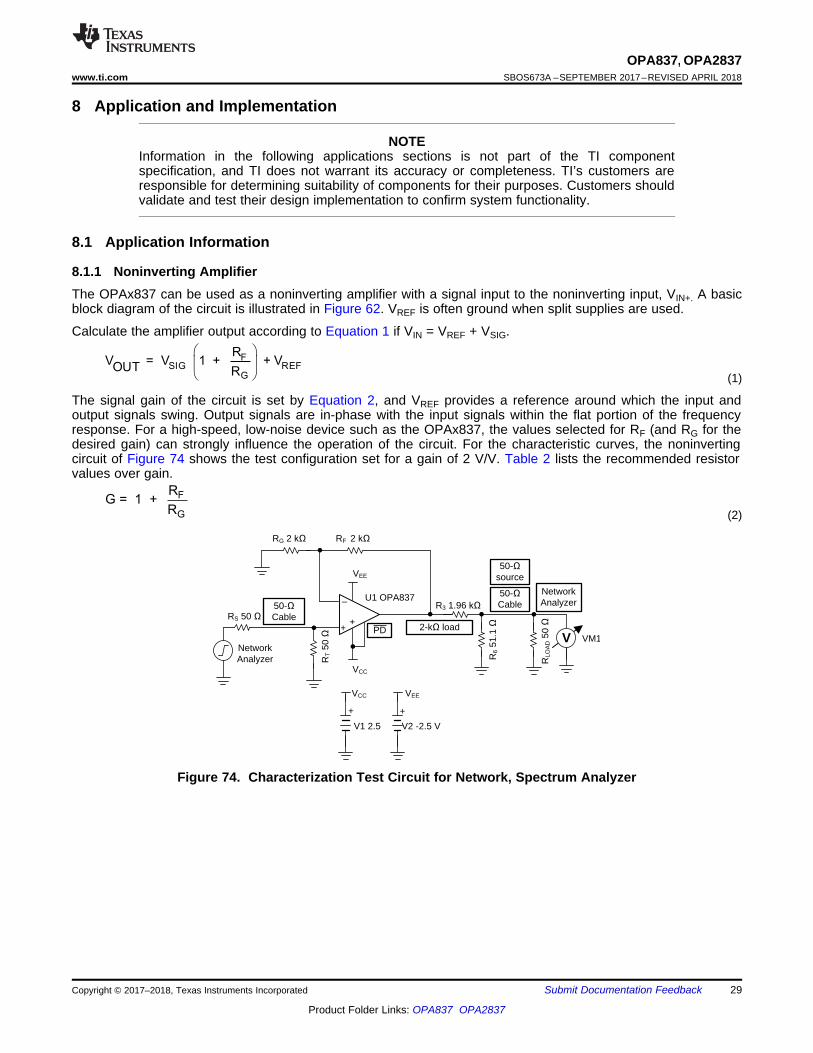
8.1.1 Noninverting AmplifierThe OPAx837 can be used as a noninverting amplifier with a signal input to the noninverting input, VIN+. A basicblock diagram of the circuit is illustrated in Figure 62. VREF is often ground when split supplies are used.
Calculate the amplifier output according to Equation 1 if VIN = VREF + VSIG.
(1)
The signal gain of the circuit is set by Equation 2, and VREF provides a reference around which the input andoutput signals swing. Output signals are in-phase with the input signals within the flat portion of the frequencyresponse. For a high-speed, low-noise device such as the OPAx837, the values selected for RF (and RG for thedesired gain) can strongly influence the operation of the circuit. For the characteristic curves, the noninvertingcircuit of Figure 74 shows the test configuration set for a gain of 2 V/V. Table 2 lists the recommended resistorvalues over gain.
(2)
Figure 74. Characterization Test Circuit for Network, Spectrum Analyzer

FSIG REF
G
RV = V + V
OUT R
æ ö-ç ÷è ø
30
OPA837, OPA2837SBOS673A –SEPTEMBER 2017–REVISED APRIL 2018 www.ti.com
Product Folder Links: OPA837 OPA2837
Submit Documentation Feedback Copyright © 2017–2018, Texas Instruments Incorporated
Application Information (continued)Table 2 lists the recommended resistor values from target gains of 1 V/V to 10 V/V where standard E96 valuesare shown. This table controls the RF and RG values to set the resistor noise contribution at approximately 50%of the total output noise power. These values increase the spot noise at the output over what the op amp voltagenoise produces by 41%. Lower values reduce the output noise of any design at the cost of more power in thefeedback circuit. Using the TINA model and simulation tool shows the impact of different resistor value choiceson response shape and noise.
Table 2. Noninverting Recommended Resistor ValuesTARGET GAIN (V/V) RF (Ω) RG (Ω) ACTUAL GAIN (V/V) GAIN (dB)
1 0 Open 1.00 0.001.5 1190 2370 1.50 3.532 2000 2000 2.00 6.023 2260 1130 3.00 9.544 2370 787 4.01 12.075 2490 619 5.02 14.026 2550 511 5.99 15.557 2610 432 7.04 16.958 2670 383 7.97 18.039 2670 332 9.04 19.1310 2670 294 10.08 20.07
8.1.2 Inverting AmplifierThe OPAx837 can be used as an inverting amplifier with a signal input to the inverting input, VIN–, through thegain-setting resistor RG. A basic block diagram of the circuit is illustrated in Figure 63.
The output of the amplifier can be calculated according to Equation 3 if VIN = VREF + VSIG and the noninvertinginput is biased to VREF.
(3)

RF 2 N�
+ PD+
±
RG 2 N��
VCC
VEE
VCC
+
Network Analyzer
+
VEE
RT 5
1.1 ��
+
2.5 V
RS 50 ���
-2.5 V
50-�Cable
Gain of -1 V/V
2-k� load Æ
50-�Cable
Š50-��source
Network Analyzer
R2
51.1
�
RLO
AD 5
0 �
V
R1 1.96 N�
- F
G
RG =
R
31
OPA837, OPA2837www.ti.com SBOS673A –SEPTEMBER 2017–REVISED APRIL 2018
Product Folder Links: OPA837 OPA2837
Submit Documentation FeedbackCopyright © 2017–2018, Texas Instruments Incorporated
The signal gain of the circuit is set by Equation 4 and VREF provides a reference point around which the input andoutput signals swing. For bipolar-supply operation, VREF is often ground. The output signal is 180˚ out-of-phasewith the input signal in the pass band of the application. Figure 75 shows the 50-Ω input matched configurationused for the inverting characterization plots set up for a gain of –1 V/V. In this case, an added terminationresistor, RT, is placed in parallel with the input RG resistor to provide an impedance match to 50-Ω testequipment. The output network appears as a 2-kΩ load but with a 50-Ω source to the network analyzer. Thisoutput interface network does add a 37.9-dB insertion loss that is normalized out in the characterization curves.Table 3 lists the suggested values for RF, RG, and RT for inverting gains from –0.5 V/V to –10 V/V. If a 50-Ω inputmatch is not required, eliminate the RT element.
(4)
Figure 75. Inverting Characterization Circuit for Network Analyzer
Table 3. Inverting Recommended Resistor ValuesINVERTING GAIN
(V/V) RF (Ω) RG (Ω) STANDARD RT(Ω) INPUT ZI (Ω) ACTUAL (V/V) GAIN (dB)
–0.5 1190 2370 51.1 50.02 –0.50 –5.98–1 2000 2000 51.1 49.83 –1.00 0.00–2 2260 1130 52.3 49.99 –2.00 6.02–3 2370 787 53.6 50.18 –3.01 9.58–4 2490 619 54.9 50.43 –4.02 12.09–5 2550 511 54.9 49.57 –4.99 13.96–6 2610 432 56.2 49.73 –6.04 15.62–7 2670 383 57.6 50.07 –6.97 16.87–8 2670 332 59 50.10 –8.04 18.11–9 2670 294 60.4 50.11 –9.08 19.16–10 2670 267 61.9 50.25 –10.00 20.00

� �2
22 BI F FN NI BN S S
I R 4kTRE E I R 4kTR
NG NG§ ·
� � � �¨ ¸© ¹
� � � �22 2O NI BN S S BI F FE E I R 4kTR NG I R 4kTR NGª º � � � �¬ ¼
OPA837 EO
RS
ENI
IBN
RG
RF
IBI
S4kTR
F4kTR
4kT = 1.6E ± 20J at 290° KG
4kTR
ERS
+
32
OPA837, OPA2837SBOS673A –SEPTEMBER 2017–REVISED APRIL 2018 www.ti.com
Product Folder Links: OPA837 OPA2837
Submit Documentation Feedback Copyright © 2017–2018, Texas Instruments Incorporated
8.1.3 Output DC Error CalculationsThe OPAx837 can provide excellent DC signal accuracy because of its high open-loop gain, high common-moderejection, high power-supply rejection, and low input offset voltage and bias current offset errors. To take fulladvantage of this low input offset voltage, pay careful attention to input bias current cancellation. The low-noiseinput stage for the OPAx837 has a relatively high input bias current (0.34 µA typical out the pins) but with a closematch between the two input currents. The OPAx837 is a negative rail input device using PNP input deviceswhere the base current flows out of the device pins. A large resistor to ground on the V+ input shifts the pinvoltage positively because of the input bias current. The mismatch between the two input bias currents is verylow, typically only ±10 nA of input offset current. Match the DC source impedances out of the two inputs toreduce the total output offset voltage. Figure 67 illustrates an example of resistor matching for bias currentcancellation. Analyzing the simple circuit of Figure 67 (using a gain of 2-V/V target with RF = RG = 2 kΩ)illustrates that the noise gain for the input offset voltage drift is 1 + 2 kΩ / 2 kΩ = 2 V/V. This value results in anoutput drift term of ±1.6 µV/°C × 2 = ±3.2 µV/°C (DCK package). Because the two impedances out of the inputsare matched, the residual error from the maximum ±250 pA/°C offset current drift is this maximum IOS drift timesthe 2-kΩ feedback resistor value, or ±50 µV/°C. The total output DC error drift band is ±53.2 µV/°C. If the outputDC drift is more important than reduced feedback currents, lower the resistor values to reduce the dominant driftterm resulting from the IOS term.
8.1.4 Output Noise CalculationsThe unity-gain stable, voltage-feedback OPAx837 op amp offers among the lowest input voltage and currentnoise terms for any device with a supply current less than 0.7 mA. Figure 76 shows the op amp noise analysismodel that includes all noise terms. In this model, all noise terms are shown as noise voltage or current densityterms in nV/√Hz or pA/√Hz.
Figure 76. Op Amp Noise Analysis Model
The total output spot noise voltage is computed as the square root of the squared contributing terms to theoutput noise voltage. This computation is adding all the contributing noise powers at the output by superposition,then taking the square root to return to a spot noise voltage. The last term includes the noise for both the RG andRF resistors. Equation 5 shows the general form for this output noise voltage using the terms presented inFigure 76.
(5)
Dividing this expression by the noise gain (NG = 1 + RF / RG), as shown in Equation 6, gives the equivalent inputreferred spot noise voltage at the noninverting input.
(6)
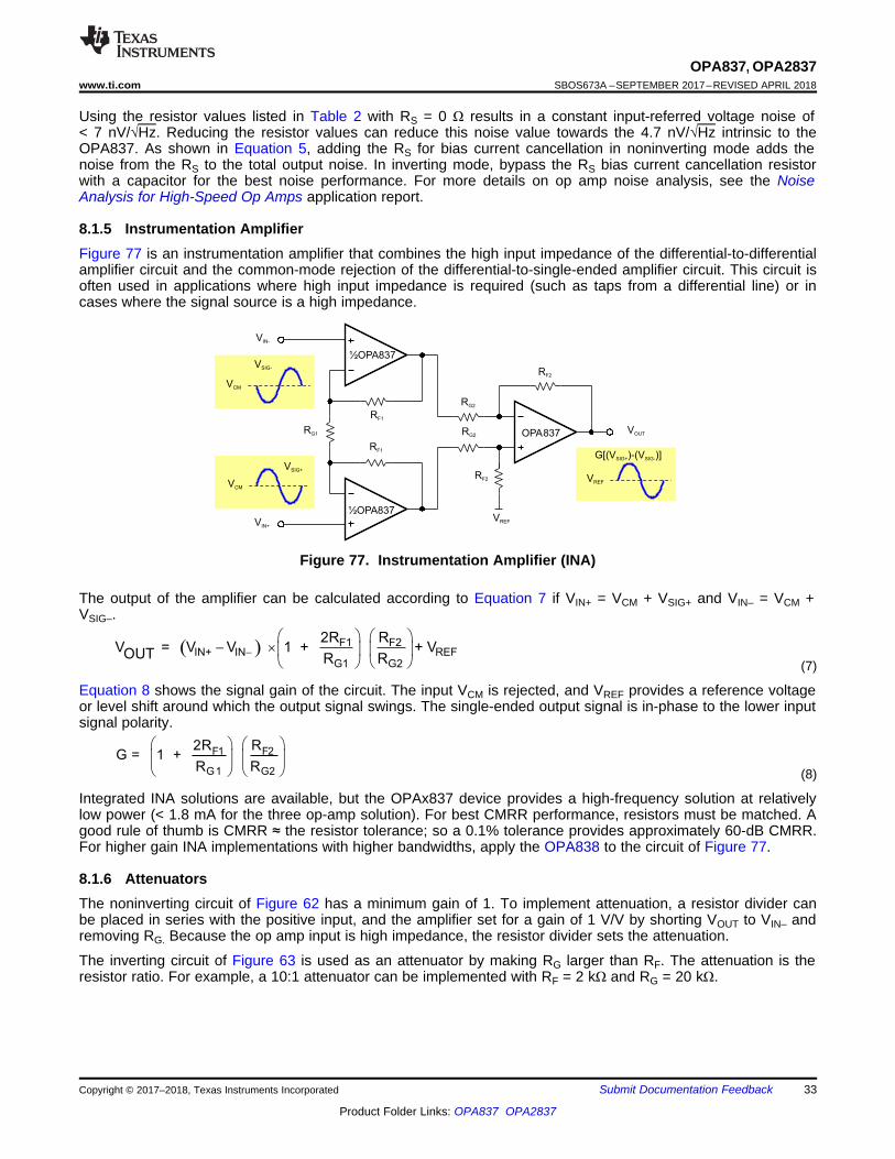
æ ö æ öç ÷ ç ÷è ø è ø
F1 F2
G1 G2
2R RG = 1 +
R R
( ) F1 F2IN+ IN REF
G1 G2
2R RV = V V 1 + + V
OUT R R-
æ ö æ ö- ´ç ÷ ç ÷
è ø è ø
OPA837
½OPA837
VIN-
VIN+
VSIG-
VSIG+
VCM
VCM
RG1
RF1
RF1
RG2
RG2
RF2
RF2
VOUT
G[(V )-(V )]SIG+ SIG-
VREF
VREF
½OPA837
33
OPA837, OPA2837www.ti.com SBOS673A –SEPTEMBER 2017–REVISED APRIL 2018
Product Folder Links: OPA837 OPA2837
Submit Documentation FeedbackCopyright © 2017–2018, Texas Instruments Incorporated
Using the resistor values listed in Table 2 with RS = 0 Ω results in a constant input-referred voltage noise of< 7 nV/√Hz. Reducing the resistor values can reduce this noise value towards the 4.7 nV/√Hz intrinsic to theOPA837. As shown in Equation 5, adding the RS for bias current cancellation in noninverting mode adds thenoise from the RS to the total output noise. In inverting mode, bypass the RS bias current cancellation resistorwith a capacitor for the best noise performance. For more details on op amp noise analysis, see the NoiseAnalysis for High-Speed Op Amps application report.
8.1.5 Instrumentation AmplifierFigure 77 is an instrumentation amplifier that combines the high input impedance of the differential-to-differentialamplifier circuit and the common-mode rejection of the differential-to-single-ended amplifier circuit. This circuit isoften used in applications where high input impedance is required (such as taps from a differential line) or incases where the signal source is a high impedance.
Figure 77. Instrumentation Amplifier (INA)
The output of the amplifier can be calculated according to Equation 7 if VIN+ = VCM + VSIG+ and VIN– = VCM +VSIG–.
(7)
Equation 8 shows the signal gain of the circuit. The input VCM is rejected, and VREF provides a reference voltageor level shift around which the output signal swings. The single-ended output signal is in-phase to the lower inputsignal polarity.
(8)
Integrated INA solutions are available, but the OPAx837 device provides a high-frequency solution at relativelylow power (< 1.8 mA for the three op-amp solution). For best CMRR performance, resistors must be matched. Agood rule of thumb is CMRR ≈ the resistor tolerance; so a 0.1% tolerance provides approximately 60-dB CMRR.For higher gain INA implementations with higher bandwidths, apply the OPA838 to the circuit of Figure 77.
8.1.6 AttenuatorsThe noninverting circuit of Figure 62 has a minimum gain of 1. To implement attenuation, a resistor divider canbe placed in series with the positive input, and the amplifier set for a gain of 1 V/V by shorting VOUT to VIN– andremoving RG. Because the op amp input is high impedance, the resistor divider sets the attenuation.
The inverting circuit of Figure 63 is used as an attenuator by making RG larger than RF. The attenuation is theresistor ratio. For example, a 10:1 attenuator can be implemented with RF = 2 kΩ and RG = 20 kΩ.

F
G
RG =
R
( )-
æ ö- ´ç ÷
è ø
FOUT IN+ IN REF
G
RV = V V + V
R
OPA837VIN+
VIN-
VCM
VCM
RG
RG
RF
RF
VREF
VSIG-
VSIG+
G[(V )-(V )]SIG+ SIG-
VOUT
VREF
34
OPA837, OPA2837SBOS673A –SEPTEMBER 2017–REVISED APRIL 2018 www.ti.com
Product Folder Links: OPA837 OPA2837
Submit Documentation Feedback Copyright © 2017–2018, Texas Instruments Incorporated
8.1.7 Differential to Single-Ended AmplifierFigure 78 shows a differential amplifier that converts differential signals to single-ended in a single stage andprovides gain (or attenuation) and level shifting. This circuit can be used in applications such as a line receiverfor converting a differential signal from a Cat5 cable to a single-ended output signal.
Figure 78. Differential to Single-Ended Amplifier
The output of the amplifier can be calculated according to Equation 9 if VIN+ = VCM + VSIG+ and VIN– = VCM +VSIG–.
(9)
The signal gain of the circuit is shown in Equation 10, VCM is rejected, and VREF provides a level shift orreference voltage around which the output signal swings. The single-ended output signal is in-phase with thenoninverting input signal. VREF is often ground when split supplies are used on the op amp.
(10)
Line termination can be accomplished by adding a shunt resistor across the VIN+ and VIN– inputs. The differentialimpedance is the shunt resistance in parallel with the input impedance of the amplifier circuit, which is usuallymuch higher. For low gain and low line impedance, the resistor value to add is approximately the impedance ofthe line. For example, if a 100-Ω Cat5 cable is used with a gain of 1 V/V amplifier and RF = RG = 2 kΩ, adding a100-Ω shunt across the input gives a differential impedance of 99 Ω, which is an adequate match for mostapplications.
For best CMRR performance, resistors must be matched. Assuming CMRR ≈ the resistor tolerance, a 0.1%tolerance provides approximately 60-dB CMRR.

F
G
2RG = 1 +
R
±
æ ö´ç ÷±
è ø
FIN CM
G
2RV = V 1 + + V
OUT R
GVSIG-
VIN-
VSIG-
VSIG+
VCM
VCM
RG
RF
RF
VIN+
VOUT-
VOUT+
VCM
VCM
GVSIG+
OPA837½
OPA837½
35
OPA837, OPA2837www.ti.com SBOS673A –SEPTEMBER 2017–REVISED APRIL 2018
Product Folder Links: OPA837 OPA2837
Submit Documentation FeedbackCopyright © 2017–2018, Texas Instruments Incorporated
8.1.8 Differential-to-Differential AmplifierFigure 79 shows a differential amplifier that is used to amplify differential signals to a differential output. Thiscircuit has high input impedance and is used in differential line driver applications where the signal source is ahigh-impedance driver (for example, a differential DAC) that must drive a line.
Figure 79. Differential-to-Differential Amplifier
The output of the amplifier can be calculated according to Equation 11 if VIN± is set to VCM + VSIG±.
(11)
The signal gain of the circuit is shown in Equation 12, and VCM passes with unity gain. The amplifier combinestwo noninverting amplifiers into one differential amplifier that shares the RG resistor, which makes RG effectivelyhalf its value when calculating the gain. The output signals are in-phase with the input signals.
(12)

OPA837
Signal and bias
from previous stage Signal and bias to
next stage
5 V
R1
RG
RF
GVSIG
0 V
0 V
VSIG
VOUT
RO
RF
OPA837
Signal and bias
from previous stage
Signal and bias to
next stage
5 V
R1
RG
0 V
VSIG
RO
VOUT
GVSIG
0 V
36
OPA837, OPA2837SBOS673A –SEPTEMBER 2017–REVISED APRIL 2018 www.ti.com
Product Folder Links: OPA837 OPA2837
Submit Documentation Feedback Copyright © 2017–2018, Texas Instruments Incorporated
8.1.9 Pulse Application With Single-Supply CircuitFor pulsed applications where the signal is at ground and pulses to a positive or negative voltage, the circuitbias-voltage considerations differ from those in an application with a signal that swings symmetrically around areference point. Figure 80 shows a circuit where the signal is at ground (0 V) and pulses to a positive value. Thewaveforms are shown slightly above ground because the output stage requires approximately 100 mV headroomto the supplies. To operate with the I/O swing truly to ground on a single-supply setup, consider using the fixed–0.23-V output LM7705.
Figure 80. Noninverting Single-Supply Circuit With Pulse
As shown in Figure 81, an inverting amplifier is more appropriate if the input signal pulses negative from ground.A key consideration in noninverting and inverting cases is that the input and output voltages are kept within thelimits of the amplifier. Because the VICR of the OPA837 includes the negative supply rail, the OPA837 op amp iswell-suited for this application.
Figure 81. Inverting Single-Supply Circuit With Pulse

4.096 V
ADS886016-Bit SAR
1 MSPS
REF5040
LM7705
OPA837
2.2 nF
3.3 VGND
GNDGND
GND
PD0 V 3.8 V
Gain = 1.05 V/V
0 V 4.0 V
+ 5.0 V
± 0.23 V+ 3.3 V
22 �
22 �
499 �
10.0 k�
+
±
+VCC
±VCC
37
OPA837, OPA2837www.ti.com SBOS673A –SEPTEMBER 2017–REVISED APRIL 2018
Product Folder Links: OPA837 OPA2837
Submit Documentation FeedbackCopyright © 2017–2018, Texas Instruments Incorporated
8.1.10 ADC Driver PerformanceThe OPAx837 provides excellent performance when driving high-performance delta-sigma (ΔΣ) or successive-approximation-register (SAR) ADCs in low-power audio and industrial applications.
Figure 82 repeats the front page diagram. Many designs prefer to work with a true 0-V input range to 0-V outputat the ADC. The 100-mV output headroom requirement for the OPAx837 then requires a small negative supply tohold the output linearity to ground. This supply is provided in this example using the low-cost LM7705 fixednegative, –0.23-V output regulator. On a 5-V supply, the input headroom requires at least a 1.2-V headroom tothat supply. As shown in Figure 82, this requirement limits the maximum input to 3.8 V. The SAR operates with aprecision 4.096-V reference provided by the REF5040, where the gain of 1.05 V/V takes the 3.8-V maximuminput to a 4.0-V maximum output. The RC values have been set to limit the overshoot at the OPAx837 output pinto reduce clipping on fast (50 ns) transitions.
Figure 82. OPA837 and ADS8860 Example Circuit

OPA8375.6 nF
147 W 255 W
12 nF
OPA837
430 pF
1.4 kW
1.4 kW 1.91 kW
2.2 nF
38
OPA837, OPA2837SBOS673A –SEPTEMBER 2017–REVISED APRIL 2018 www.ti.com
Product Folder Links: OPA837 OPA2837
Submit Documentation Feedback Copyright © 2017–2018, Texas Instruments Incorporated
8.2 Typical Applications
8.2.1 Active FiltersThe OPAx837 is a good choice for active filters. Figure 83 and Figure 84 show MFB and Sallen-Key circuitsdesigned implementing second-order, low-pass Butterworth filter circuits. Figure 85 illustrates the frequencyresponse.
The main difference is that the MFB active filter provides an inverting amplifier in the pass band and the Sallen-Key active filter is noninverting. The primary advantage for each active filter is that the Sallen-Key filter in unitygain has no resistor gain error term or feedback resistor noise contribution. The MFB active filter has betterattenuation properties beyond the bandwidth of the op amp. The example circuits are assuming a split-supplyoperation but single-supply operation is possible with midscale biasing.
Figure 83. MFB Active Filter, 100-kHz, Second-Order, Low-Pass Butterworth Filter Circuit
Figure 84. Sallen-Key Active Filter, 100-kHz, Second-Order, Low-Pass Butterworth Filter Circuit
8.2.1.1 Design RequirementsFor both designs, target the following filter shape characteristic:• Gain of 1 V/V• 100-kHz Butterworth response• Q = 0.707 gives a flat Butterworth design
Scale the resistors down to reduce their noise contribution. In the MFB design, the input resistor is the in-bandload to the prior stage. Use values slightly below the gain of –1 V/V in Table 3. The Sallen-Key filter shows ahigh impedance input in-band, so scale those resistors down further to improve noise.
The output DC error and drift can be improved by adding bias current cancellation resistors. For the MFB filterthat is a resistor (and a noise filter capacitor) on the noninverting input to ground equal to the resistor inside theloop times the noise gain. For the Sallen-Key design, add a feedback resistor equal to the sum of the two inputresistors.
8.2.1.2 Detailed Design ProcedureThe filter designs shown in this section used an improved design flow that reduces the resistor noise and noisegain peaking. For the MFB filter, the design was based on the information in the Design Methodology for MFBFilters in ADC Interface Applications application note.
For the Sallen-Key design, the solution is based on the information in the Component Pre-Distortion for SallenKey Filters application note.
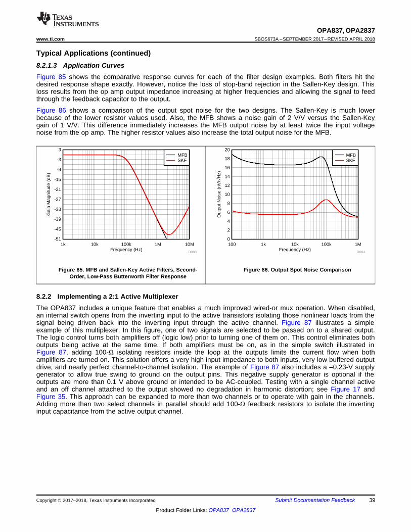
Frequency (Hz)
Gai
n M
agni
tude
(dB
)
-51
-45
-39
-33
-27
-21
-15
-9
-3
3
1k 10k 100k 1M 10M
D083
MFBSKF
Frequency (Hz)
Out
put N
oise
(nV
/�H
z)
0
2
4
6
8
10
12
14
16
18
20
100 1k 10k 100k 1M
D084
MFBSKF
39
OPA837, OPA2837www.ti.com SBOS673A –SEPTEMBER 2017–REVISED APRIL 2018
Product Folder Links: OPA837 OPA2837
Submit Documentation FeedbackCopyright © 2017–2018, Texas Instruments Incorporated
Typical Applications (continued)8.2.1.3 Application CurvesFigure 85 shows the comparative response curves for each of the filter design examples. Both filters hit thedesired response shape exactly. However, notice the loss of stop-band rejection in the Sallen-Key design. Thisloss results from the op amp output impedance increasing at higher frequencies and allowing the signal to feedthrough the feedback capacitor to the output.
Figure 86 shows a comparison of the output spot noise for the two designs. The Sallen-Key is much lowerbecause of the lower resistor values used. Also, the MFB shows a noise gain of 2 V/V versus the Sallen-Keygain of 1 V/V. This difference immediately increases the MFB output noise by at least twice the input voltagenoise from the op amp. The higher resistor values also increase the total output noise for the MFB.
Figure 85. MFB and Sallen-Key Active Filters, Second-Order, Low-Pass Butterworth Filter Response
Figure 86. Output Spot Noise Comparison
8.2.2 Implementing a 2:1 Active MultiplexerThe OPA837 includes a unique feature that enables a much improved wired-or mux operation. When disabled,an internal switch opens from the inverting input to the active transistors isolating those nonlinear loads from thesignal being driven back into the inverting input through the active channel. Figure 87 illustrates a simpleexample of this multiplexer. In this figure, one of two signals are selected to be passed on to a shared output.The logic control turns both amplifiers off (logic low) prior to turning one of them on. This control eliminates bothoutputs being active at the same time. If both amplifiers must be on, as in the simple switch illustrated inFigure 87, adding 100-Ω isolating resistors inside the loop at the outputs limits the current flow when bothamplifiers are turned on. This solution offers a very high input impedance to both inputs, very low buffered outputdrive, and nearly perfect channel-to-channel isolation. The example of Figure 87 also includes a –0.23-V supplygenerator to allow true swing to ground on the output pins. This negative supply generator is optional if theoutputs are more than 0.1 V above ground or intended to be AC-coupled. Testing with a single channel activeand an off channel attached to the output showed no degradation in harmonic distortion; see Figure 17 andFigure 35. This approach can be expanded to more than two channels or to operate with gain in the channels.Adding more than two select channels in parallel should add 100-Ω feedback resistors to isolate the invertinginput capacitance from the active output channel.

+
VIN 1
++
+
Å9
S
VIN 2
Å9S+VS
+V
S
VOUT
R3
2 k
R7 100 k +VS
R6 100 k +VS
U1 OPA837
U2 OPA837
LM7705 ± 230 mV
2X1 Active Mux
PD
This line isactuallya logic
line
VS1 5
+
+
Å
Å9
S+
VS
PD
+
+
Å
40
OPA837, OPA2837SBOS673A –SEPTEMBER 2017–REVISED APRIL 2018 www.ti.com
Product Folder Links: OPA837 OPA2837
Submit Documentation Feedback Copyright © 2017–2018, Texas Instruments Incorporated
Typical Applications (continued)
Figure 87. 2:1 Active Multiplexer
8.2.2.1 Design RequirementsTo implement a 2:1 active mux, connect the outputs of two OPA837 devices together with separate input signals.If termination is required for the input signals, add this termination as a resistor to ground on the noninvertinginputs. The inputs accept an input range from 0 V to 3.8 V by using a negative 0.23-V supply generator, such asthe LM7705.
8.2.2.2 Detailed Design ProcedureAside from simply connecting the two outputs together as shown in Figure 87, there are several otherconsiderations as well:• If the source impedance is not 0 Ω, consider adding a resistor in the feedback networks equal to that source
impedance to reduce the output DC error resulting from bias currents• If the logic control can place both channels on at the same time, place 100-Ω resistors inside the feedback
loop to limit supply currents when both outputs are active• If a matched gain is desired for the two inputs, configure the op amps for that gain instead of gain of 1 V/V• If the load is capacitive, add the required ROUT before the summing point on each op amp output

OPA837
++
This line isactuallya logic
line
VIN
Å9S
+VS
R5 2 k
PD
Å9S
+VS
R4 2 k
R1 100 k +VS
PD
R2 100 k
+VS
R3
1 k
+VS Å9S
OPA837
Gain of 2 orGain of 1
1-Bit PGA
VS1 2.5 VS1 Å2.5
++
++
VOUT
Å9S
41
OPA837, OPA2837www.ti.com SBOS673A –SEPTEMBER 2017–REVISED APRIL 2018
Product Folder Links: OPA837 OPA2837
Submit Documentation FeedbackCopyright © 2017–2018, Texas Instruments Incorporated
Typical Applications (continued)8.2.3 1-Bit PGA OperationUsing the internal inverting input switch that operates along with the power disable function can also allow asimple gain selection on a single input signal. Figure 88 shows an example gain select of either 1 V/V or 2 V/Vfrom a single input to a single output. The logic disables both channels before turning one of them on to avoidhigh currents in both outputs to be active at the same time. If this approach is not possible, as in the simpleswitch shown in Figure 88, insert 100-Ω resistors inside the loop of each op amp output. A bipolar supply isshown in Figure 88, but any of the single-supply options are also possible. Any combination of gains can beimplemented, but wide gain ranges show a larger change in signal bandwidth. This approach can be expandedto more than two gain settings. Testing with the circuit of Figure 88 showed no change in harmonic distortion;see Figure 18 and Figure 36.
Figure 88. 1-Bit PGA
8.2.3.1 Design RequirementsConfigure two OPA837 device outputs in different gains when driving the noninverting input with the same inputsignal. Select one the two channels using the disable control. Set one channel to a gain of 1 V/V and the secondchannel to a gain of 2 V/V using the recommended 2-kΩ values from Table 2.
8.2.3.2 Detailed Design ProcedureThe simple design of Figure 88 has several options and details to consider, which include:• For split-supply operation, the disable control line must operate to within 0.55 V of the negative supply to
disable a channel. A logic level shift is required.• Any combination of gains can be implemented. However, the signal bandwidths may vary widely through the
gain bandwidth product effect between the two channels if the gains are widely separated. If a more constantbandwidth between gains is desired, consider adding a fixed RC filter after the combined outputs at a lowercutoff frequency than the slowest gain setting.

42
OPA837, OPA2837SBOS673A –SEPTEMBER 2017–REVISED APRIL 2018 www.ti.com
Product Folder Links: OPA837 OPA2837
Submit Documentation Feedback Copyright © 2017–2018, Texas Instruments Incorporated
9 Power Supply RecommendationsThe OPAx837 is intended to work in a nominal supply range of 3.0 V to 5 V. Supply-voltage tolerances aresupported with the specified operating range of 2.7 V (–10% on a 3-V supply) and 5.4 V (+8% on a 5-V supply).Good power-supply bypassing is required. Minimize the distance (< 0.1 inch) from the power-supply pins to high-frequency, 0.1-µF decoupling capacitors. A larger capacitor (2.2 µF is typical) is used along with a high-frequency, 0.1-µF supply-decoupling capacitor at the device supply pins. For single-supply operation, only thepositive supply has these capacitors. When a split supply is used, use these capacitors for each supply toground. If necessary, place the larger capacitors further from the device and share these capacitors amongseveral devices in the same area of the printed circuit board (PCB). Avoid narrow power and ground traces tominimize inductance between the pins and the decoupling capacitors. An optional supply decoupling capacitoracross the two power supplies (for bipolar operation) reduces second harmonic distortion.
The OPA837 has a positive supply current temperature coefficient; see Figure 57. This coefficient helps improvethe input offset voltage drift. Supply current requirements in the system design must account for this effect usingthe maximum intended ambient and Figure 57 to size the supply required. The very low power dissipation for theOPA837 typically does not require any special thermal design considerations. For the extreme case of 125°Coperating ambient, use the approximate maximum 200°C/W for the two packages, and a maximum internalpower of 5.4-V supply × 0.8-mA 125°C supply current from Figure 57 gives a maximum internal power of4.3 mW. This power only gives a 0.86°C rise from ambient to junction temperature, which is well below themaximum 150°C junction temperature. Load power adds to this value, but also increases the junctiontemperature only slightly over ambient temperature.
10 Layout
10.1 Layout GuidelinesThe OPA837EVM can be used as a reference when designing the circuit board. TI recommends following theEVM layout of the external components near to the amplifier, ground plane construction, and power routing asclosely as possible. General guidelines are listed below:1. Signal routing must be direct and as short as possible into and out of the op amp.2. The feedback path must be short and direct avoiding vias if possible, especially with G = 1 V/V.3. Ground or power planes must be removed from directly under the negative input and output pins of the
amplifier.4. TI recommends placing a series output resistor as close to the output pin as possible. See Figure 49 for
recommended values for the expected capacitive load. These values are derived targeting a 30° phasemargin to the output of the op amp.
5. A 2.2-µF power-supply decoupling capacitor must be placed within two inches of the device and can beshared with other op amps. For split supply, a capacitor is required for both supplies.
6. A 0.1-µF power-supply decoupling capacitor must be placed as close to the supply pins as possible,preferably within 0.1 inch. For split supply, a capacitor is required for both supplies.
7. The PD pin uses low logic swing levels. If the pin is not used, PD must be tied to the positive supply toenable the amplifier. If the pin is used, PD must be actively driven. A bypass capacitor is not necessary, butcan be used for robustness in noisy environments.

Place bypass capacitors close to power pins
Place input resistor close to pin 4to minimize stray capacitance
Place output resistors close to output pins to minimize
parasitic capacitance
Ground and power plane removed from inner layers
Ground and power plane exist on inner layers
1
2
6
4
5
+ ±
Place bypass capacitors close to power pins
Remove GND and Power plane under pins 1 and 4 to minimize
stray PCB capacitance
Place feedback resistor on the bottom of PCB between pins 4 and 6
Power control (disable) pinMust be driven
Non-inverting input terminated in 50 ��
3
43
OPA837, OPA2837www.ti.com SBOS673A –SEPTEMBER 2017–REVISED APRIL 2018
Product Folder Links: OPA837 OPA2837
Submit Documentation FeedbackCopyright © 2017–2018, Texas Instruments Incorporated
10.2 Layout Example
Figure 89. EVM Layout Example

44
OPA837, OPA2837SBOS673A –SEPTEMBER 2017–REVISED APRIL 2018 www.ti.com
Product Folder Links: OPA837 OPA2837
Submit Documentation Feedback Copyright © 2017–2018, Texas Instruments Incorporated
11 Device and Documentation Support
11.1 Documentation Support
11.1.1 Related DocumentationFor related documentation see the following:• ADS8860 16-Bit, 1-MSPS, Serial Interface, microPower, Miniature, Single-Ended Input, SAR Analog-to-Digital
Converter• LM7705 Low-Noise Negative Bias Generator• OPA838 1-mA, 300-MHz Gain Bandwidth, Voltage-Feedback Op Amp• REF50xx Low-Noise, Very Low Drift, Precision Voltage Reference• OPA837DBV, OPA836DBV EVM• Single-Supply Op Amp Design Techniques• Noise Analysis for High-Speed Op Amps• Design Methodology for MFB Filters in ADC Interface Applications• Component Pre-Distortion for Sallen Key Filters• TINA model and simulation tool
11.2 Related LinksThe table below lists quick access links. Categories include technical documents, support and communityresources, tools and software, and quick access to order now.
Table 4. Related Links
PARTS PRODUCT FOLDER ORDER NOW TECHNICALDOCUMENTS
TOOLS &SOFTWARE
SUPPORT &COMMUNITY
OPA837 Click here Click here Click here Click here Click hereOPA2837 Click here Click here Click here Click here Click here
11.3 Receiving Notification of Documentation UpdatesTo receive notification of documentation updates, navigate to the device product folder on ti.com. In the upperright corner, click on Alert me to register and receive a weekly digest of any product information that haschanged. For change details, review the revision history included in any revised document.
11.4 Community ResourcesThe following links connect to TI community resources. Linked contents are provided "AS IS" by the respectivecontributors. They do not constitute TI specifications and do not necessarily reflect TI's views; see TI's Terms ofUse.
TI E2E™ Online Community TI's Engineer-to-Engineer (E2E) Community. Created to foster collaborationamong engineers. At e2e.ti.com, you can ask questions, share knowledge, explore ideas and helpsolve problems with fellow engineers.
Design Support TI's Design Support Quickly find helpful E2E forums along with design support tools andcontact information for technical support.
11.5 TrademarksE2E is a trademark of Texas Instruments.All other trademarks are the property of their respective owners.
11.6 Electrostatic Discharge CautionThese devices have limited built-in ESD protection. The leads should be shorted together or the device placed in conductive foamduring storage or handling to prevent electrostatic damage to the MOS gates.

45
OPA837, OPA2837www.ti.com SBOS673A –SEPTEMBER 2017–REVISED APRIL 2018
Product Folder Links: OPA837 OPA2837
Submit Documentation FeedbackCopyright © 2017–2018, Texas Instruments Incorporated
11.7 GlossarySLYZ022 — TI Glossary.
This glossary lists and explains terms, acronyms, and definitions.
12 Mechanical, Packaging, and Orderable InformationThe following pages include mechanical, packaging, and orderable information. This information is the mostcurrent data available for the designated devices. This data is subject to change without notice and revision ofthis document. For browser-based versions of this data sheet, refer to the left-hand navigation.

PACKAGE OPTION ADDENDUM
www.ti.com 24-Apr-2018
Addendum-Page 1
PACKAGING INFORMATION
Orderable Device Status(1)
Package Type PackageDrawing
Pins PackageQty
Eco Plan(2)
Lead/Ball Finish(6)
MSL Peak Temp(3)
Op Temp (°C) Device Marking(4/5)
Samples
OPA2837IDGKR ACTIVE VSSOP DGK 8 2500 Green (RoHS& no Sb/Br)
CU NIPDAUAG Level-2-260C-1 YEAR -40 to 125 2837
OPA2837IDGKT ACTIVE VSSOP DGK 8 250 Green (RoHS& no Sb/Br)
CU NIPDAUAG Level-2-260C-1 YEAR -40 to 125 2837
OPA2837IRUNR PREVIEW QFN RUN 10 2500 TBD Call TI Call TI -40 to 125
OPA2837IRUNT PREVIEW QFN RUN 10 250 TBD Call TI Call TI -40 to 125
OPA837IDBVR ACTIVE SOT-23 DBV 6 3000 Green (RoHS& no Sb/Br)
CU NIPDAU Level-2-260C-1 YEAR -40 to 125 19FF
OPA837IDBVT ACTIVE SOT-23 DBV 6 250 Green (RoHS& no Sb/Br)
CU NIPDAU Level-2-260C-1 YEAR -40 to 125 19FF
OPA837IDCKR ACTIVE SC70 DCK 5 3000 Green (RoHS& no Sb/Br)
CU NIPDAU Level-2-260C-1 YEAR -40 to 125 16K
OPA837IDCKT ACTIVE SC70 DCK 5 250 Green (RoHS& no Sb/Br)
CU NIPDAU Level-2-260C-1 YEAR -40 to 125 16K
(1) The marketing status values are defined as follows:ACTIVE: Product device recommended for new designs.LIFEBUY: TI has announced that the device will be discontinued, and a lifetime-buy period is in effect.NRND: Not recommended for new designs. Device is in production to support existing customers, but TI does not recommend using this part in a new design.PREVIEW: Device has been announced but is not in production. Samples may or may not be available.OBSOLETE: TI has discontinued the production of the device.
(2) RoHS: TI defines "RoHS" to mean semiconductor products that are compliant with the current EU RoHS requirements for all 10 RoHS substances, including the requirement that RoHS substancedo not exceed 0.1% by weight in homogeneous materials. Where designed to be soldered at high temperatures, "RoHS" products are suitable for use in specified lead-free processes. TI mayreference these types of products as "Pb-Free".RoHS Exempt: TI defines "RoHS Exempt" to mean products that contain lead but are compliant with EU RoHS pursuant to a specific EU RoHS exemption.Green: TI defines "Green" to mean the content of Chlorine (Cl) and Bromine (Br) based flame retardants meet JS709B low halogen requirements of <=1000ppm threshold. Antimony trioxide basedflame retardants must also meet the <=1000ppm threshold requirement.
(3) MSL, Peak Temp. - The Moisture Sensitivity Level rating according to the JEDEC industry standard classifications, and peak solder temperature.
(4) There may be additional marking, which relates to the logo, the lot trace code information, or the environmental category on the device.
(5) Multiple Device Markings will be inside parentheses. Only one Device Marking contained in parentheses and separated by a "~" will appear on a device. If a line is indented then it is a continuationof the previous line and the two combined represent the entire Device Marking for that device.

PACKAGE OPTION ADDENDUM
www.ti.com 24-Apr-2018
Addendum-Page 2
(6) Lead/Ball Finish - Orderable Devices may have multiple material finish options. Finish options are separated by a vertical ruled line. Lead/Ball Finish values may wrap to two lines if the finishvalue exceeds the maximum column width.
Important Information and Disclaimer:The information provided on this page represents TI's knowledge and belief as of the date that it is provided. TI bases its knowledge and belief on informationprovided by third parties, and makes no representation or warranty as to the accuracy of such information. Efforts are underway to better integrate information from third parties. TI has taken andcontinues to take reasonable steps to provide representative and accurate information but may not have conducted destructive testing or chemical analysis on incoming materials and chemicals.TI and TI suppliers consider certain information to be proprietary, and thus CAS numbers and other limited information may not be available for release.
In no event shall TI's liability arising out of such information exceed the total purchase price of the TI part(s) at issue in this document sold by TI to Customer on an annual basis.

TAPE AND REEL INFORMATION
*All dimensions are nominal
Device PackageType
PackageDrawing
Pins SPQ ReelDiameter
(mm)
ReelWidth
W1 (mm)
A0(mm)
B0(mm)
K0(mm)
P1(mm)
W(mm)
Pin1Quadrant
OPA2837IDGKR VSSOP DGK 8 2500 330.0 12.4 5.3 3.4 1.4 8.0 12.0 Q1
OPA2837IDGKT VSSOP DGK 8 250 330.0 12.4 5.3 3.4 1.4 8.0 12.0 Q1
OPA837IDBVR SOT-23 DBV 6 3000 178.0 9.0 3.23 3.17 1.37 4.0 8.0 Q3
OPA837IDBVT SOT-23 DBV 6 250 178.0 9.0 3.23 3.17 1.37 4.0 8.0 Q3
OPA837IDCKR SC70 DCK 5 3000 178.0 9.0 2.4 2.5 1.2 4.0 8.0 Q3
OPA837IDCKT SC70 DCK 5 250 178.0 9.0 2.4 2.5 1.2 4.0 8.0 Q3
PACKAGE MATERIALS INFORMATION
www.ti.com 30-Apr-2018
Pack Materials-Page 1

*All dimensions are nominal
Device Package Type Package Drawing Pins SPQ Length (mm) Width (mm) Height (mm)
OPA2837IDGKR VSSOP DGK 8 2500 366.0 364.0 50.0
OPA2837IDGKT VSSOP DGK 8 250 366.0 364.0 50.0
OPA837IDBVR SOT-23 DBV 6 3000 180.0 180.0 18.0
OPA837IDBVT SOT-23 DBV 6 250 180.0 180.0 18.0
OPA837IDCKR SC70 DCK 5 3000 180.0 180.0 18.0
OPA837IDCKT SC70 DCK 5 250 180.0 180.0 18.0
PACKAGE MATERIALS INFORMATION
www.ti.com 30-Apr-2018
Pack Materials-Page 2


IMPORTANT NOTICE
Texas Instruments Incorporated (TI) reserves the right to make corrections, enhancements, improvements and other changes to itssemiconductor products and services per JESD46, latest issue, and to discontinue any product or service per JESD48, latest issue. Buyersshould obtain the latest relevant information before placing orders and should verify that such information is current and complete.TI’s published terms of sale for semiconductor products (http://www.ti.com/sc/docs/stdterms.htm) apply to the sale of packaged integratedcircuit products that TI has qualified and released to market. Additional terms may apply to the use or sale of other types of TI products andservices.Reproduction of significant portions of TI information in TI data sheets is permissible only if reproduction is without alteration and isaccompanied by all associated warranties, conditions, limitations, and notices. TI is not responsible or liable for such reproduceddocumentation. Information of third parties may be subject to additional restrictions. Resale of TI products or services with statementsdifferent from or beyond the parameters stated by TI for that product or service voids all express and any implied warranties for theassociated TI product or service and is an unfair and deceptive business practice. TI is not responsible or liable for any such statements.Buyers and others who are developing systems that incorporate TI products (collectively, “Designers”) understand and agree that Designersremain responsible for using their independent analysis, evaluation and judgment in designing their applications and that Designers havefull and exclusive responsibility to assure the safety of Designers' applications and compliance of their applications (and of all TI productsused in or for Designers’ applications) with all applicable regulations, laws and other applicable requirements. Designer represents that, withrespect to their applications, Designer has all the necessary expertise to create and implement safeguards that (1) anticipate dangerousconsequences of failures, (2) monitor failures and their consequences, and (3) lessen the likelihood of failures that might cause harm andtake appropriate actions. Designer agrees that prior to using or distributing any applications that include TI products, Designer willthoroughly test such applications and the functionality of such TI products as used in such applications.TI’s provision of technical, application or other design advice, quality characterization, reliability data or other services or information,including, but not limited to, reference designs and materials relating to evaluation modules, (collectively, “TI Resources”) are intended toassist designers who are developing applications that incorporate TI products; by downloading, accessing or using TI Resources in anyway, Designer (individually or, if Designer is acting on behalf of a company, Designer’s company) agrees to use any particular TI Resourcesolely for this purpose and subject to the terms of this Notice.TI’s provision of TI Resources does not expand or otherwise alter TI’s applicable published warranties or warranty disclaimers for TIproducts, and no additional obligations or liabilities arise from TI providing such TI Resources. TI reserves the right to make corrections,enhancements, improvements and other changes to its TI Resources. TI has not conducted any testing other than that specificallydescribed in the published documentation for a particular TI Resource.Designer is authorized to use, copy and modify any individual TI Resource only in connection with the development of applications thatinclude the TI product(s) identified in such TI Resource. NO OTHER LICENSE, EXPRESS OR IMPLIED, BY ESTOPPEL OR OTHERWISETO ANY OTHER TI INTELLECTUAL PROPERTY RIGHT, AND NO LICENSE TO ANY TECHNOLOGY OR INTELLECTUAL PROPERTYRIGHT OF TI OR ANY THIRD PARTY IS GRANTED HEREIN, including but not limited to any patent right, copyright, mask work right, orother intellectual property right relating to any combination, machine, or process in which TI products or services are used. Informationregarding or referencing third-party products or services does not constitute a license to use such products or services, or a warranty orendorsement thereof. Use of TI Resources may require a license from a third party under the patents or other intellectual property of thethird party, or a license from TI under the patents or other intellectual property of TI.TI RESOURCES ARE PROVIDED “AS IS” AND WITH ALL FAULTS. TI DISCLAIMS ALL OTHER WARRANTIES ORREPRESENTATIONS, EXPRESS OR IMPLIED, REGARDING RESOURCES OR USE THEREOF, INCLUDING BUT NOT LIMITED TOACCURACY OR COMPLETENESS, TITLE, ANY EPIDEMIC FAILURE WARRANTY AND ANY IMPLIED WARRANTIES OFMERCHANTABILITY, FITNESS FOR A PARTICULAR PURPOSE, AND NON-INFRINGEMENT OF ANY THIRD PARTY INTELLECTUALPROPERTY RIGHTS. TI SHALL NOT BE LIABLE FOR AND SHALL NOT DEFEND OR INDEMNIFY DESIGNER AGAINST ANY CLAIM,INCLUDING BUT NOT LIMITED TO ANY INFRINGEMENT CLAIM THAT RELATES TO OR IS BASED ON ANY COMBINATION OFPRODUCTS EVEN IF DESCRIBED IN TI RESOURCES OR OTHERWISE. IN NO EVENT SHALL TI BE LIABLE FOR ANY ACTUAL,DIRECT, SPECIAL, COLLATERAL, INDIRECT, PUNITIVE, INCIDENTAL, CONSEQUENTIAL OR EXEMPLARY DAMAGES INCONNECTION WITH OR ARISING OUT OF TI RESOURCES OR USE THEREOF, AND REGARDLESS OF WHETHER TI HAS BEENADVISED OF THE POSSIBILITY OF SUCH DAMAGES.Unless TI has explicitly designated an individual product as meeting the requirements of a particular industry standard (e.g., ISO/TS 16949and ISO 26262), TI is not responsible for any failure to meet such industry standard requirements.Where TI specifically promotes products as facilitating functional safety or as compliant with industry functional safety standards, suchproducts are intended to help enable customers to design and create their own applications that meet applicable functional safety standardsand requirements. Using products in an application does not by itself establish any safety features in the application. Designers mustensure compliance with safety-related requirements and standards applicable to their applications. Designer may not use any TI products inlife-critical medical equipment unless authorized officers of the parties have executed a special contract specifically governing such use.Life-critical medical equipment is medical equipment where failure of such equipment would cause serious bodily injury or death (e.g., lifesupport, pacemakers, defibrillators, heart pumps, neurostimulators, and implantables). Such equipment includes, without limitation, allmedical devices identified by the U.S. Food and Drug Administration as Class III devices and equivalent classifications outside the U.S.TI may expressly designate certain products as completing a particular qualification (e.g., Q100, Military Grade, or Enhanced Product).Designers agree that it has the necessary expertise to select the product with the appropriate qualification designation for their applicationsand that proper product selection is at Designers’ own risk. Designers are solely responsible for compliance with all legal and regulatoryrequirements in connection with such selection.Designer will fully indemnify TI and its representatives against any damages, costs, losses, and/or liabilities arising out of Designer’s non-compliance with the terms and provisions of this Notice.
Mailing Address: Texas Instruments, Post Office Box 655303, Dallas, Texas 75265Copyright © 2018, Texas Instruments Incorporated