Embed Size (px)
Citation preview

OPA244OPA2244OPA4244
®
© 1999 Burr-Brown Corporation PDS-1437C Printed in U.S.A. December, 1999
FEATURES Micro SIZE PACKAGES
OPA244 (Single): SOT-23-5OPA2244 (Dual): MSOP-8OPA4244 (Quad): TSSOP-14
Micro POWER: IQ = 50µA/channel SINGLE SUPPLY OPERATION WIDE BANDWIDTH: 430kHz WIDE SUPPLY RANGE:
Single Supply: 2.2V to 36VDual Supply: ±1.1V to ±18V
DESCRIPTIONThe OPA244 (single), OPA2244 (dual), and OPA4244 (quad)op amps are designed for very low quiescent current(50µA/channel), yet achieve excellent bandwidth. Ideal forbattery powered and portable instrumentation, all versions areoffered in micro packages for space-limited applications.The dual and quad versions feature completely independentcircuitry for lowest crosstalk and freedom from interaction, evenwhen overdriven or overloaded.The OPA244 series is easy to use and free from phaseinversion and overload problems found in some other op amps.These amplifiers are stable in unity gain and excellent perfor-mance is maintained as they swing to their specified limits.They can be operated from single (+2.2V to +36V) or dualsupplies (±1.1V to ±18V). The input common-mode voltagerange includes ground—ideal for many single supply applica-tions. All versions have similar performance. However, thereare some differences, such as common-mode rejection. Allversions are interchangeable in most applications.All versions are offered in miniature, surface-mount packages.OPA244 (single version) comes in the tiny 5-lead SOT-23-5surface mount, SO-8 surface mount, and 8-pin DIP. OPA2244(dual version) is available in the MSOP-8 surface mount,SO-8 surface-mount, and 8-pin DIP. The OPA4244 (quad)comes in the TSSOP-14 surface mount. They are fully specifiedfrom –40°C to +85°C and operate from –55°C to +125°C.A SPICE Macromodel is available for design analysis.
Micro Power, Single-SupplyOPERATIONAL AMPLIFIERS
Micro Amplifier ™ Series
APPLICATIONS BATTERY POWERED SYSTEMS PORTABLE EQUIPMENT PCMCIA CARDS BATTERY PACKS AND POWER SUPPLIES CONSUMER PRODUCTS
1
2
3
4
8
7
6
5
V+
Out B
–In B
+In B
Out A
–In A
+In A
V–
OPA2244
8-Pin DIP, SO-8, MSOP-8
A
B
1
2
3
5
4
V+
–In
Out
V–
+In
OPA244
SOT-23-5
1
2
3
4
8
7
6
5
NC
V+
Output
NC
NC
–In
+In
V–
OPA244
8-Pin DIP, SO-8
®OPA4244
OPA244
OPA244
OPA2244
OPA2244
International Airport Industrial Park • Mailing Address: PO Box 11400, Tucson, AZ 85734 • Street Address: 6730 S. Tucson Blvd., Tucson, AZ 85706 • Tel: (520) 746-1111Twx: 910-952-1111 • Internet: http://www.burr-brown.com/ • Cable: BBRCORP • Telex: 066-6491 • FAX: (520) 889-1510 • Immediate P roduct Info: (800) 548-6132
1
2
3
4
5
6
7
14
13
12
11
10
9
8
Output D
–Input D
+Input D
–V
+Input C
–Input C
Output C
Output A
–Input A
+Input A
+V
+Input B
–Input B
Output B
OPA4244
TSSOP-14
SBOS088

2®
OPA244, 2244, 4244
The information provided herein is believed to be reliable; however, BURR-BROWN assumes no responsibility for inaccuracies or omissions. BURR-BROWN assumesno responsibility for the use of this information, and all use of such information shall be entirely at the user’s own risk. Prices and specifications are subject to changewithout notice. No patent rights or licenses to any of the circuits described herein are implied or granted to any third party. BURR-BROWN does not authorize or warrantany BURR-BROWN product for use in life support devices and/or systems.
OPA244NA, PA, UA
PARAMETER CONDITION MIN TYP(1) MAX UNITS
OFFSET VOLTAGEInput Offset Voltage VOS VS = ±7.5V, VCM = 0 ±0.7 ±1.5 mV
TA = –40°C to 85°C ±2 mVvs Temperature dVOS/dT TA = –40°C to 85°C ±4 µV/°Cvs Power Supply PSRR VS = +2.6V to +36V 5 50 µV/V
TA = –40°C to 85°C VS = +2.6V to +36V 50 µV/V
INPUT BIAS CURRENTInput Bias Current IB VCM = VS/2 –10 –25 nAInput Offset Current IOS VCM = VS/2 ±1 ±10 nA
NOISEInput Voltage Noise, f = 0.1kHz to 10kHz 0.4 µVp-pInput Voltage Noise Density, f = 1kHz en 22 nV/√HzCurrent Noise Density, f = 1kHz in 40 fA/√Hz
INPUT VOLTAGE RANGECommon-Mode Voltage Range VCM 0 (V+) – 0.9 VCommon-Mode Rejection CMRR VS = ±18V, VCM = –18V to +17.1V 84 98 dB
TA = –40°C to 85°C VS = ±18V, VCM = –18V to +17.1V 84 dB
INPUT IMPEDANCEDifferential 106 || 2 Ω || pFCommon-Mode 109 || 2 Ω || pF
OPEN-LOOP GAINOpen-Loop Voltage Gain AOL VO = 0.5V to (V+) – 0.9 86 106 dB
TA = –40°C to 85°C VO = 0.5V to (V+) – 0.9 86 dB
FREQUENCY RESPONSEGain-Bandwidth Product GBW 430 kHzSlew Rate SR G = 1 –0.1/+0.16 V/µsSettling Time 0.01% 10V Step 150 µsOverload Recovery Time VIN • Gain = VS 8 µs
OUTPUTVoltage Output, Positive VO AOL ≥ 80dB, RL = 20kΩ to VS/2 (V+) – 0.9 (V+) – 0.75 V
TA = –40°C to 85°C AOL ≥ 80dB, RL = 20kΩ to VS/2 (V+) – 0.9 (V+) – 0.75 VVoltage Output, Negative AOL ≥ 80dB, RL = 20kΩ to VS/2 0.5 0.2 V
TA = –40°C to 85°C AOL ≥ 80dB, RL = 20kΩ to VS/2 0.5 0.2 VVoltage Output, Positive AOL ≥ 80dB, RL = 20kΩ to Ground (V+) – 0.75 V
TA = –40°C to 85°C AOL ≥ 80dB, RL = 20kΩ to Ground (V+) – 0.75 VVoltage Output, Negative AOL ≥ 80dB, RL = 20kΩ to Ground 0.1 V
TA = –40°C to 85°C AOL ≥ 80dB, RL = 20kΩ to Ground 0.1 VShort-Circuit Current ISC –25/+12 mACapacitive Load Drive CLOAD See Typical Curve
POWER SUPPLYSpecified Voltage Range VS TA = –40°C to 85°C +2.6 +36 VMinimum Operating Voltage +2.2 VQuiescent Current IQ IO = 0 50 60 µA
TA = –40°C to 85°C IO = 0 70 µA
TEMPERATURE RANGESpecified Range –40 85 °COperating Range –55 125 °CStorage Range –65 150 °CThermal Resistance θJA
SOT-23-5 Surface-Mount 200 °C/WSO-8 Surface-Mount 150 °C/W8-Pin DIP 100 °C/W
NOTE: (1) VS = +15V.
SPECIFICATIONS: VS = +2.6V to +36VBoldface limits apply over the specified temperature range, TA = –40°C to +85°CAt TA = +25°C, RL = 20kΩ connected to ground, unless otherwise noted.

3 OPA244, 2244, 4244®
OPA2244EA, PA, UA
PARAMETER CONDITION MIN TYP (1) MAX UNITS
OFFSET VOLTAGEInput Offset Voltage VOS VS = ±7.5V, VCM = 0 ±0.7 ±1.5 mV
TA = –40°C to 85°C ±2 mVvs Temperature dVOS/dT TA = –40°C to 85°C ±4 µV/°Cvs Power Supply PSRR VS = +2.6V to +36V 5 50 µV/V
TA = –40°C to 85°C VS = +2.6V to +36V 50 µV/VChannel Separation 140 dB
INPUT BIAS CURRENTInput Bias Current IB VCM = VS/2 –10 –25 nAInput Offset Current IOS VCM = VS/2 ±1 ±10 nA
NOISEInput Voltage Noise, f = 0.1kHz to 10kHz 0.4 µVp-pInput Voltage Noise Density, f = 1kHz en 22 nV/√HzCurrent Noise Density, f = 1kHz in 40 fA/√Hz
INPUT VOLTAGE RANGECommon-Mode Voltage Range VCM 0 (V+) – 0.9 VCommon-Mode Rejection CMRR VS = ±18V, VCM = –18V to +17.1V 72 98 dB
TA = –40°C to 85°C VS = ±18V, VCM = –18V to +17.1V 72 dB
INPUT IMPEDANCEDifferential 106 || 2 Ω || pFCommon-Mode 109 || 2 Ω || pF
OPEN-LOOP GAINOpen-Loop Voltage Gain AOL VO = 0.5V to (V+) – 0.9 86 106 dB
TA = –40°C to 85°C VO = 0.5V to (V+) – 0.9 86 dB
FREQUENCY RESPONSEGain-Bandwidth Product GBW 430 kHzSlew Rate SR G = 1 –0.1/+0.16 V/µsSettling Time 0.01% 10V Step 150 µsOverload Recovery Time VIN • Gain = VS 8 µs
OUTPUTVoltage Output, Positive VO AOL ≥ 80dB, RL = 20kΩ to VS/2 (V+) – 0.9 (V+) – 0.75 V
TA = –40°C to 85°C AOL ≥ 80dB, RL = 20kΩ to VS/2 (V+) – 0.9 (V+) – 0.75 VVoltage Output, Negative AOL ≥ 80dB, RL = 20kΩ to VS/2 0.5 0.2 V
TA = –40°C to 85°C AOL ≥ 80dB, RL = 20kΩ to VS/2 0.5 0.2 VVoltage Output, Positive AOL ≥ 80dB, RL = 20kΩ to Ground (V+) – 0.75 V
TA = –40°C to 85°C AOL ≥ 80dB, RL = 20kΩ to Ground (V+) – 0.75 VVoltage Output, Negative AOL ≥ 80dB, RL = 20kΩ to Ground 0.1 V
TA = –40°C to 85°C AOL ≥ 80dB, RL = 20kΩ to Ground 0.1 VShort-Circuit Current ISC –25/+12 mACapacitive Load Drive CLOAD See Typical Curve
POWER SUPPLYSpecified Voltage Range VS TA = –40°C to 85°C +2.6 +36 VMinimum Operating Voltage +2.2 VQuiescent Current (per amplifier) IQ IO = 0 40 50 µA
TA = –40°C to 85°C IO = 0 63 µA
TEMPERATURE RANGESpecified Range –40 85 °COperating Range –55 125 °CStorage Range –65 150 °CThermal Resistance θJA
MSOP-8 Surface-Mount 200 °C/WSO-8 Surface-Mount 150 °C/W8-Pin DIP 100 °C/W
NOTE: (1) VS = +15V.
SPECIFICATIONS: VS = +2.6V to +36VBoldface limits apply over the specified temperature range, TA = –40°C to +85°CAt TA = +25°C, RL = 20kΩ connected to ground, unless otherwise noted.

4®
OPA244, 2244, 4244
OPA4244EA
PARAMETER CONDITION MIN TYP (1) MAX UNITS
OFFSET VOLTAGEInput Offset Voltage VOS VS = ±7.5V, VCM = 0 ±0.7 ±1.5 mV
TA = –40°C to 85°C ±2 mVvs Temperature dVOS/dT TA = –40°C to 85°C ±4 µV/°Cvs Power Supply PSRR VS = +2.6V to +36V 5 50 µV/V
TA = –40°C to 85°C VS = +2.6V to +36V 50 µV/VChannel Separation 140 dB
INPUT BIAS CURRENTInput Bias Current IB VCM = VS/2 –10 –25 nAInput Offset Current IOS VCM = VS/2 ±1 ±10 nA
NOISEInput Voltage Noise, f = 0.1kHz to 10kHz 0.4 µVp-pInput Voltage Noise Density, f = 1kHz en 22 nV/√HzCurrent Noise Density, f = 1kHz in 40 fA/√Hz
INPUT VOLTAGE RANGECommon-Mode Voltage Range VCM 0 (V+) – 0.9 VCommon-Mode Rejection CMRR VS = ±18V, VCM = –18V to +17.1V 82 104 dB
TA = –40°C to 85°C VS = ±18V, VCM = –18V to +17.1V 82 dB
INPUT IMPEDANCEDifferential 106 || 2 Ω || pFCommon-Mode 109 || 2 Ω || pF
OPEN-LOOP GAINOpen-Loop Voltage Gain AOL VO = 0.5V to (V+) – 0.9 86 106 dB
TA = –40°C to 85°C VO = 0.5V to (V+) – 0.9 86 dB
FREQUENCY RESPONSEGain-Bandwidth Product GBW 430 kHzSlew Rate SR G = 1 –0.1/+0.16 V/µsSettling Time 0.01% 10V Step 150 µsOverload Recovery Time VIN • Gain = VS 8 µs
OUTPUTVoltage Output, Positive VO AOL ≥ 80dB, RL = 20kΩ to VS/2 (V+) – 0.9 (V+) – 0.75 V
TA = –40°C to 85°C AOL ≥ 80dB, RL = 20kΩ to VS/2 (V+) – 0.9 (V+) – 0.75 VVoltage Output, Negative AOL ≥ 80dB, RL = 20kΩ to VS/2 0.5 0.2 V
TA = –40°C to 85°C AOL ≥ 80dB, RL = 20kΩ to VS/2 0.5 0.2 VVoltage Output, Positive AOL ≥ 80dB, RL = 20kΩ to Ground (V+) – 0.75 V
TA = –40°C to 85°C AOL ≥ 80dB, RL = 20kΩ to Ground (V+) – 0.75 VVoltage Output, Negative AOL ≥ 80dB, RL = 20kΩ to Ground 0.1 V
TA = –40°C to 85°C AOL ≥ 80dB, RL = 20kΩ to Ground 0.1 VShort-Circuit Current ISC –25/+12 mACapacitive Load Drive CLOAD See Typical Curve
POWER SUPPLYSpecified Voltage Range VS TA = –40°C to 85°C +2.6 +36 VMinimum Operating Voltage +2.2 VQuiescent Current (per amplifier) IQ IO = 0 40 60 µA
TA = –40°C to 85°C IO = 0 70 µA
TEMPERATURE RANGESpecified Range –40 85 °COperating Range –55 125 °CStorage Range –65 150 °CThermal Resistance θJA
TSSOP-14 Surface Mount 100 °C/W
NOTE: (1) VS = +15V.
SPECIFICATIONS: VS = +2.6V to +36VBoldface limits apply over the specified temperature range, TA = –40°C to +85°CAt TA = +25°C, RL = 20kΩ connected to ground, unless otherwise noted.

5 OPA244, 2244, 4244®
PACKAGE SPECIFIEDDRAWING TEMPERATURE PACKAGE ORDERING TRANSPORT
PRODUCT PACKAGE NUMBER RANGE MARKING NUMBER (1) MEDIA
SingleOPA244NA SOT-23-5 Surface-Mount 331 –40°C to +85°C A44 OPA244NA/250 Tape and Reel
" " " " " OPA244NA/3K Tape and ReelOPA244PA 8-Pin DIP 006 –40°C to +85°C OPA244PA OPA244PA RailsOPA244UA SO-8 Surface-Mount 182 –40°C to +85°C OPA244UA OPA244UA Rails
" " " " " OPA244UA/2K5 Tape and Reel
DualOPA2244EA MSOP-8 Surface-Mount 337 –40°C to +85°C A44 OPA2244EA/250 Tape and Reel
" " " " " OPA2244EA/2K5 Tape and ReelOPA2244PA 8-Pin DIP 006 –40°C to +85°C OPA2244PA OPA2244PA RailsOPA2244UA SO-8 Surface-Mount 182 –40°C to +85°C OPA2244UA OPA2244UA Rails
" " " " " OPA2244UA/2K5 Tape and Reel
QuadOPA4244EA TSSOP-14 Surface-Mount 357 –40°C to +85°C OPA4244EA OPA4244EA/250 Tape and Reel
" " " " " OPA4244EA/2K5 Tape and Reel
NOTE: (1) Products followed by a slash (/) are only available in Tape and Reel in the quantities indicated (e.g., /250 indicates 250 devices per reel). Ordering 3000pieces of “OPA244NA/3K” will get a single 3000 piece Tape and Reel.
ELECTROSTATICDISCHARGE SENSITIVITY
This integrated circuit can be damaged by ESD. Burr-Brownrecommends that all integrated circuits be handled withappropriate precautions. Failure to observe proper handlingand installation procedures can cause damage.
ESD damage can range from subtle performance degrada-tion to complete device failure. Precision integrated circuitsmay be more susceptible to damage because very smallparametric changes could cause the device not to meet itspublished specifications.
Supply Voltage, V+ to V– .................................................................... 36VInput Voltage Range(2) ................................... (V–) – 0.3V to (V+) + 0.3VInput Current(2) ................................................................................. 10mAOutput Short-Circuit(3) .............................................................. ContinuousOperating Temperature .................................................. –55°C to +125°CStorage Temperature ..................................................... –65°C to +150°CJunction Temperature ...................................................................... 150°CLead Temperature (soldering, 10s) ................................................. 300°CESD Capability ................................................................................ 2000V
NOTES: (1) Stresses above these ratings may cause permanent damage.Exposure to absolute maximum conditions for extended periods may de-grade device reliability. (2) Inputs are diode-clamped to the supply rails andshould be current-limited to 10mA or less if input voltages can exceed railsby more than 0.3V. (3) Short-circuit to ground, one amplifier per package.
ABSOLUTE MAXIMUM RATINGS (1)
PACKAGE/ORDERING INFORMATION

6®
OPA244, 2244, 4244
TYPICAL PERFORMANCE CURVESAt TA = 25°C, VS = +15V, and RL = 20kΩ connected to Ground, unless otherwise noted.
180
160
140
120
100
80
60
40
20
0
–20
OPEN-LOOP GAIN AND PHASE vs FREQUENCY
1
Frequency (Hz)
10 100 1k 10k 100k 1M
0
–20
–40
–60
–80
–100
–120
–140
–160
–180
–200
AO
L (d
B)
Pha
se(°
)
All Models
Gain
Phase
160
150
140
130
120
110
100
90
80
70
60
CHANNEL SEPARATION
1 10 100 1k 10k 100k
Sep
arat
ion
(dB
)
OPA4244
Frequency (Hz)
OPA2244
OPA244
Frequency (Hz)
PS
RR
, CM
RR
(dB
)
110
100
90
80
70
60
50
40
3010 100 1k 10k 100k 1M
PSRR
OPA2244
OPA244
CMRR
120
110
100
90
80
70
601 10 100
OPEN-LOOP GAIN vs LOAD RESISTANCE
Gai
n(dB
)
Load (kΩ)
VO = ±5V
OUTPUT VOLTAGE SWING vs OUTPUT CURRENT15
14
13
12
11
10
–10
–11
–12
–13
–14
–15
0 ±2 ±4 ±6 ±8 ±10 ±14±12
Output Current (mA)
Out
put V
olta
ge S
win
g (V
) 25°C
125°C–55°C
–55°C
125°C
25°C
RL to VS/2
POWER SUPPLY AND COMMON-MODE REJECTION vs FREQUENCY
1 10 100 1k 10k 100k 1M
Frequency (Hz)
120
110
100
90
80
70
60
50
40
30
PS
RR
, CM
RR
(dB
)
OPA4244
CMRR
PSRR

7 OPA244, 2244, 4244®
TYPICAL PERFORMANCE CURVES (Cont.)At TA = 25°C, VS = +15V, and RL = 20kΩ connected to Ground, unless otherwise noted.
INPUT BIAS CURRENTvs INPUT COMMON-MODE VOLTAGE
Common-Mode Voltage (V)
Bia
s C
urre
nt (
nA)
–12
–10
–8
–6
–4
–2
–15 –10 –5 0 5 10 15
52
48
44
40
36
32
28
24
Qui
esce
nt C
urre
nt (
µA)
0 4 8 12 16 20 24 28 32 36
35
30
25
20
15
10
5
0
Sho
rt-C
ircui
t Cur
rent
(m
A)
Supply Voltage (V)
QUIESCENT CURRENT AND SHORT-CIRCUITvs SUPPLY VOLTAGE
+ISC
–ISC
IQ
120
100
80
60
40
20
0
COMMON-MODE REJECTIONvs SUPPY VOLTAGE
0 4 8 12 16 20 24 28 32 36
Suppy Voltage (V)
CM
RR
(dB
)
0.20
0.18
0.16
0.14
0.12
0.10
0.08
0.06
0.04
0.02
0.00–75 –25 25 75 125 175
Temperature (°C)
SLEW RATE vs TEMPERATURE
VS = ±7.5, RL = 20kΩ, CL = 100pF, Gain = +1
+SR
–SR
Sle
w R
ate
(V/µ
s)
125
120
115
110
105
100
95
90
85
80–75 –50 –25 0 25 50 75 100 125
AOL, CMRR, PSRR vs TEMPERATURE
Temperature(°C)
PSRR
CMRR
AOL
INPUT BIAS CURRENT vs TEMPERATURE
Temperature (°C)
Bia
s C
urre
nt (
nA)
–12
–11
–10
–9
–8
–7
–6
–5–75 –50 –25 0 25 50 75 100 125
–IB
+IB

8®
OPA244, 2244, 4244
TYPICAL PERFORMANCE CURVES (Cont.)At TA = 25°C, VS = +15V, and RL = 20kΩ connected to Ground, unless otherwise noted.
70%
60%
50%
40%
30%
20%
10%
0%10 100 1k 10k
Load Capacitance (pF)
Ove
rsho
ot (
%)
G = +1, RL = ∞
G = +1, RL = 20kΩ
G = +2, RL = 20kΩ
G = +3, RL = 20kΩ
OPA4244
Load Capacitance (pF)
Ove
rsho
ot (
%)
60
50
40
30
20
10
0100 1k 10k
G = –1
G = –2
G = +3
G = +1OPA2244
OPA244
40
35
30
25
20
15
10
5
0100 1k 10k 100k 1M
Frequency(Hz)
Out
put V
olta
ge (
Vp-
p)MAXIMUM OUTPUT VOLTAGE vs FREQUENCY
VS = 2.7V
VS =15V
VS = 36V
INPUT VOLTAGE AND CURRENT NOISESPECTRAL DENSITY vs FREQUENCY
Frequency (Hz)
Vol
tage
Noi
se (
nV√H
z)
1000
100
10
11 10 100 1k 10k 100k
Cur
rent
Noi
se (
fA√H
z)
1000
100
10
1
Voltage Noise
Current Noise
Temperature (°C)
Qui
esce
nt C
urre
nt (
µA)
65
60
55
50
45
40
35
30
25
Sho
rt-C
ircui
t Cur
rent
(m
A)
±40
±35
±30
±25
±20
±15
±10
±5
0–75 –50 –25 0 25 50 75 100 125
–ISC
+ISC
IQ
OPA2244
OPA244
QUIESCENT AND SHORT-CIRCUIT CURRENT vs TEMPERATURE
60
55
50
45
40
35
30
20
–30
–25
–20
–15
+15
+10
+5
0
Sho
rt-C
ircui
t Cur
rent
(m
A)
Qui
esce
nt C
urre
nt (
µA)
–75 –50 –25 0 25 50 75 100 125
Temperature (°C)
–ISC
+ISC
IQ
OPA4244
SMALL SIGNAL OVERSHOOT vs LOAD CAPACITANCE

9 OPA244, 2244, 4244®
TYPICAL PERFORMANCE CURVES (Cont.)At TA = 25°C, VS = +15V, and RL = 20kΩ connected to Ground, unless otherwise noted.
50m
V/d
iv
10µs/div
OPA4244
2V/d
iv
50µs/div
OPA4244
LARGE-SIGNAL STEP RESPONSE, G = 1, CL = 100pF
SMALL-SIGNAL STEP RESPONSE, G = 1, CL = 100pF
OPA244
OPA2244
OPA244
OPA2244
25µs/div
2V/d
iv
10µs/div
50m
V/d
iv
OFFSET VOLTAGE PRODUCTION DISTRIBUTION
Per
cent
of A
mpl
ifier
s (%
)
Offset Voltage (µV)
–150
0
–130
0
–110
0
–900
–700
–500
–300
–100 0
100
300
500
700
900
1100
1300
1500
12
10
8
6
4
2
0
OPA2244
OPA244
Per
cent
of A
mpl
ifier
s (%
)
Offset Voltage (µV)
–150
0
–120
0
–900
–600
–300 0
300
600
900
1200
1500
1800
30
25
20
15
10
5
0
OPA4244

10®
OPA244, 2244, 4244
TYPICAL PERFORMANCE CURVES (Cont.)At TA = 25°C, VS = +15V, and RL = 20kΩ connected to Ground, unless otherwise noted.
Per
cent
of A
mpl
ifier
s (%
)
VOS Drift (µV/°C)
0 0.5 1 1.5 2 2.5 3 3.5 4 4.5 5.0 5.5
70
60
50
40
30
20
10
0
OPA4244
Per
cent
of A
mpl
ifier
s (%
)
VOS Drift (µV/°C)
0 1 2 3 4 5 6 7 8 9 10
35
30
25
20
15
10
5
0
OPA2244
OPA244
OFFSET VOLTAGE PRODUCTION DISTRIBUTION
11 OPA244, 2244, 4244®
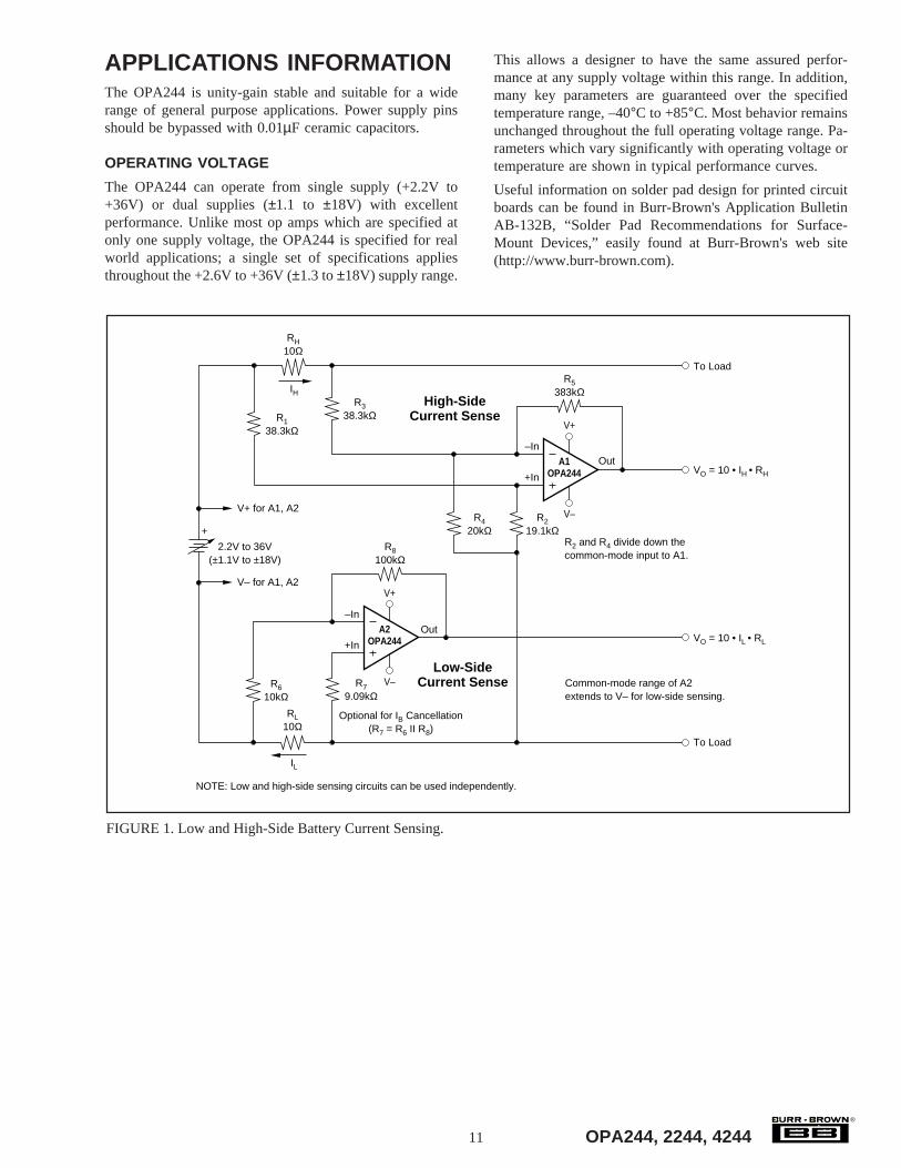
APPLICATIONS INFORMATIONThe OPA244 is unity-gain stable and suitable for a widerange of general purpose applications. Power supply pinsshould be bypassed with 0.01µF ceramic capacitors.
OPERATING VOLTAGE
The OPA244 can operate from single supply (+2.2V to+36V) or dual supplies (±1.1 to ±18V) with excellentperformance. Unlike most op amps which are specified atonly one supply voltage, the OPA244 is specified for realworld applications; a single set of specifications appliesthroughout the +2.6V to +36V (±1.3 to ±18V) supply range.
This allows a designer to have the same assured perfor-mance at any supply voltage within this range. In addition,many key parameters are guaranteed over the specifiedtemperature range, –40°C to +85°C. Most behavior remainsunchanged throughout the full operating voltage range. Pa-rameters which vary significantly with operating voltage ortemperature are shown in typical performance curves.
Useful information on solder pad design for printed circuitboards can be found in Burr-Brown's Application BulletinAB-132B, “Solder Pad Recommendations for Surface-Mount Devices,” easily found at Burr-Brown's web site(http://www.burr-brown.com).
FIGURE 1. Low and High-Side Battery Current Sensing.
RL10Ω
A1OPA244
+
R138.3kΩ
R338.3kΩ
R5383kΩ
R610kΩ
R79.09kΩ
R420kΩ
R219.1kΩ
A2OPA244
R8100kΩ
RH10Ω
IH
V+
V–
V+
V–
2.2V to 36V(±1.1V to ±18V)
V+ for A1, A2
–In
+In
–In
+InVO = 10 • IH • RH
To Load
To Load
VO = 10 • IL • RL
Common-mode range of A2extends to V– for low-side sensing.
Optional for IB Cancellation(R7 = R6 II R8)
R2 and R4 divide down thecommon-mode input to A1.
Low-SideCurrent Sense
High-SideCurrent Sense
Out
Out
NOTE: Low and high-side sensing circuits can be used independently.
V– for A1, A2
IL

PACKAGE OPTION ADDENDUM
www.ti.com 4-Oct-2017
Addendum-Page 1
PACKAGING INFORMATION
Orderable Device Status(1)
Package Type PackageDrawing
Pins PackageQty
Eco Plan(2)
Lead/Ball Finish(6)
MSL Peak Temp(3)
Op Temp (°C) Device Marking(4/5)
Samples
OPA2244EA/250 ACTIVE VSSOP DGK 8 250 Green (RoHS& no Sb/Br)
CU NIPDAU |CU NIPDAUAG
Level-2-260C-1 YEAR -40 to 85 A44
OPA2244EA/250G4 ACTIVE VSSOP DGK 8 250 Green (RoHS& no Sb/Br)
CU NIPDAUAG Level-2-260C-1 YEAR -40 to 85 A44
OPA2244EA/2K5 ACTIVE VSSOP DGK 8 2500 Green (RoHS& no Sb/Br)
CU NIPDAU |CU NIPDAUAG
Level-2-260C-1 YEAR -40 to 85 A44
OPA2244EA/2K5G4 ACTIVE VSSOP DGK 8 2500 Green (RoHS& no Sb/Br)
CU NIPDAUAG Level-2-260C-1 YEAR -40 to 85 A44
OPA2244PA ACTIVE PDIP P 8 50 Green (RoHS& no Sb/Br)
CU NIPDAU N / A for Pkg Type OPA2244PA
OPA2244PAG4 ACTIVE PDIP P 8 50 Green (RoHS& no Sb/Br)
CU NIPDAU N / A for Pkg Type OPA2244PA
OPA2244UA ACTIVE SOIC D 8 75 Green (RoHS& no Sb/Br)
CU NIPDAU Level-3-260C-168 HR OPA2244UA
OPA2244UA/2K5 ACTIVE SOIC D 8 2500 Green (RoHS& no Sb/Br)
CU NIPDAU Level-3-260C-168 HR OPA2244UA
OPA2244UA/2K5G4 ACTIVE SOIC D 8 2500 Green (RoHS& no Sb/Br)
CU NIPDAU Level-3-260C-168 HR OPA2244UA
OPA2244UAG4 ACTIVE SOIC D 8 75 Green (RoHS& no Sb/Br)
CU NIPDAU Level-3-260C-168 HR OPA2244UA
OPA244NA/250 ACTIVE SOT-23 DBV 5 250 Green (RoHS& no Sb/Br)
CU NIPDAU Level-2-260C-1 YEAR -40 to 85 A44
OPA244NA/250G4 ACTIVE SOT-23 DBV 5 250 Green (RoHS& no Sb/Br)
CU NIPDAU Level-2-260C-1 YEAR -40 to 85 A44
OPA244NA/3K ACTIVE SOT-23 DBV 5 3000 Green (RoHS& no Sb/Br)
CU NIPDAU Level-2-260C-1 YEAR -40 to 85 A44
OPA244NA/3KG4 ACTIVE SOT-23 DBV 5 3000 Green (RoHS& no Sb/Br)
CU NIPDAU Level-2-260C-1 YEAR -40 to 85 A44
OPA244UA ACTIVE SOIC D 8 75 Green (RoHS& no Sb/Br)
CU NIPDAU Level-3-260C-168 HR -40 to 85 OPA244UA
OPA244UA/2K5 ACTIVE SOIC D 8 2500 Green (RoHS& no Sb/Br)
CU NIPDAU Level-3-260C-168 HR -40 to 85 OPA244UA
OPA244UAE4 ACTIVE SOIC D 8 75 Green (RoHS& no Sb/Br)
CU NIPDAU Level-3-260C-168 HR -40 to 85 OPA244UA

PACKAGE OPTION ADDENDUM
www.ti.com 4-Oct-2017
Addendum-Page 2
Orderable Device Status(1)
Package Type PackageDrawing
Pins PackageQty
Eco Plan(2)
Lead/Ball Finish(6)
MSL Peak Temp(3)
Op Temp (°C) Device Marking(4/5)
Samples
OPA4244EA/250 ACTIVE TSSOP PW 14 250 Green (RoHS& no Sb/Br)
CU NIPDAU Level-3-260C-168 HR -40 to 85 OPA4244EA
OPA4244EA/250E4 ACTIVE TSSOP PW 14 250 Green (RoHS& no Sb/Br)
CU NIPDAU Level-3-260C-168 HR -40 to 85 OPA4244EA
OPA4244EA/2K5 ACTIVE TSSOP PW 14 2500 Green (RoHS& no Sb/Br)
CU NIPDAU Level-3-260C-168 HR -40 to 85 OPA4244EA
(1) The marketing status values are defined as follows:ACTIVE: Product device recommended for new designs.LIFEBUY: TI has announced that the device will be discontinued, and a lifetime-buy period is in effect.NRND: Not recommended for new designs. Device is in production to support existing customers, but TI does not recommend using this part in a new design.PREVIEW: Device has been announced but is not in production. Samples may or may not be available.OBSOLETE: TI has discontinued the production of the device.
(2) RoHS: TI defines "RoHS" to mean semiconductor products that are compliant with the current EU RoHS requirements for all 10 RoHS substances, including the requirement that RoHS substancedo not exceed 0.1% by weight in homogeneous materials. Where designed to be soldered at high temperatures, "RoHS" products are suitable for use in specified lead-free processes. TI mayreference these types of products as "Pb-Free".RoHS Exempt: TI defines "RoHS Exempt" to mean products that contain lead but are compliant with EU RoHS pursuant to a specific EU RoHS exemption.Green: TI defines "Green" to mean the content of Chlorine (Cl) and Bromine (Br) based flame retardants meet JS709B low halogen requirements of <=1000ppm threshold. Antimony trioxide basedflame retardants must also meet the <=1000ppm threshold requirement.
(3) MSL, Peak Temp. - The Moisture Sensitivity Level rating according to the JEDEC industry standard classifications, and peak solder temperature.
(4) There may be additional marking, which relates to the logo, the lot trace code information, or the environmental category on the device.
(5) Multiple Device Markings will be inside parentheses. Only one Device Marking contained in parentheses and separated by a "~" will appear on a device. If a line is indented then it is a continuationof the previous line and the two combined represent the entire Device Marking for that device.
(6) Lead/Ball Finish - Orderable Devices may have multiple material finish options. Finish options are separated by a vertical ruled line. Lead/Ball Finish values may wrap to two lines if the finishvalue exceeds the maximum column width.
Important Information and Disclaimer:The information provided on this page represents TI's knowledge and belief as of the date that it is provided. TI bases its knowledge and belief on informationprovided by third parties, and makes no representation or warranty as to the accuracy of such information. Efforts are underway to better integrate information from third parties. TI has taken andcontinues to take reasonable steps to provide representative and accurate information but may not have conducted destructive testing or chemical analysis on incoming materials and chemicals.TI and TI suppliers consider certain information to be proprietary, and thus CAS numbers and other limited information may not be available for release.
In no event shall TI's liability arising out of such information exceed the total purchase price of the TI part(s) at issue in this document sold by TI to Customer on an annual basis.

PACKAGE OPTION ADDENDUM
www.ti.com 4-Oct-2017
Addendum-Page 3

TAPE AND REEL INFORMATION
*All dimensions are nominal
Device PackageType
PackageDrawing
Pins SPQ ReelDiameter
(mm)
ReelWidth
W1 (mm)
A0(mm)
B0(mm)
K0(mm)
P1(mm)
W(mm)
Pin1Quadrant
OPA2244EA/250 VSSOP DGK 8 250 180.0 12.4 5.3 3.4 1.4 8.0 12.0 Q1
OPA2244EA/2K5 VSSOP DGK 8 2500 330.0 12.4 5.3 3.4 1.4 8.0 12.0 Q1
OPA2244UA/2K5 SOIC D 8 2500 330.0 12.4 6.4 5.2 2.1 8.0 12.0 Q1
OPA244NA/250 SOT-23 DBV 5 250 178.0 8.4 3.3 3.2 1.4 4.0 8.0 Q3
OPA244NA/3K SOT-23 DBV 5 3000 178.0 8.4 3.3 3.2 1.4 4.0 8.0 Q3
OPA244UA/2K5 SOIC D 8 2500 330.0 12.4 6.4 5.2 2.1 8.0 12.0 Q1
OPA4244EA/250 TSSOP PW 14 250 180.0 12.4 6.9 5.6 1.6 8.0 12.0 Q1
OPA4244EA/2K5 TSSOP PW 14 2500 330.0 12.4 6.9 5.6 1.6 8.0 12.0 Q1
PACKAGE MATERIALS INFORMATION
www.ti.com 15-Feb-2014
Pack Materials-Page 1
*All dimensions are nominal
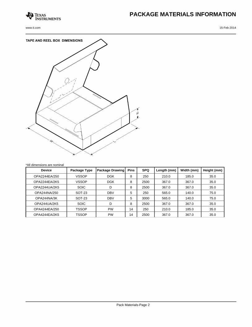
Device Package Type Package Drawing Pins SPQ Length (mm) Width (mm) Height (mm)
OPA2244EA/250 VSSOP DGK 8 250 210.0 185.0 35.0
OPA2244EA/2K5 VSSOP DGK 8 2500 367.0 367.0 35.0
OPA2244UA/2K5 SOIC D 8 2500 367.0 367.0 35.0
OPA244NA/250 SOT-23 DBV 5 250 565.0 140.0 75.0
OPA244NA/3K SOT-23 DBV 5 3000 565.0 140.0 75.0
OPA244UA/2K5 SOIC D 8 2500 367.0 367.0 35.0
OPA4244EA/250 TSSOP PW 14 250 210.0 185.0 35.0
OPA4244EA/2K5 TSSOP PW 14 2500 367.0 367.0 35.0
PACKAGE MATERIALS INFORMATION
www.ti.com 15-Feb-2014
Pack Materials-Page 2


www.ti.com
PACKAGE OUTLINE
C
TYP0.220.08
0.25
3.02.6
2X 0.95
1.9
1.45 MAX
TYP0.150.00
5X 0.50.3
TYP0.60.3
TYP80
1.9
A
3.052.75
B1.751.45
(1.1)
SOT-23 - 1.45 mm max heightDBV0005ASMALL OUTLINE TRANSISTOR
4214839/C 04/2017
NOTES: 1. All linear dimensions are in millimeters. Any dimensions in parenthesis are for reference only. Dimensioning and tolerancing per ASME Y14.5M.2. This drawing is subject to change without notice.3. Refernce JEDEC MO-178.
0.2 C A B
1
34
5
2
INDEX AREAPIN 1
GAGE PLANE
SEATING PLANE
0.1 C
SCALE 4.000

www.ti.com
EXAMPLE BOARD LAYOUT
0.07 MAXARROUND
0.07 MINARROUND
5X (1.1)
5X (0.6)
(2.6)
(1.9)
2X (0.95)
(R0.05) TYP
4214839/C 04/2017
SOT-23 - 1.45 mm max heightDBV0005ASMALL OUTLINE TRANSISTOR
NOTES: (continued) 4. Publication IPC-7351 may have alternate designs. 5. Solder mask tolerances between and around signal pads can vary based on board fabrication site.
SYMM
LAND PATTERN EXAMPLEEXPOSED METAL SHOWN
SCALE:15X
PKG
1
3 4
5
2
SOLDER MASKOPENINGMETAL UNDER
SOLDER MASK
SOLDER MASKDEFINED
EXPOSED METAL
METALSOLDER MASKOPENING
NON SOLDER MASKDEFINED
(PREFERRED)
SOLDER MASK DETAILS
EXPOSED METAL

www.ti.com
EXAMPLE STENCIL DESIGN
(2.6)
(1.9)
2X(0.95)
5X (1.1)
5X (0.6)
(R0.05) TYP
SOT-23 - 1.45 mm max heightDBV0005ASMALL OUTLINE TRANSISTOR
4214839/C 04/2017
NOTES: (continued) 6. Laser cutting apertures with trapezoidal walls and rounded corners may offer better paste release. IPC-7525 may have alternate design recommendations. 7. Board assembly site may have different recommendations for stencil design.
SOLDER PASTE EXAMPLEBASED ON 0.125 mm THICK STENCIL
SCALE:15X
SYMM
PKG
1
3 4
5
2


IMPORTANT NOTICE
Texas Instruments Incorporated (TI) reserves the right to make corrections, enhancements, improvements and other changes to itssemiconductor products and services per JESD46, latest issue, and to discontinue any product or service per JESD48, latest issue. Buyersshould obtain the latest relevant information before placing orders and should verify that such information is current and complete.TI’s published terms of sale for semiconductor products (http://www.ti.com/sc/docs/stdterms.htm) apply to the sale of packaged integratedcircuit products that TI has qualified and released to market. Additional terms may apply to the use or sale of other types of TI products andservices.Reproduction of significant portions of TI information in TI data sheets is permissible only if reproduction is without alteration and isaccompanied by all associated warranties, conditions, limitations, and notices. TI is not responsible or liable for such reproduceddocumentation. Information of third parties may be subject to additional restrictions. Resale of TI products or services with statementsdifferent from or beyond the parameters stated by TI for that product or service voids all express and any implied warranties for theassociated TI product or service and is an unfair and deceptive business practice. TI is not responsible or liable for any such statements.Buyers and others who are developing systems that incorporate TI products (collectively, “Designers”) understand and agree that Designersremain responsible for using their independent analysis, evaluation and judgment in designing their applications and that Designers havefull and exclusive responsibility to assure the safety of Designers' applications and compliance of their applications (and of all TI productsused in or for Designers’ applications) with all applicable regulations, laws and other applicable requirements. Designer represents that, withrespect to their applications, Designer has all the necessary expertise to create and implement safeguards that (1) anticipate dangerousconsequences of failures, (2) monitor failures and their consequences, and (3) lessen the likelihood of failures that might cause harm andtake appropriate actions. Designer agrees that prior to using or distributing any applications that include TI products, Designer willthoroughly test such applications and the functionality of such TI products as used in such applications.TI’s provision of technical, application or other design advice, quality characterization, reliability data or other services or information,including, but not limited to, reference designs and materials relating to evaluation modules, (collectively, “TI Resources”) are intended toassist designers who are developing applications that incorporate TI products; by downloading, accessing or using TI Resources in anyway, Designer (individually or, if Designer is acting on behalf of a company, Designer’s company) agrees to use any particular TI Resourcesolely for this purpose and subject to the terms of this Notice.TI’s provision of TI Resources does not expand or otherwise alter TI’s applicable published warranties or warranty disclaimers for TIproducts, and no additional obligations or liabilities arise from TI providing such TI Resources. TI reserves the right to make corrections,enhancements, improvements and other changes to its TI Resources. TI has not conducted any testing other than that specificallydescribed in the published documentation for a particular TI Resource.Designer is authorized to use, copy and modify any individual TI Resource only in connection with the development of applications thatinclude the TI product(s) identified in such TI Resource. NO OTHER LICENSE, EXPRESS OR IMPLIED, BY ESTOPPEL OR OTHERWISETO ANY OTHER TI INTELLECTUAL PROPERTY RIGHT, AND NO LICENSE TO ANY TECHNOLOGY OR INTELLECTUAL PROPERTYRIGHT OF TI OR ANY THIRD PARTY IS GRANTED HEREIN, including but not limited to any patent right, copyright, mask work right, orother intellectual property right relating to any combination, machine, or process in which TI products or services are used. Informationregarding or referencing third-party products or services does not constitute a license to use such products or services, or a warranty orendorsement thereof. Use of TI Resources may require a license from a third party under the patents or other intellectual property of thethird party, or a license from TI under the patents or other intellectual property of TI.TI RESOURCES ARE PROVIDED “AS IS” AND WITH ALL FAULTS. TI DISCLAIMS ALL OTHER WARRANTIES ORREPRESENTATIONS, EXPRESS OR IMPLIED, REGARDING RESOURCES OR USE THEREOF, INCLUDING BUT NOT LIMITED TOACCURACY OR COMPLETENESS, TITLE, ANY EPIDEMIC FAILURE WARRANTY AND ANY IMPLIED WARRANTIES OFMERCHANTABILITY, FITNESS FOR A PARTICULAR PURPOSE, AND NON-INFRINGEMENT OF ANY THIRD PARTY INTELLECTUALPROPERTY RIGHTS. TI SHALL NOT BE LIABLE FOR AND SHALL NOT DEFEND OR INDEMNIFY DESIGNER AGAINST ANY CLAIM,INCLUDING BUT NOT LIMITED TO ANY INFRINGEMENT CLAIM THAT RELATES TO OR IS BASED ON ANY COMBINATION OFPRODUCTS EVEN IF DESCRIBED IN TI RESOURCES OR OTHERWISE. IN NO EVENT SHALL TI BE LIABLE FOR ANY ACTUAL,DIRECT, SPECIAL, COLLATERAL, INDIRECT, PUNITIVE, INCIDENTAL, CONSEQUENTIAL OR EXEMPLARY DAMAGES INCONNECTION WITH OR ARISING OUT OF TI RESOURCES OR USE THEREOF, AND REGARDLESS OF WHETHER TI HAS BEENADVISED OF THE POSSIBILITY OF SUCH DAMAGES.Unless TI has explicitly designated an individual product as meeting the requirements of a particular industry standard (e.g., ISO/TS 16949and ISO 26262), TI is not responsible for any failure to meet such industry standard requirements.Where TI specifically promotes products as facilitating functional safety or as compliant with industry functional safety standards, suchproducts are intended to help enable customers to design and create their own applications that meet applicable functional safety standardsand requirements. Using products in an application does not by itself establish any safety features in the application. Designers mustensure compliance with safety-related requirements and standards applicable to their applications. Designer may not use any TI products inlife-critical medical equipment unless authorized officers of the parties have executed a special contract specifically governing such use.Life-critical medical equipment is medical equipment where failure of such equipment would cause serious bodily injury or death (e.g., lifesupport, pacemakers, defibrillators, heart pumps, neurostimulators, and implantables). Such equipment includes, without limitation, allmedical devices identified by the U.S. Food and Drug Administration as Class III devices and equivalent classifications outside the U.S.TI may expressly designate certain products as completing a particular qualification (e.g., Q100, Military Grade, or Enhanced Product).Designers agree that it has the necessary expertise to select the product with the appropriate qualification designation for their applicationsand that proper product selection is at Designers’ own risk. Designers are solely responsible for compliance with all legal and regulatoryrequirements in connection with such selection.Designer will fully indemnify TI and its representatives against any damages, costs, losses, and/or liabilities arising out of Designer’s non-compliance with the terms and provisions of this Notice.
Mailing Address: Texas Instruments, Post Office Box 655303, Dallas, Texas 75265Copyright © 2018, Texas Instruments Incorporated