Embed Size (px)
Citation preview

Department of Electrical and Computer Engineering
Online Control of Modular Active Power Line Conditioner
to Improve Performance of Smart Grid
Moayed Moghbel
This thesis is presented for the Degree of
Doctor of Philosophy
of
Curtin University
August 2016

ii
Declaration
To the best of my knowledge and belief, this thesis contains no material previously
published by any other person except where due acknowledgment has been made.
This thesis contains no material which has been accepted for the award of any other degree
or diploma in any university.
Signature: …M.Moghbel……………………………….
Date:……….21.08.2016………………...

iii
SYNOPSIS
Power electronic devices are growing in distribution networks, and their applications are
gaining wide attention among different users. These devices which are considered as
nonlinear loads inject harmonics to the distribution networks and thus may lead to
detrimental effects on network operation. To reduce these harmful effects, in general,
harmonic filters are introduced. Harmonic filters are designed with passive and active
configurations. Passive filters such as capacitors and inductors are simple and easy to
implement but have some disadvantages such as fixed compensation, resonance and large
sizes. On the other hand, active power filters (APFs) have smaller sizes and are able to
eliminate selected harmonics but require additional control systems for injecting non-
sinusoidal harmonic currents to eliminate the current harmonics of the nonlinear load.
However, APFs are only able to eliminate the current harmonics of nonlinear loads at
their point of common coupling (PCC) and their implementation does not guarantee the
elimination of harmonics through the entire network. Therefore, active power line
conditioners (APLCs) are introduced which are able to compensate the voltage harmonics
of the entire connected network.
Moreover, voltage instability is another issue that utilities and networks are facing.
Voltage sag or swell is a common form of voltage instability which occurs due to different
reasons such as insufficient power generation or an increase in power demand. This
phenomenon causes the network to operate very close to its minimum voltage
requirements and thus by switching large industrial loads the network voltages may go
below the limited values. A possible solution is to install a static synchronous

iv
compensator (StatCom) which is a shunt connected flexible AC transmission systems
(FACTS) device to inject or absorb reactive power to improve the network voltage profile.

v
ABSTRACT
In the recent years, along with the growing integrations of renewable power generations
and power electronic devices into the distribution networks, some serious problems such
as voltage fluctuation and harmonic distortions have ascended. These problems have
detrimental effects on power systems such as overloading, overheating and failure of
power system components and devices such as power electronic components, electric
motors, power transformers and conductors.
By controlling the reactive power and reducing harmonic distortions within transmission
and distribution networks, maximum active power flow and voltage regulation with high
power quality can be achieved. This type of compensation can be achieved by using
various topologies. Flexible AC transmission systems (FACTS) devices are used to
implement these topologies to improve the power quality.
Static synchronous compensator (StatCom) is one of the shunt FACTS devices which is
able to generate or absorb reactive current in order to control the reactive power of the
network. The ability of StatCom to improve voltage profile of the entire network is
explored in this thesis.
Active power filter (APF) is the most commonly used devices to compensate harmonic
distortions at the terminals of the nonlinear loads. APFs are designed to compensate 100%
of the nonlinear load's harmonics and improve the power quality of power systems.
However, this approach requires one APF for each nonlinear load which is may not be a
practical solution for networks with many nonlinear devices. Therefore, active power line
conditioners (APLCs) have been proposed to reduce the harmonic current contamination
of the entire network according to the power quality standards such as the IEEE 519-1992.

vi
APLC is an advanced shunt active filter which can limit the voltage total harmonic
distortion (THDv) of the entire network or a designated area below 5% as recommended
by most power quality standards.
Most of the researches are based on compensating of either reactive power flow or
harmonic distortions of the network. Furthermore, there is a research gap in design and
implementation of APLCs with the consideration of harmonic couplings, which is an
inherent characteristic of most realistic nonlinear loads and distorted networks.
The main aims of this thesis are:
1) Optimal siting and sizing of multiple APLCs in distorted smart grid (SG) networks
to control the network THDv without and with the consideration of harmonic
couplings. This is done by implementing two particle swarm optimization (PSO)
algorithms that rely on the transmitted online smart meter data including the bus
voltage profiles.
2) Simultaneous compensation of the network fundamental voltage fluctuations
(reactive power compensation) and network voltage harmonic distortions by optimal
siting and sizing of advanced APLC units with both StatCom and APF functions. This
is done by modifying the two PSO algorithms to also include reactive power
compensation at the fundamental frequency.
Detailed simulations are performed in Matlab/Simulink to first find the optimal locations
and sizes of the APLCs in a 15-bus network with six nonlinear loads (without and with
consideration of harmonic couplings) and then investigate their performance and
effectiveness in online compensation of both fundamental reactive power and harmonic
distortions (Chapter 4).

vii
ACKNOWLEDGMENTS
I am heartily thankful to my supervisor, Professor Mohammad A.S. Masoum, whose
encouragement, supervision and support from the preliminary to the concluding level
enabled me to develop an understanding of the subject and completion of my thesis. It is
a pleasure to thank my co-supervisor, Dr. Sara Deilami for her advice, supports and
guidance throughout my research. I would also like to express my gratitude to Professor
Masoum’s HDR (higher degree by research) group at Curtin University for their
contribution, help and support during the completion of the project.
I also offer my regards and blessings to my beloved family who gave me their inseparable
moral support, encouragement and prayers to the end of my education.

viii
ABBREVIATIONS
AC: Alternating-current
AHCC: Adaptive hysteresis current control
APF: Active power filter
APLC: Active power line conditioner
CMC: Cascaded multilevel converter
CSC: Current source converter
DC: Direct-current
DCMC: Diode-clamped multilevel converter
DG: Distributed generation
D-StatCom: Distribution StatCom
DVR: Dynamic voltage regulator
FACTS: Flexible AC transmission systems
FC: Fixed shunt capacitor
FCMC: Flying capacitor multilevel converter
FL-NPC: Five level neutral-point clamped
FR: Fixed shunt reactor
GTO: Gate turned-off thyristor
HCC: Hysteresis current control
HYS-PWM: Hysteresis control PWM
IEC: International electrotechnical commission
IEEE: Institute of electrical and electronics engineers
ix
IGBT: Insulated gate bipolar transistor
IGCT: Integrated gate-commutated thyristor
IPFC: Interline power flow controller
LCC: Line commutated converter compensator
MSC: Mechanical switched shunt capacitor
MSR: Mechanical switched shunt reactor
PCC: Point of common coupling
PLL: Phase-locked loop
PSO: Particle swarm optimization
SCC: Self-commutated compensator
SG: Smart grid
SGCC: Smart grid central control
SH-PWM: Selective harmonic elimination PWM
SPWM: Sinusoidal PWM
SSSC: Synchronous series compensator
StatCom: Static synchronous compensator
SVC: Static VAR compensator
SVC: Static VAR compensator
SV-PWM: Space vector PWM
TCBR: Thyristor controlled braking resistors
TCPR: Thyristor controlled phase angle regulator
TCPST: Thyristor controlled phase shifting transformers
TCR: Thyristor controlled reactor

x
TCSC: Thyristor controlled series compensator capacitor
TCSR: Thyristor controlled series compensator reactor
THDv: Voltage total harmonic distortion
TSC: Thyristor switched capacitor
TSR: Thyristor switched reactor
TSSC: Thyristor switched series compensator capacitor
TSSR: Thyristor switched series compensator reactors
UPFC: Unified power flow controller
UPQC: Universal power quality conditioner
UPS: Uninterrupted power supply
VSC: Voltage source converter

xi
Contents
List Of Figures ............................................................................................................... xvi
List Of Tables ................................................................................................................. xxi
CHAPTER 1: INTRODUCTION .................................................................................... 1
1.1 Research Objectives ........................................................................................... 6
1.2 Thesis Contributions .......................................................................................... 8
1.3 Thesis Outline .................................................................................................... 9
CHAPTER 2: FACTS DEVICES IN SMART GRIDS .................................................. 10
2.1 Smart Grid ........................................................................................................ 10
2.1.1 What is Smart Grid ................................................................................... 11
2.1.2 Benefits of Smart Grid .............................................................................. 12
2.2 Facts Devices ................................................................................................... 13
2.3 Control Methods of Shunt Converters for FACTS Applications ..................... 19
2.3.1 Sinusoidal PWM (SPWM) ........................................................................ 19
2.3.2 Space Vector PWM (SV-PWM) ............................................................... 20
2.3.3 Selective Harmonic Elimination PWM (SH-PWM) ................................. 23
2.3.4 Hysteresis Band PWM (HYS-PWM)........................................................ 23
2.4 Multilevel Power Converters ........................................................................... 24
2.4.1 Multilevel Power Converter Structures ..................................................... 25
2.4.1.1 Diode-Clamped Multilevel Converter..................................................... 25
2.4.1.2 Flying Capacitor Multilevel Converter ................................................... 27
2.4.1.3 Cascaded Multilevel Converters with Separated DC Sources ................ 28
2.4.2 Comparison among Multilevel Converters ............................................... 30

xii
2.4.3 Asymmetric Multilevel Converters ........................................................... 32
2.5 StatCom ............................................................................................................ 34
2.5.1 Comparison of SVC and StatCom ............................................................ 38
2.6 Harmonics as a Power Quality Problem .......................................................... 39
2.6.1 Harmonic Sources ..................................................................................... 40
2.6.2 Effects of Harmonics ................................................................................ 40
2.7 Harmonic Mitigation Techniques .................................................................... 41
2.7.1 Passive Harmonic Filters........................................................................... 42
2.7.2 Active Filters ............................................................................................. 43
2.7.3 Harmonic Current Extraction Techniques ................................................ 46
2.7.4 APLC ........................................................................................................ 47
CHAPTER 3: REACTIVE POWER COMPENSATION USING STATCOM ............. 50
3.1 StatCom as a Shunt Connected FACTS Device .............................................. 50
3.1.1 The Principle of StatCom .......................................................................... 51
3.1.3 Simulation Results of StatCom in Distribution System of Fig. 3.3 .......... 54
3.1.3.1 Case 3-A: Compensation of StatCom in Voltage Sag Conditions .......... 54
3.1.3.2 Case 3-B: Compensation of StatCom in Voltage Swell Conditions ....... 57
3.1.3.3 Case 3-C: Compensation of StatCom in Short-circuit Conditions ......... 59
3.2 Siting and Sizing of StatCom in Balanced and Unbalanced Distribution Networks
60
3.2.1 Particle Swarm Optimization Method ....................................................... 61
3.2.2 Problem Formulation of Siting and Sizing of StatCom ............................ 62
3.2.3 System Specifications of 15-Bus Test System .......................................... 63

xiii
3.2.4 Three-Phase StatCom with Five-Level NPC Inverter ............................... 65
3.2.4.1 Adaptive Hysteresis Current Control Design .......................................... 65
3.2.4.2 Selection of Hysteresis Band Shape ........................................................ 67
3.2.5 Simulation Results of Siting and Sizing of StatCom in Distribution Network
............................................................................................................................ 69
3.2.5.1 Case 3-D: Balanced System Operation without StatCom ....................... 69
3.2.5.2 Case 3-E: Siting and Sizing of StatComs in Balanced System ............... 70
3.2.5.3 Case 3-F: Siting and Sizing of StatComs with an Additional Constraint for
Maximum Size of StatComs (0.15 pu) in Balanced System ............................... 70
3.2.5.4 Case 3-G: Siting and Sizing of StatComs with an Additional Constraint for
Maximum Size of StatComs (0.10 pu) in Balanced System ............................... 70
3.2.5.5 Cases 3-H and 3-J; Unbalanced System Operation without StatCom .... 73
3.2.5.6 Cases 3-I and 3-K; Siting and Sizing of StatComs in an Unbalanced
Network ............................................................................................................... 73
CHAPTER 4: OPTIMAL SITING AND SIZING OF MULTIPLE APLCs FOR
FUNDAMENTAL AND HARMONIC VOLTAGE COMPENSATION ...................... 77
4.1 Modelling for Optimal Siting and Sizing of APLC for Fundamental and Harmonic
Voltage Compensation .................................................................................. 78
4.2 Optimal Online Operation of APLCs for Fundamental and Harmonic Voltage
Compensation ............................................................................................... 80
4.3 Simulation Results ........................................................................................... 82
4.3.1 System Operation without APLCs (Case 4-A) ......................................... 83

xiv
4.3.2 Optimal Siting and Sizing of Multiple APLCs (Case 4-B) for Fundamental and
Harmonic Voltage Compensation ...................................................................... 85
4.3.2.1 The Impact of Objective Function Weighting Factors on Optimal Siting and
Sizing of APLCs (Case 4-C) .............................................................................. 86
4.3.3 Optimal Siting and Sizing of Multiple APLCs for Fundamental and Harmonic
Voltage Compensation with an Additional Constraint for Maximum Size of APLCs
of 0.15 pu (Case 4-D) ......................................................................................... 93
4.3.4 Optimal Siting and Sizing of Multiple APLCs for Fundamental and Harmonic
Voltage Compensation with an Additional Constraint for Maximum Size of APLCs
of 0.10 pu (Case 4-E) ......................................................................................... 95
4.3.5 Optimal Online Operation of the Allocated APLCs (Case 4-F) for Fundamental
and Harmonic Voltage Compensation ............................................................... 96
CHAPTER 5: IMPACTS OF HARMONIC COUPLINGS ON OPTIMAL SITING,
SIZING AND ONLINE CONTROL OF MULTIPLE APLCs .................................... 103
5.1 Nonlinear Modeling and Control of APLCs .................................................. 103
5.2 Optimal Online Operation of APLCs Considering Harmonic Couplings ...... 106
5.3 Simulations for Optimal Siting/Sizing of APLCs with Considering Harmonic
Couplings .................................................................................................... 107
5.3.1 Case 5-A: System Operation without APLCs ......................................... 108
5.3.2 Case 5-B: Optimal Siting and Sizing of Multiple APLCs without Considering
the Maximum APLC Size ................................................................................ 110
5.3.3 Case 5-C: Impacts of Maximum APLC Size (Imax) on Optimal Siting and Sizing
Solution ............................................................................................................ 112

xv
5.3.4 Case 5-D: Optimal Siting and Sizing of Multiple APLCs with Imax = 0.07pu
.......................................................................................................................... 114
5.4. Simulations for Optimal Operation of the Allocated APLCs ....................... 115
5.4.1. Case 5-E: System Operation with the Four Optimal APLC Locations and Sizes
of Cases 5-D1 and 5-D2 ................................................................................... 116
5.4.2. Case 5-F: Online Operation and Control of APLCs Considering Harmonic
Couplings ......................................................................................................... 118
CHAPTER 6: CONCLUSION .................................................................................... 122
6.1 6.1 Recommendations and Future Research Directions ............................. 126
REFERENCES .............................................................................................................. 128

xvi
LIST OF FIGURES
FIGURE 2.1: SHUNT FACTS DEVICES WITH; (A) VCS, (B) CSC [31] ................................ 15
FIGURE 2.2: FACTS DEVICE CONNECTION TOPOLOGIES; (A) SHUNT, (B) SERIES, (C) SERIES-
SHUNT [32] ............................................................................................................... 16
FIGURE 2.3: FACTS DEVICE BUILDING BLOCKS; (A) TSR/TCR, (B) TSC, (C) TCSR/TSSR,
(D) TCSC/TSSC [31] ............................................................................................... 18
FIGURE 2.4: FACTS DEVICES BASED ON DIFFERENT CONNECTION TOPOLOGIES [31] ....... 19
FIGURE 2.5: THREE-PHASE VOLTAGE SOURCE PWM INVERTER [33] ................................ 21
FIGURE 2.6: THE BASIC SWITCHING VECTORS AND SECTORS [33] ..................................... 22
FIGURE 2.7: SPACE VECTOR CONTROL FOR SHUNT FACTS DEVICES [32] ........................ 23
FIGURE 2.8: THREE-PHASE FIVE-LEVEL DCMC [80] ........................................................ 26
FIGURE 2.9: THREE-PHASE FIVE-LEVEL FCMC [80] ........................................................ 28
FIGURE 2.10: THREE-PHASE (2N+1)-LEVEL CMC [80] .................................................... 29
FIGURE 2.11: NUMBER OF COMPONENTS REQUIRED IN THE MULTILEVEL CONVERTERS AS A
FUNCTION OF THE NUMBER OF VOLTAGE LEVELS [80] .............................................. 31
FIGURE 2.12: THREE-PHASE ASYMMETRIC MULTILEVEL CONVERTER [109] ..................... 33
FIGURE 2.13: DIFFERENT CONTROL TECHNIQUES FOR MULTILEVEL CONVERTERS [69] .... 33
FIGURE 2.14: EQUIVALENT CIRCUIT DIAGRAM OF STATCOM [33] .................................... 39
FIGURE 2.15: APF; (A) THREE-PHASE CIRCUIT DIAGRAM, (B) VOLTAGE AND CURRENT
WAVEFORMS BEFORE AND AFTER CONNECTION OF APF ........................................... 44
FIGURE 2.16: DVR CIRCUIT DIAGRAM [124] .................................................................... 44
FIGURE 2.17: THREE-PHASE THREE WIRE UPQC [128] .................................................... 45

xvii
FIGURE 2.18: SINGLE LINE DIAGRAM OF APF CONNECTED TO THE DISTRIBUTION NETWORK
................................................................................................................................. 46
FIGURE 2.19: HARMONIC EXTRACTION TECHNIQUES [132] .............................................. 47
FIGURE 2.20: SINGLE LINE DIAGRAM OF APLC CONNECTED TO DISTRIBUTION SYSTEM .. 48
FIGURE 2.21: THREE-PHASE ASYMMETRIC CMC APLC CONNECTED TO THE GRID [109] 49
FIGURE 3.1 : STATCOM PRINCIPLE DIAGRAM; (A) POWER CIRCUIT, (B) REACTIVE POWER
EXCHANGE [34] ........................................................................................................ 52
FIGURE 3.2: EQUIVALENT CIRCUIT OF STATCOM [33] ...................................................... 53
FIGURE 3.3: THE SIMULATED DISTRIBUTION NETWORK WITH STATCOM FOR CASES 3-A TO
3-C [33] ................................................................................................................... 54
FIGURE 3.4: SIMULATION RESULTS FOR CASE 3-A; (A) NETWORK LINE VOLTAGE, (B)
INJECTED ACTIVE AND REACTIVE POWER OF STATCOM, (C) STATCOM INJECTED
CURRENT. ................................................................................................................. 56
FIGURE 3.5: SIMULATION RESULTS FOR CASE 3-B; (A) NETWORK LINE VOLTAGE, (B)
INJECTED ACTIVE AND REACTIVE POWER OF STATCOM, (C) VOLTAGE AND CURRENT OF
STATCOM ................................................................................................................. 58
FIGURE 3.6: SIMULATION RESULTS FOR CASE 3-C; (A) NETWORK LINE VOLTAGE, (B)
INJECTED ACTIVE AND REACTIVE POWER OF STATCOM, (C) STATCOM INJECTED
CURRENT .................................................................................................................. 60
FIGURE 3.7: THE 15-BUS TEST SYSTEM [139] INCLUDING LOCAL LOADS AND FOUR LARGE
LOADS ...................................................................................................................... 64
FIGURE 3.8: DETAILED FL-NPC INVERTER STRUCTURE OF THE SHUNT FACTS DEVICES
[140] ........................................................................................................................ 66

xviii
FIGURE 3.9: THE APLC GENERATED FL-NPC INVERTER VOLTAGE USING HCC; (A) IDEAL
(BLUE) AND ACTUAL (RED) WAVEFORMS, (B)-(E) DETAILED WAVEFORMS FOR AREAS 1
TO 4 [140]: ............................................................................................................... 68
FIGURE 3.10: HYSTERESIS-SHAPE SELECTION ACCORDING TO EQS. 3.13-3.14 [140]: ....... 69
FIGURE 3.11: SIMULATION RESULTS OF STATCOM IN THE BALANCED NETWORK; (A) |V| OF
BUSES FOR A NETWORK OF FIG. 3.7 FOR CASES 3-D TO 3-G, (B) INJECTED CURRENT OF
STATCOM AT BUS 4 FOR CASE 3-G, (C) VOLTAGE PROFILE OF BUS 13 WITH AND
WITHOUT STATCOM FOR CASE 3-G .......................................................................... 72
FIGURE 3.12: |V| OF ALL BUSES FOR CASES 3-I AND 3-K SIMULATION IN UNBALANCED
NETWORK OF FIG 3.7 ................................................................................................ 75
FIGURE 3.13: SIMULATION RESULTS OF STATCOM IN UNBALANCED NETWORK OF FIG 3.7;
(A) VOLTAGE PROFILE OF BUS 13 WITH AND WITHOUT STATCOMS FOR CASES 3H TO 3-
K, (B) INJECTED CURRENT OF STATCOM AT BUS 3 FOR CASES 3-I AND 3-K, (C) INJECTED
CURRENT OF STATCOM AT BUS 13 FOR CASES 3-I AND 3-K ...................................... 76
FIGURE 4.1: FLOWCHART OF THE PROPOSED PSO ALGORITHM FOR FUNDAMENTAL AND
HARMONIC VOLTAGE COMPENSATION; (A) OPTIMAL SITING AND SIZING OF MULTIPLE
APLCS BASED ON EQS. 4.1-4.5, (B) OPTIMAL ONLINE CONTROL OF THE INSTALLED
APLCS BASED ON EQS. 4.3-4.7 ................................................................................ 81
FIGURE 4.2: SINGLE-LINE DIAGRAM OF THE 15-BUS DISTORTED SYSTEM [139] WITH SIX
NONLINEAR LOADS (TABLES 3.1-3.2) ....................................................................... 82
FIGURE 4.3: SIMULATION RESULTS FOR CASE 4-A (OPERATION OF THE NETWORK IN FIG. 4.2
WITHOUT ANY APLCS, TABLE 4.2) .......................................................................... 83
FIGURE 4.4: SIMULATION RESULTS FOR CASE 4-B (TABLE 4.3) ....................................... 86

xix
FIGURE 4.5: IMPACT OF THE OBJECTIVE FUNCTION WEIGHTING FACTORS (EQ. 4.2) ON
OPTIMAL APLC SITING AND SIZING SOLUTIONS ....................................................... 89
FIGURE 4.6: IMPACT OF THE OBJECTIVE FUNCTION WEIGHTING FACTORS (EQ. 4.2) ON
VOLTAGE PROFILE OF BUS 13 ON A NETWORK OF FIG. 4.2 ........................................ 89
FIGURE 4.7: SIMULATION RESULTS FOR CASE 4-D (TABLE 4.11) ..................................... 94
FIGURE 4.8: SIMULATION RESULTS FOR CASE 4-E (TABLE 4.12)...................................... 96
FIGURE 4.9: LINE DIAGRAM OF THE THREE-PHASE 15-BUS DISTORTED SYSTEM [139] IN
MATLAB/SIMULINK WITH SIX NONLINEAR LOADS (TABLES 3.1 AND 3.2) ................. 99
FIGURE 4.10: VOLTAGE WAVEFORM OF BUS 13 BEFORE (RED LINE) AND AFTER (BLUE LINE)
OPERATION OF APLCS ............................................................................................. 99
FIGURE 4.11: THE THDV PROFILES OF ALL BUSES FOR THE OPTIMAL ONLINE OPERATION OF
THE 15-BUS NETWORK OF FIG. 4.2 FOR CASES 4-F4 TO 4-F1 .................................. 100
FIGURE 4.12: THE VFUND PROFILES OF ALL BUSES FOR THE OPTIMAL ONLINE OPERATION OF
THE 15-BUS NETWORK OF FIG. 4.2 FOR CASES 4-F4 TO 4-F1 .................................. 100
FIGURE 4.13: OPTIMAL ONLINE OPERATION OF THE 15-BUS NETWORK OF FIG. 4.2 FOR CASES
4-F4 TO 4-F1; (A) MAGNITUDE OF APLC INJECTED CURRENTS AT BUS 13, (B) THE
APLC INJECTED CURRENTS WAVEFORM AT BUS 13 ................................................ 101
FIGURE 5.1: FLOWCHART OF THE PROPOSED PSO ALGORITHMS WITH CONSIDERING
HARMONIC COUPLINGS; (A) OPTIMAL SITING AND SIZING OF MULTIPLE APLCS BASED
ON EQS. 4.4-4.5 AND 5.2-5.3, (B) OPTIMAL ONLINE CONTROL OF THE INSTALLED
APLCS BASED ON EQS. 5.1, 4.4-4.5 AND 5.4-5.5 ................................................... 105
FIGURE 5.2: SIMULATION RESULTS FOR CASE 5-A; (A) CASE 5-A1, (B) CASE 5-A2, (C)
COMPARING THDV OF ALL BUSES FOR CASES 5-A1AND 5-A2 ............................... 110

xx
FIGURE 5.3: SIMULATION RESULTS FOR CASE 5-B; (A) CASE 5-B1, (B) CASE 5-B2 ....... 112
FIGURE 5.4: SIMULATION RESULTS FOR CASE 5-D; (A) CASE 5-D1, (B) CASE 5-D2 ....... 115
FIGURE 5.5: SIMULINK THREE-PHASE 15-BUS DISTORTED SYSTEM [139] LINE DIAGRAM IN
MATLAB/SIMULINK WITH SIX NONLINEAR LOADS (TABLES 3.1 AND 3.2) CONSIDERING
HARMONIC COUPLINGS ........................................................................................... 119
FIGURE 5.6: OPTIMAL ONLINE OPERATION OF THE 15-BUS NETWORK OF FIG. 4.2 (USING THE
SECOND PSO ALGORITHM OF FIG. 5.1B CONSIDERING HARMONIC COUPLINGS (TABLE
5.1, ROWS 3-5)) FOR CASES 5-E1 TO 5-E4 WITH FOUR APLCS AT BUSES 4, 6, 9 AND 12;
(A) THE APLC INJECTED CURRENTS AT BUS 13, (B) THDV OF ALL BUSES, (C) ZOOMED
WAVEFORM OF FIG. 5.6A ........................................................................................ 120

xxi
LIST OF TABLES
TABLE 2.1: EIGHT INVERTER VOLTAGE VECTORS (V0-V7) .............................................. 21
TABLE 2.2: FIVE-LEVEL INVERTER VOLTAGE LEVELS OF DCMC WITH CORRESPONDING
SWITCH STATES ........................................................................................................ 27
TABLE 2.3: SWITCH COMBINATIONS OF FIVE-LEVEL FCMC VOLTAGE LEVELS AND THEIR
CORRESPONDING SWITCH STATES ............................................................................. 28
TABLE 2.4: COMPARISON OF POWER COMPONENT REQUIREMENTS PER PHASE LEG AMONG
THREE MULTILEVEL CONVERTERS ............................................................................ 31
TABLE 2.5: HARMONIC VOLTAGE LIMITS (IEEE STD. 519-1992) [38] ............................. 41
TABLE 2.6: HARMONIC CURRENT LIMITS FOR GENERAL DISTRIBUTION SYSTEMS (IEEE STD.
519-1992) [38] ......................................................................................................... 41
TABLE 3.1: LINE DATA OF THE NETWORK IN FIG. 3.7 ....................................................... 64
TABLE 3.2: LINEAR LOAD DATA OF THE NETWORK IN FIG. 3.11 ....................................... 64
TABLE 3.3: CASES 3-D TO 3-G; OPERATION OF THE NETWORK IN FIG. 3.7 WITH AND
WITHOUT STATCOM IN BALANCED SYSTEM .............................................................. 71
TABLE 3.4: CASES 3-H AND 3-I; OPERATION OF THE NETWORK IN FIG. 3.7 WITH AND
WITHOUT STATCOM IN UNBALANCED SYSTEM ......................................................... 74
TABLE 3.5: CASES 3-J AND 3-K: OPERATION OF THE NETWORK IN FIG. 3.7 WITH AND
WITHOUT STATCOM IN UNBALANCED SYSTEM ......................................................... 75
TABLE 4.1: CURRENT HARMONIC INJECTION OF THE NONLINEAR LOADS (IN PERCENTAGE OF
THE FUNDAMENTAL COMPONENT) IN THE NETWORK OF FIG. 4.2 .............................. 83
TABLE 4.2: CASE 4-A; OPERATION OF THE NETWORK IN FIG. 4.2 WITHOUT ANY APLCS . 84

xxii
TABLE 4.3: CASE 4-B; OPTIMAL SITING AND SIZING OF MULTIPLE APLCS FOR THE
NETWORK OF FIG. 4.2 FOR FUNDAMENTAL AND HARMONIC VOLTAGE COMPENSATION
................................................................................................................................. 85
TABLE 4.4: CASE 4-C; IMPACT OF THE OBJECTIVE FUNCTION WEIGHTING FACTORS (EQ. 4.2)
ON OPTIMAL APLC SITING AND SIZING SOLUTIONS .................................................. 88
TABLE 4.5: OPTIMAL SITING AND SIZING OF MULTIPLE APLCS FOR THE NETWORK OF FIG.
4.2 FOR WTHD = 0, WSIZE = 1 AND WITHOUT CONSTRAINT ON MAXIMUM APLC
CURRENT (CASE 4-C1) ............................................................................................. 90
TABLE 4.6: OPTIMAL SITING AND SIZING OF MULTIPLE APLCS FOR THE NETWORK OF FIG.
4.2 FOR WTHD = 0.2, WSIZE = 0.8 AND WITHOUT CONSTRAINT ON MAXIMUM APLC
CURRENT (CASE 4-C2) ............................................................................................. 90
TABLE 4.7: OPTIMAL SITING AND SIZING OF MULTIPLE APLCS FOR THE NETWORK OF FIG.
4.2 FOR WTHD = 0.4, WSIZE = 0.6 AND WITHOUT CONSTRAINT ON MAXIMUM APLC
CURRENT (CASE 4-C3) ............................................................................................. 91
TABLE 4.8: OPTIMAL SITING AND SIZING OF MULTIPLE APLCS FOR THE NETWORK OF FIG.
4.2 FOR WTHD = 0.6, WSIZE = 0.4 AND WITHOUT CONSTRAINT ON MAXIMUM APLC
CURRENT (CASE 4-C5) ............................................................................................. 91
TABLE 4.9: OPTIMAL SITING AND SIZING OF MULTIPLE APLCS FOR THE NETWORK OF FIG.
4.2 FOR WTHD = 0.8, WSIZE = 0.2 AND WITHOUT CONSTRAINT ON MAXIMUM APLC
CURRENT (CASE 4-C6) ............................................................................................. 92
TABLE 4.10: OPTIMAL SITING AND SIZING OF MULTIPLE APLCS FOR THE NETWORK OF FIG.
4.2 FOR WTHD = 1, WSIZE = 0 AND WITHOUT CONSTRAINT ON MAXIMUM APLC
CURRENT (CASE 4-C7) ............................................................................................. 92

xxiii
TABLE 4.11: CASE 4-D; OPTIMAL SITING AND SIZING OF MULTIPLE APLCS CONSIDERING A
MAXIMUM APLC CURRENT OF 0.15 PU FOR THE NETWORK OF FIG. 4.2 FOR
FUNDAMENTAL AND HARMONIC VOLTAGE COMPENSATION (WTHD = 0.5, WSIZE = 0.5)
................................................................................................................................. 93
TABLE 4.12: CASE 4-E; OPTIMAL SITING AND SIZING OF MULTIPLE APLCS CONSIDERING A
MAXIMUM APLC CURRENT OF 0.10 PU FOR THE NETWORK OF FIG. 4.2 FOR
FUNDAMENTAL AND HARMONIC VOLTAGE COMPENSATION (WTHD = 0.5, WSIZE = 0.5)
................................................................................................................................. 95
TABLE 4.13: CASE 4-F; SYSTEM OPERATION WITH DIFFERENT NUMBERS OF
SIMULTANEOUSLY ACTIVATED NONLINEAR LOADS AND APLCS AS ALLOCATED AND
SIZED IN CASES 4-D FOR FUNDAMENTAL AND HARMONIC VOLTAGE COMPENSATION
(WTHD = 0.5, WSIZE = 0.5) ......................................................................................... 98
TABLE 5.1: CURRENT HARMONIC INJECTION OF THE NONLINEAR LOADS (IN PERCENTAGE OF
THE FUNDAMENTAL COMPONENT) IN THE NETWORK OF FIG.4.2 ............................. 107
TABLE 5.2: SIMULATED CASE STUDIES FOR THE DISTORTED 15-BUS NETWORK OF FIG.4.2
WITH CONSIDERING HARMONIC COUPLINGS ............................................................ 108
TABLE 5.3: CASE 5-A; OPERATION OF THE NETWORK IN FIG.4.2 WITHOUT ANY APLCS 109
TABLE 5.4: CASE 5-B; OPTIMAL SITING AND SIZING OF MULTIPLE APLCS (THE FIRST PSO
ALGORITHM OF FIG. 5.1A AND NOT CONSIDERING A MAXIMUM APLC SIZE) .......... 111
TABLE 5.5: CASE 5-C; IMPACT OF MAXIMUM APLC SIZE ON THE OPTIMAL SITING AND
SIZING SOLUTION .................................................................................................... 113
TABLE 5.6: CASE 5-D; OPTIMAL SITING AND SIZING OF MULTIPLE APLCS CONSIDERING A
MAXIMUM APLC CURRENT OF 0.07PU (TABLE 5.5, ROW 9) ................................... 114

xxiv
TABLE 5.7: CASE 5-E; SYSTEM OPERATION WITH THE FOUR OPTIMALLY LOCATED/SIZED
APLCS OF CASE 5-D1 AND 5-D2 (TABLE 5.6, COLUMNS 8 AND 15) CONSIDERING A
DIFFERENT NUMBER OF NONLINEAR LOADS. PURPLE CELLS INDICATE UNACCEPTABLE
THDV LEVELS CAUSED BY THE INACCURATE SITING/SIZING OF CASE 5-D2 DUE TO THE
IGNORANCE OF HARMONIC COUPLINGS ................................................................... 117

1
CHAPTER 1: INTRODUCTION
At the beginning of using electrical power networks, the power generation was in direct-
current (DC) forms and hence there were no changes in voltage levels due to lack of using
transformers. Therefore, the loads were located very close to generation to prevent voltage
drops. Due to disadvantages of using DC power generations and also a lack of power
electronic device technologies, alternating-current (AC) power systems relying on power
transformers were firstly introduced by Nikola Tesla by the end of the 1800s. Therefore,
the different voltage levels were introduced by implementing AC power systems
combined with power transformers.
Later smart grids were introduced as a new paradigm to change fundamentally the way
electrical energy is delivered and consumed. Although the details, configurations and
standards of smart grids are yet to be finalized, it is clear that a high-speed bi-directional
communication networks will be included as the backbone of the infrastructure. This will
provide opportunities for online and real-time monitoring and control of transmission,
distribution and end-user consumer assets for more effective coordination and usage of
the available energy resources.
Recently, there has been substantial interest in reactive power as one of several
supplementary services required for the reliability of the power systems due to its vital
effect on power system security. Power electronic devices are becoming more popular
and their applications are growing in power systems and specially in distribution networks
and gaining wide attention among different users. They are extensively engaged to control
a wide range of electrical active and passive loads such as variable speed drives,

2
uninterrupted power supply (UPS) and electric furnaces. These nonlinear loads draw
harmonic currents and reactive power as well as active power from the main AC sources.
The harmonic distortions were noticed in 1920s due to the telephone line interferences.
Since then various standards are introduced to set the limits on magnitudes of harmonic
currents and voltages. Some institutes such as International Electrotechnical Commission
(IEC) and Institute of Electrical and Electronics Engineers (IEEE) specify the limits for
harmonic voltages [1] while others including IEEE-Industry Applications Society and
IEEE-Power Engineering Society aim to detect the effects of harmonics on power systems
and introduce standards for harmonics [2]. Three classes of residential, commercial and
distribution networks are investigated in the American Electric Power Distribution
System [3] and their harmonic levels are reported. IEEE 519-1981 includes the IEEE
standard for harmonic control and reactive compensation of static power converters [4].
There are many other activities reported regarding finding standards for harmonics in
power systems [5-12].
Reactive power is relative to bus voltage levels and deficiency of enough reactive power
supply leading to poor voltage profile with the possibility of voltage collapse within power
systems. Moreover, reactive power and harmonic components of load current reduce the
system power factor leading to an increase in transmission network losses, overheating of
devices, malfunctioning and failure of electronic components (especially protection
devices and relays), overloading, overheating and failure of power factor correction
capacitors, overheating and failure of electric motors, overloading and overheating of
distribution transformers and conductors and measurement errors in metering equipment
[3-5]. Furthermore, quick variations in reactive power consumption of large loads can

3
lead to voltage oscillations which might cause power fluctuations within the network [13-
14]. Voltage sag is a significant issue for the utilities, contributing more than 80 percent
of power quality problems in the power systems [15]. Voltage sag is defined as the RMS
reduction of the AC voltage at fundamental frequency for the duration of a half-cycle to
a few seconds [16]. Voltage swell is another kind of voltage instability which may occur
under different scenarios. For example, high penetration of photovoltaic (PV) generation
is one of the main reasons for voltage rise in the system due to reversed power flow to the
network [17-18]. There are however, some solutions to overcome the voltage rise such as
adjusting distribution transformer ratio [19-20] or reducing power line impedances by
increasing conductor sizes [21-22]. But these approaches are not able to cover all extreme
scenarios. There are some modern loads which are generally based on the electronic
devices such as programmable logic controllers (PLC). These devices are very sensitive
to voltage fluctuations and become less tolerant to power quality problems [23] including
voltage sags, swells and harmonics.
Electric power loads can be either static or dynamic [24-25]. Moreover, they can be
balanced loads such as three-phase electrical motors or unbalanced devices such as single
phase loads [26-27], traction loads [28] or arc furnaces [29]. Many loads such as induction
motors are very sensitive to voltage imbalances and even small voltage imbalances can
result in overheating and unbalanced their electromagnetic torque. Therefore, it is very
important to rectify voltage imbalances in the networks.
Generally, most of power system loads are resistive-inductive. If the inductive
characteristic of loads increases, the power factor of network decreases and forces the
utilities to inject more current in order to maintain the same level of active power [30].

4
Therefore, it is recommended to provide reactive power compensation for very high
inductive loads. The conventional compensation of reactive power is based on connecting
shunt capacitor or inductor banks to the system through mechanical switches. However,
these methods have many disadvantages such as fixed compensation, resonance, large
size and weight, as well as noise and losses. By controlling the reactive power within
transmission and distribution networks, maximum active power flow and voltage
regulation can be achieved. This type of controller can be applied by using various
topologies. Flexible AC transmission systems (FACTS) devices are used to implement
these topologies to improve the power quality [31]. The static synchronous compensator
(StatCom) is a shunt connected FACTS device capable of generating or absorbing reactive
power and can be controlled independently of the AC power system whose output can be
varied in order to maintain control of specific parameters of the electric power system
[32-34]. The StatCom is basically static and does not include any rotating parts like
synchronous condenser and hence StatCom provides quicker response than synchronous
condenser.
Therefore, in order to compensate the loads requirements, customers or utilities need to
install FACTS devices. Thus, to improve the power factor and also to achieve load
balancing, reactive power is injected into the network. As a result of implementing these
devices, even when the loads are inductive and unbalanced, the grid is balanced and very
closer to unity power factor [35].
StatCom usually generates a balanced set of three-phase sinusoidal voltages at the
fundamental frequency with controllable amplitude and phase angle. Unlike most
5
conventional reactive power compensators, StatCom facilitates dynamic compensation of
electrical power systems and improves the utilization of existing networks [36].
As mentioned above, the use of electronic devices is growing and therefore, the emergent
applications of nonlinear loads and renewable resources such as converters, variable speed
drives, smart appliances, distributed generations (DGs) and storage systems is increasing
the injected harmonic currents that will ultimately propagate in the network and create
voltage harmonics [37]. These distortions have injurious impacts on the network operation
and its components such as overheating of power transformers, motors and cables;
creating harmonic resonances; causing low power factor conditions and mal-operations
of protection devices [37]. The acceptable limits of harmonic current and voltage
distortions are provided by the power quality standards such as the IEEE-519 [38].
According standards, consumers are responsible to keep their injected harmonic current
magnitudes and current total harmonic distortion (THDi) at their point of common
couplings (PCCs) below the permissible levels while utilities are required to control the
voltage total harmonic distortion (THDv) of the network and the individual buses [37-38].
The most common approaches for improving power quality is to require the consumers
with nonlinear loads to either reduce their harmonic injections or install (passive, active
and hybrid) filters. However, these technologies are designed to limit harmonic currents
at the PCC without considering the THDv of other buses and the entire network [37].
Furthermore, restriction of injected current harmonics at PCCs within the permissible
levels (e.g., THDi<5% for short-circuit ratios<20 [38]) does not necessarily result in
acceptable bus and network voltage distortions (e.g., THDv<5% as recommended by most
standards [37-38]). There are a few options to resolve the network voltage distortion issue:

6
i) the precise compensation of all injected current harmonics by installing active power
filters (APFs [39]) at all buses with nonlinear loads which is not a practical solution, ii)
installation of universal power quality conditioners (UPQCs) at the buses with sensitive
loads that may not be efficient for large systems with many sensitive consumers, iii)
optimal siting, sizing and connection of active power line conditioners (APLCs) to limit
the network THDv.
APLCs are enhanced APFs with a few differences including [40-51]: i) they are only
installed at a few selected buses, ii) they can control THDv and percentages of individual
voltage harmonics at all buses within permissible limits, iii) instead of injecting equal-
but-opposite harmonic currents to fully compensate the nonlinear load distortions, their
reference currents are optimized to limit the overall network THDv.
While there are many publications on APFs, the research on APLCs has been very limited
[40-51] mainly due to the unavailability of online network data. However, this problem
has been recently resolved with wide spread installation of smart meters in smart grids
(SGs) with sophisticated communication networks. The research on APLCs can be
classified into optimal siting and sizing of single [40-46] and multiple [47-51] APLC
units. However, all publications on APLC siting and sizing ignore the impacts of harmonic
couplings imposed by the nonlinear devices.
1.1 Research Objectives
This thesis will first review the detrimental effects of nonlinear loads such as harmonic
distortions and voltage instability in distribution networks and then will introduce some
solutions to compensate the harmonic distortions and improve the power quality. APLC

7
with PSO-based algorithm control is introduced to compensate the voltage fundamental
and harmonic distortions and to maintain the entire network voltage profile within the
voltage and harmonic standards. The main objectives of this thesis are:
1) Optimal siting and sizing of multiple APLCs in distorted smart grid (SG) networks
to control the network THDv without and with the consideration of harmonic couplings
(Chapter 5).
2) Simultaneous compensation of the network fundamental voltage fluctuations
(reactive power compensation) and network voltage harmonic distortions by optimal
siting and sizing of advanced APLC units with both StatCom and APF functions
(Chapter 4).
To achieve these objectives, two particle swarm optimization (PSO) algorithms are first
implemented that rely on the transmitted online smart meter data including the node
voltage profiles to compensate network harmonic distortions. Then, they are modified to
also include reactive power compensation at the fundamental frequency.
Detailed simulations are performed in Matlab/Simulink to first find the optimal locations
and sizes of the APLCs in a 15-bus network with six nonlinear loads (without and with
consideration of harmonic couplings) and then investigate their performance and
effectiveness in online compensation of both fundamental reactive power and harmonic
distortions.
The main research goals are to formulate the optimal siting and sizing of APLCs problem,
define the PSO objective function and select appropriate constraints of PSO such that the
following requirements are fulfilled within a 24 hour period:
1. Limit the THDv of the entire network as well as THDv of each bus to 5%.

8
2. Limit each individual harmonic distortion of each bus to 3%.
3. Improving the voltage profile of each bus to reach the minimum magnitude voltage of
0.9 pu.
4. Optimally allocate APLCs through the network to minimize the harmonic distortions
and improve voltage profile.
5. Sizing the APLCs to achieve optimal APLC sizes.
6. Optimal operation of allocated APLCs to compensate the harmonic distortions and
improve the voltage profile of the entire network.
1.2 Thesis Contributions
In this thesis, PSO-based algorithms are proposed and implemented to improve the
performance of smart grid networks at the fundamental and harmonic frequencies. The
main contributions are:
Optimal siting and sizing of multiple APLCs in distorted SG networks to control
the network THDv.
Including of harmonic couplings in the APLC siting and sizing solution.
Extending the APLC function also to include fundamental reactive power
compensation (in addition to the harmonic current compensations) and also
improve the network voltage profiles at the fundament frequency.
The online optimal operation of multiple APLCs in SG networks with the
availability of online bus voltage data transmitted by smart meters.

9
Minimizing the THDv of each bus, the THDv of the entire network and the
individual harmonic distortion of each bus while also improving bus voltage
profiles.
1.3 Thesis Outline
This thesis is organized into six chapters. Chapter 2 gives an introduction to SGs and
FACTS devices. It highlights the importance of FACTS devices on improving voltage
profiles. It also briefly reviews some of the FACTS devices with the focus on shunt
compensation devices such as StatCom. This chapter also presents reviews on APF and
APLCs. Chapter 3 represents the StatCom modelling and confirms its ability to
compensate the reactive power to improve voltage profile. Chapter 4 demonstrates the
APLC modelling and proposes a PSO-based algorithm for APLC siting and sizing. The
algorithm is implemented in 15 bus system by finding the optimal locations of APLCs
and confirming their ability to compensate the reactive power and harmonic distortions
of the entire network. Chapter 5 develops and improves the accuracy of the PSO solutions
by also considering the effects of harmonic couplings. Finally, Chapter 6 provides the
conclusions.

10
CHAPTER 2: FACTS DEVICES IN SMART GRIDS
2.1 Smart Grid
SGs are attaining worldwide attention of interest among consumers to increase demand-
size management quality by using smart meters and sensors [52] and also improve
network efficiency and reliability [53-54].
New equipment and appliances such as computers, variable speed drives, TVs, smart
appliances, hybrid vehicles, PEVs, home area networks and other electronic devices are
occupying every home and business. These emerging demands will need new power grid
infrastructure, but will also require innovative new concepts and technologies to continue
to drive the economy forward. Most utilities believe that it is time to revisit the critical
infrastructure of the power grids and re-examine their abilities to drive our security and
prosperity for the next 100 years. In such a case, SG configurations would be the best
candidates to assure real-time information, countless choices, rapid decisions, and fast
responses.
Most industries are planning to develop SGs based on the following understandings,
concepts and requirements:
First, the appliances and equipment must be able to communicate and ultimately
support the optimal operation of the entire grid. This requires a simple but smart
interface for these devices to operate easily in alignment with the overall operational
priorities of the grid.
11
Second, consumers must also have the ability to understand grid operations and be
able to accordingly and wisely adjust their electricity consumption. Subsequently,
there should be simple interfaces between the grid and the consumer that allow them
to support the needs of the grid. Consumers must be given the chance and ability to
interact with the grid and adjust the energy consumption of their homes and businesses
in harmony with their lifestyle choices, values, and unique and variable requirements.
Third, the grid must be able to absorb easily and effectively new technologies and
systems such as solar panels, wind turbines, fuel cells, storage batteries and PEVs to
ensure a healthy growing economy.
SGs are already being created in most countries. Technologies that created the internet
and modern communication are already revolutionizing how we deliver electricity.
2.1.1 What is Smart Grid
The electric industry is to make the transformation from the conventional centralized,
producer-controlled network to the less centralized and more consumer-interactive. SG
makes this transformation possible by bringing the philosophies, concepts and
technologies of the internet to the utility and the electric grid. The move to the SG will
change the industry’s business model and its relationship with all stakeholders, utilities,
regulators, energy service providers, technology and automation vendors and all
consumers.
It is important to realize that devices such as wind turbines, solar arrays, PEVs and smart
meters are not part of the smart grid. Rather, the smart grid offers the technology that

12
enables us to integrate, interface with and intelligently control them to optimize the overall
system operation such as efficiency, voltage profile, reliability, stability and security.
2.1.2 Benefits of Smart Grid
The future smart grid will be an automated and widely distributed energy delivery
network, characterized by two-way flow of electricity and information. It will be capable
of monitoring everything from power plants to customer preferences to individual
appliances. It incorporates into the grid the benefits of distributed computing and
communications to deliver real-time information and enable the near-instantaneous
balance of supply and demand at the device level.
In terms of overall vision, the SG is [55]:
Efficient– capable of meeting increased consumer demand without adding
infrastructure.
Motivating– enabling real-time communication between the consumer and utility in
order to provide the end users the opportunity to tailor their energy consumption based
on individual preferences such as price and environmental concerns.
Accommodating– accepting green energy from virtually any fuel source including
solar and wind, capable of integrating new ideas and technologies such as PEVs,
charging stations and energy storage technologies.
Intelligent– capable of sensing system overloads and controlling power flow to
prevent or minimize a potential outage, operate autonomously, respond faster than
humans under emergency conditions.
13
Opportunistic– creating new opportunities and markets by means of its ability to
capitalize on plug-and-play innovation wherever and whenever appropriate.
Resilient– increasingly resistant to attack and natural disasters as it became more
decentralized and reinforced with SG security protocols.
Green– slowing the advance of global climate change and offering a genuine path
toward significant environmental improvement.
Quality focused– capable of delivering a high quality of electricity to consumers which
is free of sags, swells, spikes, harmonics, disturbances and interruptions.
2.2 Facts Devices
Power utilities are facing many challenges due to increasing complexity in their operation
and structure and also growing integration of renewable energies. Voltage instability
including voltage sag, swell and voltage harmonics is one of the most problems that power
utilizes are facing with [13]. There are some loads that are sensitive to disturbances and
become less tolerant to power quality problems [56]. FACTS devices are introduced to
overcome these problems and solve voltage instabilities and also improve the power
quality. The use of FACTS devices is back to 1970s when the static VAR compensator
(SVC) was first established. FACTS devices have started with the growing capabilities of
power electronic components. Since then a large attention was put on the development of
FACTS devices. They offer many benefits to the power networks including increasing the
capacity of installed networks, reduce the circulation of reactive power in transmission
lines, improve the productivity of the generators, minimize the number of network

14
shutdowns and improve voltage stability [57]. FACTS devices are considered as both
dynamic due to fast controllability of devices provided by power electronics and static
because they have no moving parts.
In general, there are two main types of converters with gate turn-off switches which are
used in FACTS devices including voltage source converter (VSC) and current source
converter (CSC).
The VSC can be a boost converter in the ac to dc direction or a buck converter from dc to
ac direction, while CSC is a buck converter in the ac to dc direction and a boost converter
from dc to ac direction [58]. From an overall cost point of view, mostly VSCs have been
used and therefore, it is the basis of most FACTS controllers [59-61]. The comparison of
VSC and CSC is made by [62-63]. Lower initial costs and higher efficiency of VSCs make
them more popular in FACTS device applications. Moreover, CSCs have extra losses
caused by the linked inductor and also the extra diodes.
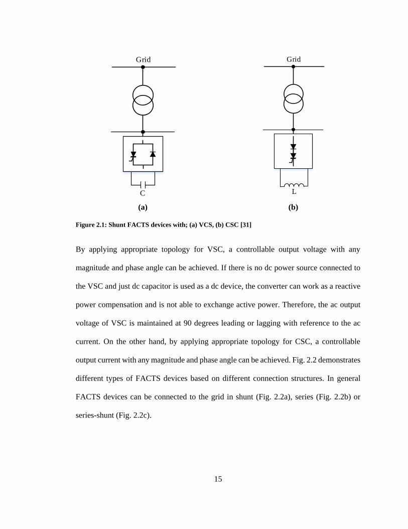
Fig. 2.1 shows the principle of VSC and CSC. As represented in Fig. 2.1a, the VSC is
comprised of dc capacitor as its voltage source connected to switching devices parallel
with the reverse diode. Fig. 2.1b shows a CSC consists of the dc reactor as its current
source connected to the switching devices series with a diode.
15
Grid
C
L
Grid
(a) (b)
Figure 2.1: Shunt FACTS devices with; (a) VCS, (b) CSC [31]
By applying appropriate topology for VSC, a controllable output voltage with any
magnitude and phase angle can be achieved. If there is no dc power source connected to
the VSC and just dc capacitor is used as a dc device, the converter can work as a reactive
power compensation and is not able to exchange active power. Therefore, the ac output
voltage of VSC is maintained at 90 degrees leading or lagging with reference to the ac
current. On the other hand, by applying appropriate topology for CSC, a controllable
output current with any magnitude and phase angle can be achieved. Fig. 2.2 demonstrates
different types of FACTS devices based on different connection structures. In general
FACTS devices can be connected to the grid in shunt (Fig. 2.2a), series (Fig. 2.2b) or
series-shunt (Fig. 2.2c).

16
Vdc
VS LS RS iL
Load
Controller
Vdc
VS LS RS
iref
iL
Vdc
Shunt FACTS
Load
iref
iL
Shunt FACTS
VSLS RS
vref
Series FACTS
Vdc
Controller
(a)
(b)
(c)
Controller
Vdc
Series FACTS
Load
vref
Figure 2.2: FACTS device connection topologies; (a) shunt, (b) series, (c) series-shunt [32]
Different connection types and switching devices of converters result into several
different operating features. Therefore, the compensation of reactive power can be divided
to the three main groups [64]. The first group is conventional mechanically switched
devices including fixed shunt reactor (FR), fixed shunt capacitor (FC), mechanical
switched shunt reactor (MSR) and mechanical switched shunt capacitor (MSC).

17
Second group is known as thyristor-based devices including force-commutated devices
such as integrated gate-commutated thyristor (IGCT), insulated gate bipolar transistor
(IGBT), gate turned-off thyristor (GTO) and MOS-controlled thyristor or self-
commutated devices which are thyristor controlled reactor (TCR), thyristor switched
capacitor or reactor (TSC/TSR), static VAR compensator (SVC), thyristor switched series
compensator capacitor or reactors (TSSC/TSSR), thyristor controlled series compensator
capacitors or reactors (TCSC/TCSR) [65], thyristor controlled braking resistors (TCBR),
thyristor controlled phase shifting transformers (TCPST), thyristor controlled phase angle
regulator (TCPR) and line commutated converter compensator (LCC).
The last group is identified as converter-based devices including StatCom, static
synchronous series compensator (SSSC) [66], unified power flow controller (UPFC) [67],
interline power flow controller (IPFC) [68] and self-commutated compensator (SCC).
Fig. 2.3 demonstrates some of these devices including TSR/TCR, TSC, TCSR/TSSR and
TCSC/TSSC.
The conventional thyristor devices have only turn-on control and their turn-off capability
depends on system conditions. Some devices such as GTO, IGBT, IGCT and other
devices have turn-on and turn-off capability. However, compared to devices without turn-
off capability, they are more expensive with higher losses. The conventional thyristor-
based converters without turn-off capability can only be used in CSCs while devices with
turn-off capability can be used in both VSCs and CSCs.

18
L
T1 T2
Transformer
Grid
C
T2
Transformer
Grid
Grid
(c)
Grid
(a) (b) (d)
Figure 2.3: FACTS device building blocks; (a) TSR/TCR, (b) TSC, (c) TCSR/TSSR, (d) TCSC/TSSC
[31]
The TCR is a shunt compensator which regulates the equivalent inductive reactance of
distribution network line by adjusting the phase angle. It consists of bidirectional thyristor
series with the reactor. The TSC is similar to TCR but using power capacitor in series
with the bidirectional thyristor. The constraint of these compensators is that they only can
perform continuous inductive or discontinuous capacitive compensation while most of the
applications need continuous inductive or capacitive compensation. Then SVC is
introduced as a device able to deliver continuous inductive and capacitive compensation.
Fig. 2.4 shows classification of FACTS devices based on four groups of series, shunt,
combined series-series and combined series-shunt converters.

19
FACTS
SeriesSeries-
Series
Series-
Shunt
SSSC TSSC TCSC
Shunt
StatComSVC IPFC UPFC
Figure 2.4: FACTS devices based on different connection topologies [31]
2.3 Control Methods of Shunt Converters for FACTS Applications
The basic shunt FACTS device control methods are studied based on PWM controls of
VSC. However, the recent advanced shunt FACTS devices are based on multilevel VSCs.
It is imperative to reduce the VSC losses to increase its efficiency. Among different losses
of VSCs, switching losses are very important and thus, proper control method should be
applied to limit the overall losses. Among different control methods, sinusoidal PWM
(SPWM), selective harmonic elimination PWM (SH-PWM), space vector PWM (SV-
PWM) and hysteresis control PWM (HYS-PWM) are strong and robust control methods
[69-72].
Some other control methods such as linear, fuzzy, sigma-delta, optimized and
proportional-resonant control methods are used in shunt FACTS devices [73-75].
2.3.1 Sinusoidal PWM (SPWM)
This method has been used extensively in shunt FACTS devices due to its easy structure
and simple mathematical requirements. Even very basic and simple microcontrollers can

20
implement this simple method. It works based on comparing a triangle carrier waveform
with a sinusoidal modulation signal to get the proper switching.
2.3.2 Space Vector PWM (SV-PWM)
This method is more suitable to be used in multilevel converters since it can produce 15
percent higher output voltage than the other control methods.
The circuit model of a three-phase voltage source PWM inverter is shown in Fig. 2.5. In
this model, S1 to S6 are the six power switches, which are controlled by the switching
variables a, a1, b, b1, c and c1. When an upper transistor is switched on (i.e., when a, b or
c is 1), the corresponding lower transistor is switched off (i.e., the corresponding a1, b1 or
c1 is 0). Therefore, the on and off states of the upper transistors S1, S3 and S5 can be used
to determine the output voltage.
The relationship between the switching variable vectors (a, b, and c) and the line-to-line
and phase voltage vectors are given by Eqs. 2.1 and 2.2, respectively:
c
b
a
dcV
caV
bcV
abV
101
110
011
(2.1)
c
b
adc
V
cnV
bnV
anV
211
121
112
3 (2.2)
There are eight possible combinations of on and off patterns for the power switches. Based
on Eqs. 2.1-2.2, the eight switching vectors, output line to neutral and line-to-line voltages
in terms of dc-link (Vdc), are given in Table 2.1.

21
Va
Vb
Vc
Vdc
a b c
a1 b1 c1
S1 S3 S5
S4 S6 S2
Vn
LS-a RS-a
LS-b
LS-c
RS-b
RS-c
iL-a
iL-b
iL-c
Load
Figure 2.5: Three-phase voltage source PWM inverter [33]
According to Table 2.1, the six nonzero vectors (V1-V6) shape the axes of a hexagonal
(Fig. 2.6) and feed electric power to the load.
Table 2.1: Eight inverter voltage vectors (V0-V7)
Voltage
vectors
Switching
Vectors
Line to Neutral
Voltage
Line to Line
Voltage
a b c Van Vbn Vcn Vab Vbc Vca
V0 0 0 0 0 0 0 0 0 0
V1 1 0 0 2/3 -1/3 -1/3 1 0 -1
V2 1 1 0 1/3 1/3 -2/3 0 1 -1
V3 0 1 0 -1/3 2/3 -1/3 -1 1 0
V4 0 1 1 -2/3 1/3 1/3 -1 0 1
V5 0 0 1 -1/3 -1/3 2/3 0 -1 1
V6 1 0 1 1/3 -2/3 1/3 1 -1 0
V7 1 1 1 0 0 0 0 0 0

22
Figure 2.6: The basic switching vectors and sectors [33]
The angle between any adjacent two non-zero vectors is 60 degrees. Meanwhile, the two
zero vectors (V0 and V7) apply zero voltage to the load. The objective of space vector
PWM technique is to approximate the reference voltage vector Vref using the eight
switching patterns [76].
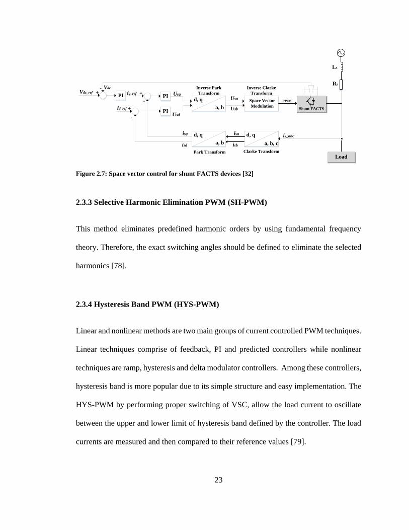
Fig. 2.7 shows a sample of SV-PWM control for StatCom application. The switching
signals of SV-PWM modulator is produced by using the switching vector in complex
space of (d, q). The three-phase voltage vectors are generated by power source pass α-β
and d-q transformer blocks to be converted to two phase vectors. Then d-axis current and
q-axis current are compared with their related reference currents. Then the error passes
through PI controller and finally the SV-PWM generates the switching signals of the
StatCom. Moreover, the Clark transformation is converting the three phase load currents
to d-axis for controlling the dc voltage of the device and q-axis for controlling the reactive
power of the network [77].
23
+
-+
PI + PI
+ PI
Space Vector
Modulation
d, q
a, b
d, q
+
-
+
-
d, q
a, b
Load
Shunt FACTS
a, b, c
Inverse Clarke
Transform
Inverse Park
Transform
Park Transform Clarke Transform
PWMUsa
Usb
isq
isb isd
isa
Vdc
Vdc_ref
id_ref
Usq
Usd
iq_ref
is_abc
LS
RS
Figure 2.7: Space vector control for shunt FACTS devices [32]
2.3.3 Selective Harmonic Elimination PWM (SH-PWM)
This method eliminates predefined harmonic orders by using fundamental frequency
theory. Therefore, the exact switching angles should be defined to eliminate the selected
harmonics [78].
2.3.4 Hysteresis Band PWM (HYS-PWM)
Linear and nonlinear methods are two main groups of current controlled PWM techniques.
Linear techniques comprise of feedback, PI and predicted controllers while nonlinear
techniques are ramp, hysteresis and delta modulator controllers. Among these controllers,
hysteresis band is more popular due to its simple structure and easy implementation. The
HYS-PWM by performing proper switching of VSC, allow the load current to oscillate
between the upper and lower limit of hysteresis band defined by the controller. The load
currents are measured and then compared to their reference values [79].

24
2.4 Multilevel Power Converters
By growing the power system and increasing the power demand, many customers began
to use electrical loads with higher power devices. Meanwhile, there are a big number of
loads operating at medium voltages with medium power demands of megawatt power
levels. For this level of voltage and power, it is very hard to use only one semiconductor
switch for power quality purposes. Thus, multilevel converters were introduced to
overcome these problems and to be used in medium voltage high power conditions.
Moreover, another advantage of multilevel converters is using renewable energies such
as wind, PV and fuel cells as an energy sources or interface between them [80-82]. The
first three-level converter was introduced 1975 and then several topologies were
developed [83-92]. The basic concept of multilevel converters is to use several
semiconductor switches in series to achieve higher power ratings. Also, the dc source
elements (capacitors, batteries or renewable energy voltage sources) are connected in
series and the communication of power switches, combine these dc sources to reach high
voltage levels at the output.
The most important benefits of multilevel converters over the conventional two-level
converters are: i) staircase output voltage which not only results to have low distorted
output voltage, also reduces the dv/dt stresses and consequently lower electromagnetic
compatibility problems, ii) higher power outputs, iii) they draw input currents with low
distortion, and iiii) they can operate at both high switching frequencies or fundamental
switching frequencies.
25
However, multilevel converters have some disadvantages such as using a higher number
of semiconductor switches which make their control topology to be more complicated and
the overall system to be more expensive.
Many multilevel converter topologies are proposed by different researchers. Among them,
three main multilevel converter structure are defined including diode clamped, cascaded
H-bridge and flying capacitor multilevel converters. Moreover, many modulation
techniques and control strategies are introduced such as SH-PWM, SPWM, SV-PWM,
HYS-PWM. The multilevel converters can be used in several applications such as
electrical medium voltage motors [82] [93], FACTS devices [94], interface for renewable
energy systems [95] and traction drive systems [96]. Multilevel converters also have been
used as variable speed drives and static SVCs [97-107].
2.4.1 Multilevel Power Converter Structures
The three multilevel converter structures including diode clamped, flying capacitor and
cascaded H-bridge multilevel converters are described in this section.
2.4.1.1 Diode-Clamped Multilevel Converter
The first diode-clamped multilevel converter (DCMC) was introduced first by [84] in
1981 with three level diode clamped converter topology. Later on the 1990s, more DCMC
topologies of four, five and six level diode-clamped converters have been developed. The
DCMC uses capacitors in series to divide up the dc bus voltage into a set of voltage levels.
To generate m-level phase voltage waveform, a DCMC needs m-1 capacitors on the dc

26
bus. A three-phase, five-level DCMC is shown in Fig. 2.8. The dc bus consists of four
capacitors: C1, C2, C3 and C4. For a dc bus voltage Vdc, the voltage across each capacitor
is Vdc/4, and each device voltage stress will be limited to one capacitor voltage level,
Vdc/4, through clamping diodes.
Table 2.2 represents the output voltage levels possible for phase A of this inverter. State
condition 1 means the switch is on, and 0 means the switch is off. Each phase has four
complementary switch pairs such that turning on one of the switches of the pair requires
that the other complementary switch is turned off. The complementary switch pairs for
phase leg A are (Sa1
, Sa’1
), (Sa2
, Sa’2
), (Sa3
, Sa’3
), and (Sa4
, Sa’4
). Table 2.2 also shows
that for a five-level inverter, a set of four switches is on at any given time.
Figure 2.8: Three-phase five-level DCMC [80]
C1
C2
C3
C4
Sa1
Sa2
Sa3
Sa4
Sa`1
Sa`2
Sa`3
Sa`4
.
.
.
Sb1
Sb2
Sb3
Sb4
Sb`1
Sb`2
Sb`3
Sb`4
.
.
.
Sc1
Sc2
Sc3
Sc4
Sc`1
Sc`2
Sc`3
Sc`4
.
.
.
...a b co.Vdc
+
-

27
DCMCs have some advantages such as high efficiency for fundamental frequency
switching, minimization of capacitance requirements of the converter due to share a
common dc bus among all phases. Therefore, back to back topology can be used in this
converter and is suitable for high voltage converters and speed drives. However, these
multilevel converters have some disadvantages. One of them is the number of clamping
diodes which are quadratic of the level numbers which can be increased dramatically with
increasing the number of levels [80].
Table 2.2: Five-level inverter voltage levels of DCMC with corresponding switch states
VAO Switch State
Sa1 Sa2 Sa3 Sa4 Sa´1 Sa´2 Sa´3 Sa´4
V1 = 0 0 0 0 0 1 1 1 1
V2 = Vdc/4 0 0 0 1 1 1 1 0
V3 = Vdc/2 0 0 1 1 1 1 0 0
V4 = 3Vdc/4 0 1 1 1 1 0 0 0
V5 = Vdc 1 1 1 1 0 0 0 0
2.4.1.2 Flying Capacitor Multilevel Converter
This multilevel converter was introduced by [108] in 1992. The structure of flying
capacitor multilevel converter (FCMC) is similar to DCMC except that this converter uses
capacitors instead of diodes. Fig. 2.9 shows the structure of FCMC. As can be seen, this
topology has a ladder structure of dc capacitors for which the voltage on each capacitor
differs from that on the next capacitor. To produce m-level staircase output voltage, m-1
capacitors in the dc bus are needed. Each phase leg has an identical structure. The size of
the voltage rise between two capacitors determines the size of the voltage levels in the
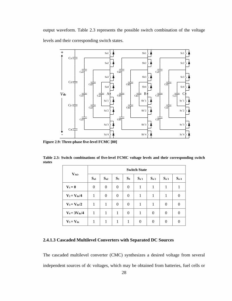
28
output waveform. Table 2.3 represents the possible switch combination of the voltage
levels and their corresponding switch states.
Figure 2.9: Three-phase five-level FCMC [80]
Table 2.3: Switch combinations of five-level FCMC voltage levels and their corresponding switch
states
VAO
Switch State
Sa1 Sa2 S3 S4 Sa´1 Sa´2 Sa´3 Sa´4
V1 = 0 0 0 0 0 1 1 1 1
V2 = Vdc/4 1 0 0 0 1 1 1 0
V3 = Vdc/2 1 1 0 0 1 1 0 0
V4 = 3Vdc/4 1 1 1 0 1 0 0 0
V5 = Vdc 1 1 1 1 0 0 0 0
2.4.1.3 Cascaded Multilevel Converters with Separated DC Sources
The cascaded multilevel converter (CMC) synthesizes a desired voltage from several
independent sources of dc voltages, which may be obtained from batteries, fuel cells or
C1
C2
C3
C4
Vdc
+
-
Sa1
Sa2
Sa3
Sa4
Sa`1
Sa`2
Sa`3
Sa`4
.ACa1
Ca2
Ca2
Ca3
Ca3
Ca3
Sb1
Sb2
Sb3
Sb4
Sb`1
Sb`2
Sb`3
Sb`4
.BCb1
Cb2
Cb2
Cb3
Cb3
Cb3
Sc1
Sc2
Sc3
Sc4
Sc`1
Sc`2
Sc`3
Sc`4
.CCc1
Cc2
Cc2
Cc3
Cc3
Cc3

29
solar cells. This new converter can avoid extra clamping diodes or voltage-balancing
capacitors. The number of output phase voltage levels is defined by m= 2N+1, where N
is the number of DC sources.
Figure 2.10: Three-phase (2N+1)-level CMC [80]
A three-phase structure of an m-level cascaded inverter is illustrated in Fig. 2.10. Each dc
source is connected to separated inverter to produce three output voltages of +Vdc, 0 and
–Vdc. This can be achieved by a different combination of switches S1, S2, S3 and S4. If
switches S1 and S4 are turned on, +Vdc is generated while this value is –Vdc if switches
S2 and S3 are turned on. Also, the output voltage is zero when switches S1 and S2 or S3
and S4 are turned on. Moreover, the output voltages of all inverters are connected in series
in each phase to produce the synthesized voltage waveform of the sum of the inverter
outputs.
CMCs can be used for interface with renewable energy sources, static VAR generation
and battery based applications. They are ideal for connecting renewable energy sources

30
to an AC power networks because they need separated dc energy sources such as PV or
fuel cells. Traction drive is another application of CMCs which is used in electric vehicles
[103].
CMCs have some advantages over other multilevel converters. The number of output
levels is more than the twice number of dc sources and due to the modularity of converters
in CMCs, it is easier and quicker to process and manufacture them. The drawback of this
converters is a requirement of dc sources for each module [106].
Some other researchers have proposed a different CMC topology which including the
different value of dc levels instead of equal values (usually dc sources are multiple of each
other) [104-105]. Moreover, they use a combination of two switching topologies of PWM
switching and fundamental frequency switching. This topology enables the CMCs to have
more output level comparing to the conventional CMCs.
2.4.2 Comparison among Multilevel Converters
According to the standards, the reliability of the system is proportional to the number of
its components. For comparing different multilevel converters, the clamping diodes are
used only in DCMC and are not required in the FCMC and CMC, while balancing
capacitors are only used in FCMC. Based on Fig. 2.11, CMCs required the minimum
number of total main components. However, they need more capacitors compared to
DCMCs, but this is not considered as a disadvantage. Circuit layout flexibility is one of
the advantages of using CMCs. This fact makes CMCs be more popular and easier to be
built. Each level in CMCs has the same structure and also there are no extra voltage-
balancing capacitors or clamping diodes which are required in FCMC and DCMC. To

31
achieve a higher number of output levels, only adding more numbers of modules is
needed.
To achieve high voltage levels in FCMCs, an undesirable amount of capacitors is required.
For an instance, in CMCs only three capacitors are required to get seven level output while
this number is 15 in FCMCs plus six dc link capacitors.
Table 2.4 compares the power component requirements per phase leg among three
multilevel converters of DCMC, FCMC and CMC.
150
100
50
05 73 9 11
Number of phase voltage levels
Nu
mb
er o
f to
tal
com
po
nen
ts
CMC
FCMC
DCMC
Figure 2.11: Number of components required in the multilevel converters as a function of the number
of voltage levels [80]
Table 2.4: Comparison of power component requirements per phase leg among three multilevel
converters
Converter Configuration DCMC FCMC CMC
Main Switching Devices 2(n-1) 2(n-1) 2(n-1)
Main Diodes 2(n-1) 2(n-1) 2(n-1)
Clamping Diodes (n-1)(n-2) 0 0
DC Bus Capacitors n-1 n-1 (n-1)/2
Balancing Capacitors 0 (n-1)(n-2)/2 0
Total Components n2+2n-3 (n2+8n-8)/2 (9/2)(n-1)

32
2.4.3 Asymmetric Multilevel Converters
The asymmetric hybrid multilevel converters synthesize the output voltage waveforms
with lower harmonic contents compared to other multilevel converters. This advantage is
achieved by using distinct voltage levels in different modules, which can generate more
levels in output voltage waveform and reduces the THD ratio while preventing to increase
the number of switching devices and sources. Usually, multilevel converters use equal dc
voltage value for each cell. However, it is possible to increase the maximum number of
output voltage levels by using different dc voltage values. Therefore, asymmetric
multilevel converters can provide a higher number of output voltage levels compared to
symmetric multilevel converters [109-111]. Consequently, due to lower THD of the
output voltage, the filtering devices can be removed or can be selected optimally small
and efficient and therefore, the converter efficiency is increased. The relationship among
the dc-link voltages to provide a regularly stepped output voltage waveform could be
binary (power of two) or trinary (power of three). The maximum numbers of output
voltage levels are given by:
12 )1( NbinaryasymmetricL (2.3)
NtrinaryasymmetricL 3 (2.4)
Fig. 2.12 demonstrates a three-phase asymmetric multilevel converter. In these
converters, if the ratio step of dc sources is binary then the output voltage levels of the
converter are 15 levels (Eq. 2.3), while if this ratio is trinary, then 27 level output voltage
is generated (Eq. 2.4). In these multilevel converters, it is possible to use high switching

33
frequency for one cell while the other cells can use low switching frequency. Therefore,
the main cell can use IGBT while the rest use GTO as their switching devices [112].
Figure 2.12: Three-phase asymmetric multilevel converter [109]
The switching of multilevel converters is divided to fundamental switching frequency and
high switching frequency PWM. Fig. 2.13 illustrates different types of control techniques
for multilevel converters.
Multilevel Converters
Control Techniques
High Switching
FrequencyPWM Fundamental
Switching Frequency
Space Vector ControlSelective Harmonic
Elimination Sinusoidal PWMSpace Vector PWM
Figure 2.13: Different control techniques for multilevel converters [69]

34
2.5 StatCom
Power utilities are facing many challenges due to increasing complexity in the operation
and structure of distribution systems as well as the growing appetite to increase the
penetration of renewable energy resources. Voltage instability issues such as voltage sag
and swell are among the main problems that power utilizes are facing [113-114]. Voltage
sag and swell are the two most common issues contributing to the power quality problems
in power systems [15]. The consequences of voltage sag can lead to partial or full power
interruption in the system. The well-known solution to protect the network from voltage
quality and voltage collapse problems is to inject or absorb reactive power to or from the
network. High penetration of PV power generation has brought significant technical
challenges to the distribution systems such as voltage rise, protection coordination and
harmonic distortions. Among these problems, over-voltage caused by reverse power flow
has become a significant issue for power systems [115]. There are a few solutions to
overcome this issue such as changing the transformer ratio to have lower secondary
voltage [20] or decrease the line impedances by changing conductor sizes [21]. However,
these methods are not able to cover all problems. In addition, the voltage instability has
harmful effects on most electronics devices. For example, modern industrial equipment
are based on electronic devices which are very sensitive to disturbances [56] such as
voltage sags, voltage swells and harmonics. Various methods have been proposed to
improve the voltage instability.
The main approach is to compensate the reactive power. Capacitor banks were one of the
first methods for reactive power control. They can be used to control the reactive power
and improve the power factor by injecting the necessary reactive power of a connected
35
point and thus reduce the flow of reactive power in related lines which consequently
improve the voltage profile of connected points. The amount of generated reactive power
by capacitor bank is:
2
CC CVQ (2.5)
where is the angular frequency of the network, C represents the capacitance of the
module and Vc is the amplitude voltage of the connected bus.
The VSC-based StatCom is gained more attention among other converters due to its high-
quality technology compared to thyristor-based SVC and is used as a dynamic shunt
compensator. On the other hand, GTO-based VSCs and also IGBTs and IGCTs are used
in high power rating controllers. However, their implementation is mainly still in low to
medium rating controllers due to some limitations.
The conventional compensation of reactive power such as shunt capacitor or inductor
banks has many disadvantages such as fixed compensation, resonance, large size and
weight, as well as noise and losses. However, these are not ultimate solutions due to
uncontrollable reactive power compensation and high costs of installing new feeders.
Recent approaches include the application of StatCom have proven their effectiveness not
only for voltage instability correction but also for other power quality issues such as
flicker suppression, power factor correction and harmonic control [116-118]. The main
features of StatCom are quick response time, exceptional dynamic characteristics under
various operating conditions, less space requirement and more flexible in operation.
StatCom is a reactive power compensation device that is shunt connected to the AC
distributions systems. It is defined as a self-commutated switching converter with the
energy source (usually capacitor) connected to the power network injects or absorbs

36
reactive current through the power network to regulate the amount of reactive power of
the connected point by exchange reactive power between the converter and connected
network. In general, when two ac power sources of the same frequency are connected to
each other, the active power flows from leading to lagging source. As a result, in StatCom
the voltage angle of converter is tuned to be the same as the connected network to prevent
active power exchange between two sources. However, in practice there is a small angle
shift between two sources in order to compensate the losses of the converter. The reactive
power flow is specified by the voltage magnitude difference between the converter and
network. Therefore in StatCom, the reactive power flow can be controlled by changing
the fundamental component of converter voltage. The StatCom is located between
generators and loads. These principles make StatCom act as a source or either a load in
power networks.
The more recent approach to improve the voltage profile is based on the application of
distribution StatCom (D-StatCom) with the additional capability of sustaining reactive
current at low voltage levels that can be utilized for both voltage and frequency support
by replacing capacitor banks with batteries as the energy storage devices [119]. D-
StatCom injects a compensation current into the system to correct the power quality
disturbances such as voltage sag and swell. Its applications are mainly for protecting
sensitive loads that may be significantly affected by oscillations in the system voltage and
current [120-121].
As mentioned before, StatComs are considered as a FACTS family members who can
replace SVCs in distribution networks. The StatCom is capable of improving the power
quality of the distribution networks by performing several compensations such as voltage

37
flicker, sag and swell control, dynamic voltage control, damping the oscillations of power
lines, and active and reactive power control of distribution networks. These achievements
are reachable since StatCom uses voltage source converters, developed control methods
and on-off switches.
As mentioned, StatComs mostly use VSC converters in most of their applications. These
converters comprise of self-commutating solid-state turn-off switches such as IGBT,
GTO and so on with a reverse diode connected in parallel to them. These switches can
work with a different mode of operations including PWM mode with high switching
frequencies in a cycle or square-wave mode with once per cycle or selective harmonic
elimination with low switching frequencies. StatCom in general consists of six pulse
VSC-converter, a dc bus connected to dc energy storage device, a controller and a
coupling transformer interfacing the converter output and connected system voltage. The
relation of active and reactive power injected by StatCom at the PCC is based on Eq. 2.6.
L
S
L
CS
L
CS
X
V
X
VVj
X
VVjQPS
2
cos3sin3 (2.6)
where S is the apparent power, P active power, Q reactive power, SV phase voltage of
connected bus, CV fundamental output phase voltage of StatCom,
LX leakage reactance (
fLX L 2 , f system frequency) and the phase angle between SV and
CV .
As can be seen from Eq. 2.6, if the phase angle of StatCom output voltage is controlled to
be same as the network voltage angle, will be zero and consequently there will be no
active power exchange between two sources. Thus, the exchange of active power depends
on the amount of . In Eq. 2.6, if equals to zero then Eq.2.7 is resulted:

38
SC
L
S VVX
VQ 3 (2.7)
To achieve optimal reactive power control, StatCom injects a current in quadrature with
the network voltage (SV ) lagging or leading and react as an active or reactive load for the
network. The magnitude and phase angle of injected current of StatCom are determined
by the magnitudes of SV ,
CV and the phase difference between them ( ). When the
converter voltage (CV ) is bigger than network voltage (
SV ), the StatCom injects reactive
power to the network and StatCom operates in a capacitive mode; and when SV is greater
thanCV , the StatCom operates in inductive mode and absorbs reactive power from the
connected network. For no reactive power exchange between StatCom and network, the
magnitude of two sources is the same (SV =
CV ).
2.5.1 Comparison of SVC and StatCom
StatCom has some benefits over SVC such as smaller size due to the elimination of
capacitor banks and reactors and faster response. Also, StatCom can be considered as a
controllable current source beyond the limitation of bus voltage. Moreover, due to high
dependency of SVC on the supply voltage (Eq. 2.5), its reactive power compensation is
decreased with a decrease in supply voltage, while the StatCom can supply required
reactive power even at low supply voltage. This feature of StatCom especially improves
the transient stability of the system. On the other hand, the SVC is cheaper than StatCom
and is a better choice for applications which need very high reactive power compensation
due to its lower losses [31].

39
Fig. 2.14 shows an equivalent circuit of StatCom including dc source (capacitor),
converter and filter. The filter consists of a resistance Rs and inductance Ls. The main
objective of VSC is to produce almost pure sinusoidal AC voltage with the minimum of
harmonic distortions from a dc voltage source. In Fig. 2.14 the series inductance (Ls)
represents the leakage of the transformer and the resistance (Rs) signifies the active losses
of the transformer and converter.
Figure 2.14: Equivalent circuit diagram of StatCom [33]
2.6 Harmonics as a Power Quality Problem
By developing the power electronic technology, the use of nonlinear loads in commercial,
industrial and residential installations such as rectifiers, converters, adjustable speed
drives, arc furnaces and computer power supplies is growing rapidly. As a result, the
harmonic levels in power distribution networks are increased. These loads inject the
harmonic currents into the system and distort the voltage waveforms. This distortion
causes various unwanted effects for the linear loads connected at the same PCC.
Harmonics were detected first around the 1920s [2]. Harmonic content (distortion), in the

40
system are measured based on the ratio of the amplitude of each harmonic to the amplitude
of the fundamental component of the supply system voltage or current.
According to IEEE Standard 519-1992 [38], the maximum allowable THDv for
distribution lines, i.e. 69 kV and below, is 5% and for each individual harmonic voltage
is limited to 3%. The current harmonic limits differ based on the short circuit strength of
the system. Basically, if the system is able to handle more harmonic currents, customers
also are allowed to inject more harmonic currents. Tables 2.5 and 2.6 show the IEEE
Standard 519-1992 for harmonic voltage and harmonic current, respectively.
2.6.1 Harmonic Sources
Generally, there are three main groups of harmonic sources including i) saturable devices,
such as transformers, ii) arcing devices, such as arc welders and arc furnaces and iii)
power electronic devices such as variable speed drives, battery chargers and most of
rectifier and inverter applications.
2.6.2 Effects of Harmonics
Harmonics in power systems can have injurious impacts on the network operation and its
components, such as overheating of power transformers, motors and cables; creating
harmonic resonances; causing low power factor conditions and mal-operations of
protection devices [37]. Therefore, it is essential to compensate these distortions to
minimize their effects on the system and to increase the system efficiency.

41
Table 2.5: Harmonic voltage limits (IEEE Std. 519-1992) [38]
Bus voltage V at PCC Individual harmonic
distortion (%)
Total harmonic
distortion THD (%)
V≤ 1.0 kV 5.0 8.0
1.0 kV≤ V ≤ 69 kV 3.0 5.0
69 kV ≤ V ≤ 161 kV 1.5 2.5
161 kV ≤ V 1.0 1.5*
* High-voltage systems can have up to 2.0% THD where the cause is an HVDC terminal
whose effects will Have attenuated at points in the network where future users may be
connected.
Table 2.6: Harmonic current limits for general distribution systems (IEEE Std. 519-1992) [38]
Maximum Harmonic Current Distortion in Percent of IL
Individual Harmonic Order (Odd Harmonics)
Isc/IL h<11 11≤h<17 17≤h<23 23≤h<35 35≤h TDD
<20* 4.0 2.0 1.5 0.6 0.3 5.0
20<50 7.0 3.5 2.5 1.0 0.5 8.0
50<100 10.0 4.5 4.0 1.5 0.7 12.0
100<1000 12.0 5.5 5.0 2.0 1.0 15.0
>1000 15.0 7.0 6.0 2.5 1.4 20.0
Even harmonics are limited to 25% of the odd harmonic limits above.
Current distortions that result in a dc offset, e.g. half-wave converters, are not allowed.
* All power generation equipment is limited to these values of current distortion, regardless of actual
Isc/IL.
Where
Isc = maximum short-circuit current at PCC.
IL = maximum demand load current (fundamental frequency component) at PCC.
TDD = Total demand distortion (RSS), harmonic current distortion in % of maximum demand load current (15 or 30
min demand).
2.7 Harmonic Mitigation Techniques
To eliminate the harmonics from the network, filtering devices are needed. There are
different filter topologies presented in the literature for this purpose.

42
Basically, there are two approaches of compensating harmonic distortions including
passive filters and active filters.
2.7.1 Passive Harmonic Filters
The Passive filters are mainly made of resistive, capacitive and inductive components.
They usually eliminate harmonics by tuning the component to generate resonance at the
selected harmonic frequency. They are connected in series or shunt with the power
system. Series passive filters designed to have large impedances at selected harmonics to
isolate the produced load harmonics from the power source. On the other hand, shunt
passive filters designed to have a low impedance for selected harmonics to allow those
harmonics pass through the filter to the ground. Although passive filters are relatively
cheaper than other filters, they have some disadvantages preventing using them widely.
Passive filters are designed to filter specific harmonic components and can not be applied
for the elimination of large variation of harmonic components. Moreover, passive filters
usually have big sizes and for applications with higher voltages can not be used. It is
noticed in some cases; it is very hard to tune the filters due to interacting of other
harmonics drawn from other power sources. Resonance is another drawback of these
filters. Additionally, the capacitance component of passive filters can interact with the
system impedance and result in resonance conditions and in some cases can increase the
harmonic rates of power system results in a very bad voltage profile.

43
2.7.2 Active Filters
To overcome the drawbacks of passive filters, active compensation is introduced. APFs
were introduced around 1970. The active power filtering devices can be connected in
series (DVR), shunt (APF), or series-shunt configuration (UPQC) [122-133]. Generally,
they use VSC as a controller while some other use CSC which is not popular. Also, they
are divided into different classifications of single phase (two-wire) or three-phase (three-
wire or four-wire) systems.
The VSC is more popular because it can be used in multilevel and multi-step converters
to increase the power capacity of converter and be able to work with lower switching
frequencies. Moreover, the dc capacitor in VSC can be replaced with energy storage
devices to exchange active power with the network [134].
APF injects harmonic current equal but opposite to the harmonic current produced by the
nonlinear load. It acts as a current source injecting harmonics. Fig. 2.15 shows the three-
phase line diagram of APF with the corresponding waveforms.
Electrical
Power Grid
Controller Inverter
Nonlinear
Load 1
Isa
Isb
Isc
Va
Vb
Vc
ILa
ILb
ILc
Ica
Icb*
Icc*
Icb
Icc
ILa
ILb
ILc
= +
Ica*
Vdc
+ -
Is Ic IL
..
.
..
.
..
.
(a)

44
APF
APF APF
(b)
Figure 2.15: APF; (a) three-phase circuit diagram, (b) voltage and current waveforms before and
after connection of APF
Fig. 2.16 shows the DVR connected in series with the network including matching
transformer capable of eliminating voltage harmonics and regulate and balance the
voltage of connected bus. It injects voltage components in series with the main voltage
and consequently, compensating voltage sag and swell on the load side. Also, the
harmonic voltages are added to maintain almost pure sinusoidal voltage across the load.
VC
VS LS RS iL
DVR
LoadiS
Figure 2.16: DVR circuit diagram [124]

45
Fig. 2.17 shows a three-phase three-wire UPQC comprises of shunt and series converters.
There is a shared dc bus between two converters able to work as an active series and active
shunt compensator. UPQC is considered as the most useful custom power devices capable
of regulate and balance the voltage, compensating the reactive power and improving the
power quality. However, its high installation costs and control complexity prevent it to be
the only solution to the power quality. In general, UPQC has two topologies of right-shunt
[127] and left-shunt [128].
Figure 2.17: Three-phase three wire UPQC [128]
According to standards, consumers are responsible to keep their injected harmonic current
magnitudes and THDi at their PCCs below the permissible levels while utilities are
required to control the THDv of the network and the individual buses [37-38]. Therefore,
each nonlinear load which exceeds the standard level must install APF at their connection
point to eliminate their undesired harmonic current. However, by installing APF at each
nonlinear load bus, the THD of related bus reduces to zero. This is because APF injects
exactly the same amount of harmonic current produced by nonlinear load and hence,
eliminates all harmonic currents of the nonlinear load. Fig. 2.18 shows how APF is
connected to each nonlinear load in the network.
Vdc
LS-b RS-b
LS-c RS-c
LS-a RS-a
Nonlinear
Load

46
Nonlinear
Load 1
Isabc
linear
Load 2
IAPF
Reference
Current
Generator
Iref.abc*Converter
Vsabc
ILabc
APF APF APF
Electrical
Power
Grid linear
Load 1
Nonlinear
Load 2
Nonlinear
Load Nlinear
Load 3
linear
Load N
Figure 2.18: Single line diagram of APF connected to the distribution network
2.7.3 Harmonic Current Extraction Techniques
There are two fundamental approaches to extract harmonic currents in APFs applications
which are a correction in time-domain and correction in frequency-domain [39] [132].
Fig. 2.19 represents different types of harmonic extraction techniques. The advantage of
time-domain methods is the fast response for online applications without complicated
control circuitry. This advantage occurs because time-domain control strategies operate
on instantaneous values of the distorted waveform, rather than on at least one period, as
in frequency-domain methods so that the required computational time can be relatively
small. The shortcoming of time-domain methods is that, to obtain optimum results,
relatively high switching frequencies are needed, which subsequently leads to excessive
switching losses in the semiconductor switches. On the other hand, switching frequencies
for frequency-domain methods can be much lower than in time-domain schemes, resulting
in much lower semiconductor switching losses. Their main disadvantage is longer
computational time than in the time-domain methods.

47
Frequency Based Time Based
Harmonic Current
Extraction Techniques
Kalman
Filter
Wavelet
Transform
Fast Fourier
Transform
Discrete Fourier
Transform
Fourier
Series
Sinusoidal
Tracking
Adaptive
Notch Filter
Neural
Network
Synchronous
Reference Frame
p-q-r
Theory
Cross Vector
Theoryp-q Theory
Figure 2.19: Harmonic extraction techniques [132]
2.7.4 APLC
As mentioned before, the principle concept of active filtering of harmonics was proposed
in the 1970s. They are based on completely eliminate the harmonics of nonlinear loads.
The general approach for harmonic compensation is to put regulations to force consumers
with nonlinear loads to reduce their harmonic injections to the network or install filters.
However, these methods compensate the harmonic injection of the nonlinear load at PCC
without considering the entire network [37]. APLC is capable of compensating harmonics
of the entire network to meet the network power quality requirements based on IEEE
standard 519-1992 [38]. To achieve the entire network harmonic compensation, optimal
siting and sizing of APLCs need to be considered. In general, APLCs are improved
version of APFs with some differences [40-51]. They are installed only in optimal buses
determined by optimal setting (Fig. 2.20), they control the THDv and individual voltage
harmonics of the entire network within the limits and they inject reference currents not to
fully compensate the nonlinear load distortions but just to limit the harmonic distortions
within the limits.

48
Nonlinear
Load 1
APLC 1 APLC 2
Isabc
IAPLC
Reference
Current
Generator
Iref.abc*
𝑉𝑁𝐻
𝑉1𝐻
𝑉2𝐻
Vsabc Isabc
From
Smart
Meters
Converter
Nonlinear
Load 2
Electrical
Power
Grid linear
Load 1
linear
Load 2
linear
Load 3
linear
Load N
Nonlinear
Load N
Figure 2.20: Single line diagram of APLC connected to distribution system
While there are many publications on APFs, the research on APLCs has been very limited
[40-51] mainly due to the unavailability of online network data. However, this problem
has been recently resolved with widespread installation of smart meters in SGs with
sophisticated communication networks. The research on APLCs can be classified into
optimal siting and sizing of single [40-46] and multiple [47-51] APLC units. However,
all publications on APLC siting and sizing ignore the impacts of harmonic couplings
imposed by the nonlinear devices.
Fig. 2.21 shows three-phase modular APLC with voltage source inverter connected to the
grid. The VSC consists of six power transistors with dc link capacitor which is connected
to the PCC through the inductor. The interface inductor acts here as a filtering device and
suppressing the higher order harmonic components caused by the switching operation of
the power transistors. The VSC generates current harmonics to reduce the harmonic
distortion effects of nonlinear loads, and hence bring the total THDv of the network within
the standard value.

49
Ica Icb Icc
via vib vicvca1
C C
C
C
CC
vca2
vcb1
vcb2
vcc1
vcc2
LcLc Lc
Rc Rc Rc
..
.. . .
.... . .
..
.. .
.
Figure 2.21: Three-phase asymmetric CMC APLC connected to the grid [109]

50
CHAPTER 3: REACTIVE POWER COMPENSATION USING
STATCOM
3.1 StatCom as a Shunt Connected FACTS Device
As mentioned in chapter 2, recently there has been substantial interest in reactive power
as one of the several supplementary services required for the reliability of the power
systems due to its vital effect on power system security. Solid state power conversion
devices are extensively engaged to control a wide range of electrical active and passive
loads such as variable speed drives, uninterrupted power supply (UPS) and electric
furnaces. These nonlinear loads draw harmonic currents and reactive power as well as
active power from the main AC sources. Reactive power is relative to bus voltage levels
and deficiency of enough reactive power supply leading to poor voltage profiles with the
possibility of voltage collapse within power systems. Moreover, reactive power and
harmonic components of load current reduce the system power factor leading to an
increase in transmission network losses, overheating of devices and end-user voltage
fluctuations. Furthermore, quick variations in reactive power consumption of large loads
can lead to voltage oscillations which might cause power fluctuations within the network
[13-14]. Voltage sag is defined as RMS reduction of AC voltage at the fundamental
frequency for the duration of a half-cycle to a few seconds [16]. Voltage swell is another
kind of voltage instability which may happen under different scenarios. High penetration
of PV cells is one of the main reasons for voltage rise in the system due to reversed power
flow to the network [17-18]. The conventional compensation of reactive power is based

51
on connecting shunt capacitor or inductor banks to the system through mechanical
switches. However, these methods have many disadvantages such as fixed compensation,
resonance, large size and weight, as well as noise and losses. By controlling the reactive
power within transmission and distribution networks, maximum active power flow and
voltage regulation can be achieved. The StatCom is a shunt connected FACTS device
capable of generating or absorbing reactive power and can be controlled independently of
the AC power system.
This section investigates and improves the voltage stability of distribution system
consisting of local loads and rooftop PVs. This will be done by modeling and
implementation of StatCom based on hysteresis current control (HCC). Simulations are
performed and studied in Matlab/Simulink to explore the performance and ability of
StatCom in compensating voltage quality issues.
3.1.1 The Principle of StatCom
The StatCom can be described as a voltage source converter with an energy storage unit
which is usually a dc capacitor connected to the network through a transformer. The main
objective of StatCom is to control reactive current by injecting or absorbing specified
reactive power through the connected network. Usually, StatCom output voltage is set to
be in phase with the system voltage with a small phase difference to compensate the losses
of the converter. Consequently, there would be only reactive power exchange with no real
power exchange between the StatCom and the power system [59] [135].
A single-line diagram of a StatCom power circuit is shown in Fig. 3.1a. The exchange of
the reactive power between the converter and the power system is controlled by changing

52
the amplitude of output voltage (Es) of the converter, as exemplified in Fig. 3.1b. If the
output voltage of the StatCom increases above the voltage of connected bus (Et), then the
current is injected from the converter to the power system and the StatCom provides
capacitive power to the power system. On the other hand, if the output voltage of the
StatCom decreases below the voltage of connected bus, then the current flows from the
power system to the converter and the StatCom consumes inductive power from the
network.
(a) (b)
Figure 3.1 : StatCom principle diagram; (a) power circuit, (b) reactive power exchange [34]
Fig. 3.2 shows an equivalent circuit of StatCom including dc source (capacitor), converter
and filter.
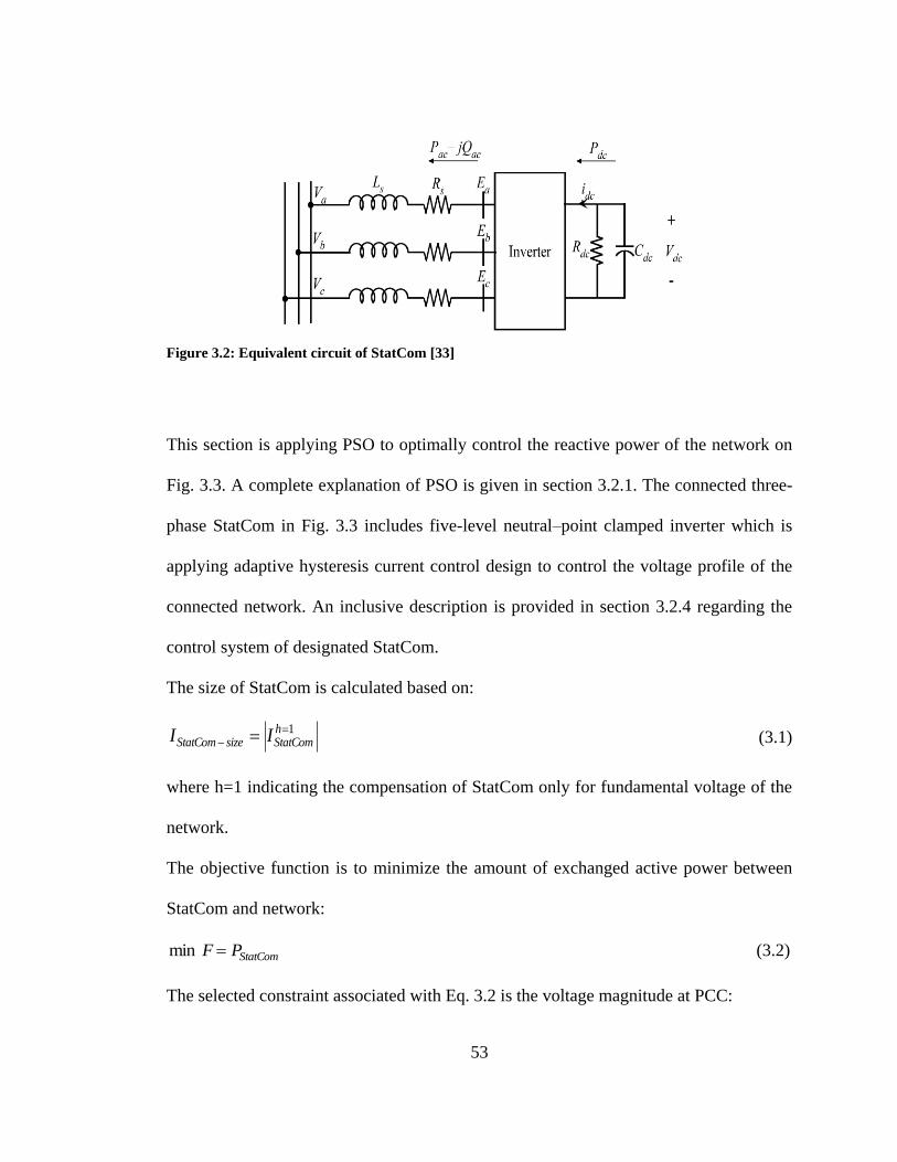
53
Figure 3.2: Equivalent circuit of StatCom [33]
This section is applying PSO to optimally control the reactive power of the network on
Fig. 3.3. A complete explanation of PSO is given in section 3.2.1. The connected three-
phase StatCom in Fig. 3.3 includes five-level neutral–point clamped inverter which is
applying adaptive hysteresis current control design to control the voltage profile of the
connected network. An inclusive description is provided in section 3.2.4 regarding the
control system of designated StatCom.
The size of StatCom is calculated based on:
1 h
StatComsizeStatCom II (3.1)
where h=1 indicating the compensation of StatCom only for fundamental voltage of the
network.
The objective function is to minimize the amount of exchanged active power between
StatCom and network:
StatComPF min (3.2)
The selected constraint associated with Eq. 3.2 is the voltage magnitude at PCC:
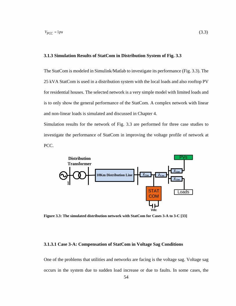
54
puVPCC 1 (3.3)
3.1.3 Simulation Results of StatCom in Distribution System of Fig. 3.3
The StatCom is modeled in Simulink/Matlab to investigate its performance (Fig. 3.3). The
25 kVA StatCom is used in a distribution system with the local loads and also rooftop PV
for residential houses. The selected network is a very simple model with limited loads and
is to only show the general performance of the StatCom. A complex network with linear
and non-linear loads is simulated and discussed in Chapter 4.
Simulation results for the network of Fig. 3.3 are performed for three case studies to
investigate the performance of StatCom in improving the voltage profile of network at
PCC.
Figure 3.3: The simulated distribution network with StatCom for Cases 3-A to 3-C [33]
3.1.3.1 Case 3-A: Compensation of StatCom in Voltage Sag Conditions
One of the problems that utilities and networks are facing is the voltage sag. Voltage sag
occurs in the system due to sudden load increase or due to faults. In some cases, the
Distribution
Transformer
1
10Km Distribution Line
STAT
COMLoads
PVs
ZLine
Vdc
ZLine
ZLine
ZLine

55
voltage deep leads to partial or even full interruption of networks. Therefore, this issue
should be considered to prevent more breaks to the networks. StatCom as a shunt
converter is one of the solutions to mitigate the voltage sags.
Fig. 3.4 shows the simulation results for case 3-A. Fig. 3.4a displays the voltage profile
of StatCom at PCC. As can be seen, the voltage of network is not always one pu. This can
be due to some extra loads on the network. In Fig. 3.4a, the blue line is the voltage profile
of PCC when StatCom is not connected while the black line is the voltage of the same
point when the StatCom is in operation. At t=0.1sec, the network is facing overload
problem and the line voltage drops to 0.95 pu. At t=0.2sec, a very large load is energized
and consequently the network line voltage drops more to 0.8 pu. Then at t=0.3sec, the
network continues on its normal conditions. As can be seen by implementing StatCom,
the network voltage is maintained at one pu at all times (black line). Fig. 3.4b shows the
injected active and reactive power by StatCom. The active power is always close to zero
indicating good performance of PSO in satisfying the requirements of objective function.
From Fig. 3.4b also can be realized that the injected reactive power to the network is
increasing when the voltage of network is dropping. Fig. 3.4c illustrates the line current
of StatCom. It is noticeable that by dropping the network voltage, the StatCom is injecting
more reactive current to the network and the current is close to zero under normal
conditions of the network.

56
(a)
(b)
(c)
Figure 3.4: Simulation results for Case 3-A; (a) network line voltage, (b) injected active and
reactive power of StatCom, (c) StatCom injected current.
0.05 0.1 0.15 0.2 0.25 0.3 0.35 0.4
0.8
0.9
1
1.1
1.2
Time [S]
Netw
ork
Lin
e V
olt
age [
pu
]
Without StatCom
With StatCom
0.05 0.1 0.15 0.2 0.25 0.3 0.35 0.4-2
0
2
4
6
8
10
Time [S]
[kW
] &
[k
VA
R]
Active Power
Reactive Power
0.05 0.1 0.15 0.2 0.25 0.3 0.35 0.4-50
-40
-30
-20
-10
0
10
20
30
40
50
Time [S]
Sta
tCom
Cu
rren
t [A
]
Ia
Ib
Ic

57
3.1.3.2 Case 3-B: Compensation of StatCom in Voltage Swell Conditions
Due to growing the installation of rooftop PVs, the network is facing many problems such
as voltage swell into the distribution networks. StatCom is one of the best solutions to
prevent increase of voltage in distribution networks. Fig. 3.5 presents the simulation
results for this part. Fig. 3.5a shows the voltage of network at PCC. The network voltage
is one pu until t=0.1sec; then the voltage drops to 0.95 pu. After that, at t=0.2sec, the
network voltage is raised to 1.2 pu which is coincided with a sunniest time of the day and
the power flow from the PV to the network causes over-voltage on the system. Finally, at
t=0.3sec, the network continues to its normal conditions. The black line shows the line
voltage at PCC after using the StatCom which is maintained at one pu. The transferred
active power is still zero and the reactive power is changing based on network
requirements (Fig. 3.5b). Until t=0.2sec, the reactive power is injected into the network
but between t=0.2 till 0.3sec, the StatCom is absorbing reactive power from the network
to drop the voltage from 1.2 pu to 1 pu. At t=0.3sec, the StatCom is changed from
capacitive mode to inductive mode. This can also be observed from Fig. 3.5c. This figure
shows the phase shift between voltage and current of the StatCom. Before t=0.2sec, the
StatCom acts as a capacitive load and the current leads the voltage, but after that and until
t=0.3sec, the current lags the voltage and the StatCom performance is like the inductive
load.

58
(a)
(b)
(c)
Figure 3.5: Simulation results for Case 3-B; (a) network line voltage, (b) injected active and reactive
power of StatCom, (c) voltage and current of StatCom
0.05 0.1 0.15 0.2 0.25 0.3 0.35 0.40.9
1
1.1
1.2
Time [S]
Netw
ork
Lin
e V
olt
age [
pu
]
Without StatCom
With StatCom
0.05 0.1 0.15 0.2 0.25 0.3 0.35 0.4-8
-6
-4
-2
0
2
4
Time [S]
[kW
] &
[k
VA
R]
Active Power
Reactive Power
0.12 0.14 0.16 0.18 0.2 0.22 0.24 0.26 0.28-40
-20
0
20
40
60
Time [S]
Volt
age a
nd
Cu
rren
t of
Sta
tCom
[V
& A
]
Current
Voltage
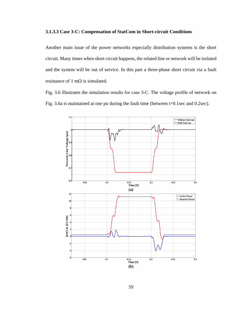
59
3.1.3.3 Case 3-C: Compensation of StatCom in Short-circuit Conditions
Another main issue of the power networks especially distribution systems is the short
circuit. Many times when short circuit happens, the related line or network will be isolated
and the system will be out of service. In this part a three-phase short circuit via a fault
resistance of 1 m is simulated.
Fig. 3.6 illustrates the simulation results for case 3-C. The voltage profile of network on
Fig. 3.6a is maintained at one pu during the fault time (between t=0.1sec and 0.2sec).
(a)
(b)
0.05 0.1 0.15 0.2 0.25 0.30.6
0.7
0.8
0.9
1
1.1
Time [S]
Netw
ork
Lin
e V
olt
age [
pu
]
Without StatCom
With StatCom
0.05 0.1 0.15 0.2 0.25 0.3-6
-4
-2
0
2
4
6
8
10
12
Time [S]
[kW
] &
[k
VA
R]
Active Power
Reactive Power

60
(c)
Figure 3.6: Simulation results for Case 3-C; (a) network line voltage, (b) injected active and reactive
power of StatCom, (c) StatCom injected current
Fig. 3.6b shows how the StatCom injects reactive power to the network during the fault
time. The line current of StatCom is presented in Fig. 3.6c which is zero except during
the fault time.
3.2 Siting and Sizing of StatCom in Balanced and Unbalanced Distribution Networks
StatCom usually generates a balanced set of three-phase sinusoidal voltages at the
fundamental frequency with controllable amplitude and phase angle. Unlike most
conventional reactive power compensators, StatCom facilitates dynamic compensation of
electrical power systems and improves the utilization of existing networks [36].
However, the loads are not always balanced and some industrial loads draw unequal load
currents from the three-phase power system. Large unbalanced loads usually result in
voltage imbalances in the power networks which affect other customers within that
network. Furthermore, many loads such as induction motors are very sensitive to voltage
imbalances and even small voltage imbalances can result in overheating and unbalanced
0.05 0.1 0.15 0.2 0.25 0.3-80
-60
-40
-20
0
20
40
60
80
Time [S]
Sta
tCom
Cu
rren
t [A
]
Ia
Ib
Ic

61
electromagnetic torques. Therefore, it is very important to rectify voltage imbalances in
the networks.
This section explores voltage instability in the distribution system including within local
loads as well as balanced and unbalanced large industrial loads. Thus, illustrating how
StatCom can mitigate the voltage instability problems. Also, particle swarm optimization
(PSO) technique is used for optimally allocation and sizing of StatComs in the distribution
network. Therefore, a brief explanation of PSO is given in the following section.
3.2.1 Particle Swarm Optimization Method
Optimal siting and sizing of FACTS devices in distribution networks is an important
subject in the electrical engineering area. Among different optimization techniques, PSO
is a common optimizer tool for optimal siting and sizing of FACTS devices. In [47] it is
proved that PSO is more accurate compared to non-linear programming and genetic
algorithm [136]. Therefore, PSO is applied to find optimal siting and sizing of StatComs.
It is assumed that StatCom units receive network data from smart meters in a SG with
sophisticated communication networks.
The PSO is an optimization technique based on individual population sizes. Each
individual is referred to as particle and the population is known as a swarm. Each particle
in a swarm should move toward the best position within the population which is the
optimal result. The movement of particles in each iteration is updated by adaptive velocity
(3.4). In each run for PSO, there is an objective function. The best value of this objective
function (minimum answer) for each particle is described as a Pbest and the global best
position among all particles (best Pbest) is represented as a Gbest. Furthermore, the

62
velocity of the particle is determined based on the relative location from Pbest and Gbest
[137]:
)(22
)(11
1 nj
XngbestCnj
Xnj
pbestCnj
Vnj
V (3.4)
where 𝑉𝑗𝑛 and 𝑋𝑗
𝑛 are the velocity and location of particle j at iteration n, respectively.
is the inertia weight factor, 1 and
2 are random numbers between 0 and 1 and
1C and
2C are called the acceleration factors.
3.2.2 Problem Formulation of Siting and Sizing of StatCom
The total size of StatComs connected to the network can be expressed as:
KkIIK
k
h
StatComksizeStatCom ...,,1,1
1
,
(3.5)
where k and h are the bus number and the harmonic order respectively while K represents
the maximum number of buses.
The objective function (OF) for optimal siting and sizing of StatComs is to minimize their
sizes:
sizeStatComIOF min (3.6)
The selected constraints associated with (3.6) are the lower limit of voltage magnitude
(|V|) for each bus according to the Australian standard [138] and also the maximum size
of StatCom (max,kI ):
puk 9.0 |V| (3.7)

63
max,1
,, kh
StatComksizeStatComk III
(3.8)
where k |V| is the voltage magnitude of bus k.
A PSO technique is used to solve (3.5)-(3.8). The fundamental current of StatCom
consists of both magnitude and phase angle. Therefore, each magnitude and phase angle
of the StatCom current at each bus are assigned as the position of a particle during the
optimization process. The first step of this optimization is to specify the system input data
including all load data and system configurations such as the voltage of all buses and the
maximum current of StatCom. The PSO factors and iterations are also determined in this
step. Then one particle is allotted for each magnitude and each phase angle of StatCom
current at all buses. The next stage is to determine the optimal locations and sizes of
StatComs. Therefore, the PSO runs the Simulink file and returns the values for voltage of
all buses and the sizes of StatComs. Then, based on this data and (3.4)-(3.8), the current
of StatCom at each bus is calculated.
3.2.3 System Specifications of 15-Bus Test System
To assess the effectiveness of the proposed approach, optimal placement and sizing of
three-phase StatComs will be performed for the 15-bus radial power system of Fig. 3.7
[139]. The system contains four large loads located at buses 5, 7, 10 and 13. The detailed
specifications of this system are presented in Tables 3.1 and 3.2.

64
1 2 3 4 56
9
7
10
11
12
13
14
15
8
Big Load 1
Big Load 2
Big Load 3
Big Load 4
Figure 3.7: The 15-bus test system [139] including local loads and four large loads
Table 3.1: Line data of the network in Fig. 3.7
Branch From Bus To Bus R (ohm) X (ohm)
1 1 2 1.35309 1.32349
2 2 3 1.17024 1.14464
3 3 4 0.84111 0.82271
4 4 5 1.52348 1.02760
5 2 9 2.01317 1.35790
6 9 10 1.68671 1.13770
7 2 6 2.55727 1.72490
8 6 7 1.08820 0.73400
9 6 8 1.25143 0.84410
10 3 11 1.79553 1.21110
11 11 12 2.44845 1.65150
12 12 13 2.01317 1.35790
13 4 14 2.23081 1.50470
14 4 15 1.19702 0.80740
Table 3.2: Linear load data of the network in Fig. 3.11
Bus KVA Bus KVA Bus KVA
1 0 6 200 11 200
2 63 7 200 12 100
3 100 8 100 13 63
4 200 9 100 14 100
5 63 10 63 15 200

65
3.2.4 Three-Phase StatCom with Five-Level NPC Inverter
The StatCom inverters are designed with the five level neutral-point clamped (FL-NPC)
configuration [34] [140]. The topology of a three-phase FL-NPC inverter supplying a
series RL impedance (filter𝑅𝑓 and 𝐿𝑓impedances) and an ac back EMF (𝑣𝑎𝑏𝑐) is shown
in Fig. 3.8. Five output voltage levels can be integrated by this structure including
0, ±𝑉𝑑𝑐/4 and ±𝑉𝑑𝑐/2.
3.2.4.1 Adaptive Hysteresis Current Control Design
For the StatCom inverter, an adaptive hysteresis current control (AHCC) approach is used
[36]. Assuming that the grounded neutral point of the system is connected to the midpoint
of the FL-NPC inverter and applying KVL for phase-a:
aStatComafStatComafa vidt
dLiRu (3.9)
where 𝑣𝑎, 𝑖StatCom 𝑎, 𝑢𝑎 are the phase-a PCC voltage (ac side), the phase-a inverter output
current (or StatCom output current) and the phase-a inverter output voltage (dc side),
respectively.
To maintain the switching frequency constant, the fundamental components of the
inverter output voltages is used to adjust the hysteresis bands instead of using the system
parameters. If the phase-a leg of the FL-NPC inverter (shown in Fig. 3.8) is assigned to
generate and inject 𝑖𝑆𝑡𝑎𝑡𝐶𝑜𝑚𝑎 at PCC, then the inverter must generate a voltage greater
than the PCC voltage.

66
Filter PCC
Sa1
Sa2
Sa3
Sa4
Sa1
Sa2
Sa3
Sa4
Sb1
Sb2
Sb3
Sb4
Sc1
Sc2
Sc3
Sc4
Sb1
Sb2
Sb3
Sb4
Sc1
Sc2
Sc3
Sc4
Lf Rf
i (a
bc
)
vabc
ua
ub
uc
n
C1
C2
C3
C4
Vdc1
Vdc2
Vdc3
Vdc4
Figure 3.8: Detailed FL-NPC inverter structure of the shunt FACTS devices [140]
For the ideal case, the inverter creates the blue sinusoidal voltage waveform of Fig. 3.9a;
however, in reality the red non-sinusoidal waveform is produced since the inverter utilizes
a modulation technique. As a result, the actual modulated current will include two
components related to the created realistic voltage including fundamental (𝑖𝑠𝑆𝑡𝑎𝑡𝐶𝑜𝑚−𝐹)
and switching ripple (𝑖𝑇𝐻𝑆𝑡𝑎𝑡𝐶𝑜𝑚−𝑅) components:
RStatComFStatComStatCom iii (3.10)
Assuming the voltage drop caused by the switching ripple across 𝑅𝑓 is considerably less
than across 𝐿𝑓 and substituting Eq. 3.10 into Eq. 3.9:
f
ideala
f
aFStatComadt
dfai
L
avu
L
viLu
dt
dRStatCom
(3.11)
where 𝑣𝑖𝑑𝑒𝑎𝑙−𝑎 is the fundamental component of the inverter output voltage for phase-a.
As realized in Fig. 3.9a, there are four different areas (Area 1-4) depending on the ideal
voltage value. Based on this figure, the following switching periods are obtained:

67
).4/)(2/(
2(
4
)4/
2(
1
4
)4/)(2/(
2(
4
)4/
2(
1
4
44
33
22
11
dcaidealaidealdc
fadca
aidealdc
fa
aideal
dca
dcaidealaidealdc
fadca
aidealdc
fa
aideal
dca
VvvV
LhVT
vV
Lh
v
VT
VvvV
LhVT
vV
Lh
v
VT
(3.12)
According to Figs. 3.9b-e, the switching periods for Areas 1-2 and Areas 2-4 are similar.
Therefore, we need to have 𝑇1 = 𝑇3 = 1/𝑓𝑠𝑤 and 𝑇2 = 𝑇4 = 1/𝑓𝑠𝑤 in order to maintain
a constant switching frequency. Using Eq. 3.12, we have:
)14/
)(4/
2(
)4/
1(4/
max2442
max1331
dc
aideal
dc
aidealaaa
dc
aideal
dc
aidealaaa
V
v
V
vhhhh
V
v
V
vhhhh
(3.13)
where ℎ𝑎13𝑚𝑎𝑥 = 𝑉𝑑𝑐/(8𝐿𝑓𝑓𝑠𝑤).
3.2.4.2 Selection of Hysteresis Band Shape
Based on Eq. 3.13, depending on the amplitude of the fundamental component of the
inverter output voltage and the absolute value of the ideal voltage, there are two hysteresis
band shapes that must be properly selected for the correct AHCC operation with a constant
switching frequency. The key for the selection between the hysteresis shapes is the margin
voltage level of 𝑉𝑑𝑐/4. The difference between ideal and margin voltages specifies the
beginning and end of utilization of hysteresis shapes. Hence, the following equation is
derived for the transition between the two band shapes:
4/dcidealtrans VavT (3.14)

68
where 𝑇𝑡𝑟𝑎𝑛𝑠 is the transition time between ℎ𝑎13 and ℎ𝑎24. Fig. 3.10 shows the hysteresis
band shapes obtained from Eq. 3.13 which are controlled and selected by Eq. 3.14. The
switching between the two shapes to construct the whole hysteresis band ℎ𝑎 is organized
by 𝑇𝑡𝑟𝑎𝑛𝑠. During time intervals corresponding to Ttrans < 0, the ha13 activation pulse is
changed from zero to one (red pulse in Fig. 3.10) and the control system designates ha13
for the hysteresis band, otherwise ha24 is used.
t1 t2 t3 t4 t5 t6 t7
Videal-a
Inverter Phase Voltage
Area 1
Area 2
Area 3
Area 4
Vdc /4
Vdc /2
-Vdc /4
-Vdc /2
0
(a) Ideal voltage
ton1 toff1
0
1
-h
+h
Vdc /4
0
Sa2
IStatComa-R
ua
Switching Signal
Ripple Current
Inverter Voltage
t1 t2Area 1 T1a=ton1+toff1
0
1
-h
+h
Vdc /2
Sa1
IStatComa-R
ua
Switching Signal
Ripple Current
Inverter Voltage
t2 t3Area 2 T2a=ton2+toff2
Vdc /4
ton2toff2
(b) Area 1 (c) Area 2
0
1
-h
+h
-Vdc /40
Sa3
IStatComa-R
ua
Switching Signal
Ripple Current
Inverter Voltage
Switching Signal
Ripple Current
Inverter Voltage
t4 t5Area 3 T3a=ton3+toff3
toff3 ton3
0
1
-h
+h
-Vdc /4
Sa4
IStatComa-R
ua
Switching Signal
Ripple Current
Inverter Voltage
t5 t6Area 4 T4a=ton4+toff4
-Vdc /2
toff4ton4
(d) Area 3 (e) Area 4
Figure 3.9: The APLC generated FL-NPC inverter voltage using HCC; (a) ideal (blue) and actual
(red) waveforms, (b)-(e) detailed waveforms for Areas 1 to 4 [140]:
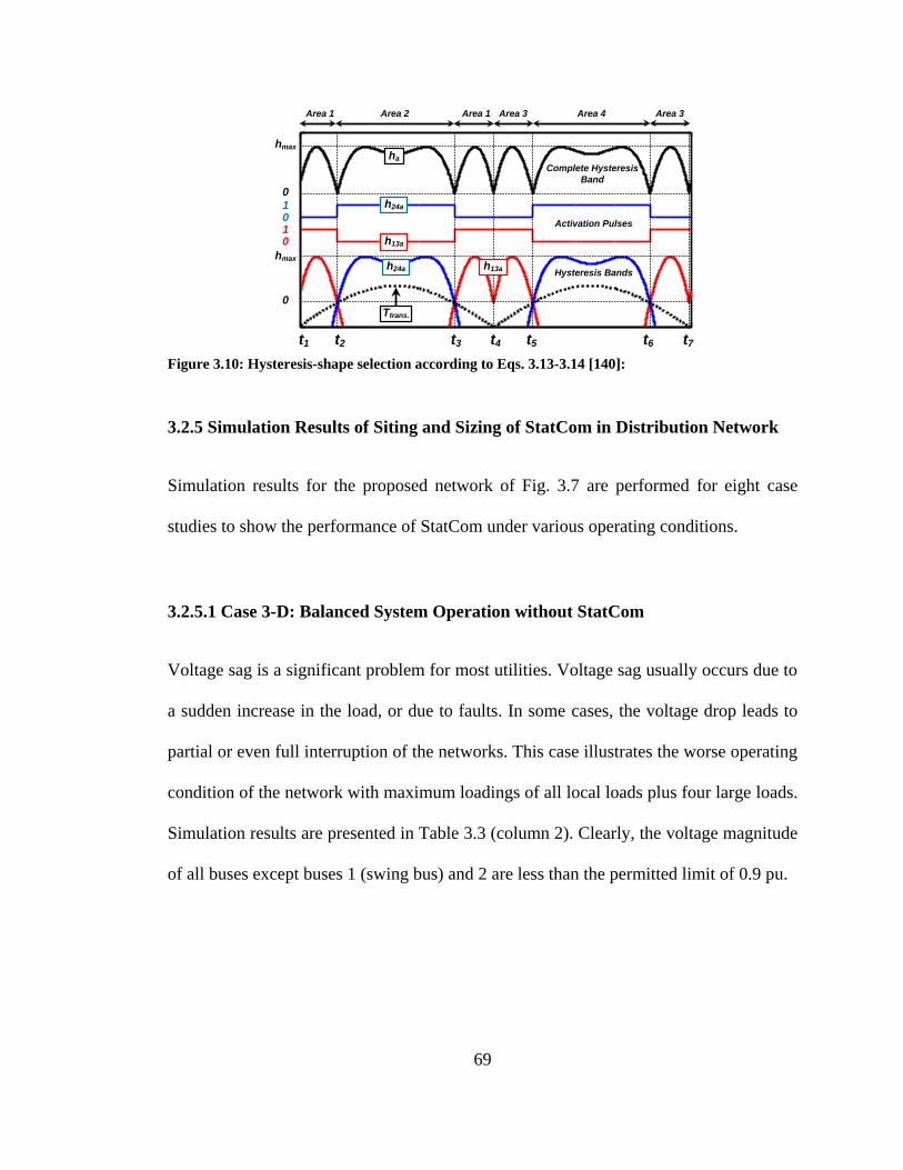
69
t1 t2 t3 t4 t5 t6 t7
Activation Pulses
Complete Hysteresis
Band
Hysteresis Bands
Ttrans.
hmax
0
01
01
h13a
h24a
ha
0
h13ah24a
hmax
Area 1 Area 2 Area 1 Area 3 Area 4 Area 3
Figure 3.10: Hysteresis-shape selection according to Eqs. 3.13-3.14 [140]:
3.2.5 Simulation Results of Siting and Sizing of StatCom in Distribution Network
Simulation results for the proposed network of Fig. 3.7 are performed for eight case
studies to show the performance of StatCom under various operating conditions.
3.2.5.1 Case 3-D: Balanced System Operation without StatCom
Voltage sag is a significant problem for most utilities. Voltage sag usually occurs due to
a sudden increase in the load, or due to faults. In some cases, the voltage drop leads to
partial or even full interruption of the networks. This case illustrates the worse operating
condition of the network with maximum loadings of all local loads plus four large loads.
Simulation results are presented in Table 3.3 (column 2). Clearly, the voltage magnitude
of all buses except buses 1 (swing bus) and 2 are less than the permitted limit of 0.9 pu.

70
3.2.5.2 Case 3-E: Siting and Sizing of StatComs in Balanced System
The PSO is used to find the optimal locations and sizes of the StatComs for the 15-bus
network of Fig. 3.7. Simulation results are summarized in Table 3.3 (columns 3-4).
As a result, just one StatCom is allocated at bus 11 to compensate the voltage drops of the
network. To maintain the voltage of all buses at the minimum value of 0.9 pu, one
StatCom with the size of 0.260 pu is needed at bus 11.
3.2.5.3 Case 3-F: Siting and Sizing of StatComs with an Additional Constraint for
Maximum Size of StatComs (0.15 pu) in Balanced System
In practice, utilities may also require a maximum limit for the StatCom rating. This can
be accomplished by repeating the simulation of Case 3-E with an additional constraint for
the maximum size of StatComs which is selected to be 0.15 pu (3.13). In this case two
StatComs are nominated to be allocated at buses 3 and 13 with sizes of 0.15 pu and 0.114
pu, respectively, with the total StatCom size of 0.264 pu. The results are illustrated in
Table 3.3 (columns 5-6).
3.2.5.4 Case 3-G: Siting and Sizing of StatComs with an Additional Constraint for
Maximum Size of StatComs (0.10 pu) in Balanced System
This case is identical to case 3-F with the different constraint on maximum sizing of
StatCom (0.1 pu). In this case, 3 StatComs are located at buses 4, 6 and 13 with sizes of
0.085, 0.029 and 0.096, respectively; with the total StatCom size of 0.210 pu as illustrated
in Table 3.3 (columns 7-8).
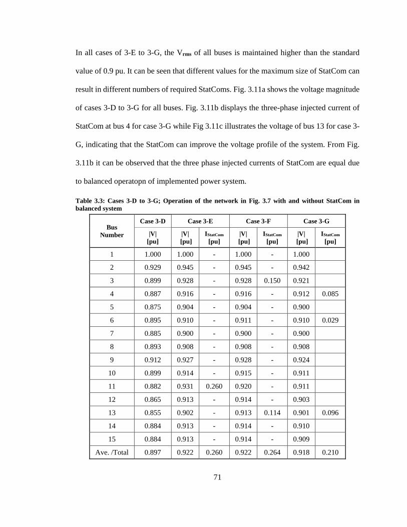
71
In all cases of 3-E to 3-G, the Vrms of all buses is maintained higher than the standard
value of 0.9 pu. It can be seen that different values for the maximum size of StatCom can
result in different numbers of required StatComs. Fig. 3.11a shows the voltage magnitude
of cases 3-D to 3-G for all buses. Fig. 3.11b displays the three-phase injected current of
StatCom at bus 4 for case 3-G while Fig 3.11c illustrates the voltage of bus 13 for case 3-
G, indicating that the StatCom can improve the voltage profile of the system. From Fig.
3.11b it can be observed that the three phase injected currents of StatCom are equal due
to balanced operatopn of implemented power system.
Table 3.3: Cases 3-D to 3-G; Operation of the network in Fig. 3.7 with and without StatCom in
balanced system
Bus
Number
Case 3-D Case 3-E Case 3-F Case 3-G
|V| [pu]
|V| [pu]
IStatCom
[pu]
|V| [pu]
IStatCom
[pu]
|V| [pu]
IStatCom
[pu]
1 1.000 1.000 - 1.000 - 1.000
2 0.929 0.945 - 0.945 - 0.942
3 0.899 0.928 - 0.928 0.150 0.921
4 0.887 0.916 - 0.916 - 0.912 0.085
5 0.875 0.904 - 0.904 - 0.900
6 0.895 0.910 - 0.911 - 0.910 0.029
7 0.885 0.900 - 0.900 - 0.900
8 0.893 0.908 - 0.908 - 0.908
9 0.912 0.927 - 0.928 - 0.924
10 0.899 0.914 - 0.915 - 0.911
11 0.882 0.931 0.260 0.920 - 0.911
12 0.865 0.913 - 0.914 - 0.903
13 0.855 0.902 - 0.913 0.114 0.901 0.096
14 0.884 0.913 - 0.914 - 0.910
15 0.884 0.913 - 0.914 - 0.909
Ave. /Total 0.897 0.922 0.260 0.922 0.264 0.918 0.210

72
(b)
(c)
Figure 3.11: Simulation results of StatCom in the balanced network; (a) |V| of buses for a network
of Fig. 3.7 for cases 3-D to 3-G, (b) injected current of StatCom at bus 4 for case 3-G, (c) voltage
profile of bus 13 with and without StatCom for case 3-G
0.84
0.86
0.88
0.9
0.92
0.94
0.96
0.98
1
1 2 3 4 5 6 7 8 9 10 11 12 13 14 15
Vo
lta
ge
[pu
]
Bus Number
(a)
3-D 3-E 3-F 3-G
0.02 0.025 0.03 0.035 0.04 0.045 0.05 0.055 0.06-0.2
-0.15
-0.1
-0.05
0
0.05
0.1
0.15
Time [s]
Inje
cte
d C
urren
t of
Sta
tCom
at
Bu
s 4 [
pu
]
Phase A
Phase B
Phase C
0.02 0.025 0.03 0.035 0.04 0.045 0.05 0.055 0.06-1
-0.5
0
0.5
1
Time [s]
Volt
age o
f B
us
13 [
pu
]
Without StatCom
With StatCom

73
In all these cases the simulations are performed in a balanced network. However, there
are sometimes large unbalanced industrial loads which lead to an imbalanced power
network. Cases 3-H to 3-K investigate the operation of StatCom in unbalanced load
conditions.
3.2.5.5 Cases 3-H and 3-J; Unbalanced System Operation without StatCom
The voltage magnitudes of network buses of Fig. 3.7 are presented in Tables 3.4 and 3.5
for Cases 3-H and 3-J, respectively. These cases present the voltage profile of network
without employing StatComs under two different unbalanced operating conditions. The
variation of voltage magnitude values between Cases 3-H and 3-J is executed due to the
dissimilarity of unbalanced loads.
3.2.5.6 Cases 3-I and 3-K; Siting and Sizing of StatComs in an Unbalanced Network
The simulation of these cases resulted into allocation of two StatComs at buses 3 and 13.
Tables 3.4-3.5 and Figs. 3.12-3.13 show the simulation results for these cases.
Before t=0.1sec, the network data are selected based on case 3-H. At t=0.1sec, the network
switched to case 3-J. As can be seen from Fig. 3.12, in both cases the StatComs maintained
the voltage magnitude of all buses at the minimum value of 0.9 pu by injecting unequal
three-phase fundamental currents (Figs. 3.13b and 3.13c). Fig. 3.13a displays the voltage
profile of bus 13 with and without StatCom for three phases. Figs. 3.13b and 3.13c
illustrate the three-phase injected currents of StatCom at buses 3 and 13, respectively. It

74
is observed that due to the operation of unbalanced loads and based on Eqs. 3.6 and 3.7,
the injected currents of StatComs for each phase are unequal.
Table 3.4: Cases 3-H and 3-I; Operation of the network in Fig. 3.7 with and without StatCom in
unbalanced system
Bus Number
Case 3-H Case 3-I
|V|a
[pu]
|V|b
[pu]
|V|c
[pu]
|V|a
[pu]
|V|b
[pu]
|V|c
[pu]
IStatCom
[pu]
1 1.000 1.000 1.000 1.000 1.000 1.000
2 0.913 0.935 0.949 0.960 0.943 0.951
3 0.876 0.906 0.925 0.967 0.921 0.929 0.257
4 0.862 0.895 0.917 0.951 0.910 0.920
5 0.847 0.886 0.912 0.935 0.900 0.915
6 0.870 0.904 0.925 0.915 0.912 0.927
7 0.856 0.896 0.919 0.900 0.903 0.921
8 0.868 0.902 0.922 0.913 0.909 0.924
9 0.891 0.921 0.940 0.937 0.928 0.942
10 0.874 0.910 0.934 0.919 0.918 0.936
11 0.856 0.890 0.911 0.948 0.914 0.917
12 0.833 0.872 0.896 0.928 0.909 0.906
13 0.818 0.862 0.888 0.915 0.910 0.900 0.070
14 0.860 0.893 0.915 0.949 0.907 0.918
15 0.860 0.893 0.914 0.949 0.907 0.918
Ave. /Total 0.872 0.904 0.924 0.939 0.919 0.928 0.327

75
Table 3.5: Cases 3-J and 3-K: Operation of the network in Fig. 3.7 with and without StatCom in
unbalanced system
Bus Number
Case 3-J Case 3-K
|V|a
[pu]
|V|b
[pu]
|V|c
[pu]
|V|a
[pu]
|V|b
[pu]
|V|c
[pu]
IStatCom
[pu]
1 1.000 1.000 1.000 1.000 1.000 1.000
2 0.935 0.949 0.913 0.943 0.951 0.960
3 0.906 0.925 0.876 0.921 0.929 0.967 0.277
4 0.895 0.917 0.862 0.910 0.920 0.951
5 0.886 0.912 0.847 0.900 0.915 0.935
6 0.904 0.925 0.870 0.912 0.927 0.915
7 0.896 0.919 0.856 0.903 0.921 0.900
8 0.902 0.922 0.868 0.909 0.924 0.912
9 0.921 0.940 0.891 0.928 0.942 0.937
10 0.910 0.934 0.874 0.918 0.936 0.919
11 0.890 0.911 0.856 0.914 0.917 0.947
12 0.872 0.896 0.833 0.909 0.906 0.925
13 0.862 0.888 0.818 0.909 0.900 0.912 0.067
14 0.893 0.915 0.860 0.907 0.918 0.949
15 0.893 0.914 0.860 0.907 0.918 0.949
Ave. /Total 0.904 0.924 0.872 0.919 0.928 0.939 0.344
Figure 3.12: |V| of all buses for cases 3-I and 3-K Simulation in unbalanced network of Fig 3.7
0.05 0.1 0.15 0.2 0.250.88
0.9
0.92
0.94
0.96
0.98
1
Time [s]
Vrm
s of
Ph
ase
A o
f A
ll B
use
s [p
u]

76
(a)
(b)
(c)
Figure 3.13: Simulation results of StatCom in unbalanced network of Fig 3.7; (a) voltage profile of
bus 13 with and without StatComs for cases 3H to 3-K, (b) injected current of StatCom at bus 3 for
cases 3-I and 3-K, (c) injected current of StatCom at bus 13 for cases 3-I and 3-K
0.05 0.06 0.07 0.08 0.09 0.1 0.11 0.12 0.13 0.14
-1-0.9
-0.5
0
0.5
0.91
Time [s]
Volt
age
of
Bu
s 13 [
pu
]
Phase A With StatCom Phase B With StatCom Phase C With StatCom Phase A Without StatCom Phase B Without StatCom Phase C Without StatCom
0.05 0.06 0.07 0.08 0.09 0.1 0.11 0.12 0.13 0.14
-1
-0.5
0
0.5
1
Time [s]
Inje
cted
Cu
rren
t of
Sta
tCom
atB
us
3 [
pu
]
Phase A
Phase B
Phase C
0.05 0.06 0.07 0.08 0.09 0.1 0.11 0.12 0.13 0.14
-1
-0.5
0
0.5
1
Time [s]
Inje
cted
Cu
rren
t o
f S
tatC
om
at
Bu
s 1
3 [
pu
]
Phase A
Phase B
Phase C

77
CHAPTER 4: OPTIMAL SITING AND SIZING OF MULTIPLE
APLCS FOR FUNDAMENTAL AND HARMONIC VOLTAGE
COMPENSATION
The reactive power and harmonic compensation can be achieved by using shunt FACTS
devices. Usually, StatCom can be used for reactive power compensation (Chapter 2) while
APF compensate harmonic distortions. As mentioned before, APFs compensate 100% of
nonlinear load harmonics and improve the power quality of power systems. However, this
approach needs one APF for each nonlinear load which is not economical. Therefore,
APLC as a custom power device is proposed to reduce the harmonics of the entire network
to meet the minimum requirements of network specified by IEEE Standard 519-1992 [38].
Most of the researches are based on compensating only reactive power or voltage
harmonic distortions of the network. However, some of them try to compensate both the
reactive power and voltage harmonics together [141-146]. In [141] the APF is designed
to provide reactive power and harmonics compensation for linear and non-linear single-
phase loads. [142] proposes universal active filter topology for single-phase systems
applications without transformer with a combination of parallel and series active filters.
In [143-146] they talk about StatCom with harmonic elimination capability. In other
publications [147-150] a custom power device consists of series and shunt converter
called UPQC is investigated to compensate the line current distortion and also maintain
the bus voltage.
All mentioned publications compensate the voltage and harmonic distortion of only one
load at PCC. Just [147] considers compensation of entire network and discussed the

78
allocation of UPQC in the radial distribution network. However, in [147] only the reactive
power compensation of a distribution network is considered and the UPQCs based on
three objectives functions of rating of UPQC, network power loss and percentage of nodes
with under-voltage problem are allocated.
This chapter compensates both the reactive power and harmonic distortion of entire radial
distribution network by using just shunt APLC. It proposes two PSO-based algorithms for
optimal siting (placement), sizing (rating) and online control (operation) of multiple
APLCs in distorted SGs that rely on smart meter recorded and transmitted data. The
objective function consists of minimization of the overall network THDv and total APLC
injected current while the constraints include the fundamental voltage (VFund) of each bus,
network THDv and individual bus voltage harmonics with an optional limit for the
maximum APLC sizes. Detailed simulations are presented and analyzed for the 15-bus
network of [139] with six nonlinear loads. The impacts of the weighting factors in the
objective function for APLC size and THDv as well as the effect of including an upper
limit for APLC ratings are also investigated.
4.1 Modelling for Optimal Siting and Sizing of APLC for Fundamental and
Harmonic Voltage Compensation
The APLCs are modeled as decoupled harmonic current sources injecting harmonic
currents at PCCs. This section proposes a PSO-based algorithm for optimal siting and
sizing of multiple APLCs. The size of an APLC connected to bus k can be expressed as
[37-48]:
79
HhKkII
III
H
h
hAPLCkAPLCk
harmonicsAPLCklfundamentaAPLCksizeAPLCk
...,,2,...,,1,2
2
,1
,
,,,
(4.1)
where k and h are the bus number and the harmonic order while K and H represent their
maximum values, respectively.
The objective function for optimal siting and sizing of APLCs is to minimize their sizes
and the overall network THDv:
K
k
k
H
h
hkTHD
K
k
sizeAPLCksize
networkvTHDsizesAPLCsize
VVWIW
THDWIWF
1
1
2
2
1
, /
min
(4.2)
where 𝑊𝑠𝑖𝑧𝑒 and 𝑊𝑇𝐻𝐷 are the weighting factors for APLC size and network THDv
while 𝑉𝑘1 and 𝑉𝑘
ℎ represent the fundamental and harmonic voltages at bus k, respectively.
The selected constraints associated with Eq. 4.2 are lower limit for VFund, the upper limits
for the THDv and individual voltage harmonics of each bus according to the IEEE-519
standard [37-38]:
pukFundV 9.0 (4.3)
05.0/ lim,
1
2
2
,
itbusvk
H
h
hkkv THDVVTHD (4.4)
03.0/lim1
it
buskh
k VVV (4.5)
where kFundV is the fundamental voltage of bus k.
A PSO algorithm is used to solve Eqs. 4.2-4.5. The proposed PSO algorithm for siting
and sizing of APLCs is demonstrated in the flowchart of Fig. 4.1a. Based on this figure,
an APLC unit is installed temporarily at each bus except the swing bus and then PSO

80
performs an optimization solution for Eqs. 4.1 to 4.5. At the last step, APLCs with sizes
greater than a desired lower limit (e.g., 𝐼𝑚𝑖𝑛,𝐴𝑃𝐿𝐶 𝑠𝑖𝑧𝑒= 0.01pu) are selected.
4.2 Optimal Online Operation of APLCs for Fundamental and Harmonic Voltage
Compensation
The problem formulation for online control of APLCs based on the received smart meter
data at each APLC bus is similar to Eqs. 4.1-4.5 with the following differences (Fig. 4.1b):
APLCs are only installed at the optimal locations determined by the first PSO algorithm
(Fig. 4.1a) of Section 4.1.
Network status and optimization of the objective function are updated at time steps ∆t
for the period of 24 hours:
...,3,2,;)(
)](/)([)(min
1
,
1
1
2
2
ttttfortIW
tVtVWtF
K
k
sizeAPLCksize
K
k
k
H
h
hkTHD
(4.6)
An additional constraint is included for the maximum sizes of the installed APLCs
according to their ratings:
max,
1
2
, m
H
h
hmsizeAPLCm III
(4.7)
where m and 𝐼𝑚,𝑚𝑎𝑥 are the optimal locations and ratings of APLCs as determined by
the first PSO algorithm.
The flowchart of the second PSO algorithm is shown in Fig. 4.1b. It consists of the
following main steps:

81
1) The optimal number, locations and ratings of the required APLCs are determined based
on the first PSO algorithm of Fig. 4.1a. The APLCs are installed at the selected optimal
locations (buses).
2) The SG central control (SGCC) receives the recorded information by smart meters
through the communication network on online basis with time steps of t, executes the
second PSO algorithm of Fig. 4.1b, and sends the optimal inverter reference currents
to the APLCs. The value of t depends on SG communication design and the required
time to transmit data to SGCC and APLCs.
P
SO
sizing
of A
PL
Cs
Tem
po
rary
alloca
tion
o
f APL
Cs
at all bu
ses
Sele
ction
of o
ptim
al A
PL
C lo
catio
ns
Op
timal sitin
g an
d siz
ing
of A
PL
Cs u
sing
PS
O
Place an APLC with optimal size at bus k
stopk=k+1
Define PSO particles for magnitude and phase angle of each APLC harmonic current
yes
no
yesno
yes
noIteration = Max Iteration?
APLC Size > Min Size?
k=K ?
n=n+1
Allocate an APLC at each bus except the swing bus
Input system & PSO parameters, limits of THDv & voltage harmonics
Run the first PSO (Eqs. 4.2-4.5) to calculate
optimal APLC size for each bus
Co
nn
ectio
n
of o
ptim
ally
sited
and
size
d A
PL
Cs
op
eratio
n
of A
PL
Cs
SG
CC
determ
ines o
ptim
al A
PL
C refere
nce c
urren
ts
Send optimal reference currents to APLCs nodes
stop
Define PSO particles for each APLC harmonic current
yesno
SGCC runs second PSO (Eqs. 4.3-4.7) to calculate optimal
APLC reference currents
t=24 hours?
Connect the selected APLCs by Fig. 4.1a with optimal ratings at their
optimal locations (buses)
Input system & PSO parameters, limites of THDv & voltage harmonics
Update system information (send smart meter data to SGCC)
t=t+t
APLC inverters generate and inject compensating currents
(a) (b)
Figure 4.1: Flowchart of the proposed PSO algorithm for fundamental and harmonic voltage
compensation; (a) optimal siting and sizing of multiple APLCs based on Eqs. 4.1-4.5, (b) optimal
online control of the installed APLCs based on Eqs. 4.3-4.7

82
4.3 Simulation Results
To assess the performance of the proposed approaches for optimal siting, sizing and online
operation of APLCs, the 15-bus, 60 Hz radial network of Fig. 4.2 is considered [139].
System line and load parameters are presented in Tables 3.1-3.2. There are six nonlinear
loads connected to buses 5, 7, 8, 10, 13, and 15. Decoupled harmonic current sources are
used for the nonlinear load modeling (Table 4.1). Each nonlinear load is modeled with
decoupled harmonic current sources injecting harmonic currents that are equal to the
current distortions of the exact model (three-phase full wave resistive rectifier) with rated
sinusoidal voltage excitation. Therefore, the injected current harmonics are fixed and
independent of system operating conditions (not considering harmonic couplings). The
selected values for base power and base voltage are 2.5MVA and 11 kV. The optimal
siting and sizing simulations are performed for the worse scenario with maximum linear
and non-linear loading conditions.
1 2 3 4 56
78
9
10
11
12
13
14
15
Nonlinear Load 5
Nonlinear Load 4
Nonlinear Load 1
Nonlinear Load 6
Nonlinear Load 2Nonlinear Load 3
Figure 4.2: Single-line diagram of the 15-bus distorted system [139] with six nonlinear loads (Tables
3.1-3.2)

83
Four study cases are simulated and the results are presented in Tables 4.2-4.9. These cases
include: 1) system operation without APLCs (Case 4-A), 2) optimal siting/sizing of
APLCs (Case 4-B), 3) optimal siting/sizing of APLCs considering a maximum APLC
current of 0.15pu (Case 4-C) and 4) optimal siting/sizing of APLCs considering a
maximum APLC current of 0.1pu (Case 4-D).
Table 4.1: Current harmonic injection of the nonlinear loads (in percentage of the fundamental
component) in the network of Fig. 4.2
Harmonic Order of The Approximated
Decoupled Model
Harmonic order 5 7 11 13 17 percentage of the harmonic order
to fundamental component [%] 22.60 11.34 9.02 6.49 5.63
4.3.1 System Operation without APLCs (Case 4-A)
This case illustrates the worse operating condition of the network with maximum loadings
of all linear and nonlinear loads. Simulation results for this case are presented in Table
4.2 for individual voltage harmonics (columns 2-6), THDv (column 7) and VFund (column
8) of all buses. Fig. 4.3 also illustrates the individual harmonic distortions and THDv of
Case 4-A.
Figure 4.3: Simulation results for Case 4-A (operation of the network in Fig. 4.2 without any APLCs,
Table 4.2)
0
2
4
6
8
10
12
14
16
18
20
22
24
2 3 4 5 6 7 8 9 10 11 12 13 14 15
%
Bus Number
h5 h7 h11 h13 h17 THDv

84
Table 4.2: Case 4-A; Operation of the network in Fig. 4.2 without any APLCs
Bus
Number
Case 4-A
Harmonic Voltage Distortion (%) THDv
[%]
VFund
[pu] 5 7 11 13 17
2 5.35 3.70 4.50 3.77 4.13 9.69 0.925
3 7.94 5.48 6.66 5.58 6.11 14.34 0.891
4 9.23 6.38 7.75 6.49 7.10 16.69 0.877
5 10.07 6.95 8.44 7.07 7.74 18.19 0.869
6 8.13 5.60 6.80 5.70 6.26 14.67 0.883
7 8.72 6.00 7.30 6.11 6.71 15.74 0.875
8 8.88 6.12 7.43 6.23 6.84 16.03 0.873
9 6.40 4.42 5.37 4.50 4.94 11.58 0.911
10 7.31 5.04 6.13 5.14 5.64 13.21 0.901
11 8.96 6.18 7.50 6.28 6.87 16.17 0.874
12 10.42 7.17 8.71 7.29 7.97 18.77 0.854
13 11.66 8.02 9.73 8.15 8.91 20.99 0.842
14 9.23 6.38 7.75 6.49 7.10 16.69 0.875
15 9.96 6.88 8.35 7.00 7.66 18.00 0.868
Ave.
/Total 8.73 6.02 7.32 6.13 6.71 15.77 0.880
Clearly, the entire network is highly distorted, the THDv of all buses are greater than the
permitted limit of 5% and the voltage harmonics of most buses are above the acceptable
level of 3%. Moreover, the fundamental voltage (VFund) of most buses is less than the
standard value of 0.9 pu. Bus 13 is the worst distorted point of the network (Table 4.2,
Fig. 4.3) due to its remote location from bus 1. This is the farthest bus from the swing bus
(e.g., the higher line impedance) with the THDv and VFund values of 20.99% and 0.84 pu,
respectively.

85
4.3.2 Optimal Siting and Sizing of Multiple APLCs (Case 4-B) for Fundamental and
Harmonic Voltage Compensation
The PSO algorithm of Fig. 4.1a is used to find the optimal locations and sizes of the
APLCs for the 15-bus network of Fig. 4.2. Simulation results are summarized in Table
4.3. The values of weighting factors in Eq. 4.6 are selected to be WTHD = 0.5 and Wsize
=0.5. Section 4.3.2.1 investigates the impacts of weighting factors on the optimal siting
and sizing of multiple APLCs.
Table 4.3: Case 4-B; Optimal siting and sizing of multiple APLCs for the network of Fig. 4.2 for
fundamental and harmonic voltage compensation
Bus
Number
Case 4-B
Harmonic Voltage Distortion (%) THDv
(%)
VFund
[pu]
IAPLC
[pu] 5 7 11 13 17
2 0.65 0.79 1.20 0.58 0.46 1.74 0.945 0
3 0.14 0.59 1.25 0.33 0.16 1.45 0.924 0.1669
4 1.25 1.41 2.26 1.17 1.02 3.32 0.909 0
5 1.99 1.92 2.89 1.70 1.61 4.63 0.901 0
6 1.25 1.38 1.82 0.92 0.74 2.86 0.910 0.1020
7 1.78 1.75 2.27 1.30 1.15 3.80 0.902 0
8 1.93 1.85 2.40 1.40 1.27 4.06 0.900 0
9 1.62 1.46 2.03 1.27 1.24 3.47 0.930 0
10 2.46 2.04 2.74 1.87 1.92 4.99 0.920 0
11 0.14 0.45 0.91 0.28 0.61 1.23 0.913 0
12 0.14 0.27 0.50 0.97 1.47 1.86 0.904 0
13 0.14 0.16 0.41 1.57 2.19 2.73 0.901 0.1163
14 1.25 1.41 2.26 1.17 1.02 3.32 0.907 0
15 1.89 1.86 2.81 1.63 1.53 4.46 0.900 0
Ave.
/Total 1.19 1.24 1.84 1.15 1.17 3.14 0.912 0.385

86
Figure 4.4: Simulation results for Case 4-B (Table 4.3)
The solution of Case 4-B requires three APLCs at buses 3, 6 and 13 with ratings of 0.167
pu, 0.102 pu and 0.116 pu respectively. Based on Table 4.3 and Fig. 4.4, by implementing
APLCs with their optimal locations and sizes, the THDv of entire network is reduced to
less than standard value of 5% (Table 4.3, column 7), individual voltage harmonic of all
buses to less than 3% (Table 4.3, columns 2-6) and the VFund of entire network is
maintained to be minimum 0.9 pu (Table 4.3, column 8).
4.3.2.1 The Impact of Objective Function Weighting Factors on Optimal Siting and
Sizing of APLCs (Case 4-C)
Our investigations show the significant impacts of the objective function weighting
factors on the APLC siting/sizing solution of Eq. 4.2 (Table 4.4). Large values of 𝑊𝑠𝑖𝑧𝑒
result in smaller amount of APLC ratings with most THDv values approaching the
maximum limit of 5%. On the other hand, lager values of 𝑊𝑇𝐻𝐷 result in lower THDv
0
1
2
3
4
5
6
2 3 4 5 6 7 8 9 10 11 12 13 14 15
%
Bus Number
h5 h7 h11 h13 h17 THDv

87
levels. However, both options require many APLC units similar to the conventional
approach of connecting APFs at all nonlinear buses that is not a practical solution.
Therefore, equal values for 𝑊𝑠𝑖𝑧𝑒 and 𝑊𝑇𝐻𝐷 are selected (Table 4.4, last row).
Table 4.4 demonstrates the optimal siting and sizing of APLCs for different weighting
factors. Also, Fig 4.5 shows the effects of weighting factors on optimal siting and sizing
of APLCs. For WTHD = 0 and Wsize = 1, the PSO allocates 6 APLCs (exactly one at each
nonlinear load bus) to result in minimum total APLC size (IAPLC = 0.339 pu). In this case,
the THDv of the network is 4.53% which is very close to 5%. Moreover, by increasing
the value of WTHD and decreasing Wsize, the THDv of network reduces while the total
APLCs currents increase. In this chapter, the weighting factors of WTHD = 0.5 and Wsize
=0.5 are chosen. The results for equal weighting factors are represented in Table 4.3.
Tables 4.5-4.10 illustrate the simulation results for other values of weighting factors based
on Table 4.4.
Based on Tables 4.4-4.10 and Fig. 4.5, some points can be concluded:
In all cases, the individual harmonic distortions and THDv of all buses are below the
limited value of 3% and 5%, respectively. Also, the VFund of all buses is more than the
minimum value of 0.9 pu.
In case 4-C1 (WTHD = 0, Wsize =1), the minimum IAPLC and maximum THDv is achieved
by allocating APLC at each nonlinear bus. Based on Table 4.5, the THDv of most buses
is close to 5% which is the PSO constraint while the total APLC current is minimum.
However, this case is not applicable due to a high number of allocated APLCs (Wsize
=1).

88
In Case 4-C7 (WTHD = 1, Wsize =0), the performance of APLCs is like APFs and each
APLC injects exactly equal but opposite direction of harmonic currents produced by
the nonlinear load. As a result, the THDv of the network is zero while the total APLC
current is maximum. This case also is not applicable. Fig. 4.6 shows the voltage profile
of bus 13 for Cases 4-A (without APLC), 4-C1 and 4-C7.
Case 4-C4 (WTHD = 0.5, Wsize =0.5) results lower number of required APLCs. This case
is selected for the rest of this chapter simulations. Moreover, by applying maximum
size of APLC, the desired selection can be made based on available size on the market.
Table 4.4: Case 4-C; Impact of the objective function weighting factors (Eq. 4.2) on optimal APLC
siting and sizing solutions
Case
Weighting
Factors
(Eq. 4.2)
PSO Solutions for Eq. 4.2
Objective Function Optimal APLC Locations/Sizes
𝑊𝑇𝐻𝐷 𝑊𝑠𝑖𝑧𝑒 𝑇𝐻𝐷𝑁𝑒𝑡 𝐼𝐴𝑃𝐿𝐶 min F APLC
1
APLC
2
APLC
3
APLC
4
APLC
5
APLC
6
4-C1 0 1.0 4.53 0.339 0.339 Bus 5
0.0426
Bus 7
0.0358
Bus 8
0.0620
Bus 10
0.0181
Bus 13
0.1258
Bus 15
0.0543
4-C2 0.2 0.8 4.13 0.361 1.1148 Bus 5
0.0396
Bus 8
0.1032
Bus 9
0.0412
Bus 13
0.1259
Bus 15
0.0507
4-C3 0.4 0.6 3.76 0.367 1.724 Bus 4
0.114
Bus 8
0.1018
Bus 9
0.0309
Bus 13
0.1206
4-C4 0.5 0.5 3.14 0.379 1.760 Bus 3
0.1617
Bus 6
0.1009
Bus 13
0.1163
4-C5 0.6 0.4 2.77 0.387 1.817 Bus 4
0.1192
Bus 8
0.1071
Bus 9
0.0390
Bus 13
0.1215
4-C6 0.8 0.2 1.50 0.394 1.279 Bus 5
0.0546
Bus 8
0.1003
Bus 9
0.0470
Bus 13
0.1294
Bus 15
0.0626
4-C7 1.0 0 0.12 0.406 0.12 Bus 5
0.0521
Bus 7
0.0487
Bus 8
0.0709
Bus 10
0.0445
Bus 13
0.1287
Bus 15
0.0614
Selected Parameters for Case 4-D (Table 4.11) Considering Maximum Individual APLC Size
of 0.15 pu
4-D 0.5 0.5 3.33 0.383 1.857 Bus 3
0.15
Bus 6
0.1128
Bus 13
0.1205

89
Figure 4.5: Impact of the objective function weighting factors (Eq. 4.2) on optimal APLC siting and
sizing solutions
0.02 0.03 0.04 0.05 0.06 0.07
0.2
0
-0.2
-0.4
-0.6
-0.8
0.4
0.6
0.8
Vo
lta
ge o
f B
us
13
[p
u]
Time [s]
Case 4-A
Case 4-C7
Case 4-C1
Figure 4.6: Impact of the objective function weighting factors (Eq. 4.2) on voltage profile of bus 13 on
a network of Fig. 4.2
0
1
2
3
4
5
4-C1 4-C2 4-C3 4-C4 4-C5 4-C6 4-C7
Case Number
W(THD) W(size) TTHDv IAPLC min F
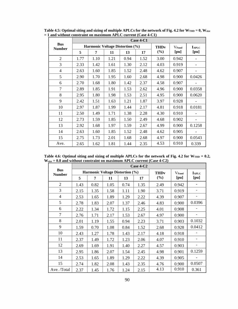
90
Table 4.5: Optimal siting and sizing of multiple APLCs for the network of Fig. 4.2 for WTHD = 0, Wsize
= 1 and without constraint on maximum APLC current (Case 4-C1)
Bus
Number
Case 4-C1
Harmonic Voltage Distortion (%) THDv
(%)
VFund
[pu]
IAPLC
[pu] 5 7 11 13 17
2 1.77 1.10 1.21 0.94 1.52 3.00 0.942 -
3 2.33 1.42 1.61 1.30 2.12 4.03 0.919 -
4 2.63 1.60 1.85 1.52 2.48 4.62 0.907 -
5 2.90 1.70 1.95 1.60 2.68 4.98 0.900 0.0426
6 2.70 1.68 1.80 1.42 2.37 4.58 0.907 -
7 2.89 1.85 1.91 1.53 2.62 4.96 0.900 0.0358
8 2.95 1.80 1.98 1.53 2.51 4.95 0.900 0.0620
9 2.42 1.51 1.63 1.21 1.87 3.97 0.928 -
10 2.97 1.87 1.99 1.44 2.17 4.81 0.918 0.0181
11 2.50 1.49 1.71 1.38 2.28 4.30 0.910 -
12 2.73 1.59 1.85 1.50 2.49 4.68 0.902 -
13 2.92 1.68 1.97 1.59 2.67 4.99 0.900 0.1258
14 2.63 1.60 1.85 1.52 2.48 4.62 0.905 -
15 2.75 1.73 2.01 1.68 2.68 4.97 0.900 0.0543
Ave.
/Total 2.65 1.62 1.81 1.44 2.35 4.53
0.910
0.339
Table 4.6: Optimal siting and sizing of multiple APLCs for the network of Fig. 4.2 for WTHD = 0.2,
Wsize = 0.8 and without constraint on maximum APLC current (Case 4-C2)
Bus
Number
Case 4-C2
Harmonic Voltage Distortion (%) THDv
(%)
VFund
[pu]
IAPLC
[pu] 5 7 11 13 17
2 1.43 0.82 1.05 0.74 1.35 2.49 0.942 -
3 2.15 1.35 1.58 1.11 1.90 3.71 0.919 -
4 2.53 1.65 1.89 1.29 2.22 4.39 0.907 -
5 2.78 1.83 2.07 1.37 2.46 4.83 0.900 0.0396
6 2.22 1.34 1.72 1.15 2.25 4.01 0.908 -
7 2.76 1.71 2.17 1.53 2.67 4.97 0.900 -
8 2.01 1.19 1.55 0.94 2.23 3.71 0.903 0.1032
9 1.59 0.70 1.08 0.84 1.52 2.68 0.928 0.0412
10 2.43 1.27 1.78 1.43 2.17 4.18 0.918 -
11 2.37 1.49 1.72 1.23 2.06 4.07 0.910 -
12 2.69 1.69 1.91 1.40 2.27 4.57 0.903 -
13 2.95 1.86 2.07 1.54 2.45 4.98 0.901 0.1259
14 2.53 1.65 1.89 1.29 2.22 4.39 0.905 -
15 2.74 1.82 2.08 1.43 2.35 4.76 0.900 0.0507
Ave. /Total 2.37 1.45 1.76 1.24 2.15 4.13
0.910
0.361
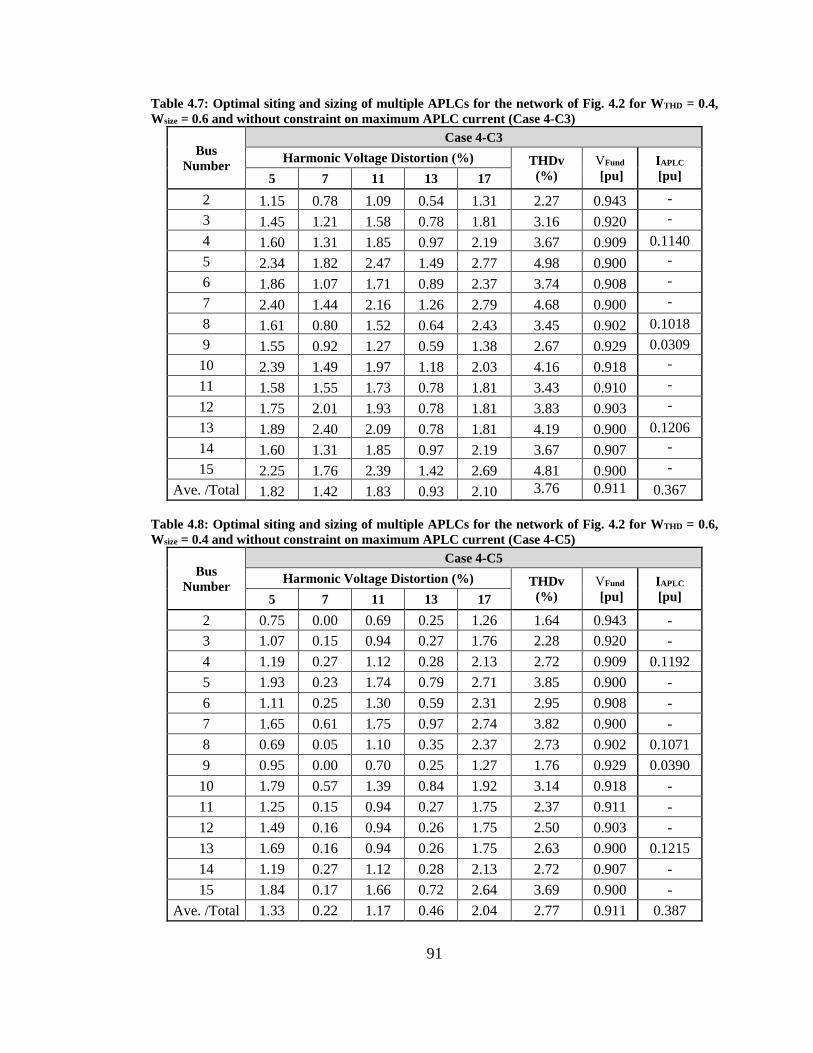
91
Table 4.7: Optimal siting and sizing of multiple APLCs for the network of Fig. 4.2 for WTHD = 0.4,
Wsize = 0.6 and without constraint on maximum APLC current (Case 4-C3)
Bus
Number
Case 4-C3
Harmonic Voltage Distortion (%) THDv
(%)
VFund
[pu]
IAPLC
[pu] 5 7 11 13 17
2 1.15 0.78 1.09 0.54 1.31 2.27 0.943 -
3 1.45 1.21 1.58 0.78 1.81 3.16 0.920 -
4 1.60 1.31 1.85 0.97 2.19 3.67 0.909 0.1140
5 2.34 1.82 2.47 1.49 2.77 4.98 0.900 -
6 1.86 1.07 1.71 0.89 2.37 3.74 0.908 -
7 2.40 1.44 2.16 1.26 2.79 4.68 0.900 -
8 1.61 0.80 1.52 0.64 2.43 3.45 0.902 0.1018
9 1.55 0.92 1.27 0.59 1.38 2.67 0.929 0.0309
10 2.39 1.49 1.97 1.18 2.03 4.16 0.918 -
11 1.58 1.55 1.73 0.78 1.81 3.43 0.910 -
12 1.75 2.01 1.93 0.78 1.81 3.83 0.903 -
13 1.89 2.40 2.09 0.78 1.81 4.19 0.900 0.1206
14 1.60 1.31 1.85 0.97 2.19 3.67 0.907 -
15 2.25 1.76 2.39 1.42 2.69 4.81 0.900 -
Ave. /Total 1.82 1.42 1.83 0.93 2.10 3.76
0.911
0.367
Table 4.8: Optimal siting and sizing of multiple APLCs for the network of Fig. 4.2 for WTHD = 0.6,
Wsize = 0.4 and without constraint on maximum APLC current (Case 4-C5)
Bus
Number
Case 4-C5
Harmonic Voltage Distortion (%) THDv
(%)
VFund
[pu]
IAPLC
[pu] 5 7 11 13 17
2 0.75 0.00 0.69 0.25 1.26 1.64 0.943 -
3 1.07 0.15 0.94 0.27 1.76 2.28 0.920 -
4 1.19 0.27 1.12 0.28 2.13 2.72 0.909 0.1192
5 1.93 0.23 1.74 0.79 2.71 3.85 0.900 -
6 1.11 0.25 1.30 0.59 2.31 2.95 0.908 -
7 1.65 0.61 1.75 0.97 2.74 3.82 0.900 -
8 0.69 0.05 1.10 0.35 2.37 2.73 0.902 0.1071
9 0.95 0.00 0.70 0.25 1.27 1.76 0.929 0.0390
10 1.79 0.57 1.39 0.84 1.92 3.14 0.918 -
11 1.25 0.15 0.94 0.27 1.75 2.37 0.911 -
12 1.49 0.16 0.94 0.26 1.75 2.50 0.903 -
13 1.69 0.16 0.94 0.26 1.75 2.63 0.900 0.1215
14 1.19 0.27 1.12 0.28 2.13 2.72 0.907 -
15 1.84 0.17 1.66 0.72 2.64 3.69 0.900 -
Ave. /Total 1.33 0.22 1.17 0.46 2.04 2.77 0.911 0.387

92
Table 4.9: Optimal siting and sizing of multiple APLCs for the network of Fig. 4.2 for WTHD = 0.8,
Wsize = 0.2 and without constraint on maximum APLC current (Case 4-C6)
Bus
Number
Case 4-C6
Harmonic Voltage Distortion (%) THDv
(%)
VFund
[pu]
IAPLC
[pu] 5 7 11 13 17
2 0.43 0.17 0.48 0.48 0.67 1.07 0.942 -
3 0.31 0.09 0.35 0.40 0.66 0.91 0.919 -
4 0.25 0.05 0.28 0.35 0.66 0.85 0.907 -
5 0.19 0.02 0.23 0.32 0.67 0.81 0.901 0.0546
6 1.35 0.60 1.45 1.28 1.63 2.93 0.908 -
7 1.88 0.96 1.90 1.66 2.05 3.88 0.900 -
8 1.20 0.40 1.43 1.26 1.63 2.81 0.903 0.1003
9 0.37 0.14 0.43 0.51 0.70 1.05 0.928 0.0470
10 1.20 0.71 1.12 1.10 1.35 2.50 0.918 -
11 0.28 0.04 0.31 0.40 0.66 0.88 0.910 -
12 0.23 0.03 0.27 0.40 0.66 0.85 0.903 -
13 0.20 0.09 0.23 0.40 0.66 0.83 0.901 0.1294
14 0.25 0.05 0.28 0.35 0.66 0.85 0.905 -
15 0.22 0.06 0.26 0.33 0.67 0.83 0.900 0.0626
Ave. /Total 0.60 0.24 0.64 0.66 0.95 1.50
0.910
0.394
Table 4.10: Optimal siting and sizing of multiple APLCs for the network of Fig. 4.2 for WTHD = 1,
Wsize = 0 and without constraint on maximum APLC current (Case 4-C7)
Bus
Number
Case 4-C7
Harmonic Voltage Distortion (%) THDv
(%)
VFund
[pu]
IAPLC
[pu] 5 7 11 13 17
2 0.01 0.01 0.00 0.00 0.01 0.13 0.942 -
3 0.01 0.01 0.00 0.01 0.01 0.13 0.919 -
4 0.01 0.01 0.00 0.01 0.02 0.13 0.907 -
5 0.02 0.01 0.01 0.01 0.02 0.13 0.900 0.0521
6 0.01 0.01 0.01 0.00 0.01 0.13 0.907 -
7 0.01 0.01 0.01 0.00 0.01 0.13 0.900 0.0487
8 0.01 0.01 0.01 0.00 0.01 0.13 0.900 0.0709
9 0.01 0.01 0.00 0.00 0.01 0.13 0.928 -
10 0.01 0.01 0.00 0.01 0.02 0.13 0.918 0.0445
11 0.01 0.01 0.01 0.01 0.01 0.09 0.910 -
12 0.01 0.01 0.01 0.01 0.02 0.09 0.902 -
13 0.02 0.01 0.01 0.01 0.02 0.09 0.900 0.1287
14 0.01 0.01 0.00 0.01 0.02 0.13 0.905 -
15 0.01 0.01 0.00 0.01 0.02 0.13 0.900 0.0614
Ave. /Total 0.01 0.01 0.01 0.01 0.01 0.12 0.910 0.0406
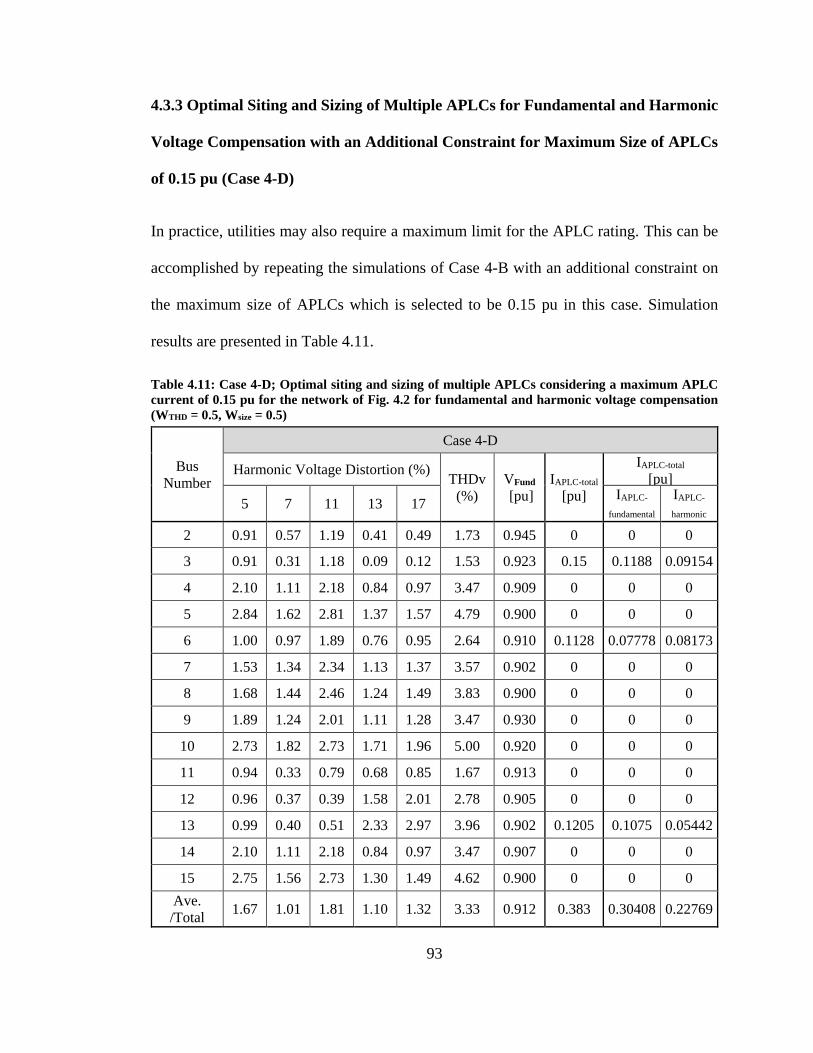
93
4.3.3 Optimal Siting and Sizing of Multiple APLCs for Fundamental and Harmonic
Voltage Compensation with an Additional Constraint for Maximum Size of APLCs
of 0.15 pu (Case 4-D)
In practice, utilities may also require a maximum limit for the APLC rating. This can be
accomplished by repeating the simulations of Case 4-B with an additional constraint on
the maximum size of APLCs which is selected to be 0.15 pu in this case. Simulation
results are presented in Table 4.11.
Table 4.11: Case 4-D; Optimal siting and sizing of multiple APLCs considering a maximum APLC
current of 0.15 pu for the network of Fig. 4.2 for fundamental and harmonic voltage compensation
(WTHD = 0.5, Wsize = 0.5)
Bus
Number
Case 4-D
Harmonic Voltage Distortion (%) THDv
(%)
VFund
[pu]
IAPLC-total
[pu]
IAPLC-total
[pu]
5 7 11 13 17 IAPLC-
fundamental
IAPLC-
harmonic
2 0.91 0.57 1.19 0.41 0.49 1.73 0.945 0 0 0
3 0.91 0.31 1.18 0.09 0.12 1.53 0.923 0.15 0.1188 0.09154
4 2.10 1.11 2.18 0.84 0.97 3.47 0.909 0 0 0
5 2.84 1.62 2.81 1.37 1.57 4.79 0.900 0 0 0
6 1.00 0.97 1.89 0.76 0.95 2.64 0.910 0.1128 0.07778 0.08173
7 1.53 1.34 2.34 1.13 1.37 3.57 0.902 0 0 0
8 1.68 1.44 2.46 1.24 1.49 3.83 0.900 0 0 0
9 1.89 1.24 2.01 1.11 1.28 3.47 0.930 0 0 0
10 2.73 1.82 2.73 1.71 1.96 5.00 0.920 0 0 0
11 0.94 0.33 0.79 0.68 0.85 1.67 0.913 0 0 0
12 0.96 0.37 0.39 1.58 2.01 2.78 0.905 0 0 0
13 0.99 0.40 0.51 2.33 2.97 3.96 0.902 0.1205 0.1075 0.05442
14 2.10 1.11 2.18 0.84 0.97 3.47 0.907 0 0 0
15 2.75 1.56 2.73 1.30 1.49 4.62 0.900 0 0 0
Ave.
/Total 1.67 1.01 1.81 1.10 1.32 3.33 0.912 0.383 0.30408 0.22769

94
Figure 4.7: Simulation results for Case 4-D (Table 4.11)
In this case, the PSO assigned 3 APLCs at buses 3, 6 and 13 with optimal sizes of 0.15
pu, 0.1128 pu and 0.1205 pu. Columns 10 and 11 in Table 4.11 are showing the
fundamental current and harmonic currents of APLCs, respectively. The total current of
APLCs (fundamental plus harmonic currents) is presented at column 9. It confirms that
each APLC is contributing in fundamental voltage compensation (StatCom application,
column 10) and harmonic voltage compensation (APF application, column 11).
It is also noticed that the calculated objective function value of this case (Eq. 4.6) is more
than case 4-B. Although, adding a constraint of the maximum size of 0.15 pu leads to the
same location of APLCs compared to case 4-B but different reference currents (APLCs
sizes) are concluded. Fig. 4.7 reveals the individual harmonic distortions and THDv
values of Case 4-D.
0
1
2
3
4
5
6
2 3 4 5 6 7 8 9 10 11 12 13 14 15
%
Bus Number
h5 h7 h11 h13 h17 THDv

95
4.3.4 Optimal Siting and Sizing of Multiple APLCs for Fundamental and Harmonic
Voltage Compensation with an Additional Constraint for Maximum Size of APLCs
of 0.10 pu (Case 4-E)
This case is identical to Case 4-D with different selected maximum size of APLCs (0.10
pu). As a result, four APLCs are located at buses 3, 6, 11 and 13 with optimal sizes of
0.100 pu, 0.100 pu, 0.098 pu and 0.087 pu, respectively. The results for this case are
presented in Table 4.12. Comparing results of Cases 4-D and 4-E, a lower limit for APLC
sizes result in more APLC units. Fig. 4.8 shows the individual harmonic distortions and
THDv of Case 4-E.
Table 4.12: Case 4-E; Optimal siting and sizing of multiple APLCs considering a maximum APLC
current of 0.10 pu for the network of Fig. 4.2 for fundamental and harmonic voltage compensation
(WTHD = 0.5, Wsize = 0.5)
Bus Number
Case 4-E
Harmonic Voltage Distortion (%) THDv
(%)
VFund
[pu]
IAPLC-total
[pu]
IAPLC-total
[pu]
5 7 11 13 17 IAPLC-
fundamental
IAPLC-
harmonic
2 1.17 0.76 0.65 1.01 0.11 1.84 0.945 0 0 0
3 0.99 0.66 0.25 1.00 0.73 1.74 0.924 0.100 0.0626 0.0780
4 2.17 1.47 1.20 1.84 0.30 3.43 0.909 0 0 0
5 2.92 1.98 1.82 2.37 0.87 4.70 0.901 0 0 0
6 1.93 1.16 1.23 1.60 0.29 3.04 0.910 0.100 0.0741 0.0671
7 2.46 1.53 1.68 1.98 0.16 3.90 0.902 0 0 0
8 2.61 1.63 1.80 2.09 0.27 4.14 0.900 0 0 0
9 2.15 1.43 1.47 1.70 0.70 3.50 0.931 0 0 0
10 2.99 2.01 2.18 2.30 1.37 4.99 0.920 0 0 0
11 0.54 0.52 0.57 0.55 1.73 2.05 0.918 0.098 0.0877 0.0439
12 1.06 1.29 0.54 0.55 2.36 2.99 0.907 0 0 0
13 1.50 1.95 0.51 0.55 2.88 3.87 0.902 0.087 0.0813 0.0314
14 2.17 1.47 1.20 1.84 0.30 3.43 0.907 0 0 0
15 2.82 1.92 1.74 2.30 0.80 4.54 0.900 0 0 0
Ave. /Total 1.96 1.41 1.20 1.55 0.92 3.44 0.913 0.385 0.3057 0.2204

96
Figure 4.8: Simulation results for Case 4-E (Table 4.12)
From economical point of view, among the three study cases of 4-B, 4-D and 4-E:
Case 4-B presents the best result with a small objective function value of 1.7625
resulting in allocations of three APLCs.
Case 4-C considers the extra constraint of maximum APLC size equal to 0.15pu and
results in the same number of APLCs as Case 4-B; however, the values of the
objective function is increased to 1.8565.
Case 4-D which is similar to Case 4-C with the maximum APLC size of 0.10pu, also
results in allocation of 4 APLCs with a slightly larger objective function value of
1.9125.
4.3.5 Optimal Online Operation of the Allocated APLCs (Case 4-F) for Fundamental
and Harmonic Voltage Compensation
For the optimal online operation of the network with APLCs (Figs. 4.2 and 4.9), the first
PSO algorithm of Fig. 4.1a is implemented to find the optimal number, locations and sizes
0
1
2
3
4
5
6
2 3 4 5 6 7 8 9 10 11 12 13 14 15
%
Bus Number
h5 h7 h11 h13 h17 THDv

97
of the required APLCs. The operation is done based on the results from case 4-D with
equal values of waiting factors (𝑊𝑠𝑖𝑧𝑒 = 𝑊𝑇𝐻𝐷 = 0.5) and maximum size of APLC of
0.15 pu. The APLCs are located on buses 3, 6 and 13 with maximum selected sizes of
0.150, 0.115 and 0.125 pu, respectively. After that, at each time step (t), SGCC receives
grid information recorded by smart meters through the SG communication network,
calculates the optimal APLC reference currents by running the second PSO algorithm
(Fig. 4.1b) and sends them to the APLCs.
Simulations are performed for different penetrations of simultaneously activated
nonlinear loads and the results are summarized in Table 4.13.
In each case (4-F1 to 4-F6), the THD and VFund with and without APLCs are presented.
For cases 4-F5 and 4-F6 the VFund is similar for with and without applying APLCs for all
buses because the VFund before applying APLCs is higher than the standard value of 0.9
pu and the APLCs not injecting any reactive power in these two cases (IAPLC-fundamental =
0). Consequently, the APLCs sizes drops dramatically from 0.132 (case 4-F4) to 0.042
(case 4-F5) pu. Figure 4.9, represent the 15-bus, 60 Hz radial network of Fig. 4.2 modeled
in Matlab/Simulink.
Figure 4.10 illustrates the voltage waveform of bus 13 (worst distorted bus of Fig. 4.9)
for with and without APLCs. It can be noticed that the blue waveform which is the voltage
of bus 13 after applying APLCs still not completely sinusoidal. The fact is that the THDv
of the network is reduced to less than 5% and not zero.

98
Table 4.13: Case 4-F; System operation with different numbers of simultaneously activated
nonlinear loads and APLCs as allocated and sized in Cases 4-D for fundamental and harmonic
voltage compensation (WTHD = 0.5, Wsize = 0.5)
Bus Number Ave./
Total 2 3 4 5 6 7 8 9 10 11 12 13 14 15
Case 4-F1: The 15-bus distorted system (Fig. 4.2) with six nonlinear loads at buses 5,7,8,10,13 and 15
Without
APLC
THD 9.69 14.34 16.69 18.19 14.67 15.74 16.03 11.58 13.21 16.17 18.77 20.99 16.69 18.00 15.77
VFund 0.925 0.891 0.877 0.869 0.883 0.875 0.873 0.911 0.901 0.874 0.854 0.842 0.875 0.868 0.880
With
APLC
THD 1.73 1.53 3.47 4.79 2.64 3.57 3.83 3.47 5.00 1.67 2.78 3.96 3.47 4.62 3.33
VFund 0.945 0.923 0.909 0.900 0.910 0.902 0.900 0.930 0.920 0.913 0.905 0.902 0.907 0.900 0.912
APLCs sizes - 0.150 - - 0.113 - - - - - - 0.121 - - 0.384
Case 4-F2: The 15-bus distorted system (Fig. 4.2) with five nonlinear loads at buses 5,7,8,10 and 15
Without
APLC
THD 8.02 11.03 13.32 14.78 12.93 13.98 14.27 9.88 11.49 11.02 11.01 11.01 13.32 14.59 12.19
VFund 0.932 0.904 0.890 0.881 0.889 0.882 0.880 0.918 0.908 0.896 0.890 0.889 0.888 0.881 0.895
With
APLC
THD 1.71 1.38 3.45 4.80 2.60 3.53 3.79 3.47 5.00 0.85 1.22 2.05 3.45 4.63 2.99
VFund 0.945 0.924 0.909 0.900 0.910 0.902 0.900 0.931 0.920 0.915 0.909 0.908 0.907 0.900 9.13
APLCs sizes - 0.150 - - 0.105 - - - - - - 0.017 - - 0.272
Case 4-F3: The 15-bus distorted system (Fig. 4.2) with four nonlinear loads at buses 8,10,13 and 15
Without
APLC
THD 6.53 9.61 10.79 10.79 9.02 9.02 10.29 8.36 9.94 11.36 13.84 15.97 10.79 12.02 10.60
VFund 0.939 0.910 0.900 0.899 0.909 0.907 0.899 0.924 0.914 0.892 0.872 0.860 0.898 0.891 0.901
With
APLC
THD 1.86 1.98 2.71 2.71 2.87 2.87 4.00 3.50 5.00 2.12 2.78 3.55 2.71 3.69 3.02
VFund 0.945 0.923 0.912 0.911 0.915 0.913 0.905 0.931 0.921 0.912 0.903 0.900 0.910 0.903 9.15
APLCs sizes - 0.038 - - 0.028 - - - - - - 0.124 - - 0.19
Case 4-F4: The 15-bus distorted system (Fig. 4.2) with three nonlinear loads at buses 5,7 and 13.
Without
APLC
THD 4.57 7.45 8.49 9.87 6.76 7.74 6.76 4.57 4.57 9.16 11.59 13.68 8.49 8.49 8.01
VFund 0.947 0.919 0.909 0.900 0.918 0.910 0.916 0.944 0.943 0.901 0.881 0.868 0.907 0.907 0.912
With
APLC
THD 2.04 2.68 3.66 4.98 4.03 4.99 4.03 2.04 2.04 3.19 3.91 4.52 3.66 3.66 3.53
VFund 0.952 0.929 0.919 0.910 0.924 0.916 0.921 0.949 0.948 0.917 0.905 0.900 0.917 0.917 0.923
APLCs sizes - 0.037 - - 0.006 - - - - - - 0.089 - - 0.132
Case 4-F5: The 15-bus distorted system (Fig. 4.2) with two nonlinear loads at buses 10 and 15
Without
APLC
THD 3.20 4.72 5.86 5.86 3.20 3.20 3.20 4.98 6.52 4.72 4.71 4.71 5.86 7.04 4.84
VFund 0.953 0.931 0.920 0.919 0.938 0.936 0.935 0.939 0.928 0.923 0.916 0.915 0.918 0.911 0.927
With
APLC
THD 1.81 2.22 3.18 3.18 1.80 1.80 1.80 3.50 5.00 2.22 2.22 2.22 3.18 4.26 2.74
VFund 0.953 0.931 0.920 0.919 0.938 0.936 0.935 0.939 0.928 0.923 0.916 0.915 0.918 0.911 0.927
APLCs sizes - 0.042 - - 0 - - - - - - 0 - - 0.042
Case 4-F6: The 15-bus distorted system (Fig. 4.2) with one nonlinear load at bus 5
Without
APLC
THD 1.47 2.82 3.83 5.16 1.46 1.46 1.46 1.47 1.47 2.81 2.81 2.81 3.83 3.83 2.62
VFund 0.961 0.939 0.929 0.920 0.946 0.944 0.943 0.958 0.957 0.931 0.924 0.923 0.927 0.927 0.938
With
APLC
THD 1.39 2.66 3.67 5.00 1.38 1.38 1.38 1.39 1.39 2.66 2.66 2.66 3.67 3.67 2.50
VFund 0.961 0.939 0.929 0.920 0.946 0.944 0.943 0.958 0.957 0.931 0.924 0.923 0.927 0.927 0.938
APLCs sizes - 0.003 - - 0 - - - - - - 0 - - 0.003

99
Figure 4.9: Line diagram of the three-phase 15-bus distorted system [139] in Matlab/Simulink
with six nonlinear loads (Tables 3.1 and 3.2)
0.02 0.03 0.04 0.05 0.06 0.07
With APLC
Without APLC
0.2
0
-0.2
-0.4
-0.6
-0.8
0.4
0.6
0.8
Time [s]
Vo
lta
ge o
f B
us
13
[p
u]
Figure 4.10: Voltage waveform of bus 13 before (red line) and after (blue line) operation of APLCs

100
Bus 2 Bus 3 Bus 4&14 Bus 5 Bus 6 Bus 7 Bus 8 Bus 9 Bus 10 Bus 11 Bus 12 Bus 13 Bus 15
0.02 0.03 0.04 0.05 0.06 0.07 0.08 0.09 0.10 0.11 0.12 0.13 0.14 0.15
4
5
6
8
10
12
2
TH
Dv [
%]
Case 4-F1 (6 nonlinear loads and 3 APLCs)
Transient due to APLC operation
Case 4-A (6 nonlinearloads with no APLC)
Case 4-F2 (5 nonlinear loads and 3 APLCs)
Case 4-F3 (4 nonlinear loads and 3 APLCs)
Case 4-F4(3nonlinear loads and 3 APLCs)
14
16
18
20
22
0
Time [s] Figure 4.11: The THDv profiles of all buses for the optimal online operation of the 15-bus network
of Fig. 4.2 for Cases 4-F4 to 4-F1
Bus 2 Bus 3 Bus 4 Bus 5 Bus 6 Bus 7 Bus 8 Bus 9 Bus 10 Bus 11 Bus 12 Bus 13 Bus 14 Bus 15
0.02 0.03 0.04 0.05 0.06 0.07 0.08 0.09 0.10 0.11 0.12 0.13 0.14 0.15
0.84
0.86
0.88
0.90
0.92
0.94
0.96
Fu
nd
am
en
tal
RM
S V
olt
ag
e o
f B
use
s [p
u]
Time [s]
Case 4-F1 (6 nonlinearloads and 3 APLCs)
Case 4-A (6 nonlinearloads with no APLC)
Case 4-F2 (5 nonlinearloads and 3 APLCs)
Case 4-F3 (4 nonlinearloads and 3 APLCs)
Case 4-F4(3nonlinear loads and 3 APLCs)
Figure 4.12: The VFund profiles of all buses for the optimal online operation of the 15-bus network
of Fig. 4.2 for Cases 4-F4 to 4-F1
Figs. 4.11-4.13 demonstrate the online optimal operation of 15-bus network with the
three APLCs installed at optimal locations and ratings determined in Case 4-D. The
number of nonlinear loads is gradually changed from 3 to 6 units (Cases 4-F4 to 4-
F1). Fig. 4.11 shows the THDv of all buses of Fig. 4.9. Based on this figure, the THDv
of bus 13 before applying APLCs is 20.99% which this value after implementing
APLCs is 3.96%, 2.55%, 3.55 and 4.52% for Cases 4-F1, 4-F2, 4-F3 and 4-F4,
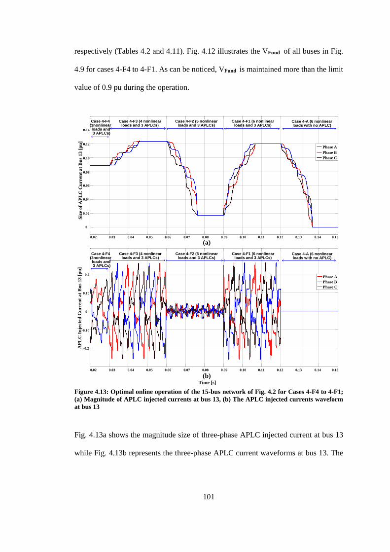
101
respectively (Tables 4.2 and 4.11). Fig. 4.12 illustrates the VFund of all buses in Fig.
4.9 for cases 4-F4 to 4-F1. As can be noticed, VFund is maintained more than the limit
value of 0.9 pu during the operation.
Time [s]
Siz
e o
f A
PL
C C
urren
t a
t B
us
13 [
pu
]
Phase A
Phase B
Phase C
0.02 0.03 0.04 0.05 0.06 0.07 0.08 0.09 0.10 0.11 0.12 0.13 0.14 0.15
-0.2
-0.10
0
0.10
AP
LC
In
jecte
d C
urre
nt
at
Bu
s 1
3 [
pu
]
0.2
Phase A
Phase B
Phase C
0.02 0.03 0.04 0.05 0.06 0.07 0.08 0.09 0.10 0.11 0.12 0.13 0.14 0.15
0
0.02
0.04
0.06
0.08
0.10
0.12
0.14
(a)
(b)
Case 4-F1 (6 nonlinearloads and 3 APLCs)
Case 4-A (6 nonlinearloads with no APLC)
Case 4-F2 (5 nonlinearloads and 3 APLCs)
Case 4-F3 (4 nonlinearloads and 3 APLCs)
Case 4-F4(3nonlinear loads and 3 APLCs)
Case 4-F1 (6 nonlinearloads and 3 APLCs)
Case 4-A (6 nonlinearloads with no APLC)
Case 4-F2 (5 nonlinearloads and 3 APLCs)
Case 4-F3 (4 nonlinearloads and 3 APLCs)
Case 4-F4(3nonlinear loads and 3 APLCs)
Figure 4.13: Optimal online operation of the 15-bus network of Fig. 4.2 for Cases 4-F4 to 4-F1;
(a) Magnitude of APLC injected currents at bus 13, (b) The APLC injected currents waveform
at bus 13
Fig. 4.13a shows the magnitude size of three-phase APLC injected current at bus 13
while Fig. 4.13b represents the three-phase APLC current waveforms at bus 13. The

102
magnitude of APLC current at bus 13 is 0.089 pu, 0.124 pu, 0.017 pu, 0.121 pu and
zero for cases 4-F4, 4-F3, 4F2, 4F1 and 4-A, respectively.
Simulations are initially started with three nonlinear loads (at buses 5, 7 and 13) with
three APLCs at buses 3, 6 and 13 (see Fig. 4.9) followed by four switching actions: i)
at t=0.03sec, nonlinear loads at buses 5 and 7 are switched off and nonlinear loads at
bus 8, 10 and 15 are switched on, ii) at t=0.06sec, nonlinear loads at buses 5 and 7 are
switched back in operation and nonlinear load at bus 13 is switched off while nonlinear
loads at buses 8, 10 and 15 are still in operation, iii) at t=0.09sec, the only nonlinear
load at bus 13 which was switched off is switch back again and all nonlinear loads are
in operation, and iv) at t=0.12sec, all APLCs are switched off while all nonlinear loads
are still in operation.
Note that:
The transient network conditions are due to the switching actions and changes in the
number of nonlinear loads.
Without APLCs in operation (t>0.12sec), the THDv and VFund of all buses are
above the recommended value of 5% and below 0.9 pu, respectively, while during
the operation of APLCs, the steady-state values of THDv at all buses for all cases
are less than 5% and VFund at all buses are more than 0.9 pu.
At t=0.06sec (Case 4-F2), just nonlinear load at bus 13 is switched off. Therefore
as confirmed by Table 4.13 and Figs. 13a and 13b, the injected current of APLC at
bus 13 is reduced.

103
CHAPTER 5: IMPACTS OF HARMONIC COUPLINGS ON
OPTIMAL SITING, SIZING AND ONLINE CONTROL OF
MULTIPLE APLCS
In the literature, the effects of harmonic couplings are neglected in the optimal design
and operation of APLCs since they are commonly modeled as decoupled harmonic
current sources injecting harmonic currents at PCCs.
5.1 Nonlinear Modeling and Control of APLCs
To properly include the impacts of harmonic couplings, a detailed nonlinear model is
used for the APLCs and their performances are considered under different conditions.
The APLC inverters are designed with the five level neutral-point clamped (FL-NPC)
configuration (section 3.2.4, Eqs. 3.14-3.19).
This chapter implements a PSO-based algorithm for optimal siting and sizing of
multiple APLCs where the impacts of harmonic couplings are considered by using
nonlinear models for APLCs and nonlinear loads in Matlab/Simulink. The size of an
APLC is calculated based on:
HhKkIIH
h
hAPLCksizeAPLCk ...,,2,...,,1,
2
2
,,
(5.1)
where k and h are the bus number and the harmonic order while K and H represent
their maximum values, respectively.
The objective function for optimal siting and sizing of APLCs is to minimize the total
cost associated with their sizes and the overall network THDv:
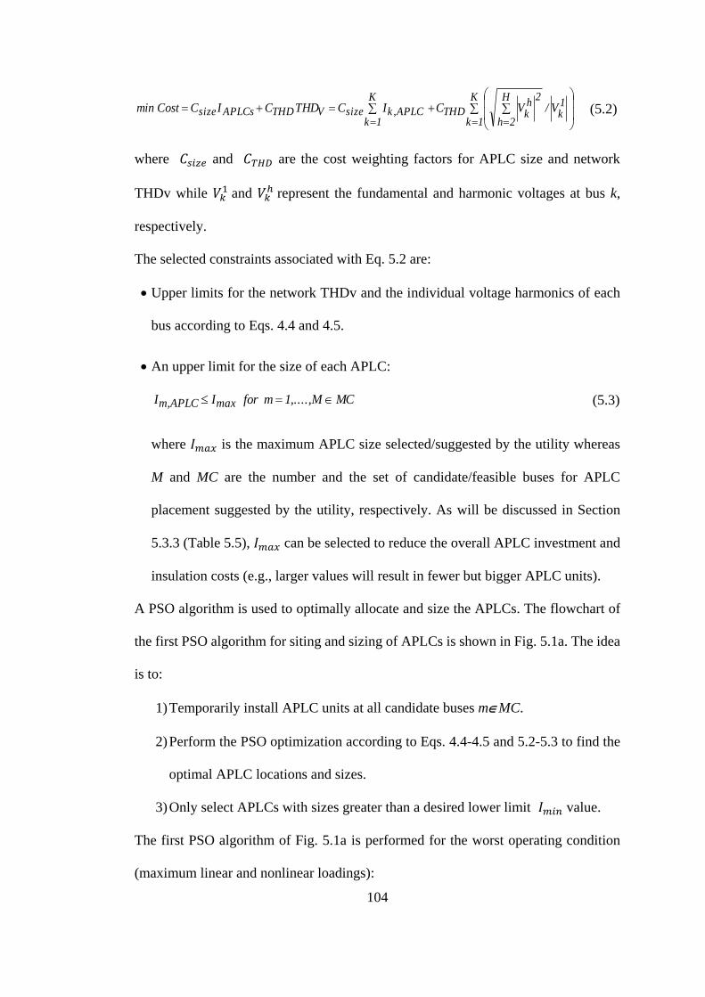
104
K
1k
1k
H
2h
2hkTHD
K
1kAPLC,ksizeVTHDAPLCssize V/VCICTHDCICCostmin (5.2)
where 𝐶𝑠𝑖𝑧𝑒 and 𝐶𝑇𝐻𝐷 are the cost weighting factors for APLC size and network
THDv while 𝑉𝑘1 and 𝑉𝑘
ℎ represent the fundamental and harmonic voltages at bus k,
respectively.
The selected constraints associated with Eq. 5.2 are:
Upper limits for the network THDv and the individual voltage harmonics of each
bus according to Eqs. 4.4 and 4.5.
An upper limit for the size of each APLC:
MCM....,,1mforII maxAPLC,m (5.3)
where 𝐼𝑚𝑎𝑥 is the maximum APLC size selected/suggested by the utility whereas
M and MC are the number and the set of candidate/feasible buses for APLC
placement suggested by the utility, respectively. As will be discussed in Section
5.3.3 (Table 5.5), 𝐼𝑚𝑎𝑥 can be selected to reduce the overall APLC investment and
insulation costs (e.g., larger values will result in fewer but bigger APLC units).
A PSO algorithm is used to optimally allocate and size the APLCs. The flowchart of
the first PSO algorithm for siting and sizing of APLCs is shown in Fig. 5.1a. The idea
is to:
1) Temporarily install APLC units at all candidate buses mMC.
2) Perform the PSO optimization according to Eqs. 4.4-4.5 and 5.2-5.3 to find the
optimal APLC locations and sizes.
3) Only select APLCs with sizes greater than a desired lower limit 𝐼𝑚𝑖𝑛 value.
The first PSO algorithm of Fig. 5.1a is performed for the worst operating condition
(maximum linear and nonlinear loadings):
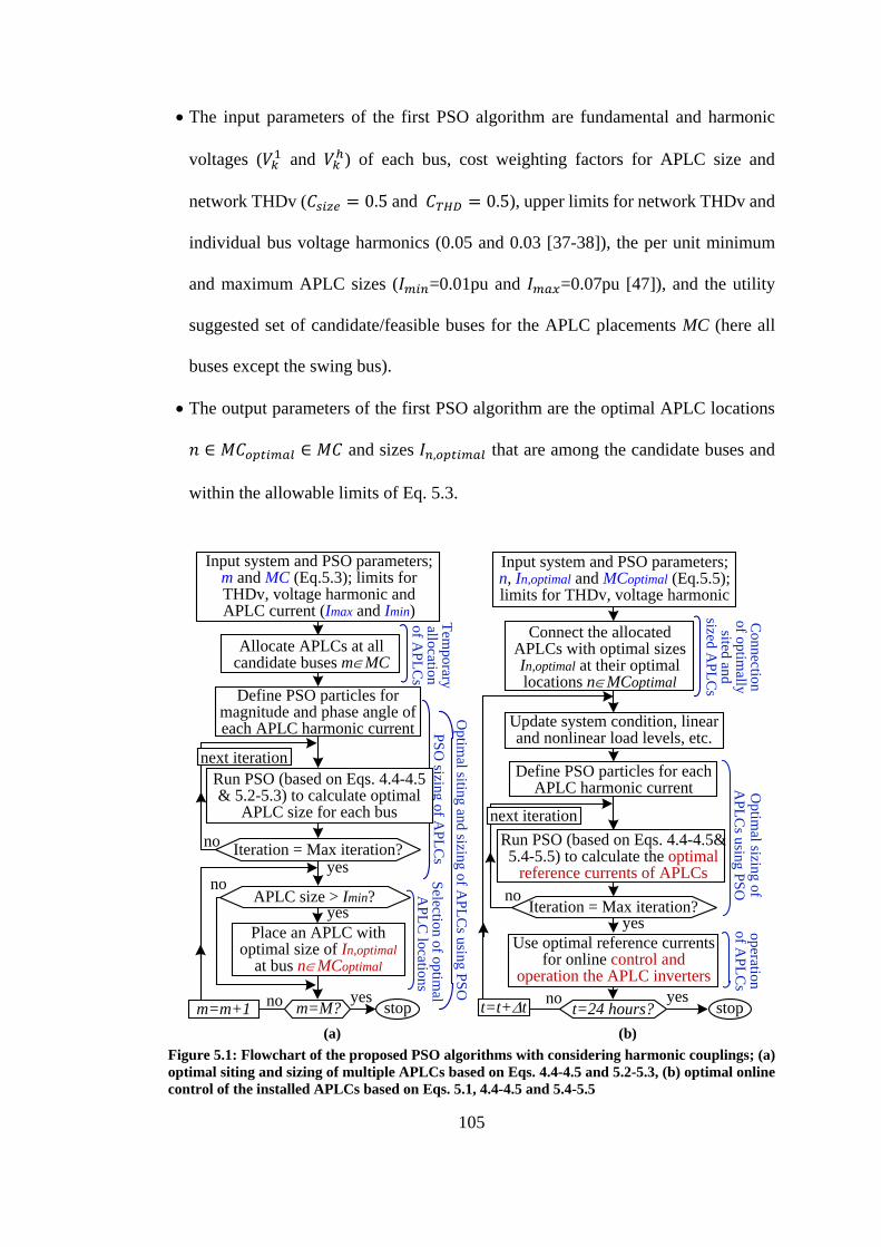
105
The input parameters of the first PSO algorithm are fundamental and harmonic
voltages (𝑉𝑘1 and 𝑉𝑘
ℎ) of each bus, cost weighting factors for APLC size and
network THDv (𝐶𝑠𝑖𝑧𝑒 = 0.5 and 𝐶𝑇𝐻𝐷 = 0.5), upper limits for network THDv and
individual bus voltage harmonics (0.05 and 0.03 [37-38]), the per unit minimum
and maximum APLC sizes (𝐼𝑚𝑖𝑛=0.01pu and 𝐼𝑚𝑎𝑥=0.07pu [47]), and the utility
suggested set of candidate/feasible buses for the APLC placements MC (here all
buses except the swing bus).
The output parameters of the first PSO algorithm are the optimal APLC locations
𝑛 ∈ 𝑀𝐶𝑜𝑝𝑡𝑖𝑚𝑎𝑙 ∈ 𝑀𝐶 and sizes 𝐼𝑛,𝑜𝑝𝑡𝑖𝑚𝑎𝑙 that are among the candidate buses and
within the allowable limits of Eq. 5.3.
Op
timal sitin
g an
d sizin
g o
f AP
LC
s usin
g P
SO
PS
O sizin
g o
f AP
LC
sT
emp
orary
allo
cation
o
f AP
LC
s
Selectio
n o
f op
timal
AP
LC
locatio
ns
Place an APLC with optimal size of In,optimal
at bus nMCoptimal
stopm=m+1
Define PSO particles for magnitude and phase angle of each APLC harmonic current
yes
no
yesno
yes
noIteration = Max iteration?
Run PSO (based on Eqs. 4.4-4.5 & 5.2-5.3) to calculate optimal
APLC size for each bus
APLC size > Imin?
m=M?
Allocate APLCs at all candidate buses mMC
Input system and PSO parameters; m and MC (Eq.5.3); limits for THDv, voltage harmonic and APLC current (Imax and Imin)
next iteration
Co
nn
ection
o
f op
timally
sited
and
sized
AP
LC
s
op
eration
o
f AP
LC
sO
ptim
al sizing
of
AP
LC
s usin
g P
SO
Use optimal reference currents for online control and
operation the APLC inverters
stop
Define PSO particles for each APLC harmonic current
yesno
yes
noIteration = Max iteration?
Run PSO (based on Eqs. 4.4-4.5& 5.4-5.5) to calculate the optimal
reference currents of APLCs
t=24 hours?
Connect the allocated APLCs with optimal sizes In,optimal at their optimal locations nMCoptimal
Update system condition, linear and nonlinear load levels, etc.
t=t+t
next iteration
Input system and PSO parameters; n, In,optimal and MCoptimal (Eq.5.5); limits for THDv, voltage harmonic
(a) (b)
Figure 5.1: Flowchart of the proposed PSO algorithms with considering harmonic couplings; (a)
optimal siting and sizing of multiple APLCs based on Eqs. 4.4-4.5 and 5.2-5.3, (b) optimal online
control of the installed APLCs based on Eqs. 5.1, 4.4-4.5 and 5.4-5.5

106
5.2 Optimal Online Operation of APLCs Considering Harmonic Couplings
The second PSO algorithm (Fig. 5.1b) for online control of the 𝑛 allocated APLCs
(𝐼𝑛,𝑜𝑝𝑡𝑖𝑚𝑎𝑙; 𝑛 ∈ 𝑀𝐶𝑜𝑝𝑡𝑖𝑚𝑎𝑙) is based on the online bus data information received from
the smart meters through the SG communication infrastructure. The problem
formulation is similar to Eqs. 4.4-4.5 and 5.2-5.3 with the following differences:
APLCs are only installed at optimal locations (𝑀𝐶𝑜𝑝𝑡𝑖𝑚𝑎𝑙) with optimal sizes
(𝐼𝑛,𝑜𝑝𝑡𝑖𝑚𝑎𝑙) as determined by the first PSO algorithm of Fig. 5.1a.
Network status and optimization of the objective function (Eq. 5.4) are updated at
time steps of ∆𝑡 for the period of 24 hours:
...,t2,tfor)t(V/)t(V)t(THDminK
1k
1k
H
2h
2hkv
(5.4)
The bus numbers and limits of Eq. 5.3 are modified as follows:
optimaloptimalnAPLCn MCnforII ,, (5.5)
where 𝐼𝑛,𝑜𝑝𝑡𝑖𝑚𝑎𝑙 and 𝑀𝐶𝑜𝑝𝑡𝑖𝑚𝑎𝑙are the optimal sizes and locations of APLCs as
determined by the first PSO algorithm (Fig. 5.1a).
The flowchart of the second PSO algorithm for optimal operation/control of the
allocated APLCs is shown in Fig. 5.1b:
The input parameters of the second PSO algorithm are the same as those for the
first PSO algorithm (Fig. 5.1a) with the exceptions of: i) the bus fundamental and
harmonic voltages (𝑉𝑘1 and 𝑉𝑘
ℎ) are transmitted online by the smart meters and
updated at each time step ∆𝑡, ii) the maximum APLC sizes are the ratings of the
selected APLCs ( 𝐼𝑛,𝑚𝑎𝑥 = 𝐼𝑛,𝑜𝑝𝑡𝑖𝑚𝑎𝑙), iii) the candidate buses are 𝑀𝐶𝑜𝑝𝑡𝑖𝑚𝑎𝑙.
The output parameters of the second PSO algorithm are the optimal APLC

107
reference currents at time steps of ∆𝑡 for the period of 24 hours such that the overall
network THDv and the individual bus voltage harmonics are within the limits of
IEEE-519 standard [37-38].
5.3 Simulations for Optimal Siting/Sizing of APLCs with Considering Harmonic
Couplings
The simulated network in this chapter is the same as chapter 4 (the 15-bus, 60Hz radial
network, Fig 4.2). However, the nonlinear loads are the actual Matlab/Simulink model
including three-phase full bridge rectifiers with resistive loads (Table 5.1) connected
to buses 5, 7, 8, 10, 13, and 15. The optimal siting and sizing simulations are performed
for the worse scenario with maximum linear and non-linear loading conditions.
Table 5.1: Current harmonic injection of the nonlinear loads (in percentage of the fundamental
component) in the network of Fig.4.2
*) Exact nonlinear model is adopted from Matlab/Simulink library.
**) Conventional modeling approach adopted in most APLC related publications [37-48].
In this chapter, six study cases (Table 5.2) are simulated and the results are presented
in Tables 5.3-5.7. In each case except Case 3, simulations are performed and compared
with and without harmonic couplings.
Harmonic Order
5 7 11 13 17
The Exact Nonlinear Model with Harmonic Couplings*
Exact Calculation Exact Calculation Exact Calculation Exact Calculation Exact Calculation The exact nonlinear load models and their harmonic injections are adopted from the Matlab/Simulink
library. Therefore, the injected current harmonics (magnitudes and phase angles) depend on the
nonlinear load characteristics, inherent couplings among harmonics, (non)sinusoidal terminal voltage,
and system operating conditions.
The Approximate Decoupled Model without Harmonic Couplings**
22.60 11.34 9.02 6.49 5.63
Each nonlinear load is modeled with decupled harmonic current sources injecting harmonic currents
that are equal (in magnitude and phase angle) to the current distortions of the exact model with rated
sinusoidal voltage excitation. Therefore, the injected current harmonics are fixed and independent of
system operating conditions.

108
Table 5.2: Simulated case studies for the distorted 15-bus network of Fig.4.2 with considering
harmonic couplings
Case System Description Approach Results
5-A System operation without APLCs - Table 5.3
5-B Optimal APLC siting/sizing not considering Imax (Eq. 5.3) First PSO of Fig. 5.1a Table 5.4
5-C Impact of Imax (Eq. 5.3) on the APLC siting/sizing solution First PSO of Fig. 5.1a Table 5.5
5-D Optimal APLC siting/sizing with Imax=0.07pu (Eq. 5.3). First PSO of Fig. 5.1a Table 5.6
5-E System operation with four optimally located/sized APLCs of Case 5-
D Second PSO of Fig. 5.1b Table 5.7
5-F Online operation/control of APLCs under different operating
conditions Second PSO of Fig. 5.1b Fig. 5.6
5.3.1 Case 5-A: System Operation without APLCs
This case illustrates the worse operating condition of the network with maximum
loadings of all linear and nonlinear loads. Simulation results with and without
harmonic couplings (Cases 5-A1 and 5-A2) are presented in Table 5.3 and Fig. 5.2
showing individual voltage harmonics (columns 2-6 and 8-12) and THDv of all buses
(columns 7 and 13). Clearly, the entire network is highly distorted, the THDv of all
buses are higher than the permitted limit of 5% and the voltage harmonics of most
buses are above the acceptable level of 3%. Bus 13 is the worst distorted point of the
network due to its remote location from bus 1 (the swing bus). Note that simulation
results of Case 5-A2 are very different from the accurate results of Case 5-A1;
therefore, disregarding harmonic couplings as adopted in most APLC related
publications [40-51] may result in significant errors. For example, the worst bus THDv
(Table 5.3, bus 13) and the network THDv (last row) are increased from 13.37% and
10.09% (Case 5-A1) to 20.99% and 15.77% (Case 5-A2) indicating errors of 56% and
57%, respectively (Fig 5.2c).

109
Table 5.3: Case 5-A; Operation of the network in Fig.4.2 without any APLCs
Bus
Case 5-A1: Considering Harmonic
Couplings
(Table 2, rows 3-5)
Case 5-A2: Not Considering Harmonic
Couplings
(Table 2, rows 6-8)
Harmonic Voltage Distortion
(%) THDv
(%)
Harmonic Voltage Distortion (%) THDv
(%) 5 7 11 13 17 5 7 11 13 17
2 4.78 2.53 2.14 1.42 0.66 6.08 5.35 3.70 4.50 3.77 4.13 9.69
3 7.10 3.71 3.16 2.02 1.19 9.06 7.94 5.48 6.66 5.58 6.11 14.34
4 8.29 4.35 3.75 2.40 1.49 10.69 9.23 6.38 7.75 6.49 7.10 16.69
5 9.06 4.75 4.13 2.63 1.71 11.77 10.07 6.95 8.44 7.07 7.74 18.19
6 7.32 3.91 3.38 2.28 1.18 9.47 8.13 5.60 6.80 5.70 6.26 14.67
7 7.87 4.20 3.64 2.48 1.27 10.19 8.72 6.00 7.30 6.11 6.71 15.74
8 8.02 4.28 3.72 2.51 1.35 10.44 8.88 6.12 7.43 6.23 6.84 16.03
9 5.75 3.08 2.59 1.81 0.67 7.35 6.40 4.42 5.37 4.50 4.94 11.58
10 6.60 3.56 3.01 2.16 0.80 8.52 7.31 5.04 6.13 5.14 5.64 13.21
11 7.98 4.13 3.49 2.16 1.41 10.18 8.96 6.18 7.50 6.28 6.87 16.17
12 9.25 4.74 4.00 2.39 1.80 11.87 10.42 7.17 8.71 7.29 7.97 18.77
13 10.34 5.26 4.44 2.59 2.15 13.37 11.66 8.02 9.73 8.15 8.91 20.99
14 8.29 4.35 3.75 2.40 1.49 10.69 9.23 6.38 7.75 6.49 7.10 16.69
15 8.97 4.70 4.07 2.61 1.63 11.58 9.96 6.88 8.35 7.00 7.66 18.00
Avg. 7.83 4.11 3.52 2.28 1.34 10.09* 8.73 6.02 7.32 6.13 6.71 15.77*
*) Network Average THDv.
(a)
0
2
4
6
8
10
12
14
16
2 3 4 5 6 7 8 9 10 11 12 13 14 15
%
Bus Number
h5 h7 h11 h13 h17 THDv

110
(b)
(c)
Figure 5.2: Simulation results for Case 5-A; (a) Case 5-A1, (b) Case 5-A2, (c) comparing THDv
of all buses for Cases 5-A1and 5-A2
5.3.2 Case 5-B: Optimal Siting and Sizing of Multiple APLCs without
Considering the Maximum APLC Size
The PSO algorithm of Fig. 5.1a is used (without considering Imax in Eq. 5.3) to find
the optimal locations and sizes of the APLCs for the 15-bus network of Fig. 4.2.
Simulation results are summarized in Table 5.4 for Cases 5-B1 and 5-B2 in columns
2-8 and 9-15, respectively and Fig 5.3. Both cases use the first PSO algorithm of Fig.
5.1a. However, decoupled harmonic current sources are used for the nonlinear load
modeling in Case 5-B2.
02468
1012141618202224
2 3 4 5 6 7 8 9 10 11 12 13 14 15
TH
Dv
%
Bus Number
h5 h7 h11 h13 h17 THDv
0
5
10
15
20
25
2 3 4 5 6 7 8 9 10 11 12 13 14 15 Ave.
TH
Dv
%
Bus Number
Case 5-A1 Case 5-A2

111
Table 5.4: Case 5-B; Optimal siting and sizing of multiple APLCs (the first PSO algorithm of Fig.
5.1a and not considering a maximum APLC size)
Bus
Case 5-B1: Considering Harmonic
Couplings (Table 5.1, rows 3-5)
Case 5-B2: Not Considering Harmonic
Couplings (Table 5.1, rows 6-8)
Harmonic Voltage
Distortion (%) THDv
(%)
Allocated
IAPLC
(pu)
Harmonic Voltage
Distortion (%) THDv
(%)
Allocated
IAPLC (pu) 5 7 11 13 17 5 7 11 13 17
2 0.29 0.66 0.70 0.61 0.46 2.13 0 0.67 0.52 1.03 0.46 0.82 1.64 0
3 1.22 1.74 1.71 1.79 0.89 4.15 0.205 0.09 0.15 0.87 0.14 0.25 0.94 0
4 0.09 1.23 0.82 1.11 0.40 3.45 0 1.16 0.99 1.90 0.79 1.09 2.79 0
5 0.78 1.09 0.37 0.72 0.71 3.73 0 1.93 1.52 2.55 1.34 1.70 4.15 0
6 1.70 1.52 1.66 1.02 0.73 4.12 0.040 1.52 1.01 1.76 1.08 2.11 3.47 0.062
7 2.21 1.83 1.83 1.14 0.86 4.71 0 2.07 1.39 2.22 1.47 2.56 4.46 0
8 2.36 1.92 1.94 1.23 0.93 5.00 0 2.22 1.49 2.35 1.58 2.68 4.73 0
9 1.24 0.99 0.87 0.55 0.77 3.09 0 1.66 1.21 1.87 1.17 1.62 3.43 0
10 2.08 1.41 1.32 0.78 1.16 4.30 0 2.52 1.80 2.60 1.79 2.31 4.99 0
11 0.37 1.55 1.31 1.48 0.81 3.77 0 2.75 1.59 1.02 2.08 2.29 4.55 0.173
12 1.05 1.48 1.02 1.08 0.95 4.07 0 1.47 0.70 0.33 1.16 1.26 2.39 0
13 2.14 1.66 1.21 0.85 1.25 4.98 0 0.39 0.06 1.11 0.38 0.38 1.29 0
14 0.09 1.23 0.82 1.11 0.40 3.44 0 1.16 0.99 1.90 0.79 1.09 2.79 0
15 0.69 1.06 0.36 0.75 0.64 3.56 0 1.83 1.45 2.47 1.27 1.62 3.97 0
Avg. 1.16 1.38 1.14 1.01 0.78 3.89* 0.245** 1.53 1.06 1.71 1.11 1.56 3.26* 0.235**
*) Network Average THDv
**) Total size of allocated APLCs
Note that the accurate solution of Case 5-B1 that includes harmonic couplings requires
two APLCs at buses 3 and 6 (Table 5.4: column 8, rows 5 and 8) with ratings of
0.205pu and 0.040pu, respectively. However, the approximate modeling of Case 5-B2
indicates different locations (buses 6 and 11) and sizes (0.062pu and 0.173pu) of
APLCs (Table 5.4: last column, rows 8 and 13).
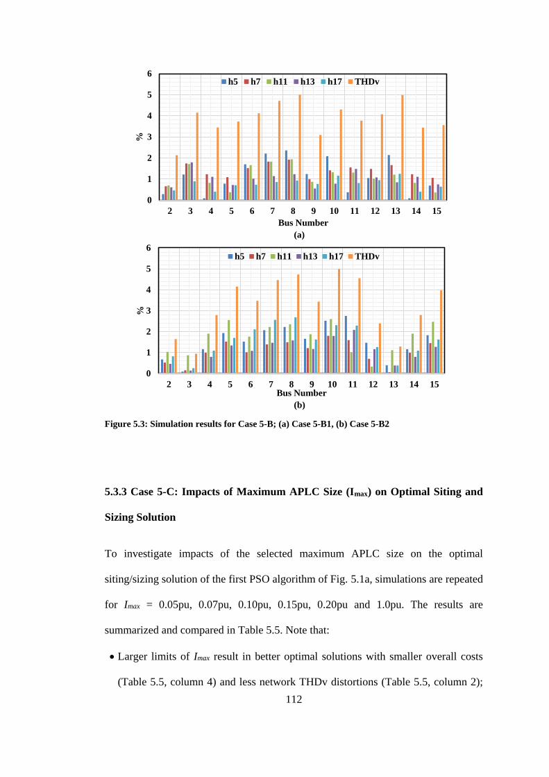
112
(a)
(b)
Figure 5.3: Simulation results for Case 5-B; (a) Case 5-B1, (b) Case 5-B2
5.3.3 Case 5-C: Impacts of Maximum APLC Size (Imax) on Optimal Siting and
Sizing Solution
To investigate impacts of the selected maximum APLC size on the optimal
siting/sizing solution of the first PSO algorithm of Fig. 5.1a, simulations are repeated
for Imax = 0.05pu, 0.07pu, 0.10pu, 0.15pu, 0.20pu and 1.0pu. The results are
summarized and compared in Table 5.5. Note that:
Larger limits of Imax result in better optimal solutions with smaller overall costs
(Table 5.5, column 4) and less network THDv distortions (Table 5.5, column 2);
0
1
2
3
4
5
6
2 3 4 5 6 7 8 9 10 11 12 13 14 15
%
Bus Number
h5 h7 h11 h13 h17 THDv
0
1
2
3
4
5
6
2 3 4 5 6 7 8 9 10 11 12 13 14 15
%
Bus Number
h5 h7 h11 h13 h17 THDv

113
however, the total size of the APLCs increases (Table 5.5, column 3). Furthermore,
fewer (but larger) APLC units are allocated that may also reduce the APLC
investment and maintenance costs for the electric utilities.
On the other hand, smaller limits of Imax reduce the total APLC size (Table 5.5,
column 3); however, the THDv and overall cost (Table 5.5, column 2 and 4) as well
as the number of APLC units will increase. Furthermore, it is unlikely to install
more than a few APLCs in practical applications.
From technical and practical points of view, it is better to select larger limits for
Imax. This will result in lower costs with better voltage qualities, fewer APLC units
and less maintenance and investment costs. A possible limitation may occur on the
availability of large APLC units.
In this chapter, the compromised value of Imax=0.07pu [47] is selected and used.
Table 5.5: Case 5-C; Impact of maximum APLC size on the optimal siting and sizing solution
𝑰𝒎𝒂𝒙
(Eq. 5.3)
[pu]
Solutions of the first PSO Algorithm (Fig. 5.1a) including harmonic couplings
(Table 5.1, rows 3-5)
Cost Function (Eq. 5.2) Optimal APLC Locations/Sizes
𝑻𝑯𝑫𝑵𝒆𝒕 𝑰𝑨𝑷𝑳𝑪 min
Cost APLC 1 APLC 2 APLC 3 APLC 4 APLC 5
APLC
6
1.00 3.88 0.245 2.062 Bus 3/
0.205pu
Bus 6
/0.040pu
0.30 3.88 0.245 2.062 Bus 3
/0.205pu
Bus 6
/0.040pu
0.20 3.86 0.266 2.063 Bus 3
/0.200pu
Bus 6
/0.066pu
0.15 4.07 0.234 2.152 Bus 3
/0.140pu
Bus 6
/0.054pu
Bus 12
/0.040pu
0.10 4.10 0.214 2.157 Bus 3
/0.100pu
Bus 6
/0.060pu
Bus 12
/0.054pu
0.07* 4.16 0.212 2.186 Bus 4
/0.069pu
Bus 6
/0.053pu
Bus 9
/0.037pu
Bus 12
/0.053pu
0.05 4.18 0.204 2.192 Bus 3
/0.043pu
Bus 5
/0.048pu
Bus 8
/0.050pu
Bus 9
/0.031pu
Bus 12
/0.032pu
*) Selected for the remaining simulations and analyses of this paper

114
5.3.4 Case 5-D: Optimal Siting and Sizing of Multiple APLCs with Imax = 0.07pu
As deliberated in the previous case study, utilities may require a maximum limit for
the individual APLC rating/size due to practical and economic considerations. In this
section, simulations of Case 5-B are repeated assuming Imax = 0.07pu [47] and the
results are summarized in Table 5.6 and Fig. 5.4. Note that the maximum size of 0.07
pu results in allocation of many CPDs while considering unit sizes larger than 0.07 pu
may not be practical.
Table 5.6: Case 5-D; Optimal siting and sizing of multiple APLCs considering a maximum APLC
current of 0.07pu (Table 5.5, row 9)
Bus
Case 5-D1: Considering Harmonic
Couplings (Table 5.1, rows 3-5)
Case 5-D: Not Considering Harmonic
Couplings (Table 5.1, rows 6-8)
Harmonic Voltage
Distortion (%) THDv
(%)
Allocated
IAPLC (pu)
Harmonic Voltage
Distortion (%) THDv
(%)
Allocated
IAPLC (pu) 5 7 11 13 17 5 7 11 13 17
2 1.10 0.60 0.80 0.58 0.70 2.43 0 1.36 1.35 0.07 0.14 0.25 1.92 0
3 1.28 1.14 1.28 0.91 1.00 3.50 0 1.42 1.53 0.44 0.46 0.41 2.19 0.070
4 1.58 1.52 1.45 1.15 1.17 4.21 0.069 2.65 2.39 0.63 0.45 0.70 3.69 0
5 2.27 1.75 1.63 1.42 1.29 4.99 0 3.00 2.93 1.27 0.99 1.30 4.94 0
6 2.21 1.08 1.15 0.97 1.19 4.13 0.053 2.06 2.21 0.22 0.31 0.39 3.00 0.070
7 2.74 1.37 1.13 0.98 1.31 4.66 0 2.61 2.59 0.25 0.69 0.80 3.78 0
8 2.89 1.46 1.22 1.07 1.38 4.95 0 2.77 2.70 0.37 0.79 0.92 4.01 0
9 1.40 0.50 0.91 0.57 0.83 2.98 0.037 2.37 2.04 0.90 0.85 1.03 3.50 0
10 2.15 1.03 0.92 0.82 1.08 3.99 0 3.00 2.64 1.62 1.46 1.72 5.00 0
11 1.04 1.30 1.61 1.06 1.12 3.85 0 1.02 1.21 1.19 1.06 0.81 2.36 0.070
12 0.78 1.56 2.15 1.38 1.33 4.54 0.053 2.34 2.12 0.11 0.15 0.35 3.16 0
13 1.60 2.07 1.94 1.33 1.16 5.00 0 3.00 2.90 0.86 0.67 1.19 4.79 0
14 1.58 1.52 1.45 1.15 1.17 4.21 0 2.65 2.39 0.63 0.45 0.70 3.69 0
15 2.17 1.68 1.54 1.36 1.23 4.75 0 3.00 2.86 1.19 0.92 1.22 4.78 0
Avg. 1.77 1.33 1.37 1.05 1.14 4.16* 0.212** 2.40 2.28 0.70 0.67 0.84 3.63* 0.204**
*) Network Average THDv.
**) Total size of the optimally allocated APLCs.

115
Note that the precise simulations of Case 5-D1 that include harmonic couplings
requires four APLCs at buses 4, 6, 9 and 12 with the optimal sizes of 0.069pu, 0.053pu,
0.037pu and 0.053pu, respectively; while the results of Case 5-D2 without harmonic
couplings indicate only three APLCs at buses 3, 6 and 11 with equal sizes of 0.070pu.
Comparing results of Cases 5-B and 5-D, an upper limit for APLC sizes will result in
more APLC units.
(a)
(b)
Figure 5.4: Simulation results for Case 5-D; (a) Case 5-D1, (b) Case 5-D2
5.4. Simulations for Optimal Operation of the Allocated APLCs
For optimal online operation of the network with APLCs (Figs. 4.2 and 5.5), the
0
1
2
3
4
5
6
2 3 4 5 6 7 8 9 10 11 12 13 14 15
TH
D %
Bus Number
h5 h7 h11 h13 h17 THDv
0
1
2
3
4
5
6
2 3 4 5 6 7 8 9 10 11 12 13 14 15
TH
D %
Bus Number
h5 h7 h11 h13 h17 THDv

116
following steps are executed:
Step 1- The first PSO algorithm of Fig. 5.1a is implemented to find the optimal
locations and sizes of the required APLCs (𝐼𝑛,𝑜𝑝𝑡𝑖𝑚𝑎𝑙; 𝑛 ∈ 𝑀𝐶𝑜𝑝𝑡𝑖𝑚𝑎𝑙). This is done
in Case 5-D for 𝐼𝑚𝑎𝑥=0.07pu with four APLCs allocated at buses 4, 6, 9 and 12
with optimal sizes of 0.069pu, 0.053pu, 0.037pu and 0.053pu, respectively (Table
5.6, column 8).
Step 2- At each time step (t), the SG control center receives grid information
recorded by the smart meters through the SG communication network, calculates
the optimal APLC reference currents by running the second PSO algorithm of Fig.
5.1b, and sends them to the APLCs.
Step 3- The APLC inverters use the reference signals of Step 2 to generate and
inject optimal compensation currents. The applied switching frequency in this
section is 5 kHz.
5.4.1. Case 5-E: System Operation with the Four Optimal APLC Locations and
Sizes of Cases 5-D1 and 5-D2
This case study is intended to emulate the operation of real distorted systems with
nonlinear loads being frequently activated and deactivated by the consumers. The 15-
bus distorted network including the six nonlinear loads (Fig. 4.2) and the four
allocated/sized APLCs of Cases 5-D1 and 5-D2 (Table 5.6, columns 8 and 15) is
simulated and the APLCs are controlled using the second PSO algorithm of Fig. 5.1b.
The simulation results are illustrated in Table 5.7. According to the detailed simulation
results of Table 5.7:

117
Table 5.7: Case 5-E; System operation with the four optimally located/sized APLCs of Case 5-D1
and 5-D2 (Table 5.6, columns 8 and 15) considering a different number of nonlinear loads. Purple
cells indicate unacceptable THDv levels caused by the inaccurate siting/sizing of Case 5-D2 due
to the ignorance of harmonic couplings
Bus Number Ave./
Total 2 3 4 5 6 7 8 9 10 11 12 13 14 15
Case 5-E1: The 15-bus distorted system (Fig. 4.2) with six nonlinear loads at buses 5, 7, 8, 10, 13 and 15
THDv without APLCs 6.08 9.06 10.69 11.77 9.47 10.19 10.44 7.35 8.52 10.18 11.87 13.37 10.69 11.58 10.09
Using APLC
sizes &
locations of
Case 5-D1
Injected APLC
currents - - 0.069 0.053 - - 0.037 - - 0.057 - - - 0.216
THDv with
APLCs 2.42 3.44 4.22 4.99 4.17 4.70 4.98 3.28 4.21 3.79 4.67 5.00 4.22 4.75 4.20
Using APLC
sizes &
locations of
Case 5-D2*
Injected APLC
currents - 0.067 - - 0.068 - - - - 0.069 - - - - 0.204
THDv with
APLCs 4.90 7.97 7.95 8.25 7.03 6.94 7.11 5.68 6.54 9.62 9.15 9.03 7.95 8.05 7.58
Case 5-E2: The 15-bus distorted system (Fig. 4.2) with five nonlinear loads at buses 5, 7, 8, 10 and 15
THDv without APLCs 5.57 7.76 9.45 10.57 9.08 9.82 10.08 6.90 8.12 7.74 7.74 7.74 9.45 10.37 8.60
Using APLC
sizes &
locations of
Case 5-D1
APLC
locations/sizes 0.061 0.054 0.039 0.018 0.172
THDv with
APLCs 2.35 3.08 3.93 4.87 4.13 4.70 4.99 3.41 4.42 3.10 3.76 3.75 3.92 4.63 3.93
Using APLC
sizes &
locations of
Case 5-D2*
APLC
locations/sizes - 0.066 - - 0.059 - - - - 0.036 - - - - 0.161
THDv with
APLCs 4.77 7.32 7.36 7.71 7.30 7.32 7.53 5.64 6.55 8.42 8.42 8.42 7.36 7.51 7.26
Case 5-E3: The 15-bus distorted system (Fig. 4.2) with four nonlinear loads at buses 8, 10, 13 and 15
THDv without APLCs 4.64 6.73 7.64 7.64 6.60 6.60 7.62 6.13 7.45 7.88 9.67 11.29 7.64 8.62 7.58
Using APLC
sizes &
locations of
Case 5-D1
APLC
locations/sizes - - 0.030 - 0.015 - - 0.026 - - 0.056 - - - 0.127
THDv with
APLCs 2.48 3.25 3.84 3.84 3.97 3.97 5.00 3.62 4.79 3.55 4.46 4.98 3.83 4.61 4.01
Using APLC
sizes &
locations of
Case 5-D2*
APLC
locations/sizes - 0.058 - - 0.014 - - - - 0.051 - - - - 0.123
THDv with
APLCs 3.92 6.38 6.13 6.13 5.16 5.16 5.79 5.01 6.10 7.72 7.77 8.10 6.13 6.10 6.11
Case 5-E4: The 15-bus distorted system (Fig. 4.2) with three nonlinear loads at buses 5, 7 and 13
THDv without APLCs 3.35 5.46 6.31 7.48 5.18 6.04 5.18 3.35 3.35 6.68 8.55 10.20 6.31 6.31 5.98
Using APLC
sizes &
locations of
Case 5-D1
APLC
locations/sizes - - 0.028 - 0 - - 0 - - 0.048 - - - 0.080
THDv with
APLCs 2.04 2.83 3.39 4.38 4.02 4.93 4.02 2.04 2.04 3.18 4.00 5.00 3.38 3.38 3.47
Using APLC
sizes &
locations of
Case 5-D2*
APLC
locations/sizes - 0.041 - - 0 - - - - 0.057 - - - - 0.098
THDv with
APLCs 2.66 4.63 4.61 4.88 4.05 4.79 4.05 2.66 2.66 6.00 6.20 6.70 4.61 4.61 4.51
Case 5-E5: The 15-bus distorted system (Fig. 4.2) with two nonlinear loads at buses 10 and 15
THDv without APLCs 2.88 4.24 5.29 5.29 2.86 2.86 2.86 4.52 5.97 4.23 4.23 4.23 5.29 6.37 4.37
Using APLC
sizes &
locations of
Case 5-D1
APLC
locations/sizes - - 0.016 - 0 - - 0.017 - - 0 - - - 0.033
THDv with
APLCs 2.13 3.12 3.94 3.94 2.09 2.08 2.08 3.56 5.00 3.10 3.09 3.09 3.93 5.00 3.30
Using APLC
sizes &
locations of
Case 5-D2*
APLC
locations/sizes - 0.042 - - 0 - - - - 0 - - - - 0.042
THDv with
APLCs 2.43 3.59 4.14 4.14 2.41 2.41 2.41 3.96 5.35 3.58 3.58 3.58 4.14 4.87 3.62
Case 5-E6: The 15-bus distorted system (Fig. 4.2) with one nonlinear load at bus 5
THDv without APLCs 1.44 2.78 3.79 5.15 1.43 1.43 1.43 1.44 1.44 2.77 2.76 2.76 3.79 3.79 2.59
Using APLC
sizes &
locations of
Case 5-D1
APLC
locations/sizes - - 0.004 - 0 - - 0 - - 0 - - - 0.004
THDv with
APLCs 1.36 2.65 3.65 4.98 1.34 1.34 1.34 1.36 1.36 2.62 2.61 2.61 3.64 3.64 2.46
Using APLC
sizes &
locations of
Case 5-D2*
APLC
locations/sizes - 0.003 - - 0 - - - - 0 - - - - 0.003
THDv with
APLCs 1.40 2.70 3.70 5.05 1.39 1.39 1.39 1.40 1.40 2.69 2.69 2.69 3.70 3.70 2.52
*) Not considering harmonic couplings.

118
The optimal APLC locations and sizes of Case 5-D2 without considering harmonic
couplings are not accurate since they result in unacceptable percentages of THDv
levels at many buses (Table 5.7, purple cells). This is particularly true with a large
number of nonlinear loads such as Cases 5-E1 to 5-E3.
As expected, the APLC compensation levels (APLC current injections) decrease at
low penetrations of nonlinear loads (Cases 5-E4 to 5-E6). For example, for Case 5-
E6 with only one nonlinear load connected at bus 5, the compensation currents of
all APLCs are zero except the one connected at bus 4.
5.4.2. Case 5-F: Online Operation and Control of APLCs Considering Harmonic
Couplings
The online optimal operation and control of the four allocated APLCs in Case 5-D1
(Table 5.6, columns 8 and 15) are performed using the second PSO algorithm of Fig.
1b with the consideration of harmonic couplings (Table 5.1, rows 3-5). The 15-bus
network of Fig. 4.2 with the six nonlinear loads and the four allocated APLCs are
accurately modeled in Matlab/Simulink (Fig. 5.5) and the number of nonlinear loads
is gradually reduced from 6 to 3 units (Cases 5-E1 to 5-E3).
In Fig. 5.5, the nonlinear APLC modelings are based on the inverter design and control
of Section 3.2.4 while for the nonlinear loads (three-phase full bridge rectifiers with
resistive loads) exact model is adopted from the Matlab/Simulink library. Therefore,
the harmonic couplings are properly incorporated in the network modeling, control
and operation.
Figure 5.6a presents the three-phase APLC current waveforms at bus 13 while Fig.
5.6b shows the THDv of all buses. Fig. 5.6c demonstrates the zoomed waveform of

119
Fig. 5.6a from 0.065 to 0.07 second (less than half a cycle).
21
34
56
78
9
10
11
12
13
14
15
Figure 5.5: Simulink three-phase 15-bus distorted system [139] line diagram in Matlab/Simulink
with six nonlinear loads (Tables 3.1 and 3.2) considering harmonic couplings
Simulations are initially started with all six nonlinear loads (at buses 5, 7, 8, 10, 13
and 15) activated without any APLCs followed by four switching actions: i) at
t=0.03sec, the four APLCs at buses 4, 6, 9 and 12 are activated, ii) at t=0.06sec, the
nonlinear load at bus 13 is switched off, iii) at t=0.09sec, the nonlinear load at bus 13
is back in operation but nonlinear loads at buses 5 and 7 are switched off, and iv) at
t=0.12sec, the nonlinear loads at buses 5 and 7 are switched on again while the
nonlinear loads at buses 8, 10 and 15 are not in operation. Note that in Fig. 5.6b:
The transient network conditions are due to the switching actions and changes in
the number of nonlinear loads.
Prior to the activation of APLCs (at t=0.03sec), all bus THDv are above the
recommended value of 5% while after the activation of APLCs, the steady-state
values of THDv at all buses for all cases are less than 5%.

120
Phase A
Phase B
Phase C
0.02 0.03 0.04 0.05
Time [s]
0.06 0.07 0.08 0.09 0.10 0.11 0.12 0.13 0.14 0.15
4
5
6
8
10
12
14
2
TH
Dv [
%]
0.02 0.03 0.04 0.05
Time [s]
0.06 0.07 0.08 0.09 0.10 0.11 0.12 0.13 0.14 0.15
-0.15
-0.10
-0.05
0
0.05
0.10
0.15
AP
LC
In
jecte
d C
urre
nt
at
Bu
s 13 [
pu
]
Bus 2
Bus 3
Bus 4&14
Bus 5Bus 6
Bus 7
Bus 8
Bus 9
Bus 10Bus 11
Bus 12
Bus 13
Bus 15
Transient due to APLC operation
Note: Increase in maximum THDv of buses 13 and 12 due to large changes in reference current of the APLC at bus 13
Case 5-E1 (6 nonlinear loads and 4 APLCs)
Case 5-E2 (5 nonlinear loads and 4 APLCs)
Case 5-E3 (4 nonlinear loads and 4 APLCs)
Case 5-E4 (3 nonlinear loads and 4 APLCs)
0.2
Bus 13
Bus 12Bus 5
Bus 15
Bus 4&14 Bus 8
Bus 11
Bus 6
Bus 10
Bus 3
Bus 9
Bus 2
Bus 7
(a)
(b)
Phase A
Phase B
Phase C
0.065 0.066 0.067 0.068 0.069 0.07
-0.04
-0.02
0
0.02
0.04
Time [s]
(c)
AP
LC
In
jecte
d C
urre
nt
at
Bu
s 1
3 [
pu
]
(C)
Case 5-A (6 nonlinear
loads with no APLCS)
Case 5-E1 (6 nonlinear loads and 4 APLCs)
Case 5-E2 (5 nonlinear loads and 4 APLCs)
Case 5-E3 (4 nonlinear loads and 4 APLCs)
Case 5-E4 (3 nonlinear loads and 4 APLCs)
Case 5-A (6 nonlinear
loads with no APLCS)
Figure 5.6: Optimal online operation of the 15-bus network of Fig. 4.2 (using the second PSO
algorithm of Fig. 5.1b considering harmonic couplings (Table 5.1, rows 3-5)) for Cases 5-E1 to 5-
E4 with four APLCs at buses 4, 6, 9 and 12; (a) The APLC injected currents at bus 13, (b) THDv
of all buses, (c) zoomed waveform of Fig. 5.6a

121
At t=0.06sec (Case 5-E2), the nonlinear load at bus 13 is switched off. Therefore,
as confirmed by Table 5.7 and Fig. 5.5a, harmonic compensation current of APLC
at bus 13 is reduced.
Comparing THDv waveforms of Cases 5-E2 and 5-E3, the increase in maximum
THDv values at buses 12 and 13 are due to the large compensation of the APLC
unit at bus 13. Furthermore, these cases simulate different operating conditions with
different numbers and locations of nonlinear loads.

122
CHAPTER 6: CONCLUSION
Detailed literature review on harmonic distortions and voltage instability problems of
smart grids are discussed in this thesis. By reducing harmonic distortions and also
controlling the reactive power of the entire network, maximum voltage regulation can
be achieved. Therefore, FACTS and custom power devices are introduced to improve
the power quality of networks.
StatCom as a shunt FACTS device is investigated and studied in Chapter 3. The ability
of StatCom to compensate the reactive power of connected network and regulation of
network voltage profile is simulated and examined. They have been verified to be an
effective way to improve the voltage qualities considerably, which may be aggravated
by increasing integration of large quantities of renewable powers. Moreover, optimal
siting and sizing of StatComs are simulated and their capability of voltage regulation
under balanced and unbalanced distribution network are demonstrated. In this case, a
PSO-based algorithm is implemented and tested for optimal placement and sizing of
StatComs in distorted unbalanced/balanced power systems that relies on the smart
meter transmitted data allocated at each bus. The 15 bus test system with balanced and
unbalanced linear and nonlinear loading conditions (Fig. 3.7) is simulated in
Matlab/Simulink for reactive power compensation. Detailed simulation results are
demonstrated by properly allocating and sizing of StatComs within the system,
confirming that the VFund of the entire network can be improved and maintained within
the standards.
Harmonic distortions are another concern of smart grids. APFs as a shunt connected
devices are used to compensate the harmonic distortions of nonlinear loads. Despite
extensively use of APFs on compensating harmonic distortions of nonlinear loads,

123
their limitation of compensating only harmonic currents of the nonlinear load at PCC
(not the entire network), has motivated the researchers and utilities to develop the
implementation of APLCs. Chapters 4 and 5 have investigated the effectiveness of
APLCs on limitation of harmonic distortions of the entire network according to the
power quality standards such as the IEEE 519-1992. APLC is an enhanced APF which
can limit THDv and individual harmonic distortion of the entire network below 5%
and 3%, respectively; recommended by most power quality standards. Most of the
studies are based on compensating of either reactive power flow or harmonic
distortions of the network. Therefore, Chapter 4 has investigated the performance of
APLCs on compensation both reactive power flow (fundamental voltage) and voltage
harmonic distortions of the entire network. It has proposed two PSO-based algorithms
(Fig 4.1) for optimal siting and sizing and optimal online control of APLCs based on
smart meter transmitted data. Detailed results of Chapter 4 show that how allocated
APLCs can mitigate the voltage profile of all buses to be minimum 0.9 pu and limit
the THDv and individual voltage harmonic distortion of the entire network to 5% and
3%, respectively (Tables 4.3, 4.11 and 4.12). It is also revealed that the weighting
factors of the PSO objective function (Eq. 4.2) have significant impacts on APLC
siting and sizing solutions (Table 4.4-4.10).
In the literature, the effects of harmonic couplings in the optimal design and operation
of APLCs are neglected and consequently they are commonly modeled as decoupled
harmonic current sources injecting harmonic currents at PCCs. Chapter 5 has
investigated the impacts of harmonic couplings on optimal siting and sizing of APLCs.
Two PSO-based algorithms for optimal siting and sizing and optimal online control of
APLCs are introduced (Fig. 5.1). Harmonic couplings are included by accurate

124
network simulation in Matlab/Simulink with nonlinear models for the APLCs and
nonlinear loads (Fig. 5.5). The optimization is based on the following main steps:
1) The first PSO algorithm (Fig. 5.1a based on Eq. 4.4-4.5 and 5.2-5.3) finds the
optimal locations (buses) and sizes (ratings) of multiple APLCs for the worst case
scenario with all linear and nonlinear loads being simultaneously activated at their
maximum levels. The objective function is the minimization of costs associated
with the network THDv and APLC sizes while the constraints are upper limits for
individual bus THDv levels (5%) and bus voltage harmonics (3%) as well as the
maximum APLC rating suggested by the electric utiliti (𝐼𝑚𝑎𝑥=0.07pu). The input
parameters for first PSO algorithm are the limits for the optimization constraints
(Eqs. 4.4, 4.5 and 5.3) as well as the set of candidate buses for APLC placement
(𝑚 ∈ 𝑀𝐶) while the outputs are the optimal APLC locations 𝑛 ∈ 𝑀𝐶𝑜𝑝𝑡𝑖𝑚𝑎𝑙 ∈
𝑀𝐶 and sizes 𝐼𝑛,𝑜𝑝𝑡𝑖𝑚𝑎𝑙. Detailed simulations are performed and compared without
and with the consideration of harmonic couplings (Tables 5.4, 5.6 and 5.7).
2) The second PSO algorithm (Fig. 5.1b; based on Eqs. 4.4-4.5 and 5.4-5.5)
continuously calculates the optimal APLC inverter reference current signals for
optimal online control of the allocated APLCs with time steps of ∆t. Problem
formulation and constraints are similar to the first PSO (Fig. 5.1a) with the
exceptions that the online objective function (Eq. 5.4) only includes THDv
minimization, 𝑀𝐶 is replaced with 𝑀𝐶𝑜𝑝𝑡𝑖𝑚𝑎𝑙 and 𝐼𝑚𝑎𝑥 is replaced with the
optimal sizes (ratings) of the allocated APLCs 𝐼𝑛,𝑜𝑝𝑡𝑖𝑚𝑎𝑙 (Eq. 5.5). Detailed
simulations are performed and compared for various operating conditions
emulating operation of real distorted systems with nonlinear loads being frequently
activated and deactivated by the consumers (Table 5.7 and Fig. 5.6).

125
The main conclusions based on detailed simulations (Chapters 4 and 5) for a 15-bus
network with six nonlinear loads (Figs. 4.2 and 5.5) are:
Compensation of both fundamental voltage fluctuations and voltage harmonic
distortions of the entire distorted SG network by optimal siting and sizing of
advanced APLC units which include both StatCom and APF functions. This is done
in Chapter 4 by implementing two particle swarm optimization (PSO) algorithms
(Fig. 4.1) that rely on the transmitted online smart meter data including the bus
voltage profiles.
Compensation of voltage harmonic distortion of the entire distorted SG network by
optimal siting and sizing of APLCs with and without considering harmonic
couplings by implementing the proposed two PSO algorithms (Fig. 5.1 - Chapter
5).
Weighting factors of the PSO objective function in Chapter 4 (Eq. 4.2) have
significant impacts on APLC siting and sizing solutions (Table 4.4-4.10). Large
values of 𝑊𝑠𝑖𝑧𝑒 result in smaller total APLC size with most THDv values close to
5% while lager values of WTHD result in lower THDv values. Both options result in
many APLC units that may not be a practical option. Therefore, the values of
𝑊𝑠𝑖𝑧𝑒=𝑊𝑇𝐻𝐷 = 0.5 are selected (Table 4.4, last row).
Harmonic couplings have great impacts on APLC siting and sizing solution as well
as their online control and operation. Disregarding them will result in inaccurate
APLC locations and sizes (Tables 5.3, 5.4 and 5.6) as well as imprecise online
compensations of harmonic distortions (Table 5.7).
The proposed three-step strategy of Section 5.4 for online control and operation of
APLCs shows promising satisfactory dynamic and online performances under

126
various distorted operating conditions (Fig. 5.6b and Table 5.7, rows 5-6, 11-12,
17-18, 23-24, 29-30, 35-36 associated with APLC allocations of Case 5-D1).
The maximum APLC size (𝐼𝑚𝑎𝑥) suggested by the electric utilities (Eq. 5.3) will
have an impact on the optimal siting and sizing solution of the first PSO algorithm
(Table 5.5). From technical and practical points of view, it is better to select higher
limits for 𝐼𝑚𝑎𝑥. This will result in lower over costs with better voltages qualities,
fewer APLC units and less maintenance and investment costs.
6.1 6.1 Recommendations and Future Research Directions
The 15-bus test system has been used in this project to simulate the optimal siting and
sizing of APLCs in order to improve the voltage profile of the system. PSO-based
algorithm is applied to find the best locations and number of APLCs to satisfy the
power quality standards such as the IEEE 519. The simulated network includes 14
linear and 6 nonlinear loads. However, there limited number of buses, linear and
nonlinear loads without any renewable energy resources and microgrid formations.
The future research can be directed towards optimal siting and sizing of APLCs of
larger smart grids with nonlinear loads, solar and wind distributed generations
considering micogrid connections.
Simulations are performed using Matlab/Simulnk that usually requires considerable
computing time. This may not be a practical software option for large networks with
many buses. The PSO program at each iteration runs the Simulink file. Accordingly,
the required data will be transferred to PSO program to compute the best solution. For
example, if the number of PSO iterations and population are equal to 100, each
Simulink run takes about 30 seconds and the Simulink file is executed 10000 times,

127
then it will take about 84 hours to complete the simulations for one case study. This
time also depends on the number of PSO particles. For example, to find the allocation
of APLCs for Case 5-A, 168 particles are defined: (14 bus)x(12 harmonics magnitude
and phase angles)=168 particles.
The number of APLCs depends on several factors including the PSO objective
function and constraints as well as the designated maximum size of each APLC. As
an example, in Case 5-B1, only 2 APLCs are selected at buses 3 and 6 while for Case
5-D1 which includes an extra constraint for maximum APLC size, 4 APLCs are
allocated at buses 4, 6, 9 and 12. However, the size of each APLC is different in each
Case.
In larger networks with many nonlinear loads, microgrid and renewable energy
sources, the number of APLCs will be increased and their locations will be
significantly affected by the network configuration. Therefore, the number and
locations of APLCs should be designed based on the worst case scenario with all
nonlinear loads, microgrids and renewable energy sources connected to the network.
The main purpose of utilizing the Matlab/Simulink in this thesis was to accurately
model harmonic couplings and investigate their impacts on optimal APLC
siting/sizing problem. This was done for a small 15-bus network using a personal
computer with conventional microprocessor. For larger networks, it is recommended
to use faster processor systems. Alternatively, Matlab coding and steady-state load
flow calculations can used instead of the slow Simulink modelling if the impacts of
harmonic couplings are not considered.
128
REFERENCES
[1] Francisco C.De La Rosa, “Harmonics and Power Systems,” CRC press, First
Indian reprint-2010.
[2] IEEE Working Group on Power System Harmonics, “Power System Harmonics:
An Overview,” IEEE Power Engineering Review, vol. 3, no. 8, pp. 27-28, Aug. 1983.
[3] T. C. Shuter, H. T. Vollkommer, and T. L. Kirkpatrick, “Survey of Harmonic
Levels on the American Electric Power Distribution System,” IEEE Transactions on
Power Delivery, vol. 4, no. 4, pp. 2204-2213, Oct. 1989.
[4] C. K. Duffey and R. P. Stratford, “Update of Harmonic Standard IEEE-519: IEEE
Recommended Practices and Requirements for Harmonic Control in Electric Power
Systems,” IEEE Transactions on Industry Applications, vol. 25, no. 6, pp. 1025-1034,
Nov./Dec. 1989.
[5] J. S. Subjak and J. S. McQuilkin, “Harmonics-Causes, Effects, Measurements, and
Analysis: An Update,” IEEE Transactions on Industry Applications, vol. 26, no. 6, pp.
1034-1042, Nov./Dec. 1990.
[6] A. E. Emanuel, J. A. Orr, D. Cyganski, and E. M. Gulachenski, “A Survey of
Harmonic Voltages and Currents at the Customer's Bus,” IEEE Transactions on Power
Delivery, vol. 8, no. 1, pp. 411-421, Jan. 1993.
[7] IEEE Working group on Non-sinusoidal Situations “Practical Definitions for
Powers in Systems with Non sinusoidal Waveforms and Unbalanced Loads: A
Discussion” IEEE Transactions on Power Delivery, vol. 11, no. 1, pp.79-87, Jan. 1996.
[8] E. J. Davis, A. E. Emanuel and, D. J. Pileggi,”Harmonic Pollution Metering:
Theoretical Considerations,” IEEE Transactions on Power Delivery, vol. 15, no. 1, pp.
19-23, Jan. 2000.

129
[9] J. L. Willems, J. A. Ghijselen and, A. E. Emanuel, “The Apparent Power Concept
and the IEEE Standard 1459-2000,” IEEE Transactions on Power Delivery, vol. 20,
no. 2, pp. 876-884, April 2005.
[10] S. Orts-Grau, J. C. Alfonso-Gil, F. J. Gimeno-Sales and, S. Segui-Chilet, “New
Resolution of the Unbalance Power According to Std. 1459,” IEEE Transactions on
Power Delivery, vol. 25, no. 1, pp. 341-350, Jan. 2010.
[11] P. D. Poljak, M. D. Kusljevic, and, J. J. Tomic, “Power Components Estimation
According to IEEE Standard 1459–2010 Under Wide-Range Frequency Deviations,”
IEEE Transactions on Instrumentation and Measurement, vol. 61, no. 3, pp. 636-644,
March 2012.
[12] Y. Xiao and X. Yang, “Harmonic Summation and Assessment Based on
Probability Distribution,” IEEE Transactions on Power Delivery, vol. 27, no. 2, pp.
1030-1032, April 2012.
[13] C. A. Canizares and F. L. Alvarado, “Point of Collapse and Continuation Methods
for Large AC/DC Systems,” IEEE Transactions on Power Systems, vol. 8, no. 1, pp.
1-8, Feb. 1993.
[14] A. C. Zambroni de Souza, “Discussion on Some Voltage Collapse Indices,”
Electric Power Systems Research, vol. 53, no. 1, pp. 53-58, Jan. 2000.
[15] C. Roger, F. Mark, and H. Beaty, “Electrical Power Systems Quality,” McGraw
Hill Companies, Inc. 1996.
[16] M. D. Stump, G. J. Keane, and F. K. S. Leong, “The Role of Custom Power
Products in Enhancing Power Quality at Industrial Facilities,” International
Conference on Energy Management and Power Delivery, vol. 2, pp. 507-517, 1998.

130
[17] C. L. Masters, “Voltage Rise: The Big Issue When Connecting Embedded
Generation to Long 11 Kv Overhead Lines,” Power Engineering Journal, vol. 16, no.
1, pp. 5-12, Feb. 2002.
[18] N. Jenkins, R. N. Allan, P. Crossley, D. S. Kirschen, and G. Strbac, “Embedded
Generation”, IEE Press, 2000.
[19] N. Hiscock, T. G. Hazel, and J. Hiscock, “Voltage Regulation at Sites with
Distributed Generation,” IEEE Transactions on Industry Applications, vol. 44, no. 2,
pp. 445-454, Mar./Apr. 2008.
[20] M. R. Salem, L. A. Talat, and H. M. Soliman, “Voltage Control by Tap-Changing
Transformers for a Radial Distribution Network," IEE Proceedings - Generation,
Transmission and Distribution, vol. 144, no. 6, pp. 517-520, Nov. 1997.
[21] J. C. Vasquez, R. A. Mastromauro, J. M. Guerrero, and M. Liserre, “Voltage
Support Provided by a Droop-Controlled Multifunctional Inverter,” IEEE
Transactions on Industrial Electronics, vol. 56, no. 11, pp. 4510-4519, Nov. 2009.
[22] M. H. J. Bollen and A. Sannino, “Voltage Control with Inverter-Based
Distributed Generation,” IEEE Transactions on Power Delivery, vol. 20, no. 1, pp.
519–520, Jan. 2005.
[23] L.W. White, S. Battacharya, “Electric Arc Furnace Compensation Using
Lagrange Minimization,” IEEE Energy Conversion Congress and Exposition (ECCE),
pp. 2253-2256, 2013.
[24] R. M. Mathur and R.K. Varma, “Thyristor Based FACTS Controllers for
Electrical Transmission Systems,” IEEE press 2002.
[25] Q. Song and W. Liu, "Control of a Cascade STATCOM with Star Configuration
Under Unbalanced Conditions," IEEE Transactions on Power Electronics, vol. 24, no.
1, pp. 45-58, Jan. 2009.

131
[26] G. Gueth, P. Enstedt, A. Rey, and R. W. Menzies, “Individual Phase Control of a
Static Compensator for Load Compensation and Voltage Balancing and Regulation,”
IEEE Transactions on Power Systems, vol. 2, no. 4, pp. 898-905. 1987.
[27] L. Xiong, F. Zhuo, and M. Zhu, “Study on the Compound Cascaded STATCOM
and Compensating for 3-Phase Unbalanced Loads,” Applied Power Electronics
Conference and Exposition (APEC), Twenty-Eighth Annual IEEE, USA, pp. 3209-
3215, 2013.
[28] A. Benslimane, J. Bouchnaif, M. Azizi, and K. Grari, “Study of a STATCOM
Used for Unbalanced Current Compensation Caused by a High Speed Railway (HSR)
Sub-Station,” Renewable and Sustainable Energy Conference (IRSEC), International,
Ouarzazate, pp. 441-446, 2013.
[29] M. G. Kashani, S. Babaei, and S. Bhattacharya, “SVC and STATCOM
Application in Electric Arc Furnace Efficiency Improvement,” 4th IEEE International
Symposium on Power Electronics for Distributed Generation Systems (PEDG), pp. 1-
7, 2013.
[30] A. G. Exposito, A. J. Conejo, and C. Canizares, “Electric Energy Systems
Analysis and Operation,” CRC Press 2009.
[31] L. Gyugyi N. G. Hingorani, and M. E. El-Hawary, “Understanding FACTS:
Concepts and Technology of Flexible AC Transmission Systems,” IEEE Press, 2000.
[32] F. Shahnia, S. Rajakaruna, and A. Ghosh, “Static Compensators (STATCOMs)
in Power Systems,” Singapore, Springer, 2014.
[33] M. Moghbel and M. A. S. Masoum, “D-STATCOM Based on Hysteresis Current
Control to Improve Voltage Profile of Distribution Systems with PV Solar
Power,” Proceeding to Australasian Universities Power Engineering Conference
(AUPEC), Brisbane, Queensland, 2016.

132
[34] M. Moghbel, M. A. S. Masoum and S. Deilami, “Optimal Placement and Sizing
of Multiple STATCOM in Distribution System to Improve Voltage
Profile,” Proceeding to Australasian Universities Power Engineering Conference
(AUPEC), Brisbane, Queensland, 2016.
[35] B. Blazic and I. Papic, “Improved D-Statcom Control for Operation with
Unbalanced Currents and Voltages,” IEEE Transactions on Power Delivery, vol. 21,
no. 1, pp. 225-233, Jan. 2006.
[36] A. E. Hammad, “Comparing the Voltage Control Capabilities of Present and
Future VAR Compensating Techniques in Transmission Systems,” IEEE Transactions
on Power Delivery, vol. 11, no. 1, pp. 475-484, Jan. 1996.
[37] M.A.S. Masoum and E.F. Fuchs, “Power Quality in Electrical Machines and
Power Systems”, Elsevier, Academic Press, USA, Second Edition, SSN: 978-0-12-
800782-2, July 2015.
[38] IEEE Recommended Practices and Requirements for Harmonic Control in
Electrical Power Systems, IEEE std. 519-1992, 1993.
[39] B. Singh, K. Al-Haddad, and A. Chandra, “A Review of Active Filters for Power
Quality Improvement,” IEEE Transactions on Industrial Electronics, vol. 46, no. 5,
pp. 960-971, 1999.
[40] W.M. Grady, M.J. Samotyj, and A. H. Noyola, “Minimizing Network Harmonic
Voltage Distortion with an Active Power Line Conditioner,” IEEE Transactions on
Power Delivery, vol. 6, no. 4, pp. 1690-1697, Oct. 1991.
[41] W.M. Grady, M. J. Samotyj, and A. H. Noyola, “The Application of Network
Objective Functions for Actively Minimizing the Impact of Voltage Harmonics in

133
Power Systems,” IEEE Transactions on Power Delivery, vol. 7, no. 3, pp. 1379-1386,
July 1992.
[42] W.K. Chang, W.M. Grady, and M.J. Samotyj, “Meeting IEEE-519 Harmonic
Voltage and Voltage Distortion Constraints with an Active Power Line Conditioner,”
IEEE Transactions on Power Delivery, vol. 9, no. 3, pp. 1531-1537, July 1994.
[43] W.K. Chang, W.M. Grady, and M.J. Samotyj, “Controlling Harmonic Voltage
and Voltage Distortion in A Power System with Multiple Active Power Line
Conditioners,” IEEE Transactions on Power Delivery, vol. 10, no. 3, pp. 1670-1676,
July 1995.
[44] Y. Y. Hong and Y. K. Chang, “Determination of Locations and Sizes for Active
Power Line Conditioners to Reduce Harmonics Iin Power System,” IEEE
Transactions on Power Delivery, vol. 11, no. 3, pp. 1610–1617, 1996.
[45] W.K. Chang and W.M. Grady, “Minimizing Harmonic Voltage Distortion with
Multiple Current-Constrained Active Power Line Conditioners,” IEEE Transactions
on Power Delivery, vol. 12, no. 2, pp. 837-843, April 1997.
[46] Y.-Y. Hong, Y.-L. Hsu, and Y.-T. Chen, “Active Power Line Conditioner
Planning Using an Enhanced Optimal Harmonic Power Flow Method,” Elsevier
Transactions on Electric Components and Systems, pp. 181–188, Feb. 1999.
[47] I. Ziari and A. Jalilian, “A New Approach for Allocation and Sizing of Multiple
Active Power-Line Conditioners,” IEEE Transactions on Power Delivery, vol. 25, no.
2, pp. 1026-1035, April 2010.
[48] K. Kennedy, G. Lightbody, R. Yacamini, M. Murray, and J. Kennedy, “Online
Control of an APLC for Network-Wide Harmonic Reduction,” IEEE Transactions on
Power Delivery, vol. 21, no. 1, pp. 432-439, Jan. 2006.

134
[49] K. Kennedy, G. Lightbody, R. Yacamini, M. Murray, and J. Kennedy,
“Development of a Network-Wide Harmonic Control Scheme Using an Active Filter,”
IEEE Transactions on Power Delivery, vol. 22, no. 3, pp. 1847-1856, July 2007.
[50] I. Ziari and A. Jalilian, “Optimal Allocation and Sizing of Active Power Line
Conditioners Using a New Particle Swarm Optimization-based Approach,” Elsevier
Transactions on Electric Components and Systems, pp. 273-291, Jan. 2012.
[51] H.A. Ramos-Carranza and A. Medina, “Single-Harmonic Active Power Line
Conditioner for Harmonic Distortion Control in Power Network,” IET Power
Electronics, vol. 7, no. 9, pp. 2218-2226, 2014.
[52] F. Rahimi and A. Ipakchi, “Demand Response as a Market Resource Under the
Smart Grid Paradigm,” IEEE Transactions on Smart Grid, vol. 1, no. 1, pp. 82-88,
June 2010.
[53] B. D. Russell and C. L. Benner, “Intelligent Systems for Improved Reliability and
Failure Diagnosis in Distribution Systems,” IEEE Transactions on Smart Grid, vol. 1,
no. 1, pp. 48-56, June 2010.
[54] K. Moslehi and R. Kumar, “A Reliability Perspective of the Smart Grid,” IEEE
Transactions on Smart Grid, vol. 1, no. 1, pp. 57-64, June 2010.
[55] M. Moghbel, “Decentralised Coordinated Charging of Plug-in Electric Vehicles
in Unbalanced Residential Networks to Control Distribution Transformer Loading,
Voltage Profile and Current Unbalance,” Master Thesis, Curtin University, Perth,
Australia, 2012.
[56] O. Anaya-Lara and E. Acha, “Modeling and Analysis of Custom Power Systems
by PSCAD/EMTDC,” IEEE Transactions on Power Delivery, vol. 17, no. 1, pp. 266-
272, Jan. 2002.

135
[57] S. Titus, B. J. Vinothbabu, and I.M.A Nishanth, “Power System Stability
Enhancement Under Three Phase Fault with FACTS Devices TCSC, STATCOM and
UPFC,” International Journal of Innovative Technology and Research (IJITR), vol. 1,
no. 1, pp. 66-73, Jan. 2013.
[58] M. J. Newman, “Design and Control of a Universal Custom Power Conditioner
(UCPC),” Department of electrical and computer systems engineering, Monash
University, 2003.
[59] J. J. Shea, “Understanding FACTS-Concepts and Technology of Flexible AC
Transmission Systems [Book Review],” IEEE Electrical Insulation Magazine, vol. 18,
no. 1, pp. 46-46, Jan.-Feb. 2002.
[60] H. Akagi, “Trends in Active Power Line Conditioners,” IEEE Transactions on
Power Electronics, vol. 9, no. 3, pp. 263-268, May 1994.
[61] H. Akagi, “New Trends in Active Filters for Power Conditioning,” IEEE
Transactions on Industry Applications, vol. 32, no. 6, pp. 1312-1322, Nov./Dec. 1996.
[62] H. I. Yunus and R. M. Bass, “Comparison of VSI and CSI Topologies for Single-
Phase Active Power Filters,” Power Electronics Specialists Conference, 27th Annual
IEEE, Baveno, vol. 2, pp. 1892-1898, 1996.
[63] L. Benchaita, S. Saadate, and A. Salem nia, “A Comparison of Voltage Source
and Current Source Shunt Active Filter by Simulation And Experimentation,” IEEE
Transactions on Power Systems, vol. 14, no. 2, pp. 642-647, May 1999.
[64] Tariq Masood, R.K. Aggarwal, S.A. Qureshi, and R.A.J Khan, “STATCOM
Model Against SVC Control Model Performance Analyses Technique by Matlab,”
International Conference on Renewable Energies and Power Quality (ICREPQ’10),
Granada (Spain), March 2010.

136
[65] D. Jovcic and G. N. Pillai, “Analytical Modeling of TCSC Dynamics,” IEEE
Transactions on Power Delivery, vol. 20, no. 2, pp. 1097-1104, April 2005.
[66] A. El-Zonkoly, “Optimal Sizing of SSSC Controllers to Minimize Transmission
Loss and a Novel Model of SSSC to Study Transient Response,” Electric Power
Systems Research, vol. 78, no. 11, pp. 1856-1864, Nov. 2008.
[67] C. Collins, N. Watson, and A. Wood, “UPFC Modeling in the Harmonic
Domain,” IEEE Transactions on Power Delivery, vol. 21, no. 2, pp. 933-938, April
2006.
[68] S. Mishra, P. K. Dash, P. K. Hota, and M. Tripathy, “Genetically Optimized
Neuro-Fuzzy IPFC for Damping Modal Oscillations of Power Systems,” IEEE Power
Engineering Review, vol. 22, no. 10, pp. 60-60, Oct. 2002.
[69] I. Colak, E. Kabalci, and R. Bayindir, “Review of Multilevel Voltage Source
Inverter Topologies and Control Schemes,” Energy Conversion and Management, vol.
52, no. 2, pp. 1114-1128, Feb. 2011.
[70] S. Fukuda and R. Imamura, “Application of a Sinusoidal Internal Model to
Current Control of Three-Phase Utility-Interface Converters,” IEEE Transactions on
Industrial Electronics, vol. 52, no. 2, pp. 420-426, April 2005.
[71] S. Filizadeh and A. M. Gole, “Harmonic Performance Analysis of an OPWM-
Controlled STATCOM in Network Applications,” IEEE Transactions on Power
Delivery, vol. 20, no. 2, pp. 1001-1008, April 2005.
[72] A. Cetin and M. Ermis, “VSC-Based D-STATCOM With Selective Harmonic
Elimination,” IEEE Transactions on Industry Applications, vol. 45, no. 3, pp. 1000-
1015, May-June 2009.
[73] J. A. Muñoz, J. R. Espinoza, C. R. Baier, L. A. Morán, J. I. Guzmán, and V. M.
Cárdenas, “Decoupled and Modular Harmonic Compensation for Multilevel

137
STATCOMs,” IEEE Transactions on Industrial Electronics, vol. 61, no. 6, pp. 2743-
2753, June 2014.
[74] D. Soto and T. C. Green, “A Comparison of High-Power Converter Topologies
for the Implementation of FACTS Controllers,” IEEE Transactions on Industrial
Electronics, vol. 49, no. 5, pp. 1072-1080, Oct. 2002.
[75] B. Gultekin and M. Ermis, “Cascaded Multilevel Converter-Based Transmission
STATCOM: System Design Methodology and Development of a 12 kV ±12 MVAr
Power Stage,” IEEE Transactions on Power Electronics, vol. 28, no. 11, pp. 4930-
4950, Nov. 2013.
[76] M. Mohseni and S. M. Islam, “A New Vector-Based Hysteresis Current Control
Scheme for Three-Phase PWM Voltage-Source Inverters,” IEEE Transactions on
Power Electronics, vol. 25, no. 9, pp. 2299-2309, Sep. 2010.
[77] C. K. Sao, P. W. Lehn, M. R. Iravani, and J. A. Martinez, “A Benchmark System
for Digital Time-Domain Simulation of a Pulse-Width-Modulated D-STATCOM,”
IEEE Transactions on Power Delivery, vol. 17, no. 4, pp. 1113-1120, Oct. 2002.
[78] H. S. Patel and R. G. Hoft, “Generalized Techniques of Harmonic Elimination
and Voltage Control in Thyristor Inverters: Part I--Harmonic Elimination,” IEEE
Transactions on Industry Applications, vol. IA-9, no. 3, pp. 310-317, May 1973.
[79] P. N. Tekwani, R. S. Kanchan, and K. Gopakumar, “Current-Error Space-Vector-
Based Hysteresis PWM Controller for Three-Level Voltage Source Inverter Fed
Drives,” IEE Proceedings - Electric Power Applications, vol. 152, no. 5, pp. 1283-
1295, Sep. 2005.
[80] J. Rodriguez, J. S. Lai, and F. Z. Peng, “Multilevel Inverters: Survey of
Topologies, Controls, and Applications,” IEEE Transactions on Industry
Applications, vol. 49, no. 4, pp. 724-738, Aug. 2002.

138
[81] Jih-Sheng Lai and Fang Zheng Peng, “Multilevel Converters- A New Breed of
Power Converters,” IEEE Transactions on Industry Applications, vol. 32, no. 3, pp.
509-517, May/June 1996.
[82] L. M. Tolbert, Fang Zheng Peng, and T. G. Habetler, “Multilevel Converters for
Large Electric Drives,” IEEE Transactions on Industry Applications, vol. 35, no. 1,
pp. 36-44, Jan./Feb. 1999.
[83] R. H. Baker and L. H. Bannister, “Electric Power Converter,” U.S. Patent 3 867
643, Feb. 1975.
[84] A. Nabae, I. Takahashi, and H. Akagi, “A New Neutral-Point-Clamped PWM
Inverter,” IEEE Transactions on Industry Applications, vol. IA-17, no. 5, pp. 518-523,
Sep. 1981.
[85] R. H. Baker, “Bridge Converter Circuit,” U.S. Patent 4 270 163, May 1981.
[86] P. W. Hammond, “Medium Voltage PWM Drive and Method,” U.S. Patent 5 625
545, April 1977.
[87] F. Z. Peng and J. S. Lai, “Multilevel Cascade Voltage-source Inverter with
Separate DC source,” U.S. Patent 5 642 275, June 1997.
[88] P. W. Hammond, “Four-quadrant AC-AC Drive and Method,” U.S. Patent 6 166
513, Dec. 2000.
[89] M. F. Aiello, P. W. Hammond, and M. Rastogi, “Modular Multi-level Adjustable
Supply with Series Connected Active Inputs,” U.S. Patent 6 236 580, May 2001.
[90] M. F. Aiello, P. W. Hammond, and M. Rastogi, “Modular Multi-Level Adjustable
Supply with Parallel Connected Active Inputs,” U.S. Patent 6 301 130, Oct. 2001.
[91] J. P. Lavieville, P. Carrere, and T. Meynard, “Electronic Circuit for Converting
Electrical Energy and a Power Supply Installation Making Use Thereof,” U.S. Patent
5 668 711, Sep. 1997.

139
[92] T. Meynard, J.-P. Lavieville, P. Carrere, J. Gonzalez, and O. Bethoux, “Electronic
Circuit for Converting Electrical Energy,” U.S. Patent 5 706 188, Jan. 1998.
[93] M. F. Escalante, J. C. Vannier, and A. Arzande “Flying Capacitor Multilevel
Inverters and DTC Motor Drive Applications,” IEEE Transactions on Industry
Electronics, vol. 49, no. 4, pp. 809-815, Aug. 2002.
[94] L. M. Tolbert, F. Z. Peng, and T. G. Habetler, “A Multilevel Converter-Based
Universal Power Conditioner,” IEEE Transactions on Industry Applications, vol. 36,
no. 2, pp. 596-603, Mar./Apr. 2000.
[95] L. M. Tolbert and F. Z. Peng, “Multilevel Converters as a Utility Interface for
Renewable Energy Systems,” Power Engineering Society Summer Meeting, IEEE,
Seattle, WA, vol. 2, pp. 1271-1274, 2000.
[96] L. M. Tolbert, F. Z. Peng, and T. G. Habetler, “Multilevel Inverters for Electric
Vehicle Applications,” Power Electronics in Transportation, Dearborn, MI, pp. 79-84,
1998.
[97] F. Z. Peng, J. S. Lai, J. W. McKeever, and J. VanCoevering, “A Multilevel
Voltage-Source Inverter with Separate DC Sources for Static VAR Generation,” IEEE
Transactions on Industry Applications, vol. 32, no. 5, pp. 1130-1138, Sep. 1996.
[98] F. Z. Peng, J. S. Lai, “Dynamic Performance and Control of a Static VAR
Generator Using Cascade Multilevel Inverters,” IEEE Transactions on Industry
Applications, vol. 33, no. 3, pp. 748-755, May 1997.
[99] F. Z. Peng, J. W. McKeever, and D. J. Adams, “A Power Line Conditioner Using
Cascade Multilevel Inverters for Distribution Systems,” Thirty-Second IAS Annual
Meeting on Industry Applications Conference, Conference Record of the 1997 IEEE,
LA, vol. 2, pp. 1316-1321, 1997.
140
[100] F. Z. Peng, J. W. McKeever, and D. J. Adams, “Cascade Multilevel Inverters
for Utility Applications,” 23rd International Conference on Industrial Electronics,
Control and Instrumentation, LA, vol. 2, pp. 437-442, 1997.
[101] G. Joos, Xiaogang Huang, and Boon-Teck Ooi, “Direct-Coupled Multilevel
Cascaded Series VAR Compensators,” IEEE Transactions on Industry Applications,
vol. 34, no. 5, pp. 1156-1163, Sep./Oct. 1998.
[102] R. W. Menzies and Y. Zhuang, “Advanced Static Compensation Using a
Multilevel GTO Thyristor Inverter,” IEEE Transactions on Power Delivery, vol. 10,
no. 2, April 1995, pp. 732-738.
[103] Leon M. Tolbert, Fang Z. Peng, Tim Cunnyngham, and John N. Chiasson,
“Charge Balance Control Schemes for Multilevel Converter in Hybrid Electric
Vehicles,” IEEE Transactions on Industrial Electronics, vol. 49, no. 5, October 2002,
pp. 1058-1065.
[104] M. D. Manjrekar and T. A. Lipo, “A Hybrid Multilevel Inverter Topology for
Drive Applications,” Applied Power Electronics Conference and Exposition,
Thirteenth Annual, CA, vol. 2, pp. 523-529, 1998.
[105] M. D. Manjrekar and T. A. Lipo, “A Generalized Structure of Multilevel Power
Converter,” International Conference on Power Electronic Drives and Energy Systems
for Industrial Growth, vol. 1, pp. 62-67, 1998.
[106] C. Hochgraf, R. Lasseter, D. Divan, and T. A. Lipo, “Comparison of Multilevel
Inverters for Static VAR Compensation,” Industry Applications Society Annual
Meeting, Conference Record of the 1994 IEEE, CO, vol. 2, pp. 921-928, 1994.
[107] K. Corzine and Y. Familiant, “A New Cascaded Multilevel H-Bridge Drive,”
IEEE Transactions on Power Electronics, vol. 17, no. 1, pp. 125-131, Jan. 2002.

141
[108] T. A. Meynard and H. Foch, “Multi-Level Conversion: High Voltage Choppers
and Voltage-Source Inverters,” Power Electronics Specialists Conference, 23rd
Annual IEEE, Toledo, vol. 1, pp. 397-403, 1992.
[109] M. Veenstra and A. Rufer, “Control of a Hybrid Asymmetric Multilevel Inverter
for Competitive Medium-Voltage Industrial Drives,” IEEE Transactions on Industry
Applications, vol. 41, no. 2, pp. 655-664, March-April 2005.
[110] M. A. Perez, P. Cortes, and J. Rodriguez, “Predictive Control Algorithm
Technique for Multilevel Asymmetric Cascaded H-Bridge Inverters,” IEEE
Transactions on Industrial Electronics, vol. 55, no. 12, pp. 4354-4361, Dec. 2008.
[111] F. Khoucha, M. S. Lagoun, A. Kheloui, and M. E. H. Benbouzid, “A
Comparison of Symmetrical and Asymmetrical Three-Phase H-Bridge Multilevel
Inverter for DTC Induction Motor Drives,” IEEE Transactions on Energy Conversion,
vol. 26, no. 1, pp. 64-72, March 2011.
[112] M. D. Manjrekar, P. K. Steimer, and T. A. Lipo, “Hybrid Multilevel Power
Conversion System: A Competitive Solution for High-Power Applications,” IEEE
Transactions on Industry Applications, vol. 36, no. 3, pp. 834-841, May/June 2000.
[113] N. Mithulananthan and S. C. Srivastava, “Investigation of a Voltage Collapse
Incident In Sri Lankan Power System Network,” International Conference on Energy
Management and Power Delivery, vol. 1, pp. 47-53, 1998.
[114] P. Didsayabutra, N. Mithulananthan, and B. Eua-aroporn, “Static Voltage
Stability Study on Thailand Power System Network,” 12th International Conference
on the Electric Power Supply Industry, 12th CEPSI, Pattaya, Thailand, No. 34-31,
1998.
[115] IEEE Recommended Practice for Utility Interface of Photovoltaic (PV)
Systems, IEEE Std. 929-2000.

142
[116] M. Morati, D. Girod, F. Terrien, V. Peron, P. Poure, and S. Saadate, “Industrial
100-MVA EAF Voltage Flicker Mitigation Using VSC-Based STATCOM with
Improved Performance,” IEEE Transactions on Power Delivery, no. 99, pp.1-1.
[117] N. Farokhnia, M. Mohammad, and I. R. Gatabi, “Unbalance, Flicker, Harmonic,
Voltage and Reactive Power Compensation of the Distribution Grid Using a
Universal STATOM,” IEEE 23rd International Symposium on Industrial Electronics
(ISIE), Istanbul, pp. 682-687, 2014.
[118] T. Tadivaka, M. Srikanth, and T. V. Muni, “THD Reduction and Voltage Flicker
Mitigation in Power System Based on STATCOM,” International Conference on
Information Communication and Embedded Systems (ICICES), Chennai, pp. 1-6,
2014.
[119] A. Taylor, “Power Quality Hardware Solutions for Distribution Systems:
Custom Power,” Reliability, Security and Power Quality of Distribution Systems,
IEE North Eastern Centre Power Section Symposium. pp: 11/1-11/9, UK, 1995.
[120] H. Hingorani, “Introducing Custom Power,” IEEE Spectrum, vol. 32, no. 6, pp.
41-48, June 1995.
[121] N. G. Hingorani, “FACTS-Flexible AC Transmission System,” International
Conference on AC and DC Power Transmission, London, 1991, pp. 1-7, 1991.
[122] Changjiang Zhan, A. Arulampalam, and N. Jenkins, “Four-Wire Dynamic
Voltage Restorer Based on a Three-Dimensional Voltage Space Vector PWM
Algorithm,” IEEE Transactions on Power Electronics, vol. 18, no. 4, pp. 1093-1102,
July 2003.
[123] Z.Changjiang, V.K. Ramachandaramurthy, A. Arulampalam, C. Fitzer, S.
Kromlidis, M. Bames, and N. Jenkins, “Dynamic Voltage Restorer Based on

143
Voltage-Space-Vector PWM Control,” IEEE Transactions on Industry Applications,
vol. 37, no. 6, pp. 1855-1863, Nov./Dec. 2001.
[124] H. K. Al-Hadidi, A. M. Gole, and D. A. Jacobson, “A Novel Configuration for
a Cascade Inverter-Based Dynamic Voltage Restorer With Reduced Energy Storage
Requirements,” IEEE Transactions on Power Delivery, vol. 23, no. 2, pp. 881-888,
April 2008.
[125] A. Ghosh and G. Ledwich, “Compensation of Distribution System Voltage
Using DVR,” IEEE Transactions on Power Delivery, vol. 17, no. 4, pp. 1030-1036,
Oct. 2002.
[126] M. I. Marei, E. F. El-Saadany, and M. M. A. Salama, “A New Approach to
Control DVR Based on Symmetrical Components Estimation,” IEEE Transactions
on Power Delivery, vol. 22, no. 4, pp. 2017-2024, Oct. 2007.
[127] A. K. Jindal, A. Ghosh, and A. Joshi, “Interline Unified Power Quality
Conditioner,” IEEE Transactions on Power Delivery, vol. 22, no. 1, pp. 364-372,
Jan. 2007.
[128] Arindam Ghosh and Gerard Ledwich, “Power Quality Enhancement Using
Custom Power Devices” Kluwer Press, 2002.
[129] A. Ghosh, A. K. Jindal, and A. Joshi, “A Unified Power Quality Conditioner for
Voltage Regulation of Critical Load Bus,” IEEE Power Engineering Society General
Meeting, vol. 1, pp. 471-476, 2004.
[130] Y. Tang, P. C. Loh, P. Wang, F. H. Choo, F. Gao, and F. Blaabjerg, “Generalized
Design of High Performance Shunt Active Power Filter With Output LCL Filter,”
IEEE Transactions on Industrial Electronics, vol. 59, no. 3, pp. 1443-1452, March
2012.
144
[131] M.A.Hannan and Azah Mohamed “PSCAD/EMTDC Simulation of Unified
Series-Shunt Compensator for Power Quality Improvement” IEEE Transactions on
Power Delivery, vol. 20, no. 2, pp.1650-1656, April 2005.
[132] A. M. Massoud, S. J. Finney, and B. W. Williams, “Review Of Harmonic
Current Extraction Techniques for an Active Power Filter,” 11th International
Conference on Harmonics and Quality of Power, pp. 154-159, 2004.
[133] S. Bhattacharyya, S. Cobben, P. Ribeiro, and W. Kling, “Harmonic Emission
Limits and Responsibilities at a Point of Connection,” IET Generation, Transmission
& Distribution, vol. 6, no. 3, pp. 256-264, March 2012.
[134] R. Arnold, “Solutions to the Power Quality Problem,” Power Engineering
Journal, vol. 15, no. 2, pp. 65-73, April 2001.
[135] C. A. Canizares, “Power Flow and Transient Stability Models of FACTS
Controllers for Voltage and Angle Stability Studies,” IEEE Power Engineering
Society Winter Meeting, vol. 2, pp. 1447-1454, 2000.
[136] R. Keypour, and H. Seifi, “Genetic Based Algorithm for Active Power Filter
Allocation and Sizing,” Electric Power Systems Research, vol. 71, no. 1, pp. 41–49,
Sep. 2004.
[137] Y. Del Valle, G.K. Venayagamoorthy, S. Mohagheghi, J.C. Hernandez, and
R.G. Harley, “Particle Swarm Optimization: Basic Concepts, Variants and
Applications in Power Systems,” IEEE Transactions on Evolutionary Computation,
vol. 12, no. 2, pp. 171-195, April 2008.
[138] Australian Standard Voltage, AS60038-2012. ttp://infostore.saiglobal.com.au
(2012).
145
[139] D. Das, D. P. Kothari, and A. Kalam, “Simple and Efficient Method for Load
Flow Solution of Radial Distribution Networks,” International Journal of Electrical
Power & Energy Systems, vol. 17, no. 5, pp. 335-346, 1995.
[140]A. Fereidouni, “Shunt Active Power Filter Enhancement Using Advanced
Control and Modulation Techniques,” Doctoral Thesis, Curtin University, Perth,
Australia, 2016.
[141] B. Singh, K. Al-Haddad, and A. Chandra, “A Universal Active Power Filter for
Single-Phase Reactive Power and Harmonic Compensation,” Power Quality 98,
Hyderabad, pp. 81-87, 1998.
[142] W. R. N. Santos et al., “The Transformerless Single-Phase Universal Active
Power Filter for Harmonic and Reactive Power Compensation,” IEEE Transactions
on Power Electronics, vol. 29, no. 7, pp. 3563-3572, July 2014.
[143] K. Bala Nikilesh and, P. Nageswara Rao, “Harmonic Compensation Using D-
STATCOM in Combination with Renewable Energy Sources to Enhance Power
Quality,” International Conference on Electrical, Electronics, Signals,
Communication and Optimization (EESCO), Visakhapatnam, pp. 1-5, 2015.
[144] T. B. Kumar and M. V. G. Rao, “Mitigation of Harmonics and Power Quality
Enhancement for SEIG Based Wind Farm Using ANFIS Based STATCOM,”
International Conference on Smart Electric Grid (ISEG), Guntur, pp. 1-7, 2014.
[145] L. Dinesh, H. Sesham, and V. Manoj, “Simulation of D-Statcom with Hysteresis
Current Controller for Harmonic Reduction,” International Conference on Emerging
Trends in Electrical Engineering and Energy Management (ICETEEEM), Chennai,
pp. 104-108, 2012.

146
[146] P. Lauttamus and H. Tuusa, “Three-Level VSI Based Low Switching Frequency
10 MVA STATCOM in Reactive Power and Harmonics Compensation,” 7th
International Conference on Power Electronics, Daegu, pp. 536-541, 2007.
[147] V. Khadkikar, “Enhancing Electric Power Quality Using UPQC: A
Comprehensive Overview,” IEEE Transactions on Power Electronics, vol. 27, no. 5,
pp. 2284-2297, May 2012.
[148] B. B. Ambati and V. Khadkikar, “Optimal Sizing of UPQC Considering VA
Loading and Maximum Utilization of Power-Electronic Converters,” IEEE
Transactions on Power Delivery, vol. 29, no. 3, pp. 1490-1498, June 2014.
[149] V. Khadkikar and A. Chandra, “UPQC-S: A Novel Concept of Simultaneous
Voltage Sag/Swell and Load Reactive Power Compensations Utilizing Series Inverter
of UPQC,” IEEE Transactions on Power Electronics, vol. 26, no. 9, pp. 2414-2425,
Sep. 2011.
[150] S. Ganguly, “Multi-Objective Planning for Reactive Power Compensation of
Radial Distribution Networks With Unified Power Quality Conditioner Allocation
Using Particle Swarm Optimization,” IEEE Transactions on Power Systems, vol. 29,
no. 4, pp. 1801-1810, July 2014.

147
Publications
M. Moghbel, M. A. S. Masoum and S. Deilami, “Optimal Placement and
Sizing of Multiple STATCOM in Distribution System to Improve Voltage
Profile,” Proceeding to Australasian Universities Power Engineering
Conference (AUPEC), Brisbane, Queensland, 2016.
M. Moghbel and M. A. S. Masoum, “D-STATCOM Based on Hysteresis
Current Control to Improve Voltage Profile of Distribution Systems with PV
Solar Power,” Proceeding to Australasian Universities Power Engineering
Conference (AUPEC), Brisbane, Queensland, 2016.
S. Deilami, M. A. S. Masoum and M. Moghbel, "Derating active power filters
considering network and bus voltage total harmonic distortions," 2016 IEEE
16th International Conference on Environment and Electrical Engineering
(EEEIC), Florence, 2016, pp. 1-5.
M. Moghbel, M. A. S. Masoum and S. Deilami, “Optimal Sizing, Siting and
Operation of Custom Power Devices with STATCOM and APLC Functions
for Real-Time Reactive Power and Network Voltage Quality Control of Smart
Grid” Submitted to IEEE Transactions on Smart Grid with manuscript ID of
TSG-01230-2016.
M. Moghbel, M. A. S. Masoum, S. Deilami and A. Fereidouni “Optimal Siting,
Sizing and Online Control of Multiple Active Power Line Conditioners to
Minimize Network THD Considering Harmonic Couplings” Submitted to IET
Generation, Transmission & Distribution with manuscript ID of GTD-2016-
1147.

148
Every reasonable effort has been made to acknowledge the owners of copyright
material. I would be pleased to hear from any copyright owner who has been omitted
or incorrectly acknowledged.
Moayed Moghbel
Date: 21.08.2016


![SUPER MODULAR MULTI SYSTEM AIR · PDF filemini-super modular multi system air conditioner outdoor unit [inverter unit] mcy-map0401ht, htz, htzg mcy-map0501ht, htz, htzg mcy-map0601ht,](https://img.pdfslide.us/doc/110x75/5a750dec7f8b9a9c548c2ee1/super-modular-multi-system-air-conditioner-a-mini-super-modular-multi-system.jpg)