Embed Size (px)
Citation preview
Journal of Ceramic Processing Research. Vol. 15, No. 6, pp. 428~432 (2014)
428
J O U R N A L O F
CeramicProcessing Research
One-pot synthesis and characterization of a mixture of Ga2O3 and SnO2 nanofibers
Je-Myung Jeonga, Yong Jung Kwonb, Hong Yeon Chob, Han Gil Nab and Hyoun Woo Kimb,*
aDepartment of Electronic Engineering, Hanyang University, Seoul 133-791, KoreabDepartment of Materials Science and Engineering, Hanyang University, Seoul 133-791, Korea
We have achieved simultaneous production of gallium oxide (Ga2O3) and tin oxide (SnO2) one-dimensional (1D)nanostructures by heating a mixture of GaN and Sn powders at 900ºC. X-ray diffraction and transmission electron microscopyanalysis revealed that the product corresponded to a mixture of monoclinic Ga2O3 nanofibers and tetragonal rutile SnO2
nanofibers. We suggest the growth mechanisms of Ga2O3 nanofibers and SnO2 nanofibers to be vapor-solid and vapor-liquid-solid processes, respectively. The photoluminescence (PL) measurement with a Gaussian fitting exhibited visible light emissionbands in the blue, yellow-green, and orange regions. The PL spectrum of the mixture of Ga2O3 and SnO2 nanofibers was acombination of the PL spectra from the Ga2O3 and SnO2 nanostructures.
Key words: Ga2O3, SnO2, Nanostructures.
Introduction
Nanostructures are attracting great attention due totheir novel physical properties [1-20]. Among these,one-dimensional (1D) nanostuctures show potentialapplications to nanoelectronics and optoelectronics [21-27]. Several researchers have studied on the growth ofGa2O3 1D nanostructures by various techniques [28-30]since gallium oxide (Ga2O3) is a stable wide-bandgapcompound with intense luminescence properties [23]. Inaddition, tin oxide (SnO2), an n-type semiconductorwith a wide band gap (Eg = 3.6 eV at 300 K), isregarded as one of the most promising materials for gassensors, heat mirrors, photovoltaic solar energy conversiondevices, and transparent electrodes [31-33]. Accordingly,various structural and morphological forms of SnO2 1Dnanostructures have been fabricated over the past severalyears [34-36].
With the development of nanoscience and nano-technology, many researchers are interested in tailoringor improving the characteristics of nanostructures bysynthesizing a wide variety of nanowires as well asdeveloping a novel fabrication method. Although the 1Dnanostructures of Ga2O3 and SnO2 have previously beensynthesized by the thermal heating of GaN and Snpowders, respectively, to the best of our knowledge,attempts to fabricate a mixture of both products havenot been made.
Since both Ga2O3 and SnO2 nanowires are usefulmaterials, the mixture of the two materials is likely to
create extraordinary applications. For example, amixture of Ga2O3 and SnO2 nanowires would result in achemical sensor with exceptionally high selectivity.
In this paper, we explore the use of a mixture of GaNand Sn powders for producing 1D nanostructures. Weinvestigate the structural and photoluminescence (PL)properties, as well as the morphology and compositionof the product. This study paves the way to prepare andcharacterize a mixture of nanostructures with varioustypes of materials, which enables us to tailor or modifyvarious useful properties.
Experimental
The synthesis was carried out in a quartz tubemounted vertically inside a high-temperature tubefurnace. A mixture of GaN and Sn powders was placedon the alumina holder in the center of the quartz tube.For preparing the gold (Au)-coated Si substrates, weused Si as the starting materials (p-type (100) Si;resistivity = 1-30 Ω cm), onto which a layer of Au(about 3 nm) was deposited by a sputtering process.The furnace was heated to 900 oC, and maintained atthis temperature for 2 h in a flow of nitrogen (N2) gas(flow rate; 500 standard cm3/min). The tube was thencooled down naturally to room temperature in about 8 h.
As-grown samples were investigated and analyzedusing glancing angle (0.5 o) X-ray diffraction (XRD,X’pert MPD-Philips with CuKα1 radiation), scanningelectron microscopy (SEM, Hitachi S-4200), andtransmission electron microscopy (TEM, Philips CM-200) with energy-dispersive X-ray spectroscopy (EDX)attached. The PL spectra of the samples were measuredin a SPEC-1403 photoluminescence spectrometer witha He-Cd laser (325 nm, 55 mW) at room temperature.
*Corresponding author: Tel : +82-2-2220-0382Fax: +82-2-2220-0389E-mail: [email protected]
One-pot synthesis and characterization of a mixture of Ga2O3 and SnO2 nanofibers 429
Results and Discussion
We found a large piece of wool-like products on thesurface of the substrate. Fig. 1(a) shows a low-magnification SEM image, indicating that the productconsists of a large quantity of straight or curved 1Dstructures. Statistical observation of many SEM imagesindicated that the average diameter of the 1D structuresranged from 10 to 500 nm. Fig. 1(b) shows the typicalXRD pattern of the product. The reflection peaks of(111), (202), (113), (115), (300), (213), (313), (220),and (222) correspond to a monoclinic Ga2O3 structurewith lattice constants of a = 5.80 Å, b = 3.04 Å, andc = 12.23 Å (JCPDS: 74-1176), whereas the diffractionpeaks of (110), (200), (111), (211), (220), (310), (301),and (321) can be readily indexed to the tetragonalrutile structure of SnO2 with the lattice constantsa = 4.74 Å and c = 3.19 Å (JCPDS: 41-1445). Noobvious reflection peaks from impurities, such asunreacted Sn, Ga or other oxides, were detected. In thepresent XRD measurements, the angle of the incidentX-ray beam to the surface of substrate was about 0.5 o,with the detector being rotated to scan the samples.Since the peaks mainly originated from the products,the XRD analysis indicated that the well-crystallizedGa2O3 and SnO2 were successfully obtained throughthe present synthetic route.
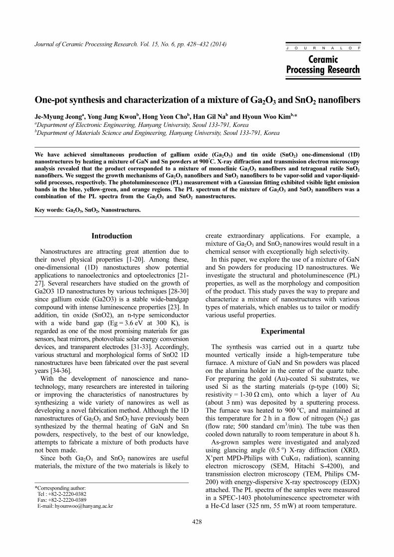
Fig. 2 is a low magnification TEM image, indicatingthat there are two types of 1D structure in the product:those without tip-nanoparticles (indicated by Arrow 1)and those with tip-nanoparticles (indicated by Arrow 2).
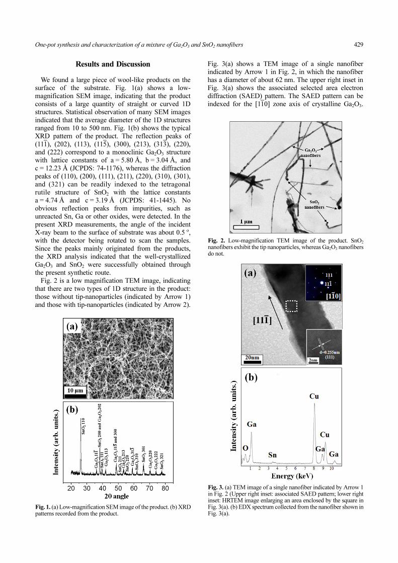
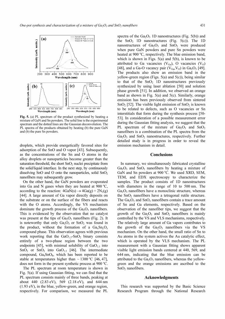
Fig. 3(a) shows a TEM image of a single nanofiberindicated by Arrow 1 in Fig. 2, in which the nanofiberhas a diameter of about 62 nm. The upper right inset inFig. 3(a) shows the associated selected area electrondiffraction (SAED) pattern. The SAED pattern can beindexed for the [110] zone axis of crystalline Ga2O3.
Fig. 1. (a) Low-magnification SEM image of the product. (b) XRDpatterns recorded from the product.
Fig. 2. Low-magnification TEM image of the product. SnO2
nanofibers exhibit the tip nanoparticles, whereas Ga2O3 nanofibersdo not.
Fig. 3. (a) TEM image of a single nanofiber indicated by Arrow 1in Fig. 2 (Upper right inset: associated SAED pattern; lower rightinset: HRTEM image enlarging an area enclosed by the square inFig. 3(a). (b) EDX spectrum collected from the nanofiber shown inFig. 3(a).

430 Je-Myung Jeong, Yong Jung Kwon, Hong Yeon Cho, Han Gil Na and Hyoun Woo Kim
The length direction of the nanofiber is along the [111]direction. The lower right inset is a high resolutionTEM (HRTEM) image enlarging an area enclosed bythe square in Fig. 3(a), revealing good crystallinity. Theinterplanar spacing is about 0.255 nm, corresponding tothe (111) plane of monoclinic Ga2O3. Fig. 3(b) showsthe typical EDX spectrum collected from the nanofibershown in Fig. 3(a). The spectrum identifies the peaksof Ga, O, Sn, and Cu. Since the Cu signals aregenerated from the TEM microgrid supporting thenanofibers, we suppose that the components of thenanofiber are Ga, O, and a trace amount of Sn. Fromthe XRD, SAED, and HRTEM observation, in whichthe nanofiber is monoclinic Ga2O3, we suggest that Snexists is an element in the Ga2O3 lattice.
Fig. 4(a) shows the TEM image of a single nanofiberindicated by Arrow 2 in Fig. 2 (average diameter~ 83 nm). The nanoparticle at the tip of the nanofiberappears dark, having high contrast compared with thenanofiber stem. The inset in Fig. 4(a) shows thecorresponding SAED pattern, which can be indexed forthe [102] zone axis of the tetragonal rutile SnO2. Fig.4(b) is the enlarged HRTEM image of the rectangularbox marked in Fig. 4(a). The interplanar spacing isapproximately 0.176 nm, corresponding to the (211)plane of the tetragonal rutile SnO2. EDX measurementsmade on the fiber tip and the fiber stem indicate thatthe tip consists of Au, Sn, O, and Ga (Fig. 4(c)), butthe stem is only composed of Sn, O, and Ga (Fig.4(d)). Accordingly, we reveal that the SnO2 nanofiberscontain a trace amount of Ga, while the nanoparticlecomprises a Au element.
In the preliminary experiments, the synthesis wascarried out under the same conditions as those in thepresent work, with the exception that only Sn powders
were used. In this case, 1D nanostructures of SnO2
without tip nanoparticles were obtained. When onlyGaN powders were used, Ga2O3 1D nanostructureswithout tip nanoparticles were obtained. In the presentwork, however, although the Ga2O3 nanofibers still donot have nanoparticles at their tips, the SnO2 nanofibersrevealed the presence of tip nanoparticles. In otherwords, it is noteworthy that the growth mechanism waschanged with the change in the source composition.SnO2 nanofibers with tip nanoparticles were notobtained when only the Sn precursors as the sourcewere used, whereas those with tip nanoparticles wereproduced by using a mixture of GaN and Sn powders.
We suppose that the mixing of the source powders willaffect the growth mechanism. In general, there are twomain growth mechanisms of 1D nanostructures: vapor-liquid-solid (VLS) and vapor-solid (VS) mechanisms. Itis expected that the growth mode is dependent on theexperimental condition. In the VLS mode, the generatedvapor combines with Au on the substrate and thesupersaturation of the liquid alloy droplet brings aboutthe precipitation of short nuclei from which thenanowires may subsequently grow [37]. On the otherhand, in the VS mode, the catalytic role of Au will bereduced, and the nanowires will tend to grow by directadsorption of the source vapors onto the solid substrate[38].
In a previous study, the growth temperature de-termines the relevant growth mode, in which lower andhigher temperature growth were dominated by theVLS and VS processes, respectively [38]. Highertemperature guarantees higher vapor pressure of thesource materials. Similarly, at the growth temperaturein the present work, sufficient amount of source vaporis provided. Furthermore, we expect that the relativeamount of Ga concentration is significantly greaterthan that of the Sn concentration in the vapor of thepresent system. Accordingly, most Ga vapors willdirectly adsorb on the substrate and nanowire surface,being operated by the VS process. On the other hand,the relatively small amount of Sn vapors at thattemperature will bring about a situation, in which theratio of the Sn-associated vapor to Au is expected to besufficiently small.
The existence of Au-related tip nanoparticles suggeststhat the growth of SnO2 nanofibers is mainly controlledby a VLS process, with Au originating from the pre-deposited Au layer. In the present synthetic process, liquidSn (Melting point = 232 oC) is oxidized, according to thereaction of 2Sn(l) + O2 (g) → 2SnO(g). We believe thatthe oxygen comes from the air leakage or the residualoxygen in the furnace, even though we did notintentionally introduced oxygen to the tube. The gen-erated metastable SnO gas spontaneously decomposesinto liquid Sn and solid SnO2 (2SnO(g) → SnO2(s)+ Sn(l)) [39-42]. The liquid Sn droplets fall on thesubstrate and subsequently form Sn-Au alloyed
Fig. 4. (a) TEM image of a single nanofiber indicated by Arrow 2in Fig. 2 (Inset: corresponding SAED pattern). (b) EnlargedHRTEM image of a rectangular box marked in Fig. 4(a). EDXspectra of (c) the fiber tip and (d) the fiber stem.
One-pot synthesis and characterization of a mixture of Ga2O3 and SnO2 nanofibers 431
droplets, which provide energetically favored sites foradsorption of the SnO and O vapor [43]. Subsequently,as the concentrations of the Sn and O atoms in thealloy droplets or nanoparticles become greater than thesaturation threshold, the short SnO2 nuclei precipitate fromthe solid/liquid interface. In the next step, by continuouslydissolving SnO and O onto the nanoparticles, solid SnO2
nanofibers may subsequently grow. On the other hand, the GaN powders are evaporated
into Ga and N gases when they are heated at 900 oC,according to the reaction: 4GaN(s) → 4Ga(g) + 2N2(g)[44]. A large amount of Ga vapor directly deposits onthe substrate or on the surface of the fibers and reactswith the O atoms. Accordingly, the VS mechanismdominate the growth process of the Ga2O3 nanofibers.This is evidenced by the observation that no catalystwas present at the tips of Ga2O3 nanofibers (Fig. 2). Itis noteworthy that only Ga2O3 or SnO2 was found inthe product, without the formation of a GaxSnyOz
compound phase. This observation agrees with previouswork reporting that the GaO1.5-SnO2 binary consistsentirely of a two-phase region between the twoendpoints [45], with minimal solubility of GaO1.5 intoSnO2 or SnO2 into GaO1.5 [46]. The intermediatecompound, Ga4SnO8, which has been reported to bestable at temperatures higher than ~ 1300 oC [46, 47],does not form in the present synthetic process at 900 oC.
The PL spectrum at room temperature is shown inFig. 5(a). If using Gaussian fitting, we can find that thePL spectrum consists mainly of three bands, peaking atabout 440 (2.83 eV), 569 (2.18 eV), and 644 nm(1.93 eV), in the blue, yellow-green, and orange region,respectively. For comparison, we measured the PL
spectra of the Ga2O3 1D nanostructures (Fig. 5(b)) andthe SnO2 1D nanostructures (Fig. 5(c)). The 1Dnanostructures of Ga2O3 and SnO2 were producedwhen pure GaN powders and pure Sn powders wereheated at 900 oC, respectively. The blue emission band,which is shown in Figs. 5(a) and 5(b), is known to beattributed to Ga vacancies (VGa), O vacancies (VO)[48], and a Ga-O vacancy pair (VGa,VO) in Ga2O3 [49].The products also show an emission band in theyellow-green region (Figs. 5(a) and 5(c)), being similarto that of the SnO2 1D nanostructures previouslysynthesized by using laser ablation [50] and solutionphase growth [51]. In addition, we observed an orangeband as shown in Fig. 5(a) and 5(c). Similarly, orangeemission has been previously observed from sinteredSnO2 [52]. The visible light emission of SnO2 is knownto be related to defects, such as O vacancies or Sninterstitials that form during the synthesis process [50-53]. In consideration of a possible measurement errorduring the Gaussian fitting analysis, we suggest that thePL spectrum of the mixture of Ga2O3 and SnO2
nanofibers is a combination of the PL spectra from theGa2O3 and SnO2 nanostructures, respectively. Furtherdetailed study is in progress in order to reveal theemission mechanism in detail.
Conclusions
In summary, we simultaneously fabricated crystallineGa2O3 and SnO2 nanofibers by heating a mixture ofGaN and Sn powders at 900 oC. We used XRD, SEM,TEM, and EDX spectroscopy to characterize thesamples. The product consists of 1D nanostructureswith diameters in the range of 10 to 500 nm. TheGa2O3 nanofibers have a monoclinic structure, whereasthe SnO2 nanofibers have a tetragonal rutile structure.The Ga2O3 and SnO2 nanofibers contain a trace amountof Sn and Ga elements, respectively. Based on theobservation of the nanofiber tips, we suggest that thegrowth of the Ga2O3 and SnO2 nanofibers is mainlycontrolled by the VS and VLS mechanisms, respectively.The relatively large amount of Ga vapors contributes tothe growth of the Ga2O3 nanofibers via the VSmechanism. On the other hand, the small ratio of Sn toAu atoms in the system actives the Au catalytic effect,which is operated by the VLS mechanism. The PLmeasurement with a Gaussian fitting shows apparentvisible light emission bands centered at 440, 569, and644 nm, indicating that the blue emission can beattributed to the Ga2O3 nanofibers, whereas the yellow-green and the orange emissions are ascribed to theSnO2 nanofibers.
Acknowledgments
This research was supported by the Basic ScienceResearch Program through the National Research
Fig. 5. (a) PL spectrum of the product synthesized by heating amixture of GaN and Sn powders. The solid line is the experimentalspectrum and the dotted lines are the Gaussian deconvolution. ThePL spectra of the products obtained by heating (b) the pure GaNand (b) the pure Sn powders.
432 Je-Myung Jeong, Yong Jung Kwon, Hong Yeon Cho, Han Gil Na and Hyoun Woo Kim
Foundation of Korea (NRF) funded by the Ministry ofEducation, Science and Technology (2011-0009946).
References
1. R. Kuar, M. C. Mishra, B. K. Sharma, V. Vyas and G.Sharma, Electron. Mater. Lett. 9 (2013) 19-23.
2. H.-W. Cui, D.-S. Li and Q. Fan, Electron. Mater. Lett. 9(2013) 1-5.
3. M. A. Majeed Khan, W. Khan, M. Ahamed, M. S. Alsalhiand T. Ahmed, Electron. Mater. Lett. 9 (2013) 53-57.
4. R. Sabbaghizadeh and M. Hashim, Electron. Mater. Lett. 9(2013) 115-118.
5. D. Soundararajan, Y. Lim, M.-P. Chen and K. H. Kim,Electron. Mater. Lett. 9 (2013) 177-182.
6. T. Prakash, S. Ramasamy and B. S. Murty, Electron. Mater.Lett. 9 (2013) 207-211.
7. A. Mondal, J. C. Dhar, P. Chinnamuthu, N. K. Singh, K. K.Chattopadhay, S. K. Das, S. Ch Das and A. Bhattachayya,Electron. Mater. Lett. 9 (2013) 213-217.
8. S. N. Heo, K. Y. Park, Y. J. Seo, F. Ahmed, M. S. Anwarand B. H. Koo, Electron. Mater. Lett. 9 (2013) 261-265.
9. S. Sharma and S. Chawla, Electron. Mater. Lett. 9 (2013)267-271.
10. K. Seo, M. Suh and S. Ju, Electron. Mater. Lett. 9 (2013)273-277.
11. C.-H. Lee, D.-J. Choi and Y.-J. Oh, Electron. Mater. Lett. 9(2013) 283-286.
12. Y. Jia, F. Yang, F. Cai, C. Cheng and Y. Zhao, Electron.Mater. Lett. 9 (2013) 287-291.
13. S. Kim, G. Nam, K. G. Yim, J. Lee, Y. Kim and J.-Y. Leem,Electron. Mater. Lett. 9 (2013) 293-298.
14. H.-W. Cui, D.-S. Li and Q. Fan, Electron. Mater. Lett. 9(2013) 299-307.
15. H. Lee, J.-H. Shin, J. Chae, J. B. Kim, T.-H. Kim and K.-B.Park, Electron. Mater. Lett. 9 (2013) 357-362.
16. S. Kumar, P. Dharma and V. Sharma, Electron. Mater. Lett.9 (2013) 371-374.
17. T. Sreesattabud, B. J. Gibbons, A. Watcharapasom and S.Jiansirisomboon, Electron. Mater. Lett. 9 (2013) 409-412.
18. N.-M. Park, J. Shin, B. Kim, K. H. Kim and W.-S. Cheong,Electron. Mater. Lett. 9 (2013) 467-469.
19. C.-G. Kuo, H. Chang, L.-R. Hwang, S. Hor, J.-S. Chen, G.-Y. Liu and S.-C. Cheng, Electron. Mater. Lett. 9 (2013)481-484.
20. J. Huang, S. Somu and A. Busnaina, Electron. Mater. Lett.9 (2013) 505-507.
21. E. W. Wong, P. E. Sheehan and C. M. Lieber, Science 277(1997) 1971-1975.
22. J. T. Hu, T. W. Odom and C. M. Lieber, Acc. Chem. Res.32 (1999) 435-445.
23. Z. W. Pan, Z. R. Dai and Z. L. Wang, Science 291 (2001)1947-1949.
24. L. F. Dong, J. Jiao, D. W. Tuggle, J. Petty, S. A. Elliff andM. Coulter, Appl. Phys. Lett. 82 (2003) 1096-1098.
25. H. W. Seo, C.-S. Han, W. S. Jang and J. Park, Curr. Appl.Phys. 6 (2006) e216-e218.
26. S. J. Jo, D. K. Lee, M.-S. Kim, Y. H. Kim and Y. S. Kang,
Curr. Appl. Phys. 6 (2006) 781-785. 27. H. Hasegawa, Curr. Appl. Phys. 7 (2007) 318-321. 28. Y. C. Choi, W. S. Kim, Y. S. Park, S. M. Lee, D. J. Bae, Y.
H. Lee, G. S. Park, W. B. Choi, N. S. Lee and J. M. Kim,Adv. Mater. 12 (2000) 746-750.
29. C. H. Liang, G. W. Meng, G. Z. Wang, Y. W. Wang, L. D.Zhang and S. Y. Zhang, Appl. Phys. Lett. 78 (2001) 3202-3204.
30. G. Gundiah, A. Govindaraj and C. N. R. Rao, Chem. Phys.Lett. 351 (2002) 189-194.
31. Z. M. Jarzebski and J. P. Maraton, J. Electrochem. Soc. 123(1976) 199-205.
32. Q V. Vasu and A. Subrahmanyam, Thin Solid Films 193/194 (1990) 973-980.
33. A. Tsunashima, J. Mater. Sci. 21 (1986) 2731-2734. 34. R.-Q. Zhang, Y. Lifshitz and S.-T. Lee, Adv. Mater. 15
(2003) 635-640.35. Z. L. Wang and Z. Pan, Adv. Mater. 14 (2002) 1029-1032. 36. Y. Liu, C. Zheng, W. Wang, C. Yin and G. Wang, Adv.
Mater. 13 (2001) 1883-1887. 37. H. W. Kim, M. A. Kebede, H. S. Kim, H. G. Na, J. C.
Yang, C. Lee, Met. Mater. Int. 16 (2010) 87-91. 38. S. S. Kim, J. Y. Park, H. S. Kim, H. G. Na, J. C. Yang, S.
H. Shim, C. Lee, D. Park, D. Nam, H. Cheong, H. W. Kim,J. Phys. D: Appl. Phys. 44 (2011) b025502.
39. J. Q. Hu, X. L. Ma, N. G. Shang, Z. Y. Xie, N. B. Wong, C.S. Lee and S. T. Lee, J. Phys. Chem. B 106 (2002) 3823-3826.
40. D.-W. Yuan, R.-F. Yan and G. Simkovich, J. Mater. Sci. 34(1999) 2911-2920.
41. J. C. Nover and F. D. Richardson, Trans. Inst. Min. Metall.81 (1972) 63.
42. Z. R. Dai, Z. W. Pan and Z. L. Wang, Adv. Funct. Mater.13 (2003) 9-24.
43. J. X. Wang, D. F. Liu, X. Q. Yan, H. J. Yuan, L. J. Ci, Z. P.Zhou, Y. Gao, L. Song, L. F. Liu, W. Y. Zhou, G. Wang andS. S. Xie, Solid State Commun. 130 (2004) 89-94.
44. J.-S. Lee, K. Park, S. Nahm, S.-W. Kim and S. Kim, J.Cryst. Growth 244 (2002) 287-295.
45. G. B. Palmer and K. R. Poeppelmeier, Solid State Sci. 4(2002) 317-322.
46. D. D. Edwards and T. O. Mason, J. Am. Ceram. Soc. 81(1998) 3285-3292.
47. M. B. Varfolomeev, A. S. Miranova, T. I. Dudina andKoldashov, Russ. J. Inorg. Chem. 20 (1975) 1738.
48. L. F. Dong, J. Jiao, M. Coulter and L. Love, Chem. Phys.Lett. 376 (2003) 653-658.
49. N. Sakulchaicharoen and D. E. Resasco, Chem. Phys. Lett.377 (2003) 377-383.
50. J. Hu, Y. Bando, Q. Liu and D. Goldberg, Adv. Funct.Mater. 13, (2003) 493-496.
51. B. Cheng, J. M. Russell, W. Shi, L. Zhang and E. T.Samulski, J. Am. Chem. Soc. 126 (2004) 5972-5973.
52. D. Maestre, A. Cremades and J. Piqueras, J. Appl. Phys. 95(2004) 3027-3030.
53. S.-S. Chang and D. K. Park, Mater. Sci. Eng. B 95 (2002)55-60.


![[ APPLICATION ] - Apr. 17, 2020 ACURA - Yellow Speed · 2020-05-19 · 286mm x 24mm disc 330mm x 28mm disc 6 POT (YSCPF6d) 4 POT (YSCPF4a) 6 POT (YSCPF6a) 4 POT (YSCPF4a) 6 POT (YSCPF6a)](https://img.pdfslide.us/doc/110x75/5f27b6269f054979e351952e/-application-apr-17-2020-acura-yellow-2020-05-19-286mm-x-24mm-disc-330mm.jpg)