Embed Size (px)
Citation preview

One-Dimensional Electron Systems at Surfaces
Physics in one dimension :
• Elegant and simple
• Lowest dimension with translational motion
• Electrons cannot avoid each other

1D : • Collective excitations• Spin-charge separation
Giamarchi, Quantum physics in one dimension
2D,3D :• Electrons avoid each other

Localized e- (real space)Hubbard, t-J Models
• Different velocities for spin and charge
• Holon and spinon bands intersect at EF
Two Views of Spin Charge Separation
Holon
Hole
Spinon
EF
k
E
Spinon
Holon
Delocalized e- (k-space)Tomonaga-Luttinger Model

Atomic Chains as the Ultimate Nanowires
• Straight steps at vicinal Si(111)7x7( 1 kink in 20 000 edge atoms )
• Metallic surface states in the gap of silicon (truly 2D)

Clean
"Decoration" of Steps⇒ 1D Atomic Chains
With Gold1/5 monolayer
Si chain
Si dopant
x-Derivative of the Topography, “ Illumination from the Left ”

Many metals create chains
Li, Na,…Ca,Ba,…In Ag, AuPt Gd,Ho,Dy,Ce
Also on Si(100), GaAs(110)

Au
Graphitichoneycomb chain
drives the surface one-dimensional
Variable chain
spacing, coupling

2D
Fermi Surfaces from 2D to 1D
2D + super-lattice
1D

t1/t2 ≈ 40 10
kx
1D/2D Coupling Ratio
Tight Binding Model
Fermi Surface Data
t1/t2 is variable from 10:1 to > 70:1 via the step spacing
t2
t1

8/3 e- per chain atom (spins paired)5/3 e- per chain atom (spin split)
Crain et al., PRL 90, 176805 (2003)
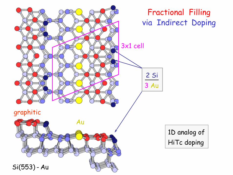
Fractional Filling
Augraphitic
Fractional Fillingvia Indirect Doping
1D analog of HiTc doping
Si(553) - Au
3x1 cell
2 Si3 Au

Fractional Chargeat the End of a CDW / Chain Segment
Seen for 2x1 (polyacetylene) : Su, Schrieffer, HeegerPR B 22, 2099 (1980)
Predicted for 3x1 : Su, SchriefferPRL 46, 738 (1981)
Suggested for Si(553)3x1-Au : Snijders et al.PRL 96, 076801 (2006)

Is there Spin-Charge Separation ?
Bands remain split at EF
⇒ Not Spinon + Holon
Losio et al., PRL 86, 4632 (2001)
Why two half-filled bands ?~ two half-filled orbitals
~ two broken bonds
EF
Proposed by
Segovia et al., Nature 402, 504 (1999)
Si(557) - Au
hν= 34 eV
E [eV]

Sanchez-Portal et al. PRL 93, 146803 (2004)
LDA Calculation Predicts Spin Splitting
Non-magnetic constituents !
Adatoms
Step Edge
Si-Au Antibonding
Si-Au Bonding
E (eV)
0 ZB1x1
Adatoms
ZB2x1
kx
EFSpin-split band, similar to that in photoemission
Si(557) - Au

Si AdatomsAu
GraphiticHoneycomb
Chain
First Principles Calculations:Crain, Erwin, et al.,PRB 69, 125401 (2004) Sanchez-Portal et al.,PRB 65, 081401 (2002)
X-Ray Diffraction:Robinson et al., PRL 88, 096104 (2002)
Spin-Split Band
Si(557) - Au

Evidence for Spin–Splitting
E [eV]
kx [Å−1]
• Avoided crossings located left / right for spin-orbit (Rashba) splitting.
• Would be top / bottom for non-magnetic, (anti-)ferromagnetic splittings.
Barke et al., PRL 97, 226405 (2006)
Si(553) - Au

Nanoscale Phase Separation in 1D
1 Erwin, PRL 91, 206101 (2003) 2 McChesney et al., Phys. Rev. B 70, 195430 (2004)
Si(111)5x2 - Au
• Doped and undoped segments ( 1D version of “stripes” )gap ! metallic
• Competition between optimum doping1 (5x8)and Fermi surface nesting2 (5x4)
• Compromise: 50/50 filled/empty (5x4) sections

What Determines theLength of the Segments ?
Barke et al., unpublished
Spectroscopy +0.8V
-1.2V Topography +0.8V

Use semiconductor substrates
• Metal atoms locked to the substrate
• Electrons at EF decouple (in the gap)
• Tunable band filling, fractional 5/3
• Tunable chain coupling, 10:1 to >70:1
• Tunable magnetic moment (rare earths)
⇒ New playground for low-dimensional physics
Overview: Crain and Himpsel, Appl. Phys. A 82, 431 (2006)