Embed Size (px)
Citation preview

DesignCon 2010
On-Chip Power Supply Noise and
Reliability Analysis for Multi-Gigabit
I/O Interfaces
Ralf Schmitt, Rambus Inc. [Email: [email protected]]
Hai Lan, Rambus Inc.
Ling Yang, Rambus Inc.

Abstract
Verifying the power supply quality of the interface PHY is crucial to achieve multi-
Gigabit data rates. The nature of high-speed interfaces, which are large mixed-signal full-
custom designs, are challenging for commercial EDA tools. We are presenting an on-chip
supply analysis flow that allows us to analyze supply noise analysis even for large
interface designs with high accuracy. This analysis flow provides information for static
IR drop and transient AC noise waveforms and accurate predicts supply noise for every
device location. The results are further used to predict the impact of supply noise on the
system margin of the interface.
Authors Biography
Ralf Schmitt is Senior Engineering Manager at Rambus Inc. He received his Ph.D. in
Electrical Engineering from the Technical University of Berlin, Germany. Since 2002, he
is with Rambus Inc, Los Altos, California, where he is a senior engineering manager
responsible for signal and power integrity on chip, package, and system level. His
professional interests include signal and power integrity, timing analysis, clock
distribution, and high-speed interface design.
Hai Lan is a Senior Member of Technical Staff at Rambus Inc., where he has been
working on on-chip power integrity and jitter analysis for multi-gigabit interfaces. He
received his Ph.D. in Electrical Engineering from Stanford University, M.S. in Electrical
and Computer Engineering from Oregon State University, and B.S. in Electronic
Engineering from Tsinghua University in 2006, 2001, and 1999, respectively. His
professional interests include design, modeling, and simulation for mixed-signal
integrated circuits, substrate noise coupling, power and signal integrity, and high-speed
interconnects.
Ling Yang is Senior Staff Engineer at Rambus Inc. She received her MSEE from the
University of Illinois Urbana-Champaign. Since 2000, she is with Rambus Inc, Los Altos,
California, where she is responsible for power integrity for on chip, system
measurements, and signal integrity at package and system level. Her professional
interests include on-chip signal integrity, power integrity, clock distribution, board and
package level signal integrity and high-speed system measurements.

I. Introduction
Power integrity is a critical design parameter for modern high-speed I/O interface
systems. Operating at data rates in the Gigabit range requires high-quality supply
voltages, achieved by careful optimization of the power supply system on silicon,
package, and PCB. In the on-chip power delivery network, supply noise is primarily
generated through two effects: The first contribution of on-chip supply noise is caused
the resistance of the on-chip power supply grid, which is in general much higher than the
supply resistance in the package or the PCB. Drawing circuit currents through the
resistive power grid causes IR drops, reduce the voltage available at the circuit. The
second contribution of on-chip supply noise is due to the is the non-zero Power Supply
Impedance ZPDN(f), dominated by the interaction between inductance package inductance
and on-chip decoupling capacitors, which generates supply fluctuations as a response to
current changes in the system. Both supply noise contributions have to be analyzed to
assure that the system meets the Power Integrity requirements necessary to achieve the
target performance.
On-chip power integrity is a challenge for all silicon designs, not only for high-speed
I/O interfaces. As a result, the EDA industry has developed tools to support the analysis
of on-chip supply noise. The primary target of these tools is usually large SoC (System
on Chip) designs that are dominated by digital circuit blocks. High-speed I/O Interface
systems, however, have characteristics that are quite different from usual SoC designs
and which make the on-chip power supply analysis more challenging. High-speed
interface systems are mixed-signal by nature, containing many analog circuit blocks
generated in a full-custom design methodology. Estimating the device currents in such a
design requires analog or mixed-signal simulations, quite different from the cell current
estimation of digital gates used in most EDA tools. Additionally, I/O interface systems
are often very large, covering a substantial portion of the total chip area, making a
simulation of the circuits, using analog or mixed-signal simulators, even more
challenging. Finally, the accuracy requirement for the supply noise analysis are very
high, usually much higher than for digital circuits, due to the high sensitivity of high-
speed I/Os to supply noise.
We are presenting a Power Integrity analysis strategy that allows us to analyze supply
quality for large mixed-signal interface systems with an accuracy required for high-speed
I/O data rates. In this analysis flow, we are combining the current results from external
simulations, used for the verification of individual circuit blocks, with the power grid
analysis capability of a commercial EDA tool. Special attention is paid to the current
distribution inside individual circuit blocks. We will show how a strategy that uses a
gradual improvement of current assignment resolution is used to provide supply noise
results of increasing accuracy during the maturity of the design. We will also show how
the current assignment refinement process can be used to resolve false violations of IR
drop hot spots and electro-migration violations.
Using the presented current assignment strategy we can achieve supply noise
prediction, both for IR drop as well as for AC noise, with a resolution down to every

single device in the design. Using these local supply noise waveforms, we are able to
predict the Power Supply Induced Jitter in the I/O interface.
II. On-chip PI Analysis Challenges
II.1. PI Analysis Requirements
Power supply noise has significant impact on the performance of electronic systems in
general and of interface systems in particular. Supply noise generates timing variations
inside the interface link that cause jitter and reduce the timing margin of the interface
system. If supply noise gets larger, it can also generate signal distortions, reducing the
voltage margin of the interface system, and eventually cause functional failures in the
system. The Power Distribution Network (PDN) has to provide power supplies of
sufficient quality to meet the functionality and performance targets of the electronic
system [1], [2].
Figure 1 shows the range of possible supply voltages at a system component and an
example waveform. The supply voltage varies over time around an average voltage
which can be different from the nominal supply voltage, e.g. due to component tolerances
in the Voltage Regulator Module or voltage drops due to resistance in the supply path.
Figure 1: Supply Voltage over Time at Silicon Device (Example)
Silicon devices are designed to operate over a range of parameter variations for
Process, Supply Voltage, and Temperature (PVT variations). Extensive simulations are
used to verify that the device will function for any combination of PVT parameters the
device might encounter during operation. The voltage range for these simulations covers
the entire range of possible supply voltage values at the device generated by DC offset as
well as AC noise. Power Integrity analysis has to verify that the supply voltage stays in
this pre-defined supply voltage range for all operating conditions to assure the
functionality of the system over the PVT variation range.

Meeting the „voltage range‟ requirement, however, does not necessarily guarantee
system performance, especially not for high-speed I/O systems. Simulations over the
PVT variation range verify that the circuit will function correctly for any voltage in the
specified range, but these simulations assume a constant supply voltage over time.
Changes of the supply voltage over time, shown as AC supply noise in Figure 1, can
cause delay variations in circuit components and signal waveform distortions that are not
covered by PVT corner simulations. For example, Power Supply Induced Jitter (PSIJ)
caused by AC supply noise is a major source of jitter in electronic systems and can limit
the achievable clock frequency of devices as well as the data rate of I/O interface
systems. The sensitivity of system performance to AC supply noise is often a strong
function of the noise frequency itself. Supply noise of equal amplitude can have very
different impact on the system performance, depending on the frequency of the noise.
Power Integrity analysis, therefore, also has to analyze the spectrum of supply noise, to
verify that the noise impact on system margin is well inside the pre-defined budget for
this component in this system.
II.2. On-Chip Power Supply Noise Contributions
The on-chip power distribution contributes to supply noise primarily in two separate
frequency ranges: at DC and at medium to high frequencies (>100 MHz) [2].
On-chip wires are highly resistive, due to the very thin on-chip metal layers, causing
resistive voltage loss (IR drop) on the on-chip power grid. In contrast to IR drop in PCB
and package, on-chip IR drop is location dependent, i.e. some circuits, close to supply
pads, might see no IR drop at all while other circuits, far away from supply pads,
experience the maximum possible IR drop. It is therefore not possible to compensate on-
chip IR drop by raising the nominal voltage.
Additionally, switching activity of on-chip circuits generates high-frequency supply
noise, which is controlled using on-chip capacitors. The capacitance of the on-chip
supply system also affects supply noise during package/chip resonance at medium
frequencies. During package/chip resonance, the inductance of the package supply,
together with inductance contributions from the PCB environment, creates an LC
resonance with the capacitance of the on-chip power distribution system. This resonance
can generate excessive supply nose when excited by the system. The frequency and
amplitude of noise during package/chip resonance is dependent on the supply design at
the PCB, the package, and the on-chip supply network as well as the circuit activity
exciting this resonance in the system.
II.3. On-Chip PI Analysis Steps
The following PI analysis steps are required to analyze the on-chip supply system for
high-speed I/O interfaces:
Static IR drop analysis:
In this analysis, the power supply network is extracted as a resistive network. Ideal
voltage sources are attached to the supply pads, and static (average) currents are
assigned to all circuits. The resulting map of IR drops in the on-chip power supply

networks reveals weaknesses in the design of the power supply grid. It is usually the
first test of the on-chip power supply design.
Dynamic IR drop analysis
In the dynamic analysis, the on-chip power supply network is extracted together with
decoupling capacitances in the power grid itself as well as in the circuits attached to
the grid. The supply pads are connected to an ideal voltage source through an
equivalent model of the package and PCB decoupling network, and transient currents
are assigned to the circuits on the chip. The results of this analysis are transient supply
noise waveforms for the circuit activity used in this analysis.
Dynamic IR drop analysis provided feedback about the amount and correct placement
of on-chip decoupling capacitors that cannot be obtained by the static IR drop
analysis. It also provides insight into the noise spectrum, which is an important input
for the estimation of PSIJ discussed later. It requires, however, significantly more
analysis time as a static IR drop run and more design insight to provide the required
dynamic current waveforms for all circuits. For the design of high-speed I/O
interfaces, however, the results of this analysis are essential for the optimization of the
supply system.
Electromigration analysis in the supply grid (PowerEM)
Additional to static and dynamic IR drop analysis, designs usually require an analysis
of electromigration risk in the design. Electromigration describes the effect of
electrons colliding with particles in the conducting metal structure, moving some of
these particles along the direction of current flow. Over time, this material transport
can cause gaps in the on-chip wires and vias, interrupting the connection and causing a
permanent failure on this chip. For a given temperature the rate of material transport is
dependent on the current density. Therefore limits are defined to the current density in
every metal and via segment of the power supply grid to ensure that the chip will be
functional for a pre-defined operation time at worst-case temperature.
Since IR drop analysis provides the amount of current in every segment of the supply
grid, PowerEM analysis can be implemented as a post-processing step of the IR drop
analysis, dividing the current in every segment by the segment width to calculate the
current density and comparing this density with the PowerEM limit.
II.4. On-Chip PI Simulation Strategy
Simulating a large circuit in its power supply environment is in most cases
prohibitively expensive and only feasible for small circuit designs. A better concept,
adopted by virtually all available EDA tools for PI analysis, is separating the circuit
simulations necessary for current extractions from the analysis of the power supply grid.
Figure 2 shows the principle simulation concept for a static IR drop analysis. In a first
step, all device or cell currents are analyzed using non-linear circuit simulations or
heuristic methods. In the case of static IR drop analysis only the average current has to be
estimated. Since the average current of a cell or device is dependent on the actual supply
voltage seen by this cell/device, the cell/device currents are estimated as a function of
supply voltage.

Figure 2: Typical Static IR Drop Analysis Strategy
In the next step, the resistance network of the power supply grid is extracted. The
cells/devices are replaced by current sources, reflecting the cell/device currents
previously extracted for the local voltage in the power grid at the cell/device position.
Ideal voltage sources are connected at the positions of supply pads. The resulting netlist
can be solved, calculating the voltage at every power grid node, using a fast and
computational efficient linear solver.
Figure 3 shows the principle simulation concept for dynamic IR drop analysis.
Figure 3: Typical Dynamic IR Drop Analysis Strategy
In contrast to static IR drop, which only requires average currents for each cell/device
at a given voltage, dynamic IR drop analysis requires current waveforms over a switching
or timing cycle. It also requires a more complicated power grid model, including
capacitances and (optional) inductances, and it requires an equivalent model of the

package and system level supply network. But although dynamic IR analysis uses a much
more complicated simulation model than static IR drop analysis, it still follows the same
basic strategy of separating cell/device current extraction and power grid simulation.
II.5. PI Analysis Challenges of High-Speed I/O Interfaces
There are commercial design tools available from several EDA companies that address
the Power Integrity analysis steeps described above. Virtually all of these tools, in
particular all tools that are targeting large designs, are using the analysis strategy
described in Figure 2 and 3, separating the cell/device current extraction from the power
grid simulation. Many of these tools are primarily targeting digital SoC designs. The
current waveforms of individual digital gates can be easily characterized for different
switching conditions, and different algorithms and heuristics are available to estimate the
switching distribution even in large designs.
High-speed I/O interfaces are quite different from digital SoC designs. Figure 4 shows
the design hierarchy of a typical high-speed parallel interface design. High-speed I/O
interfaces, especially wide parallel interfaces, are large mixed-signal designs, following a
hierarchical full-custom design style. It consists of a mix of digital, analog, and mixed-
signal circuit blocks with many hierarchy levels. The size of these interface designs can
be substantial, exceeding more than 10% of the entire chip area, and make it prohibitive
to simulate the entire interface with a general-purpose simulation tool like Spice.
Figure 4: Design Hierarchy of High-Speed I/O Interface Design
The design style of these interface systems pose new challenges to some of the model
extraction steps of the PI analysis:
Supply Grid Extraction:
There are only minor differences in this step between SoC designs and high-speed
I/Os. SoC designs often extract the power grid only down to the power pins of (digital)
cells, while in high-speed I/O designs the power grid has to be extracted down to the
individual contacts of devices. Both extraction requirements are usually supported by
commercial PI tools.

Device Capacitance Extraction:
Extracting intentional decoupling cells is the same for SoC and for I/O designs. The
extraction of intrinsic capacitance, however, is very different for digital and analog
circuits. Intrinsic capacitance is the capacitance of circuits that are currently not active.
The extraction algorithm in PI tools is usually targeting digital gate designs and is not
easily applicable for mixed-signal designs of I/O systems.
Cell/Device Current Extraction:
Extracting cell/device currents is the largest challenge for on-chip PI analysis of I/O
designs. The currents of digital gates, which are used in SoC designs, are easy to
extract gate by gate using a simple circuit simulation or an easy heuristic estimation.
For mixed-signal circuits, however, an analog simulation of an entire circuit block is
necessary to extract device currents. This requires an understanding of the design that
is not available for an automated tool.
Extracting accurate device currents and importing these currents into the PI analysis is
the biggest challenge for the PI analysis of I/O designs. In the next section we will
discuss in detail how this problem can be addressed to achieve hogh-quality analysis
results in a high-speed I/O design.
III. Power Integrity Analysis Flow for I/O Design
As discusses earlier, the on-chip Power Integrity analysis of high-speed I/O designs
has to meet the following requirements:
Verify that the design meets the Power Supply Budget
For on-chip PI analysis this means verifying that static IR drop and on-chip AC noise
are meeting the budget allocated for these components.
Meet the reliability target of the chip design
In order to meet the target reliability over the projected lifetime of the system, all
metal connection in the chip design have to meet the EM limits for this lifetime target
(“Power On Hours”, POH). The analysis of EM risks in supply lines, PowerEM
analysis, is a post-processing step of the (static and dynamic) IR drop analysis.
However, as will be discussed later in this section, it requires a very accurate current
assignment in the design to avoid false violations, and therefore has an impact on the
current assignment strategy for high-speed I/O designs.
Meet the link jitter requirements of the interface design
One important source of link jitter is supply noise, causing “Power Supply Induced
Jitter” (PSIJ). Since PSIJ is a strong function of the noise spectrum, on-chip PI
analysis of high-speed I/O designs has to estimate not only the AC noise amplitude,
but also the spectrum of this noise.
Commercial on-chip PI tools provide functionality for each of these requirements.
However, the Pi analysis of high-speed I/O design requires from these tools a
combination of large capacity and high accuracy that is difficult to match for the
hierarchical full-custom designs style of high-speed I/O interfaces. Tools that separate the
cell/device current extraction from the simulation step, described in Figures 2 and 3, have
enough capacity to analyze large I/O designs, but current extraction is a severe challenge.
In contrast, tools derived from fast circuit simulators that simulate the entire design in its
supply environment can predict accurate currents even in full-custom mixed-signal
designs, but they are limited to designs much smaller than many I/O interfaces.
For the accurate analysis of high-speed I/O interfaces we need a combination of both
concepts that combines the current estimation of circuit-level simulations with the
capacity of a fast power grid analysis with pre-defined current profiles. In the following
sections we will present PI analysis flows addressing these challenges.
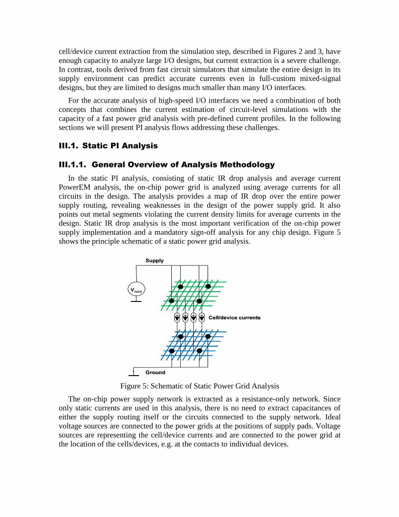
III.1. Static PI Analysis
III.1.1. General Overview of Analysis Methodology
In the static PI analysis, consisting of static IR drop analysis and average current
PowerEM analysis, the on-chip power grid is analyzed using average currents for all
circuits in the design. The analysis provides a map of IR drop over the entire power
supply routing, revealing weaknesses in the design of the power supply grid. It also
points out metal segments violating the current density limits for average currents in the
design. Static IR drop analysis is the most important verification of the on-chip power
supply implementation and a mandatory sign-off analysis for any chip design. Figure 5
shows the principle schematic of a static power grid analysis.
Figure 5: Schematic of Static Power Grid Analysis
The on-chip power supply network is extracted as a resistance-only network. Since
only static currents are used in this analysis, there is no need to extract capacitances of
either the supply routing itself or the circuits connected to the supply network. Ideal
voltage sources are connected to the power grids at the positions of supply pads. Voltage
sources are representing the cell/device currents and are connected to the power grid at
the location of the cells/devices, e.g. at the contacts to individual devices.
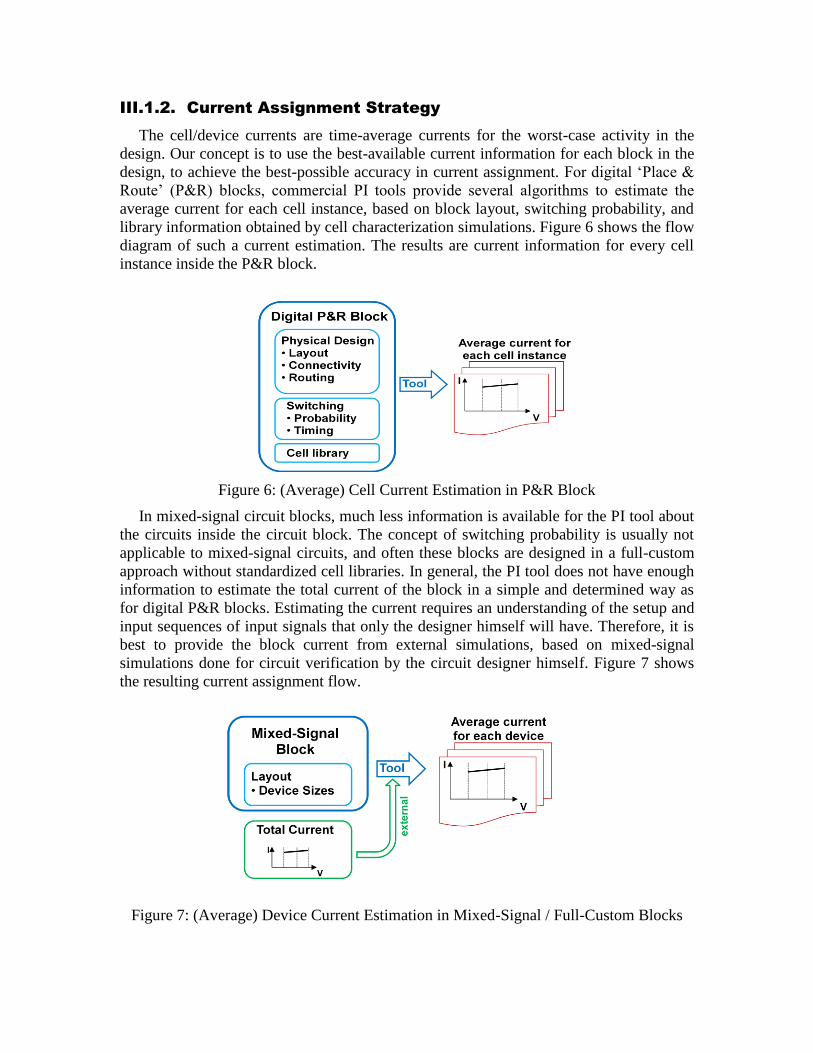
III.1.2. Current Assignment Strategy
The cell/device currents are time-average currents for the worst-case activity in the
design. Our concept is to use the best-available current information for each block in the
design, to achieve the best-possible accuracy in current assignment. For digital „Place &
Route‟ (P&R) blocks, commercial PI tools provide several algorithms to estimate the
average current for each cell instance, based on block layout, switching probability, and
library information obtained by cell characterization simulations. Figure 6 shows the flow
diagram of such a current estimation. The results are current information for every cell
instance inside the P&R block.
Figure 6: (Average) Cell Current Estimation in P&R Block
In mixed-signal circuit blocks, much less information is available for the PI tool about
the circuits inside the circuit block. The concept of switching probability is usually not
applicable to mixed-signal circuits, and often these blocks are designed in a full-custom
approach without standardized cell libraries. In general, the PI tool does not have enough
information to estimate the total current of the block in a simple and determined way as
for digital P&R blocks. Estimating the current requires an understanding of the setup and
input sequences of input signals that only the designer himself will have. Therefore, it is
best to provide the block current from external simulations, based on mixed-signal
simulations done for circuit verification by the circuit designer himself. Figure 7 shows
the resulting current assignment flow.
Figure 7: (Average) Device Current Estimation in Mixed-Signal / Full-Custom Blocks

The PI tool is used to distribute the total block current to the devices inside the circuit
block. This allows a device-level current assignment, necessary for a complete IR drop
and PowerEM analysis of the entire supply network, based on block-level current
assignments. Depending on the used PI tool different strategies are available for this
current distribution.
All of these strategies are using the device sizes in the design to identify how the total
current will likely distribute between different devices. They do not distinguish between
different circuit topologies like digital gates and analog circuits, although in reality the
current for a given device size can be vary substantially dependent on the circuit this
device is used in.
In order to analyze the accuracy of current assignment inside a large circuit block
using a PI tool algorithm, we assigned current to the toplevel block of a large design and
used the PI tool to distribute the current inside the entire design. We then compared the
currents assigned to sub-blocks with circuit simulations results that were used predict the
total toplevel block current. Figure 8 shows the result of this comparison.
Figure 8: Comparison of sub-block currents using PI tool vs. circuit simulations
Figure 8 shows that there are large differences between the sub-block currents
distributed by the PI tool and simulated using circuit simulations. A detailed analysis
showed that most of these differences were caused by two issues:
Large devices (e.g. power clamps) with little current during normal operation
Too much current assigned to digital circuits, too little current assigned to analog
circuits, in mixed-signal blocks.
This experiment shows that a block-level current assignment as used in our flow needs
a way to refine the distributions of currents to sub-blocks. In particular, it is necessary to
assign small currents to sub-blocks or devices with known little current dissipation, and it
is also necessary to assign currents explicitly to separate analog or digital sub-blocks
inside a larger mixed-signal block.
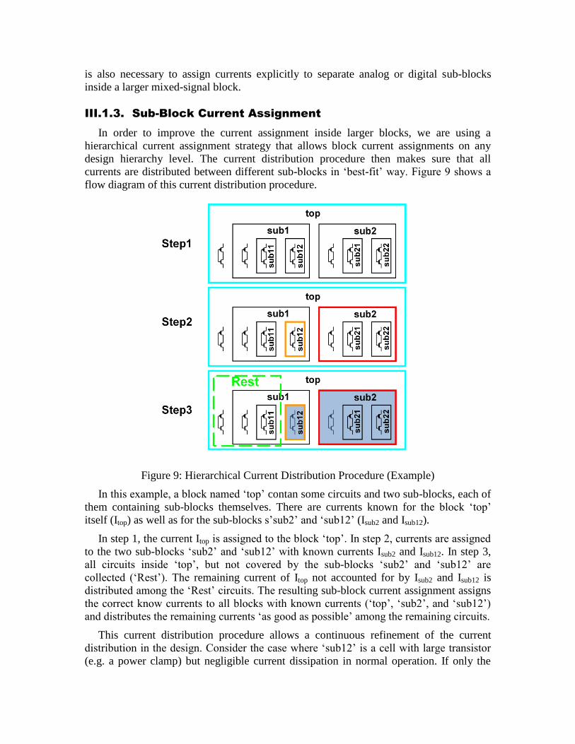
III.1.3. Sub-Block Current Assignment
In order to improve the current assignment inside larger blocks, we are using a
hierarchical current assignment strategy that allows block current assignments on any
design hierarchy level. The current distribution procedure then makes sure that all
currents are distributed between different sub-blocks in „best-fit‟ way. Figure 9 shows a
flow diagram of this current distribution procedure.
Figure 9: Hierarchical Current Distribution Procedure (Example)
In this example, a block named „top‟ contan some circuits and two sub-blocks, each of
them containing sub-blocks themselves. There are currents known for the block „top‟
itself (Itop) as well as for the sub-blocks s‟sub2‟ and „sub12‟ (Isub2 and Isub12).
In step 1, the current Itop is assigned to the block „top‟. In step 2, currents are assigned
to the two sub-blocks „sub2‟ and „sub12‟ with known currents Isub2 and Isub12. In step 3,
all circuits inside „top‟, but not covered by the sub-blocks „sub2‟ and „sub12‟ are
collected („Rest‟). The remaining current of Itop not accounted for by Isub2 and Isub12 is
distributed among the „Rest‟ circuits. The resulting sub-block current assignment assigns
the correct know currents to all blocks with known currents („top‟, „sub2‟, and „sub12‟)
and distributes the remaining currents „as good as possible‟ among the remaining circuits.
This current distribution procedure allows a continuous refinement of the current
distribution in the design. Consider the case where „sub12‟ is a cell with large transistor
(e.g. a power clamp) but negligible current dissipation in normal operation. If only the
block current Itop is known, a large amount of Itop would be assigned to „sub12‟ by the PI
tool due to the large transistor inside „sub12‟, leaving little current for the remaining
circuits inside „top‟. Assigning the correct small current Isub12 to the block „sub12‟
corrects this issue. Now almost the entire current Itop is available for the remaining
circuits outside „sub12‟.
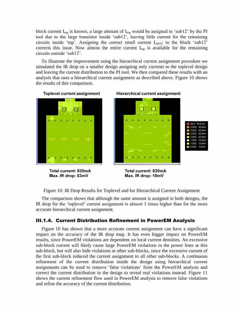
To illustrate the improvement using the hierarchical current assignment procedure we
simulated the IR drop on a smaller design assigning only currents to the toplevel design
and leaving the current distribution to the PI tool. We then compared these results with an
analysis that uses a hierarchical current assignment as described above. Figure 10 shows
the results of this comparison.
Figure 10: IR Drop Results for Toplevel and for Hierarchical Current Assignment
The comparison shows that although the same amount is assigned in both designs, the
IR drop for the „toplevel‟ current assignment is almost 3 times higher than for the more
accurate hierarchical current assignment.
III.1.4. Current Distribution Refinement in PowerEM Analysis
Figure 10 has shown that a more accurate current assignment can have a significant
impact on the accuracy of the IR drop map. It has even bigger impact on PowerEM
results, since PowerEM violations are dependent on local current densities. An excessive
sub-block current will likely cause large PowerEM violations in the power lines at this
sub-block, but will also hide violations at other sub-blocks, since the excessive current of
the first sub-block reduced the current assignment to all other sub-blocks. A continuous
refinement of the current distribution inside the design using hierarchical current
assignments can be used to remove „false violations‟ from the PowerEM analysis and
correct the current distribution in the design to reveal real violations instead. Figure 11
shows the current refinement flow used in PowerEM analysis to remove false violations
and refine the accuracy of the current distribution.

Figure 11: Current Refinement Flow for PowerEM Analysis Improvement
When a violation is reported in the PowerEM analysis, the cell that causes this
violation is identified in the layout of the design. If this cell is among the blocks with
explicit current assignment, then the cell current is correct (by construction) and the
violation has to be fixed. If, however, the cell is not among the blocks with explicit
current assignment, the expected cell current is verified using circuit simulation results. If
the assigned current was correct, the violation is real and has to be fixed. If the current
assigned to the cell was incorrect, an explicit current will be assigned to this cell in the
next analysis iteration. If the explicit current assignment does not fix this violation, it will
be re-visited after the next analysis iteration.
Using this refinement methodology, the accuracy of the analysis continually improves,
leading to more accurate IR drop and PowerEM results. This procedure is far superior to
a simple „waiver‟ process where false violations are simply ignored. In a „waiver‟
process, the same false violations are reported again in every analysis iteration, and the
inaccurate current distribution that lead to the false violations in the first place is never
corrected, leaving other „real‟ violations undetected.
III.2. Dynamic IR Drop Analysis
III.2.1. Motivation
Dynamic IR drop analysis is necessary for high-speed I/O interfaces to verify that the
design meets the AC supply noise budget. It verifies that a sufficient amount of on-chip
capacitors are available in the design to stabilize the voltage during switching activities,
and also that these capacitors are placed at the correct locations where they can
effectively suppress supply noise.

Additionally to this obvious verification purpose, which applies to any design,
dynamic IR drop analysis is especially important for high-speed I/O systems since it
allows a prediction of Power Supply Induced Jitter (PSIJ) [3].
Supply noise is an important source of link jitter in high-speed interfaces. The
magnitude and spectrum of this jitter has an impact on decisions regarding clocking
architecture and timing circuit design. A major goal of the power supply design in these
interfaces is not to minimize supply noise itself, but to minimize the impact of supply
noise on the interface performance. Understanding the AC supply noise generated in the
design and its distribution over the circuit area is an important step towards this goal.
PSIJ is largely controlled by two parameters: the power supply spectrum and the
sensitivity of the interface circuits to noise at different frequencies. Characterizing these
two parameters allows the prediction of PSIJ spectrum and total supply induced jitter in
the interface. Figure 12 shows a schematic of the prediction flow we are using for PSIJ
prediction. Details to this methodology can be found in [4].
Figure 12: PSIJ Prediction Flow
Dynamic IR drop analysis allows the prediction of the power supply spectrum seen by
the circuits that are sensitive to supply noise. It is therefore an important step in the PSIJ
prediction.
III.2.2. Flow Setup
Compared to static IR drop, there are three major differences in the analysis flow for
dynamic analysis:
The device currents are transient waveforms over time
The extraction of the on-chip power supply system has to cover R as well as C
A system-level PDN model is necessary to account for package and system inductance
in the supply path
Figure 13 shows the schematic of the dynamic IR drop analysis.

Figure 13: Schematic of Dynamic IR Drop Analysis Flow
The extraction of on-chip capacitances covers both intentional decoupling cells,
capacitor cells explicitly placed into the design, as well as intrinsic capacitance, parasitic
capacitance provided by the power routing and circuits. Intrinsic capacitance is usually
dominated by the capacitance of circuit blocks that are not active at a given time. For
digital gates, commercial tools provide algorithms to extract the average capacitance in a
larger circuit block based on the switching probability in the block. For analog and
mixed-signal circuits the intrinsic capacitance due to inactive circuits is much smaller and
much more difficult to estimate. Therefore, intrinsic capacitance is ignored in our flow
for analog and mixed-signal blocks, and the power supply design relies on explicit
decoupling capacitors for these blocks instead. This makes the analysis slightly
pessimistic, but good correlation with noise measurement results confirms that this error
is usually very small.
For dynamic IR drop analysis it is essential to include a model of the system-level
PDN system, in particular a model of the inductance introduced in the supply path by the
package inductance and the inductance of PCB capacitors close to the package. Without
this supply model, ideal voltage sources would be connected to all on-chip supply pads,
which would dramatically under-predict AC supply noise in the chip especially at high
frequencies. Using ideal voltage sources at the supply pads, unlimited current can be
provided by these sources with infinite edge rate, quickly reacting to any current spike in
the design. In reality, however, the inductance of the package and PCB supply system
limits the change of the current supply through the package. Especial for high-frequency
current changes like switching spikes the necessary charge initially has to be provided
largely by the on-chip decoupling capacitors, and the package current will only react to
current changes in the lower MHz range and below.
III.2.3. Current Extraction and Assignment Strategy
Extracting transient current waveform necessary for dynamic IR drop analysis has the
same challenges as the extraction of average currents used in static IR drop analysis. For
digital gate circuits, commercial PI tools provide different algorithms to estimate
transient current waveforms for every instance of the design. For analog or mixed-signal

circuit blocks, however, transient current waveforms have to be extracted using external
simulations to achieve a reasonable accuracy of the dynamic IR drop analysis. Figure 14
shows the flow diagram of this procedure.
Figure 14: Current Assignment Strategy for Mixed-Signal Blocks
In this current assignment strategy the PI tool is still used to distribute the transient
current waveform to the different devices inside the design. As previously discussed, this
distribution of block currents to individual devices can be very inaccurate, especially in
mixed-signal circuit blocks.
The distribution of currents using the PI tool can be avoided if transient current
waveforms are provided for each device from external simulations. This strategy is
implemented at the final sign-off stage of our dynamic IR drop flow. In this stage, a
complete transistor-level model of the I/O interface is generated to extract all device
currents. If the design is too large, prohibiting a simulation of the complete design, the
simulation complexity is reduced using a co-simulation approach. For this co-simulation
approach we make use of the fact that many blocks inside a large I/O interface are
duplicated many times, as seen in Figure 4. A typical example is the „bit slice‟ cell that
are placed for every bit in the design. Starting from the complete transistor-level circuit
description of the interface, duplicate cells are replaced with behavioral models of the
cell, leaving only one instance of each circuit block as full-transistor model in the
simulation model. The resulting co-simulation model has much smaller complexity than
the original full-transistor model and can be simulated using an analog simulator even for
large interface designs. For each block still using full-transistor description, the current
waveform for each device is recorded, and the device currents are later used for
corresponding devices of each instance of this block. Post-layout LVS (“Layout versus
Schematic”) results are used to back-annotate the device currents to the correct locations
in the design layout and simulated using the commercial PI tool.
III.2.4. AC Analysis Maturity
Some of the information necessary for this device-level dynamic IR drop analysis are
available very late in the design process. In order to get an earlier first look into AC noise
levels and distributions, block-level current waveform assignments can be extracted and
assigned earlier in the design cycle and the current extraction and assignment

continuously is then refined to the final device level current assignment while the design
matures.
Table 1 shows the different stages of dynamic AC noise analysis and the continuous
improvement of analysis accuracy as the design is maturing.
Design stage Current assignment
strategy
Analysis results
Early analysis Single toplevel current Total amount of decaps
Block-level
analysis
Block-level currents Amount and placement of decaps
Sign-off Individual device currents Power grid and decap sign-off
Noise distribution, noise spectrum
Table 1: AC Noise Analysis Steps during Design Maturity
In the early stage of the design, as soon as the design schematic is available, the
supply current waveforms for the entire design is extracted and used to determine the
amount of on-chip decoupling capacitors necessary for each supply rail. Since no layout
is available at this stage, the analysis assumes a „perfect‟ distribution of the capacitors
over the design.
Once the layout is largely stable, a block-level AC noise analysis can be used to verify
the amount and the distribution of on-chip decoupling capacitors. At this stage, most
issues meeting the AC noise budget will be revealed and can be addressed.
Finally, when the layout is finished and the design passes the LVS check, device-level
currents are used to sign-off the on-chip power supply grid as well as capacitor amount
and placement. This analysis also provides the supply noise distribution over the design
and the noise spectrum seen by sensitive circuits that is used for the estimation of PSIJ.
III.2.5. AC Noise Analysis Result Example
Figure 15 shows an example of AC noise analysis results. The analysis tool provides a
map of color-coded peak-peak IR drop results and a listing of noise results sorted by
noise amplitude. For each location in the design the noise waveform can be shown. The
noise waveform can then be exported and the spectrum of the supply noise at this
location can be calculated using FFT.

Figure 15: Example results of Dynamic AC Noise Analysis
IV. Correlation Results
In order to verify our supply noise analysis methodology we correlated the predicted
supply noise with measurements using on-chip noise monitor circuits. For details of the
noise monitor circuits please see [4], [5]. Figure 16 shows a comparison of simulated and
measured supply noise in time domain and in frequency domain.
Figure 16: Correlation of Simulated and Measured Supply Noise

The comparison shows excellent correlation between simulated and measured noise
levels, in time domain as well as in frequency domain. This demonstrates the accuracy of
AC noise prediction that can be achieved using the presented analysis flow.
V. Summary
The analysis of on-chip power integrity and reliability is a requirement for any silicon
design. High-speed I/O interfaces have a particular high requirement for the accuracy of
such an analysis. At the same time, the design style of high-speed interface designs poses
serious challenges for the supply noise analysis, making it difficult to meet and verify the
supply noise requirements necessary for multi-gigabit operation.
We have presented an on-chip power integrity analysis and reliability flow that
addresses these challenges. This flow is well suited for a full-custom mixed-signal design
methodology typically used for high-speed I/O interfaces and provides a path to gradually
improve the accuracy of the analysis as the design matures. Special attention was given to
the device current extraction and distribution in the design. Using a combination of
external simulations and refinement strategies for internal current distribution we achieve
a device-level accurate current assignment for design sign-off, providing accurate supply
noise information for any location in the design. A comparison of simulated and
measured supply noise shows excellent correlation in time domain as well as in
frequency domain.
VI. References
[1] R. Schmitt, X. Huang, L. Yang, C. Yuan, “System Level Power Integrity Analysis
and Correlation for Multi-Gigabit Designs”, DesignCon 2004, Feb. 6-9, 2004, Santa
Clara
[2] R. Schmitt, X. Huang, L. Yang, X. Yuan, “Modeling and Hardware Correlation of
Power Distribution Networks for Multi-Gigabit Designs”, Proceedings 54th
Electronic Components & Technology Conference 2004, Las Vegas, June 2004
[3] R. Schmitt, H. Lan, C. Madden, and C. Yuan, “Analysis of supply noise induced jitter
in Gigabit I/O interfaces,” DesignCon, Jan. 29-Feb. 1, 2007, Santa Clara, CA
[4] H. Lan, R. Schmitt, C. Yuan, “Prediction and Measurement of Supply Noise Induced
Jitter in High-Speed I/O Interfaces”, DesignCon 2009, Santa Clara, CA, 2009
[5] E. Alon, V. Stojanovic, and M. Horowitz, “Circuits and Techniques for High-
Resolution Measurement of On-Chip Power Supply Noise,” IEEE J. Solid-State
Circuits, vol. 40, no. 4, April 2005, pp. 820-828.


![[Thesis] Measurement and Regulation of on-Chip Power Supply Noise](https://img.pdfslide.us/doc/110x75/577d36b51a28ab3a6b93cf9d/thesis-measurement-and-regulation-of-on-chip-power-supply-noise.jpg)