Embed Size (px)
Citation preview
PowerSynth-Guided Reliability Optimization of
Multi-Chip Power Module
Imam Al Razi a, David R. Huitink b, Yarui Peng a
a Computer Science and Computer Engineering Department,b Mechanical Engineering Department
University of Arkansas, Fayetteville, AR, US
[email protected], [email protected]
Abstract—High-performance Multi-Chip Power Modules(MCPMs) are essential for high-density and efficient powerconversion. Meanwhile, the chip layout and design methodologyfundamentally determine thermal and reliability performance.Hign-density power modules typically consist of wide-bandgap(WBG) semiconductor die, soldering materials, baseplate, andheatsink packed on a single substrate. To a great extent, thereliability of power modules depends on these material electro-thermal-mechanical properties during variable operating con-ditions. Appropriate thermal management can reduce stressand enhance the component lifetime by controlling junctiontemperature. In this work, a fast, generic, and scalable transientthermal model has been developed for the PowerSynth layoutsynthesis tool to optimize layer material, thickness, and layerstack configurations by minimizing thermal stress due to thermalcycling. This model has shown approximately 3,489 times speedup with less than 10% mismatch compared to ANSYS simula-tion. A PowerSynth-guided design-for-reliability computer-aideddesign (CAD) flow is presented to optimize both the layer stackand the layout simultaneously.
Keywords—PowerSynth, Transient Thermal Model, Multi-Chip Power Module, Reliability Optimization, Phase ChangeMaterial
I. INTRODUCTION
MCPMs are widely used in many applications such as
motor drives, servo drives, electric vehicles, wind turbines,
and aerospace [1]. To satisfy the ever-increasing demand for
high-power density, researchers are coming up with innovative
packaging technologies [2, 3]. With these technologies, power
density increases as the number of parallel power devices per
switching position increases. To reduce parasitics, the power
loop area is decreasing. So, the placement and routing of
the layout are getting more compact. As a result, thermal
management of the module needs to be performed more care-
fully. The most dominating challenges for these high-density
modules are from the reliability perspective due to their highly
inhomogeneous structures. The prominent cause of the failures
like solder joints fatigue, wirebond fatigue, isolation substrate
delamination is thermal cycling [4]. Since different materials
with different coefficients of thermal expansion (CTE) are
used in an MCPM, CTE mismatch of the components leads
to induced thermal stresses within the module that causes
mechanical failures [5]. To reduce the failure rate and increase
the reliable operation period of the modules, reliability opti-
mization before fabricating a module is obvious. From the
This material is based on work supported by The National Science Founda-tion under Grant No. EEC-1449548. Any opinions, findings, and conclusionsor recommendations expressed in this material are those of the author(s) anddo not reflect the views of the National Science Foundation.
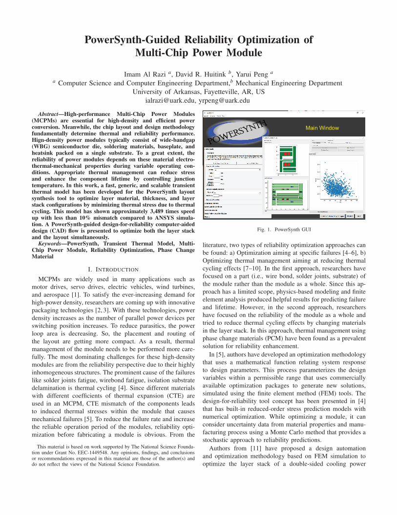
Main Window
Fig. 1. PowerSynth GUI
literature, two types of reliability optimization approaches can
be found: a) Optimization aiming at specific failures [4–6], b)
Optimizing thermal management aiming at reducing thermal
cycling effects [7–10]. In the first approach, researchers have
focused on a part (i.e., wire bond, solder joints, substrate) of
the module rather than the module as a whole. Since this ap-
proach has a limited scope, physics-based modeling and finite
element analysis produced helpful results for predicting failure
and lifetime. However, in the second approach, researchers
have focused on the reliability of the module as a whole and
tried to reduce thermal cycling effects by changing materials
in the layer stack. In this approach, thermal management using
phase change materials (PCM) have been found as a prevalent
solution for reliability enhancement.
In [5], authors have developed an optimization methodology
that uses a mathematical function relating system response
to design parameters. This process parameterizes the design
variables within a permissible range that uses commercially
available optimization packages to generate new solutions,
simulated using the finite element method (FEM) tools. The
design-for-reliability tool concept has been presented in [4]
that has built-in reduced-order stress prediction models with
numerical optimization. While optimizing a module, it can
consider uncertainty data from material properties and manu-
facturing process using a Monte Carlo method that provides a
stochastic approach to reliability predictions.
Authors from [11] have proposed a design automation
and optimization methodology based on FEM simulation to
optimize the layer stack of a double-sided cooling power
Post-Layout Optimization
MCPM Input Manufacturer
Design Kit (MDK)Layer Stack
Construction
Hierarchical,
Constraint-Aware
Layout Engine
Mechanical
(Stress Reliability)
API
(External
Models/Tools)
Complete
Solution Space
Export to 3D
CAD Tools
Netlist
Extraction
Solution Export
Design Modeling
Initial Layout
Geometry Script
Electrical (Parasitics, EMI)
Thermal (Static, Transient)
Pareto-front
Solution Set
Filleting Sharp
Corner
Solution Browser & Post-Optimization
Layout Generation
Multi-Objective Optimization
Fig. 2. PowerSynth architecture
module. Several research groups have identified PCMs as an
effective ingredient of the power module layer stack that acts
as buffers against the intermittent temperature spikes from
thermal cycling. In [9, 10], authors have used PCM to reduce
the peak temperature of the module under thermal cycling.
In [8], authors have shown that PCM can be modeled as
voltage-controlled variable RC-network and verified benefits
of using PCM over encapsulant using such a network model.
However, a few drawbacks exist with the aforementioned
approaches, like the limited solution space from the parame-
terized approach and the requirements of customized models
for different failure mechanisms. Besides, no prior work has
considered the layout placement and routing impact as all
methods involve highly time-consuming FEM simulations. A
multi-objective optimization tool for MCPM layout design
automation called PowerSynth [12] (graphical user interface
shown in Fig. 1) has been introduced to optimize device
placement and trace routing of the traces based on electro-
thermal tradeoff. Reduced-order thermal and electrical models
are used to predict the static maximum temperature and loop
inductance of a solution layout, assuming a fixed layer stack.
In [13], the authors have shown significant improvement in
the layout generation algorithms compared to the previous
work [12]. A hardware validation of PowerSynth optimization
results is performed through a 2.5D power module, and the
optimization objective includes the static maximum junction
temperature. The thermal model used in both works has
been validated against experimental measurements for static
temperature evaluation only. This model cannot account for
transient thermal cycling, which is the missing piece from the
tool to be capable of performing reliability optimization.
In this work, the key contributions are: (1) A fast transient
thermal model to evaluate maximum, average, and peak-to-
peak temperature of a module for a given thermal cycling
waveform; (2) A reliability optimization methodology that
suggests not only an optimum layer stack but also balanced
layouts for electro-thermal reliability; (3) A comparative study
of using PCM to control temperature variation and reduce
thermal cycling stress. This model can predict both static and
transient thermal performance, including PCM in the layer
stack. In contrast, the previous PowerSynth model can only
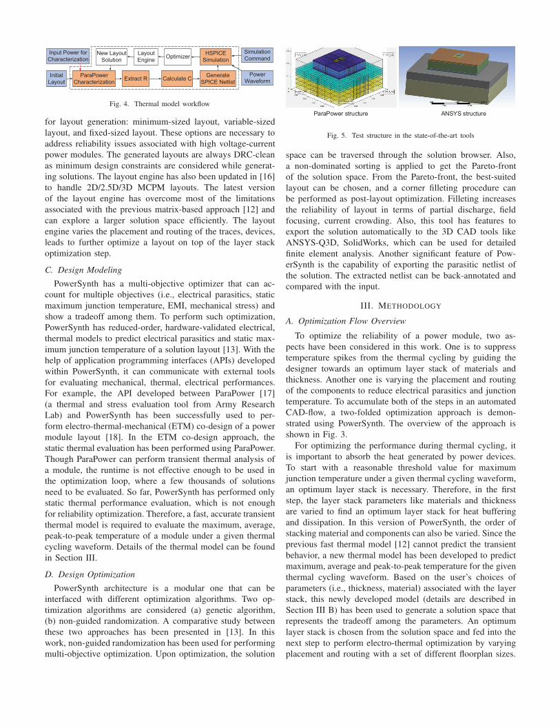
Output
Input
Waveform
Initial Layer
Stack & Design
Parameters
Parameterized
Layer Stacks
Thermal
Model
Find
Optimum
Layer Stack
Layout
Engine
Input
Layout
Solution
Layout
Performance
Evaluation Models
Optimizer
Pareto-front
solution set
Export
SolutionDone
?
Y
NStep-1
Step-2
Fig. 3. Two-step optimization flow
predict static thermal performance for a fixed layer stack with
only non-PCM. The thermal model has been developed within
the PowerSynth to leverage the built-in electrical model for
electrical reliability optimization. A case study using a half-
bridge MCPM is demonstrated to prove the efficiency of the
methodology.
The rest of the paper is organized as follows: Section
II describes an overview of the PowerSynth CAD-flow. In
Section III, the transient thermal model along with the reli-
ability optimization methodology is presented. An efficiency
comparison of the proposed thermal model with the state-of-
the-art tools is also demonstrated with the model validation
results. The reliability optimization results with a case study
are presented in Section IV. Finally, Section V concludes the
paper with a plan for future work.
II. POWERSYNTH OVERVIEW
PowerSynth [12] is the first CAD tool that performs multi-
objective optimization of a multi-chip power module and
suggests a Pareto-front solution space. An overview of Pow-
erSynth architecture is shown in Figure. 2 with the entire
package released at [14]. A brief description of each block
is provided below.
A. MCPM Input
The tool has a built-in manufacturer design kit (MDK) that
contains information about components, material properties,
and dimensions for power devices, substrates, connectors,
heat spreaders, wire bonds, and leads. Also, a set of design
constraints is required to ensure the solutions design rule
check (DRC) clean. To gather the geometrical and connectivity
information, our tool takes a layout script as input. The layout
script and MDK together are considered to create the layer
stack of the whole module. In [12], the number of layers is
fixed and the order cannot be altered. Only the placement
and routing of the traces and devices are permitted during
optimization. However, for reliability optimization, the layer
stack is a significant part, which needs to be generalized
with unlimited layers. Therefore, in this work the layer stack
handling approach has been updated to consider the order and
number of layers.
B. Layout Generation
A constraint-aware layout engine is developed using a hi-
erarchical corner stitch tree with the constraint graph method-
ology. The engine can handle layouts with heterogeneous
components and arbitrary Manhattan geometry. The algorithms
to honor both design and reliability constraints are shown to be
efficient [15]. To improve flexibility, there are a few choices
ParaPower
CharacterizationExtract R Calculate C
Generate
SPICE Netlist
HSPICE
Simulation
Power
Waveform
Simulation
CommandOptimizerLayout
Engine
New Layout
Solution
Initial
Layout
Input Power for
Characterization
Fig. 4. Thermal model workflow
for layout generation: minimum-sized layout, variable-sized
layout, and fixed-sized layout. These options are necessary to
address reliability issues associated with high voltage-current
power modules. The generated layouts are always DRC-clean
as minimum design constraints are considered while generat-
ing solutions. The layout engine has also been updated in [16]
to handle 2D/2.5D/3D MCPM layouts. The latest version
of the layout engine has overcome most of the limitations
associated with the previous matrix-based approach [12] and
can explore a larger solution space efficiently. The layout
engine varies the placement and routing of the traces, devices,
leads to further optimize a layout on top of the layer stack
optimization step.
C. Design Modeling
PowerSynth has a multi-objective optimizer that can ac-
count for multiple objectives (i.e., electrical parasitics, static
maximum junction temperature, EMI, mechanical stress) and
show a tradeoff among them. To perform such optimization,
PowerSynth has reduced-order, hardware-validated electrical,
thermal models to predict electrical parasitics and static max-
imum junction temperature of a solution layout [13]. With the
help of application programming interfaces (APIs) developed
within PowerSynth, it can communicate with external tools
for evaluating mechanical, thermal, electrical performances.
For example, the API developed between ParaPower [17]
(a thermal and stress evaluation tool from Army Research
Lab) and PowerSynth has been successfully used to per-
form electro-thermal-mechanical (ETM) co-design of a power
module layout [18]. In the ETM co-design approach, the
static thermal evaluation has been performed using ParaPower.
Though ParaPower can perform transient thermal analysis of
a module, the runtime is not effective enough to be used in
the optimization loop, where a few thousands of solutions
need to be evaluated. So far, PowerSynth has performed only
static thermal performance evaluation, which is not enough
for reliability optimization. Therefore, a fast, accurate transient
thermal model is required to evaluate the maximum, average,
peak-to-peak temperature of a module under a given thermal
cycling waveform. Details of the thermal model can be found
in Section III.
D. Design Optimization
PowerSynth architecture is a modular one that can be
interfaced with different optimization algorithms. Two op-
timization algorithms are considered (a) genetic algorithm,
(b) non-guided randomization. A comparative study between
these two approaches has been presented in [13]. In this
work, non-guided randomization has been used for performing
multi-objective optimization. Upon optimization, the solution
ParaPower structure ANSYS structure
Fig. 5. Test structure in the state-of-the-art tools
space can be traversed through the solution browser. Also,
a non-dominated sorting is applied to get the Pareto-front
of the solution space. From the Pareto-front, the best-suited
layout can be chosen, and a corner filleting procedure can
be performed as post-layout optimization. Filleting increases
the reliability of layout in terms of partial discharge, field
focusing, current crowding. Also, this tool has features to
export the solution automatically to the 3D CAD tools like
ANSYS-Q3D, SolidWorks, which can be used for detailed
finite element analysis. Another significant feature of Pow-
erSynth is the capability of exporting the parasitic netlist of
the solution. The extracted netlist can be back-annotated and
compared with the input.
III. METHODOLOGY
A. Optimization Flow Overview
To optimize the reliability of a power module, two as-
pects have been considered in this work. One is to suppress
temperature spikes from the thermal cycling by guiding the
designer towards an optimum layer stack of materials and
thickness. Another one is varying the placement and routing
of the components to reduce electrical parasitics and junction
temperature. To accumulate both of the steps in an automated
CAD-flow, a two-folded optimization approach is demon-
strated using PowerSynth. The overview of the approach is
shown in Fig. 3.
For optimizing the performance during thermal cycling, it
is important to absorb the heat generated by power devices.
To start with a reasonable threshold value for maximum
junction temperature under a given thermal cycling waveform,
an optimum layer stack is necessary. Therefore, in the first
step, the layer stack parameters like materials and thickness
are varied to find an optimum layer stack for heat buffering
and dissipation. In this version of PowerSynth, the order of
stacking material and components can also be varied. Since the
previous fast thermal model [12] cannot predict the transient
behavior, a new thermal model has been developed to predict
maximum, average and peak-to-peak temperature for the given
thermal cycling waveform. Based on the user’s choices of
parameters (i.e., thickness, material) associated with the layer
stack, this newly developed model (details are described in
Section III B) has been used to generate a solution space that
represents the tradeoff among the parameters. An optimum
layer stack is chosen from the solution space and fed into the
next step to perform electro-thermal optimization by varying
placement and routing with a set of different floorplan sizes.
V
20
Die1
80
Die2
80
C
0.0186
C
0.0186
R
0.1742
R
0.1742
C2.187
R
0.20075
C
10.8558
R
0.162
C
2.187
R
0.02375
C
43.3875
R
0.06055
C
C_s,C_tr,C_l
R
R_s,R_tr,R_l
Rdie1
Rs,Rtr,Rl
Cs,Ctr,Cl
Cdie1
Rdie2
Cdie2 Cmetal1
Rmetal1 Rceramic
Cceramic Cmetal
Rmetal Rbase
Cbase
Rpcm
CpcmVamb
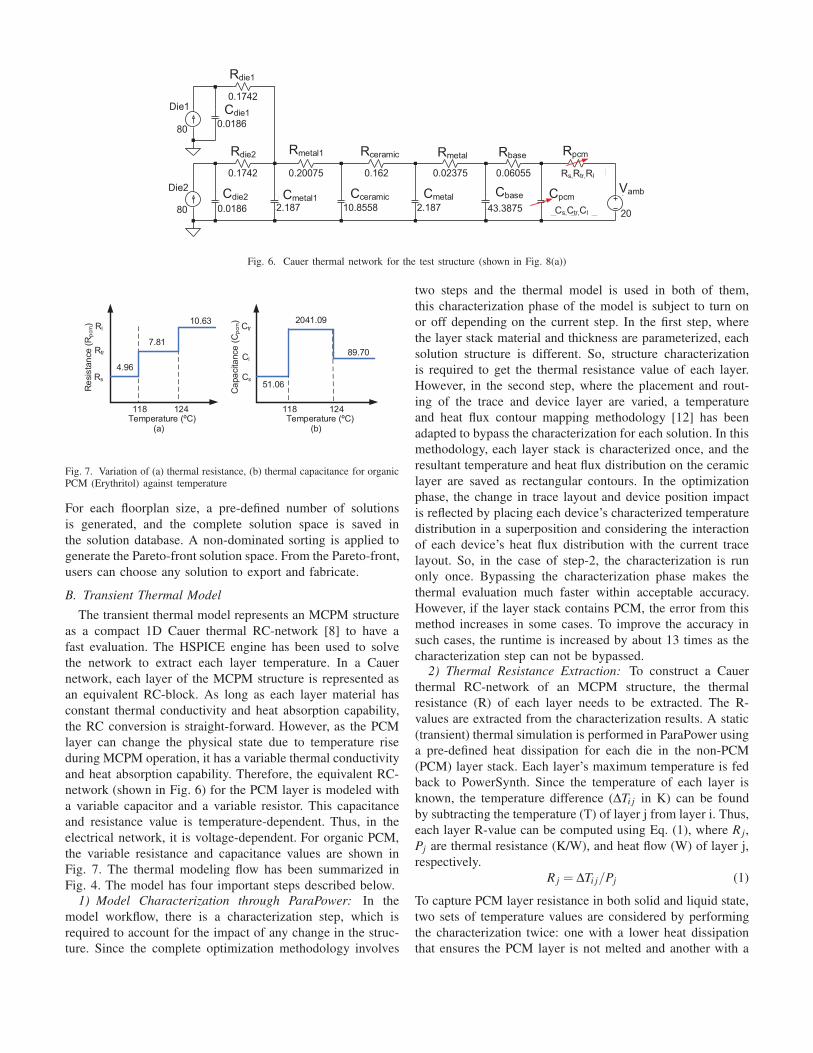
Fig. 6. Cauer thermal network for the test structure (shown in Fig. 8(a))
4.96
e
cn
atsi
se
R(R
pcm)
Temperature (ºC)
Rs
Rl
Rtr
7.81
118 124
10.63
51.06
Ca
pa
cita
nce
(C
pcm)
Temperature (ºC)
Cs
Ctr
Cl
2041.09
118 124
89.70
(b)(a)
Fig. 7. Variation of (a) thermal resistance, (b) thermal capacitance for organicPCM (Erythritol) against temperature
For each floorplan size, a pre-defined number of solutions
is generated, and the complete solution space is saved in
the solution database. A non-dominated sorting is applied to
generate the Pareto-front solution space. From the Pareto-front,
users can choose any solution to export and fabricate.
B. Transient Thermal Model
The transient thermal model represents an MCPM structure
as a compact 1D Cauer thermal RC-network [8] to have a
fast evaluation. The HSPICE engine has been used to solve
the network to extract each layer temperature. In a Cauer
network, each layer of the MCPM structure is represented as
an equivalent RC-block. As long as each layer material has
constant thermal conductivity and heat absorption capability,
the RC conversion is straight-forward. However, as the PCM
layer can change the physical state due to temperature rise
during MCPM operation, it has a variable thermal conductivity
and heat absorption capability. Therefore, the equivalent RC-
network (shown in Fig. 6) for the PCM layer is modeled with
a variable capacitor and a variable resistor. This capacitance
and resistance value is temperature-dependent. Thus, in the
electrical network, it is voltage-dependent. For organic PCM,
the variable resistance and capacitance values are shown in
Fig. 7. The thermal modeling flow has been summarized in
Fig. 4. The model has four important steps described below.
1) Model Characterization through ParaPower: In the
model workflow, there is a characterization step, which is
required to account for the impact of any change in the struc-
ture. Since the complete optimization methodology involves
two steps and the thermal model is used in both of them,
this characterization phase of the model is subject to turn on
or off depending on the current step. In the first step, where
the layer stack material and thickness are parameterized, each
solution structure is different. So, structure characterization
is required to get the thermal resistance value of each layer.
However, in the second step, where the placement and rout-
ing of the trace and device layer are varied, a temperature
and heat flux contour mapping methodology [12] has been
adapted to bypass the characterization for each solution. In this
methodology, each layer stack is characterized once, and the
resultant temperature and heat flux distribution on the ceramic
layer are saved as rectangular contours. In the optimization
phase, the change in trace layout and device position impact
is reflected by placing each device’s characterized temperature
distribution in a superposition and considering the interaction
of each device’s heat flux distribution with the current trace
layout. So, in the case of step-2, the characterization is run
only once. Bypassing the characterization phase makes the
thermal evaluation much faster within acceptable accuracy.
However, if the layer stack contains PCM, the error from this
method increases in some cases. To improve the accuracy in
such cases, the runtime is increased by about 13 times as the
characterization step can not be bypassed.2) Thermal Resistance Extraction: To construct a Cauer
thermal RC-network of an MCPM structure, the thermal
resistance (R) of each layer needs to be extracted. The R-
values are extracted from the characterization results. A static
(transient) thermal simulation is performed in ParaPower using
a pre-defined heat dissipation for each die in the non-PCM
(PCM) layer stack. Each layer’s maximum temperature is fed
back to PowerSynth. Since the temperature of each layer is
known, the temperature difference (∆Ti j in K) can be found
by subtracting the temperature (T) of layer j from layer i. Thus,
each layer R-value can be computed using Eq. (1), where R j,
Pj are thermal resistance (K/W), and heat flow (W) of layer j,
respectively.
R j = ∆Ti j/Pj (1)
To capture PCM layer resistance in both solid and liquid state,
two sets of temperature values are considered by performing
the characterization twice: one with a lower heat dissipation
that ensures the PCM layer is not melted and another with a
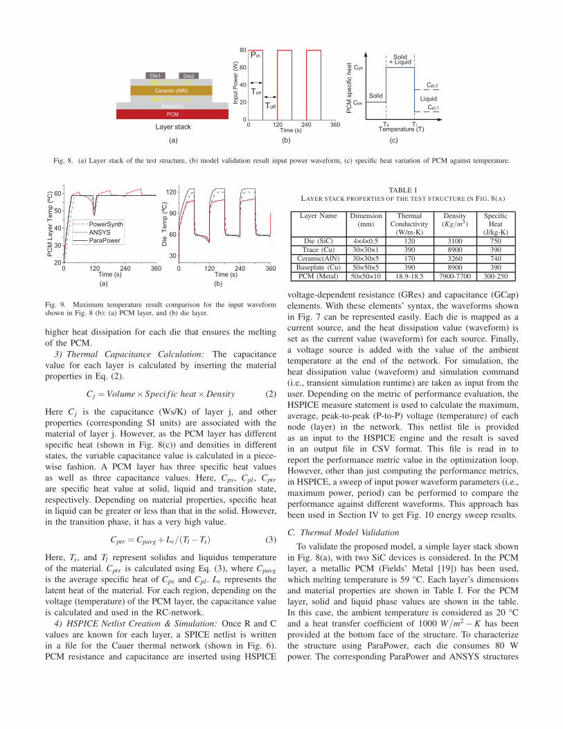
Layer stack
(a) (b) (c)
Die1 Die2
Metal Trace1 (Cu)
Ceramic (AlN)
Base(Cu)
PCM
Metal Trace (Cu)Solid Liquid
PC
M s
pe
cific
hea
t
Temperature (T)
Cps
Cptr
Cpl,1
Cpl,2
Solid+ Liquid
Ts Tl
Ton
Toff
0 120 240 3600
20
40
60
80
)W( r
ew
oP t
up
nI
Time (s)
Pm
Fig. 8. (a) Layer stack of the test structure, (b) model validation result input power waveform, (c) specific heat variation of PCM against temperature.
(a) (b)
0 120 240 360
30
60
90
120
( p
me
T ei
D)
C
Time (s)0 120 240 360
20
30
40
50
60
( p
me
T re
ya
L M
CP
)C
Time (s)
PowerSynth
ANSYS
ParaPower
°°
Fig. 9. Maximum temperature result comparison for the input waveformshown in Fig. 8 (b): (a) PCM layer, and (b) die layer.
higher heat dissipation for each die that ensures the melting
of the PCM.
3) Thermal Capacitance Calculation: The capacitance
value for each layer is calculated by inserting the material
properties in Eq. (2).
C j =Volume× Speci f ic heat ×Density (2)
Here C j is the capacitance (Ws/K) of layer j, and other
properties (corresponding SI units) are associated with the
material of layer j. However, as the PCM layer has different
specific heat (shown in Fig. 8(c)) and densities in different
states, the variable capacitance value is calculated in a piece-
wise fashion. A PCM layer has three specific heat values
as well as three capacitance values. Here, Cps, Cpl , Cptr
are specific heat value at solid, liquid and transition state,
respectively. Depending on material properties, specific heat
in liquid can be greater or less than that in the solid. However,
in the transition phase, it has a very high value.
Cptr =Cpavg +Lv/(Tl −Ts) (3)
Here, Ts, and Tl represent solidus and liquidus temperature
of the material. Cptr is calculated using Eq. (3), where Cpavg
is the average specific heat of Cps and Cpl . Lv represents the
latent heat of the material. For each region, depending on the
voltage (temperature) of the PCM layer, the capacitance value
is calculated and used in the RC-network.
4) HSPICE Netlist Creation & Simulation: Once R and C
values are known for each layer, a SPICE netlist is written
in a file for the Cauer thermal network (shown in Fig. 6).
PCM resistance and capacitance are inserted using HSPICE
TABLE ILAYER STACK PROPERTIES OF THE TEST STRUCTURE IN FIG. 8(A)
Layer Name Dimension(mm)
ThermalConductivity
(W/m-K)
Density(Kg/m3)
SpecificHeat
(J/kg-K)
Die (SiC) 4×4×0.5 120 3100 750
Trace (Cu) 30×30×1 390 8900 390
Ceramic(AlN) 30×30×5 170 3260 740
Baseplate (Cu) 50×50×5 390 8900 390
PCM (Metal) 50×50×10 18.9-18.5 7900-7700 300-250
voltage-dependent resistance (GRes) and capacitance (GCap)
elements. With these elements’ syntax, the waveforms shown
in Fig. 7 can be represented easily. Each die is mapped as a
current source, and the heat dissipation value (waveform) is
set as the current value (waveform) for each source. Finally,
a voltage source is added with the value of the ambient
temperature at the end of the network. For simulation, the
heat dissipation value (waveform) and simulation command
(i.e., transient simulation runtime) are taken as input from the
user. Depending on the metric of performance evaluation, the
HSPICE measure statement is used to calculate the maximum,
average, peak-to-peak (P-to-P) voltage (temperature) of each
node (layer) in the network. This netlist file is provided
as an input to the HSPICE engine and the result is saved
in an output file in CSV format. This file is read in to
report the performance metric value in the optimization loop.
However, other than just computing the performance metrics,
in HSPICE, a sweep of input power waveform parameters (i.e.,
maximum power, period) can be performed to compare the
performance against different waveforms. This approach has
been used in Section IV to get Fig. 10 energy sweep results.
C. Thermal Model Validation
To validate the proposed model, a simple layer stack shown
in Fig. 8(a), with two SiC devices is considered. In the PCM
layer, a metallic PCM (Fields’ Metal [19]) has been used,
which melting temperature is 59 °C. Each layer’s dimensions
and material properties are shown in Table I. For the PCM
layer, solid and liquid phase values are shown in the table.
In this case, the ambient temperature is considered as 20 °C
and a heat transfer coefficient of 1000 W/m2−K has been
provided at the bottom face of the structure. To characterize
the structure using ParaPower, each die consumes 80 W
power. The corresponding ParaPower and ANSYS structures
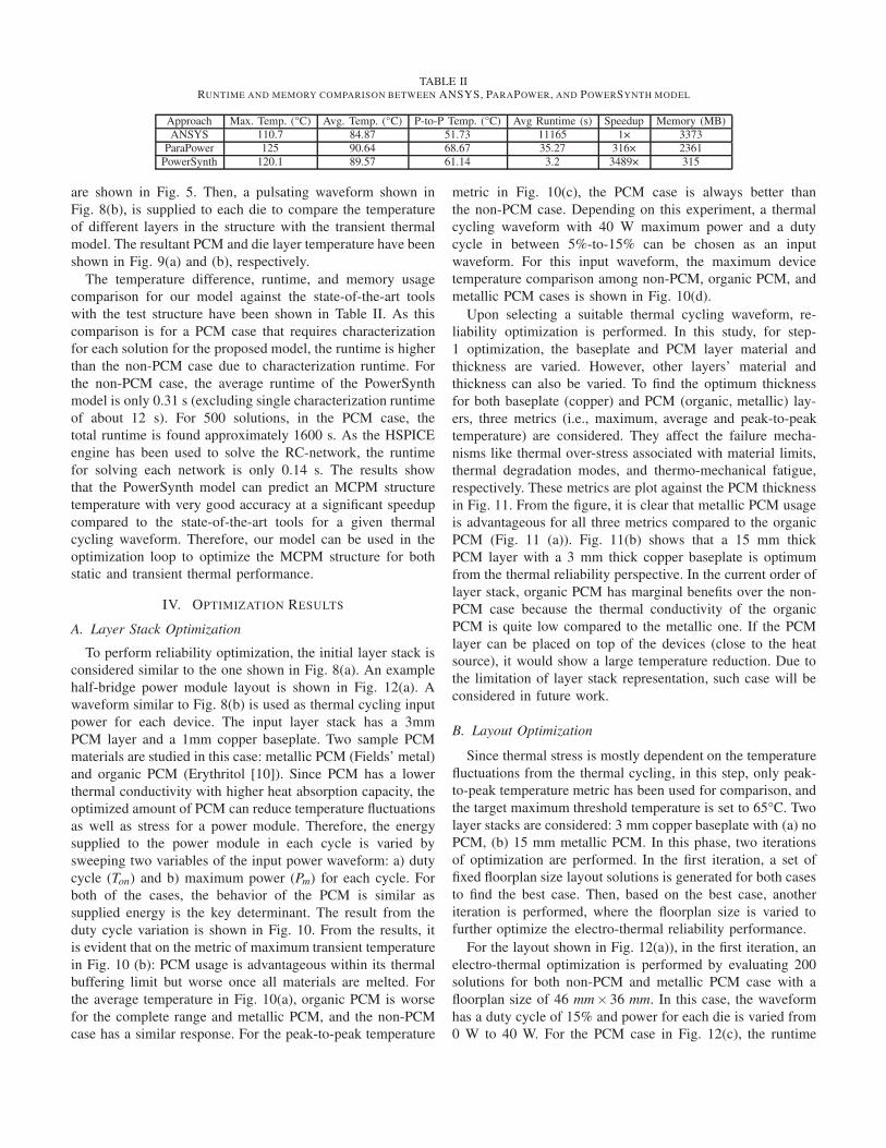
TABLE IIRUNTIME AND MEMORY COMPARISON BETWEEN ANSYS, PARAPOWER, AND POWERSYNTH MODEL
Approach Max. Temp. (°C) Avg. Temp. (°C) P-to-P Temp. (°C) Avg Runtime (s) Speedup Memory (MB)
ANSYS 110.7 84.87 51.73 11165 1× 3373
ParaPower 125 90.64 68.67 35.27 316× 2361
PowerSynth 120.1 89.57 61.14 3.2 3489× 315
are shown in Fig. 5. Then, a pulsating waveform shown in
Fig. 8(b), is supplied to each die to compare the temperature
of different layers in the structure with the transient thermal
model. The resultant PCM and die layer temperature have been
shown in Fig. 9(a) and (b), respectively.
The temperature difference, runtime, and memory usage
comparison for our model against the state-of-the-art tools
with the test structure have been shown in Table II. As this
comparison is for a PCM case that requires characterization
for each solution for the proposed model, the runtime is higher
than the non-PCM case due to characterization runtime. For
the non-PCM case, the average runtime of the PowerSynth
model is only 0.31 s (excluding single characterization runtime
of about 12 s). For 500 solutions, in the PCM case, the
total runtime is found approximately 1600 s. As the HSPICE
engine has been used to solve the RC-network, the runtime
for solving each network is only 0.14 s. The results show
that the PowerSynth model can predict an MCPM structure
temperature with very good accuracy at a significant speedup
compared to the state-of-the-art tools for a given thermal
cycling waveform. Therefore, our model can be used in the
optimization loop to optimize the MCPM structure for both
static and transient thermal performance.
IV. OPTIMIZATION RESULTS
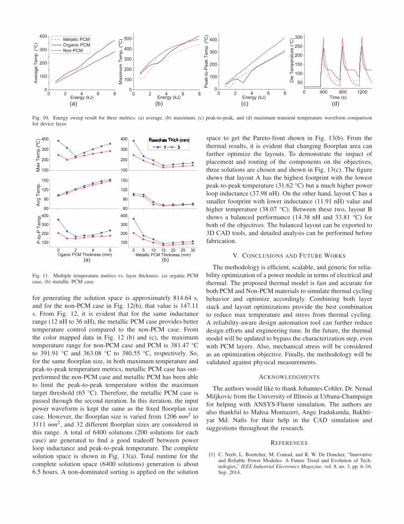
A. Layer Stack Optimization
To perform reliability optimization, the initial layer stack is
considered similar to the one shown in Fig. 8(a). An example
half-bridge power module layout is shown in Fig. 12(a). A
waveform similar to Fig. 8(b) is used as thermal cycling input
power for each device. The input layer stack has a 3mm
PCM layer and a 1mm copper baseplate. Two sample PCM
materials are studied in this case: metallic PCM (Fields’ metal)
and organic PCM (Erythritol [10]). Since PCM has a lower
thermal conductivity with higher heat absorption capacity, the
optimized amount of PCM can reduce temperature fluctuations
as well as stress for a power module. Therefore, the energy
supplied to the power module in each cycle is varied by
sweeping two variables of the input power waveform: a) duty
cycle (Ton) and b) maximum power (Pm) for each cycle. For
both of the cases, the behavior of the PCM is similar as
supplied energy is the key determinant. The result from the
duty cycle variation is shown in Fig. 10. From the results, it
is evident that on the metric of maximum transient temperature
in Fig. 10 (b): PCM usage is advantageous within its thermal
buffering limit but worse once all materials are melted. For
the average temperature in Fig. 10(a), organic PCM is worse
for the complete range and metallic PCM, and the non-PCM
case has a similar response. For the peak-to-peak temperature
metric in Fig. 10(c), the PCM case is always better than
the non-PCM case. Depending on this experiment, a thermal
cycling waveform with 40 W maximum power and a duty
cycle in between 5%-to-15% can be chosen as an input
waveform. For this input waveform, the maximum device
temperature comparison among non-PCM, organic PCM, and
metallic PCM cases is shown in Fig. 10(d).
Upon selecting a suitable thermal cycling waveform, re-
liability optimization is performed. In this study, for step-
1 optimization, the baseplate and PCM layer material and
thickness are varied. However, other layers’ material and
thickness can also be varied. To find the optimum thickness
for both baseplate (copper) and PCM (organic, metallic) lay-
ers, three metrics (i.e., maximum, average and peak-to-peak
temperature) are considered. They affect the failure mecha-
nisms like thermal over-stress associated with material limits,
thermal degradation modes, and thermo-mechanical fatigue,
respectively. These metrics are plot against the PCM thickness
in Fig. 11. From the figure, it is clear that metallic PCM usage
is advantageous for all three metrics compared to the organic
PCM (Fig. 11 (a)). Fig. 11(b) shows that a 15 mm thick
PCM layer with a 3 mm thick copper baseplate is optimum
from the thermal reliability perspective. In the current order of
layer stack, organic PCM has marginal benefits over the non-
PCM case because the thermal conductivity of the organic
PCM is quite low compared to the metallic one. If the PCM
layer can be placed on top of the devices (close to the heat
source), it would show a large temperature reduction. Due to
the limitation of layer stack representation, such case will be
considered in future work.
B. Layout Optimization
Since thermal stress is mostly dependent on the temperature
fluctuations from the thermal cycling, in this step, only peak-
to-peak temperature metric has been used for comparison, and
the target maximum threshold temperature is set to 65°C. Two
layer stacks are considered: 3 mm copper baseplate with (a) no
PCM, (b) 15 mm metallic PCM. In this phase, two iterations
of optimization are performed. In the first iteration, a set of
fixed floorplan size layout solutions is generated for both cases
to find the best case. Then, based on the best case, another
iteration is performed, where the floorplan size is varied to
further optimize the electro-thermal reliability performance.
For the layout shown in Fig. 12(a)), in the first iteration, an
electro-thermal optimization is performed by evaluating 200
solutions for both non-PCM and metallic PCM case with a
floorplan size of 46 mm× 36 mm. In this case, the waveform
has a duty cycle of 15% and power for each die is varied from
0 W to 40 W. For the PCM case in Fig. 12(c), the runtime
(a) (c)
0 2 4 6 80
100
200
300
400
500
( .p
me
T m
umi
xa
M)
C
Energy (kJ)
(b) (d)
0 2 4 6 80
100
200
300
400
( .p
me
T k
ae
P-ot-
ka
eP
)C
Energy (kJ)
°°
Fig. 10. Energy sweep result for three metrics: (a) average, (b) maximum, (c) peak-to-peak, and (d) maximum transient temperature waveform comparisonfor device layer.
(a) (b)
P-t
o-
pm
eT
P.
p
me
T g
vA
.p
me
T x
aM
.(⁰C
)
Fig. 11. Multiple temperature metrics vs. layer thickness: (a) organic PCMcase, (b) metallic PCM case.
for generating the solution space is approximately 814.64 s,
and for the non-PCM case in Fig. 12(b), that value is 147.11
s. From Fig. 12, it is evident that for the same inductance
range (12 nH to 36 nH), the metallic PCM case provides better
temperature control compared to the non-PCM case. From
the color mapped data in Fig. 12 (b) and (c), the maximum
temperature range for non-PCM case and PCM is 381.47 °C
to 391.91 °C and 363.08 °C to 380.55 °C, respectively. So,
for the same floorplan size, in both maximum temperature and
peak-to-peak temperature metrics, metallic PCM case has out-
performed the non-PCM case and metallic PCM has been able
to limit the peak-to-peak temperature within the maximum
target threshold (65 °C). Therefore, the metallic PCM case is
passed through the second iteration. In this iteration, the input
power waveform is kept the same as the fixed floorplan size
case. However, the floorplan size is varied from 1206 mm2 to
3111 mm2, and 32 different floorplan sizes are considered in
this range. A total of 6400 solutions (200 solutions for each
case) are generated to find a good tradeoff between power
loop inductance and peak-to-peak temperature. The complete
solution space is shown in Fig. 13(a). Total runtime for the
complete solution space (6400 solutions) generation is about
6.5 hours. A non-dominated sorting is applied on the solution
space to get the Pareto-front shown in Fig. 13(b). From the
thermal results, it is evident that changing floorplan area can
further optimize the layouts. To demonstrate the impact of
placement and routing of the components on the objectives,
three solutions are chosen and shown in Fig. 13(c). The figure
shows that layout A has the highest footprint with the lowest
peak-to-peak temperature (31.62 °C) but a much higher power
loop inductance (37.98 nH). On the other hand, layout C has a
smaller footprint with lower inductance (11.91 nH) value and
higher temperature (38.07 °C). Between these two, layout B
shows a balanced performance (14.38 nH and 33.81 °C) for
both of the objectives. The balanced layout can be exported to
3D CAD tools, and detailed analysis can be performed before
fabrication.
V. CONCLUSIONS AND FUTURE WORKS
The methodology is efficient, scalable, and generic for relia-
bility optimization of a power module in terms of electrical and
thermal. The proposed thermal model is fast and accurate for
both PCM and Non-PCM materials to simulate thermal cycling
behavior and optimize accordingly. Combining both layer
stack and layout optimizations provide the best combination
to reduce max temperature and stress from thermal cycling.
A reliability-aware design automation tool can further reduce
design efforts and engineering time. In the future, the thermal
model will be updated to bypass the characterization step, even
with PCM layers. Also, mechanical stress will be considered
as an optimization objective. Finally, the methodology will be
validated against physical measurements.
ACKNOWLEDGMENTS
The authors would like to thank Johannes Cohler, Dr. Nenad
Miljkovic from the University of Illinois at Urbana-Champaign
for helping with ANSYS-Fluent simulation. The authors are
also thankful to Mahsa Montazeri, Ange Iradukunda, Bakhti-
yar Md. Nafis for their help in the CAD simulation and
suggestions throughout the research.
REFERENCES
[1] C. Neeb, L. Boettcher, M. Conrad, and R. W. De Doncker, “Innovativeand Reliable Power Modules: A Future Trend and Evolution of Tech-nologies,” IEEE Industrial Electronics Magazine, vol. 8, no. 3, pp. 6–16,Sep. 2014.
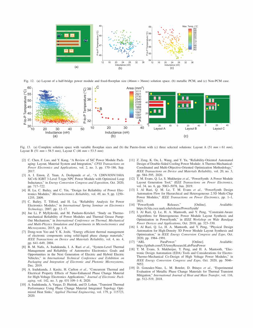
(c)(b)(a)
DC+
DC-
Out
Fig. 12. (a) Layout of a half-bridge power module and fixed-floorplan size (46mm×36mm) solution space. (b) metallic PCM, and (c) Non-PCM case.
(a) (b) (c)
A
B
C
0 20 40
40
60
20
20 400 20 4000
Layout A Layout B Layout C
Fig. 13. (a) Complete solution space with variable floorplan sizes and (b) the Pareto-front with (c) three selected solutions: Layout A (51 mm× 61 mm),Layout B (51 mm×58.5 mm), Layout C (46 mm×53.5 mm)
[2] C. Chen, F. Luo, and Y. Kang, “A Review of SiC Power Module Pack-aging: Layout, Material System and Integration,” CPSS Transactions on
Power Electronics and Applications, vol. 2, no. 3, pp. 170–186, Sep.2017.
[3] A. I. Emon, Z. Yuan, A. Deshpande et al., “A 1200V/650V/160ASiC+Si IGBT 3-Level T-type NPC Power Module with Optimized LoopInductance,” in Energy Conversion Congress and Exposition, Oct. 2020,pp. 717–722.
[4] H. Lu, C. Bailey, and C. Yin, “Design for Reliability of Power Elec-tronics Modules,” Microelectronics Reliability, vol. 49, no. 9, pp. 1250–1255, 2009.
[5] C. Bailey, T. Tilford, and H. Lu, “Reliability Analysis for PowerElectronics Modules,” in International Spring Seminar on Electronics
Technology, 2007, pp. 12–17.
[6] Jue Li, P. Myllykoski, and M. Paulasto-Krockel, “Study on Thermo-mechanical Reliability of Power Modules and Thermal Grease Pump-Out Mechanism,” in International Conference on Thermal, Mechanical
and Multi-Physics Simulation and Experiments in Microelectronics and
Microsystems, 2015, pp. 1–6.
[7] Dong-won Yoo and Y. K. Joshi, “Energy efficient thermal managementof electronic components using solid-liquid phase change materials,”IEEE Transactions on Device and Materials Reliability, vol. 4, no. 4,pp. 641–649, 2004.
[8] B. M. Nafis, A. Iradukunda, I. A. Razi et al., “System-Level ThermalManagement and Reliability of Automotive Electronics: Goals andOpportunities in the Next Generation of Electric and Hybrid ElectricVehicles,” in International Technical Conference and Exhibition on
Packaging and Integration of Electronic and Photonic Microsystems,Dec. 2019.
[9] A. Iradukunda, J. Kasitz, H. Carlton et al., “Concurrent Thermal andElectrical Property Effects of Nano-Enhanced Phase Change Materialfor High-Voltage Electronics Applications,” Journal of Electronic Pack-
aging, vol. 142, no. 3, pp. 031 109–1–8, 2020.
[10] A. Iradukunda, A. Vargas, D. Huitink, and D. Lohan, “Transient ThermalPerformance Using Phase Change Material Integrated Topology Opti-mized Heat Sinks,” Applied Thermal Engineering, vol. 179, p. 115723,2020.
[11] Z. Zeng, K. Ou, L. Wang, and Y. Yu, “Reliability-Oriented AutomatedDesign of Double-Sided Cooling Power Module: A Thermo-Mechanical-Coordinated and Multi-Objective-Oriented Optimization Methodology,”IEEE Transactions on Device and Materials Reliability, vol. 20, no. 3,pp. 584–595, 2020.
[12] T. M. Evans, Q. Le, S. Mukherjee et al., “PowerSynth: A Power ModuleLayout Generation Tool,” IEEE Transactions on Power Electronics,vol. 34, no. 6, pp. 5063–5078, Jun. 2019.
[13] I. Al Razi, Q. M. Le, T. M. Evans et al., “PowerSynth DesignAutomation Flow for Hierarchical and Heterogeneous 2.5D Multi-ChipPower Modules,” IEEE Transactions on Power Electronics, pp. 1–1,2021.
[14] “PowerSynth Releases.” [Online]. Available:https://e3da.csce.uark.edu/release/PowerSynth/
[15] I. Al Razi, Q. Le, H. A. Mantooth, and Y. Peng, “Constraint-AwareAlgorithms for Heterogeneous Power Module Layout Synthesis andOptimization in PowerSynth,” in IEEE Workshop on Wide Bandgap
Power Devices and Applications, Oct. 2018, pp. 323–330.[16] I. Al Razi, Q. Le, H. A. Mantooth, and Y. Peng, “Physical Design
Automation for High-Density 3D Power Module Layout Synthesis andOptimization,” in IEEE Energy Conversion Congress and Expo, Oct.2020, pp. 1984–1991.
[17] “ARL ParaPower.” [Online]. Available:https://github.com/USArmyResearchLab/ParaPower
[18] T. M. Evans, S. Mukherjee, Y. Peng, and H. A. Mantooth, “Elec-tronic Design Automation (EDA) Tools and Considerations for Electro-Thermo-Mechanical Co-Design of High Voltage Power Modules,” inIEEE Energy Conversion Congress and Expo, Oct. 2020, pp. 5046–5052.
[19] D. Gonzalez-Nino, L. M. Boteler, D. Ibitayo et al., “ExperimentalEvaluation of Metallic Phase Change Materials for Thermal TransientMitigation,” International Journal of Heat and Mass Transfer, vol. 116,pp. 512–519, 2018.