Embed Size (px)
Citation preview

On-Chip Network Designs for Many-Core Computational Platforms
By
ANH T. TRAN
B.S. (Posts and Telecommunications Institute of Technology, Hochiminh, Vietnam) 2003
M.S. (University of California, Davis, USA) 2009
DISSERTATION
Submitted in partial satisfaction of the requirements for the degree of
DOCTOR OF PHILOSOPHY
in
ELECTRICAL ENGINEERING
in the
OFFICE OF GRADUATE STUDIES
of the
UNIVERSITY OF CALIFORNIA
DAVIS
Approved:
Chair, Dr. Bevan M. Baas
Member, Dr. Kent Wilken
Member, Dr. Soheil Ghiasi
Committee in charge
2012
– i –

c© Copyright by Anh T. Tran 2012
All Rights Reserved

To my wife Khanh Nguyen, and our daughter Anh-My Tran
To my Parents
– ii –

Abstract
Processor designers have been utilizing more processing elements (PEs) on a single chip
to make efficient use of technology scaling and also to speed up system performance through in-
creased parallelism. Networks on-chip (NoCs) have been shown to be promising for scalable in-
terconnection of large numbers of PEs in comparison to structures such as point-to-point intercon-
nects or global buses. This dissertation investigates the designs of on-chip interconnection networks
for many-core computational platforms in three application domains: high-performance network
designs for applications with high communication bandwidths; low-cost networks for application-
specific low-bandwidth dynamic traffic; and reconfigurable networks for platforms targeting digital
signal processing (DSP) applications which have deterministic inter-task communication character-
istics.
An on-chip router architecture named RoShaQ is proposed for platforms executing general-
purpose applications with dynamic and high communication bandwidths. RoShaQ maximizes
buffer utilization by allowing sharing of multiple buffer queues among input ports hence achieves
high network performance. Experimental results show that RoShaQ is 17.2% lower latency, 18.2%
higher saturation throughput and 8.3% lower energy dissipated per bit than state-of-the-art virtual-
channel routers given the same buffer capacity averaged over a broad range of traffic patterns.
For mapping applications showing low inter-task communication bandwidths, five low-
cost bufferless routers are proposed. All routers guarantee in-order packet delivery so that expensive
reordering buffers are not required. The proposed bufferless routers have lower costs and higher
performance per unit cost than all buffered wormhole routers — the smallest proposed bufferless
router has 32.4% less area, 24.5% higher throughput, 29.5% lower latency, 10.0% lower power and
26.5% lower energy per bit than the smallest buffered router.
A globally asynchronous locally synchronous (GALS)-compatible reconfigurable circuit-
switched on-chip network is proposed for use in many-core platforms targeting streaming DSP and
embedded applications which show deterministic inter-task communication traffic. Inter-processor
communication is achieved through a simple yet effective source-synchronous technique which can
sustain the ideal throughput of one word per cycle and the ideal latency approaching the wire delay.
This network was utilized in a GALS many-core chip fabricated in 65 nm CMOS. For evaluating
– iii –
the efficiency of this platform, a complete IEEE 802.11a baseband receiver was implemented. The
receiver achieves a real-time throughput of 54 Mbps and consumes 174.8 mW with only 12.2 mW
(7.0%) dissipated by its interconnects.
A highly parameterizable NoC simulator named NoCTweak is also proposed for early
exploration of performance and energy efficiency of on-chip networks. The simulator has been
developed in SystemC, a C++ plugin, which allows fast modeling of concurrent hardware modules
at the cycle-level accuracy. Area, timing and power of router components are post-layout data based
on a 65 nm CMOS standard-cell library. NoCTweak was used in many experiments reported in this
dissertation.
– iv –

Acknowledgments
My journey as a PhD student at UC Davis is coming to an end; and now I am thinking back
to the many people who have supported me along the way. The journey has been full of learning
and growth, and I owe a great deal to the support and friendship of a large number of people who
have made this time so special and enriching.
First and foremost, I have the deepest gratitude to my advisor, Professor Bevan Baas.
Working under his supervision has been a true blessing, and I am grateful for all his guidance and
encouragement during my research. I have learned a great deal from him, not only in the field of my
research, but in many other ways as well. My work here has mostly benefited from his enthusiasm,
knowledge and constructive comments. I could not have hoped for a better advisor, and I will
forever be indebted to him.
I would like to thank Professor Kent Wilken and Professor Soheil Ghiasi for serving on my
doctoral committee and providing valuable feedback on this dissertation. I am grateful to Professor
Rajeevan Amirtharajah and Professor Matthew Farrens for evaluating my research proposal and
giving me useful directions so that I can fulfill my PhD program. I also would like to thank Professor
Anh-Vu Pham who helped me a lot when I started my graduate student life here at UC Davis.
I want to extend my appreciation to Dean, a great friend and also a co-author in my several
papers. I never forget the times we worked together like crazy in the last minutes before paper
submission deadlines. Those times were so painful but the rewards brought by paper acceptances
later made us hard to change that bad habit.
I also would like to thank past and current VCL lab members: Zhibin, Bin, Aaron, Jon,
Jeremy, Emmanuel, Brent, Micheal, Samir, Houshmand, Nima, Zhiyi, Tinoosh, Wayne, Trevin,
Stephen, Lucas, Henna. I have enjoyed many discussions with them on various topics and found
that there is always something I can learn from them.
I was so glad to have Ning working with me on the final project of the EEC116 VLSI
design class in Spring 2007. Chip layout with Magic was difficult but became much easier with him
along. Together, we won the first place in this class project which strongly encouraged me to pursue
my research in digital VLSI design.
– v –

Specially, I want to express my deep appreciation to my beloved wife Khanh, to whom
this dissertation is dedicated. Her constant love and tremendous support has allowed me to spend
most time and effort on this work. She also brought me the most wonderful gift, our lovely daughter
Amy.
I also want to thank all my friends and relatives who have helped and supported me during
my time here in Davis. They have turned my experience in Davis to be a memorable one.
My work done at UC Davis was supported by a Vietnam Education Foundation (VEF)
graduate fellowship, National Science Foundation (NSF) CAREER award No. 0546907, grants
CCF Grant No. 0903549 and CCF Grant No. 1018972, Semiconductor Research Corporation (SRC)
research grants GRC 1598.001, CSR 1659.001, and GRC 1971.001, C2S2 grant 2047.002.014,
ST Microelectronics CMOS standard-cell libraries and chip fabrication, UC Davis summer research
and conference travel awards, Intel and Intellasys grants.
– vi –

Contents
Abstract iii
Acknowledgments v
List of Figures x
List of Tables xiv
1 Introduction 1
1.1 The Era of Many-Core System Designs . . . . . . . . . . . . . . . . . . . . . . . 1
1.2 The Scope and Organization of this Dissertation . . . . . . . . . . . . . . . . . . . 3
2 Background, Related Work and Contributions 5
2.1 On-Chip Network Background . . . . . . . . . . . . . . . . . . . . . . . . . . . . 5
2.1.1 Network Topologies . . . . . . . . . . . . . . . . . . . . . . . . . . . . . 5
2.1.2 Data Transferring Techniques . . . . . . . . . . . . . . . . . . . . . . . . 8
2.1.3 Flow-Control Methods . . . . . . . . . . . . . . . . . . . . . . . . . . . . 9
2.1.4 Routing Strategies . . . . . . . . . . . . . . . . . . . . . . . . . . . . . . 10
2.1.5 Network Deadlock . . . . . . . . . . . . . . . . . . . . . . . . . . . . . . 11
2.1.6 Network Livelock . . . . . . . . . . . . . . . . . . . . . . . . . . . . . . 12
2.2 On-Chip Router Designs . . . . . . . . . . . . . . . . . . . . . . . . . . . . . . . 13
2.2.1 Basic Circuit Components of a Router . . . . . . . . . . . . . . . . . . . . 13
2.2.2 High-Performance Router Designs . . . . . . . . . . . . . . . . . . . . . . 15
2.2.3 Low-Cost Router Designs . . . . . . . . . . . . . . . . . . . . . . . . . . 16
2.3 Communication Methods for GALS Many-Core Systems . . . . . . . . . . . . . . 18
2.4 Contributions . . . . . . . . . . . . . . . . . . . . . . . . . . . . . . . . . . . . . 20
3 High-Performance On-Chip Networks with Shared-Queue Routers 22
3.1 Motivation . . . . . . . . . . . . . . . . . . . . . . . . . . . . . . . . . . . . . . . 23
3.1.1 Typical Router Architectures . . . . . . . . . . . . . . . . . . . . . . . . . 23
3.1.2 Opportunities for Achieving Higher Throughput . . . . . . . . . . . . . . 26
3.2 RoShaQ: Router Architecture with Shared Queues . . . . . . . . . . . . . . . . . . 27
3.2.1 The Initial Idea . . . . . . . . . . . . . . . . . . . . . . . . . . . . . . . . 27
3.2.2 RoShaQ Architecture . . . . . . . . . . . . . . . . . . . . . . . . . . . . . 29
3.2.3 RoShaQ Datapath Pipeline . . . . . . . . . . . . . . . . . . . . . . . . . . 30
3.2.4 Design of Allocators . . . . . . . . . . . . . . . . . . . . . . . . . . . . . 31
3.2.5 RoShaQ’s Properties . . . . . . . . . . . . . . . . . . . . . . . . . . . . . 33
– vii –

3.3 Experimental Results . . . . . . . . . . . . . . . . . . . . . . . . . . . . . . . . . 34
3.3.1 Experimental Setup . . . . . . . . . . . . . . . . . . . . . . . . . . . . . . 34
3.3.2 Latency and Throughput . . . . . . . . . . . . . . . . . . . . . . . . . . . 35
3.3.3 Power, Area and Energy . . . . . . . . . . . . . . . . . . . . . . . . . . . 40
3.4 Related Work . . . . . . . . . . . . . . . . . . . . . . . . . . . . . . . . . . . . . 43
3.5 Summary . . . . . . . . . . . . . . . . . . . . . . . . . . . . . . . . . . . . . . . 44
4 Low-Cost Router Designs with Guaranteed In-Order Packet Delivery 46
4.1 Conventional Wormhole Router Architecture and Cost Analysis . . . . . . . . . . 47
4.1.1 Wormhole Router Architecture . . . . . . . . . . . . . . . . . . . . . . . . 47
4.1.2 Performance Analysis and In-Order Packet Delivery . . . . . . . . . . . . 48
4.1.3 Area and Power Costs . . . . . . . . . . . . . . . . . . . . . . . . . . . . 49
4.2 Bufferless Packet-Switched Routers Providing In-Order Packet Delivery . . . . . . 51
4.2.1 Bufferless Router Architecture . . . . . . . . . . . . . . . . . . . . . . . . 51
4.2.2 Network Performance Analysis . . . . . . . . . . . . . . . . . . . . . . . 52
4.2.3 In-order Packet Delivery with Deterministic Routing . . . . . . . . . . . . 53
4.2.4 Adaptive Routing with ACK Controlling . . . . . . . . . . . . . . . . . . 53
4.2.5 Adaptive Routing with Packet Length Awareness (PLA) . . . . . . . . . . 54
4.3 Bufferless Circuit-Switched Routers . . . . . . . . . . . . . . . . . . . . . . . . . 55
4.3.1 Architecture . . . . . . . . . . . . . . . . . . . . . . . . . . . . . . . . . . 55
4.3.2 Performance Analysis and In-Order Packet Delivery . . . . . . . . . . . . 57
4.4 Experimental Results on Latency and Throughput . . . . . . . . . . . . . . . . . . 58
4.4.1 Performance Over Synthetic Traffic Patterns . . . . . . . . . . . . . . . . . 58
4.4.2 Performance Over Embedded Application Traffic Patterns . . . . . . . . . 65
4.5 Area, Power and Energy . . . . . . . . . . . . . . . . . . . . . . . . . . . . . . . 67
4.5.1 Evaluation Methodology . . . . . . . . . . . . . . . . . . . . . . . . . . . 67
4.5.2 Power and Energy over Synthetic Traffic Patterns . . . . . . . . . . . . . . 68
4.5.3 Power and Energy over Embedded Application Traces . . . . . . . . . . . 74
4.5.4 Comparative Analysis and Discussion . . . . . . . . . . . . . . . . . . . . 74
4.6 Related Work . . . . . . . . . . . . . . . . . . . . . . . . . . . . . . . . . . . . . 76
4.7 Summary . . . . . . . . . . . . . . . . . . . . . . . . . . . . . . . . . . . . . . . 78
5 A Reconfigurable Source-Synchronous On-Chip Network for GALS Many-Core Plat-
forms 79
5.1 Motivation For A GALS Many-Core Platform . . . . . . . . . . . . . . . . . . . . 80
5.1.1 High Performance with Many-Core Design . . . . . . . . . . . . . . . . . 80
5.1.2 Advantages of the GALS Clocking Style . . . . . . . . . . . . . . . . . . 80
5.2 Design and Evaluation of a Reconfigurable GALS-Compatible Source-Synchronous
On-Chip Network . . . . . . . . . . . . . . . . . . . . . . . . . . . . . . . . . . . 82
5.2.1 Architecture of Reconfigurable Interconnection Network . . . . . . . . . . 83
5.2.2 Approach Methodology . . . . . . . . . . . . . . . . . . . . . . . . . . . 85
5.2.3 Link and Device Delays . . . . . . . . . . . . . . . . . . . . . . . . . . . 85
5.2.4 Interconnect Throughput Evaluation . . . . . . . . . . . . . . . . . . . . . 89
5.2.5 Interconnect Latency . . . . . . . . . . . . . . . . . . . . . . . . . . . . . 91
5.2.6 Discussion . . . . . . . . . . . . . . . . . . . . . . . . . . . . . . . . . . 92
5.3 An Example GALS Many-core Platform: AsAP2 . . . . . . . . . . . . . . . . . . 93
5.3.1 Per-Processor Clock Frequency and Supply Voltage Configuration . . . . . 94
5.3.2 Source-Synchronous Interconnection Network . . . . . . . . . . . . . . . 96
– viii –
5.3.3 Platform Configuration, Programming and Testability . . . . . . . . . . . . 97
5.3.4 Chip Implementation . . . . . . . . . . . . . . . . . . . . . . . . . . . . . 97
5.3.5 Measurement Results . . . . . . . . . . . . . . . . . . . . . . . . . . . . . 98
5.4 Related Work . . . . . . . . . . . . . . . . . . . . . . . . . . . . . . . . . . . . . 101
5.5 Summary . . . . . . . . . . . . . . . . . . . . . . . . . . . . . . . . . . . . . . . 102
6 Application Mapping Case Study: 802.11a Baseband Receiver on AsAP2 104
6.1 Architecture of a Complete 802.11a Baseband Receiver . . . . . . . . . . . . . . . 105
6.2 Mapping the 802.11a Baseband Receiver on AsAP2 . . . . . . . . . . . . . . . . . 109
6.2.1 Programming Methodology . . . . . . . . . . . . . . . . . . . . . . . . . 109
6.2.2 Application Mapping . . . . . . . . . . . . . . . . . . . . . . . . . . . . . 110
6.2.3 Critical Data Path and Reception of Multiple Frames . . . . . . . . . . . . 113
6.3 Performance, Power Evaluation and Optimization . . . . . . . . . . . . . . . . . . 115
6.3.1 Performance Evaluation . . . . . . . . . . . . . . . . . . . . . . . . . . . 115
6.3.2 Power Consumption Estimation . . . . . . . . . . . . . . . . . . . . . . . 117
6.3.3 Power Optimization . . . . . . . . . . . . . . . . . . . . . . . . . . . . . 118
6.4 Measurement Results . . . . . . . . . . . . . . . . . . . . . . . . . . . . . . . . . 121
6.5 Summary . . . . . . . . . . . . . . . . . . . . . . . . . . . . . . . . . . . . . . . 122
7 Conclusion and Future Directions 123
7.1 Dissertation Summary . . . . . . . . . . . . . . . . . . . . . . . . . . . . . . . . 123
7.2 Future Work . . . . . . . . . . . . . . . . . . . . . . . . . . . . . . . . . . . . . . 125
A NoCTweak: a Highly Parameterizable Simulator for Early Exploration of Perfor-
mance and Energy of Networks On-Chip 127
A.1 Configurable Simulation Parameters . . . . . . . . . . . . . . . . . . . . . . . . . 128
A.2 Statistic Outputs . . . . . . . . . . . . . . . . . . . . . . . . . . . . . . . . . . . . 132
A.2.1 Network Latency . . . . . . . . . . . . . . . . . . . . . . . . . . . . . . . 132
A.2.2 Network Throughput . . . . . . . . . . . . . . . . . . . . . . . . . . . . . 133
A.2.3 Power Consumption . . . . . . . . . . . . . . . . . . . . . . . . . . . . . 133
A.2.4 Energy Consumption . . . . . . . . . . . . . . . . . . . . . . . . . . . . . 134
A.3 Simulation Examples . . . . . . . . . . . . . . . . . . . . . . . . . . . . . . . . . 134
A.3.1 Different Network Sizes . . . . . . . . . . . . . . . . . . . . . . . . . . . 135
A.3.2 Different Buffer Depths . . . . . . . . . . . . . . . . . . . . . . . . . . . 137
A.4 Related Work . . . . . . . . . . . . . . . . . . . . . . . . . . . . . . . . . . . . . 139
A.5 Summary . . . . . . . . . . . . . . . . . . . . . . . . . . . . . . . . . . . . . . . 140
B Related Publications 141
C Glossary 143
Bibliography 146
– ix –

List of Figures
1.1 The trends in clock frequency scaling, power dissipation and core performance of
several commercial chips [1] . . . . . . . . . . . . . . . . . . . . . . . . . . . . . 1
1.2 The number of transistors integrated and the number of processing cores built in
several commercial chips [1, 8] . . . . . . . . . . . . . . . . . . . . . . . . . . . . 2
2.1 Point-to-point interconnects among processing elements (PEs): a) 3 PEs; b) 10 PEs 5
2.2 Bus interconnection topology . . . . . . . . . . . . . . . . . . . . . . . . . . . . . 6
2.3 Ring interconnection topology . . . . . . . . . . . . . . . . . . . . . . . . . . . . 6
2.4 Mesh interconnection topology . . . . . . . . . . . . . . . . . . . . . . . . . . . . 7
2.5 Examples of routing a packet from a source router to a destination router: a) a
single path with XY dimension-ordered routing; b) multiple paths with an adaptive
routing. Different adaptive routing algorithms would provide different numbers of
possible paths. . . . . . . . . . . . . . . . . . . . . . . . . . . . . . . . . . . . . . 10
2.6 Examples of network deadlock and deadlock-free routing: a) deadlock caused by
a channel dependent loop from four packet routing paths made by routers in the
network; b) deadlock-free with XY routing: allows only 4 turn types; c) deadlock-
free with West-First adaptive routing: allows up to 6 turn types. In (b) and (c), a
turn marked with ‘X’ in red means it is prohibited while the router routes a packet. 11
2.7 Multiple processing cores in a chip are interconnected by a 2-D mesh network of
routers. NI: Network Interface; R: Router. . . . . . . . . . . . . . . . . . . . . . . 14
2.8 A typical buffered router architecture. P: the number of router ports. . . . . . . . . 14
3.1 Typical router architectures and their pipelines: (a) 4-stage wormhole (WH) router;
(b) 5-stage virtual-channel (VC) routers. QW: Queue Write; LRC: Lookahead
Route Computation; VCA: Virtual Channel Allocation; SA: Switch Allocation;
ST: Switch Traversal; LT: Output Link Traversal; (X): a pipeline bubble or stall.
P: the number of router ports. . . . . . . . . . . . . . . . . . . . . . . . . . . . . 24
3.2 Average packet latency simulated on a 8×8 2D-mesh network over uniform random
traffic pattern . . . . . . . . . . . . . . . . . . . . . . . . . . . . . . . . . . . . . 25
3.3 Power and area costs of circuit components in a VC router with 2 VCs × 8 flits per
input port: (a) power breakdown; (b) area breakdown. . . . . . . . . . . . . . . . . 26
3.4 Crossbar designs for a virtual-channel router: (a) P:P crossbar with V buffer queues
of an input port are multiplexed; (b) PV:P crossbar that connects directly to all input
buffer queues. P: the number of router ports; V: the number of queues per input port. 26
– x –

3.5 Development of our ideas for sharing buffer queues in a router: (a) shares all queues;
(b) each input port has one queue and shares the remaining queues; (c) allows input
packets to bypass shared queues. P: the number of router ports; V: the number of
VC queues per input port in a VC router; N: the number of shared queues. . . . . . 28
3.6 RoShaQ router microarchitecture. SQA: shared-queue allocator; OPA: output port
allocator; SQ Rx state: shared queue receiving/writing state; SQ Tx state: shared
queue transmitting/reading state. P: the number of router ports; N: the number of
shared queues. . . . . . . . . . . . . . . . . . . . . . . . . . . . . . . . . . . . . . 29
3.7 RoShaQ pipeline characteristics: (a) 4 stages at light load; (b) 7 stages at heavy
load. QW: Queue Write; LRC: Lookahead Routing Computation; OPA: Output Port
Allocation; SQA: Shared Queue Allocation; OST: Output Switch/Crossbar Traver-
sal; LT: Output Link Traversal; SQST: Shared-Queue Switch/Crossbar Traversal;
SQW: Shared-Queue Write; (X): a pipeline bubble or stall. . . . . . . . . . . . . . 31
3.8 Output virtual-channel allocator (VCA) in a virtual-channel router. P: the number
of router ports; V: the number of virtual channels per input port. . . . . . . . . . . 32
3.9 Output switch allocator (SA) in: a) VC router with crossbar inputs multiplexed;
b) VC router with full crossbar. P: the number of router ports; V: the number of
virtual channels per input port. . . . . . . . . . . . . . . . . . . . . . . . . . . . . 32
3.10 Output port allocator (OPA) and shared queue allocator (SQA) structures in a RoShaQ
router. P: the number of router ports; N: the number of shared queues. . . . . . . . 33
3.11 Latency-throughput curves over uniform random traffic . . . . . . . . . . . . . . . 36
3.12 Communication graph of a video object plan decoder application (VOPD) and the
corresponding injection rate of each processor used in our simulation: (a) required
inter-task bandwidths in Mbps; (b) the corresponding injection rates of processors
in flits/cycle. . . . . . . . . . . . . . . . . . . . . . . . . . . . . . . . . . . . . . 38
3.13 Normalized latency of real applications . . . . . . . . . . . . . . . . . . . . . . . 39
3.14 Synthesis results: (a) power; (b) area. . . . . . . . . . . . . . . . . . . . . . . . . 40
3.15 Normalized energy per packet over synthetic traffic patterns . . . . . . . . . . . . 41
3.16 Normalized energy per packet over real application traffic patterns . . . . . . . . . 42
4.1 Wormhole router architecture. P: the number of router ports. . . . . . . . . . . . . 48
4.2 Pipeline traversal of flits inside a wormhole router. BW: Buffer Write; LRC: Looka-
head Routing Computation; SA: Switch Arbitration; ST: Switch/Crossbar Traversal;
LT: Link Traversal. . . . . . . . . . . . . . . . . . . . . . . . . . . . . . . . . . . 48
4.3 Area and power consumption of wormhole routers: a) area breakdown; b) power
breakdown. . . . . . . . . . . . . . . . . . . . . . . . . . . . . . . . . . . . . . . 49
4.4 The proposed bufferless packet-switched router that utilizes pipeline registers for
storing data flits at input ports. P: the number of router ports. . . . . . . . . . . . . 50
4.5 Illustration of the activities of two nearest neighboring routers while forwarding a
packet . . . . . . . . . . . . . . . . . . . . . . . . . . . . . . . . . . . . . . . . . 52
4.6 Pipeline traversal of each data flits inside a bufferless router . . . . . . . . . . . . 53
4.7 An example of packet length aware adaptive routing with guaranteed in-order deliv-
ery in bufferless routers. Packets with length of 5 flits sent from source node (0,3)
to destination node (5,0) are allowed to adaptively route starting from node (3,3). . 54
4.8 The proposed bufferless circuit-switched router architecture. P: the number of
router ports. . . . . . . . . . . . . . . . . . . . . . . . . . . . . . . . . . . . . . . 56
4.9 Pipeline traversal of flits inside a circuit-switched router . . . . . . . . . . . . . . 57
4.10 Latency vs. injection rate curves of routers over uniform random traffic . . . . . . 60
– xi –

4.11 Network throughput of routers over uniform random traffic . . . . . . . . . . . . . 61
4.12 Network throughput of routers over transpose traffic . . . . . . . . . . . . . . . . 62
4.13 Communication graph of a video object plan decoder application (VOPD) and the
corresponding injection rate of each processor used in our simulations: (a) required
inter-task bandwidths in Mbps; (b) the corresponding injection rates in flits/cycle of
processors. . . . . . . . . . . . . . . . . . . . . . . . . . . . . . . . . . . . . . . 65
4.14 Transferring latency of 1 million packets over embedded application traces . . . . 67
4.15 Average power of routers over uniform random traffic . . . . . . . . . . . . . . . 71
4.16 Average energy per packet of routers over uniform random traffic . . . . . . . . . 73
4.17 Average router power over embedded application traces . . . . . . . . . . . . . . 73
4.18 Average router energy per packet over embedded application traces . . . . . . . . 74
4.19 Performance per area and transferred data bits per unit energy of routers averaged
over all synthetic and embedded traffic patterns . . . . . . . . . . . . . . . . . . . 75
5.1 Task-interconnect graph of an 802.11a WLAN baseband receiver. The dark lines
represent critical data interconnects. . . . . . . . . . . . . . . . . . . . . . . . . . 81
5.2 Illustration of a GALS many-core heterogeneous system consisting of many small
identical processors, dedicated-purpose accelerators and shared memory modules
running at different frequencies and voltages or fully turned off. . . . . . . . . . . 82
5.3 The many-core platform from Fig. 5.2 with switches inside each processor that can
establish interconnects among processors in a reconfigurable circuit-switched scheme. 83
5.4 (a) A unidirectional link between two nearest-neighbor switches includes wires con-
nected in parallel. Each wire is driven by a driver consisting of cascaded inverters.
(b) A simple switch architecture consisting of only five 4-input multiplexers. . . . 83
5.5 Illustration of a long-distance interconnect path between two processors directly
through intermediate switches. On this interconnect, data are sent with the clock
from the source processor to the destination processor. . . . . . . . . . . . . . . . 84
5.6 A simplified view of the interconnect path shown in Fig. 5.5 . . . . . . . . . . . . 85
5.7 A side view of three metal layers where the interconnect wires are routed on the
middle layer. Each wire has ground capacitances with upper and lower metal layers
and coupling capacitances from adjacent intra-layer wires. . . . . . . . . . . . . . 86
5.8 Circuit model used to simulate the worst case and best case inter-switch link delay
considering the crosstalk effect between adjacent wires. Wires are simulated using
a Π3 lumped RC model. . . . . . . . . . . . . . . . . . . . . . . . . . . . . . . . 87
5.9 Timing waveforms of clock and data signals from the source processor to the desti-
nation FIFO . . . . . . . . . . . . . . . . . . . . . . . . . . . . . . . . . . . . . . 88
5.10 Interconnect circuit path with a delay line inserted in the clock signal path before
the destination FIFO to shift the rising clock edge to a stable data window . . . . . 89
5.11 Maximum frequency of the source clock over various interconnection distances and
CMOS technology nodes . . . . . . . . . . . . . . . . . . . . . . . . . . . . . . . 90
5.12 Maximum interconnect latency (in ns) over various distances . . . . . . . . . . . . 91
5.13 Maximum communication latency in term of cycles at the maximum clock fre-
quency over interconnect distances . . . . . . . . . . . . . . . . . . . . . . . . . . 92
5.14 Block diagram of the 167-processor computational platform (AsAP2) [13] . . . . . 93
5.15 Simplified block diagram of processors or accelerators in the proposed heteroge-
neous system. Processor tiles are virtually identical, differing only in their compu-
tational core. . . . . . . . . . . . . . . . . . . . . . . . . . . . . . . . . . . . . . 94
5.16 The Voltage and Frequency Controller (VFC) architecture . . . . . . . . . . . . . . 95
– xii –

5.17 Each processor tile contains two switches for the two parallel but separate networks 96
5.18 Die micrograph of the 167-processor AsAP2 chip . . . . . . . . . . . . . . . . . . 98
5.19 Maximum clock frequency and 100%-active power dissipation of one programmable
processor over various supply voltages . . . . . . . . . . . . . . . . . . . . . . . . 99
5.20 Measured maximum clock frequencies for interconnect between processors over
various interconnect distances at 1.3 V. An Interconnect Distance of one corre-
sponds to adjacent processors. . . . . . . . . . . . . . . . . . . . . . . . . . . . . 100
5.21 Measured 100%-active interconnect power over varying inter-processor distances at
594 MHz and 0.95 V . . . . . . . . . . . . . . . . . . . . . . . . . . . . . . . . . 101
6.1 Block diagram of a complete 802.11a baseband receiver . . . . . . . . . . . . . . 105
6.2 Structure of a received frame. S: 16-sample short-training symbol; GI2: 32-sample
double guard interval; L: 64-sample long-training symbol; GI: 16-sample single
guard interval; SIGNAL and DATA fields: 64 samples each. . . . . . . . . . . . . 105
6.3 Plot of the timing metric M(n) with S NR = 20dB. Thdet and Thsyn are thresholds
used for frame detection and timing synchronization, respectively. . . . . . . . . . 106
6.4 The constellation of 16-QAM subcarriers in the frequency domain with ǫ = 10 ppm
at 5 GHz: a) without CFO compensation; b) with CFO compensation. . . . . . . . 107
6.5 Mapping of a complete 802.11a baseband receiver using only nearest-neighbor in-
terconnect. The gray blank processors are used for routing purposes only. . . . . . 110
6.6 Mapping of a complete 802.11a baseband receiver using a reconfigurable network
that supports long-distance interconnects . . . . . . . . . . . . . . . . . . . . . . . 111
6.7 Finite State Machine model of the receiver . . . . . . . . . . . . . . . . . . . . . . 114
6.8 The overall activity of processors while processing a 4 µsec OFDM symbol in the
54 Mbps mode . . . . . . . . . . . . . . . . . . . . . . . . . . . . . . . . . . . . 115
6.9 The total power consumption over various values of VddLow (with VddHigh fixed at
0.95 V) while processors run at their optimal frequencies. Each processor is set at
one of these two voltages depending on its frequency. . . . . . . . . . . . . . . . . 120
A.1 A simulated platform includes multiple cores interconnected by a 2-D mesh network
of routers . . . . . . . . . . . . . . . . . . . . . . . . . . . . . . . . . . . . . . . 128
A.2 Performance of the networks in different sizes: a) average packet latency vs. flit
injection rate; b) average network throughput vs. flit injection rate. . . . . . . . . . 136
A.3 Power and energy consumption of routers in different network sizes: a) average
router power vs. flit injection rate; b) average energy per packet vs. flit injection rate. 137
A.4 Performance of the networks of routers with different buffer depths: a) average
packet latency vs. flit injection rate; b) average network throughput vs. flit injection
rate. . . . . . . . . . . . . . . . . . . . . . . . . . . . . . . . . . . . . . . . . . . 138
A.5 Power and energy consumption of routers with different buffer depths: a) average
router power vs. flit injection rate; b) average energy per packet vs. flit injection rate. 139
– xiii –

List of Tables
3.1 Router configuration used in experiments. Each router has 80 buffer entries in total 34
3.2 Zero-load latency and saturation throughput of routers over eight different synthetic
traffic patterns . . . . . . . . . . . . . . . . . . . . . . . . . . . . . . . . . . . . . 37
3.3 Seven embedded applications and three E3S benchmarks used in our experiments . 38
3.4 Router power at 1.2V, 1GHz and area comparison . . . . . . . . . . . . . . . . . . 40
4.1 Router configuration used in experiments . . . . . . . . . . . . . . . . . . . . . . 58
4.2 Zero-load latency (in cycles) of routers over synthetic traffic patterns . . . . . . . . 63
4.3 Saturation throughput (in flits/cycle) of routers over synthetic traffic patterns . . . . 64
4.4 Seven embedded applications and three E3S benchmarks used in our experiments . 66
4.5 Area (in µm2) of routers . . . . . . . . . . . . . . . . . . . . . . . . . . . . . . . 68
4.6 Saturation power (in mW) of routers over synthetic traffic patterns . . . . . . . . . 70
4.7 Saturation energy per packet (in pJ/packet) of routers over synthetic traffic patterns 72
5.1 Dimensions of interconnect wires at the intermediate layer based on ITRS [126] and
with resistance and capacitance calculated by using PTM online tool [128] . . . . . 86
5.2 Delay values simulated using PTM technology cards . . . . . . . . . . . . . . . . 88
5.3 Average power consumption measured at 0.95 V and 594 MHz . . . . . . . . . . . 99
6.1 Operation of processors while processing one OFDM symbol in the 54 Mbps mode,
and their corresponding power consumption . . . . . . . . . . . . . . . . . . . . . 116
6.2 Power consumption while processors are running at optimal frequencies when:
a) Both VddLow and VddHigh are set to 0.95 V; b) VddLow is set to 0.75 V and VddHigh
is set to 0.95 V . . . . . . . . . . . . . . . . . . . . . . . . . . . . . . . . . . . . 119
6.3 Estimation and measurement results of the receiver over different configuration modes121
A.1 Performance, saturation power and energy of routers in networks with different sizes 136
A.2 Performance, saturation power and energy of routers with different buffer depths . 138
– xiv –

List of Listings
A.1 Platform Options . . . . . . . . . . . . . . . . . . . . . . . . . . . . . . . . . . . 128
A.2 Synthetic Traffic Patterns . . . . . . . . . . . . . . . . . . . . . . . . . . . . . . . 129
A.3 Embedded Application Traces . . . . . . . . . . . . . . . . . . . . . . . . . . . . 130
A.4 Traffic Options . . . . . . . . . . . . . . . . . . . . . . . . . . . . . . . . . . . . 130
A.5 Router Settings . . . . . . . . . . . . . . . . . . . . . . . . . . . . . . . . . . . . 130
A.6 Environmental Settings . . . . . . . . . . . . . . . . . . . . . . . . . . . . . . . . 132
A.7 Running NoCTweak Simulator In a Terminal . . . . . . . . . . . . . . . . . . . . 135
– xv –
1
Chapter 1
Introduction
1.1 The Era of Many-Core System Designs
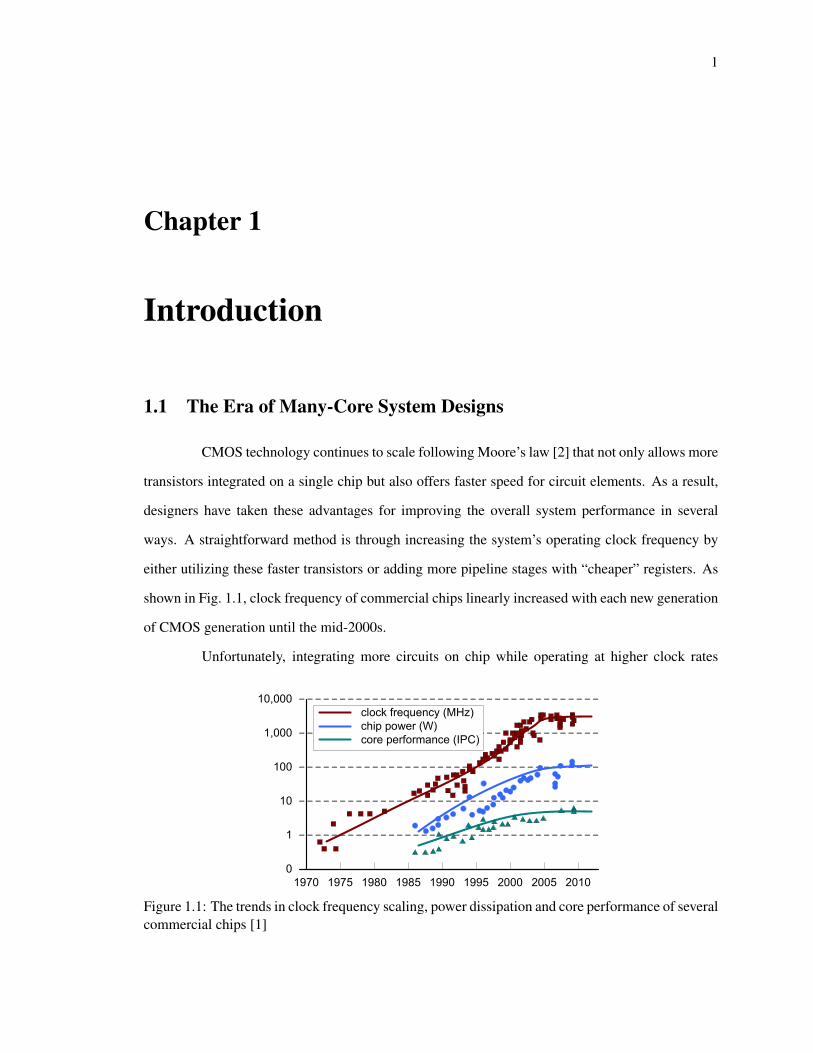
CMOS technology continues to scale following Moore’s law [2] that not only allows more
transistors integrated on a single chip but also offers faster speed for circuit elements. As a result,
designers have taken these advantages for improving the overall system performance in several
ways. A straightforward method is through increasing the system’s operating clock frequency by
either utilizing these faster transistors or adding more pipeline stages with “cheaper” registers. As
shown in Fig. 1.1, clock frequency of commercial chips linearly increased with each new generation
of CMOS generation until the mid-2000s.
Unfortunately, integrating more circuits on chip while operating at higher clock rates
1970 1975 1980 1985 1990 1995 2000 2005 2010
0
1
10
100
1,000
10,000
clock frequency (MHz)
chip power (W)
core performance (IPC)
Figure 1.1: The trends in clock frequency scaling, power dissipation and core performance of several
commercial chips [1]

2
1970 1975 1980 1985 1990 1995 2000 2005 2010
0
1
10
100
1,000
10,000
100,000
1,000,000
10,000,000
# of transistors per chip (x 1K)
# of cores per chip
Figure 1.2: The number of transistors integrated and the number of processing cores built in several
commercial chips [1, 8]
makes the chip dissipate more power. This is because power consumption is tightly proportional
to the overall chip capacitance and the operating clock frequency [3]. Around 2005, chip power
dissipation started hitting a ceiling. Heat sink and fan-cooled systems were no longer easy to cool
the chip as its total power consumption started exceeding 100W [4]. Consequently, clock frequency
no longer increases in order to keep the chip’s dissipated power in the acceptable range.
Improving the system performance can be achieved by adding more features to the proces-
sors making them execute more instructions per clock cycle such as adding more cache, supporting
superscalar, vector computing, very large instruction width, branch speculation, and out-of-order
execution [5]. However, because of the limitation of instruction level parallelism which can be ex-
ploited in present applications, the performance gain has been being diminished as show in Fig. 1.1.
Moreover, processor complexity significantly increases which outweighs the performance gain and
also dissipates a lot more power. As a result, only few new features have been added into the proces-
sors recently; even worse, some expensive features such as speculation and out-of-order execution
have been removed from recent chips to keep their power consumption low [6, 7].
While the core complexity has stopped increasing, the number of transistors which can be
integrated in a single chip keeps going up. Eventually, this drives the system architects to put more
cores on the chip for achieving higher performance by exploiting the thread/task level parallelism of

3
applications instead of the limited instruction level parallelism [5, 9]. Fig. 1.2 confirms this obser-
vation. Since the mid-2000s, when the clock frequency got its limitation along with the core perfor-
mance reaches saturation, the number of cores integrated on a single chip started increasing. This
increase has been taking place even faster than the scaling factor predicted by Moore’s law (about 2
times every 18 months or 2 years) because designers have been preferring to use the optimized and
simple cores rather than the power-hungry complex ones [10,11]. Moreover, once designers become
familiar to many-core design methods, more cores will be likely integrated into the chip even at the
same CMOS process. Following the trend shown in this figure, we could see 200+ cores on a chip
in 2015; and 1000-core chips would be possible in 2020. For fine-grain many-core platforms like
AsAP [12, 13], 4000+ cores could be integrated on a single chip in 2020.
1.2 The Scope and Organization of this Dissertation
With a large number of processing cores expected to be integrated on a single chip in
the near future, several challenging issues need to be addressed such as processor designs, inter-
processor interconnections, memory architectures, programming models and languages, application
mapping and scheduling techniques, power management methods, testing and verification flows
and reliability issues [14]. This dissertation mainly focuses on investigating the design, simula-
tion and evaluation of on-chip interconnection networks; other topics are beyond the scope of this
work and are reserved for our future work. The dissertation presents the research results on three
domains of on-chip interconnection networks: high-performance network designs for applications
with high communication bandwidths; low-cost networks for application-specific low-bandwidth
dynamic traffic; and reconfigurable networks for platforms containing many cores operating in inde-
pendent clock domains which target DSP applications with deterministic inter-task communication
characteristics.
The dissertation is organized as follows: Chapter 2 reviews background and related work
on the designs of on-chip networks, and describes the main contributions of this work. Chap-
ter 3 presents a novel on-chip router utilizing shared-queues for achieving high throughput and
low latency on-chip networks. Chapter 4 proposes bufferless on-chip routers for low-cost net-
work designs but still achieve higher performance per unit cost than traditional buffered routers.

4
Chapter 5 presents the design of a reconfigurable source-synchronous on-chip network for globally
asynchronous locally synchronous (GALS) many-core platforms with a real chip design example.
Application mapping on this platform with a case study implementation of a 802.11a baseband re-
ceiver is described in Chapter 6. Chapter 7 concludes this dissertation and suggests main directions
for future work. Many results reported in this work are provided by a network-on-chip simulator
which is presented in Appendix A. Appendix B lists my publications related to the contents of this
dissertation. The glossaries of technical terms used in this dissertation are defined in Appendix C.

5
Chapter 2
Background, Related Work and
Contributions
2.1 On-Chip Network Background
2.1.1 Network Topologies
Point-to-point connections are normally used in systems on chip with a few processing
elements (PEs) because these connections provide the ideal communication performance among
PEs [15]. As shown in Fig. 2.1(a), a 3-PE chip using point-to-point interconnects is simple and
straightforward. However, when the number of PEs increases, the number of direct interconnect
PE
PE PE
PE
PE
PE
PEPE PE
PE
PEPE
PE
(a) (b)
Figure 2.1: Point-to-point interconnects among processing elements (PEs): a) 3 PEs; b) 10 PEs

6
PE PE PEPE
. . .
Figure 2.2: Bus interconnection topology
PE
PE
PE PE
. . .
PE PE
. . .
Ring Switch
Figure 2.3: Ring interconnection topology
links becomes too high as shown in Fig. 2.1(b) that makes them impossible to route due to the
wiring congestion with limited metal layers on chip. Furthermore, each PE must handle a large
number of I/Os making its interface design highly complicated. Therefore, point-to-point intercon-
nect topology is impractical for use in many-core systems.
Another common topology for connecting multiple PEs in a chip is the shared bus struc-
ture as shown in Fig. 2.2 which is used in the Cavium processor [16]. Shared bus architecture
has low area cost and is design-mature which is supported by industrial standards such as ARM
AMBA [17], OpenCores Wishbone [18] and IBM CoreConnect [19]. In addition, supporting broad-
cast communication is its excellent natural characteristic which is useful in shared-memory mul-
ticore systems with a snooping cache-coherence protocol [20, 21]. For a large number of PEs,
however, the design of the central arbiter for handling and granting bus access to PEs becomes
highly complicated. Moreover, the high latency of long global bus length at submicron CMOS
process plus round-trip request-grant signals from PEs to the central arbiter seriously degrades the
overall performance of the system. As a result, this poor scalability prevents the use of the shared
bus interconnect architecture in many-core systems [15].
The ring connection structure as used in Cell processor [22] is a good alternative for the
shared bus. Ring is simple and can be scaled to connect to many cores as shown in Fig. 2.3. Besides
that, the traffic behavior on rings is predictable which is important in debugging and optimizing

7
PE
PE
PE
PE
PE
PE
PE
PE
PE
PE
PE
PE
Switch or Router
Figure 2.4: Mesh interconnection topology
systems. However, when integrating a large number of nodes on the ring, the communication latency
becomes high enough to degrade the overall performance of mapped applications. A result reported
by Kumar et al. showed that the number of elements connected to a bus or a ring should not exceed
20 [23].
For high-performance platforms such as Niagara 2 [24] or application-specific multicore
systems that require real-time interconnection bandwidth, a centralized crossbar fabric is used to
setup fast non-blocking interconnects between processing elements (PE). However, the complexity
and costs of the centralized crossbar are proportional to the square of the number of its ports [25];
thus area and power consumption dramatically increase if increasing the number of PEs.
An adoption in many-core designs is by using many small crossbars in a distributed man-
ner with each crossbar can be viewed as a switch or router that connects to a PE. These switch-
es/routers are interconnected together in some ways to create a larger network. Many distributed net-
work topologies are found in the literature such as fat-tree [26], mesh [27], torus [28], hexagon [29],
spidergon [30], butterfly [31] and dragonfly [32]. Among them, the mesh architecture as shown in
Fig. 2.4 is most popular due to its regular structure with uniform router design, easy scalability and
high compatibility to standard silicon fabrication technologies [33]. Indeed, the mesh network is
used in most of the recent many-core chips such as Intel SCC 48-core [34], TFlops 80-core [35],
Tilera 64-core [36]. In this dissertation, unless otherwise specified, we mainly focus on design and
optimization of routers and switches for 2-D mesh networks (although they could be modified to
work in other topologies).

8
2.1.2 Data Transferring Techniques
There are two common techniques for transferring data among PEs on on-chip networks:
circuit-switching and packet-switching [37]. In circuit-switching network, each source processor
sends a probe message for setting up a path to its destination. When the destination receives the
probe message, it sends an acknowledge message back to the source. Once the source processor
receives this acknowledge message, it sends the whole data message to the destination on the path
which has been setup. After finishing sending the whole data message, the path must be released.
Previous circuit-switching network designs include two separate networks: one for path
settings and one for data transferring [37–39]. The path-setting network acts like a packet-switching
network with buffered routers which speeds up the path setup time by allowing interleaving multiple
probe messages in input router buffers. In Chapter 4 of this dissertation, we propose low-cost circuit-
switching networks using only bufferless routers. The bufferless router is shared for both setup and
data packets instead of two separate networks as in previous work.
In packet-switching network, processors inject data packets into the network as soon as the
network can accept them. They do not need to wait for path setting before sending packets. There
are three basic techniques for forwarding data in packet-switching networks: store-and-forward,
cut-through and wormhole [27]:
• Store-and-forward: router must store the entire packet into its buffer before making a routing
decision.
• Cut-through: router determines the output port and forwards the packet as soon as the packet
header, which contains the destination address, is available. Even though a cut-through router
can achieve lower latency and higher throughput than a store-and-forward router, they both
require large buffers that must be deep enough to store an entire packet in case network
congestion occurs.
• Wormhole: is a specific design of the cut-through router but does not require buffering the
whole packet. It allows flits1 of one packet to spread into many consecutive routers like a
worm, hence its name.
1flit is a flow control unit in a wormhole packet-switched router. A data packet consists of multiple flits: a head flit,
several body flits and one tail flit. Typically, the flit size is equal to the router link width.

9
Due to its buffer-using efficiency, wormhole forwarding technique currently is most pop-
ular in designing on-chip packet-switched routers and is also utilized in all router designs presented
in this dissertation.
2.1.3 Flow-Control Methods
Because the capacity of input buffers is limited, some flow control methods were proposed
to avoid buffer overflow causing packet loss. Three well-know methods among them are credit-
based, handshaking and stop-go [25]:
• Credit-based flow-control: each input buffer calculates how many free entry slots it has, then
sends this information (credit) back to the upstream router. Based on the received credit
information, the upstream router decides how many flits will be sent before stalling or until
the credit is updated. The credit information can be also used for choosing output channels
by adaptive routing algorithms.
• Handshaking flow-control: upstream and downstream routers exchange messages such as ac-
knowledgement (ACK) and non-acknowledgement (NACK) for noticing whether the packets
have been correctly received. The upstream router optimistically sends flits whenever they
become available. If the downstream router has a buffer slot available, it accepts the flit and
sends an ACK back to the upstream router. If no buffer slots are available when the flit arrives,
the downstream router drops the flit and sends a NACK. The upstream router holds onto each
flit until it receives an ACK; if it receives a NACK, it retransmits the flit.
This method is costly because each sending router must store all sent flits until it receives the
corresponding ACK or NACK messages. Besides that, dropping and retransmitting packets
consume extra power. Therefore, this method may be used in computer networks [40] but
is not appropriate for on-chip router designs which have only limited power and silicon area
budgets.
• Stop-and-go (or on/off ) flow-control: only one bit is used to indicate whether the downstream
buffer is full or not. The upstream router keeps sending flits until it notices a full signal from
the downstream router.

10
S
D
S
D
(a) (b)
Intermediate Router
S Source Router
D Destination Router
Figure 2.5: Examples of routing a packet from a source router to a destination router: a) a single
path with XY dimension-ordered routing; b) multiple paths with an adaptive routing. Different
adaptive routing algorithms would provide different numbers of possible paths.
In this dissertation, the on/off flow control is utilized in all bufferless on-chip routers
presented in Chapter 4 while the credit-based method is used for buffered routers proposed in Chap-
ter 3. Because 1-bit synchronizer is safer than multi-bit synchronizers between different clock do-
mains [41, 42], on/off flow control is also used in our reconfigurable source-synchronous networks
for GALS many-core platforms described in Chapter 5.
2.1.4 Routing Strategies
There are two packet routing strategies in on-chip networks: deterministic and adap-
tive [43].2 For 2-D mesh networks, the simplest deterministic routing algorithm is dimension-
ordered. In the XY dimension-ordered routing as depicted in Fig. 2.5(a), each packet is routed on
the X dimension of the array until it reaches the router having the same column as its destination,
then is routed on the Y dimension to reach the destination. YX dimension-ordered routing is in the
similar way but packets are routed on the Y dimension first then on the X dimension to reach the
destinations.
Adaptive algorithms allow routing a packet on multiple paths to its destination as depicted
in Fig. 2.5(b). The output channel of each packet at a router in the network is decided depending on
the congestion condition at the deciding time. This allows packets to avoid congestion channels at
run-time hence can achieve higher network throughput than dimension-ordered routing policies in
several regular traffic patterns. However, without routing constraints, an adaptive routing strategy
may cause network deadlock, livelock, or both.
2Lookup-table based routing is understood as deterministic or adaptive routing depending on how the router chooses
the output channel for a packet at run-time.

11
(a) (b) (c)
Figure 2.6: Examples of network deadlock and deadlock-free routing: a) deadlock caused by a
channel dependent loop from four packet routing paths made by routers in the network; b) deadlock-
free with XY routing: allows only 4 turn types; c) deadlock-free with West-First adaptive routing:
allows up to 6 turn types. In (b) and (c), a turn marked with ‘X’ in red means it is prohibited while
the router routes a packet.
2.1.5 Network Deadlock
A network incurs deadlock when packets in the network indefinitely stop moving. The
main reason for network deadlock is the forming of channel dependent loops from packets in the
network caused by an adaptive routing algorithm [44, 45]. Fig. 2.6(a) shows an example of the
classic deadlock caused by four routers routing packets to their output channels creating a depen-
dent loop. In this situation, each packet waits for its front packet to get moved; however, because
the paths of packets formed a loop, they have indefinitely blocked together causing deadlock. To
avoiding deadlock, some constraints must be applied into routing algorithms for preventing forming
channel dependent loops among packets.
The most simple and well-known deadlock-free adaptive routing strategy is based on the
turn models proposed by Glass [46]. In these models, some turns are prohibited while routing a
packet. For example, the West-First turn model allows six turns as shown in Fig. 2.6(c). In this turn
model, two turns are prohibited, packets are not allowed to turn from the North or South direction
to the West direction. With six allowed turns, it guarantees no channel dependent loop to be formed
from the packet-routing paths. The XY routing policy is a special case of the turn models in that it
only allows four routing turns as depicted in Fig. 2.6(b). Clearly, the West-First model allows more
routing paths than the XY model due to its more allowed turns. In the same class with the West-First
model, there are two other turn models called North-Last and Negative-First [46].
Another turn-based deadlock-free adaptive routing is by eliminating two turns depending
on the current router position of the packet in the network named Odd-Even turn model [47]. For
example, when a packet is traversing a node in an even column, turns from East to North and

12
from North to West are prohibited. For packets traversing an odd column node, turns from East to
South and from South to West are prohibited. Although this Odd-Even model is deadlock-free, it
causes different implementations for routers on even and odd columns. Other deadlock-free adaptive
routing strategies were proposed such as ROMM [48], GOAL [49], O1TURN [50], DyAD [51],
DyXY [52]. However, while they offer only modest performance improvements compared to the
turn models, they are highly complicated which are costly in both design and test thus are rarely
used in practical many-core systems.
Another reason for causing deadlock is because of resource sharing inside a router design
such as all input ports share the same set of buffer queues [53]. For this architecture, deadlock
can be avoided if the router supports a mechanism allowing packets to avoid indefinitely waiting
on a busy shared resource. A solution, which is presented in Chapter 3, is by allowing packets to
opportunistically bypass busy shared buffer queues.
An uncommon but hard-detected deadlock reason is because of the programmers while
mapping applications on a many-core system. Even though the underlying on-chip network is
deadlock-free, the software protocol created by a programmer may cause deadlock [54]. The
protocol-based deadlock problem is out of the scope of this work, in which we assume the program-
mers themselves are aware of the deadlock potential while implementing applications on many-core
platforms.
2.1.6 Network Livelock
Another concern while designing a routing algorithm is network livelock. Livelock hap-
pens when a packet moves indefinitely in the network without ever reaching its destination even
though there is no deadlock. The main reason causing network livelock is by a non-minimal adap-
tive routing. Non-minimal routing allows packets to misroute out of the shortest paths to the des-
tinations. Without a certain mechanism, a misrouted packet can be misrouted again in next routers
hence moves indefinitely around in the network without reaching its destination. The simplest so-
lution to avoid livelock is to use the XY dimension-ordered or minimal adaptive routing strategies
such as turn models mentioned above. Another solution is to limit the number of misrouted times
of a packet. When its misrouted times hit a threshold, it is forced to go on the minimal paths to its

13
destination.
Livelock may also occur in the network of bufferless routers using a packet deflecting
or dropping strategy. Packet deflecting causes packet misrouted hence could lead to livelock. A
dropped packet will be retransmitted by its source; however it may be dropped again thus can never
reach its destination. The solution for avoiding these kinds of livelock is by timestamping the
transmitted packets [55]. Packet’s timestamp is initialized at zero and increases with each network
clock cycle. When network congestion happens, a packet with the highest timestamp is prioritized
to go on the minimal path and is not dropped hence is guaranteed to reach its destination. Because
timestamping of a packet increases with each clock cycle, a packet (even misrouted or dropped)
eventually will have its timestamp to be greatest compared to others hence get prioritized to route
to its destination. Therefore, there is no livelock for every packet.
Livelock also occurs at routers with an unfair resource allocation policy. With bad luck, a
packet may never win the resource arbitration, hence does not have the chance to move even if there
is no deadlock (other packets still get granted to advance in the network). A simple solution to avoid
this livelock case is using fair resource arbitration such as round-robin or oldest-first arbiters [25,43].
In this dissertation, we utilize both XY-routing and minimal turn-based routing algorithms
along with round-robin arbiters for all the proposed routers for avoiding network deadlock and
livelock.
2.2 On-Chip Router Designs
2.2.1 Basic Circuit Components of a Router
Fig. 2.7 depicts a multicore system in which processors communicate together through a
2-D mesh network of routers. Each router has five ports which connect to four neighboring routers
and its local processor. A network interface (NI) locates between a processor and its router for
transforming processor messages into packets to be transferred on the network and vice versa.
A typical router architecture is shown in Fig. 2.8. The figure only shows details of one in-
put port for simple view. At first, when a flit arrives at an input port, it is written to the corresponding
buffer queue. Assuming without other packets in the front of the queue, the packet starts deciding
the output port using its routing computation circuit implementing either the XY dimension-ordered

14
Core
RNI
buffer
buffer
buffer
bu
ffer
bu
ffer
South
North
East
Wes
t
Local
Xbar
Control
Logic
Figure 2.7: Multiple processing cores in a chip are interconnected by a 2-D mesh network of routers.
NI: Network Interface; R: Router.
buffer
Routing
Comp.
Switch
Arbiters.
. .
. . .
credits in
. . .
credit out
flit in flit out
. . .
. . .
P x P
Crossbar
in port
state
out port
states
. . .
Figure 2.8: A typical buffered router architecture. P: the number of router ports.
or an adaptive routing algorithm. After that, it arbitrates for its output port because there may be
multiple packets from different input queues having the same desired output port. If it wins the out-
put switch allocation, it will traverse across the crossbar and the output link toward the downstream
router.
Therefore, a router typically has five basic circuit components: buffers for temporarily
holding packets, routing circuits for determining the output channels of packets, arbiters to handle
access permission to output channels by multiple packets, a crossbar for switching packets from
input buffers to output channels. In addition, the router also includes credit counters for maintaining
the available slots of buffers used by a flow controlling policy. It also contains simple finite state
machines for keeping track the states of input and output ports (idle, wait, busy) which are used by

15
internal router operations as described above.
2.2.2 High-Performance Router Designs
If the input buffer has only one queue and the router uses wormhole packet transferring
technique, the router is called a wormhole (WH) router. In a WH router, if a packet at the head of
a queue is blocked (because it is not granted by the switch arbitration (SA) or the corresponding
input queue of the down stream router is full), all packets behind it also stall. This head of line
blocking problem can be solved by a virtual-channel (VC) router [56]. In this VC router design,
an input buffer has multiple queues in parallel, each queue is called a virtual-channel, that allows
packets from different queues can bypass each other to advance to the crossbar stage instead of
being blocked by a packet at the head queue. Because now an input port has multiple VCs, a virtual-
channel allocator (VCA) is needed to allocate available output VCs for each input VC before packets
in input VCs get granted by the SA to traverse to the next routers. Although VC router improves
the network throughput, the VCA operation added in each router increases the packet latency.
Peh et al. and Mullins et al. proposed speculative techniques for VC routers allowing a
packet to simultaneously arbitrate for both VCA and SA giving a higher priority for non-speculative
packets to win SA; therefore reducing low-load latency in which the probability of failed speculation
is small [57, 58]. This low latency, however, comes with the high complexity of SA circuitry and
also wastes more power each time the speculation fails. A packet must stall even if it wins SA but
fails VCA, and then has to redo both arbitration at the next cycle. When the network load becomes
heavy, speculation often fails hence speculative routers achieve the same throughput as VC routers
while consuming higher power and energy.
An express virtual channel (EVC) router architecture was proposed by Kumar et al. which
uses virtual lanes in the network to allow packets to bypass nodes along their paths in a non-
speculative fashion, hence reduces packet delay and improve network throughput [59]. However,
an EVC router requires a complicated fine-grained buffer management which allows sharing buffer
slots among normal and express VCs. The total number of VCs (both normal and express) is large
that complicates the VC allocator designs and is costly in terms of area and power. A complex flow
control is needed to avoid starvation because packets on express VCs have higher priorities than
16
normal VCs. Moreover, EVC router only works with a dimension-ordered routing policy, does not
work with adaptive ones.
Another approach for boosting the network throughput over certain regular traffic patterns
and application-specific traces by maximizing channel utilization with bidirectional links was pro-
posed by Lan et al. [60]. In their proposed BiNoC network, when an output channel of a router
is idle, it can be used as an input channel. Therefore a router can send two flits in parallel in two
bidirectional links to the next router. This method allows achieving better network performance
when the traffic is heavy in one direction of nearest neighboring router pairs. However, the router
buffer space is doubled because it needs buffers for both input and output channels. Besides that,
the control circuits for avoiding data conflict on bidirectional links are also complicated. As a re-
sult, BiNoC router has much higher area and power costs and consumes higher energy than typical
routers.
Chapter 3 in this dissertation presents another approach for achieving high network through-
put with low average energy per packet by allowing multiple input packets to share a set of buffer
queues. Sharing buffers maximizes the buffer utilization for reducing packet stall times thus im-
proving the overall network throughput. The router also allows packets to bypass shared-queues
hence reduces packet latency at low loads without the need of speculation.
2.2.3 Low-Cost Router Designs
Along with high-performance on-chip networks, the research domain on low-cost router
designs is becoming increasingly attractive due to the tightly constrained area and power budgets
for each circuit module in many-core chips. Kim proposed a low-cost router design in which the
crossbar is partitioned to support different traffic on X and Y directions [61]. All operations of the
router are combined into one cycle with the input buffers are reduced to only two slots which are
fit enough to cover the round-trip flow-control delay. However, intermediate buffers are added for
packets turning from the X direction to the Y direction which adds more cost to the router. The
arbitration policy which prioritizes packets in flight may cause unfairness hence needs a sophisti-
cated mechanism for avoiding starvation. Moreover, this router does not support adaptive routing
strategies.

17
Low-swing crossbar and link designs reduce router power by operating at lower supply
voltages [62, 63]. However, these designs use custom circuit modules which have high design and
test costs than standard-cell based designs. While other router components are supplied by regular
voltages, low supply voltages for crossbar and links need additional voltage-level converters which
also increase the router complexity. Some previous work also proposed using voltage and frequency
scaling (VFS) technique for saving dynamic router power [64–66]. These designs requires sophisti-
cated control circuits with significant area overhead. Besides that, router traffic frequently changes
cycle by cycle making these VFS control circuits often active hence consume extra power which
diminishes the power saving achieved by the VFS itself.
It has been observed that buffers consume the largest portions of the whole router area and
power [67]; therefore, bufferless designs which totally remove buffers out of the routers, recently,
are becoming more attractive. Michelogiannakis et al. proposed elastic routers which use elastic
pipelining latches on inter-router links as storage elements instead of explicit input buffers [68].
With this approach, the channels act as small FIFOs hence allow elastic routers to operate similarly
to buffered wormhole routers. Elastic elements are built from latches and using the “ready-valid”
handshake flow controlling method. Latches, however, are not well compatible with CAD tools
which have timing analysis and optimization algorithms based on edge-triggered registers. More-
over, handshaking flow control requires non-trivial sophisticated circuit designs.
Another approach for bufferless router designs is to utilize a “hot-potato” routing principle
which either drops the flit or deflects it to another output port if its desired output port is busy [55,69–
71]. Dropping flits requires the router to support a mechanism for noticing the sources to retransmit
the dropped packets. Deflecting flits causes flits to go to non-minimal paths which are potential
for deadlock and livelock. Therefore, the routers must add more complex control logic and priority
scheduling circuits to avoid these problems. As a result, these previous bufferless router designs
were shown to consume even higher energy than buffered routers [72]. Furthermore, flit dropping
and deflecting cause the out-of-order delivery of not only packets but also the flits of each packet.
This requires additional buffers at receiving processors for reordering flits and packets before they
are consumed by the processors. The area and power consumed by these reordering buffers can be
higher than the buffers removed from the routers hence negates the initial benefit of the ideas in
designing bufferless routers.

18
The proposed bufferless router designs presented in Chapter 4 guarantee in-order packet
delivery without packet dropping or deflecting hence achieves lower area and power with higher
performance per unit cost than buffered routers. Clock-gating is another well-known and efficient
method for reducing dynamic power which has been well applied for on-chip routers [73]. We also
apply clock-gating for all router designs presented in this dissertation.
2.3 Communication Methods for GALS Many-Core Systems
For practical digital designs, clock distribution becomes a critical part of the design pro-
cess for any high performance chip [74]. Designing a global clock tree for a large many-core chip
becomes very complicated and it can consume a significant portion of the power budget, which can
be up to 40% of the whole chip’s power [4]. One effective method to address this issue is through
the use of globally-asynchronous locally-synchronous (GALS) architectures where the chip is parti-
tioned into multiple independent frequency domains. Each domain is clocked synchronously while
inter-domain communication is achieved through specific interconnect techniques and circuits [75].
Due to its flexible portability and “transparent” features regardless of the differences among compu-
tational cores, GALS interconnect architecture becomes a top candidate for multi- and many-core
chips that wish to do away with complex global clock distribution networks.
The methodology of inter-domain communication is a crucial design point for GALS
architectures. One approach is purely asynchronous clockless handshaking, which uses multiple
phases (normally two or four phases) of exchanging control signals (request and ack) for transfer-
ring data words across clock domains [76,77]. Unfortunately, these asynchronous handshaking tech-
niques are highly complicated and use unconventional circuits (such as the Muller C-element [3])
typically unavailable in generic standard cell libraries. Besides that, because the arrival times of
events are arbitrary without reference timing signals, their activities are difficult to verify in tradi-
tional digital CAD design flows.
The so-called delay-insensitive interconnection method extends the clockless handshak-
ing techniques by using some coding techniques such as dual-rail or 1-of-4 for avoiding the re-
quirement of delay matching between data bits and control signals [78]. These circuits also require
specific cells that do not exist in common ASIC design libraries. Quinton et al. implemented a

19
delay-insensitive asynchronous interconnection network using only digital standard cells; however,
the final circuit has area and energy requirement many times larger than those of a synchronous
design [79].
Another asynchronous interconnect technique is by using pausible or stretchable clock
where the rising edges of the receiving clock is paused following the requirements of the control
signals from the sender. This makes the synchronizer at the receiver wait until the data signals
stabilize before sampling [80,81]. The receiving clock is artificial meaning its period can vary cycle
by cycle; so it is not particularly suitable for a processing elements with synchronous clocking that
need a stable signal clock in a long enough time.
An important note is that all asynchronous techniques mentioned above were conven-
tionally proposed for point-to-point interconnects [82–84]. When applied to router designs with
multiple input ports, these techniques become very difficult to manage due to the arbitrary and un-
predictable arrival times of multiple input signals. They require adding more sophisticated circuits
mainly for ensuring the router to operate correctly; and needless to say, the router becomes very
complicated to test and debug [85].
An alternative for transferring data across clock domains is the source-synchronous com-
munication technique that was originally proposed for off-chip interconnects. In this approach, the
source clock signal is sent along with the data to the destination. At the destination, the source clock
is used to sample and write the input data into a FIFO queue while the destination clock is used to
read the data from the queue for processing. This method achieves high efficiency by obtaining
an ideal throughput of one data word per source clock cycle with a very simple design that is also
similar to the synchronous design method; hence it is friendly with common digital standard cell
design flows [13, 86, 87].
In addition, a source-synchronous communication path can also be scaled, allowing easy
setup of a long-distance interconnection between two arbitrary processors. Using dual-clock FIFOs
for interfacing between clock domains is also easy to be applied to multi-port router designs rather
than only short-distance point-to-point interconnects as by asynchronous handshaking techniques.
Due to its advantages, we adopt the source-synchronous communication technique for designing a
ultra low cost and high-performance reconfigurable on-chip networks for many-core GALS plat-
forms which is presented in Chapter 5.

20
2.4 Contributions
The main contributions presented in this dissertation are:
• It presents an on-chip network router design using shared-queues [88, 89]. Sharing buffer
queues in the router allows maximizing its buffer utilization hence achieves high network
throughput by reducing packet stall times at input ports. The router also achieves low latency
by allowing packets to effectively bypass shared-queues when the network loads become
low. Due to its higher performance, which allows it to transfer more packets in a certain
time window, the shared-queue router also consumes lower energy per transferred packet
compared to virtual-channel routers. Experimental results show that, averaged over a broad
range of traffic patterns, the proposed shared-queue router has 18% higher throughput, 17%
lower latency and 9% lower energy per packet than virtual-channel routers given the same
buffer space capacity.
This work received a Best Paper Award at the IEEE International Conference on Computer
Design (ICCD) in 2011.
• It investigates approaches for designing low-cost on-chip networks with bufferless routers [90,
91]. Bufferless routers achieve ultra low area and power costs by removing costly physical
buffers out of the router datapath. The proposed bufferless routers also guarantee deliver-
ing data packets in-order, hence eliminate the need of highly complex reordering buffers at
processors. The bufferless router designs cover both packet-switching and circuit-switching
techniques. Experimental results show that, the proposed bufferless packet-switched router is
33% less area, 10% lower power 25% higher throughput, 30% lower latency and 27% lower
energy per bit than the smallest buffered router. The proposed bufferless circuit-switched
router is 32% less area, 10% lower power, 42% higher throughput, 28% lower latency and
34% lower energy per bit than the smallest buffered router.
• It presents a GALS-compatible source-synchronous reconfigurable on-chip network for many-
core platforms [92, 93]. The platforms mainly target streaming digital signal processing and
embedded applications which typically have a high degree of task-level parallelism among
computational kernels and deterministic inter-task communication traffic patterns. A GALS

21
167-processor chip named AsAP2 equipped with this network was implemented in 65 nm
CMOS showing the network area to be only 7% of the processor core and to dissipate about
10% of total power while running a complex application [13].
• It describes an example mapping implementation of a complete IEEE 802.11a/11g baseband
receiver on AsAP2 [94,95]. The implementation occupies 25 processors which is 30% fewer
processors compared to a version mapped on a platform having only nearest neighbor inter-
connects. The receiver achieves a real-time throughput of 54 Mbps and consumes 130 mW
which is 1.7 times faster and 2.1 times lower power compared to an implementation on the
state-of-the-art software defined radio SODA processor [96].
• It reports an open-source simulator for early exploration of performance and energy efficiency
of networks on-chip [97]. This simulator has been developed using SystemC, a C++ plugin,
which allows fast modeling of concurrent hardware modules at the cycle-level accuracy. The
statistic output results provided by the simulator are the average network latency, throughput,
router power and energy per transferred data bit. Area, timing and power of router compo-
nents are post-layout data based on a 65 nm CMOS standard-cell library.

22
Chapter 3
High-Performance On-Chip Networks
with Shared-Queue Routers
In a typical router, each input port has an input buffer for temporarily storing packets in
case that output channel is busy. This buffer can be a single queue as in a wormhole (WH) router or
multiple queues in parallel as in virtual-channel (VC) routers [56]. These buffers, in fact, consume
significant portions of area and power that can be more than 60% of the whole router [87]. Bufferless
routers remove buffers from the router so save much area [55, 70]; however, their performance
becomes poor in case packet injection rates are high. Due to having no buffers, previous router
designs proposed to drop and retransmit packets or to deflect them once network contention occurs
that can consume even higher energy per packet than a router with buffers [72] (Chapter 5 proposes
other approaches for designing bufferless routers which achieves lower energy per transferred packet
than buffered routers).
Another approach is by sharing buffer queues that allows utilizing idle buffers [98] or
emulating an output buffer router in order to obtain higher throughput [99]. Our work differs from
those router designs by allowing input packets at input ports to bypass shared queues so that it
achieves lower zero-load latency. In addition, the proposed router architecture has simple control
circuitry making it dissipate less packet energy than VC routers while achieving higher throughput
by letting queues share workloads when the network load becomes heavy.
The main contributions of this chapter are:

23
• exploring and analyzing shared-queue router architectures that maximize buffer utilization
for boosting network throughput.
• proposing a router architecture which allows input packets to bypass shared queues for reduc-
ing zero-load packet latency.
• evaluating and comparing the proposed router with VC routers in terms of latency, throughput,
power, area and packet energy over both synthetic and embedded application traffic patterns.
This chapter is organized as follows: Section 3.1 provides the motivation of this work.
Section 3.2 presents our router architecture with all its components in details. The experimental
results are shown in Section 3.3 with analysis and comparison against VC routers. Section 3.4
reviews related work and, finally, Section 3.5 summarizes the chapter.
3.1 Motivation
We first review conventional on-chip router architectures with brief evaluation of their
performance, and then drive the motivation of our new router design using shared queues.
3.1.1 Typical Router Architectures
Fig. 3.1(a) shows a typical WH router with four pipeline stages. The figure shows details
of only one input port for simple view. The traveling process of a flit through a WH router is
described as follows:
• At first, when a flit arrives at an input port, it is written to the corresponding buffer queue.
This step is called buffer write (BW) or queue write (QW).
• Assuming without other packets in the front of the queue, the packet starts deciding the output
port for its next router (based on the destination information contained in its head flit) instead
of for the current router (known as lookahead routing computation (LRC) [100]). At the
same time, it arbitrates for its output port at the current router because there may be multiple
packets from different input queues having the same output port. This step is called switch
allocation (SA).

24
(a) (b)
queue
Routing
Comp.
Switch
Allocator
. . .
. . .
credits in
. . .
credit out
flit in flit out flit in
Routing
Comp.Switch
Allocator
VC
Allocator. . .
credits in
. . .
. . .
credits out
flit out
. . .
. . .
. . .P : P
Xbar
. . .P : P
Xbar
queue
queue
. . .
in port
state
in VC
states
. . .
. . .
out port
states
. . .
LRC
SAST LT
LRC
VCASA ST LT
out VC
states
. . .
Head flit
ST LTBody or Tail flits SA ST LT
Head flit
Body or Tail flits
QW
QW
QW
QW
Figure 3.1: Typical router architectures and their pipelines: (a) 4-stage wormhole (WH) router;
(b) 5-stage virtual-channel (VC) routers. QW: Queue Write; LRC: Lookahead Route Computation;
VCA: Virtual Channel Allocation; SA: Switch Allocation; ST: Switch Traversal; LT: Output Link
Traversal; (X): a pipeline bubble or stall. P: the number of router ports.
• If it wins the output switch allocation, it will traverse across the crossbar. This step is called
crossbar traversal or switch traversal (ST).
• After that, it then traverses on the output link towards next router. This step is called link
traversal (LT).
Both LRC and SA are done by the head flit of each packet; body and tail flits will follow
the same route that has already been reserved by the head flit, except the tail flit should release the
reserved resources once it leaves the queue.
Although there are different ways to pipeline a router, a typical wormhole router is nor-
mally pipelined into four stages as shown in Fig. 3.1(a) corresponding to four operating steps de-
scribed above [25]. This is similar to how we pipeline a traditional processor into five stages cor-
responding to its five basic operating steps: instruction fetch (IF), instruction decode (ID), execute
(EX), memory access (MEM), and register write back (WB).
In a WH router, if a packet at the head of a queue is blocked (because it is not granted
by the SA or the corresponding input queue of the down stream router is full), all packets behind it

25
0 0.1 0.2 0.3 0.4 0.50
20
40
60
80
100
injection rate (flits/cycle/node)
netw
ork
late
ncy (
cycle
s)
WH (16 entries)
VC (2 VCs x 8 entries)
VC−fullXbar (2 VCs x 8 entries)
Figure 3.2: Average packet latency simulated on a 8×8 2D-mesh network over uniform random
traffic pattern
also stall. This head of line blocking problem can be solved by a virtual-channel (VC) router [56] as
shown in Fig. 3.1(b). In this VC router design, an input buffer has multiple queues in parallel, each
queue is called a virtual-channel, that allows packets from different queues to bypass each other to
advance to the crossbar stage instead of being blocked by a packet at the head queue (however, all
queues at one input port can be still blocked if all of them do not win SA or if all corresponding
output VC queues are full).
Because now an input port has multiple VC queues, each packet has to choose a VC of
its next router’s input port before arbitrating for output switch. Granting an output VC for a packet
is given by a virtual-channel allocator (VCA); and this VC allocation is performed in parallel with
the LRC; hence the router now has five stages as shown in Fig. 3.1(b). As a result, although a VC
router achieves higher saturation throughput than a WH router while having the same number of
buffer entries per input port, it also has higher zero-load latency due to deeper pipeline.
Fig. 3.2 shows the latency-throughput curves of a 8×8 2-D mesh network over uniform
random traffic pattern with packet length of 4 flits. As shown in the figure, a VC router with 2
queues per input port (each queue has 8 entries) has 11% throughput gain compared to a WH router
with 16 entries per queue; but its zero-load latency is 36 cycles that is also 20% higher than that of
a WH router (30 cycles).

26
Figure 3.3: Power and area costs of circuit components in a VC router with 2 VCs × 8 flits per input
port: (a) power breakdown; (b) area breakdown.
. . .
. . .P : P
Xbar
queue
queue
. . .
. . .
. . .(PxV) : P
Xbar
queue
queue
. . .. . .
(a) (b)
Figure 3.4: Crossbar designs for a virtual-channel router: (a) P:P crossbar with V buffer queues of
an input port are multiplexed; (b) PV:P crossbar that connects directly to all input buffer queues.
P: the number of router ports; V: the number of queues per input port.
3.1.2 Opportunities for Achieving Higher Throughput
Fig. 3.3 shows area and power breakdowns of a 2×8 VC router synthesized on a 65-nm
CMOS process. As shown, buffer queues occupy 54% area and consume 70% power of the whole
router; while crossbar consumes only 8%. If we use a higher radix crossbar, we could achieve
higher throughput with a cost overhead still small compared to the cost of buffers as will be shown
in Section 3.3.
Fig. 3.4 shows two crossbar designs for VC routers. The first one is for the traditional
VC router where the input queues of each input port are multiplexed before being connected to the
crossbar. The second one allows all input queues to connect directly a full input degree crossbar.
With this full-degree crossbar, after allocated an output VC, a packet from a queue can directly
arbitrate for its output port then would advance to next router if it wins; while with multiplexed-
input crossbar, queues of the same input port have to compete together first before arbitrating for
an output port. Clearly, the probability of winning both arbitration stages is less than winning only
one arbitrator; hence, a VC router with full-crossbar (full-Xbar) achieves higher throughput than a

27
typical VC router given the same number of VCs and buffer entries as also shown in Fig. 3.2.
We also observe that, although the buffers are costly, they are not well utilized. Given an
on-chip communication traffic, not all input queues have packets for processing at the same time.
A few input ports can receive packets all the time while others are often empty. Clearly, we wish
at this situation, idle queues would share their storage capacity with busy queues at other input
ports that would allow more packets to be advanced rather than to be stalled, hence should improve
more throughput. This motivates us to design a router which can maximize the utilization of these
high-cost buffer queues by taking advantage of full-degree crossbars. This router should achieve
the best performance in both cases: when the traffic load becomes heavy, the router allows utilizing
shared buffers reducing packet stall times at input ports so that it can achieve higher throughput than
a full-Xbar VC router; while at low-load packets can bypass shared queues hence has low latency
similar to a wormhole router.
3.2 RoShaQ: Router Architecture with Shared Queues
3.2.1 The Initial Idea
For maximizing queue utilization, input ports of a router can share all queues as depicted
in Fig. 3.5(a). With this architecture, incoming packets from an input port can be written to any
shared queue. However, this architecture has critical drawbacks explained as follows. Because
there is no buffer at input ports, when a packet from a upstream router needs to be forwarded, it
has to send a request to downstream router and wait to receive the grant before sending data. As a
result, the shared queue arbitrator for each router is highly complicated because it must handle many
external requests from multiple shared queues of all neighboring routers. Furthermore, the round-
trip inter-router request/grant delay can take several cycles plus the intra-router pipeline making
zero-load network latency very high [53].
To alleviate this latency, each input port is dedicated one buffer queue and shares all
remaining queues as depicted in Fig. 3.5(b). With this design, since each output port connecting to
an input queue of downstream router, shared queues arbitrate for an output port that is similar to
a wormhole router. Input queues of each router also compete together to get grants to the shared
queues. All request/grant signals are intra-router signals, hence reduces latency and also allocation

28
. . .
queue
queue
queue
. . .
. . .
. . .. . .
queue
queue
. . .
P : (PxV)
shared
queues
Xbar
(PxV) : P
output
Xbar
queue
queue
queue
. . .
. . .
queue
. . .
queue
. . .
. . .. . .
shared queues
(a)
(b)
(c)
shared queues
shared queues
input queues
input queues
P : N
shared
queues
Xbar
N : P
output
Xbar
P : N
shared
queues
Xbar
(P+N) : P
output
Xbar
Figure 3.5: Development of our ideas for sharing buffer queues in a router: (a) shares all queues;
(b) each input port has one queue and shares the remaining queues; (c) allows input packets to
bypass shared queues. P: the number of router ports; V: the number of VC queues per input port in
a VC router; N: the number of shared queues.

29
(P+N) : P
output
Xbar
shared queue
. . .
. . .
P : N
shared
queues
Xbar
. . .
. . .
. . .. . .
Routing
Comp.
in port
state
SQ Rx
state
SQ Tx
state
OPA
out port
states
. . .
SQA
input queue
. . .
. . .
. . .
. . .credits in
credit out
flit in
flit out
. . .
. . .
. . .
credit
1
P
1
N
1
1
P
N
1
P
Figure 3.6: RoShaQ router microarchitecture. SQA: shared-queue allocator; OPA: output port
allocator; SQ Rx state: shared queue receiving/writing state; SQ Tx state: shared queue transmit-
ting/reading state. P: the number of router ports; N: the number of shared queues.
complexity. With this architecture, however, packets from input queues must be buffered into the
shared queues again before being sent to output ports. This is actually unnecessary in the case when
network load is low that unlikely causes much contention at output channels.
From this observation, we move on one more step by allowing input queues to bypass the
shared queues as shown in Fig. 3.5(c). With this design, a packet from an input queue simultane-
ously arbitrates for both shared queues and an output port; if it wins the output port, it would be
forwarded to the downstream router at the next cycle. Otherwise, that means having congestion at
the corresponding output port, it can be buffered to the shared queues. Intuitively, at low load, the
network would have low latency because packets seem to frequently bypass shared queues. While
at heavy load, shared queues are used to temporarily store packets hence reducing their stall times
at input ports that would improve the network throughput. In the next subsection, we will show in
detail circuit components that realize this router architecture.
3.2.2 RoShaQ Architecture
RoShaQ, a Router architecture with Shared Queues based on the idea of Fig. 3.5(c), is
shown in Fig. 3.6. When an input port receives a packet, it calculates its output port for the next
router (lookahead routing), at the same time it arbitrates for both its decided output port and shared
queues. If it receives a grant from the output port allocators, it will advance to its output port in the

30
next cycle. Otherwise, if it receives a grant to a shared queue, it will be written to that shared queue
at the next cycle. In case that it receives both grants, it will prioritize to advance to the output port.
Shared-queues allocator (SQA) receives requests from all input queues and grants the
permission to their packets for accessing non-full shared queues. Packets from input queues are
allowed to write to a share queue only if: 1) the shared queue is empty; or 2) the shared queue is
containing packets having the same output port as the requesting packet. This shared queue writing
policy guarantees deadlock-free for the network as will be explained in Subsection 3.2.5 below.
The output port allocator (OPA) receives requests from both input queues and shared
queues. Both SQA and OPA grant these requests in round-robin manner to guarantee fairness and
also to avoid starvation and livelock. Input queue, output port, shared-queue states maintain the
status (idle, wait or busy) of all queues and output ports, and incorporate with SQA and OPA to
control the overall operation of the router. Only input queues of RoShaQ have routing computation
logic because packets in the shared queues were written from input queues so they already have
their output port information. RoShaQ has the same I/O interface as a typical router that means they
have the same number of I/O channels with flit-level flow control and credit-based backpressure
management [25].
3.2.3 RoShaQ Datapath Pipeline
After a packet has been written into an input queue in the first cycle, in the second cycle
it simultaneously performs three operations: LRC, OPA and SQA. At low network loads, there is
a high chance the packet will the OPA due to low congestion at its desired output port; hence it is
granted to traverse through the output crossbar and output link towards next router. Therefore, it
incurs four stages including link traversal as depicted in Fig. 3.7(a) that is similar to a WH router
pipeline.
When network loads become heavy, the packet at an input queue may fail to get granted
from OPA, but it can get a grant from SQA and is allowed to traverse the shared-queue crossbar and
write to the granted shared queue in next cycles. After that, it arbitrates for the output port again and
would traverse across the output crossbar and output channel toward the next router at next cycles
if it is granted by the OPA at this time. Thus, in this situation, it incurs seven inter-router stages as

31
(a)
Head flit
Body or Tail flits
LRC
OPA
SQA
OST LT
OST LT
(b)
Head flit
Body or Tail flits
LRC
OPA
SQA
at heavy load case:
SQST OPA OST LT
SQST OST LT
QW
QW
at light load case:
QW SQW
QW SQW
Figure 3.7: RoShaQ pipeline characteristics: (a) 4 stages at light load; (b) 7 stages at heavy
load. QW: Queue Write; LRC: Lookahead Routing Computation; OPA: Output Port Allocation;
SQA: Shared Queue Allocation; OST: Output Switch/Crossbar Traversal; LT: Output Link Traver-
sal; SQST: Shared-Queue Switch/Crossbar Traversal; SQW: Shared-Queue Write; (X): a pipeline
bubble or stall.
shown in Fig. 3.7(b). This larger number of traversing stages, in fact, allows the router to utilize
shared-queues for reducing stall times of packets at input queues, hence improves throughput at
heavy network load.
In both cases, body and tail flits of a packet traverse through the router in the same way
as its head flit, except they do not need to arbitrate for resources (output ports and shared queues)
that were already reserved by the head flit. The tail flit should also release these reserved resources
once it leaves the queue.
3.2.4 Design of Allocators
This subsection describes the design of allocators for VC and RoShaQ routers. Let P and
V be the number of router ports and number of VC queues per port in a VC router, respectively. Its
VCA circuit is shown in Fig. 3.8 that has two stages of arbiters [57]. Each arbiter in the first stage
chooses which output VC for a specific input VC; while an arbiter in the second stage chooses an
input VC among several input VCs that were granted to the same output VC at the first stage. In
total, this VCA consists of 2PV (PV:1) arbiters.
Fig. 3.9 shows the SA circuit designs for a typical VC router and for a VC router with full

32
PV : 1
arbiter
(1)
PV : 1
arbiter
(V)
PV : 1
arbiter
(1)
PV : 1
arbiter
(V)
PV : 1
arbiter
(1)
PV : 1
arbiter
(V)
PV : 1
arbiter
(1)
PV : 1
arbiter
(V)
in port (1)
in port (P)
out port (1)
out port (P)
total of 2PV (PV:1)arbiters
. . .
. . .. .
. .
. .. .
. .
. .. .
. .. .
. .. .
. .. .
. .. .
. .
Figure 3.8: Output virtual-channel allocator (VCA) in a virtual-channel router. P: the number of
router ports; V: the number of virtual channels per input port.
crossbar. Because input queues in the typical VC router are multiplexed before being connected to
the crossbar, its SA has two stages as shown in Fig. 3.9(a). The first stage decides which input VC
wins the input crossbar port; while the second stage chooses one among these winning input VCs
for output ports. This SA consists of P (V:1) and P (P:1) arbiters. For a full-Xbar VC router, all
input VCs directly arbitrate for output ports; so its SA consists of P (PV:1) arbiters, each for one
output port as depicted in Fig. 3.9(b).
The OPA and SQA of RoShaQ router are shown in Fig. 3.10. The OPA includes P
V : 1
arbiter
(1)
V : 1
arbiter
(P)
P : 1
arbiter
(1)
P : 1
arbiter
(P)
PV : 1
arbiter
(1)
PV : 1
arbiter
(P)
total of P (V:1) and P (P:1) arbiters total of P (PV:1) arbiters
(a) (b)
. .
. .
. .
. .
. .
. .
. .
. .
. . .
. . .
. . .
Figure 3.9: Output switch allocator (SA) in: a) VC router with crossbar inputs multiplexed; b) VC
router with full crossbar. P: the number of router ports; V: the number of virtual channels per input
port.

33
(P+N) : 1
arbiter
(1)
total of P (P+N:1) arbiters
. .
. .
. . .
(P+N) : 1
arbiter
(P)
. .
. .
N : 1
arbiter
(1)
N : 1
arbiter
(P)
P : 1
arbiter
(1)
P : 1
arbiter
(N)
total of P (N:1) and N (P:1) arbiters
. .
. .
. .
. .
. . .
. . .
Ouput Port Allocator: Shared Queue Allocator:
Figure 3.10: Output port allocator (OPA) and shared queue allocator (SQA) structures in a RoShaQ
router. P: the number of router ports; N: the number of shared queues.
(P+N:1) arbiters; each chooses one queue among input queues and shared queues that have the
same output ports, where N is number of shared queues. In order for the total number of buffer
queues to be identical to that of a VC router (PV queues in total), N is equal to P(V − 1) because
each input port has one queue. So, the OPA is exactly the same as the SA of a full-Xbar VC router.
The SQA includes two stages to allocate P input queues to N shared queues; so its circuit is the
same as the SA of a VC router. This SQA is much low cost than a VCA; as a result, OPA and SQA
of RoShaQ consume less area and lower power than VCA and SA of both typical and full-Xbar VC
routers as will be shown in next section.
3.2.5 RoShaQ’s Properties
• A network of RoShaQ routers is deadlock-free. At light loads, packets normally bypass shared
queues, so RoShaQ acts as a wormhole router hence the network is deadlock-free [44]. At
heavy loads, if a packet cannot win the output port, it is allowed to write only to a shared
queue which is empty or contains packets having the same output port. Clearly, in this case
RoShaQ acts as an output-buffered router which was also shown to be deadlock-free [101].
• A network of RoShaQ routers is livelock-free. Because both OPA and SQA use round-robin
arbiters, each packet always has a chance to advance to the next router closer to its destination;
so the network is also free from livelock.
• RoShaQ supports any adaptive routing algorithm. The output port for each packet is only
computed at its input queue, not at shared queues. Therefore, any adaptive routing algorithm

34
Table 3.1: Router configuration used in experiments. Each router has 80 buffer entries in total
Router Name Description
VC2 2 queues/input port, 8 entries/queue
VC2-fullXbar the same as VC2, but using fullXbar
RoShaQ5 1 queue/input port, 5 shared queues, 8 entries/queue
VC4 4 queues/input port, 4 entries/queue
VC4-fullXbar the same as VC4, but using fullXbar
RoShaQ15 1 queue/input port, 15 shared queues, 4 entries/queue
which works for wormhole routers also works for RoShaQ.
• RoShaQ can be used for any network topology. If we hide all design details inside RoShaQ,
we would see RoShaQ only has one buffer queue at each input port similar to a wormhole
router. Therefore, we can change the number of RoShaQ’s I/O ports to make it compatible
with any network topology known in the literature along with an appropriate routing algo-
rithm.
3.3 Experimental Results
3.3.1 Experimental Setup
Table 3.1 describes six router configurations used in our experiments. VC2 and VC4
have 2 and 4 VC queues per input port, respectively. For fair evaluation, each queue of VC2 has
8 flit-entries while each queue of VC4 has 4 flit-entries. VC2-fullXbar and VC4-fullXbar have
the same buffer configurations as VC2 and VC4 except their crossbars are in full-degree (10:5
crossbar for VC2-fullXbar and 20:5 crossbar for VC4-fullXbar). For comparing with VC2 and VC2-
fullXbar where each has total of 10 queues, RoShaQ5 that has 5 shared queues is used. Similarly,
for comparing with VC4 and VC4-fullXbar where each has total of 20 queues, we use RoShaQ15
that has 15 shared queues. All routers have the same 80 flit buffer entries in total.
For evaluating performance of VC, full-Xbar VC and RoShaQ routers, we developed
three cycle-accurate simulators, each for one router model. Experiments are performed over eight
common synthetic traffic patterns, seven real-world multitask applications and three E3S embedded
benchmarks which have large number of tasks.

35
3.3.2 Latency and Throughput
Synthetic Traffic Patterns
We conducted the experiments over eight common synthetic traffic patterns which cover
a wide range of interconnect patterns on 2D mesh networks [25]. For uniform random traffic, each
source processor chooses its destination randomly with uniform distribution in packet-by-packet
basic. For other patterns, destination of each source node is decided based on the location of the
source as follows 1:
• bit-complement: from [x, y] to [x, y]
• transpose: from [x, y] to [y, x]
• bit-shuffle: from [x2x1x0, y2y1y0] to [x1x0y2, y1y0x2]
• tornado: from [x, y] to [(x+3)%8, (y+3)%8]
• bit-rotate: from [x2x1x0, y2y1y0] to [x0x2x1, y0y2y1]
• neighbor: destination is randomly chosen among four nearest neighbors of the source on a
probability of 80%, and is randomly among other processors on a probability of 20%.
• regional: destination is randomly chosen among processors with distances to the source of at
most 3 on a probability of 70%, and is randomly among other processors on a probability of
30%.
Performance of each router is evaluated by running simulations of 100,000 cycles with
20,000 warmup cycles on a 8×8 2-D mesh network where each network node consists of a processor
and a router. Processors inject and consume packets into and out off the network, and each packet
length is four 32-bit flits. As mentioned in Subsection 3.2.5, we can employ any routing algorithm
proposed in the literature [43] for routers; however, for comparing the performance purely achieved
by different architectural designs, we use the same XY dimension-ordered routing algorithm for all
routers in this work. Latency of a packet is measured from the time its head flit is generated by the
1Here x, y are values of horizontal and vertical coordination of a node in a 8×8 mesh; x2 x1 x0 and y2y1y0 are binary
representatives of x and y, respectively.

36
0 0.1 0.2 0.3 0.4 0.50
20
40
60
80
100
injection rate (flits/cycle/node)
netw
ork
late
ncy (
cycle
s)
VC2
VC2−fullXbar
RoShaQ5
VC4
VC4−fullXbar
RoShaQ15
Figure 3.11: Latency-throughput curves over uniform random traffic
source to the time its tail flit is consumed by the destination. Average network latency is the mean
of latency of all packets in the network.
The average packet latency of networks corresponding to six router configurations over
uniform random traffic is given in Fig. 3.11. As shown, even having the same number of buffer
entries, VC4 has higher saturation throughput than VC2 that is identical with results reported by
Peh et al. [57].2 Increasing the number of crossbar input ports improves throughput significantly.
As shown, VC2-fullXbar achieves saturation throughput even higher than VC4. VC4-fullXbar has
15% saturation throughput higher VC4 (0.39 flits/cycle vs. 0.35 flits/cycle).
RoShaQ5 achieves a saturation throughput of 0.37 flits/cycle which is 3% higher than
VC2-fullXbar. RoShaQ15 achieves 0.40 flits/cycle throughput that is 3% higher VC4-fullXbar and
14% higher than VC4. More importantly, both RoShaQ5 and RoShaQ15 have zero-load latency
of 30 cycles similar to a WH router that is 17% lower than all VC routers with and without a full-
degree crossbar (36 cycles). From these results, for simplicity, from now on we only provide the
comparison results among RoShaQ15, VC4 and VC4-fullXbar in the rest of this chapter. Compari-
son among RoShaQ5, VC2 and VC2-fullXbar gives a similar conclusion.
We run simulations for all eight synthetic traffic patterns; zero-load latency and through-
put of routers are listed in Table 3.2. As shown, RoShaQ outperforms both VC routers in seven
traffic patterns, except in transpose pattern. For transpose traffic, routers on the same row send
2Saturation throughput is defined as the injection rate at which network latency reaches about three times of the
zero-load latency [59]. In this work, the saturation throughput is assumed when network latency is 100 cycles.

37
Table 3.2: Zero-load latency and saturation throughput of routers over eight different synthetic
traffic patterns
Zero-Load Latency (cycles) Sat. Throughput (flits/cycle/node)
Traffic Patterns VC4 VC4-fullXbar RoShaQ15 VC4 VC4-fullXbar RoShaQ15
random 36.01 36.01 29.83 0.35 0.39 0.40
bit-complement 49.06 49.06 40.27 0.18 0.20 0.21
transpose 39.71 39.71 32.73 0.17 0.17 0.17
bit-shuffle 30.01 30.01 24.97 0.21 0.22 0.23
tornado 46.85 46.85 38.53 0.22 0.26 0.27
bit-rotate 30.04 30.04 25.01 0.20 0.23 0.24
neighbor 14.30 14.30 12.38 0.75 0.80 0.83
regional 22.68 22.68 19.08 0.60 0.69 0.76
Average 33.58 33.58 27.84 0.33 0.37 0.39
packets to the same output direction; therefore, at saturation, throughput is limited by the output
channel of the last router on that row. So all routers have the same saturation throughput of 0.17
flits/cycle.
Especially, for neighbor and regional patterns, because destination of each packet is quite
close to its source, the network incurs less congestion. Therefore, packets in RoShaQ routers often
bypass shared queues to achieve both lower latency and higher throughput than both VC routers.
On average over all eight traffic patterns, RoShaQ is 18% and 5% higher throughput than VC and
VC-fullXbar routers, respectively with 17% lower zero-load latency.
Real Application Communication Traffic
Many DSP and embedded applications can be represented by a communication task graph
where each task can be mapped onto one or multiple processing units (processors, accelerators or
memory modules) [95]. Fig. 3.12(a) depicts the task graph of a Video Object Plan Decoder (VOPD)
application [102] which also shows the inter-task communication bandwidth requirements.
For generating the experimental traffic of this application, we adopted the method pro-
posed by Hu et al. [103] and Lan et al. [60]. In this method, we transform the required bandwidth
on each inter-task connection into the injection rate of the corresponding sending task. A task which
requires large sending bandwidth also has large injection rate, and vice versa. Let bwi and bw j be
the required bandwidth of tasks Ti and T j to other tasks in the communication graph, then injection

38
T10
T0
T1
T2
T3
T4
T5
T6
T7
T8
T9
T11T14
T12
T13
T15
70
16
362
362
362
49
357353
300
313
313
50094
16
16
16
16
157
16
16
16
27
T10
T0
T1
T2
T3
T4
T5
T6
T7
T8
T9
T11T14
T12
T13
T15
0.070
0.016
0.362
0.362
0.362
0.049
0.3570.353
0.300
0.313
0.313
0.5000.094
0.016
0.016
0.016
0.016
0.157
0.016
0.016
0.016
0.027
(a) (b)
j
i
j
i
bw
bw
fir
fir=
Figure 3.12: Communication graph of a video object plan decoder application (VOPD) and the
corresponding injection rate of each processor used in our simulation: (a) required inter-task band-
widths in Mbps; (b) the corresponding injection rates of processors in flits/cycle.
Table 3.3: Seven embedded applications and three E3S benchmarks used in our experiments
Applications No. Tasks Net. Size
Video object plan decoder (vopd) [102] 16 4×4
Multimedia system (mms) [104] 25 5×5
Multi-window display (mwd) [105] 12 4×3
WiFi baseband receiver (wifirx) [94] 25 5×5
H.264 CAVLC encoder (cavlc) [106] 16 4×4
MPEG4 (mpeg4 [107] 12 4×3
Video conference encoder (vce) [108] 25 5×5
E3S auto-indust (autoindust) [109] 24 6×4
E3S consumer (consumer) [109] 12 4×3
E3S telecom (telecom) [109] 30 6×5
rates of tasks Ti and T j on the corresponding links follow the equationf iri
f ir j
=bwi
bw j
. Therefore, if
given an injection rate of any task, we can easily calculate injection rates for all other tasks on all
links in the graph.
Fig. 3.12(b) shows an example for setting the injection rates of tasks which are corre-
sponding to the communication graph of VOPD application given in figure (a). In this example, if
we choose injection rate for task T0 to task T1 is 0.07 flits/cycle, then injection rate for task T1 to
task T2 is 0.07 × 362 / 70 = 0.362 flits/cycle. Similarly, we can drive injection rates for all tasks in
the application graph as shown in the figure.
In this work, we use communication graphs of seven real-world applications and three
E3S embedded benchmarks [109] which have large numbers of tasks for our experiments. Ap-

39
00.10.20.30.40.50.60.70.80.9
1
vopd
mwd
mm
svc
e
wifirx
cavlc
mpe
g4
auto
indu
st
cons
umer
teleco
m
aver
age
no
rmalized
late
ncy
VC4 VC4-fullXbar RoShaQ15
Figure 3.13: Normalized latency of real applications
plication names and their number of tasks are shown in Table 3.3. Depending on the number of
application tasks, we decide the network size correspondingly. For example, an application with 16
tasks is mapped on a 4×4 network, an application with 24 tasks is mapped on a 6×4 network, and
so on which are also shown in Table 3.3. After network size for each application has been decided,
each task is randomly mapped to one processor in the network.
For evaluation of these embedded applications, we fix the injection rates of all tasks,
then application running latency is measured after a total of one million packets are successfully
transferred. For each application, we assume that the most busy task spends 50% times for execution
and 50% times for communication which means it aggressively executes one cycle and then sends
one output to the downstream task in next cycle, repeatably. With this assumption, the most busy
task in each application has an injection rate of 0.5; the injection rates of other tasks are computed
according to the their required bandwidth given in the graph using the method described above.
For clear comparison, we normalize the latency of each application running on different
routers to the latency when running on the typical VC router which are shown in Fig. 3.13. As
shown, RoShaQ has lower latency than both VC routers in all ten applications. On average, RoShaQ
is 26% and 12% lower latency than VC and VC-fullXbar routers, respectively.

40
Power (mW)
0
10
20
30
40
50
60
70
VC4
VC4-
fullX
bar
RoS
haQ15
Pow
er
(mW
)
Buffers Crossbar
Allocators Others
(a)
00.010.020.030.040.050.060.070.080.090.1
VC4
VC4-
fullX
bar
RoS
haQ15
Are
a (
mm
^2)
(b)
Figure 3.14: Synthesis results: (a) power; (b) area.
Table 3.4: Router power at 1.2V, 1GHz and area comparison
VC4 VC4- vs. RoShaQ15 vs. vs. VC4-
fullXbar VC4 VC4 fullXbar
Power (mW) 56.08 60.05 + 7% 58.26 + 4% -3%
Area (mm2) 0.078 0.093 +19% 0.091 +16% -3%
3.3.3 Power, Area and Energy
Three router models (VC4, VC4-fullXbar and RoShaQ15) in Verilog RTL are synthe-
sized targeting a 65 nm low-power CMOS standard-cell process using Synopsis Design Compiler.
Buffer queues are built from flip-flop registers; while each crossbar is a set of multiple multiplexers.
Environmental parameters for the compiler are set at 1.2 V, 25oC. We let the synthesis tool do all
optimization steps and automatically pick standard cells in the library in order for all routers to meet
1 GHz clock frequency in the worst case.
Fig. 3.14 shows the synthesis power and area of three routers. “Other” circuits in the
figure include state of queues, routing computation and credit calculating circuitry. For taking into
account the pipelined architecture of routers, the reported power and area of all components are also
included their output pipeline registers. As seen in the figure, in the typical router VC4, buffers are
expensive that occupy 54% area and consume 70% power of the whole router; while its crossbar
only occupies 8%. VC4-fullXbar increases number of crossbar input ports that makes its router 7%
larger area and 19% larger power than VC4 as listed in Table 3.4.
Because RoShaQ15 has two crossbars, its crossbars are 56% larger and consume 35%

41
0
0.2
0.4
0.6
0.8
1
1.2
rand
om
trans
pose
com
plem
ent
torn
ado
shuf
fle
rota
te
neighb
or
region
al
Avera
ge
VC4 VC4-fullXbar RoShaQ15
no
rmalized
en
erg
y p
er
packet
Figure 3.15: Normalized energy per packet over synthetic traffic patterns
higher power than the VC4-fullXbar’s crossbar. However, due to the simplicity of its allocators’
circuits and fewer routing computation blocks (5 for 5 input queues compared to 20 for 20 virtual-
channels in VC routers), the total router area and power of RoShaQ15 is 3% less than VC4-fullXbar
router. Compared to VC4, RoShaQ is 4% and 16% larger power and area.
Another metric to compare among router designs is the energy that routers in the network
dissipate for transferring data packets over a traffic pattern [37]. As is well known, a circuit with
low activity would consume low power even it has high active power. Let Pi be synthesis power of
component i (queues, crossbar, routing computation, arbiters, states, credit calculation) of a router;
let nri be the number of cycles in which a router r is active in the whole simulation time, then the
total energy router r consumes is:
Er =
∑
all i
nriPiTclk (3.1)
where Tclk is the clock period.
Therefore, the average packet energy spent on each router in the network is given by:
Ep =1
NpNr
∑
all r
Er =Tclk
NpNr
∑
all r
∑
all i
nriPi (3.2)
where Nr is the number of routers in the network and Np total received packets in the whole simu-
lation time.
For each synthetic traffic pattern, we choose the injection rates at which networks have
the same packet latency of 100 cycles that is where the networks start reaching saturation. For

42
0
0.2
0.4
0.6
0.8
1
1.2
vopd
mwd
mm
svc
e
wifirx
cavlc
mpe
g4
auto
indu
st
cons
umer
teleco
m
aver
age
no
rmalized
en
erg
y p
er
packet VC4 VC4-fullXbar RoShaQ15
Figure 3.16: Normalized energy per packet over real application traffic patterns
each simulation, we run 100,000 cycles, then router activity information and the number of received
packets are collected after 20,000 warmup cycles. Applied these statistic information into Eqn. (4.3)
with Tclk of 1 ns (1 GHz clock rate) and Nr of 64 (8×8 network), the normalized energy per packet
of each router over eight synthetic traffic patterns is given in Fig. 3.15.
As shown in the figure, although VC-fullXbar has higher throughput than VC router,
it consumes more energy over three traffic patterns transpose, bit-shuffle and neighbor. This is
because it has higher active power than VC routers as given in Table 3.4. However, averaged over
all eight traffic patterns, VC-fullXbar router is 2% lower energy per packet than VC router. RoShaQ
has lower energy than VC router over seven traffic patterns, except transpose because they have
the same throughput over this pattern but RoShaQ has higher active power. RoShaQ consumes
lower energy than VC-fullXbar routers over all traffic patterns. Averaging from all eight traffic
patterns, RoShaQ15 consumes 9% and 7% lower energy per packet than VC4 and VC4-fullXbar,
respectively.
For each real application, we set the injection rate for the task with largest required band-
width to 0.5 flits/cycle, and then drive the injection rates for other tasks using the method presented
in Subsection 3.3.2. Statistic activity information of each router and the total simulation cycles are
collected after one million packets are received. Again, these information are applied into Eqn. (4.3)
for estimating packet energy of each router.
Fig. 3.16 shows the normalized energy per packet each router consumes over ten real
43
applications. As shown, VC-fullXbar has higher energy than VC router over five applications vce,
cavlc, autoindust, consumer and telecom; while RoShaQ consumes lower energy than both VC and
VC-fullXbar routers over all applications. Averaged over all ten applications, RoShaQ is 23% and
14% lower energy per packet than VC and VC-fullXbar routers, respectively.
3.4 Related Work
Peh et al. and Mullins et al. proposed speculative techniques for VC routers allowing a
packet to simultaneously arbitrate for both VCA and SA giving a higher priority for non-speculative
packets to win SA; therefore reducing zero-load latency in which the probability of failed specula-
tion is small [57,58]. This low latency, however, comes with the high complexity of SA circuitry and
also wastes more power each time the speculation fails. A packet must stall if even it wins SA but
fails VCA, and then has to redo both arbitration at next cycle. Reversely, RoShaQ is non-speculative
architecture. An incoming packet in RoShaQ only stalls if it fails both OPA and SQA; therefore it
has high chance to advance either to be written to a shared queue (if it wins SQA) or be sent to
output port (if it wins OPA) instead of stalling at an input port, and also reducing re-arbitration
times.
Increasing crossbar input ports, that allows directly connecting to all virtual-channels of
an input port instead of muxing them, improves much network throughput for VC routers. Using
a large-radix crossbar is feasible and low-cost than adding more buffers as the results reported by
DeMicheli et al. [110]. Recently, Passas et al. designed a 128×128 crossbar allowing connecting
128 tiles while occupying only 6% of their total area [111]. This fact encourages us to build RoShaQ
that has two crossbars while sharing cost-expensive buffer queues. The additional costs of crossbars
are compensated by the simplicity of allocators and reducing the number of routing computation
circuits that make our router better VC routers in many-fold: throughput, latency and packet energy.
IBM Colony router has a shared central buffer which is built from a time-multiplexed
multi-bank SRAM array with wide word-width in order that it can be simultaneously written/read
multiple flits (defined as a chunk) by input/output ports [112]. As a result, the central buffer is high
cost and not identical with input queue design. RoShaQ has all buffer queues (both input and share
queues) to be the same structure that allows reusing the existing generic simple queues reducing

44
practical design and test costs.
Latif et al. implemented a router with input ports sharing all queues [98] that is similar
to the architecture illustrated in Fig. 3.5(a). Its implementation on FPGA shows more power and
area-efficient than typical input VC routers. A similar approach is proposed by Tran et al. [53];
due to the high complexity of its allocators and also inter-router round-trip request/grant signaling,
however, its performance is actually poorer than a typical router.
Ramanujam et al. recently proposed a router architecture with shared-queues named DSB
which emulates an output-buffered router [99]. This router is similar to one illustrated in Fig. 3.5(b)
that has higher zero-load latency than a VC router. This is because a packet must travel through
both two crossbars and be buffered in both input and shared queues at each router even without
network congestion. Besides that, the timestamp-based flow control of DSB router design is highly
complicated and hence consumes much larger area and power than a typical VC router (that are
35% and 58%, respectively). RoShaQ allows input packets to bypass shared-queues hence achieves
lower zero-load latency compared to VC routers. RoShaQ also achieves much higher saturation
throughput than VC routers, with only small area and power overheads while consuming lower
average energy per packet.
Nicopoulos et al. proposed ViChar, a router architecture which allows packets to share
flit slots inside buffer queue so that can achieve higher throughput [113]. Our work manages buffers
at coarser grain that is at queue-level rather than at flit-level, hence allows reusing existing generic
queue design which makes buffer and router design much simpler and straightforward. ViChar’s
idea, however, is orthogonal with our work and can be applied to RoShaQ forming a router with
fined-grain shared buffers which could improve more network performance.
3.5 Summary
We have presented RoShaQ, a novel router architecture which allows sharing multiple
buffer queues for improving network throughput. Input packets also can bypass shared queues to
achieve low latency in the case that the network load is low. Compared to a typical VC router, while
having the same buffer space, over synthetic traffic patterns it has 17% lower zero-load latency and
18% higher saturation throughput on average with only 4% higher power and 16% larger area. It is

45
also 5% higher throughput than a full-crossbar VC router with 3% lower power and 3% less area.
While targeting the same average packet latency of 100 cycles where all routers start saturating,
RoShaQ has 9% and 7% lower energy dissipated per packet than typical VC and full-crossbar VC
routers, respectively.
We have also presented a method for evaluating and comparing performance and energy-
efficiency of routers over real multi-task embedded applications. Over these applications, RoShaQ
is 26% and 12% lower latency than typical VC and full-crossbar VC routers, respectively, while
targeting the same inter-task communication bandwidth requirements. In term of energy, RoShaQ
consumes 23% and 14% lower energy per packet than typical VC and full-crossbar VC routers,
respectively.

46
Chapter 4
Low-Cost Router Designs with
Guaranteed In-Order Packet Delivery
State-of-the art routers mainly target high network performance but suffer from high costs
in terms of area, power and dissipated energy. This is because these designs are highly complex
and use non-trivial techniques for boosting the performance such as express virtual-channel [59],
speculative pipelining [57,58], shared-buffers [88,99,113]. Furthermore, these routers only attempt
to route packets as fast as possible while do not care about the arrival order of these packets. As
a result, packets are normally delivered to their destination out-of-order; therefore we need to add
extra buffers at the receiving processors for reordering these data packets before they are able to be
consumed.
Murali et al. pointed out that network congestion causing out-of-order packet arrival is
traffic-dependent and is unpredictable at run-time hence requires very large reordering buffers in or-
der for having enough space to store all out-of-order packets. Consequently, these additional buffers
are highly complex and expensive in both area and energy consumption which are comparable to
the costs of routers themselves [114].
In this work, we target achieving low area and energy costs for routers rather than high
performance. However, we show that our bufferless routers achieve better than traditional buffered
routers in performance per cost metrics in terms of both achievable throughput per area and dissi-
pated energy per bit. All routers guarantee to deliver packets in-order, so no additional reordering

47
buffer is needed, hence achieve the most low design costs in general. The main contributions of this
work are:
• exploring low-cost bufferless on-chip routers operating with either circuit-switching or packet-
switching technique.
• proposing control mechanisms guaranteeing in-order packet delivery for bufferless routers for
adaptive routing policies.
• presenting the method for evaluating and comparing router designs in terms of latency, through-
put, area, power and energy using cycle-accurate simulation incorporating with the post-
layout data of router’s components.
The rest of this chapter is organized as follows: Section 4.1 provides an overview of con-
ventional wormhole packet-switched (PS) routers with a brief performance and cost analysis which
is the motivation for our low-cost bufferless router designs. Section 4.2 describes the proposed
bufferless packet-switched (PS) router architectures and presents techniques for guaranteeing in-
order packet delivery for adaptive routing strategies. The proposed bufferless circuit-switched (CS)
routers and their performance analysis are given in Section 4.3. Experimental results on router’s
latency and throughout are shown in Section 4.4 while the router’s costs in terms of area, power
and energy consumption are presented in Section 4.5. This section also gives some insights on the
trade-offs between performance and cost of router designs. Section 5.4 reviews related work and,
finally, Section 5.5 concludes the chapter.
4.1 Conventional Wormhole Router Architecture and Cost Analysis
4.1.1 Wormhole Router Architecture
Fig. 4.1 shows a typical WH router with three basic pipeline stages. The figure only
shows details of one input port for simple view. At first, when a packet flit arrives at an input port,
it is written to the corresponding buffer queue (BW). In the second cycle, assuming without other
packets in the front of the queue, the head flit starts deciding the output port for its next router (based
on the destination information contained in its head flit) instead of for the current router (known as

48
buffer
Routing
Comp.
Switch
Arbiters
. . .
. . .
credits in
. . .
credit out
flit in flit out
. . .
. . .P x P
Crossbar
in port
state
out port
states
. . .
Figure 4.1: Wormhole router architecture. P: the number of router ports.
LRC
SA
ST +
LTHead flit
ST +
LTBody flit 1
BW
BW
ST +
LTBWBody flit 2
Figure 4.2: Pipeline traversal of flits inside a wormhole router. BW: Buffer Write; LRC: Lookahead
Routing Computation; SA: Switch Arbitration; ST: Switch/Crossbar Traversal; LT: Link Traversal.
lookahead routing computation (LRC) [100]). At the same time, it arbitrates for its output port at
the current router because there may be multiple packets from different input queues having the
same output port. If it wins the output switch allocation (SA), it will traverse across the crossbar
(ST) and the output link (LT) toward the downstream router in the next cycle.
4.1.2 Performance Analysis and In-Order Packet Delivery
Both LRC and SA are done by the head flit of each packet; body and tail flits will follow
the same route that has already been reserved by the head flit, except the tail flit should release the
reserved resources once it leaves the queue. As a result, each flit would incur three delay cycles
per router as shown in Fig. 4.2. Therefore, the minimum latency for a packet of L flits to arrive the
destination at the distance of N is 3N + L−1 cycles. Of course, packet latency would increase when
the network load becomes heavy causing network congestion which makes packets wait longer at
intermediate routers before reaching their destinations.
For guaranteeing in-order packet delivery, XY dimension-ordered routing policy is used

49
(a) (b)
Figure 4.3: Area and power consumption of wormhole routers: a) area breakdown; b) power
breakdown.
for wormhole router. With XY routing, packets from a source would travel on the same path if they
go to the same destination. Because each input buffer of a wormhole router acts as a FIFO queue,
first-in first-out without bypassing, the packet sent first will arrive destination first. If it stalls at an
intermediate router due to network congestion, it would block all packets behind it, no bypassing is
allowed, hence in-order packet delivery is preserved.
4.1.3 Area and Power Costs
Increasing router buffer depth is a simple and straightforward method for improving net-
work performance [25], however, also dramatically increases router area and power costs. Fig. 4.3
shows the post-layout area and average power consumption of wormhole routers based on a 65-nm
CMOS standard-cell library over uniform random traffic at the same injection rate of 0.30 flits/-
cycle/node. The method for router area and power estimation will be presented in details in Sec-
tion 4.5. In this figure, we compare the costs of routers with different buffer depths varying from 2
flits to 16 flits per input buffer queue.1 As shown in the figure, most area and power of routers are
spent on buffer which increase from 31.4% and 30.1% in the router with 2 flits per buffer to 78.2%
and 66.5% in the router with 16 flits per buffer, respectively.
As also shown, area and power of control circuits (routing logic, arbiters, credit counters)
1Buffer depth in a power of 2 is commonly used due to the simplicity in design of buffer’s control circuits which
contains binary counters, pointer decoders, full/empty logic circuits.

50
in_flit
in port
state
Routing
Comp.
P x P
Crossbar
Switch
Allocator
. . .
in_forward_en
in_valid
out_forward_en
out port
state
out_valid
out_flit
. .
.
. .
.
. . .
. . .
out
ready?
E
Figure 4.4: The proposed bufferless packet-switched router that utilizes pipeline registers for storing
data flits at input ports. P: the number of router ports.
are quite small compared to other circuitry on the router datapath; therefore, cost efficiency gain
on the effort for optimizing these control circuits would be modest. Looking at the router datapath
in Fig. 4.1, clearly, crossbar and inter-router links are imperative parts of every router; therefore
any change on these parts for a router could also applied for other routers; so we do not focus
on their optimization in this work. One obvious thing allowing us to reduce the router’s cost is by
totally removing buffers out of the router which drives the key ideas for our bufferless router designs
presented in this chapter.
Removing buffers also eliminates the buffer write stage in the datapath of traditional
wormhole routers. This, in fact, immediately leads to two benefits: lower overall router area and
power costs, and reducing the latency cycles each flit spends on the router. Without buffers, as a
drawback, packets would incur more stalls when network load increases hence reduces the network
performance. However, we show that our bufferless routers achieve higher performance per unit cost
compared to buffered wormhole routers in the terms of both throughput per area and the amount of
transferred bits per unit energy.

51
4.2 Bufferless Packet-Switched Routers Providing In-Order Packet
Delivery
4.2.1 Bufferless Router Architecture
Instead of using buffers, in our bufferless routers, we utilize the existing pipeline register
to keep only at most one flit at each input port at a time as shown in Fig. 4.4. Input flit registers are
D-type enable-input flip-flops which are normally available in the standard cell libraries.2 For each
input port, a backward flow control signal is sent back to the upstream router to avoid overwriting
at its input register. At each clock raising edge, input flit register at each input port catches a new
flit from in flit bits if the corresponding in valid is high (otherwise, its old flit value is maintained).
When the head flit of a packet is available at an input register, the corresponding lookahead routing
computation logic (LRC) computes its output for the next router; at the same time it accesses the
switch allocator (SA) to query whether it is allowed to traverse through the crossbar (ST) and the
output link (LT) toward next router.
Once its SA request is granted, the corresponding flow control signal in forward en is
asserted to notice its upstream router that it is ready to accept a new flit. Otherwise, in forward en
is deasserted. Each input port or output port of the router has a finite state machine to keep trace its
states (IDLE, WAIT or BUSY). The head flit of a packet will set states of these ports and setup the
crossbar once it is granted, then body and tail flits will inherit these reserved resources for traversing
across the crossbar and the output link toward next router.
Once the tail flit is sent, it also resets the states of its input and output port so that they
are ready for serving new packets. Comparing with the wormhole router design in Fig. 4.1, our
bufferless router is almost similar, except of course the bufferless router does not have input buffers
and credit counters hence no credit exchange is needed between routers for flow controlling. Instead,
a single bit in forward en is used per each input port for the fine-grained flow control as explained
above. With this simple control flow method, we do not need to drop or deflect packet flits, thus the
network is lossless and allows realizing simple techniques for guaranteeing in-order packet delivery
as will be presented in next subsections.
2If the D-type enable-input flip-flop cell is not available in the library, it can be easily built from a standard D flip-flop
and a 2-input MUX.

52
Cycle
1
First Router Second Router
Does switch arbitration for the head flit Waits for the head flit
The head flit traverses the crossbar & link Waits for the head flit
The output port becomes not ready Receives the head flit, performs switch arbitration
The output port is still not readySends a forward enable signal back to the 1
st router;
the head flit traverses the crossbar & output link
to the 3rd
router
Receives the forward enable signal;
the output port is now ready;
body flit 1 traverses the crossbar & link
Waits for body flit 1
The output port becomes not readyReceives and forwards body flit 1 to the crossbar;
sends a forward enable signal back to the 1st router
2
3
4
5
6
7
. . .
. . .
Receives the forward enable signal;
body flit 2 traverses the crossbar & linkWaits for body flit 2
8
Figure 4.5: Illustration of the activities of two nearest neighboring routers while forwarding a packet
4.2.2 Network Performance Analysis
Fig. 4.5 illustrates the brief activity of a router and its nearest downstream router while
transferring flits of a packet. At the first cycle, the head flit at an input port arbitrates for its desired
output port. If it wins the arbitration, it will traverse the crossbar and output link to the second
router at cycle 2. At cycle 3, the second router receives the head flit and arbitrates for the output
port toward the third router, while the first router marks its corresponding output port (which is
connected to router 2) to be not ready. Assuming without network congestion, the head flit at router
2 wins the switch arbitration, so it is granted to traverse the crossbar and output link toward router
3 in cycle 4; at the same time, router 2 sends a forward enable signal back to router 1.
At cycle 5, router 1 receives the forward enable signal, it immediately sends the first body
to router 2 without arbitrating for the switch again (the switch was already setup by the head flit).
At cycle 6, router 2 receives the first body flit and forwards it to router 3 and also sends a forward
enable signal back to router 1. At this cycle, the corresponding output port of router 1 is marked as
not ready. At cycle 7, router 1 receives the forward enable signal, it sends the second body flit. The
transferring activity described above repeats until router 1 completes sending the tail flit and resets
all its states, so is ready for transferring another packet if any.
Pipeline traversal of each flits in a bufferless router is depicted in Fig. 4.6. Head flit takes
two cycles to travel through a router, while each body or tail flit only needs one cycle. However, due
to round-trip flow control between two nearest neighboring routers as described above, the first body

53
LRC
SA
ST +
LTHead flit
ST +
LTBody flit 1
Body flit 2ST +
LT
Figure 4.6: Pipeline traversal of each data flits inside a bufferless router
flit stalls two cycles while other body or tail flit needs to stall one cycle before being sent. Therefore,
the minimum latency for a packet of L flits to arrive its destination processor at a distance of N is
2N +3+2(L−2) = 2N +2L−1 cycles. Of course, the packet latency would increase when network
incurs congestion at high load because the head flit must wait longer to get granted by the switch
arbiters at intermediate routers.
4.2.3 In-order Packet Delivery with Deterministic Routing
The first and simplest method for guaranteeing in-order packet delivery in our bufferless
router is utilizing deterministic routing policy. Deterministic XY routing ensures all packets to
traverse on the same route for each source-destination pair. In addition, no flits is allowed to drop,
therefore keep all packets to arrive at destinations in order.
As shown by Dally et al. and Glass et al., over non-uniform traffic patterns, adaptive
routing policies could achieve more network throughput than deterministic routing [46, 56]. This is
because adaptive routing allows a packet to choose other output ports toward its destination when
its current desired output port is congested. However, adaptive routing does not guarantee in-order
packet delivery because packets from a source can travel on different paths to the same destination;
hence a packet sent earlier may get congested on a path and arrives at the destination after other
packets sent later. Next two subsections, we presents two techniques which guarantee in-order
packet delivery for bufferless routers utilizing adaptive routing policies.
4.2.4 Adaptive Routing with ACK Controlling
Instead of letting processors arbitrarily send packets to destinations, we force after sending
a packet the source processor must wait until receiving an acknowledge signal from the destination
before sending another packet. This procedure guarantees all packets to arrive their destinations in

54
S
D
0
0
1
2
3
1 2 3 4 5
X
Y
S Source Router
D Destination Router
Intermediate Router
Figure 4.7: An example of packet length aware adaptive routing with guaranteed in-order delivery in
bufferless routers. Packets with length of 5 flits sent from source node (0,3) to destination node (5,0)
are allowed to adaptively route starting from node (3,3).
the same order as they were sent. This fact is supported by the following proposition:
Proposition 1 - Given a deadlock-free adaptive routing algorithm, the network of buffer-
less routers with ACK controlling procedure is also deadlock-free and guarantees delivering packets
in-order.
Proof - ACK flits can be considered as data packets with 1-flit length. Because these
1-flit ACK packets use the same routing policy as data packets, so the network is deadlock free.
Because the ACK controlling technique does not allow a destination to send more than one packet
to the same destination without receiving an ACK flit, so packets are guaranteed to arrive at their
destinations in the same order as sent by the sources
Although this technique ensures sending and receiving packets in-order, it unfortunately
reduces network performance. Even at low network load packets likely travel on the same path
for each pair of source and destination due to without congestion thus could arrive the destination
in-order; but we force the source to wait for ACK flit for each packet therefore reducing sending
rates and hence network throughput. Moreover, sending ACK signals also consumes extra energy
as will be shown in our experiments in Section 4.5.
4.2.5 Adaptive Routing with Packet Length Awareness (PLA)
We propose here another technique which achieves higher network performance than the
ACK controlling method for bufferless routers with adaptive routing. Observes that, because buffer-
less router has only one register at each input port, so it holds at most one flit at the time. Therefore,
a packet with length of L flits can spread over at least L routers. This observation leads to the
following conclusion:
55
Proposition 2 - A packet with length of L flits can be adaptively routed at a router if the
distance from this router to the packet’s destination is less than or equal to L.
Proof - A packet with length of L flits could spread over at least L routers; therefore, when
its tail flit has left the router, its head flit already reached the destination, hence ensuring its arrival
before all other packets sent after it by the same router
From this proposition, our packet-length-aware (PLA) adaptive routing policy for guaran-
teeing in-order packet delivery in the network of bufferless routers is described as follows: for each
router, if its distance to the packet’s destination is greater than L, it uses dimension-ordered routing;
else, it uses adaptive routing.
An example of PLA adaptive routing is shown in Fig. 4.7. In this example, packets with
length of 5 flits are sent from node (0,3) to node (5,0). On routers at locations (0,3), (1,3) and
(2,3) packets are routed with XY dimension-ordered policy. Starting from node (3,3), packets are
adaptively routed. In the figure, for simplicity, we shows only 4 paths for packets to travel from (3,3)
to (3,5). Depending on the used adaptive routing algorithm, more paths are possible to route packets
from node (3,3) to the destination. With this routing policy, all packets sent from node (0,3) are be
ensured to arrive node (5,0) in-order because the XY routing from (0,3) to (2,3) forces packets to
travel in-order to node (3,3), and the adaptive routing from (3,3) to (5,0) guarantees packets arrives
their destination in-order as claimed by Proposition 2.
4.3 Bufferless Circuit-Switched Routers
4.3.1 Architecture
As shown in Fig. 4.6, due to the round-trip flow-control mechanism for avoiding overwrite
at input registers, bufferless packet-switched network can only transfer at most one flit per two
cycles even without network congestion. We propose applying the circuit-switched concept to the
bufferless router so that it can transfer one flit per cycle after the connection from the source and
destination has been setup. Fig. 4.8 shows our proposed bufferless circuit-switched router which
is modified from the bufferless packet-switched router shown in Section 4.2. As shown, there is
a small difference between two routers is that the bufferless circuit-switched router removes flow-
control signal forward en between two nearest neighboring routers and replaces it by setup done

56
in_flit
in port
state
Routing
Comp.
P x P
Crossbar
Switch
Allocator
. . .
in_valid
out port
state
out_valid
out_flit
. .
.
. .
.
. . .
. . .
E
out_setup_done
in_setup_done
0
. . .
. . .
Figure 4.8: The proposed bufferless circuit-switched router architecture. P: the number of router
ports.
signal for end-to-end flow controlling between the source and the destination.
In this architecture, instead of sending the whole packet as in packet-switched routers,
the source processor only sends the head flit of packet first and waits until the in setup done signal
is asserted before sending the remaining flits of the packet. When a router receives a head flit, it
performs both look-ahead routing (LRC) and switch arbitration (SA) for this head flit in parallel.
Assuming this head flit wins SA, the crossbar is setup and the head flit will traverse the crossbar and
output link toward next router in the next cycle. At the same, the states of corresponding input port
and output port are set to reserve the path for the packet associated with this head flit.3 The router
also setups the multiplexer for connecting setup done signals between the input port and output port
which was reserved by the head flit. All setup done signals are initialized at low.
When the head flit reaches its destination, the destination processor turns on it setup done
signal and this signal propagates back to the source processor. When the source processor notices
this setup assertion it sends all flits of the packet, one per cycle, to the destination on the path was
setup by the head flit. Each time the tail flit leaves a router, it also releases the resources reserved
by the head flit (crossbar, input and output states, and setup done mux) hence the router is ready for
other packets.
Our proposed design achieves low cost by reusing the same router crossbar and links
3Head flits from other input ports (if any) which want to go to the same output port must stall until the reservation is
reset, so preventing the flits from different packets interleaving together.

57
LRC
SA
ST +
LTHead flit
. .
.
ST +
LT
ST +
LT
Body flit 1
Body flit 2
Wait until the setup_done signal is asserted
. . .
Figure 4.9: Pipeline traversal of flits inside a circuit-switched router
for both head flit and data flits. This is the main difference compared to previous circuit-switched
network designs which use two separate networks, one for path connection setup and one for data
transfers [38, 39]. Our bufferless circuit-switched router uses only one bit setup done at each input
port for transferring the setup signal between a source and destination pair thus the additional cost
is trivial compared to multi-bit datapath signals.
4.3.2 Performance Analysis and In-Order Packet Delivery
Fig. 4.9 depicts the pipeline traversal of each flit in a bufferless circuit-switched router.
The head flit of each packet will travel each router in 2 cycles for setting up the path. After the head
reaches its destination, the setup done propagates back to the source processor, one cycle per router.
After the source processor notices the setup done assertion, all body and tail flits of the packet are
sent one per cycle. Therefore, for a packet of L flits and a source-destination distance of N, the
minimum time for the packet to arrive its destination in 2N + N + N + L − 2 = 4N + L − 2 cycles.
Again, the overall packet latency depends on network load; if network incurs congestion, head flits
could take more time for setting up paths to destinations hence the packet latency increase.
Because circuit-switched routers set up the path before transferring each packet, they
ensure packets to arrive destinations in-order naturally. Therefore, either XY or any deadlock-free
adaptive routing algorithm can be used for circuit-switched routers without additional controlling
mechanisms.

58
Table 4.1: Router configuration used in experiments
Router Name Description
WH-XY-N XY-routing WH router with buffer depth of N flits
Bfless-XY XY-routing bufferless packet-switched router
Bfless-Adt-ACK ACK-based adaptive bufferless router
Bfless-Adt-PLA Packet length aware adaptive bufferless router
Bfless-CS-XY Bufferless XY-routing circuit-switched router
Bfless-CS-Adt Bufferless adaptive-routing circuit-switched router
N is the wormhole router’s buffer depth in 2, 4, 8 or 16 flits.
4.4 Experimental Results on Latency and Throughput
In this section, we evaluate and compare the network performance of our bufferless routers
and wormhole routers. Table 4.1 lists router configurations used in our experiments; all routers
guarantee delivering packets in-order. Wormhole (WH) routers are equipped with XY routing al-
gorithm in various buffer depths of 2, 4, 8 and 16 flits. Bufferless packet-switched routers with
three routing techniques for guaranteeing in-order packet delivery: XY, ACK-controlled adaptive
and PLA adaptive routing. Bufferless circuit-switched routers use either XY or adaptive routing;
both ensures naturally delivering packets in-order. For clear router naming, from now on, when we
mention a circuit-switched router it is associated with a ‘CS’ word; otherwise, it is understood as a
packet-switched router.
Cycle-accurate simulators of routers are developed for evaluating network latency and
throughput. The activities of routers in the network are also recorded for power and energy estima-
tion as will be presented in details in Section 4.5. The negative-first routing policy is equipped for
routers with adaptive routing [46]. In all routers, round-robin arbiters are used for the switch allo-
cator with inter-router wire length is 1000 µm and flit width is 32 bits. Experiments are conducted
on both synthetic and real-world embedded application traffic patterns.
4.4.1 Performance Over Synthetic Traffic Patterns
We first conducted the experiments over eight common synthetic traffic patterns which
cover a wide range of interconnect patterns on 2D mesh networks [25]. For uniform random traffic,
each source processor chooses its destination randomly with uniform distribution, packet-by-packet.

59
For other patterns, destination of each source node is decided based on the location of the source as
follows: 4
• uniform random: each processor randomly chooses its destination with equal probability.
• transpose: from [x, y] to [y, x]
• bit-complement: from [x, y] to [x, y]
• bit-shuffle: from [x2x1x0, y2y1y0] to [x1x0y2, y1y0x2]
• bit-reversal: from [x2x1x0, y2y1y0] to [y0y1y2, x0x1x2]
• bit-rotate: from [x2x1x0, y2y1y0] to [x0x2x1, y0y2y1]
• neighbor: destination is randomly chosen among four nearest neighbors of the source on a
probability of 80%, and is randomly among other processors on a probability of 20%.
• regional: destination is randomly chosen among processors with distances to the source of at
most 3 on a probability of 70%, and is randomly among other processors on a probability of
30%.
Performance of each router is evaluated by running simulations of 100,000 cycles with
20,000 warmup cycles on a 8×8 mesh network where each network node consists of a processor
and a router. Processor injects and consumes packets into and out of the network with each packet
length is ten flits. Latency of a packet is measured from the time its head flit is generated by the
source to the time its tail flit is consumed by the destination. Average network latency is the mean
of all packet latencies in the network.
Fig. 4.10 shows the average packet latency versus injection rate curves of routers over
uniform random traffic. First, considering wormhole routers, as expected, increasing buffer depth
improves both network latency and throughput. WH-XY-2 has high zero load packet latency of
44.93 cycles and quickly reaches saturation because packets frequently stall due to buffer fullness.
WH-XY-4 zero-load latency is 32.84 cycles which is 26.9% lower than WH-XY-2, while WH-XY-8
is 12.2% lower latency than WH-XY-4. As shown, even having deeper buffer, WH-XY-16 has the
4Here x, y are values of horizontal and vertical coordination of a node in a 8×8 mesh; x2 x1 x0 and y2y1y0 are binary
representatives of x and y, respectively.

60
0 0.05 0.1 0.15 0.2 0.25 0.30
20
40
60
80
100
Injection Rate (flits/cycle/node)
Avera
ge P
acket Late
ncy (
cycle
s)
WH−XY−2
WH−XY−4
WH−XY−8
WH−XY−16
Bfless−XY
Bfless−Adt−ACK
Bfless−CS−XY
Bfless−CS−Adt
Bfless−Adt−PLA
Figure 4.10: Latency vs. injection rate curves of routers over uniform random traffic
same zero-load latency as WH-XY-8. This is because at low load, we only need enough buffer
space for covering round-trip flow control latency for avoiding flit stalls. With three pipeline stages,
a wormhole router only needs five flits per input buffer to achieve the minimum latency. Adding
more buffer depth does not help reducing lower zero-load latency.
All bufferless PS routers achieve the same zero-load latency of 31.62 cycles which is
even lower than WH-XY-4. Bufferless CS routers have zero-load latency of 33.21 cycles which is
5.0% and 1.1% higher bufferless PS and WH-XY-4 routers, respectively, while is 26.1% lower than
WH-XY-2 router.
Fig. 4.10 also gives some insights for evaluating saturation network throughput of routers.
Saturation throughput can be defined as the injection rate at which the network latency reaches
about 3 times of its zero-load latency because higher injection rates cause the packet latency to
exponentially increase [59]. For more accurate, in this work, we evaluate network throughput as the
rate at which the network can successfully accept and deliver transferred packets as described in the
Dally and Towles’s book [25].
Fig. 4.11 presents the average network throughput versus injection rate of routers over
uniform random traffic. When the network load is low, the network accepts all packets hence has
throughput to be the same as the injection rate. When the injection rate becomes high enough, the
network no longer accepts all packets, it gets saturated. WH-XY-4’s saturation throughput is 0.162

61
0 0.05 0.1 0.15 0.2 0.25 0.3 0.35 0.40
0.05
0.1
0.15
0.2
0.25
0.3
0.35
0.4
Injection Rate (flits/cycle/node)
Thro
ughput (f
lits/c
ycle
/node)
WH−XY−2
WH−Xy−4
WH−XY−8
WH−XY−16
Bfless−XY
Bfless−Adt−ACK
Bfless−Adt−PLA
Bfless−CS−XY
Bfless−CS−Adt
Figure 4.11: Network throughput of routers over uniform random traffic
flits/cycle which is 107.7% higher than WH-XY-2 (0.078 flits/cycle). WH-XY-8 is 63.6% higher
throughput than WH-XY-4, while WH-XY-16 is only 20.4% higher throughput than WH-XY-8.
Clearly, the throughput gain becomes smaller even when we increase more the buffer depth. This
small throughput increase comes with the cost of much higher area, power and energy dissipated as
will be shown in Section 4.5.
Bfless-XY and Bfless-CS-XY are 23.1% and 15.4% higher throughput than WH-XY-
2, respectively; while adaptive-routing bufferless routers, both packet- and circuit-switched, have
lower throughput than WH-XY-2. This confirms the results reported by Glass at al. and Chiu [46,
47]. Over uniform random traffic, the global long-term information of traffic characteristics is
balance for all nodes hence is well incorporated by the XY routing. Adaptive routing algorithms, on
the other hand, select output directions based on short-term traffic information; therefore they could
achieve better throughput than XY algorithm over non-random traffic patterns.
Let us consider the throughput of routers over transpose traffic pattern as shown in Fig. 4.12.
Over this regular traffic, adaptive routing routers, Bfless-Adt-PLA and Bfless-CS-Adt, even have
12.3% and 14.2% higher throughput than WH-XY-4, respectively. All bufferless routers have higher
throughput than WH-XY-2. Bfless-Adt-ACK achieves lower throughput than Bfless-Adt-PLA be-
cause ACK controlling mechanism forces processors to wait for ACK flits before sending packets.
Furthermore, ACK flits also contribute extra workload to the network. For wormhole routers, WH-

62
0 0.05 0.1 0.15 0.2 0.25 0.3 0.35 0.40
0.05
0.1
0.15
0.2
0.25
Injection Rate (flits/cycle/node)
Thro
ughput (f
lits/c
ycle
/node)
WH−XY−2
WH−XY−4
WH−XY−8
WH−XY−16
Bfless−XY
Bfless−Adt−ACK
Bfless−Adt−PLA
Bfless−CS−XY
Bfless−CS−Adt
Figure 4.12: Network throughput of routers over transpose traffic
XY-16 has the same throughput as WH-XY-8 even though it has 2 times deeper input buffers.
Similarly, we run simulations on all eight synthetic traffic patterns; low-latency and sat-
uration throughput of routers over these patterns are listed in Table 4.2 and Table 4.3, respectively.
Averaged over all traffic patterns, WH-XY-4 is 27.8% lower latency than WH-XY-2 with 2.1 times
higher throughput. WH-XY-8 and WH-XY-16 have the same zero-load latency which is 12.8%
lower than WH-XY-4 router with 49.7% and 65.4% higher throughput, respectively, even though
they have 2 times and 4 times deeper buffers. All bufferless PS routers are 2.3% and 29.5% lower
latency than WH-XY-4 and WH-XY-2, respectively. Bufferless CS routers have almost the same
latency as WH-XY-4 which is 27.9% lower latency than WH-XY-2.
Although without input buffers, Bfless-XY is even 24.5% higher throughput than WH-
XY-2. Due to the ACK control overhead for guaranteeing in-order packet delivery, Bfless-Adt-ACK
is 22.3% lower throughput compared to Bfless-XY router. Bfless-Adt-PLA takes the advantage of
adaptive routing for effectively choosing channels over certain non-random patterns, so it is 6.8%
higher throughput than Bfless-XY router on average. Bufferless CS routers perform setting up the
interconnection path then sending each data flit per cycle avoiding flit stalls due to without buffers
as seen in bufferless PS routers; therefore, Bfless-CS-XY and Bfless-CS-Adt achieve 13.7% and
15.4% higher throughput than Bufferless-XY, respective, and 6.4% and 8.0% higher throughput
than Bfless-Adt-PLA, respectively.

63
Tab
le4.2
:Z
ero-l
oad
late
ncy
(in
cycl
es)
of
route
rsover
synth
etic
traf
fic
pat
tern
s
Route
rD
esig
ns
random
transp
ose
bit
-com
ple
men
tbit
-shuffl
ebit
-rev
ersa
lbit
-rota
tenei
ghbor
regio
nal
Aver
age
WH
-XY
-244.9
347.8
353.1
641.5
547.0
341.2
435.4
738.4
443.7
1
WH
-XY
-432.8
435.6
640.6
929.3
834.8
629.1
223.3
626.3
731.5
4
WH
-XY
-828.8
331.6
536.6
225.3
630.8
325.1
119.3
422.3
627.5
1
WH
-XY
-16
28.8
331.6
536.6
225.3
630.8
325.1
119.3
422.3
627.5
1
Bfl
ess-
XY
31.6
233.5
837.1
729.3
533.0
429.0
925.2
927.2
830.8
1
Bfl
ess-
Adt-
AC
K31.6
233.5
837.1
729.3
533.0
429.0
925.2
927.2
830.8
1
Bfl
ess-
Adt-
PL
A31.6
233.5
837.1
729.3
533.0
429.0
925.2
927.2
830.8
1
Bfl
ess-
CS
-XY
33.2
137.1
143.9
828.5
835.9
728.1
620.5
124.5
031.5
0
Bfl
ess-
CS
-Adt
33.2
137.1
143.9
828.5
835.9
728.1
620.5
124.5
031.5
0

64
Tab
le4.3
:S
atura
tion
thro
ughput
(in
flit
s/cy
cle)
of
route
rsover
synth
etic
traf
fic
pat
tern
s
Route
rD
esig
ns
random
transp
ose
bit
-com
ple
men
tbit
-shuffl
ebit
-rev
ersa
lbit
-rota
tenei
ghbor
regio
nal
Aver
age
WH
-XY
-20.0
78
0.0
82
0.0
42
0.1
08
0.0
52
0.1
16
0.1
67
0.1
17
0.0
94
WH
-XY
-40.1
62
0.1
55
0.0
83
0.2
00
0.1
04
0.2
23
0.3
53
0.2
39
0.1
91
WH
-XY
-80.2
65
0.2
16
0.1
25
0.2
81
0.1
56
0.3
13
0.5
56
0.3
74
0.2
86
WH
-XY
-16
0.3
19
0.2
16
0.1
25
0.2
82
0.1
56
0.3
19
0.6
62
0.4
52
0.3
16
Bfl
ess-
XY
0.0
96
0.1
01
0.0
53
0.1
40
0.0
63
0.1
22
0.2
12
0.1
50
0.1
17
Bfl
ess-
Adt-
AC
K0.0
66
0.1
32
0.0
33
0.0
89
0.0
70
0.0
97
0.1
46
0.0
97
0.0
91
Bfl
ess-
Adt-
PL
A0.0
72
0.1
74
0.0
38
0.1
53
0.0
98
0.1
70
0.1
83
0.1
08
0.1
25
Bfl
ess-
CS
-XY
0.0
90
0.1
14
0.0
56
0.1
57
0.0
65
0.1
50
0.2
62
0.1
70
0.1
33
Bfl
ess-
CS
-Adt
0.0
61
0.1
77
0.0
43
0.1
66
0.0
93
0.1
91
0.2
17
0.1
18
0.1
35

65
T10
T0
T1
T2
T3
T4
T5
T6
T7
T8
T9
T11T14
T12
T13
T15
70
16
362
362
362
49
357353
300
313
313
50094
16
16
16
16
157
16
16
16
27
T10
T0
T1
T2
T3
T4
T5
T6
T7
T8
T9
T11T14
T12
T13
T15
0.070
0.016
0.362
0.362
0.362
0.049
0.3570.353
0.300
0.313
0.313
0.5000.094
0.016
0.016
0.016
0.016
0.157
0.016
0.016
0.016
0.027
(a) (b)
j
i
j
i
bw
bw
fir
fir=
Figure 4.13: Communication graph of a video object plan decoder application (VOPD) and the
corresponding injection rate of each processor used in our simulations: (a) required inter-task band-
widths in Mbps; (b) the corresponding injection rates in flits/cycle of processors.
4.4.2 Performance Over Embedded Application Traffic Patterns
Many DSP and embedded applications can be represented by a communication task graph
where each task can be mapped onto one or multiple processing units (processors, accelerators or
memory modules) [95]. Fig. 4.13(a) depicts the task graph of a Video Object Plan Decoder (VOPD)
application [102] which also shows the inter-task communication bandwidth requirements.
For generating the experimental traffic of this application, we adopted the method pro-
posed by Hu et al. [103] and Lan et al. [60]. In this method, we transform the required bandwidth
on each inter-task connection into the injection rate of the corresponding sending task. A task which
requires large sending bandwidth also has large injection rate, and vice versa. Let bwi and bw j be
the required bandwidth of tasks Ti and T j to other tasks in the communication graph, then injection
rates of tasks Ti and T j on the corresponding links follow the equationf iri
f ir j
=bwi
bw j
. Therefore, if
given an injection rate of any task, we can easily calculate injection rates for all other tasks on all
links in the graph.
Fig. 4.13(b) shows an example for setting the injection rates of tasks which are corre-
sponding to the communication graph of VOPD application given in figure (a). In this example, if
we choose injection rate for task T0 to task T1 is 0.07 flits/cycle, then injection rate for task T1 to
task T2 is 0.07 × 362 / 70 = 0.362 flits/cycle. Similarly, we can drive injection rates for all tasks in
the application graph as shown in the figure.

66
Table 4.4: Seven embedded applications and three E3S benchmarks used in our experiments
Applications No. Tasks Net. Size
Video object plan decoder (vopd) [102] 16 4×4
Multimedia system (mms) [104] 25 5×5
Multi-window display (mwd) [105] 12 4×3
WiFi baseband receiver (wifirx) [94] 25 5×5
H.264 CAVLC encoder (cavlc) [106] 16 4×4
MPEG4 (mpeg4 [107] 12 4×3
Video conference encoder (vce) [108] 25 5×5
E3S auto-indust (autoindust) [109] 24 6×4
E3S consumer (consumer) [109] 12 4×3
E3S telecom (telecom) [109] 30 6×5
In this work, we use communication graphs of seven real-world applications and three
E3S embedded benchmarks [109] which have large numbers of tasks for our experiments. Ap-
plication names and their number of tasks are shown in Table 4.4. Depending on the number of
application tasks, we decide the network size correspondingly. For example, an application with 16
tasks is mapped on a 4×4 network, an application with 24 tasks is mapped on a 6×4 network, and
so on which are also shown in Table 4.4. After network size for each application has been decided,
each task is randomly mapped to one processor in the network.
For evaluation of these embedded applications, we fix the injection rates of all tasks,
then application running latency is measured after a total of one million packets are successfully
transferred. For each application, we assume that the most busy task spends 50% times for execution
and 50% times for communication which means it aggressively executes one cycle and then sends
one output to the downstream task in the next cycle, repeatably. With this assumption, the most busy
task in each application has an injection rate of 0.5; the injection rates of other tasks are computed
according to the their required bandwidth given in the graph using the method described above.
Application running latency for transferring one million packets corresponding to differ-
ent router configurations are shown in Fig. 4.14. As shown, increasing buffer depth of wormhole
routers improves application latency; however, the improvement becomes quite small when buffer
depth is larger 8 flits. The latency of WH-XY-8 and WH-XY-16 are almost the same for all ten ap-
plications. Applications running on bufferless PS routers achieve lower latency than on WH-XY-2,
except Bfless-Adt-ACK. ACK controlling mechanism shows the worst performance on both syn-
thetic and embedded applications. Over these embedded applications, the interconnect distances

67
0
1
2
3
4
5
6
7
8
9
vopdmwd
mmsvce
wifirx
cavlc
mpeg4
autoindust
consumer
telecom
Average
WH-XY-2
WH-XY-4
WH-XY-8
WH-XY-16
Bfless-XY
Bfless-Adt-ACK
Bfless-Adt-PLA
Bfless-CS-XY
Bfless-CS-AdtAp
pli
ca
tio
n L
ate
nc
y (
ms
)
Figure 4.14: Transferring latency of 1 million packets over embedded application traces
among processors are small, so bufferless CS routers setup the paths faster hence achieve less ap-
plication running time than bufferless PS routers.
Averaged over all ten applications, WH-XY-4, WH-XY-8 are 33.5% and 40.1% lower la-
tency than WH-XY-2, respectively. WH-XY-16 is only 0.9% lower latency than WH-XY-8. Bfless-
XY and Bfless-Adt-PLA are 16.2% and 17.3% less latency, while Bfless-Adt-ACK is 10.0% higher
latency compared to WH-XY-2, respectively. Bfless-CS-XY and Bfless-CS-Adt are 27.6% and
27.8% less latency WH-XY-2 and only 8.7% and 8.5% higher latency than WH-XY-4, respectively.
Compared to Bfless-XY, Bfless-CS-XY is 13.8% lower latency.
4.5 Area, Power and Energy
4.5.1 Evaluation Methodology
Each circuit component of routers was developed in Verilog, synthesized targeting a 65nm
CMOS standard cell library with Synopsys Design Compiler, then placed and routed using Cadence
Encounter with cell utilization of 80%. Post-layout simulation with SDF timing annotation was
conducted, and switching activities of gates and wires were recorded into a VCD file. This switch-
ing information file along with the gate netlist and the extracted parasitic SPEF file exported by
Encounter were fed to a PrimePower script for post-layout power estimation of each router com-
ponent. Environmental parameters for the tools are set at 1V and 25oC with power numbers are
reported at the clock frequency of 1GHz for all routers.

68
Table 4.5: Area (in µm2) of routers
Router Designs Buffers Crossbar Links Pipeline Control Total
WH-XY-2 5370 1772 4640 2575 2765 17122
WH-XY-4 11820 1772 4640 2575 2935 23742
WH-XY-8 24725 1772 4640 2575 3105 36817
WH-XY-16 44075 1772 4640 2575 3270 56332
Bfless-XY - 1772 4640 2575 2594 11582
Bfless-Adt-ACK - 1772 4640 2575 2820 11807
Bfless-Adt-PLA - 1772 4640 2575 2970 11957
Bfless-CS-XY - 1772 4640 2575 2700 11687
Bfless-CS-Adt - 1772 4640 2575 2925 11912
Table 4.5 lists the total area of router along with their basic circuit components. In this
table, control circuits consist of routing computation logic and switch arbitrator as well as credit
counters for wormhole routers, forward enable signal logic for bufferless PS routers, setup logic for
bufferless CS routers. As shown, all router have the same area for crossbar, link driver/repeater gates
and pipeline registers. For wormhole routers, doubling buffer depth costs more than two times buffer
area and also needs larger credit computing circuits. In total, consequently, WH-XY-4, WH-XY-8
and WH-XY-16 are 1.39 times, 2.15 times and 3.29 times bigger WH-XY-2 router, respectively.
Bufferless routers, as the names mean, fully remove buffers out of the router datapath,
so significantly reduce their router area. As a result, Bfless-XY and Bfless-CS-XY are 32.4% and
31.7% less area than WH-XY-2, respectively. Because adaptive routing has more area overhead than
XY routing, Bfless-Adt-ACK and Bfless-Adt-PLA are 2.0% and 3.2% larger area than Bfless-XY
router, respectively, while Bfless-CS-Adt is 1.9% larger area than Bfless-CS-XY router.
4.5.2 Power and Energy over Synthetic Traffic Patterns
The post-layout power numbers of all router’s components were incorporated with their
activities, which were reported by our cycle-accurate network simulators while running the bench-
mark traffic patterns, for evaluating the overall dissipated power and energy of routers in the net-
work. Fine-grained clock gating is applied to all registers in router components for reducing power
when registers do not meet the conditions to sample new values [73]. Let Ns be the number of
simulation cycles over a traffic pattern, let ni be the number of active cycles of component i of a
router, then total energy component i consumes in the whole simulation time is:

69
Ei = (niPact,i + (Ns − ni)Pinact,i)Tclk (4.1)
where Tclk is the clock period; and Pact,i, Pinact,i are active and inactive power of component i,
respectively.
Hence, the total energy consumed by all routers is:
Etotal =
∑
∀router
∑
∀i
Ei =
∑
∀router
∑
∀i
(niPact,i + (Ns − ni)Pinact,i)Tclk (4.2)
Therefore, the average energy per packet of each router is given by:
Ep =Etotal
NrNp
=Tclk
NrNp
∑
∀router
∑
∀i
(niPact,i + (Ns − ni)Pinact,i) (4.3)
where Nr is the number of routers in the network, and Np is total number of packets transferred by
the network.
Total power of all routers in the network is:
Ptotal =Etotal
NsTclk
=
∑
∀router
∑
∀i
(ni
Ns
Pact,i +Ns − ni
Ns
Pinact,i) (4.4)
Hence, the average power dissipated by each router is:5
Pavg =Ptotal
Nr
=1
Nr
∑
∀router
∑
∀i
(ni
Ns
Pact,i +Ns − ni
Ns
Pinact,i) (4.5)
Fig. 4.15 shows the average power of routers corresponding to various injection rates over
uniform random traffic. For each router configuration, at an extreme case when no packet is sent
into the network, all routers are idle so only dissipate small standby power. When network load
increases, routers become more active, hence dissipate more power. However, when the network
reaches saturation, routers’ activities become stable. As a result, router power starts keeping con-
stant when the injection is high enough; this is saturation power of the router.
Saturation power of routers over eight synthetic traffic patterns are given in Table 4.6.
As shown, averaged from all patterns, WH-XY-4, WH-XY-8, WH-XY-16 are 2.1 times, 3.7 times
and 6.1 times higher power than WH-XY-2, respectively. Bufferless routers consume lower power
5Eqn. (4.5) can be easily verified by observing thatni
Ns
andNs − ni
Ns
are active and inactive percentages of component
i in a router in the whole simulation time.

70
Tab
le4.6
:S
atura
tion
pow
er(i
nm
W)
of
route
rsover
synth
etic
traf
fic
pat
tern
s
Route
rD
esig
ns
random
transp
ose
bit
-com
ple
men
tbit
-shuffl
ebit
-rev
ersa
lbit
-rota
tenei
ghbor
regio
nal
Aver
age
WH
-XY
-22.1
95
1.5
77
1.3
65
2.2
49
1.4
80
2.3
20
2.2
40
2.1
73
1.9
50
WH
-XY
-44.7
29
3.1
19
2.7
21
4.4
35
2.9
72
4.7
32
4.9
16
4.6
57
4.0
35
WH
-XY
-89.0
85
5.2
80
4.7
32
7.7
35
5.1
43
7.9
11
9.0
85
8.5
35
7.1
88
WH
-XY
-16
16.5
24
7.9
92
7.1
38
11.8
93
7.7
85
12.2
77
16.3
55
15.5
54
11.9
39
Bfl
ess-
XY
1.9
98
1.4
56
1.3
63
2.0
37
1.3
26
1.6
98
2.0
90
2.0
71
1.7
55
Bfl
ess-
Adt-
AC
K1.7
16
2.3
95
1.2
55
1.6
62
1.8
75
1.7
95
1.7
40
1.6
56
1.7
62
Bfl
ess-
Adt-
PL
A1.7
72
2.8
41
1.1
71
2.3
47
2.3
32
2.5
56
1.9
48
1.6
89
2.0
82
Bfl
ess-
CS
-XY
1.7
17
1.4
72
1.3
14
2.0
14
1.2
24
1.8
46
2.2
93
2.0
94
1.7
47
Bfl
ess-
CS
-Adt
1.3
69
2.6
04
1.0
36
2.2
30
1.9
92
2.5
03
2.0
50
1.6
63
1.9
31

71
0 0.05 0.1 0.15 0.2 0.25 0.3 0.35 0.410
−1
100
101
Injection Rate (flits/cycle/node)
Route
r P
ow
er
(mW
/route
r)
WH−XY−2
WH−XY−4
WH−XY−8
WH−XY−16
Bfless−XY
Bfless−Adt−ACK
Bfless−Adt−PLA
Bfless−CS−XY
Bfless−CS−Adt
Figure 4.15: Average power of routers over uniform random traffic
than wormhole routers in which Bfless-XY and Bfless-CS-XY are 10.0% and 10.4% lower satu-
ration power than WH-XY-2. Among bufferless routers, adaptive routing routers consume higher
power than the XY-routing router with Bfless-Adt-ACK and Bfless-Adt-PLA are 0.4% and 18.6%
higher power than Bfless-XY, respectively. Bfless-CS-Adt router consumes 10.5% higher power
than Bfless-CS-XY router.
Fig. 4.16 shows energy dissipated per packet of routers corresponding to various injection
rates over uniform random traffic. At an extreme case when no packet is sent into the network,
router still dissipates standby power. Even the standby energy is quite small, in theory, energy per
packet is infinite (because no packet is transferred). However, this number is meaningless; so we
only consider energy per packet when injection rate is larger than zero. As shown in the figure,
energy per packet decreases when injection rate increases until the router gets saturated.
Saturation energy per packet of routers over eight synthetic traffic patterns are given in
Table 4.7. Although WH-XY-4 is 2.1 times higher power than WH-XY-2, due to its much higher
throughput WH-XY-4 is only 2.9% higher energy averaged over all eight traffic patterns. Continuing
increasing buffer depth for wormhole routers consumes much more power while achieving only a
limited throughput improvement as shown in Section 4.4, hence consuming more energy per packet.
As shown, WH-XY-8 and WH-XY-16 are 17.8% and 78.5% higher energy than WH-XY-4.
All bufferless routers dissipate lower energy per packet than WH-XY-2 router, in which

72
Tab
le4.7
:S
atura
tion
ener
gy
per
pac
ket
(in
pJ/
pac
ket
)of
route
rsover
synth
etic
traf
fic
pat
tern
s
Route
rD
esig
ns
random
transp
ose
bit
-com
ple
men
tbit
-shuffl
ebit
-rev
ersa
lbit
-rota
tenei
ghbor
regio
nal
Aver
age
WH
-XY
-24.4
19
3.3
80
5.1
20
3.2
43
4.4
41
3.1
18
2.0
98
2.9
30
3.5
94
WH
-XY
-44.5
72
3.4
54
5.1
03
3.4
63
4.4
58
3.3
13
2.1
73
3.0
39
3.6
97
WH
-XY
-85.3
61
4.0
56
5.9
09
4.3
03
5.1
43
3.9
55
2.5
54
3.5
62
4.3
55
WH
-XY
-16
8.0
99
6.1
39
8.9
11
6.5
94
7.7
85
6.0
23
3.8
63
5.3
79
6.5
99
Bfl
ess-
XY
3.2
57
2.4
67
4.0
05
2.2
70
3.2
66
2.1
79
1.5
39
2.1
50
2.6
42
Bfl
ess-
Adt-
AC
K4.0
67
3.2
57
5.9
67
2.9
35
4.2
10
2.8
93
1.8
62
2.6
55
3.4
81
Bfl
ess-
Adt-
PL
A3.7
88
2.8
20
5.2
55
2.3
98
3.7
16
2.3
50
1.6
59
2.4
42
3.0
54
Bfl
ess-
CS
-XY
2.9
79
2.1
96
3.6
48
2.0
06
2.9
54
1.9
18
1.3
66
1.9
27
2.3
74
Bfl
ess-
CS
-Adt
3.5
52
2.4
22
4.9
17
2.0
99
3.3
40
2.0
48
1.4
78
2.2
01
2.7
57

73
0 0.05 0.1 0.15 0.210
0
101
Injection Rate (flits/cycle/node)
Energ
y P
er
Packet (p
J/r
oute
r)
WH−XY−2
WH−XY−4
WH−XY−8
WH−XY−16
Bfless−XY
Bfless−Adt−ACK
Bfless−Adt−PLA
Bfless−CS−XY
Bfless−CS−Adt
Figure 4.16: Average energy per packet of routers over uniform random traffic
0
2
4
6
8
10
12
vopdmwd
mmsvce
wifirx
cavlc
mpeg4
autoindust
consumer
telecom
Average
WH-XY-2
WH-XY-4
WH-XY-8
WH-XY-16
Bfless-XY
Bfless-Adt-ACK
Bfless-Adt-PLA
Bfless-CS-XY
Bfless-CS-AdtRo
ute
r P
ow
er
(mW
/ro
ute
r)
Figure 4.17: Average router power over embedded application traces
Bfless-XY and Bfless-CS-XY are 26.5% and 33.9% lower energy than WH-XY-2, respectively.
Adaptive routers, again, consume more energy than XY-routing router in which Bfless-Adt-ACK
is 31.8% higher energy than Bfless-XY, and Bfless-CS-Adt is 16.1% higher energy than Bfless-
CS-XY. Even though Bfless-Adt-PLA has higher power than Bfless-Adt-ACK, due to its higher
throughput which allows it to transfer more packets in a certain time window, it consumes 12.3%
lower energy.

74
0
5
10
15
20
25
30
vopdmwd
mmsvce
wifirx
cavlc
mpeg4
autoindust
consumer
telecom
Average
WH-XY-2
WH-XY-4
WH-XY-8
WH-XY-16
Bfless-XY
Bfless-Adt-ACK
Bfless-Adt-PLA
Bfless-CS-XY
Bfless-CS-Adt
En
erg
y p
er
Pa
ck
et
(pJ
/pa
ck
et/
rou
ter)
Figure 4.18: Average router energy per packet over embedded application traces
4.5.3 Power and Energy over Embedded Application Traces
The average power and energy per packet of routers while running embedded applications
are shown in Fig. 4.17 and Fig. 4.18, respectively. As shown, WH-XY-4, WH-XY-8 and WH-XY-
16 are 57.9%, 109.9% and 320.4% higher power than WH-XY-2. Although having much greater
power, due to their higher performance they are 4.9%, 24.3% and 87.5% higher energy per packet,
respectively, compared to WH-XY-2 router.
Our bufferless routers consume lower both power and energy per packet than all wormhole
routers. Bfless-XY, Bfless-Adt-ACK and Bfless-Adt-PLA are 13.3%, 21.8% and 9.8% lower power
and 26.7%, 13.6% and 25.6% lower energy per packet than WH-XY-2, respectively. While Bfless-
CS-XY and Bfless-CS-Adt are 2.5% and 4.6% greater power than Bfless-XY, they consume 11.4%
and 10.3% lower energy per packet.
4.5.4 Comparative Analysis and Discussion
As presented so far, wormhole routers with deep buffers achieve higher performance than
bufferless routers, but are costly in terms of area, power and dissipated energy. For fair comparison
among designs, performance per cost is normally used as a general metric [37]. In this work, we
consider this metric in both terms: throughput per area and the number of bits transferred per unit
energy.
Fig. 4.19 shows the achieved performance per unit cost of routers averaged over all syn-
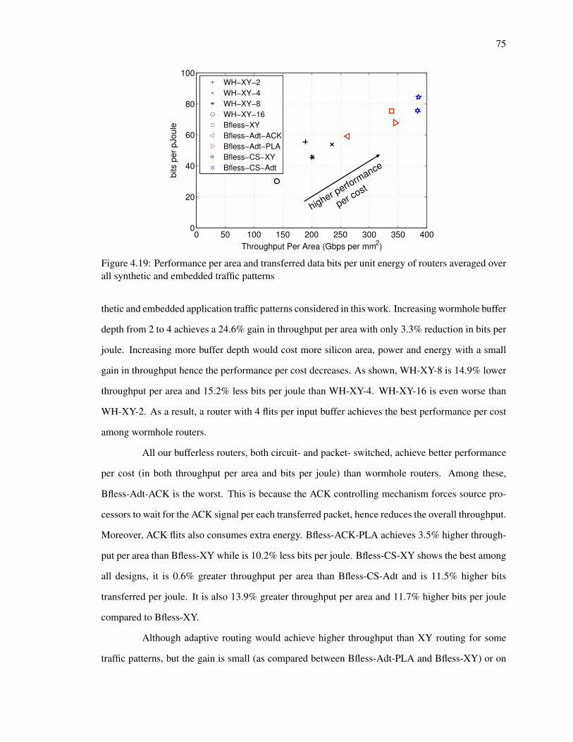
75
0 50 100 150 200 250 300 350 4000
20
40
60
80
100
Throughput Per Area (Gbps per mm2)
bits p
er
pJo
ule
WH−XY−2
WH−XY−4
WH−XY−8
WH−XY−16
Bfless−XY
Bfless−Adt−ACK
Bfless−Adt−PLA
Bfless−CS−XY
Bfless−CS−Adt
higher perfo
rmance
per cost
Figure 4.19: Performance per area and transferred data bits per unit energy of routers averaged over
all synthetic and embedded traffic patterns
thetic and embedded application traffic patterns considered in this work. Increasing wormhole buffer
depth from 2 to 4 achieves a 24.6% gain in throughput per area with only 3.3% reduction in bits per
joule. Increasing more buffer depth would cost more silicon area, power and energy with a small
gain in throughput hence the performance per cost decreases. As shown, WH-XY-8 is 14.9% lower
throughput per area and 15.2% less bits per joule than WH-XY-4. WH-XY-16 is even worse than
WH-XY-2. As a result, a router with 4 flits per input buffer achieves the best performance per cost
among wormhole routers.
All our bufferless routers, both circuit- and packet- switched, achieve better performance
per cost (in both throughput per area and bits per joule) than wormhole routers. Among these,
Bfless-Adt-ACK is the worst. This is because the ACK controlling mechanism forces source pro-
cessors to wait for the ACK signal per each transferred packet, hence reduces the overall throughput.
Moreover, ACK flits also consumes extra energy. Bfless-ACK-PLA achieves 3.5% higher through-
put per area than Bfless-XY while is 10.2% less bits per joule. Bfless-CS-XY shows the best among
all designs, it is 0.6% greater throughput per area than Bfless-CS-Adt and is 11.5% higher bits
transferred per joule. It is also 13.9% greater throughput per area and 11.7% higher bits per joule
compared to Bfless-XY.
Although adaptive routing would achieve higher throughput than XY routing for some
traffic patterns, but the gain is small (as compared between Bfless-Adt-PLA and Bfless-XY) or on

76
average is even worse (as compared between Bfless-CS-Adt and Bfless-XY). Moreover, adaptive
routing adds more design complexity which takes more design time and suffers from testing and
verification issues. Therefore, in the overall design trade-offs, we prefer to use simple XY routing
for our bufferless routers so that achieving both low cost, high performance per cost and naturally
guaranteed in-order packet delivery.
4.6 Related Work
High performance router designs attract a large number of approaches such as express
virtual-channel [59], speculative pipelining [57, 58], shared-buffers [88, 99, 113]. In addition, adap-
tive routing algorithms were proposed for gaining more throughput for certain regular traffic pat-
terns [46,47,51,52]. Unfortunately, these designs show two main drawbacks restricting themselves
to be used in practical chips. First, they are highly complex so costly in both silicon area and power.
Second, they do not guarantee delivering packets in-order that add more costs to processors for
reordering these packets before they are able to be consumed. In this work, reversely, we target
minimizing router costs while keeping the achieved performance per unit cost better than traditional
routers.
There are a few contributions addressing the out-of-order delivery problem we found in
the literature. In the work reported by Murali et al. [114], packets are allowed to route on non-
overlap paths between a source-destination pair, but they are forced to wait at input ports of the
destination router. The destination router then picks these packets and delivers them to its processor
in-order. This method, unfortunately, is prone to deadlock due to the limited buffer space at input
ports of routers [115].
In the work by Martinez et al., destination processors drop the out-of order packets and
request the sources to resend them [116]. In the worst case when network congestion is high, the
resent packets could be dropped again, repeatably, which reduce more the overall network perfor-
mance. Dropping and resending packets, obliviously, also consume extra energy.
Palesi et al. proposed to group multiple consecutive packets into a message and force all
packets in a message to travel on the same path to the destination. The source processor is allowed
to send one message and wait until receiving an acknowledge packet from the destination before

77
sending another message. This mechanism ensures packets to arrive the destination in-order [115].
We adopt this idea into our Bfless-Adt-ACK router, however, as shown in our experiments, the
ACK controlling mechanism has low performance while consumes high area, power and energy
compared to a simple XY routing.
Bufferless router design, recently, becomes increasingly attractive as a solution for achiev-
ing low-cost on-chip networks. Due to without buffer for storing incoming data flits, these bufferless
routers utilize a “hot-spot” routing principle which either drops the flit or deflects it to another out-
put port if its desired output port is busy [55, 70, 71]. Dropping flits requires the router to support a
mechanism for noticing the sources to retransmit the dropped packets. Deflecting flits cause flit to
go to non-minimal paths which are potential for deadlock and livelock. Therefore, the routers must
add more complex control logic and prioritized scheduling circuits to avoid these problems. As a re-
sult, these bufferless routers were shown to consume even higher energy than buffered routers [72].
Furthermore, flit dropping and deflecting cause the out-of-order delivery of not only packets but
also the flits of each packet. This adds much more cost and complexity to the reordering buffers at
receiving processors.
Our bufferless routers differ from previous work are that we do not drop or deflect flits.
For bufferless PS routers, we use simple 1-bit fine-grained flow control for input registers so that no
flit overwriting is allowed. Even though this method reduces network throughput, it consumes low
area, power and energy. For bufferless CS routers, only the head flit of each packet is sent for setting
up the path to its destination before the remaining flits of the packet are sent, hence achieving higher
throughput than bufferless PS routers. Only non-minimal routing algorithms (both XY or adaptive)
and simple round-robin arbiters are used hence ensure the network to be livelock free. Furthermore,
all our bufferless routers guarantee delivering packets in-order.
Previous circuit-switched router designs utilize two separate networks, one for path setup
and one for data transfers [37–39]. Routers on the setup network are buffered for storing multiple
setup packets from different flows for speeding up the average setup time. Obviously, two networks
plus buffers are costly in both silicon area, wiring and power. Our circuit-switched routers are
bufferless with setup flits and data flits share the same network. Only one setup done bit is used to
notice the source whether the path is ready. Sharing only one network for both setup and data flits
in our bufferless circuit-switched routers allows achieving lower design cost and energy with small

78
effect on performance which translates to higher performance per unit cost compared to buffered
routers.
4.7 Summary
High fabrication cost at modern CMOS technologies along with limited chip power bud-
gets favor designs with low area and power costs for systems on chip and also for the networks
connecting processing elements in these systems. Besides that, to achieve the best designs we must
take into account not only the costs but also their offering performance and the trade-offs among
them. Therefore, the achieved performance per unit cost is one of key metrics for comparison among
routers of on-chip networks.
We have presented a set of five low-cost bufferless router designs with guaranteed in-order
packet delivery so that they allow eliminating the need of costly and complex reordering buffers in
processors. The designs cover both circuit-switching and packet-switching techniques. Compared
to traditional buffered wormhole routers, bufferless routers have much lower area and power with
higher throughput per area and lower energy dissipated per bit. Among bufferless routers, circuit-
switched routers achieve higher performance per cost than packet-switched routers. Throughout
our experiments, XY-routing routers show better in the trade-off between performance and cost
than adaptive routing routers averaged over several traffic patterns.

79
Chapter 5
A Reconfigurable Source-Synchronous
On-Chip Network for GALS Many-Core
Platforms
For practical digital designs, clock distribution becomes a critical part of the design pro-
cess for any high performance chip [74]. Designing a global clock tree for a large chip becomes
very complicated and it can consume a significant portion of the power budget, which can be up to
40% of the whole chip’s power [4]. One effective method to address this issue is through the use
of globally-asynchronous locally-synchronous (GALS) architectures where the chip is partitioned
into multiple independent frequency domains. Each domain is clocked synchronously while inter-
domain communication is achieved through specific interconnect techniques and circuits [75]. Due
to its flexible portability and “transparent” features regardless of the differences among computa-
tional cores, GALS interconnect architecture becomes a top candidate for multi- and many-core
chips that wish to do away with complex global clock distribution networks [117]. In addition,
GALS allows the possibility of fine-grained power reduction through frequency and voltage scal-
ing [10].
The outline of this chapter is organized as follows. Section 5.1 explains our motivation
for designing a GALS many-core platform for DSP applications. Design of a reconfigurable source-
synchronous interconnection network is described in Section 5.2. In this section, we also derive a

80
theoretical model for analyzing the throughput and latency of interconnect paths established from
the network. The design of an example many-core DSP platform fabricated in 65 nm CMOS utiliz-
ing this network architecture is shown in Section 5.3. This section also shows the implementation
and measurement results of the chip. Section 5.4 reviews related work and, finally, Section 5.5
concludes the chapter.
5.1 Motivation For A GALS Many-Core Platform
5.1.1 High Performance with Many-Core Design
Pollack’s Rule states that performance increase of an architecture is roughly proportional
to the square root of its complexity [10]. This rule implies that if we apply sophisticated techniques
to a single processor and double its logic area, we speedup its performance by only around 40%. On
the other hand, with the same area increase, a dual-core design using two identical cores could
achieve a 2× improvement assuming that applications are 100% parallelizable. With the same
argument, a design with many small cores should have more performance than one with few large
cores for the same die area. However, performance increase is heavily hindered by Amdahl’s Law,
which implies that this speedup is strictly dependent on the application’s inherent parallelism:
Speedup ≈1
(1 − Parallel%) + 1N· Parallel%
(5.1)
where N is the number of cores.
Fortunately, for most applications in the DSP and embedded domain, a high degree of
task-level parallelism can be easily exposed [118] through their task-graph representatives such
as a complete 802.11a baseband receiver shown in Fig. 5.1. By partitioning the natural task-graph
description of a DSP application, where each task can easily fit into one or few small processors, the
complete application will run much more efficiently. This is due to the elimination of unnecessary
memory fetching and complex pipeline overheads [119]. In addition, the tasks themselves run in
tandem like coarse pipeline stages.

81
Frame
DetectionTiming
Synch.
CFO
Estimation
CFO
Compen.
Guard
Removal64-pt FFT
Subcarrier
Reordering
Channel
Estimation
Channel
Equalizer
Constell.
De-
mapping
De-
interleav.
Step 1
De-
interleav.
Step 2
De-
puncturing
SIGNAL
decoding
De-
scrambl.
Pad
Removal
from ADC
to MAC layer
Auto-
correlation
Signal
Energy
Comput.
Data
Dist.
Viterbi
Decoder
Acc. CFO
Vector
Post
Timing
Synch.
Figure 5.1: Task-interconnect graph of an 802.11a WLAN baseband receiver. The dark lines repre-
sent critical data interconnects.
5.1.2 Advantages of the GALS Clocking Style
Since each core operates in its own frequency domain, we are able to reduce the power
dissipation, increase energy efficiency and compensate for some circuit variations on a fine-grained
level as illustrated in Fig. 5.2:
• GALS clocking design with a simple local ring oscillator for each core eliminates the need
for complex and power hungry global clock trees.
• Unused cores can be effectively disconnected by power gating, and thus reducing leakage.
• When workloads distributed for cores are not identical, we can allocate different clock fre-
quencies and supply voltages for these cores either statically or dynamically. This allows the
total system to consume a lower power than if all active cores had been operating at a single
frequency and supply voltage [120].
• We can reduce more power by architecture-driven methods such as parallelizing or pipelining
a serial algorithm over multiple cores [121].
• We can also spread computationally intensive workloads around the chip to eliminate hot

82
Accelerator
1
Shared MemoryAccelerator
3
Accelerator 2
Figure 5.2: Illustration of a GALS many-core heterogeneous system consisting of many small iden-
tical processors, dedicated-purpose accelerators and shared memory modules running at different
frequencies and voltages or fully turned off.
spots and balance temperature.
• GALS design flexibility supports remapping or adjusting frequencies of processors in an ap-
plication that allows it to continue working well even under the impact of variations.
From these advantages in both performance and power consumption, many-core GALS
style is highly desirable for designing programmable/reconfigurable DSP computational platforms [122].
However, the challenge now is how to design a low area and power cost interconnect network that is
able to offer low latency and high communication bandwidth for these GALS many-core platforms.
Next section describes our proposed reconfigurable network utilizing a novel source-synchronous
clocking scheme for tackling this challenge.
5.2 Design and Evaluation of a Reconfigurable GALS-Compatible Source-
Synchronous On-Chip Network
The static characteristic of interconnects in the task-graphs of DSP and embedded appli-
cations motivates us to build a reconfigurable circuit-switched network for our many-core platform.
The network is configured before run-time to establish static interconnects between any two proces-

83
Processor
Core
Osc
Switch
FIFO
We
st
South
East
North
Figure 5.3: The many-core platform from Fig. 5.2 with switches inside each processor that can
establish interconnects among processors in a reconfigurable circuit-switched scheme.
. . .
Switch A Switch B
driver wire
Cor
e
We
st
South
Ea
st
North
(b)(a)
Figure 5.4: (a) A unidirectional link between two nearest-neighbor switches includes wires con-
nected in parallel. Each wire is driven by a driver consisting of cascaded inverters. (b) A simple
switch architecture consisting of only five 4-input multiplexers.
sors described by the graph. Due to its advantages compared to clockless handshaking techniques
as explained in Chapter 2, the source-synchronous communication technique is utilized in our in-
terconnect networks for transferring data across clock domains in our GALS array of processors.
This section presents the design of our reconfigurable interconnection network; and also describes
how inter-processor interconnects are configured. Evaluation of throughput and latency of these in-
terconnects are given through formulations developed from timing constraints combined with delay
values obtained from SPICE models.
5.2.1 Architecture of Reconfigurable Interconnection Network
Figure 5.3 shows the targeted GALS many-core platform from Fig. 5.2 but focuses on its
interconnect architecture. Processors are interconnected by a static 2-D mesh network of reconfig-

84
Proc. B
Core
Osc
FIFO
Proc. A
Core
Osc
FIFO
Proc. C
Core
Osc
FIFO
Link
PathSwitch
Proc. D
Core
Osc
FIFO
clock
data
valid
full
Figure 5.5: Illustration of a long-distance interconnect path between two processors directly through
intermediate switches. On this interconnect, data are sent with the clock from the source processor
to the destination processor.
urable switches. Each switch connects with its nearest neighboring switch by two unidirectional
links where each link is composed of metal wires in parallel as depicted in Fig. 5.4(a); one wire per
data bit. Each wire is driven by a cascade of inverters that are appropriately sized. An intercon-
nect path between any two processors is formed from one or many links connecting intermediate
switches.
We will investigate the throughput and latency of interconnects that are configured from
switches with the architecture consisting of only 4-input multiplexers as shown in Fig. 5.4(b). The
switch has five ports: the Core port which is connected to its local core, and the North, South, West,
and East ports which are connected to its four nearest neighbor switches. As shown in the figure,
an input from the West port can be configured to go out to any port among the Core, North, South,
East ports and vice versa. For simplicity, we only shows its full connections to and from the West
port; all the other ports are connected in a similar fashion.
Figure 5.5 illustrates an example of a long-distance interconnection from Proc. A to Proc.
D passing through two intermediate processors B and C. This interconnection is established by
configuring the multiplexers in the switches of these four processors. The configuration is done
pre-runtime which fixes this communication path; thus, this static circuit-switched interconnect

85
source clock
FIFOsource data dest. data
dest. clock
output register
Proc. DProc. BProc. A
input dual-clock FIFO
Proc. C
N bits N wires
switch
clock buffer
Figure 5.6: A simplified view of the interconnect path shown in Fig. 5.5
is guaranteed to be independent and never shared. So long as the destination processor’s FIFO
is not full, a very high throughput of one data word per cycle can be sustained. This compares
favorably to a packet-switched network whose runtime network congestion can significantly degrade
communication performance [59, 87].
On this interconnect path, the source processor (Proc. A) sends its data along with its
clock to the destination. The destination processor (Proc. D) uses a dual-clock FIFO to buffer the re-
ceived data before processing. Its FIFO’s write port is clocked by the source clock of Proc. A, while
its read port is clocked by its own oscillator, and thus supports GALS communication. Storage ele-
ments inside the FIFO can be an SRAM array [41,123] or a set of flip-flop registers [87,124]. Data
sent on this interconnect path will pass through four multiplexers (of four corresponding switches)
and three switch-to-switch links as shown in Fig. 5.6. These switches are not only responsible for
routing data on the links but also act as repeaters along the long path when combined with wire
drivers.
5.2.2 Approach Methodology
Evaluation of the characteristics of these reconfigurable interconnects are based on the
delay values simulated by HSPICE. Simulation setups were performed through the use of CMOS
technology cards given by the Predictable Technology Model (PTM) [125]. For analyzing the effect
of technology scaling on interconnect performance, we ran simulations on five technology nodes:
90 nm, 65 nm, 45 nm, 32 nm and 22 nm. The wire dimensions used for simulations were derived
from the reports of the International Technology Roadmap for Semiconductors (ITRS) [126].

86
Upper Layer
Lower Layer
. . . . . .
Cg
Cg
Cc Cc
ws
t
h
Figure 5.7: A side view of three metal layers where the interconnect wires are routed on the middle
layer. Each wire has ground capacitances with upper and lower metal layers and coupling capaci-
tances from adjacent intra-layer wires.
5.2.3 Link and Device Delays
In order to characterize performance of interconnects we firstly consider wires that are
connected between two adjacent switches. These wires are routed on intermediate layers where
the lower layers (metal 1 or 2) are used for intra-cell or inter-cell layouts and the upper layers are
reserved for power distribution and other global signals. In this work, we assume all interconnect
wires are on the same layer and have the same length when connecting two adjacent switches.
An interconnect wire in the intermediate layer incurs both ground and coupling capaci-
tances as depicted in Fig. 5.7. These capacitance values depend on the metal wire dimensions (space
s, width w, thickness t, height h, length l) and the inter-layer dielectric κILD that can be calculated
from formulations proposed by Wong et al. [127]. These formulations are also used by PTM on
their online interconnect tool [128].
Table 5.1 shows the wire dimensions and intra-layer dielectric based on ITRS, that was
used in the work by Im et al. [129], and its calculated resistances and capacitances over many
technology nodes from 90 nm down to 22 nm. The wire length is 2 mm at 90 nm technology
and is scaled correspondingly to each technology node. Notice that the wire length connecting
two adjacent switches approximates the length (or width) of a processor in the platform as seen
in Fig. 5.5. With these simple processors, a 20 mm x 20 mm die (400 mm2) would contain 100
processors at 90 nm and up to 1672 processors at 22 nm.

87
Table 5.1: Dimensions of interconnect wires at the intermediate layer based on ITRS [126] and with
resistance and capacitance calculated by using PTM online tool [128]
Technology (nm) 90 65 45 32 22
width w (nm) 207 147 102 72 50
space s (nm) 222 158 116 81 60
thickness t (nm) 351 264 183 135 98
height h (nm) 309 234 162 121 89
κILD 2.7 2.4 2.1 1.9 1.7
length l (µm) 2000 1444 1000 711 489
Rw (Ω) 556.9 753.8 1084.7 1481.1 2018.4
Cg (fF) 57.7 35.0 21.3 12.9 7.6
Cc (fF) 96.6 65.9 39.8 27.2 17.7
5x 25xRw/3
2Cg/6
Rw/3 Rw/3
2Cg/3 2Cg/3 2Cg/6 CL
5x 25x Cc/6 Cc/3 Cc/3 Cc/6Rw/3
2Cg/6
Rw/3 Rw/3
2Cg/3 2Cg/3 2Cg/6 CL
Cc/6 Cc/3 Cc/3 Cc/65x 25x Rw/3
2Cg/6
Rw/3 Rw/3
2Cg/3 2Cg/3 2Cg/6 CL
. . .. . .
A
B
C
. . .. . .
. . .. . .
. . .. . .
Figure 5.8: Circuit model used to simulate the worst case and best case inter-switch link delay
considering the crosstalk effect between adjacent wires. Wires are simulated using a Π3 lumped RC
model.
For estimates of the switch-to-switch link delay while considering the effect of crosstalk
noise due to coupling capacitances, we used the Π3 lumped RC model for setting up wires in
HSPICE. Higher degree models such as Π5 or so on can make the simulation results more accurate
but also slows down the simulation time. The Π3 model was proven to have an error of less than 3%
compared with the accurate value of a distributed RC model [3]. Fig. 5.8 shows our circuit setup for
simulation of wires in an inter-switch link including the coupled capacitances among them1. In this
setup, load capacitance CL is equivalent to the input gate capacitance of a 4-input multiplexer. The
1For more accuracy, we can consider the multi-coupled case that takes into account capacitances coupled with far wires
rather than only adjacent wires [130]. However, the coupled capacitances from far wires are very small in compared with
those from adjacent wires, so their impacts are negligible [131].

88
Dlnsert
Dclkbuff,flip-flop + tclk-q + Dpath,max
Dpath,min + Dclkbuff,FIFO
Dpath,max + Dclkbuff,FIFO
clock @ source processor
data bit @ source processor
clock @ destination input FIFO
data bit @ destination input FIFO
clock @ destination input FIFOafter inserted a delay
Timing uncertainty
Dclkbuff,flip-flop + tclk-q + Dpath,min
safe rising edges
Figure 5.9: Timing waveforms of clock and data signals from the source processor to the destination
FIFO
Table 5.2: Delay values simulated using PTM technology cards
Technology (nm) 90 65 45 32 22
Supply Voltage Vdd (V) 1.20 1.10 1.00 0.90 0.80
Threshold Voltage Vth (V) 0.30 0.28 0.25 0.23 0.20
Dlink,max (ps) 271.8 223.8 142.9 123.1 104.7
Dlink,min (ps) 131.4 102.3 60.5 47.6 38.5
Dclkbu f f , f lip f lop (ps) 37.0 27.9 13.4 9.4 7.2
Dclkbu f f ,FIFO (ps) 93.2 69.8 25.9 18.2 14.2
Dmux (ps) 48.1 37.7 16.8 13.2 11.3
tsetup (ps) 25.2 20.1 11.0 9.9 7.0
thold (ps) -18.9 -15.1 -5.2 -3.9 -3.1
tclk−q (ps) 104.5 83.8 38.6 23.2 22.1
delay of a circuit is measured from when its input point reaches 0.5Vdd until the output point also
reaches 0.5Vdd.
Due to crosstalk, depending on the data patterns sent on the wires, three cases of delay
are experienced. The nominal delay happens when the signal on a wire goes high while both its
neighboring wires do not change. The best case delay Dlink,min occurs when the signal on a wire
moves in the same direction with its two neighbors; and the worst case delay Dlink,max occurs when
the signal on that wire switches in the opposite direction with its neighbors.
The simulated delay values with respect to each CMOS technology node are given in
Table. 5.2. This table also lists the values of Vdd and threshold voltage Vth used in the simulations.

89
Values of Vdd at each technology node are predicted by Zhao and Cao [125], and those of Vth are
assumed to be 14Vdd [132]. In this table, we also include the delays of clock buffers when driving
a flip-flop stage (Dclkbu f f , f lip f lop), a FIFO (Dclkbu f f ,FIFO) and the delay of a 4-input multiplexer
(Dmux). We simulated a static positive D flip-flop using minimum-size transistors and its setup time
tsetup, hold time thold and propagation delay tclk−q are also shown in the table. A minor note is that
the flip-flop has negative hold time, which means that it can correctly latch the current data value
even when the rising clock edge arrives just after a new transition of data bits.
5.2.4 Interconnect Throughput Evaluation
For an interconnect path between two processors in a distance of n link segments, this
path will travel through n + 1 switches including those of the source and destination processors (as
depicted in Fig. 5.6) that passes through n + 1 multiplexers and n inter-switch links. Therefore, its
minimum (best case) and maximum (worst case) delays are:
Dpath,min = n · Dlink,min + (n + 1)Dmux (5.2)
and
Dpath,max = n · Dlink,max + (n + 1)Dmux (5.3)
Figure 5.9 shows timing waveforms of the clock and corresponding data sent from a
source to its destination. Data bits are sent at the rising edge of the source clock and each bit
is only valid in one cycle. Both clock and data bits travel in the same manner on the configured
interconnect path and therefore have the same timing uncertainty with a small delay difference: the
clock signal has to pass through a clock buffer before driving the destination FIFO while the data
signal has a clock buffer delay at the output register of the source processor and a tclk−q delay before
traveling on the interconnect path.
As seen in the figure, due to the timing uncertainty of both clock and data signals, metasta-
bility can occur at the input of destination FIFO when they transit at almost same time. For safety,
we have purposely inserted a delay line on the clock signal before it drives the destination FIFO (as
shown in Fig. 5.10), effectively moving the rising clock edge into the stable window between two
edges of the data bits as depicted in the last waveform of Fig. 5.9. The value of the inserted delay

90
source clock
FIFOsource data dest. data
dest. clock
inserted delay
Figure 5.10: Interconnect circuit path with a delay line inserted in the clock signal path before the
destination FIFO to shift the rising clock edge to a stable data window
Dinsert must satisfy the setup time constraint:
Dinsert + nDlink,min + (n + 1)Dmux + Dclkbu f f ,FIFO
> Dclkbu f f , f lip f lop + tclk−q + nDlink,max + (n + 1)Dmux + tsetup
or
Dinsert > n(Dlink,max − Dlink,min) + Dclkbu f f , f lip f lop − Dclkbu f f ,FIFO
+ tsetup + tclk−q
(5.4)
Given a delay value Dinsert satisfying the above condition, the period of source clock used
on the interconnect also has to meet the hold time constraint:
Dinsert + Dclkbu f f ,FIFO + nDlink,max + (n + 1)Dmux + thold
< Dclkbu f f , f lip f lop + tclk−q + nDlink,min + (n + 1)Dmux + Tclk
and therefore,
Tclk > n(Dlink,max − Dlink,min) + Dinsert
+ Dclkbu f f ,FIFO − Dclkbu f f , f lip f lop + thold − tclk−q
(5.5)
The minimum clock period strongly depends on the timing uncertainty (Dlink,max−Dlink,min)
and linearly increases with the interconnect distance n. The maximum frequency (corresponding to
the minimum period) of source clock used for transferring data on an interconnect path correspond-
ing to a distance is given in Fig. 5.11. When connecting two nearest neighboring processors, the
interconnect can run at up to 3.5 GHz at 90 nm and up to 7.3 GHz at 22 nm. The maximum
frequency is inversely proportional to n that reduces when interconnect distance increases.
5.2.5 Interconnect Latency
Latency of an interconnect path is defined as the time at which a data word is sent by the
source processor until it is written to the input FIFO of the destination processor. The data travels

91
0 1 2 4 6 8 10 12 14 16 18 200
1
2
3
4
5
6
7
8
Interconnect Distance (number of inter−switch links)
Ma
x F
req
ue
ncy (
GH
z)
@ 90 nm
@ 65 nm
@ 45 nm
@ 32 nm
@ 22 nm
Figure 5.11: Maximum frequency of the source clock over various interconnection distances and
CMOS technology nodes
along the path, and then registered at the destination FIFO. This path includes both delays by the
inserted delay line and clock buffer on the clock signal and also a flip-flop propagation delay tclk−q.
Therefore, the maximum latency of an interconnect path with distance of n inter-switch links is
given by:
Dconnect,max = nDlink,max + (n + 1)Dmux + Dinsert + Dclkbu f f ,FIFO + tclk−q (5.6)
The maximum absolute latency (in ns) corresponding to distance is plotted in Fig. 5.12.
Consider a nearest neighboring interconnect, which has less than 1 ns latency regardless of the
technology used. This means that at 1 GHz the interconnect latency is less than 1 cycle, and at
500 MHz latency is less than a half of cycle.
The maximum number of clock cycles that the data will travel on an interconnect distance
is given in Fig. 5.13. This maximum clock cycle latency is equal to the maximum latency (in ns)
multiplied by the maximum clock frequency (in GHz) at that distance. Interestingly, the latency
cycles even decreases when distance increases. This happens because the clock period is larger for
longer distances. In all cases, the latency is less than 2.5 cycles at 90 nm and less than 1.7 cycles at
22 nm regardless of distance. These latencies are very low when compared with dynamic packet-
switched networks whose latency (in cycles) is proportional to the distance, which can be very high
if routers are pipelined into many stages.

92
0 1 2 4 6 8 10 12 14 16 18 200
1
2
3
4
5
6
7
8
9
10
Interconnect Distance (number of inter−switch links)
Ma
x A
bso
lute
La
ten
cy (
ns)
@ 90 nm
@ 65 nm
@ 45 nm
@ 32 nm
@ 22 nm
Figure 5.12: Maximum interconnect latency (in ns) over various distances
5.2.6 Discussion
Our interconnects can guarantee an ideal throughput of one data word per cycle because
no network contention occurs, while also achieving very low latency of only a few cycles. Further-
more, our interconnect architecture well supports GALS scheme while does not require complicated
control circuits and buffers at switches along the interconnect path; therefore, it is also highly effi-
cient in terms of area and power consumption. The network circuit occupies only 7% of each pro-
grammable processor’s area2 and only consumes 10% of the total power while mapping a complex
application as shown in Section 6.2. These advantages along with the deterministic characteristic
of interconnects in DSP applications we are targeting support the idea of building a reconfigurable
circuit-switched network for our platform.
However, these advantages come with a cost of sacrificing the flexibility and interconnect
capacity. Programmer (under the help of automatic tools) must setup all interconnects before an
application can run. In addition, the number of interconnect links are limited and interconnects
after configured are not shared; therefore, for some complex applications, it is difficult for setting
up all connects or even there are not enough links required [133]. For increasing the interconnect
capacity, the platform is equipped with two static configurable networks as will be described in
Section 5.3.2.
2Note that this area is sum of two static networks, so each network occupies only 3.5% of the processor’s area.

93
0 1 2 4 6 8 10 12 14 16 18 201
1.5
2
2.5
3
Interconnect Distance (number of inter−switch links)
Ma
x L
ate
ncy (
cycle
s)
at
the
Ma
x F
req
.
@ 90 nm
@ 65 nm
@ 45 nm
@ 32 nm
@ 22 nm
Figure 5.13: Maximum communication latency in term of cycles at the maximum clock frequency
over interconnect distances
5.3 An Example GALS Many-core Platform: AsAP2
The top level block diagram of our 167-processor computational platform (AsAP2) is
shown in Fig. 5.14. The platform consists of 164 small programmable processors, three accelerators
(FFT, Viterbi decoder and Motion Estimation), and three 16 KB shared memory modules [13].
Placement of the three accelerators and the three shared memories at the bottom of the array was
chosen only to simplify the routing of global configuration signal wires and to simplify mapping
of applications onto the large central homogeneous array (as opposed to breaking up the array by
placing accelerators or memories in the middle) [134].
Because of the array nature of the platform, the local oscillator, voltage switching, config-
uration and communication circuits are reused throughout the platform. These common components
are designed as a generic “wrapper” which could then be reused to make any computational core
compatible with the GALS array, and thus facilitates easy design enhancements. The difference be-
tween the programmable processors and the accelerators is mainly in their computational datapaths
as illustrated in Fig. 5.15. The programmable processors have an in-order single-issue 16-bit fixed
point datapath, with a 128×16-bit DMEM, a 128×35-bit IMEM, two 64×16-bit dual-clock FIFOs,
and they can execute 60 basic ALU, MAC, and branch type instructions.

94
input data,valid and
clock
output data, valid and
clock
output request
Configuration and Test Logicinputmux
select
output mux
select
serial configuration bit-stream test out
input request
to analogpadsMotion
Estimation
Viterbi
Decoder FFT
16 KB Shared Memories
Figure 5.14: Block diagram of the 167-processor computational platform (AsAP2) [13]
5.3.1 Per-Processor Clock Frequency and Supply Voltage Configuration
All processors, accelerators and memory modules operate at their own fully-independent
clock frequency that is generated by a local clock oscillator and is able to arbitrarily halt, restart, and
change frequency. During run-time, processors fully halt their clock oscillator six cycles after there
is no work to do (for finishing all instructions already in the pipeline), and they restart immediately
once work becomes available. Each ring oscillator supports frequencies between 4.55 MHz and
1.71 GHz with a resolution of less than 1 MHz [13]. Off-chip testing is used to determine the valid
operational frequency settings for the ring oscillator of each processor, which takes into account
process variations.
The platform is powered by two independent power grids which will in general, have
different supply voltages. Processors may also be completely disconnected from either power grid
when they are unused. The benefits of having more than two supply voltages are small when com-
pared to the increased area and complexity of the controller needed to effectively handle voltage
switching [135]. Using two supply voltages for power management was also employed in the

95
COREDatapath
Osc.
Switch
Supply Voltages
Controller
Figure 5.15: Simplified block diagram of processors or accelerators in the proposed heterogeneous
system. Processor tiles are virtually identical, differing only in their computational core.
ALPIN test chip [136].
Although the processors have hardware to support dynamic voltage and frequency scaling
(DVFS) through software or a local DVFS controller [13, 137], dynamic analyses are much more
complex and do not demonstrate the pure frequency and voltage gains as clearly as with static
assignments. In addition, due to its control overhead, an application running in a DVFS mode may
actually dissipate more power if the workload is predictable pre-runtime and is relatively static.
Data and analysis throughout this work utilizes clock frequencies and supply voltages that
are kept constant throughout workload processing. Static configuration is intentionally set by the
programmer for a specific application to optimize its performance and power consumption. This
method is especially useful for applications that have a relatively static load behavior at run-time.
The frequency and supply voltage of each processor are controlled by its VFC that is depicted in
Fig. 5.16.
The VFC and communication circuits operate on their own supply voltage that is shared
among all processors in the platform to guarantee the same voltage level for all interconnect links,
thus avoiding the use of level shifters between switches.

96
Volt. &
Freq.
Controller
VddHigh
VddCore
VddAlwaysOn
control_freq
VddOsc
control_high
control_low
VddLow
GndCom
GndOsc
Switch
Oscconfig signals
from core
Figure 5.16: The Voltage and Frequency Controller (VFC) architecture
5.3.2 Source-Synchronous Interconnection Network
All processors in the platform are interconnected using a reconfigurable source-synchronous
interconnect network as described in Section 5.2. To increase the interconnect capacity, each pro-
cessor has two switches as depicted in Fig. 5.17 and, correspondingly, has two dual-clock FIFOs –
each per switch (on the output of its Core port). These switches connect to their nearest neighboring
switches to form two separate 2-D mesh networks; simplifying the mapping job for programmers.
Processor
Core
Osc
FIFO
Switch
Processor
Core
Osc
Switch
FIFO
Figure 5.17: Each processor tile contains two switches for the two parallel but separate networks

97
Furthermore, two networks naturally support tasks that need two input channels3.
A reconfigurable delay line is inserted on the clock signal before each FIFO to adjust its
delay value for matching with its corresponding data. The reconfigurable delay line is a simple
circuit including many delay elements and configured by multiplexers for setting a delay value. The
delay value is chosen corresponding to the interconnect distance for satisfying constraint (4). For
interconnects of a mapped application, their distances are known; therefore the corresponding delay
values are statically set. Thanks to these static settings, the delay circuits do not cause any glitch on
the clock signals at run-time.
5.3.3 Platform Configuration, Programming and Testability
For array configuration (e.g. circuit-switch link configurations, VFC settings, etc.), the
compiler, assembler and mapping tools place programs and configurations into a bit-stream that
is sent over a Serial Peripheral Interface (SPI) into the array as depicted at top of Fig. 5.14. This
technique needs only a few I/O pins for chip configuration. The configuration information and
instructions as well as address of each processor are sent into the chip in a serial manner bit by bit
along with an off-chip clock. Based on the configuration code, each processor will set its frequency
and voltage; and the multiplexers and delay lines of its switches are also configured for establishing
communication paths.
Our current test chip employs a simple test architecture for functional testing only that
determines whether a processor operates correctly. Test outputs of all processors share the same
the ”test out” pins as shown at the top of Fig. 5.14. Therefore, there is only one processor that
can be tested at a time, but this can be easily reconfigured by an off-chip test environment with
test equipment (e.g. logic analyzer). Test signals include all key internal control and data values.
Our current test architecture works well at the processor level that is acceptable for a research chip.
High-volume manufacturing would require the addition of special circuits (e.g. scan path) for rapid
high-fault-coverage testing [138, 139].

98
• 65 nm STMicroelectronics
1.19 GHz, 1.3 V
66 MHz, 0.675 V
1.095 GHz, 1.3V
@
5.9
39
mm
410 m
410
m
FFTVit
Mot.
Est. MemMem
5.516 mm
Mem
Figure 5.18: Die micrograph of the 167-processor AsAP2 chip
5.3.4 Chip Implementation
The platform was fabricated in ST Microelectronics 65 nm low-leakage CMOS process
using a standard-cell design flow. Its die micrograph is shown in Fig. 5.18. It has a total of 55
million transistors with an area of 39.4 mm2. Each programmable processor occupies 0.17 mm2,
with its communication circuit occupying 7%, including the two switches, wires and buffers. The
area of the FFT, motion estimation and Viterbi decoder accelerators is six times, four times and one
time, respectively, that of one processor; the memory module is two times the size of one processor.
5.3.5 Measurement Results
We tested all processors in the platform to measure their maximum operating frequencies.
The maximum frequency is obtained once a higher frequency makes outputs of the corresponding
processor incorrect. The maximum frequency and power consumption of the programmable proces-
sors versus supply voltage is shown in Fig. 5.19. As shown in the figure, they have a nearly linear
and quadratic dependence on the supply voltage, respectively. These important characteristics are
used to reduce power consumption of an application by appropriately choosing the clock frequency
3For tasks need more than two input channels, it is easy to use some intermediate processors for collecting and
converting these inputs into two channels.

99
0.6 0.7 0.8 0.9 1.0 1.1 1.2 1.30
200
400
600
800
1000
1200
Supply Voltage (V)
Ma
x F
req
ue
ncy (
MH
z)
Po
we
r (m
W)
0
10
20
30
40
50
60
Figure 5.19: Maximum clock frequency and 100%-active power dissipation of one programmable
processor over various supply voltages
Table 5.3: Average power consumption measured at 0.95 V and 594 MHz
Operation of 100% Active (mW) Stall (mW) Standby (mW)
Processor 17.6 8.7 0.031
FFT 12.7 7.3 0.329
Viterbi 6.2 4.1 0.153
FIFO Rd/Wr 1.9 0.7 ∼0
Switch + Link 1.1 0.5 ∼0
and supply voltage for each processor as detailed in Section 6.2. At 1.3 V, the programmable pro-
cessors can operate up to 1.2 GHz. The configurable FFT and Viterbi processors can run up to
866 MHz and 894 MHz respectively [140].
The maximum frequency of each processor should vary under the impact of process and
temperature variations. Unfortunately, these measurements have not yet been made. Currently, we
can guarantee the correct operation of the mapped application by allowing a frequency margin of
10%-15% of the maximum frequency measured under typical conditions, for each processor.
Table 5.3 shows the average power dissipation of processor, accelerators and communica-
tion circuit at 0.95 V and 594 MHz. This supply voltage and clock frequency is used to evaluate and
test the 802.11a baseband receiver application described in the next section. The FFT is configured
to perform 64-point transformations, and the Viterbi is configured to decode 1/2-rate convolution
codes. The table also shows that during stalls (i.e. non-operation while the clock is active) the

100
0 1 2 3 4 5 6 7 8 9 10 11 12 130
100
200
300
400
500
600
700
800
900
1000
1100
1200
1300
1400
Interconnect Distance (number of inter−switch links)
Ma
x C
lock F
req
ue
ncy (
MH
z)
Figure 5.20: Measured maximum clock frequencies for interconnect between processors over var-
ious interconnect distances at 1.3 V. An Interconnect Distance of one corresponds to adjacent
processors.
processors consume a significant portion, approximately 35-55%, of their normal operating power.
Leakage power are very small while processors are in the standby mode with the clock halted.
Figure 5.20 plots measured data for maximum allowable source clock frequencies when
sending data over a range of interconnect distances at 1.3 V. Interestingly, the measured data has
a similar trend as the theoretically developed model depicted in Fig. 5.11. The differences are
due to the assumptions used in the theoretical model versus the real test chip such as wire and
device parameters. For the model we assumed wires have the same length and are on the same
metal layer with devices modeled from the PTM SPICE cards; while the test chip is built from ST
Microelectronics standard cells with wires that are automatically routed along with buffers that are
added by Cadence Encounter place and route tool. Besides that, environment parameters, process
variation and power supply noise on the real chip add more to these differences. However, the
maximum clock frequency strongly depends on the timing uncertainty of clock and data signals
that linearly increases following the distance; so both measured and theoretical results come to the
same conclusions. Note that, as shown in the figure, because the maximum operating frequency of
processors is 1.2 GHz, source-synchronous interconnects with distances of one and two inter-switch
links also only run up to 1.2 GHz.
The clock frequency of the source processor reduces corresponding to the interconnect
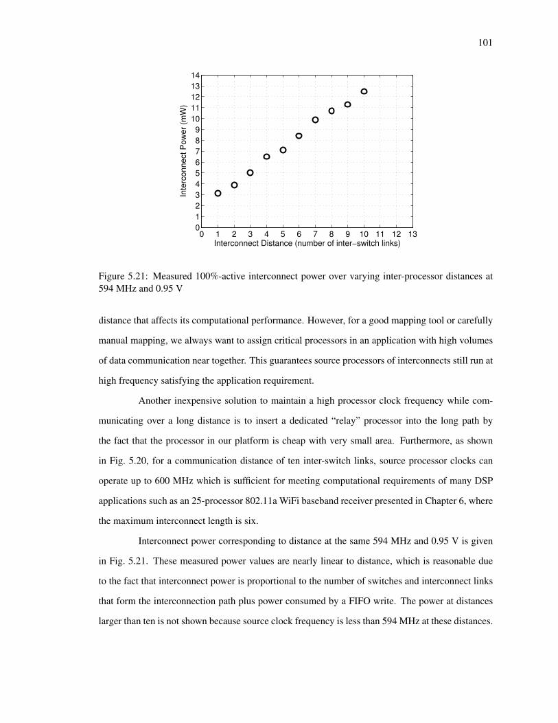
101
0 1 2 3 4 5 6 7 8 9 10 11 12 130
1
2
3
4
5
6
7
8
9
10
11
12
13
14
Interconnect Distance (number of inter−switch links)
Inte
rco
nn
ect
Po
we
r (m
W)
Figure 5.21: Measured 100%-active interconnect power over varying inter-processor distances at
594 MHz and 0.95 V
distance that affects its computational performance. However, for a good mapping tool or carefully
manual mapping, we always want to assign critical processors in an application with high volumes
of data communication near together. This guarantees source processors of interconnects still run at
high frequency satisfying the application requirement.
Another inexpensive solution to maintain a high processor clock frequency while com-
municating over a long distance is to insert a dedicated “relay” processor into the long path by
the fact that the processor in our platform is cheap with very small area. Furthermore, as shown
in Fig. 5.20, for a communication distance of ten inter-switch links, source processor clocks can
operate up to 600 MHz which is sufficient for meeting computational requirements of many DSP
applications such as an 25-processor 802.11a WiFi baseband receiver presented in Chapter 6, where
the maximum interconnect length is six.
Interconnect power corresponding to distance at the same 594 MHz and 0.95 V is given
in Fig. 5.21. These measured power values are nearly linear to distance, which is reasonable due
to the fact that interconnect power is proportional to the number of switches and interconnect links
that form the interconnection path plus power consumed by a FIFO write. The power at distances
larger than ten is not shown because source clock frequency is less than 594 MHz at these distances.

102
5.4 Related Work
The methodology of inter-domain communication is a crucial design point for GALS ar-
chitectures. One approach is the purely asynchronous clockless handshaking, that uses multiple
phases (normally two or four phases) of exchanging control signals (request and ack) for trans-
ferring data words across clock domains [76, 77]. Unfortunately, these asynchronous handshaking
techniques are complex and use unconventional circuits (such as the Muller C-element [3]) typically
unavailable in generic standard cell libraries. Besides that, because the arrival times of events are
arbitrary without a reference timing signal, their activities are difficult to verify in traditional digital
CAD design flows.
The so-called delay-insensitive interconnection method extends clockless handshaking
techniques by using coding techniques such as dual-rail or 1-of-4 to avoid the requirement of delay
matching between data bits and control signals [78]. These circuits also require specific cells that
do not exist in common ASIC design libraries. Quinton et al. implemented a delay-insensitive
asynchronous interconnect network using only digital standard cells; however, the final circuit has
large area and energy costs [79].
Another asynchronous interconnect technique uses a pausible or stretchable clock where
the rising edge of the receiving clock is paused following the requirements of the control signals
from the sender. This makes the synchronizer at the receiver wait until the data signals stabilize
before sampling [80, 81]. The receiving clock is artificial meaning its period can vary cycle by
cycle; so it is not particularly suitable for processing elements with synchronous clocking that need
a stable signal clock in a long enough time. Besides that, this technique is difficult to manage when
applied to a multiport design due to the arbitrary and unpredictable arrival times of multiple input
signals.
An alternative for transferring data across clock domains is the source-synchronous com-
munication technique that was originally proposed for off-chip interconnects. In this approach, the
source clock signal is sent along with the data to the destination. At the destination, the source clock
is used to sample and write the input data into a FIFO queue while the destination clock is used to
read the data from the queue for processing. This method achieves high efficiency by obtaining an
ideal throughput of one data word per source clock cycle with a very simple design that is also sim-

103
ilar to the synchronous design methodology; hence it is easily compatible with common standard
cell design flows [84, 86, 87, 141]. Source-synchronous communication technique was used in our
statically reconfigurable networks presented in this chapter.
5.5 Summary
We have presented a GALS-compatible inter-processor communication network utilizing
a novel source-synchronous interconnection technique allowing efficient communication among
processors which are in different clock domains. The on-chip network is reconfigurable circuit-
switched and is configured before runtime such that interconnect paths can achieve their ideal
throughput at a very low power and area costs. We utilized this network in a high-performance
and energy-efficient programmable DSP platform named AsAP2 consisting of many simple cores
and dedicated-purpose accelerators targeting DSP applications which naturally has a high degree of
task-level parallelism and deterministic inter-task communication traffic.

104
Chapter 6
Application Mapping Case Study:
802.11a Baseband Receiver on AsAP2
In recent years, a wide variety of wireless communication systems has come into widespread
use. To quickly adapt with this variety the flexibility of software-defined radio (SDR) solutions have
become increasingly attractive. Some SDR platforms were proposed and the 802.11a system [142]
is one of the wireless protocols used as benchmarks to evaluate their efficiency.
Some real-time software implementations of the 802.11a baseband transmitter were re-
ported in the literature [96, 143, 144]. The implementations of its receiver, which is much more
complicated, however, either cannot obtain a 54 Mbps throughput [96, 145–147], or ignore some
necessary features such as frame detection/synchronization, carrier frequency offset (CFO) esti-
mation/compensation and channel equalization [148–150]. Speeding up the performance can be
obtained by using some built-in dedicated hardware such as Viterbi decoder and FFT for the core
computational components. However, other processing modules in the system which are imple-
mented in software become bottlenecks that limit the throughput. We eliminate these bottlenecks to
get a complete real-time receiver by exploiting the advantage of task-level parallelism on multiple
small cores of the AsAP2 platform [151] which was presented in Chapter 5.
The remainder of this chapter is organized as follows. Section 6.1 describes the design
of a complete 802.11a baseband receiver. The mapping of this receiver on the AsAP2 platform
is shown in Section 6.2. Section 6.3 describes the evaluation and improvement of the receiver’s

105
Frame Detection / Synchronization
CFO Estimation / Compensation
Guard Removing
FFT
Subcarrier Reordering
Channel Estimation / Equalization
De-modulationDe-interleaving
De-puncturingViterbi
DecodingDescrambing
input samples
output bit sequence
Figure 6.1: Block diagram of a complete 802.11a baseband receiver
S S S S S S S S S S GI2 L L GI SIGNAL . . .
10 short-training symbols 2 long-training symbolswith GI2
Many OFDM data symbols
Data
SIGNALsymbol
8 µs 8 µs 4 µs N x 4 µs
GI
Figure 6.2: Structure of a received frame. S: 16-sample short-training symbol; GI2: 32-sample
double guard interval; L: 64-sample long-training symbol; GI: 16-sample single guard interval;
SIGNAL and DATA fields: 64 samples each.
throughput and power. Section 6.4 reviews and compares related work on software implementation
of the 802.11a receiver on other platforms; and, finally, Section 6.5 summarizes this chapter.
6.1 Architecture of a Complete 802.11a Baseband Receiver
Fig. 6.1 shows the top-level architecture of a complete 802.11a baseband receiver. The
baseband receiver gets signal samples from an analog-to-digital converter (ADC) with a sampling
frequency of 20 MHz. These signal samples form a frame including training symbols and many
OFDM symbols as described in Fig. 6.2.
Ten periodic short-training symbols in the beginning of frame are used for frame detection
and timing synchronization. A common timing metric, which is used for both frame detection and
timing synchronization, was proposed by Schmidl and Cox [152]:
M(n) =|P(n)|2
Q(n)2(6.1)
Where P(n) is the auto-correlation between the received frame and a copy delayed 16

106
−50 0 50 100 150 200 2500
0.2
0.4
0.6
0.8
1
1.2
1.4
index n
M(n
) Thdet
Thsyn
Figure 6.3: Plot of the timing metric M(n) with S NR = 20dB. Thdet and Thsyn are thresholds used
for frame detection and timing synchronization, respectively.
samples from itself. Q(n) is the energy of 16 consecutive samples beginning from the nth sample:
P(n) =
15∑
k=0
r(n + k + 16) · r∗(n + k) (6.2)
Q(n) =
15∑
k=0
|r(n + k)|2 (6.3)
With r(n) is the received samples and (.)∗ denotes the complex conjugate operation.
Since the ten short-training (S) symbols are periodic, under the impact of noise, the timing
metric forms an amplitude plateau as described in Fig. 6.3. This metric begins to increase from the
first S symbol, which then fluctuates around a high amplitude level and then gradually decreases at
the ninth S symbol. This behavior of the timing metrics allows us to easily set constant threshold
values for frame detection and synchronization.
A frame should be detected if its timing metric is larger than a threshold Thdet at some
consecutive samples (we choose the number of these samples to be 48, which equals the number of
samples of 3 S symbols). After the frame is detected, the timing is synchronized by locate the first
sample of the timing metric M(n) which is less than the threshold Thsyn. This sample is the first

107
−1.5 −1 −0.5 0 0.5 1 1.5−1.5
−1
−0.5
0
0.5
1
1.5
In−Phase.
Qu
ad
ratu
re
−1.5 −1 −0.5 0 0.5 1 1.5−1.5
−1
−0.5
0
0.5
1
1.5
In−Phase
Qu
ad
ratu
re
(a) (b)
Figure 6.4: The constellation of 16-QAM subcarriers in the frequency domain with ǫ = 10 ppm at
5 GHz: a) without CFO compensation; b) with CFO compensation.
sample of the tenth S symbol which allows us to determine all long-training, SIGNAL and OFDM
symbols in the frame from now on.
Because division is slow, we replace the frame detection’s condition M(n) =|P(n)|2
Q(n)2 >
Thdet and the timing synchronization’s condition M(n) =|P(n)|2
Q(n)2 < Thsyn with:
|P(n)|2 > Thdet · Q(n)2 (6.4)
and
|P(n)|2 < Thsyn · Q(n)2 (6.5)
respectively. In this project, we choose Thdet = 0.75 and Thsyn = 0.15 as results derived by Jimenez
et al. [153] and Tang et al. [154].
Once the timing has been synchronized, the frequency synchronization step begins. Due
to the difference in the frequency between the transmitter and the receiver, there exists a carrier
frequency offset (CFO) between them. This CFO creates a phase error which is accumulated on
every sample of the frame. Even when the CFO is small, the phase error still make subcarriers (in
the frequency domain) rotate far from the standard constellation points as illustrated in Fig. 6.4. This
CFO extremely degrades the accuracy of the receiver which is why the frequency synchronization
step is necessary in a practical receiver.

108
The CFO can be estimated and compensated using two long-training symbols as proposed
by Sourour [155]. The phase error caused by CFO is estimated as follows:
α =1
64· ∠
63∑
k=0
L2(k) · L∗1(k) (6.6)
where L1(k) and L2(k) are kth samples of the received long-training symbol 1 and 2, respectively.
The mth samples beginning from the first sample of symbol L1 is corrected by rotating
at an angle of −(m + 192)α because the first sample of symbol L1 is separated 192 samples from
the first sample of the frame. This rotation is implemented by using the well-known CORDIC
algorithm [156]. The CORDIC algorithm is very convenient to implement on hardware, however,
to get a high rotation accuracy, it requires a large number of iterations which has a large latency if
implemented in software. The large number of cycles needed by the CORDIC algorithm as well
as the high complexity of other algorithms for rotating samples explains why there are only few
of previous software-based works proposing the CFO correction step in their receiver [146, 147].
We overcome this challenge by exploiting the multiple cores of AsAP2 architecture to rotate many
samples in parallel. This increases overall throughput at the cost of using more processors.
After CFO compensation step, the 16-sample GI field of each OFDM symbol are re-
moved, then 64 data samples are transformed to the frequency domain by a 64-point FFT. Next,
subcarriers in the frequency domain must be equalized to eliminate the effects of the communi-
cation channel. The channel’s coefficients are estimated using information of two long-training
symbols. Let L be the long-training symbol known by both the transmitter and receiver, and L1 and
L2 be two long-training symbols rotated by the CFO compensation. The channel coefficient of the
kth subcarrier is estimated as follows:
H(k) =1
2·
L1(k) + L2(k)
L(k)(6.7)
This estimation of channel coefficients is used to equalize the corresponding subcarriers
of all SIGNAL and DATA symbols. For each kth subcarrier S m(k) of the mth symbol, it is equalized
by:
S m(k) =S m(k)
H(k)(6.8)

109
Above, we used two divisions to compute H(k) and S m(k). Since the division is slow, we
should eliminate one at the equalization step by computing:
S m(k) = S m(k) ·C(k) (6.9)
where C(k) is estimated as:
C(k) =1
H(k)=
2L(k)
L1(k) + L2(k)(6.10)
to replace for estimation of H(k) in Eq. 6.7.
After equalization, the subcarriers of OFDM symbols are de-modulated into binary se-
quences and then these binary sequences are de-interleaved, de-punctured, decoded using Viterbi
algorithm and de-scrambled. In the end, the final obtained binary sequence is sent to the Medium
Access Control (MAC) layer. An important note is that the information from the SIGNAL symbol
after decoded will be used to decide the modulation scheme (BPSK, QPSK, 16-QAM or 64-QAM),
interleaving patterns and puncture pattern of the convolution code (1/2, 2/3 or 3/4) for DATA sym-
bols corresponding to the supported bit rates: 6, 9, 12, 18, 24, 36, 48 or 54 Mbps.
6.2 Mapping the 802.11a Baseband Receiver on AsAP2
6.2.1 Programming Methodology
Programming an application on AsAP2 follows three basis steps: 1) Each task of the
application described by its task-graph representative is mapped on one or a few processors or on an
accelerator. These processors are programmed using our simplified C language and are optimized
with assembly codes. 2) Task interconnects are then assigned by a GUI mapping tools or manually
in a configuration file. 3) AsAP’s C compiler combined with the assembler will produce a single bit
file for programming and configuring the array. The hardware platform configuration is then done
as introduced in Section 5.3.3.
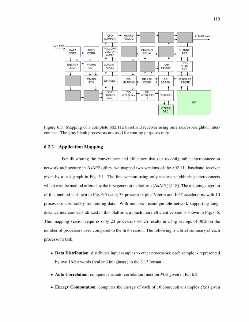
110
DATA
DISTR.
AUTO-
CORR.
ACC. OFF.
VECTOR
COMP.
CFO
COMPEN.
ENERGY
COMP.
FRAME
DET.
CORDIC –
ANGLE
CHANNEL
EQUAL.
CHANNEL
EST.
SUBCARR
. REORD.
TIMING
SYN.CFO EST.
DE-
MAPPING
BR & DL
COMP.
DE-
SCRAM.
PAD
REMOV.
DE-INTERLEAV
1
DE-INTERLEAV
2DE-PUNC.
FFT
VITERBI
DEC.
POST
TIMING
SYN.
to MAC layer
PRE-
CHAN.
EST.
from ADC
GUARD
REMOV.
Figure 6.5: Mapping of a complete 802.11a baseband receiver using only nearest-neighbor inter-
connect. The gray blank processors are used for routing purposes only.
6.2.2 Application Mapping
For illustrating the convenience and efficiency that our reconfigurable interconnection
network architecture in AsAP2 offers, we mapped two versions of the 802.11a baseband receiver
given by a task-graph in Fig. 5.1. The first version using only nearest neighboring interconnects
which was the method offered by the first generation platform (AsAP1) [118]. The mapping diagram
of this method is shown in Fig. 6.5 using 33 processors plus Viterbi and FFT accelerators with 10
processors used solely for routing data. With our new reconfigurable network supporting long-
distance interconnects utilized in this platform, a much more efficient version is shown in Fig. 6.6.
This mapping version requires only 23 processors which results in a big savings of 30% on the
number of processors used compared to the first version. The following is a brief summary of each
processor’s task.
• Data Distribution: distributes input samples to other processors; each sample is represented
by two 16-bit words (real and imaginary) in the 3.13 format.
• Auto Correlation: computes the auto-correlation function P(n) given in Eq. 6.2.
• Energy Computation: computes the energy of each of 16 consecutive samples Q(n) given

111
DATA
DISTR.
AUTO-
CORR.
OFFSET
VECTOR
ACC.
CFO
COMPEN.
ENERGY
COMP.
FRAME
DET.
CORDIC –
ANGLE
CHANNEL
EQUAL.
CHANNEL
EST.
SUBCARR
. REORD.
TIMING
SYN.CFO EST.
DE-
MAPPING
BR & DL
COMP.
DE-
SCRAM.
PAD
REMOV.
DE-INTERLEAV
1
DE-INTERLEAV
2DE-PUNC.
FFT
VITERBI
DEC.
POST
TIMING
SYN.
to MAC layer
PRE-
CHAN.
EST.
: Other Connections (for Control, Detection, Estimation)
: Connections on the Critical Data Path
from ADC
GUARD
REMOV.
DATA
DISTR.
CONTROL
Figure 6.6: Mapping of a complete 802.11a baseband receiver using a reconfigurable network that
supports long-distance interconnects
in Eq. 6.3.
• Frame Detection: detects frame based on the condition of |P(n)|2 > 0.75Q(n)2 in 48 consec-
utive samples.
• Timing Synchronization: locates the first samples that satisfies |P(n)|2 < 0.15Q(n)2 after the
frame was detected.
• Post Timing Synchronization: removes input samples until frame is synchronized.
• Data Distribution Control: controls the distribution of the samples.
• CFO Estimation: computes part ∑63
k=0 L2(k) · L∗1(k) of the carrier frequency offset given in
Eq. 6.6.
• CORDIC Angle: computes angle α given in Eq. 6.6 using the CORDIC algorithm.
• Offset Vector Accumulation: computes the unit vector representing the angle −(m+192)α
which is needed to rotate the mth samples.
• CFO Compensation: rotates samples to compensate for the carrier frequency offset using a
complex multiplication.
• Guard Removal: removes 16 prefix samples of each 80-sample OFDM symbol.

112
• FFT: is FFT accelerator configured to perform a 64-point FFT on 64 samples of each OFDM
symbol.
• Subcarrier Reordering: removes 12 null subcarriers and 4 pilots of each symbol. The re-
maining 48 subcarriers are then reordered as specified in the standard [142].
• Pre-Channel Estimation: computes the average value 12· [L1(k) + L2(k)] for each of 48
subcarriers of two long-training symbols.
• Channel Estimation: computes the channel’s coefficients C(k) given in Eq. 6.10 using the
division algorithm with a small lookup table introduced by Hung et al. [157].
• Channel Equalization: equalizes subcarriers S m(k) as given in Eq. 6.9.
• De-modulation: demaps each subcarrier back into a binary sequence. The number of bits
representing each subcarrier depends on its modulation schemes: 1 bits, 2 bits, 4 bits and 6
bits for BPSK, QPSK, 16-QAM and 64-QAM, respectively.
• Deinterleaving 1 and Deinterleaving 2: are two deinterleaving steps that reverse the inter-
leaving steps from the transmitter.
• Depuncturing: inserts dummy bits into the locations removed by the convolution encoder of
the transmitter for creating code rate 2/3 and 3/4 from the code rate 1/2.
• Viterbi Decoding: is a built-in accelerator used to decode the bit sequence using Viterbi
algorithm.
• Descrambling: de-scrambles the decoded bit sequence using the generator polynomial G(x) =
x7+ x4+ 1.
• Bit Rate & Data Length Computation: retrieves information about bit rate and data length
from the decoded SIGNAL symbol. The bit rate tells information about the modulation
scheme and code rate of the convolution code. This information is used to control the De-
modulation, Interleaving 1, Interleaving 2 and Depuncturing processors. The data length tells
the number of useful data bytes contained in the received frame.

113
• Pad Removal: removes garbage bits which include the Tail and Pad bits before sending the
final bit sequence to the MAC layer.
The receiver mapped is complete and includes all the necessary practical features such
as frame detection and timing synchronization, carrier frequency offset (CFO) estimation and com-
pensation, and channel estimation and equalization. In this implementation, the CFO compensation
uses a lookup table to compute the complex unit vector of the accumulated offset angle, and then
uses a complex multiplication for sample rotation instead of using the CORDIC algorithm as re-
ported in our previous work [94] (all other processors are unchanged).
The compiled code of the whole receiver is simulated on the Verilog RTL model of our
platform using Cadence NCVerilog and its results are compared with a Matlab model to guarantee
its accuracy. By using the activity profile of the processors reported by the simulator, we evalu-
ate its throughput and power consumption before testing it on the real chip. This implementation
methodology reduces debugging time and allows us to easily find the optimal operation point of
each task.
6.2.3 Critical Data Path and Reception of Multiple Frames
The dark solid lines in Fig. 6.6 show the connections between processors that are on the
critical data path of the receiver. These processors processes all OFDM symbols in the form of
a pipeline. The operation and execution time of these processors determine the throughput of the
receiver. Other processors in the receiver are only briefly active for detection, synchronization (of
frame) or estimation (of the carrier frequency offset and channel’s coefficients); then they are forced
to stop as soon as they finish their job. Consequently, these non-critical processors only add latency
to the system and do not affect the overall data throughput.
After completion of a whole frame, in order for the system is able to receive another frame
all stopped processors must be woken up. Therefore, the system is programmed to operate as a finite
state machine (FSM) that is shown in Fig. 6.7. In the beginning, the system operates in the “Frame
Detection” state. The Data Distribution processor sends samples to both the Auto Correlation and
Energy Computation processors for computing timing metrics P(n) and Q(n). These timing metrics
are used to detect frame by the Frame Detection processor based on Eq. 6.4. After the frame has

114
Frame
Detection
Timing Synchronization
CFO
Estimation
Channel
Estimation
OFDM
Symbol
Processing
Begin
Figure 6.7: Finite State Machine model of the receiver
been detected, the system switches to the “Timing Synchronization” state, where timing metrics are
used to synchronize timing by the Timing Synchronization processor based on Eq. 6.5.
Once the timing has been synchronized, the Data Distribution Control processor is in-
formed and then it signals the Data Distribution processor to stop sending samples to the Auto
Correlation and Energy Computation processors. Consequently, these processors are stopped and
system is switched to the “CFO Estimation” state.
In the “CFO Estimation” state, the Post Timing Synchronization processor sends only 128
samples of two long training symbols to the CFO Estimation processor. Therefore, both CFO Esti-
mation and CORDIC Angle processors are stopped after the frequency offset is estimated. Similarly,
in the “Channel Estimation” state, the Subcarrier Reordering processor only sends 96 subcarriers of
two long symbols to the Pre-Channel Estimation processor. Eventually, both the Pre-Channel Esti-
mation and Channel Estimation processors also stop working after computing all 48 coefficients of
channel.
Once the channel has been estimated, the system is in the “OFDM Symbol Processing”
state where all OFDM symbols (including the SIGNAL and all DATA symbols) are processed by the
processors on the critical path. After the whole frame is received and processed, the Pad Removal
processor tells the Data Distribution Control processor to allow the Data Distribution processor
resending samples of the new frame (if any) to the Auto Correlation and Energy Computation pro-
cessors. Then it also resets the Subcarrier Reordering and Descrambling processors. Now, the

115
Dat
a Distri
butio
n
Post -
Tim
ing
Syn
.
Acc. O
ffset
Vec
tor C
omp.
CFO
Com
pens
ation
Gua
rd R
emov
al
64-p
oint
FFT
Subca
rrier R
eord
erin
g
Cha
nnel E
qualizat
ion
De-
map
ping
De-
inte
rleav
erin
g 1
De-
inte
rleav
erin
g 2
De-
punc
turin
g
Viterb
i Dec
odin
g
De-
scra
mbling
Pad R
emov
al
Tim
e (
cycle
s)
Execution Input Waiting Output Waiting
2376
0
2318
1901
1663
1426
1188
950
713
475
238
Figure 6.8: The overall activity of processors while processing a 4 µsec OFDM symbol in the
54 Mbps mode
system has returned to the “Frame Detection” state and is ready to receive another frame.
The architecture of AsAP2 is extremely flexible that allows programming the receiver
for complying a dynamically complicated finite state machine as described above. Each processor
has two input FIFOs; we can use one for data buffering and the another one for control words.
Moreover, a processor can be forced to sleep (stop executing) by stopping sending data to it. It then
will be woken up once there are any data sent to its FIFOs.
6.3 Performance, Power Evaluation and Optimization
6.3.1 Performance Evaluation
Figure 6.8 shows the overall activity of the critical path processors. In this figure, the
Viterbi accelerator is shown to be the system bottleneck. It is always executing and forces other
processors on the critical path to stall while waiting either on its output to send data or on its input
to receive data1. Therefore, the total execution time and waiting time of each processor equals to
the total execution time of the Viterbi accelerator (2376 cycles) during the processing of a 4-µs
1This assumes that the input is always available from the ADC and the MAC layer is always ready to accept outputs.

116
Tab
le6.1
:O
per
atio
nof
pro
cess
ors
whil
epro
cess
ing
one
OF
DM
sym
bol
inth
e54
Mbps
mode,
and
thei
rco
rres
pondin
gpow
erco
nsu
mpti
on
Exec
uti
on
Sta
llw
ith
Sta
ndby
wit
hO
utp
ut
Com
m.
Exec
uti
on
Sta
llS
tandby
Com
m.
Tota
l
tim
eac
tive
clock
hal
ted
clock
tim
edis
tance
pow
erpow
erpow
erpow
erpow
er
Pro
cess
or
(cycl
es)
(cycl
es)
(cycl
es)
(cycl
es)
(#li
nks)
(mW
)(m
W)
(mW
)(m
W)
(mW
)
Dat
aD
istr
ibuti
on
320
960
1096
80×
25
2.3
73.5
60.0
11.1
47.0
8
Post
-Tim
ing
Sync.
240
960
1176
80×
24
1.7
83.5
60.0
11.0
06.3
4
Acc
.O
ff.
Vec
.C
om
p.
2320
56
080×
21
17.1
90.2
10
0.5
317.9
3
CF
OC
om
pen
sati
on
2160
216
080×
21
16.0
00.8
00
0.5
317.3
3
Guar
dR
emoval
176
768
1432
64×
25
1.3
02.8
40.0
10.9
25.0
7
64-p
oin
tF
FT
205
768
1403
64×
22
1.1
02.3
60.2
00.5
54.2
1
Subca
rrie
rR
eord
er.
1018
576
782
48×
23
7.6
22.1
30.0
10.5
110.2
7
Chan
nel
Equal
.1488
576
312
48×
21
11.0
22.1
30.0
10.3
113.4
7
De-
map
pin
g2352
24
0288
117.4
20.0
90
0.9
618.4
7
De-
inte
rlea
v.1
864
1512
0288
16.4
05.6
00
0.9
612.9
6
De-
inte
rlea
v.2
1130
1246
0288
18.3
74.6
20
0.9
613.9
5
De-
punct
uri
ng
576
1800
0432
14.2
76.6
70
1.4
412.3
8
Vit
erbi
Dec
odin
g2376
00
216
26.2
00
00.9
37.1
3
De-
scra
mbli
ng
2160
216
0216
116.0
00.8
00
0.7
217.5
2
Pad
Rem
oval
648
1296
432
216
14.8
04.8
00.0
10.7
210.3
3
Ten
non-c
riti
cal
pro
cs-
--
--
--
0.3
1-
0.3
1
Tota
l121.8
440.1
70.5
712.1
8174.7
6
The
text
“×2”
signifi
esth
at
the
corr
espondin
goutp
ut
isco
mpose
dof
two
word
s(r
eal
and
imagin
ary
)fo
rea
chsa
mple
or
subca
rrie
r.

117
OFDM symbol. In essence, all OFDM symbols are processed by a sequence of processors on the
critical path in a way that is similar to a pipeline (with 4 µs per stage per 2376 cycles). Therefore,
the receiver can obtain a real-time 54 Mbps throughput when all processors operate at the same
clock frequency of 594 MHz. According to measured data, in order for all processors to operate
correctly they must be supplied at the lowest voltage level of 0.92 V. We choose to run at 0.95 V
(with maximum frequency of 708 MHz) for reserving a safe frequency margin for all processors
due to the impact of run-time unpredictable variations.
6.3.2 Power Consumption Estimation
Power estimation using simulation is done in a couple of ways. First, we can run the
application on our post-layout gate-level Verilog on Cadence NCVerilog and generate the VCD
(Value Change Dump) file for each processor. This is then sent to Cadence SoC Encounter and the
VCD is loaded and a power analysis is done using our processor layout. This method should have
good result near with measuring on the real chip, however it is also very slow that may be not an
efficient way if we want to change the configuration of the application many times for finding the
optimal operating points.
We use another method that is based on the activity of processors while running the appli-
cation on the cycle-accurate RTL model of the platform on NCVerilog. An script is used to extract
information from signals generated by the simulator. The information includes the number of cy-
cles each processor executing, stalling or being standby. These information along with the power
of processors in the corresponding states measured on the real chip (similar to those listed in Ta-
ble 5.3) will be used to estimate the total power of application. Based on the analysis results done
with simulation and estimation steps, we configure the processors accordingly when running on the
test chip. This method is highly time efficient and still has high accuracy with only few percents
differing from measuring on the real chip as shown in Section 6.4.
Power consumption of the receiver is primarily dissipated by processors on the critical
path because all non-critical processors have stopped when the receiver is processing data OFDM
symbols. In this time, the leakage power dissipated by these ten non-critical processors is 0.31 mW

118
(10 × 0.031). The total power dissipated by the critical path processors is estimated by:
PTotal =
∑PExe,i +
∑PS tall,i +
∑PS tandby,i +
∑PComm,i (6.11)
where PExe,i, PS tall,i, PS tandby,i and PComm,i are the power consumed by computational execution,
stalling, standby and communication activities of the ith processor, respectively, and are estimated
as follows:
PExe,i = αi· PExeAvg
PS tall,i = βi· PS tallAvg
PS tandby,i = (1 − αi − βi)· PS tandbyAvg
PComm,i = γi · PCommAvg,n
(6.12)
here PExeAvg, PS tallAvg and PS tandbyAvg are average power of processors while at 100% execution,
stalling or in standby (leakage only); PCommAvg,n is the average power of an interconnect at distance
of n; αi, βi, (1 − αi − βi) and γi are percentages of execution, stall, standby and communication
activities of processor i, respectively.
While measuring the chip with all processors running at 0.95 V and 594 MHz the values
of PExeAvg, PS tallAvg, PS tandbyAvg are shown in Table 5.3 and PCommAvg,n is given in Fig. 5.21. For the
ith processor, its αi, βi, (1 − αi − βi), γi and distance n are derived from Column 2, 3, 4, 5 and 6 of
Table 6.1 with a note that each processor computes one data OFDM symbol in 2376 cycles.
The power consumed by execution, stalling, standby and communication activities of
each processor are listed in Column 7, 8, 9 and 10; and their total is shown in Column 11. In total,
the receiver consumes 174.76 mW with a negligible standby power due to leakage (only 0.57 mW
including ten non-critical processors). The power dissipated by communication of all processors is
12.18 mW, which is only 7% of the total power.
6.3.3 Power Optimization
The power dissipated by the stalling activity is 40.17 mW, which is 23% of the total power.
This wasted power is caused by the fact that the clocks of processors are almost active while waiting
for input or output as shown in Column 3 of Table 6.1. Clearly, we expect to reduce this stall time
by making the processors busy executing as much as possible.

119
Table 6.2: Power consumption while processors are running at optimal frequencies when: a) Both
VddLow and VddHigh are set to 0.95 V; b) VddLow is set to 0.75 V and VddHigh is set to 0.95 V
(A) (B)
Optimal Optimal
frequency Power voltage Power
Processor (MHz) (mW) (V) (mW)
Data Distribution 80 3.52 0.75 2.63
Post-Timing Sync. 60 2.78 0.75 2.11
Acc. Off. Vec. Comp. 580 17.72 0.95 17.72
CFO Compensation 540 16.53 0.95 16.53
Guard Removal 44 2.23 0.75 1.73
64-point FFT 51 1.64 0.75 1.23
Subcarrier Reorder. 257 8.12 0.75 5.22
Channel Equal. 372 11.34 0.95 11.34
De-mapping 588 18.38 0.95 18.38
De-interleav. 1 216 7.36 0.75 4.95
De-interleav. 2 283 9.34 0.95 9.34
De-puncturing 144 5.70 0.75 4.10
Viterbi Decoding 594 7.13 0.95 7.13
De-scrambling 540 16.72 0.95 16.72
Pad Removal 162 5.52 0.75 3.71
Ten non-critical procs - 0.31 0.95 0.31
Total (mW) 134.32 123.18
To do this, we need to reduce the clock frequency of processors which have low work-
loads. Recall that in order to keep the 54 Mbps throughput requirement, each processor has to
finish its computation for one OFDM symbol in 4 µs, and therefore, the optimal frequency of each
processor is computed as follows:
fOpt,i =NExe,i cycles
4 µs(MHz) (6.13)
where, NExe,i is number of execution cycles of processor i for processing one OFDM symbol, which
is listed in Column 2 of Table 6.1. From this, the optimal frequencies of processors are shown in
Column 2 of Table 6.2.
By running at these optimal frequencies, the power wasted by stalling and standby ac-
tivities of the critical processors is eliminated while their execution and communication activity
percentages increase proportionally to the decrease of their frequencies. Therefore, total power is
now 134.32 mW as listed in Column 3 of Table 6.2, a reduction of 23% when compared with the

120
0.6 0.65 0.7 0.75 0.8 0.85 0.9 0.95100
110
120
130
140
VddLow
(V)
To
tal P
ow
er
Co
nsu
mp
tio
n (
mW
)
122.859 mW
134.019 mW
Figure 6.9: The total power consumption over various values of VddLow (with VddHigh fixed at 0.95 V)
while processors run at their optimal frequencies. Each processor is set at one of these two voltages
depending on its frequency.
previous case2.
Now that processors run at different frequencies, they can be supplied at different voltages
as shown in Fig. 5.19. Since power consumption at a fixed frequency is quadratically dependent on
supply voltage, more power can be reduced due to voltage scaling [158]. Because our platform
supports two global supply voltage grids, VddHigh and VddLow, we can choose one of these voltages
to power each processor depending on its frequency3.
Since the slowest processor (Viterbi) is always running at 594 MHz to meet the real-time
54 Mbps throughput, VddHigh must be set at 0.95 V. To find the optimal VddLow we changed its
value from 0.95 V (i.e VddHigh) down to 0.6 V where its maximum frequency begins to be smaller
than the lowest optimal frequency among processors. The total power consumption corresponding
to these VddLow values (while processors are set appropriately) is shown in Fig. 6.9. When VddLow
reduces, some processors running at this Vddlow will consume lower power, so total power is reduced.
However, once Vddlow becomes low under 0.75 V, more processors must be changed to run at VddHigh
for satisfying their operating frequencies; therefore, the total power goes up. As a result, the optimal
VddLow is 0.75 V with total power of 123.18 mW as detailed in Column 5 of Table 6.2. Notice that
the maximum frequency of processors in operating at 0.75 V is 266 MHz that still guarantees an
2Ten non-critical processors still dissipate the same leakage power of 0.31 mW.3Non-critical processors are always set to run at VddHigh and 594 MHz for minimizing the detection and synchroniza-
tion time.

121
Table 6.3: Estimation and measurement results of the receiver over different configuration modes
Configuration Estimated Measured Diff.
Mode Power (mW) Power (mW)
At 594 MHz and 0.95 V 174.76 177.96 1.8%
At optimal frequencies only 134.32 139.64 3.9%
At both optimal freq. & volt. 123.18 129.82 5.1%
margin of greater than 10% allowing all the corresponding processors still correctly running at this
voltage under the impact of variations.
The communication circuits use their own supply voltage which is always set at 0.95 V,
so they still consume the same 12.18 mW, which now is approximately 10% of the total power.
6.4 Measurement Results
We tested and measured this receiver on a real test chip with the same configuration modes
of clock frequency and supply voltage as used in the previous estimation steps. In all configuration
modes, the receiver operates correctly and shows the same computational results as with simula-
tion. The power measurement results are shown in Table 6.3. When all processors run at 0.95 V
and 594 MHz, they consume a total of 177.96 mW that is a 1.8% difference from the estimated
result. When all processors run at their optimal frequencies with the same 0.95 V supply voltage,
they consume 139.64 mW; and when they are appropriately set at 0.75 V or 0.95 V as listed in
Column 4 of Table 6.2, they consumes 129.82 mW. In these configurations, the differences between
the measured and estimated results are only 3.9% and 5.1%, respectively.
These differences are small and show that our design methodology is highly robust. Our
simulation platform allows programmers to map, simulate and debug applications correctly before
running on the real chip reducing a large portion of application development time. For instance,
we mapped and tested this complex 802.11a receiver in just two months plus one week for finding
the optimal configuration compared to tens of months if implemented on ASIC which includes
fabrication, test and measurement.

122
6.5 Summary
We have presented the design of a complete baseband receiver compliant with the IEEE
802.11a standard and its software implementation on the AsAP2 platform. The processors are pro-
grammed to realize a dynamic FSM model that maximizes the throughput and minimizes the latency
while ensuring the continuous reception of multiple frames. The receiver supports all necessary fea-
tures such as frame detection and timing synchronization, carrier frequency offset (CFO) estimation
and compensation, and channel estimation and equalization while obtaining a real-time throughput
of 54 Mbps. The receiver after optimized consumes 130 mW with its interconnect links only dis-
sipate around 10% of the total power. We simulated this receiver at the RTL level with NCVerilog
and also tested it on the real chip; the small difference between power estimation and measurement
results shows the consistency of our design.

123
Chapter 7
Conclusion and Future Directions
7.1 Dissertation Summary
This dissertation proposes the designs of on-chip interconnection networks for many-core
computational platforms in three application domains:
First, it presents RoShaQ, an on-chip router architecture that maximizes buffer utilization
by allowing sharing multiple buffer queues among input ports. Sharing queues, in fact, makes using
buffers more efficient hence is able to achieve higher throughput when the network load becomes
heavy. On the other side, at light traffic load, our router achieves low latency by allowing packets
to effectively bypass these shared queues. Experimental results on a 65-nm CMOS standard-cell
process show that over synthetic traffic patterns RoShaQ is 17% lower latency and 18% higher
saturation throughput than a typical virtual-channel (VC) router. Due to its higher performance,
RoShaQ consumes 9% lower energy per a transferred packet than VC router given the same buffer
space capacity. Over real multi-task applications and E3S embedded benchmarks, RoShaQ is 26%
lower latency than VC router with 23% lower energy per packet while targeting the same inter-task
communication bandwidths.
Second, it presents five low-cost bufferless routers in both packet-switching (PS) and
circuit-switching (CS) designs, and compare them against buffered wormhole routers. All routers
guarantee in-order packet delivery so that re-ordering buffers are not required. Experimental results
show that increasing buffer depth for wormhole routers improves performance but suffers from area,
power and energy costs leading to the result that the wormhole router with 4 flits per buffer achieves

124
the best performance per cost among buffered wormhole routers. The proposed bufferless routers
have lower costs than all wormhole routers, in which our smallest bufferless PS router is 32.4% less
area, 24.5% higher throughput, 29.5% lower latency, 10.0% lower power and 26.5% lower energy
per bit than the smallest wormhole router averaged over a wide range of different traffic patterns.
Our smallest CS router is 31.7% less area, 41.5% higher throughput, 27.9% lower latency, 10.4%
lower power and 33.9% lower energy per bit compared to the smallest wormhole router.
Third, it presents a GALS-compatible circuit-switched on-chip network that is well suited
for use in many-core platforms targeting streaming DSP and embedded applications which show
the deterministic inter-task communication behavior. Inter-processor communication is achieved
through a simple yet effective reconfigurable source-synchronous network. Interconnect paths be-
tween processors can sustain a peak throughput of one word per cycle. A theoretical model is
developed for analyzing the performance of the network. This network was utilized in a GALS
many-core chip fabricated in 65 nm CMOS. For evaluating the efficiency of this platform, a com-
plete 802.11a WLAN baseband receiver was implemented. It has a real-time throughput of 54 Mbps
with all processors running at 594 MHz and 0.95 V, and consumes an average of 174.8 mW with
12.2 mW (or 7.0%) dissipated by its interconnects. With the chip’s dual supply voltages set at
0.95 V and 0.75 V, and individual processors’ oscillators operating at workload-based optimal fre-
quencies, the receiver consumes 123.2 mW, which is a 29.5% reduction in power. Measured power
consumption values from the chip are within 5% of the estimated values.
Finally, it presents NoCTweak, a highly parameterizable open-source NoC simulator for
early exploration of performance and energy efficiency of on-chip networks. This simulator is open-
source tool based on SystemC, a C++ plugin, which is more flexible and provides higher simulation
speed than RTL simulators. The tool is highly parameterizable allowing users to setup and simulate
a broad range of network configurations such as router type, network size, buffer size, routing
algorithm, arbitration policy, pipeline stages, voltage, clock frequency, traffic pattern, packet length,
injection rate, simulation and warmup times. The statistic output results provided by the simulator
are the average network latency, throughput, router power and energy per transferred packet. Area,
timing and power of router components are post-layout data based on a 65 nm CMOS standard-cell
library.

125
7.2 Future Work
Hybrid Low-Cost On-Chip Networks. High-performance dynamic routers (both RoShaQ
and other state-of-the-art routers) are costly in terms of area, power and energy consumption. How-
ever, they never reach the ideal throughput due to unpredictable run-time traffic congestion. Besides
that, they also have high network latency because packets must travel on many multi-stage routers
before reaching their destinations. Moreover, these networks do not guarantee delivering packets
in-order hence requiring additional complex and costly reordering buffers at processors. On the
other side, bufferless dynamic routers have lower costs but only offer a limited network bandwidth
which maybe will not satisfy all requirements of future applications.
Statically reconfigurable circuit-switched networks presented in Chapter 5 have ultra low
costs and can achieve the ideal interconnect throughput of one data word per cycle with the la-
tency approaches the wire delay. However, because the interconnect links set up by these static
networks are not shared at run-time, hence the number of interconnect paths is limited which may
be not enough for mapping complex applications having high amount of inter-task interconnects.
Besides that, dynamic communication traffic such as global control signaling, run-time application
remapping, test and debug data exchanging are not suitable to map on static networks.
Therefore, a hybrid network, which includes both reconfigurable static networks and
bufferless dynamic networks, show highly promising. For an application, we can map all high
bandwidth inter-task interconnects to the reconfigurable networks and the rest to bufferless net-
works. Both these networks are low-cost without using buffers therefore can build multiple copies
of them on a single chip in order for satisfying the communication needs. As shown in Chapter 4,
because bufferless routers have higher performance per unit cost than buffered routers, replication
of bufferless networks would be simpler and offer higher network bandwidths given the same costs
as a complicated high-performance network.
Fully GALS Communication Architectures. Globally asynchronous locally synchronous
(GALS) method eliminates power-hungry global clock trees in large many-core chips by allow-
ing each processing element (PE) to operate on its own clock domain with the support of special
mechanisms for data communication among PEs. For mapping applications having determinis-
tic communication traffic flows, the GALS-compatible source-synchronous reconfigurable circuit-

126
switched networks presented in Chapter 5 are very efficient in terms of both performance and cost.
As mentioned above, for supporting a broader range of applications, hybrid networks show mostly
promising. Therefore, along with the static reconfigurable networks, we are investigating the de-
signs of GALS-compatible bufferless dynamic routers and will integrate them into next generations
of AsAP platforms.
Automatic Application Mapping Tools for Many-Core Platforms. As the number of pro-
cessors on a single chip approaches hundreds or even thousands, manual mapping tasks and setting
up their interconnects are no longer possible. Hence, automatic mapping tools are necessary to map
multi-task applications to these chips. The mapping tools should be aware of inter-task communica-
tion requirements so that they can map tasks with high communication bandwidths as near together
as possible. The mapping tool should also have the ability to assign which interconnects are mapped
to the static networks or to the dynamic networks.
If no interconnection mapping satisfies the requirements, the tools must notice the users
so that they can adjust the algorithms used in the application or can find other ways to partition
the application. If no algorithm or partition change is possible, the platform must be upgraded
to support the application. Because the proposed network designs are low cost, replicating them
may be the most simple and straightforward to upgrade the on-chip interconnection network for the
platform.
Integrating NoCTweak Into Full-System Simulators. NoCTweak has been developed for
exploration of a broad range of on-chip networks. Currently, the simulated traffic patterns are only
synthetic and embedded application traces. For accurate evaluation of real applications mapped
on a platform, the simulator should be integrated into the platform’s simulator which can take into
account all run-time application behaviors rather than only the open-loop network operations. In
short-term, we are working on incorporating NoCTweak with the AsAP simulator in C++. Our
preliminary simulations shows multiple times faster than the RTL-based simulator. This simulator
combined with the automatic mapping tool mentioned above would be helpful for design and opti-
mization of both many-core platforms and applications mapped on them. In long-term, NoCTweak
will be incorporated into general-purpose full-system many-core platforms for simulating a broader
range of parallel applications such as SPLASH-2 [159] or PARSEC [160].

127
Appendix A
NoCTweak: a Highly Parameterizable
Simulator for Early Exploration of
Performance and Energy of Networks
On-Chip
Due to high design and test costs for real many-core chips, simulators, which allow ex-
ploring the best design options for a system before actually building it, have been becoming highly
necessary in system design and optimization flows. Simulators are normally developed using high-
level languages such as C/C++ and Java which run much faster than RTL modeling languages
such as Verilog and VHDL. Besides that, high-level languages allow programmers to build highly
flexible simulators which are easy to change parameters for quickly design trade-off exploration.
In this appendix, we present NoCTweak, an open-source NoC simulator for early exploration of
performance and energy efficiency of on-chip networks. The simulator has been developed using
SystemC [161], a C++ plugin, which allows fast modeling of concurrent hardware modules at the
cycle-level accuracy.
This appendix is organized as follows: Section A.1 presents the network architecture and
configurable parameters for the routers supported by our NoCTweak simulator. Statistic output re-
sults reported by the simulators are described in Section A.2. A few common network configuration

128
Core
RNI
buffer
buffer
buffer
bu
ffer
bu
ffer
South
North
East
Wes
t
Local
Xbar
Control
Logic
Figure A.1: A simulated platform includes multiple cores interconnected by a 2-D mesh network of
routers
examples run by the simulator is shown in Section A.3. Section A.4 reviews related work and,
finally, Section A.5 concludes this appendix.
A.1 Configurable Simulation Parameters
Fig. A.1 depicts a platform including multiple cores interconnected by a 2-D mesh net-
work of routers which is simulated by NoCTweak version 1.0 (current version). Each node consists
of a processor (core + NI) and an associated router. Each router connects with four nearest neigh-
boring routers forming a 2-D mesh network. Each processor core generates data packets and injects
into the network through its router. Packets are routed on the network of routers by a selected
routing algorithm to their destinations at which the packets are immediately consumed.
The users can choose network parameters through changing their default values in the
source code before compiling or through a terminal (command line window) when running the sim-
ulator. Below are lists of network and router parameters which can be set for the simulator (these op-
tions are also displayed in the command line window with the command “./noctweak -help”):
Listing A.1: Platform Options
−p l a t f o r m [ o p t i o n ] a p p l i c a t i o n t r a f f i c s i m u l a t e d on t h i s p l a t f o r m .
o p t i o n = s y n t h e t i c : a s y n t h e t i c t r a f f i c p a t t e r n ( d e f a u l t )
o p t i o n = embedded : an embedded a p p l i c a t i o n t r a c e
−seed [ v a l u e ] random seed f o r t h e s i m u l a t i o n .
( t h e same random seed w i l l d r i v e t h e same o u t p u t r e s u l t s

129
f o r t h e same ne twork c o n f i g u r a t i o n . I t ’ s used f o r e a s i e r
debugg ing .
D e f a u l t v a l u e = sys tem t ime . )
− l o g [ f i l e n a m e ] l o g f i l e f o r s i m u l a t i o n o u t p u t s
−vcd [ f i l e n a m e ] VCD f i l e f o r s i g n a l waveform t r a c e s
−simmode [ o p t i o n ] s i m u l a t i o n mode ( p a c k e t o r c y c l e )
−s imt ime [ v a l u e ] s i m u l a t i o n r u n n i n g t ime
v a l u e = N. D e f a u l t = 1 0 0 , 0 0 0 .
. i f simmode o p t i o n = p a c k e t : s t o p s i m u l a t i o n a f t e r
t r a n s f e r r i n g N p a c k e t s
. i f simmode o p t i o n = c y c l e : s t o p s i m u l a t i o n a f t e r
r u n n i n g N c l o c k c y c l e s
−warmtime [ v a l u e ] warmup t ime f o r t h e ne twork t o become s t a b l e
v a l u e = M (M < N ) . D e f a u l t = 1 0 , 0 0 0 .
. i f simmode o p t i o n = p a c k e t : do n o t c o n s i d e r t h e f i r s t
M r e c e i v e d p a c k e t s
. i f simmode o p t i o n = c y c l e : warmup t ime i s M c l o c k c y c l e s
Listing A.2: Synthetic Traffic Patterns
−dimx [ v a l u e ] X d imens ion l e n g t h o f t h e 2−D mesh ne twork . D e f a u l t v a l u e = 8 .
−dimy [ v a l u e ] Y d imens ion l e n g t h o f t h e 2−D mesh ne twork . D e f a u l t v a l u e = 8 .
− t r a f f i c [ o p t i o n ] s y n t h e t i c t r a f f i c p a t t e r n s used f o r t h e s i m u l a t i o n .
o p t i o n = random : un i fo rm random ( d e f a u l t )
o p t i o n = t r a n s p o s e : t r a n s p o s e
o p t i o n = b i t c : b i t −complement
o p t i o n = b i t r : b i t − r e v e r s e
o p t i o n = t o r n a d o : t o r n a d o
o p t i o n = s h u f f l e : b i t − s h u f f l e
o p t i o n = r o t a t e : b i t − r o t a t e
o p t i o n = n e i g h b o r : n e a r e s t n e i g h b o r t r a f f i c
o p t i o n = r e g i o n a l : communica t ion d i s t a n c e <= 3
o p t i o n = h o t s p o t : c e n t r a l o r c o r n e r h o t s p o t s
−nhs [ v a l u e ] t h e number o f h o t s p o t s . D e f a u l t = 4 .
−h s t y p e [ o p t i o n ] hot − s p o t t y p e
o p t i o n = c e n t r a l : h o t s p o t s a t t h e c e n t r a l c o r e s
o p t i o n = c o r n e r : h o t s p o t s a t t h e c o r n e r s ( d e f a u l t )

130
−p e r c e n t [ v a l u e ] p e r c e n t a g e o f t r a f f i c go ing t o n e i g h b o r i n g o r r e g i o n a l
o r h o t s p o t c o r e s
Listing A.3: Embedded Application Traces
− a p p f i l e [ o p t i o n ] a p p l i c a t i o n ’ s t a s k communica t ion graph used f o r t h e s i m u l a t i o n .
o p t i o n = vopd . app : v i d e o o b j e c t p l a n d e c o d e r wi th 16 t a s k s
o p t i o n = mms . app : m u l t i m e d i a sys tem wi th 25 t a s k s
o p t i o n = mwd . app : m u l t i −window d i s p l a y wi th 12 t a s k s
o p t i o n = w i f i r x . app : WiFi baseband r e c e i v e r wi th 25 t a s k s
o p t i o n = c a v l c . app : H. 2 4 CAVLC e n c o d e r wi th 16 t a s k s
o p t i o n = mpeg4 . app : MPEG4 d e c o d e r wi th 12 t a s k s
o p t i o n = vce . app : v i d e o c o n f e r e n c e e n c o d e r wi th 25 t a s k s
o p t i o n = a u t o i n d u s t . app : au to − i n d u s t benchmark wi th 24 t a s k s
o p t i o n = consumer . app : consumer benchmark wi th 12 t a s k s
o p t i o n = t e l e c o m . app : t e l e c o m benchmark wi th 30 t a s k s
−mapping [ o p t i o n ] a l g o r i t h m used t o map t h e t a s k graph t o t h e p r o c e s s o r a r r a y
o p t i o n = random : random mapping
o p t i o n = nmap : near −o p t i m a l mapping u s i n g t h e NMAP a l g o r i t h m
Listing A.4: Traffic Options
− f i r [ v a l u e ] f l i t i n j e c t i o n r a t e
( t h e number o f f l i t s i n j e c t e d by each c o r e p e r c y c l e )
0 < f i r <= 1 . D e f a u l t = 0 . 2
− d i s t [ o p t i o n ] p r o b a b i l i t y d i s t r i b u t i o n o f t h e p a c k e t i n j e c t i o n i n t e r v a l
o p t i o n = e x p o n e n t i a l : e x p o n e n t i a l d i s t r i b u t i o n ( d e f a u l t )
o p t i o n = i d e n t i c a l : i d e n t i c a l d i s t r i b u t i o n
−p l e n g t h t y p e [ o p t i o n ] p a c k e t l e n g t h i s f i x e d o r v a r i a b l e
o p t i o n = f i x e d : f i x e d p a c k e t l e n g t h ( d e f a u l t )
o p t i o n = v a r i a b l e : v a r i a b l e p a c k e t l e n g t h
−p l e n g t h [ v a l u e ] t h e number o f f l i t s p e r p a c k e t .
( on ly f o r t h e f i x e d p a c k e t l e n g t h o p t i o n . D e f a u l t = 5 . )
−p l e n g t h m i n [ v a l u e ] t h e minimum number o f f l i t s p e r p a c k e t
( on ly f o r t h e v a r i a b l e p a c k e t l e n g t h o p t . D e f a u l t = 2 . )
−pleng thmax [ v a l u e ] t h e maximum number o f f l i t s p e r p a c k e t
( on ly f o r t h e v a r i a b l e p a c k e t l e n g t h o p t . D e f a u l t = 1 0 . )

131
Listing A.5: Router Settings
− r o u t e r [ o p t i o n ] t h e s i m u l a t e d r o u t e r
o p t i o n = wh : wormhole r o u t e r ( d e f a u l t )
o p t i o n = vc : v i r t u a l −c h a n n e l r o u t e r
o p t i o n = r o s h a q : RoShaQ s h a r e −queues r o u t e r
o p t i o n = b u f f e r l e s s : b u f f e r l e s s r o u t e r
o p t i o n = cs : c i r c u i t − s w i t c h e d r o u t e r
−p p t y p e [ v a l u e ] p i p e l i n e t y p e and t h e number o f p i p e l i n e s t a g e s .
D e f a u l t = 3 s t a g e s
−b s i z e [ v a l u e ] b u f f e r d e p t h ( 2 , 4 , 8 , 16 , 32 f l i t s ) .
D e f a u l t = 4 f l i t s .
− s b s i z e [ v a l u e ] sha red −b u f f e r queue d e p t h ( 2 , 4 , 8 , 16 , 32 f l i t s ) .
D e f a u l t = 4 f l i t s .
−nvc [ v a l u e ] t h e number o f v i r t u a l −c h a n n e l b u f f e r s p e r i n p u t p o r t .
D e f a u l t = 2 queues .
−nsb [ v a l u e ] t h e number o f sha red −b u f f e r queues i n RoShaQ r o u t e r s .
D e f a u l t = 5 queues .
− r o u t i n g [ o p t i o n ] r o u t i n g a l g o r i t h m
o p t i o n = xy : XY dimens ion −o r d e r e d r o u t i n g ( d e f a u l t )
o p t i o n = nfmin ima l : Nega t ive − F i r s t minimal a d a p t i v e r o u t i n g
o p t i o n = wfminimal : West− F i r s t minimal a d a p t i v e r o u t i n g
o p t i o n = n l m i n i m a l : North−L a s t minimal a d a p t i v e r o u t i n g
o p t i o n = oeminimal : Odd−Even minimal a d a p t i v e r o u t i n g
o p t i o n = t a b l e : lookup t a b l e based r o u t i n g
− o u t s e l [ o p t i o n ] choose an o u t p u t p o r t among m u l t i p l e ones r e t u r n e d
by an a d a p t i v e r o u t i n g
o p t i o n = x y o r d e r e d : t h e X d imens ion f i r s t ( d e f a u l t )
o p t i o n = n e a r e s t d i m : t h e d imens ion n e a r e s t
t o t h e d e s t i n a t i o n f i r s t
o p t i o n = f a r t h e s t d i m : t h e d imens ion f a r t h e s t
t o t h e d e s t i n a t i o n f i r s t
o p t i o n = r o u n d r o b i n : round− r o b i n among o u t p u t p o r t s
o p t i o n = c r e d i t : t h e o u t p u t p o r t h a v i n g
t h e h i g h e s t c r e d i t f i r s t
−sa [ o p t i o n ] s w i t c h a r b i t r a t i o n p o l i c y
o p t i o n = r r : round− r o b i n ( d e f a u l t )

132
o p t i o n = o l d e s t : o l d e s t f i r s t
o p t i o n = t a k e a l l : winner t a k e s a l l
( on ly f o r v i r t u a l −c h a n n e l r o u t e r s )
o p t i o n = i s l i p : iSLIP based a l g o r i t h m
( on ly f o r v i r t u a l −c h a n n e l r o u t e r s )
−vca [ o p t i o n ] v i r t u a l −c h a n n e l a l l o c a t i o n p o l i c y
( on ly f o r v i r t u a l −c h a n n e l r o u t e r s )
o p t i o n = r r : round− r o b i n ( d e f a u l t )
o p t i o n = o l d e s t : o l d e s t f i r s t
o p t i o n = i s l i p : iSLIP based a l g o r i t h m
− l l e n g t h [ v a l u e ] i n t e r − r o u t e r l i n k l e n g t h ( i n um ) . D e f a u l t = 1000 um .
Listing A.6: Environmental Settings
− t e c h n o d e [ v a l u e ] CMOS t e c h n o l o g y p r o c e s s ( 9 0 , 65 , 45 , 32 , 22 nm ) .
D e f a u l t = 65 nm .
−f reqmode [ o p t i o n ] c l o c k f r e q u e n c y s e t t i n g
o p t i o n = f i x e d : f i x e d c l o c k f r e q u e n c y ( i n MHz)
o p t i o n = max : t h e maximum c l o c k f r e q u e n c y of t h e r o u t e r
− f r e q [ v a l u e ] f o r f i x e d c l o c k f r e q u e n c y ( i n MHz ) . D e f a u l t = 1000 MHz.
− v o l t [ v a l u e ] s u p p l y v o l t a g e ( i n V ) . D e f a u l t = 1 . 0 V.
A.2 Statistic Outputs
Simulation’s statistic results are displayed in the command line window and also be writ-
ten into a log file for later use. Activities of circuit components of all routers in the network are
tracked for router power and energy evaluation. These activities are also recorded into another log
file for later check.
A.2.1 Network Latency
Latency of a packet is measured from the time its head flit is generated by the source to the
time its tail flit is consumed by the destination. Clearly, packet latency also includes the time when
packet waits at the source queue due to network congestion. When a processor receives a packet,
it subtracts the packet’s generating time (in the packet’s head flit) from the current simulation time

133
to get the packet latency. Network latency is the mean of latency of all packets transferred by the
network. For more accuracy, we only consider packets received after the warmup time.
Let Li j be the packet latency of packet j and Ni be the number of packets received by
processor i (after the warmup time), then the average network latency is given by:
Lavg =1
N
∑
i=1..N
(1
Ni
∑
∀ j
Li j) (A.1)
where N is the number of processors in the platform.
A.2.2 Network Throughput
Network throughput is defined as the rate at which the network can successfully accept
and deliver the injected packets. Let Tsim and Twarm be the simulation and warmup times, then the
average network throughput (in packets per unit time per node) is given by:
Tavg =1
N(Tsim − Twarm)
∑
i=1..N
Ni (A.2)
Given a clock frequency and a packet length, we easily drive the network latency in terms
of cycles or seconds and the network throughput in terms of packets per cycle or packets per second
or flits per cycle or flits per second. All these terms are shown in the output results, hence the user
can choose any terms suitable for her needs.
A.2.3 Power Consumption
RTL designs in Verilog of all router components were synthesized with Synopsys Design
Compiler and placed & routed with Cadence SoC Encounter using a 65 nm CMOS standard cell
library. Post-layout power data of these components are fed to the simulator for power and energy
estimation based on the activities of components while running a certain traffic pattern. Let Pact, j
and Pinact, j be post-layout active power and inactive power of component j at 1.0 V and 1.0 GHz; let
αi j be active percentage of component j in router i (after the warmup time), then the average power
of router i is:
Pi =
∑
∀ j
[αi jPact, j + (1 − αi j)Pinact, j] (A.3)

134
Hence, the average router power at 1.0 V and 1.0 GHz is given by:
Pavg =1
N
∑
i=1..N
Pi =1
N
∑
i=1..N
∑
∀ j
[αi jPact, j + (1 − αi j)Pinact, j] (A.4)
Router power at a certain supply voltage and a given clock frequency is scaled from the
power calculated above.
A.2.4 Energy Consumption
Average energy dissipated by each router after warming up is:
Eavg = Pavg(Tsim − Twarm) (A.5)
Hence, the average energy dissipated per packet by each router is given by:
Ep =Eavg
Np
=(Tsim − Twarm)
NNp
∑
i=1..N
∑
∀ j
[αi jPact, j + (1 − αi j)Pinact, j] (A.6)
where Np is the total number of packets transferred on the network and is given by Np =∑
i=1..N Ni.
Similar to router power, energy can be scaled correspondingly to the supply voltage and
clock frequency. Power and energy can also scaled to a given CMOS process node from the data
at 65 nm CMOS based on the scaling rule described in the book by Rabaey et al. [3]; however,
due to the differences in technology factors of standard cells made by different vendors even at
the same CMOS technology node, we recommend using post-layout data of router components
according to a certain CMOS cell library for getting accurate results rather than only naively scaling
to that technology node. If used for relative comparison among router designs, NoCTweak can be
incorporated with the ORION tool [162, 163] for quickly getting power data at different CMOS
nodes based on its computational power models although they may be far from accurate compared
to the post-layout and real chip data.
A.3 Simulation Examples
We show here the statistic results on network latency, throughput, router power and energy
per packet reported by NoCTweak for a few common network configurations. Wormhole routers
with 3-pipeline stages, round-robin arbiters and 1000-µm links are used in all examples. Assuming

135
the technology node is 65 nm CMOS and the network operates at 1.0 V and 1.0 GHz. Traffic pattern
is uniform random with packet inter-injection time has an exponential distribution and packet length
is ten flits. Each simulation runs in 100,000 cycles with 20,000 cycles for warming up.
A.3.1 Different Network Sizes
Listing A.7: Running NoCTweak Simulator In a Terminal
. / noctweak −seed 1234 − v o l t 1 . 0 −f reqmode f i x e d − f r e q 1000 −dimx 8 −dimy 8
−p p t y p e 3 1 −p l a t f o r m s y n t h e t i c − t r a f f i c random −simmode c y c l e −sim 100000
−warm 20000 − r o u t i n g xy − o u t s e l c r e d i t −b s i z e 8 −p l e n g t h f i x e d − l e n g t h 10
−sa r r − l l e n g t h 1000 − f i r 0 . 3 0 − l o g o u t p u t . l o g −vcd waveform . vcd
For running NoCTweak, we open a terminal and type a command similar to the one in
Listing A.7 above. This command runs a simulation for a 8×8 2-D mesh network of 3-stage worm-
hole routers with 8-flit buffers, XY routing and round-robin switch arbitration at a flit injection rate
of 0.30 flits/cycle/node over uniform random synthetic traffic. The results will be written into the
“output.log” file and signal waveform traces will be recorded in the “waveform.vcd” file.
In this example, we simulate the performance, power and energy consumption of the same
router in different network sizes. Four network sizes considered are 4×4, 6×6, 8×8 and 10×10. To
change network size, we adjust the values of “dimx” and “dimy” in Listing A.7. For each run, we
change the value of “fir” so that we can get the results of network latency, throughput, router power
and energy corresponding to various flit injection rates for quantitative comparisons.
Fig. A.2 shows the network latency and throughput of wormhole routers in different net-
work sizes. All routers have the same buffer size of 8 flits per input port. As shown, increasing
network size increases network latency and reduces network throughput. This is because, over ran-
dom traffic, a larger network size causes longer the average source-destination distance hence the
packets would take more cycles to travel to their destinations given the same router design. In the
same effect, because packets must travel on more immediate routers causing more network conges-
tion hence reducing the overall network throughput. Therefore, a network with larger size would
saturate sooner a smaller one. For reference, Column 2 and 3 in Table A.1 lists the absolute values

136
0 0.1 0.2 0.3 0.4 0.50
20
40
60
80
100
Injection Rate (flits/cycle/node)
Ave
rag
e P
acke
t L
ate
ncy (
cycle
s)
0 0.1 0.2 0.3 0.4 0.5 0.60
0.1
0.2
0.3
0.4
0.5
0.6
Injection Rate (flits/cycle/node)
Ave
rag
e T
hro
ug
hp
ut
(flit
s/c
ycle
/no
de
)
4x4 network
6x6 network
8x8 network
10x10 network
(a) (b)
Figure A.2: Performance of the networks in different sizes: a) average packet latency vs. flit injec-
tion rate; b) average network throughput vs. flit injection rate.
Table A.1: Performance, saturation power and energy of routers in networks with different sizes
Zero-Load Saturation Saturation Saturation
Buffer Size Latency Throughput Power Energy
(cycles) (flit/cycle/node) (mW/router) (pJ/packet/router)
4×4 network 20.79 0.492 10.150 13.061
6×6 network 25.41 0.349 9.611 7.794
8×8 network 28.83 0.265 9.085 5.361
10×10 network 33.09 0.214 8.769 4.129
of zero-load latency and saturation throughput of networks with different sizes.1
Router power and energy per packet corresponding to various injection rates of networks
are shown in Fig. A.3. Router consumes more power when the injection rate increases because the
router is more active. When the network becomes saturated, router’s activities also become stable
hence router power no longer increases and is stable at a value called saturation power. At the first
glance, when the network load is low (e.g. less than 0.2 flits/cycle/node), at the same injection rate,
routers in a network with larger size consume more power than in a smaller one. This is because
although having the same injection rate, the larger network has larger number of processors hence
inject more packets into the network. Therefore, each router would have more packets to handle thus
is more active and consumes more power. However, routers in a larger network size consume lower
1Because the simulator cannot run with flit injection rate be equal to zero (which means there is no packet injected
into the network), hence the zero-load latency is taken at an very low injection rate of 0.001 flits/cycle/node.

137
0 0.1 0.2 0.3 0.4 0.5 0.60
2
4
6
8
10
12
Injection Rate (flits/cycle/node)
Ro
ute
r P
ow
er
(mW
/ro
ute
r)
0 0.05 0.1 0.15 0.2 0.25 0.30
5
10
15
20
25
30
Injection Rate (flits/cycle/node)
Ro
ute
r E
ne
rgy P
er
Pa
cke
t (p
J/r
ou
ter)
4x4 network
6x6 network
8x8 network
10x10 network
4x4 network
6x6 network
8x8 network
10x10 network
(a) (b)
Figure A.3: Power and energy consumption of routers in different network sizes: a) average router
power vs. flit injection rate; b) average energy per packet vs. flit injection rate.
saturation power than in a smaller one because they saturate sooner as explained in the saturation
throughput of networks.
Lower saturation power consumption along with the larger number of packets transferred
in a larger network size make its routers consume lower average energy per packet than routers in
a network with smaller size as shown in Fig. A.3(b). Saturation power and energy per packet of
routers in different network sizes are listed in Column 4 and 5 of Table A.1.
A.3.2 Different Buffer Depths
In this example, we consider the effect of buffer depth on performance and energy of
routers in the same network size of 8×8. Four buffer depths considered are 2, 4, 8 and 16 flits
per buffer queue. To change buffer size of router, we adjust the value of “bsize” in Listing A.7.
Network latency and throughput of routers over the random traffic pattern is shown in Fig. A.4.
Clearly, increasing buffer depth improves network performance as shown in the figure. Because the
router has 3 pipeline stages, routers with at least 5 flits per buffer have the same zero-load network
latency. Due to not enough buffers to cover round-trip flow control signaling, the router with buffer
depth of 2 flits achieves the worst network performance.
Increasing buffer depth from 2 flits to 4 and 8 flits improves saturation network through-
put by 2.1 and 3.4 times, and reduces zero-load latency by 26.9% and 35.8%, respectively; while

138
0 0.1 0.2 0.3 0.40
20
40
60
80
100
Injection Rate (flits/cycle/node)
Ave
rag
e P
acke
t L
ate
ncy (
cycle
s)
0 0.1 0.2 0.3 0.40
0.1
0.2
0.3
0.4
Injection Rate (flits/cycle/node)
Th
rou
gh
pu
t (f
lits/c
ycle
/no
de
)
2−flit buffer
4−flit buffer
8−flit buffer
16−flit buffer
2−flit buffer
4−flit buffer
8−flit buffer
16−flit buffer
(a) (b)
Figure A.4: Performance of the networks of routers with different buffer depths: a) average packet
latency vs. flit injection rate; b) average network throughput vs. flit injection rate.
Table A.2: Performance, saturation power and energy of routers with different buffer depths
Zero-Load Saturation Saturation Saturation
Buffer Size Latency Throughput Power Energy
(cycles) (flit/cycle/node) (mW/router) (pJ/packet/router)
2 flits/buffer 44.93 0.078 2.195 4.419
4 flits/buffer 32.84 0.162 4.729 4.572
8 flits/buffer 28.83 0.265 9.085 5.361
16 flits/buffer 28.83 0.319 16.524 8.099
increasing from 8 flits to 16 flits only improves 1.2 times in throughput and has the same zero-load
latency. Zero-load latency and saturation throughput of routers are listed in Column 2 and 3 of
Table A.2.
Due to high power buffer cost, increasing buffer depth dramatically increases the overall
router power (note that each router has five input buffers). As shown in Fig. A.5, increasing buffer
depth from 2 flits to 4, 8 and 16 flits increases the saturation power by 2.2, 4.1 and 7.5 times.
However, because larger buffer depth achieves higher network throughput which allows transferring
more packets in a certain time window, the router with 4 flits per buffer consumes almost the same
saturation energy per packet as the one with 2 flits per buffer. Router with 8 and 16 flits per buffer
are 17.3% and 77.1% higher energy per packet compared to the router with 4 flits per buffer. Router
saturation power and energy per packet are listed in Column 4 and 5 of Table A.2.

139
0 0.1 0.2 0.3 0.40
5
10
15
20
Injection Rate (flits/cycle/node)
Ro
ute
r P
ow
er
(mW
/ro
ute
r)
0 0.05 0.1 0.15 0.2 0.25 0.30
5
10
15
20
25
Injection Rate (flits/cycle/node)
En
erg
y P
er
Pa
cke
t (p
J/r
ou
ter)
2−flit buffer
4−flit buffer
8−flit buffer
16−flit buffer
2−flit buffer
4−flit buffer
8−flit buffer
16−flit buffer
(a) (b)
Figure A.5: Power and energy consumption of routers with different buffer depths: a) average router
power vs. flit injection rate; b) average energy per packet vs. flit injection rate.
A.4 Related Work
A few on-chip network simulators have been developed recently. Booksim developed
in C++ by Jiang et al. allows simulating on-chip networks in a broad range of topology, buffer
size, routing algorithm, arbitration policy configurations [164]. Currently, Booksim only supports
virtual-channel (VC) routers with synthetic traffic patterns. The output results are only network
latency and throughput versus an injection rate. Our NoCTweak supports multiple router types
(wormhole, virtual-channel, shared-queues, bufferless, circuit-switched) over both synthetic traffic
and embedded application patterns. Moreover, it also reports power and energy consumption of
routers in the network at different CMOS technologies, operating voltages and clock frequencies.
NIRGAM developed by Jain et al. in SystemC is a NoC simulator for mesh and torus
topologies [165]. It can simulate different routing algorithms, buffer depths and configurable traffic
patterns. Currently, it supports VC routers and reports only network performance. Similarly, Noxim
was also developed in SystemC by Palesi et al. [166], it allows computing router power and energy
based on the ORION tool [163]. Noxim only supports wormhole routers over synthetic traffic
patterns. It allows changing simulation parameters via a command line which was adopted by our
NoCTweak. NoCTweak uses post-layout timing and power data from commercial CMOS standard-
cell libraries which show highly accurate within 5% compared to the measurement results on real
chips [92].

140
Al-Nayeem and Islam developed gpNoCsim in Java which supports butterfly, fat tree,
torus and mesh networks [167]. Simulators having similar features are NoCsim by Jones [168],
NoCSim by Grecu et al. [169] and Nostrum by Lu et al. [170]. These simulators only support
VC routers with synthetic traffic patterns and do not report router power and energy. Ocin tsim by
Prabhu [171], GARNET by Agarwal et al. [172], SICOSYS by Puente et al. [173] and Darsim by
Lis et al. [174] support computing router power but based on the ORION model [163] which may be
far from accurate compared to the post-layout power data. They, however, can incorporate with full-
system multicore simulators to run parallel benchmarks such as SPLASH-2 [159] or PARSEC [160].
Supporting these benchmarks in NoCTweak is left for our future work.
A.5 Summary
We have described NoCTweak, a simulator for early exploration of performance and en-
ergy efficiency of networks on-chip. The simulator is an open-source tool based on SystemC, a C++
plugin, which is more flexible and provides higher simulation speed than RTL simulators. The tool
is highly parameterizable allowing users to setup and simulate a broad range of network configu-
rations such as router type, network size, buffer size, routing algorithm, arbitration policy, pipeline
stages, supply voltage, clock frequency, traffic pattern, packet length, injection rate, simulation and
warmup times. The statistic output results provided by the simulator are the average network la-
tency, throughput, router power and energy per transferred packet. Area, timing and power of router
components are post-layout data based on a commercial 65 nm CMOS standard-cell library.

141
Appendix B
Related Publications
1. Dean Truong, Wayne Cheng, Tinoosh Mohsenin, Zhiyi Yu, Toney Jacobson, Gouri
Landge, Michael Meeuwsen, Christine Watnik, Paul Mejia, Anh Tran, Jeremy Webb, Eric Work,
Zhibin Xiao, Bevan Baas, ”A 65nm Multi-core Computational Platform with Per-Processor Dy-
namic Supply Voltage and Clock Frequency Scaling,” IEEE International Symposium on VLSI Cir-
cuits, June 2008, C3.1, pp. 22-23.
2. Anh Tran, Dean Truong and Bevan Baas, ”A Complete Real-Time 802.11a Baseband
Receiver Implemented on an Array of Programmable Processors,” IEEE Asilomar Conference on
Signals, Systems and Computers (ACSSC), October 2008, pp. 165-170.
3. Anh Tran, Dean Truong and Bevan Baas, ”A Low Cost High Speed Source-Synchronous
Interconnection Technique for GALS Chip Multiprocessors,” IEEE International Symposium on
Circuits and Systems (ISCAS), May 2009, pp. 996-999.
4. Dean Truong, Wayne Cheng, Tinoosh Mohsenin, Zhiyi Yu, Toney Jacobson, Gouri
Landge, Michael Meeuwsen, Christine Watnik, Paul Mejia, Anh Tran, Jeremy Webb, Eric Work,
Zhibin Xiao, Bevan Baas, ”A 167-Processor Computational Platform in 65 nm CMOS,” IEEE Jour-
nal of Solid-State Circuits (JSSC), vol. 44, no. 4, pp. 1130-1144, April 2009. (Invited for Special
Issue on VLSI Symposium’08)
5. Anh Tran, Dean Truong and Bevan Baas, ”A GALS Many-Core Heterogeneous DSP
Platform with Source-Synchronous On-Chip Interconnection Network,” ACM/IEEE International
Symposium on Networks on Chip (NOCS), May 2009, pp. 214-223.

142
6. Anh Tran, Dean Truong, and Bevan Baas, ”A Reconfigurable Source-Synchronous On-
Chip Network for GALS Many-Core Platforms,” IEEE Transactions on Computer-Aided Design of
Integrated Circuits and Systems (TCAD), vol. 29, no. 6, pp. 897-910, June 2010. (Invited for
Special Session on NOCS’09)
7. Anh Tran and Bevan Baas, ”DLABS: a Dual-Lane Buffer-Sharing Router Architecture
for Networks on Chip,” IEEE Workshop on Signal Processing Systems (SiPS), Oct. 2010, pp.331-
336.
8. Anh Tran and Bevan Baas, ”Design of Bufferless On-Chip Routers Providing In-Order
Packet Delivery,” SRC Technology and Talent for the 21st Century (TECHCON), Sep. 2011, S14.3.
9. Anh Tran and Bevan Baas, ”RoShaQ: High-Performance On-Chip Router with Shared
Queues,” IEEE International Conference on Computer Design (ICCD), Oct. 2011, pp.232-238.
(Best Paper Award)
10. Anh Tran and Bevan Baas, ”NoCTweak: a Highly Configurable Simulator for Early
Exploration of Performance and Energy Efficiency of Networks On-Chip,” Technical Report, VLSI
Computation Lab, UC Davis, Jul. 2012.
11. Anh Tran and Bevan Baas, ”Achieving High-Performance Networks On-Chip with
Shared-Queues Routers,” Submitted to the IEEE Transactions on Very Large Scale Integration Sys-
tems (TVLSI).
12. Anh Tran and Bevan Baas, ”Low-Cost Router Designs for Networks On-Chip with
Guaranteed In-Order Packet Delivery,” Submitted to the IEEE Transactions on Computers (TC).

143
Appendix C
Glossary
802.11a An IEEE standard for data communication on wireless channels with a bit rate up to
54 Mbps. It is one of several wireless standards commercialized under a common name
“WiFi”.
ACK - NACK ACKnowledge and Non-ACKnowledge messages. These massages are used in a
flow-control mechanism for nodes or in an in-order packet delivering method for pairs of
source and destination nodes in the network.
Arbiter a circuit module which handles multiple access requests to a shared resource and grants
the access permission for one of these requests preventing them to simultaneously access the
shared resource.
AsAP Asynchronous Array of simple Processors. A parallel DSP processor consisting of a 2-
dimensional mesh array of simple processors operating in independent clock domains.
AsAP2 The second generation of AsAP chips which also includes a few specific accelerators (FFT,
Viterbi, Motion Estimation) and shared memory modules. It has a reconfigurable source-
synchronous network supporting long-distance interconnects for processors. Per-core DVFS
is also supported for dynamic power savings.
Buffer A FIFO queue for temporarily holding incoming packets at routers in case of happening
network congestion.
BR or QR Buffer Read or Queue Read. Reading a flit out of a router buffer queue.

144
BW or QW Buffer Write or Queue Write. Writing a flit into a router buffer queue.
Deadlock the situation when packets in the network indefinitely stop moving
FFT Fast Fourier Transform. An efficient algorithm to compute the discrete Fourier transform and
its inverse.
FIFO First-In First-Out. A buffer queue with in-order operations: the word which is written in to
the buffer first will be read out of the queue first.
FLIT or flit FLow control digIT. A flow control unit in a wormhole packet-switched router. A data
packet consists of multiple flits: a head flit, several body flits and one tail flit. Typically, the
flit size is equal to the router link width.
GALS Globally Asynchronous Locally Synchronous. A design methodology in which major design
blocks are synchronous, but interface to other blocks asynchronously.
H.264 A standard for video compression. It is also known as MPEG-4 part 10.
Livelock the situation when a packet moves indefinitely in the network without ever reaching its
destination even though there is no network deadlock.
LRC Lookahead Route Computation. Computing the output port of the next router for a packet at
the current router. This lookahead operation reduces the packet latency in each router.
LT Output Link Traversal. The link traversal of a data flit toward the next router.
NoC Network on Chip. An on-chip interconnection fabric of routers, switches and wires which
allows multiple modules or processing elements on the chip to communicate together.
RC Routing Computation Operation. Computing the output port for a packet at a router. Two
well-known routing policies are deterministic and adaptive routing.
RoShaQ Router with Shared-Queues. A router architecture which allows multiple packets from
input ports to share a set of buffer queues for improving network performance.
RTL Register-Transfer Level. RTL language is a hardware description language used to model and
simulate hardware modules at the gate and register level. A hardware module modeled in the

145
RTL level could be synthesized to a netlist of CMOS cell gates used for chip layout. Two
most-used RTL languages are Verilog and VHDL.
SA Switch Allocation. Granting access permission to the requesting packets, which want to traverse
through the same crossbar, for avoiding conflicts.
ST Switch Traversal. A data flit traverses from an input port to an output port through the crossbar
which was setup by the SA.
Speculation Doing an operation in advance even the condition allowing this operation to happen
is unknown at that time. If the condition is not satisfied, the result caused by this operation
is ignored. Otherwise, the system keeps moving on hence theoretically could achieve higher
overall performance if the probability of the condition to be satisfied is high enough.
SQA Shared-Queue Allocation. Granting the access permission to input packets so that they can
be written into the shared queues of a RoShaQ router.
WH router Wormhole Router. A router using the wormhole packet transferring technique with
only one buffer queue per input port.
VC router Virtual Channel Router. A router using the wormhole packet transferring technique
with multiple buffer queues per input port. Each queue is called a virtual channel on an input
port.
VCA Virtual Channel Allocation. Allocating an output VC channel to a packet in an input VC
channel of a VC router.
VFS Voltage and Frequency Scaling. A technique allowing a circuit module to change its operating
voltage and clock frequency corresponding to its activity hence reduces the overall power
consumption. VFS can be dynamically or statically implemented.
Viterbi decoder An algorithm to decode a bitstream that has been encoded using forward error
correction based on a convolutional code, developed by A. J. Viterbi in 1967.

146
Bibliography
[1] H. Sutter, “The free lunch is over: A fundamental turn toward concurrency in software,”
Online, Aug. 2009, http://www.gotw.ca/publications/concurrency-ddj.htm.
[2] G. Moore, “Cramming more components onto integrated circuits,” Electronics, vol. 38, no. 8,
Apr. 1965.
[3] J. M. Rabaey, A. Chandrakasan, and B. Nikolic, Digital Integrated Circuits: A Design Per-
spective, 2nd ed. New Jersey, U.S.A: Prentice-Hall, 2003.
[4] V. Tiwari et al., “Reducing power in high-performance microprocessors,” in Design Automa-
tion Conference (DAC), Jun. 1998, pp. 732–737.
[5] J. L. Hennessy and D. A. Patterson, Computer Architecture: A Quantitative Approach. San
Francisco, USA: Morgan Kaufmann, 2007.
[6] L. Gwennap, “Adapteva: More flops, less watts,” Microprocessor, pp. 1 –5, Jun. 2011.
[7] O. Azizi et al., “Energy-performance tradeoffs in processor architecture and circuit design: a
marginal cost analysis,” in International Symposium on Computer Architecture (ISCA), 2010,
pp. 26–36.
[8] C. Batten, “Designing chip-level nanophotonic interconnection networks,” Online, Oct. 2011,
http://www.cs.rochester.edu/meetings/ASPLOS-mini-symp-12/Christopher Batten.pdf.
[9] C. H. V. Berkel, “Multi-core for mobile phones.” in Design, Automation and Test in Europe
(DATE), 2009, pp. 1260–1265.
[10] S. Borkar, “Thousand core chips: a technology perspective,” in Design Automation Confer-
ence (DAC), Jun. 2007, pp. 746–749.
[11] M. Hill and M. Marty, “Amdahl’s law in the multicore era,” Computer, vol. 41, no. 7, pp. 33
–38, Jul. 2008.
[12] Z. Yu et al., “AsAP: An asynchronous array of simple processors,” IEEE Journal of Solid-
State Circuits (JSSC), vol. 43, no. 3, pp. 695–705, Mar. 2008.
[13] D. Truong et al., “A 167-processor computational platform in 65 nm CMOS,” IEEE JSSC,
vol. 44, pp. 1130–1144, Apr. 2009.
[14] K. Asanovic et al., “The landscape of parallel computing research: A view from berkeley,”
EECS Department, University of California, Berkeley, Tech. Rep., Dec 2006. [Online].
Available: http://www.eecs.berkeley.edu/Pubs/TechRpts/2006/EECS-2006-183.html

147
[15] H. G. Lee et al., “On-chip communication architecture exploration: A quantitative evaluation
of point-to-point, bus, and network-on-chip approaches.” ACM Trans. Design Autom. Electr.
Syst. (TDAES), vol. 12, 2007.
[16] V. Yalala et al., “A 16-core RISC microprocessor with network extensions,” in Intl. Confer-
ence on Solid-State Circuits (ISSCC), Feb. 2006, pp. 78–79.
[17] ARM, “CoreLink system IP and design tools for AMBA,” Online,
http://www.arm.com/products/system-ip/amba/.
[18] OpenCores, “SoC interconnection: Wishbone,” Online,
http://opencores.org/opencores,wishbone.
[19] IBM, “CoreConnect bus architecture,” Online, https://www-
01.ibm.com/chips/techlib/techlib.nsf/products/CoreConnect Bus Architecture.
[20] J. Archibald and J. Baer, “Cache coherence protocols: evaluation using a multiprocessor
simulation model,” ACM Trans. Comput. Syst., vol. 4, no. 4, pp. 273–298, Sep. 1986.
[21] P. Stenstrom, “A survey of cache coherence schemes for multiprocessors,” Computer, vol. 23,
no. 6, pp. 12 –24, Jun. 1990.
[22] D. C. Pham et al., “Overview of the architecture, circuit design, and physical implementation
of a first-generation Cell processor,” IEEE JSSC, vol. 41, no. 1, pp. 179–196, Jan. 2006.
[23] R. Kumar et al., “Interconnections in multicore architectures: Understanding mechanisms,
overheads and scaling,” in Intl. Symposium on Computer Architecture (ICSA), Jun. 2005.
[24] U. G. Nawathe et al., “An 8-core 64-thread 64b power-efficient SPARC SoC,” in Intl. Con-
ference on Solid-State Circuits (ISSCC), Feb. 2007, pp. 108–109.
[25] W. J. Dally and B. Towles, Principles and Practices of Interconnection Networks. San
Francisco, USA: Morgan Kaufmann, 2004.
[26] C. Leiserson, “Fat-trees: Universal networks for hardware-efficient supercomputing,” IEEE
Transactions on Computers (TC), vol. 34, pp. 892–901, Oct. 1985.
[27] J. Duato, S. Yalamanchili, and L. Ni, Interconnection Networks: An Engineering Approach.
San Francisco, USA: Morgan Kaufmann, 2003.
[28] W. J. Dally and B. Towles, “Route packets, not wires: on-chip interconnection networks,” in
Design Automation Conference (DAC), 2001, pp. 684–689.
[29] Z. Xiao and B. M. Baas, “A hexagonal-shaped processor and interconnect topology for
tightly-tiled many-core architecture,” in IFIP/IEEE Internation Conference on Very Large
Scale Integration (VLSI-SoC), Oct. 2012.
[30] M. Coppola et al., “Spidergon: a novel on-chip communication network,” in International
Symposium on System-on-Chip (SOC), nov. 2004, p. 15.
[31] J. Kim et al., “Flattened butterfly topology for on-chip networks,” in IEEE/ACM International
Symposium on Microarchitecture, 2007, pp. 172–182.

148
[32] J. Kim et al., “Technology-driven, highly-scalable dragonfly topology,” in International Sym-
posium on Computer Architecture (ISCA), 2008, pp. 77–88.
[33] P. P. Pande et al., “Performance evaluation and design trade-offs for network-on-chip inter-
connect architectures,” IEEE Transactions on Computers (TC), vol. 54, no. 8, pp. 1025 –
1040, Aug. 2005.
[34] J. Howard et al., “A 48-Core IA-32 processor in 45 nm CMOS using on-die message-passing
and DVFS for performance and power scaling,” IEEE Journal of Solid-State Circuits (JSSC),
vol. 46, no. 1, pp. 173–183, 2011.
[35] S. Vangal et al., “An 80-tile 1.28 TFLOPS networks-on-chip in 65nm CMOS,” in Intl. Con-
ference on Solid-State Circuits (ISSCC), Feb. 2007, pp. 98–99.
[36] S. Bell et al., “TILE64 processor: A 64-core SoC with mesh interconnect,” in Intl. Conference
on Solid-State Circuits (ISSCC), Feb. 2008, pp. 88–89.
[37] A. Banerjee et al., “An energy and performance exploration of network-on-chip architec-
tures,” IEEE Transactions on Very Large Scale Integration Systems (TVLSI), vol. 17, no. 3,
pp. 319–329, 2009.
[38] P. T. Wolkotte et al., “An energy-efficient reconfigurable circuit-switched network-on-chip,”
in IEEE International Parallel and Distributed Processing Symposium (IPDPS), Apr. 2005,
p. 155.
[39] N. Jerger et al., “Circuit-switched coherence,” in ACM/IEEE Intl. Symp. on Networks-on-
Chip (NOCS), 2008, pp. 193–202.
[40] J. F. Kurose and K. W. Ross, Computer Networking: A Top-Down Approach. San Francisco,
USA: Addison-Wesley, 2012.
[41] C. E. Cummings, “Simulation and synthesis techniques for asynchronous fifo design,” in
Synopsys Users Group, 2002, pp. 1–23.
[42] R. Ginosar, “Fourteen ways to fool your synchronizer,” in IEEE Intl. Symposium on Asyn-
chronous Circuits and Systems (ASYNC), May 2003, p. 89.
[43] N. Enright-Jerger and L. Peh, On-Chip Networks. Morgan-Claypool, 2009.
[44] W. Dally and C. Seitz, “Deadlock-free message routing in multiprocessor interconnection
networks,” IEEE Transactions on Computers (TC), vol. C-36, no. 5, pp. 547 –553, May
1987.
[45] J. Duato, “A necessary and sufficient condition for deadlock-free adaptive routing in worm-
hole networks,” IEEE Transactions on Parallel and Distributed Systems (TPDS), vol. 6, pp.
1055–1067, 1995.
[46] C. J. Glass and L. M. Ni, “The turn model for adaptive routing,” in IEEE International Sym-
posium on Computer Architecture (ISCA), 1992, pp. 278–287.
[47] G.-M. Chiu, “The odd-even turn model for adaptive routing,” IEEE Transactions on Parallel
and Distributed Systems (TPDS), vol. 11, no. 7, pp. 729 –738, Jul. 2000.

149
[48] T. Nesson and S. L. Johnsson, “ROMM routing on mesh and torus networks,” in ACM sym-
posium on Parallel algorithms and architectures (SPAA), 1995, pp. 275–287.
[49] A. Singh et al., “GOAL: a load-balanced adaptive routing algorithm for torus networks,” in
International Symposium on Computer Architecture (ISCA), Jun. 2003, pp. 194 – 205.
[50] D. Seo et al., “Near-optimal worst-case throughput routing for two-dimensional mesh net-
works,” in International Symposium on Computer Architecture (ISCA), Jun. 2005, pp. 432 –
443.
[51] J. Hu and R. Marculescu, “DyAD: smart routing for networks-on-chip,” in Design Automa-
tion Conference (DAC), 2004, pp. 260–263.
[52] M. Li et al., “DyXY - a proximity congestion-aware deadlock-free dynamic routing method
for network on chip,” in ACM/IEEE Design Automation Conference (DAC), 2006, pp. 849
–852.
[53] A. T. Tran and B. M. Baas, “DLABS: A dual-lane buffer-sharing router architecture for net-
works on chip,” in IEEE Workshop on Signal Processing Systems (SiPS), Oct. 2010, pp.
327–332.
[54] A. Hansson et al., “Avoiding message-dependent deadlock in network-based systems on
chip,” VLSI Design, vol. 2007, pp. 10–, 2007.
[55] T. Moscibroda and O. Mutlu, “A case for bufferless routing in on-chip networks,” in Intl.
Symp. on Computer Architecture (ISCA), 2009, pp. 196–207.
[56] W. J. Dally, “Virtual-channel flow control,” IEEE Transactions on Parallel and Distributed
Systems (TPDS), vol. 3, pp. 194–205, Mar. 1992.
[57] L. Peh and W. J. Dally, “A delay model and speculative architecture for pipelined routers,” in
Intl. Symp. on High-Performance Computer Architecture (HPCA), Jan. 2001, pp. 255–266.
[58] R. Mullins et al., “Low-latency virtual-channel routers for on-chip networks,” in Intl. Sym-
posium on Computer Architecture (ISCA), Mar. 2004, p. 188.
[59] A. Kumar et al., “Towards ideal on-chip communication using express virtual channels,”
IEEE Micro, vol. 2, pp. 80–90, Feb. 2008.
[60] Y.-C. Lan et al., “A bidirectional noc (BiNoC) architecture with dynamic self-reconfigurable
channel,” IEEE Transactions on Computer-Aided Design of Integrated Circuits and Systems
(TCAD), vol. 30, no. 3, pp. 427 –440, Mar. 2011.
[61] J. Kim, “Low-cost router microarchitecture for on-chip networks,” in IEEE/ACM Interna-
tional Symposium on Microarchitecture (MICRO), 2009, pp. 255–266.
[62] T. Krishna et al., “SWIFT: A swing-reduced interconnect for a token-based network-on-chip
in 90nm CMOS,” in IEEE International Conference on Computer Design (ICCD), Oct. 2010,
pp. 439 –446.
[63] C.-H. O. Chen et al., “A low-swing crossbar and link generator for low-power networks-on-
chip,” in International Conference on Computer-Aided Design (ICCAD), 2011, pp. 779–786.

150
[64] L. Shang et al., “Dynamic voltage scaling with links for power optimization of interconnec-
tion networks,” in International Symposium on High-Performance Computer Architecture
(HPCA), 2003, pp. 91–.
[65] H. Matsutani et al., “A multi-vdd dynamic variable-pipeline on-chip router for CMPs,” in
Asia and South Pacific Design Automation Conference (ASP-DAC), Feb. 2012, pp. 407 –412.
[66] A. K. Mishra et al., “A case for dynamic frequency tuning in on-chip networks,” in
IEEE/ACM International Symposium on Microarchitecture (MICRO), 2009, pp. 292–303.
[67] P. Gratz et al., “Implementation and evaluation of on-chip network architectures,” in Interna-
tional Conference on Computer Design (ICCD), Oct. 2006, pp. 477 –484.
[68] G. Michelogiannakis et al., “Elastic-buffer flow control for on-chip networks,” in Interna-
tional Symposium on High Performance Computer Architecture (HPCA), Feb. 2009, pp. 151
–162.
[69] C. Gomez et al., “Reducing packet dropping in a bufferless NoC,” in international Euro-Par
conference on Parallel Processing (EuroPar), 2008, pp. 899–909.
[70] M. Hayenga et al., “SCARAB: A single cycle adaptive routing and bufferless network,” in
IEEE/ACM Int. Symp. on Microarchitecture (MICRO), 2009, pp. 244–254.
[71] C. Fallin et al., “CHIPPER: A low-complexity bufferless deflection router,” in International
Symposium on High Performance Computer Architecture (HPCA), Feb. 2011, pp. 144 –155.
[72] G. Michelogiannakis et al., “Evaluating bufferless flow control for on-chip networks,” in
ACM/IEEE Int. Symp. on Networks-on-Chip (NOCS), 2010, pp. 9–16.
[73] R. Mullins, “Minimising dynamic power consumption in on-chip networks,” in Intl. Symp.
on System-on-Chip (SoC), Nov. 2006, pp. 1–4.
[74] N. A. Kurd et al., “A multigigahertz clocking scheme for the Pentium R© 4 microprocessor,”
in IEEE JSSC, Nov. 2001, pp. 1647–1653.
[75] M. Krstic et al., “Globally asynchronous, locally synchronous circuits: Overview and out-
look,” IEEE Design and Test of Computers, vol. 24, no. 5, pp. 430–441, Sep. 2007.
[76] C. J. Myers, Asynchronous Circuit Design. New York: Wiley, 2001.
[77] J. Sparso and S. Furber, Principles of Asynchronous Circuit Design: A Systems Perspective.
Boston, MA: Kluwer, 2001.
[78] G. Campobello et al., “GALS networks on chip: a new solution for asynchronous delay-
insensitive links,” in Conference on Design, Automation, and Test in Europe (DATE), Mar.
2006, pp. 160–165.
[79] B. R. Quinton et al., “Asynchronous ic interconnect network design and implementation
using a standard ASIC flow,” in IEEE Intl. Conference of Computer Design (ICCD), Oct.
2005, pp. 267–274.
[80] K. Y. Yun and R. P. Donohue, “Pausible clocking: a first step toward heterogeneous systems,”
in IEEE Intl. Conference on Computer Design (ICCD), Oct. 1996, pp. 118–123.

151
[81] R. Mullins and S. Moore, “Demystifying data-driven and pausible clocking schemes,” in Intl.
Symposium on Asynchronous Circuits and Systems (ASYNC), Mar. 2007, pp. 175–185.
[82] S. Moore et al., “Point to point GALS interconnect,” in Intl. Symposium on Asynchronus
Circuits and Systems (ASYNC), May 2002, p. 69.
[83] W. J. Bainbridge et al., “Delay-insensitive, point-to-point interconnect using m-of-n codes,”
in Intl. Symposium on Asynchronous Circuits and Systems (ASYNC), May 2003, p. 132.
[84] E. Beigne and P. Vivet, “Design of on-chip and off-chip interfaces for a GALS NoC architec-
ture,” in IEEE Intl. Symposium on Asynchronous Circuits and Systems (ASYNC), Mar. 2006.
[85] T. Bjerregaard and J. Sparso, “A scheduling discipline for latency and bandwidth guarantees
in asynchronous networks-on-chip,” in Intl. Symposium on Asynchronus Circuits and Systems
(ASYNC), May 2005.
[86] Z. Yu and B. M. Baas, “Implementing tile-based chip multiprocessors with GALS clocking
styles,” in IEEE Intl. Conference of Computer Design (ICCD), Oct. 2006, pp. 174–179.
[87] Y. Hoskote et al., “A 5-GHz mesh interconnect for a teraflops processor,” IEEE Micro,
vol. 27, no. 5, pp. 51–61, Sep. 2007.
[88] A. T. Tran and B. M. Baas, “RoShaQ: High-performance on-chip router with shared queues,”
in IEEE International Conference on Computer Design (ICCD), Oct. 2011, pp. 232–238.
[89] A. T. Tran and B. M. Baas, “Achieving high-performance networks on-chip with shared-
queues routers,” Submitted to the IEEE Transactions on Very Large Scale Integration Systems
(TVLSI).
[90] A. T. Tran and B. M. Baas, “Design of bufferless on-chip routers providing in-order packet
delivery,” in SRC Technology and Talent for the 21st Century (TECHCON), Sep. 2011, p.
S14.3.
[91] A. T. Tran and B. M. Baas, “Low-cost router designs for networks on-chip with guaranteed
in-order packet delivery,” Submitted to the IEEE Transactions on Computers (TC).
[92] A. T. Tran et al., “A reconfigurable source-synchronous on-chip network for GALS many-
core platforms,” IEEE Transactions on Computer-Aided Design of Integrated Circuits and
Systems (TCAD), vol. 29, no. 6, pp. 897–910, Jun. 2010.
[93] A. T. Tran et al., “A low-cost high-speed source-synchronous interconnection technique for
GALS chip multiprocessors,” in IEEE International Symposium on Circuits and Systems
(ISCAS), May 2009, pp. 996–999.
[94] A. T. Tran et al., “A complete real-time 802.11a baseband receiver implemented on an array
of programmable processors,” in Asilomar Conference on Signals, Systems and Computers
(ACSSC), Oct. 2008, pp. 165–170.
[95] A. T. Tran et al., “A GALS many-core heterogeneous DSP platform with source-synchronous
on-chip interconnection network,” in ACM/IEEE International Symposium on Networks-on-
Chip (NOCS), May 2009, pp. 214–223.
[96] Y. Lin et al., “SODA: A high-performance DSP architecture for software-defined radio,”
IEEE Micro, vol. 27, no. 1, pp. 114–123, Feb. 2007.

152
[97] A. T. Tran and B. M. Baas, “NoCTweak: a highly parameterizable simulator for early explo-
ration of performance and energy efficiency of networks on-chip,” VLSI Computation Lab,
UC Davis, Tech. Rep., Jul. 2012, open-Source Software Tool.
[98] K. Latif et al., “Power and area efficient design of network-on-chip router through utiliza-
tion of idle buffers,” in IEEE Intl. Conf. and Workshops on Engineering of Computer Based
Systems (ECBS), 2010, pp. 131–138.
[99] R. S. Ramanujam et al., “Design of a high-throughput distributed shared-buffer NoC router,”
in ACM/IEEE Intl. Symp. on Networks-on-Chip (NOCS), 2010, pp. 69–78.
[100] M. Galles, “Spider: a high-speed network interconnect,” IEEE Micro, vol. 17, no. 1, pp.
34–39, 1997.
[101] M. Hluchyj and M. Karol, “Queueing in high-performance packet switching,” IEEE Journal
on Selected Areas in Communications (JSAC), vol. 6, no. 9, pp. 1587 –1597, Dec 1988.
[102] E. B. V. der Tol and E. G. Jaspers, “Mapping of MPEG-4 decoding on a flexible architecture
platform,” in Photo-Optical Instrumentation Engineers Conference (SPIE), Dec. 2001, pp.
1–13.
[103] J. Hu and R. Marculescu, “Energy- and performance-aware mapping for regular NoC archi-
tectures,” IEEE Transactions on Computer-Aided Design of Integrated Circuits and Systems
(TCAD), vol. 24, no. 4, pp. 551–562, Apr. 2005.
[104] M. Palesi et al., “Application specific routing algorithms for low power network on chip
design,” a Book Chapter in Low Power Networks-on-Chip by Springer, pp. 113–150, 2011.
[105] D. Bertozzi et al., “NoC synthesis flow for customized domain specific multiprocessor
systems-on-chip,” IEEE Transactions on Parallel and Distributed Systems (TPDS), vol. 16,
no. 2, pp. 113–129, Feb. 2005.
[106] Z. Xiao and B. M. Baas, “A high-performance parallel CAVLC encoder on a fine-grained
many-core system,” in IEEE International Conference on Computer Design (ICCD), Oct.
2008, pp. 248–254.
[107] D. Gebhardt et al., “Design of an energy-efficient asynchronous NoC and its optimization
tools for heterogeneous SoCs,” IEEE Transactions on Computer-Aided Design of Integrated
Circuits and Systems (TCAD), vol. 30, no. 9, pp. 1387–1399, Sep. 2011.
[108] K. Latif et al., “PVS-NoC: Partial virtual channel sharing NoC architecture,” in Euromicro
Intl. Conference on Parallel, Distributed and Network-Based Processing (PDP), Feb. 2011,
pp. 470–477.
[109] E3S, “Embedded system synthesis benchmarks suite,” Online,
http://ziyang.eecs.umich.edu/ dickrp/e3s/.
[110] G. D. Micheli et al., “Networks on chips: from research to products,” in ACM/IEEE Design
Automation Conference (DAC), 2010, pp. 300–305.
[111] G. Passas et al., “A 128x128 x 24gb/s crossbar interconnecting 128 tiles in a single hop and
occupying 6% of their area,” in ACM/IEEE Intl. Symp. on Networks-on-Chip (NOCS), 2010,
pp. 87–95.

153
[112] C. B. Stunkel et al., “A new switch chip for IBM RS/6000 SP systems,” in ACM/IEEE Con-
ference on Supercomputing (CS), 1999.
[113] C. A. Nicopoulos et al., “ViChaR: A dynamic virtual channel regulator for network-on-chip
routers,” in IEEE/ACM Intl. Symp. on Microarchitecture (MICRO), Dec. 2006, pp. 333–346.
[114] S. Murali et al., “A multi-path routing strategy with guaranteed in-order packet delivery
and fault-tolerance for networks on chip,” in Design Automation Conference, 2006 43rd
ACM/IEEE, 2006, pp. 845 –848.
[115] M. Palesi et al., “An efficient technique for in-order packet delivery with adaptive routing
algorithms in networks on chip,” in Digital System Design: Architectures, Methods and Tools
(DSD), 2010 13th Euromicro Conference on, Sep. 2010, pp. 37 –44.
[116] J. Martinez et al., “In-order packet delivery in interconnection networks using adaptive rout-
ing,” in Parallel and Distributed Processing Symposium, 2005. Proceedings. 19th IEEE In-
ternational, Apr. 2005, p. 101.
[117] Z. Yu and B. M. Baas, “High performance, energy efficiency, and scalability with gals
chip multiprocessors,” IEEE Transactions on Very Large Scale Integration Systems (TVLSI),
vol. 17, no. 1, pp. 66–79, Jan. 2009.
[118] B. M. Baas et al., “AsAP: A fine-grained many-core platform for DSP applications,” IEEE
Micro, vol. 27, no. 2, pp. 34–45, Mar. 2007.
[119] B. M. Baas, “A parallel programmable energy-efficient architecture for computationally-
intensive DSP systems,” in Signals, Systems and Computers, 2003. Conference Record of
the Thirty-Seventh Asilomar Conference on, Nov. 2003.
[120] S. Herbert and D. Marculescu, “Analysis of dynamic voltage/frequency scaling in chip-
multiprocessors,” in Intl. Symposium on Low Power Electronics and Design (ISLPED), Aug.
2007, pp. 38–43.
[121] A. P. Chandrakasan et al., “Low power CMOS digital design,” IEEE JSSC, vol. 27, pp. 473–
484, 1992.
[122] Z. Yu et al., “An asynchronous array of simple processors for dsp applications,” in IEEE
International Solid-State Circuits Conference, (ISSCC ’06), Feb. 2006, pp. 428–429.
[123] R. Apperson et al., “A scalable dual-clock FIFO for data transfers between arbitrary
and haltable clock domains,” IEEE Transactions on Very Large Scale Integration Systems
(TVLSI), vol. 15, no. 10, pp. 1125–1134, Oct. 2007.
[124] T. Chelcea and S. M. Nowick, “A low-latency FIFO for mixed-clock systems,” in IEEE Com-
puter Society Workshop on VLSI, Apr. 2000, pp. 119–126.
[125] W. Zhao and Y. Cao, “New generation of predictive technology model for sub-45nm early
design exploration,” IEEE TED, vol. 53, pp. 2816–2823, Nov. 2006.
[126] ITRS, “International technology roadmap for semiconductors, 2006 update, interconnect sec-
tion,” Online, http://www.itrs.net/reports.html.
[127] S. Wong et al., “Modeling of interconnect capacitance, delay, and crosstalk in VLSI,” IEEE
TSM, vol. 13, pp. 108–111, Feb. 2000.

154
[128] PTM, “Predictable technology model, interconnect section,” Online,
http://www.eas.asu.edu/ptm/.
[129] S. Im et al., “Scaling analysis of multilevel interconnect temperatures for high-performance
ICs,” IEEE TED, vol. 52, pp. 2710–2719, Dec. 2005.
[130] A. Naeemi et al., “Compact physical models for multilevel interconnect crosstalk in gigascale
integration,” IEEE TED, vol. 51, pp. 1902–1912, Nov. 2004.
[131] P. Teehan et al., “Estimating reliability and throughput of source-synchronous wave-pipelined
interconnect,” in ACM/IEEE Intl. Symposium on Networks-on-Chip (NOCS), May 2009.
[132] K. Banerjee and A. Mehrotra, “A power-optimal repeater insertion methodology for global
interconnects in nanometer designs,” IEEE TED, vol. 49, pp. 2001–2007, Nov. 2002.
[133] Z. Yu and B. M. Baas, “A low-area multi-link interconnect architecture for gals chip mul-
tiprocessors,” IEEE Transactions on Very Large Scale Integration Systems (VLSI), vol. 18,
no. 5, pp. 750–762, May. 2010.
[134] M. Meeuwsen et al., “A shared memory module for asynchronous arrays of processors,” vol.
2007, 2007, pp. Article ID 86 273, 13 pages.
[135] K. Agarwal and K. Nowka, “Dynamic power management by combination of dual static
supply voltages,” in Intl. Symposium on Quality Electronic Design (ISQED), Mar. 2007, pp.
85–92.
[136] E. Beigne et al., “An asynchronous power aware and adaptive NoC based circuit,” IEEE
JSSC, vol. 44, pp. 1167–1177, Apr. 2009.
[137] W. H. Cheng and B. M. Baas, “Dynamic voltage and frequency scaling circuits with two
supply voltages,” in IEEE Intl. Symposium on Circuits and Systems (ISCAS), May 2008, pp.
1236–1239.
[138] C. Aktouf, “A complete strategy for testing an on-chip multiprocessor architecture,” IEEE
DTC, vol. 19, no. 1, pp. 18–28, 2002.
[139] X. Tran et al., “Design-for-test approach of an asynchronous network-on-chip architecture
and its associated test pattern generation and application,” IET CDT, vol. 3, no. 5, pp. 487–
500, 2009.
[140] A. T. Jacobson et al., “The design of a reconfigurable continuous-flow mixed-radix FFT
processor,” in IEEE International Symposium on Circuits and Systems (ISCAS), May. 2009,
pp. 1133–1136.
[141] B. Stackhouse et al., “A 65 nm 2-billion transistor quad-core Itanium processor,” IEEE JSSC,
vol. 44, pp. 18–31, Jan. 2009.
[142] 802.11a Standard, “Wireless lan medium access control (MAC) and physical layer (PHY)
specifications: High-speed physical layer in the 5 ghz band,” IEEE Computer Society, Tech.
Rep., 1999.
[143] M. J. Meeuwsen et al., “A full-rate software implementation of an ieee 802.11a compliant
digital baseband transmitter,” in IEEE Workshop on Signal Processing Systems, SiPS, Oct
2004.

155
[144] Y. Tang et al., “Optimized software implementation of full-rate ieee 802.11 a compliant dig-
ital baseband transmitter on digital signal processing,” in Global Telecommunications Con-
ference, GLOBECOM, 2005.
[145] M. F. Tariq et al., “Development of an ofdm based high speed wireless lan platform usingthe
ti c6x dsp,” in Int. Conference on Communications, ICC, Apr 2002, pp. 522–526.
[146] J. D. Bakker and F. C. Schoute, “Lart: Design and implementation of a experimental wireless
platform,” Sep 2000, pp. 1460–1466.
[147] S. Eberli et al., “An ieee 802.11a baseband receiver implementation on an application specific
processor,” in Midwest Symposium on Circuits and Systems, MWSCAS, Aug 2007, pp. 1324–
1327.
[148] E. Tell et al., “A programmable dsp core for baseband processing,” in IEEE-NEWCAS Con-
ference, Jun 2005, pp. 403– 406.
[149] A. Niktash et al., “A case study of performing ofdm kernels on a novel reconfigurable dsp
architecture,” in Military Communications Conference, MILCOM, Oct 2005, pp. 1813–1818.
[150] K. Akabane et al., “Design and performance evaluation of ieee 802.11 a sdr software imple-
mented on a reconfigurable processor,” IEICE Transactions on Communications, pp. 4163–
4169, Nov 2005.
[151] D. Truong et al., “A 167-processor 65 nm computational platform with per-processor dy-
namic supply voltage and dynamic clock frequency scaling,” in Symposium on VLSI Circuits,
Jun. 2008.
[152] T. M. Schmidl and D. C. Cox, “Rubust frequency and timing synchronization for ofdm,”
IEEE Transactions on Communications, vol. 45, pp. 1613–1621, Dec. 1997.
[153] V. Jimenez et al., “Design and implementation of synchronization and agc for ofdm-based
wlan receivers,” IEEE Transactions on Consumer Electronics, vol. 50, pp. 1016–1025, Nov.
2004.
[154] H. Tang et al., “Synchronization schemes for packet ofdm system,” in Intl. Conference on
Communications, ICC, vol. 5, May 2003, pp. 3346–3350.
[155] E. Sourour et al., “Frequency offset estimation and correction in the ieee 802.11a wlan,”
IEEE Vehicular Technology Conference, vol. 7, pp. 4923–4927, Sep. 2004.
[156] R. Andraka, “A survey of cordic algorithms for fpga based computers,” in ACM/SIGDA Intl
Symposium on FPGA, no. 6, 1998, pp. 191–200.
[157] P. Hung et al., “Fast division algorithm with a small lookup table,” in IEEE Asilomar Con-
ference on Signals, Systems, and Computers, vol. 2, Oct. 1999, pp. 1465–1468.
[158] A. T. Tran and B. M. Baas, “Design of an energy-efficient 32-bit adder operating at sub-
threshold voltages in 45-nm CMOS,” in International Conference on Communications and
Electronics (ICCE), aug. 2010, pp. 87 –91.
[159] S. C. Woo et al., “The SPLASH-2 programs: characterization and methodological consider-
ations,” in intl. symp. on Computer architecture (ISCA), 1995, pp. 24–36.

156
[160] C. Bienia et al., “The PARSEC benchmark suite: characterization and architectural implica-
tions,” in Intl. Conf. on parallel architectures and compilation techniques (PACT), 2008, pp.
72–81.
[161] Accellera, “Download SystemC,” Online, http://www.accellera.org/downloads/standards/systemc/.
[162] H.-S. Wang et al., “Orion: a power-performance simulator for interconnection networks,” in
IEEE/ACM International Symposium on Microarchitecture (MICRO), 2002, pp. 294 – 305.
[163] A. Kahng et al., “ORION 2.0: A fast and accurate noc power and area model for early-
stage design space exploration,” in Design, Automation Test in Europe Conference Exhibition
(DATE), Apr. 2009, pp. 423 –428.
[164] N. Jiang et al., “BookSim interconnection network simulator,” Online,
https://nocs.stanford.edu/cgi-bin/trac.cgi/wiki/Resources/BookSim.
[165] L. Jain et al., “NIRGAM - a simulator for noc interconnect routing and application modeling,”
Online, http://nirgam.ecs.soton.ac.uk/.
[166] R. Palesi et al., “Noxim - the noc simulator,” Online, http://noxim.sourceforge.net/.
[167] A. Al-Nayeem and T. Z. Islam, “gpNoCsim: General purpose simulator for network-on-
chip,” Online, http://www.buet.ac.bd/cse/research/group/noc/index.html.
[168] M. Jones, “NoCsim : a versatile network on chip simulator,” Online,
https://circle.ubc.ca/handle/2429/16550.
[169] C. Grecu et al., “A flexible network-on-chip simulator for early design space exploration,” in
Microsystems and Nanoelectronics Research Conference (MNRC), Oct. 2008, pp. 33 –36.
[170] Z. Lu et al., “NNSE: Nostrum network-on-chip simulation environment,” Swedish System on
Chip, 2005.
[171] S. Prabhu et al., “Ocin tsim- DVFS aware simulator for NoCs,” Online, 2009.
[172] N. Agarwal et al., “GARNET: A detailed on-chip network model inside a full-system simu-
lator,” in IEEE Intl. Symp. on Performance Analysis of Systems and Software (ISPASS), Apr.
2009, pp. 33 –42.
[173] V. Puente et al., “SICOSYS: an integrated framework for studying interconnection network
performance in multiprocessor systems,” in Euromicro Workshop on Parallel, Distributed
and Network-based Processing, 2002, pp. 15 –22.
[174] M. Lis et al., “Darsim: A parallel cycle-level NoC simulator,” Online,
http://dspace.mit.edu/handle/1721.1/59832.