Embed Size (px)
Citation preview

Advanced InformationPreliminary Datasheet
OV2640 Color CMOS UXGA (2.0 MegaPixel) CAMERACHIPTM Sensor
Omni ision®
with OmniPixel2TM Technology
General Description The OV2640 CAMERACHIP™ image sensor is a low voltageCMOS device that provides the full functionality of asingle-chip UXGA (1632x1232) camera and image processorin a small footprint package. The OV2640 provides full-frame,sub-sampled, scaled or windowed 8-bit/10-bit images in awide range of formats, controlled through the Serial CameraControl Bus (SCCB) interface.
This product has an image array capable of operating at upto 15 frames per second (fps) in UXGA resolution withcomplete user control over image quality, formatting andoutput data transfer. All required image processing functions,including exposure control, gamma, white balance, colorsaturation, hue control, white pixel canceling, noisecanceling, and more, are also programmable through theSCCB interface. The OV2640 also includes a compressionengine for increased processing power. In addition,OmniVision CAMERACHIP sensors use proprietary sensortechnology to improve image quality by reducing oreliminating common lighting/electrical sources of imagecontamination, such as fixed pattern noise, smearing, etc., toproduce a clean, fully stable color image.
Features • High sensitivity for low-light operation• Low operating voltage for embedded portable apps• Standard SCCB interface• Output support for Raw RGB, RGB (RGB565/555),
GRB422, YUV (422/420) and YCbCr (4:2:2) formats• Supports image sizes: UXGA, SXGA, SVGA, and any
size scaling down from SXGA to 40x30• VarioPixel® method for sub-sampling• Automatic image control functions including Automatic
Exposure Control (AEC), Automatic Gain Control (AGC), Automatic White Balance (AWB), Automatic Band Filter (ABF), and Automatic Black-Level Calibration (ABLC)
• Image quality controls including color saturation, gamma, sharpness (edge enhancement), lens correction, white pixel canceling, noise canceling, and 50/60 Hz luminance detection
• Line optical black level output capability• Video or snapshot operation• Zooming, panning, and windowing functions• Internal/external frame synchronization• Variable frame rate control• Supports LED and flash strobe mode• Supports scaling• Supports compression• Embedded microcontroller
Ordering Information
Pb Note: The OV2640 uses a lead-free
package.
Product Package
OV02640-VL9A (Color, lead-free) 38-pin CSP2
© 2007 OmniVision Technologies, Inc. VarioPixel, OmniVision, and Version 2.2, February 23, 2007
Applications • Cellular and Camera Phones• Toys• PC Multimedia• Digital Still Cameras
Key Specifications
Figure 1 OV2640 Pin Diagram (Top View)1
Array Size UXGA 1600 x 1200
Power SupplyCore 1.3VDC + 5%
Analog 2.5 ~ 3.0VDCI/O 1.7V to 3.3V
PowerRequirements
Active125 mW (for 15 fps, UXGA YUV mode)140 mW (for 15 fps, UXGA compressed mode)
Standby 900 µATemperature
Range Stable Image 0°C to 50°C
Output Formats (8-bit)• YUV(422/420)/YCbCr422• RGB565/555• 8-bit compressed data• 8-/10-bit Raw RGB data
Lens Size 1/4"Chief Ray Angle 25° non-linear
MaximumImage
Transfer Rate
UXGA/SXGA 15 fpsSVGA 30 fps
CIF 60 fpsSensitivity 0.6 V/Lux-sec
S/N Ratio 40 dBDynamic Range 50 dB
Scan Mode ProgressiveMaximum Exposure Interval 1247 x tROW
Gamma Correction ProgrammablePixel Size 2.2 µm x 2.2 µm
Dark Current 15 mV/s at 60°CWell Capacity 12 Ke
Fixed Pattern Noise <1% of VPEAK-TO-PEAKImage Area 3590 µm x 2684 µm
Package Dimensions 5725 µm x 6285 µm
1 OV2640 pin diagram © 2007 OmniVision Technologies, Inc.
A1
DOGND
A2
EXPST_B
A3
AGND
OV2640
A4
SGND
A5
VREFN
B1
DOVDD
B2
FREX
B4
SVDD
B3
AVDD
B5
SVDD
C1
SIO_D
C2
SIO_C
C4
XVCLK
C5
VREFH
D2
VSYNC
C3
HREF
E1
Y1
E2
Y0
E4
EGND
E3
PCLK
E5
Y6
F1
EVDD
F2
DVDD
F3
Y2
F4
Y4
F5
Y8
A6
STROBE
B6
PWDN
C6
RESETB
D6
NC
E6
DGND
F6
DVDD
G1
EVDD
G2
DGND
G3
Y3
G4
Y5
G5
Y7
G6
Y9
2640CSP_DS_001
the OmniVision logo are registered trademarks of OmniVision Technologies, Inc.OmniPixel2 and CameraChip are trademarks of OmniVision Technologies, Inc.
These specifications are subject to change without notice.

OV2640 Color CMOS UXGA (2.0 MegaPixel) OmniPixel2™ CAMERACHIP™ Sensor Omni ision
Functional Description
Figure 2 shows the functional block diagram of the OV2640 image sensor. The OV2640 includes:• Image Sensor Array (1632 x 1232 total image array)• Analog Signal Processor• 10-Bit A/D Converters• Digital Signal Processor (DSP)• Output Formatter• Compression Engine• Microcontroller• SCCB Interface• Digital Video Port
Figure 2 Functional Block Diagram
columnsample/hold
row
sel
ect
imagearray gain
controlbalancecontrol
XV
CLK
VSY
NC
PCLK
HR
EF
STR
OB
E
RES
ETB
PWD
N
SIO
_C
SIO
_D
AMP
timing generatorand control logic
controlregister bank
SCCB slaveinterface
microcontroller
video port
compressionengine
formatter
DSP
PLL
10-bitA/D
channelbalance
black levelcompensation
Y[9:0]
2640CSP_DS_002
2 Proprietary to OmniVision Technologies, Inc. Version 2.2, February 23, 2007
Functional DescriptionOmni ision
Image Sensor Array
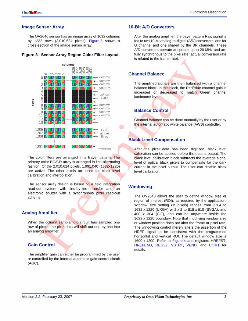
The OV2640 sensor has an image array of 1632 columnsby 1232 rows (2,010,624 pixels). Figure 3 shows across-section of the image sensor array.
Figure 3 Sensor Array Region Color Filter Layout
The color filters are arranged in a Bayer pattern. Theprimary color BG/GR array is arranged in line-alternatingfashion. Of the 2,010,624 pixels, 1,991,040 (1632x1220)are active. The other pixels are used for black levelcalibration and interpolation.
The sensor array design is based on a field integrationread-out system with line-by-line transfer and anelectronic shutter with a synchronous pixel read-outscheme.
Analog Amplifier
When the column sample/hold circuit has sampled onerow of pixels, the pixel data will shift out one-by-one intoan analog amplifier.
Gain Control
The amplifier gain can either be programmed by the useror controlled by the internal automatic gain control circuit(AGC).
B GG RB GG RB GG RB GG R
B GG RB GG RB GG RB GG R
B GG R
B GG R
B GG R
B GG R
B GG R
B GG R
B GG R
B GG R
B GG R
B GG R
B GG R
B GG R
B GG R
G R G R G R G R G R G R
B G B G B G
B GG R
B GG R
B GG R
B G B G B G
B GG RB GG RB GG R
B GG RB GG RB GG RB GG R
B GG RB GG RB GG RB GG R
B GG R
B GG R
B GG R
B GG R
B GG R
B GG R
B GG R
B GG R
B GG R
B GG R
B GG RB GG RB GG R
0 1 2 3 4 5 1626
1627
1628
1629
1630
1631
89
10111213
120612071208
1231
76543210
row
s
columns
dummydummydummydummy
dummydummydummydummy
opticalblack
1220activelines
2640CSP_DS_003
Version 2.2, February 23, 2007 P
10-Bit A/D Converters
After the analog amplifier, the bayer pattern Raw signal isfed to two 10-bit analog-to-digital (A/D) converters, one forG channel and one shared by the BR channels. TheseA/D converters operate at speeds up to 20 MHz and arefully synchronous to the pixel rate (actual conversion rateis related to the frame rate).
Channel Balance
The amplified signals are then balanced with a channelbalance block. In this block, the Red/Blue channel gain isincreased or decreased to match Green channelluminance level.
Balance Control
Channel Balance can be done manually by the user or bythe internal automatic white balance (AWB) controller.
Black Level Compensation
After the pixel data has been digitized, black levelcalibration can be applied before the data is output. Theblack level calibration block subtracts the average signallevel of optical black pixels to compensate for the darkcurrent in the pixel output. The user can disable blacklevel calibration.
Windowing
The OV2640 allows the user to define window size orregion of interest (ROI), as required by the application.Window size setting (in pixels) ranges from 2 x 4 to1632 x 1220 (UXGA) or 2 x 2 to 818 x 610 (SVGA), and408 x 304 (CIF), and can be anywhere inside the1632 x 1220 boundary. Note that modifying window sizeor window position does not alter the frame or pixel rate.The windowing control merely alters the assertion of theHREF signal to be consistent with the programmedhorizontal and vertical ROI. The default window size is1600 x 1200. Refer to Figure 4 and registers HREFST,HREFEND, REG32, VSTRT, VEND, and COM1 fordetails.
roprietary to OmniVision Technologies, Inc. 3

OV2640 Color CMOS UXGA (2.0 MegaPixel) OmniPixel2™ CAMERACHIP™ Sensor Omni ision
Figure 4 Windowing
Zooming and Panning Mode
The OV2640 provides zooming and panning modes. Theuser can select this mode under SVGA/CIF mode timing.The related zoom ratios will be 2:1 of UXGA for SVGA and4:1 of UXGA for CIF. Registers ZOOMS[7:0] (0x49) andCOM19[1:0] (0x48) define the vertical line start point.Register ARCOM2[2] (0x34) defines the horizontal startpoint.
Sub-sampling Mode
The OV2640 supports two sub-sampling modes. Eachsub-sampling mode has different resolution and maximumframe rate. These modes are described in the followingsections.
SVGA mode
The OV2640 can be programmed to output 800 x 600(SVGA) sized images for applications where higherresolution image capture is not required. In this mode,both horizontal and vertical pixels will be sub-sampledwith an aspect ratio of 4:2 as shown in Figure 5.
Figure 5 SVGA Sub-Sampling Mode
column start
row start
HR
EF
row end
column end
HREF
displaywindow
sensor array boundary
row
scolumns
2640CSP_DS_004
B GG RB GG R
B GG RB GG R
B GG R
B GG R
B GG R
B GG R
B GG R
B GG R
B GG R
B GG R
B GG R
B GG RB GG R
B GG R
B GG R
B GG RB GG R
B GG R
i i+1
i+2
i+3
i+4
i+5
i+6
i+7
i+8
i+9
n+4n+5n+6n+7
B skipped pixels
n+3n+2n+1
n
row
s
columns
2640CSP_DS_005
4 Proprietary to OmniVision Technologies, Inc.
CIF Mode
The OV2640 can also operate at a higher frame rate tooutput 400 x 296 sized images. Figure 6 shows thesub-sampling diagram in both horizontal and verticaldirections for CIF mode.
Figure 6 CIF Sub-Sampling Mode
Timing Generator and Control Logic
In general, the timing generator controls the following:• Frame Exposure Mode Timing• Frame Rate Adjust• Frame Rate Timing
Frame Exposure Mode Timing
The OV2640 supports frame exposure mode. Typically,the frame exposure mode must work with the aid of anexternal shutter.
The frame exposure pin, FREX (pin B2), is the frameexposure mode enable pin and the EXPST_B pin (pin A2)serves as the sensor's exposure start trigger. When theexternal master device asserts the FREX pin high, thesensor array is quickly pre-charged and stays in resetmode until the EXPST_B pin goes low (sensor exposuretime can be defined as the period between EXPST_B lowand shutter close). After the FREX pin is pulled low, thevideo data stream is then clocked to the output port in aline-by-line manner. After completing one frame of data
B GG RB GG R
B GG RB GG R
B GG R
B GG R
B GG R
B GG R
B GG R
B GG R
B GG R
B GG R
B GG R
B GG RB GG R
B GG R
B GG R
B GG R
B GG R
B GG R
B GG R
B GG R
B GG R
B GG R
B GG R
B GG R
B GG R
B GG R
B GG R
B GG R
B GG R
B GG R
B GG R
B GG R
B GG R
B GG R
B GG R
B GG R
B GG R
B GG R
B GG R
B GG R
B GG R
B GG R
B GG R
B GG R
B GG R
B GG R
B GG R
B GG R
B GG R
B GG R
B GG R
B GG R
B GG R
B GG R
B GG R
B GG R
B GG R
B GG R
B GG R
B GG R
B GG R
B GG R
B GG R
B GG R
B GG R
B GG R
B GG R
B GG R
B GG R
B GG R
B GG R
B GG R
B GG R
B GG R
B GG R
B GG R
B GG R
B GG R
B GG R
B GG R
B GG R
B GG R
B GG R
B GG R
B GG R
B GG R
B GG R
B GG R
B GG R
B GG R
B GG R
B GG R
B GG R
B GG R
B GG R
B GG R
B GG R
B GG R
B GG R
B GG R
B GG R
B GG R
B GG R
B GG R
B GG R
B GG R
B GG R
B GG R
B GG R
B GG R
B GG R
B GG R
B GG R
B GG R
B GG R
B GG R
B GG R
B GG R
B GG R
B GG R
B GG R
B GG R
B GG R
B GG R
B GG R
B GG R
B GG R
B GG R
B GG R
B GG R
B GG R
B GG R
B GG R
B GG R
B GG R
B GG R
B GG R
B GG R
B GG R
B GG RB GG R
B GG R
i i+1
i+2
i+3
i+4
i+5
i+6
i+7
i+8
i+9
i+10
i+11
i+12
i+13
i+14
i+15
i+16
i+17
i+18
i+19
i+20
i+21
i+22
i+23
n+4n+5n+6n+7n+8n+9
n+10n+11n+12n+13n+14n+15n+16n+17n+18n+19n+20n+21n+22n+23
B skipped pixels
n+3n+2n+1
n
row
s
columns
2640CSP_DS_006
Version 2.2, February 23, 2007

Functional DescriptionOmni ision
output, the OV2640 will output continuous live video dataunless in single frame transfer mode. Figure 16 andFigure 17 show the detailed timing and Table 11 showsthe timing specifications for this mode.
Frame Rate Adjust
The OV2640 offers three methods for frame rateadjustment:• Clock prescaler: (see “CLKRC” on page 22)
By changing the system clock divide ratio and PLL, the frame rate and pixel rate will change together. This method can be used for dividing the frame/pixel rate by: 1/2, 1/3, 1/4 … 1/64 of the input clock rate.
• Line adjustment: (see “REG2A” on page 24 and “FRARL” on page 24)By adding a dummy pixel timing in each line (between HREF and pixel data out), the frame rate can be changed while leaving the pixel rate as is.
• Vertical sync adjustment: By adding dummy line periods to the vertical sync period (see “ADDVSL” on page 24 and “ADDVSH” on page 25 or see “FLL” on page 25 and “FLH” on page 25), the frame rate can be altered while the pixel rate remains the same.
Frame Rate Timing
Default frame timing is illustrated in Figure 13, Figure 14,and Figure 15. Refer to Table 1 for the actual pixel rate atdifferent frame rates.
Digital Signal Processor (DSP)
This block controls the interpolation from Raw data toRGB and some image quality control.• Edge enhancement (a two-dimensional high pass
filter)• Color space converter (can change Raw data to RGB
or YUV/YCbCr)• RGB matrix to eliminate color cross talk• Hue and saturation control• Programmable gamma control• Transfer 10-bit data to 8-bit• White pixel canceling• De-noise
Table 1 Frame/Pixel Rates in UXGA Mode
Frame Rate (fps) 15 7.5 2.5 1.25
PCLK (MHz) 36 18 6 3
Version 2.2, February 23, 2007 P
Output Formatter
This block controls all output and data formatting requiredprior to sending the image out.
Scaling Image Output
The OV2640 is capable of scaling down the image sizefrom CIF to 40x30. By using SCCB registers, the user canoutput the desired image size. At certain image sizes,HREF is not consistent in a frame.
Compression Engine
As shown in Figure 7, the Compression Engine consistsof three major blocks:• DCT• QZ• Entropy Encoder
Figure 7 Compression Engine Block Diagram
Microcontroller
The OV2640 embeds an 8-bit microcontroller with512-byte data memory and 4 KB program memory. Itprovides the flexibility of decoding protocol commandsfrom the host for controlling the system, as well as theability to fine tune image quality.
SCCB Interface
The Serial Camera Control Bus (SCCB) interface controlsthe CAMERACHIP sensor operation. Refer to OmniVisionTechnologies Serial Camera Control Bus (SCCB)Specification for detailed usage of the serial control port.
Strobe Mode
The OV2640 has a Strobe mode that allows it to work withan external flash and LED.
videodata
compressedstream
compression engine
scalefactor
entropy encoderQZDCT
Q-table H-table marker
2640CSP_DS_007
roprietary to OmniVision Technologies, Inc. 5

OV2640 Color CMOS UXGA (2.0 MegaPixel) OmniPixel2™ CAMERACHIP™ Sensor Omni ision
ResetThe OV2640 includes a RESETB pin (pin C6) that forcesa complete hardware reset when it is pulled low (GND).The OV2640 clears all registers and resets them to theirdefault values when a hardware reset occurs. A reset canalso be initiated through the SCCB interface.
Power Down ModeTwo methods are available to place the OV2640 intopower-down mode: hardware power-down and SCCBsoftware power-down.
To initiate hardware power-down, the PWDN pin (pin B6)must be tied to high. When this occurs, the OV2640internal device clock is halted and all internal counters arereset.
Executing a software power-down through the SCCBinterface suspends internal circuit activity but does nothalt the device clock. All register content is maintained instandby mode.
Digital Video Port
MSB/LSB SwapThe OV2640 has a 10-bit digital video port. The MSB andLSB can be swapped with the control registers. Figure 8shows some examples of connections with externaldevices.
Figure 8 Connection Examples
Y9Y8Y7Y6Y5Y4Y3Y2Y1Y0
Y8
OV2640 externaldevice
MSB Y9
Y7Y6Y5Y4Y3Y2Y1
LSB Y0
Y0Y1Y2Y3Y4Y5Y6Y7Y8Y9
Y8
OV2640 externaldevice
LSB Y9
Y7Y6Y5Y4Y3Y2Y1
MSB Y0
default 10-bit connection swap 10-bit connection
Y7Y6Y5Y4Y3Y2Y1Y0
Y8
OV2640 externaldevice
MSB Y9
Y7Y6Y5Y4Y3Y2Y1
LSB Y0
Y0Y1Y2Y3Y4Y5Y6Y7
Y8
OV2640 externaldevice
LSB Y9
Y7Y6Y5Y4Y3Y2Y1
MSB Y0
default 8-bit connection swap 8-bit connection2640CSP_DS_010
6 Proprietary to OmniVision Technologies, Inc.
Line/Pixel TimingThe OV2640 digital video port can be programmed towork in either master or slave mode.
In both master and slave modes, pixel data output issynchronous with PCLK (or MCLK if port is a slave),HREF, and VSYNC. The default PCLK edge for valid datais the negative edge but may be programmed usingregister COM10[4] for the positive edge. Basic line/pixeloutput timing and pixel timing specifications are shown inFigure 12 and Table 10.
Also, using register COM10[5], PCLK output can be gatedby the active video period defined by the HREF signal.See Figure 9 for details.
Figure 9 PCLK Output Only at Valid Pixels
The specifications shown in Table 10 apply forDVDD = +1.2 V, DOVDD = +2.8 V, TA = 25°C, sensorworking at 15 fps, external loading = 20 pF.
Pixel Output Pattern
Table 2 shows the output data order from the OV2640.The data output sequence following the first HREF andafter VSYNC is: B0,0 G0,1 B0,2 G0,3… B0,1598 G0,1599.After the second HREF the output is G1,0 R1,1 G1,2 R1,3…G1,1598 R1,1599…, etc. If the OV2640 is programmed tooutput SVGA resolution data, horizontal and verticalsub-sampling will occur. The default output sequence forthe first line of output will be: B0,0 G0,1 B0,4 G0,5… B0,1596G0,1597. The second line of output will be: G1,0 R1,1 G1,4R1,5… G1,1596 R1,1597.
Table 2 Data Pattern
R/C 0 1 2 3 . . . 1598 1599
0 B0,0 G0,1 B0,2 G0,3 . . . B0,1598 G0,1599
1 G1,0 R1,1 G1,2 R1,3 . . . G1,1598 R1,1599
2 B2,0 G2,1 B2,2 G2,3 . . . B2,1598 G2,1599
3 G3,0 R3,1 G3,2 R3,3 . . . G3,1598 R3,1599
.
...
1198 B1198,0 G1198,1 B1198,2 G1198,3 . . . B1198,1598 G1198,1599
1199 G1199,0 R1199,1 G1199,2 R1199,3 . . . G1199,1598 R1199,1599
PCLKPCLK active edge negative
PCLK active edge positive
HREF
PCLK
VSYNC2640CSP_DS_011
Version 2.2, February 23, 2007
Pin DescriptionOmni ision
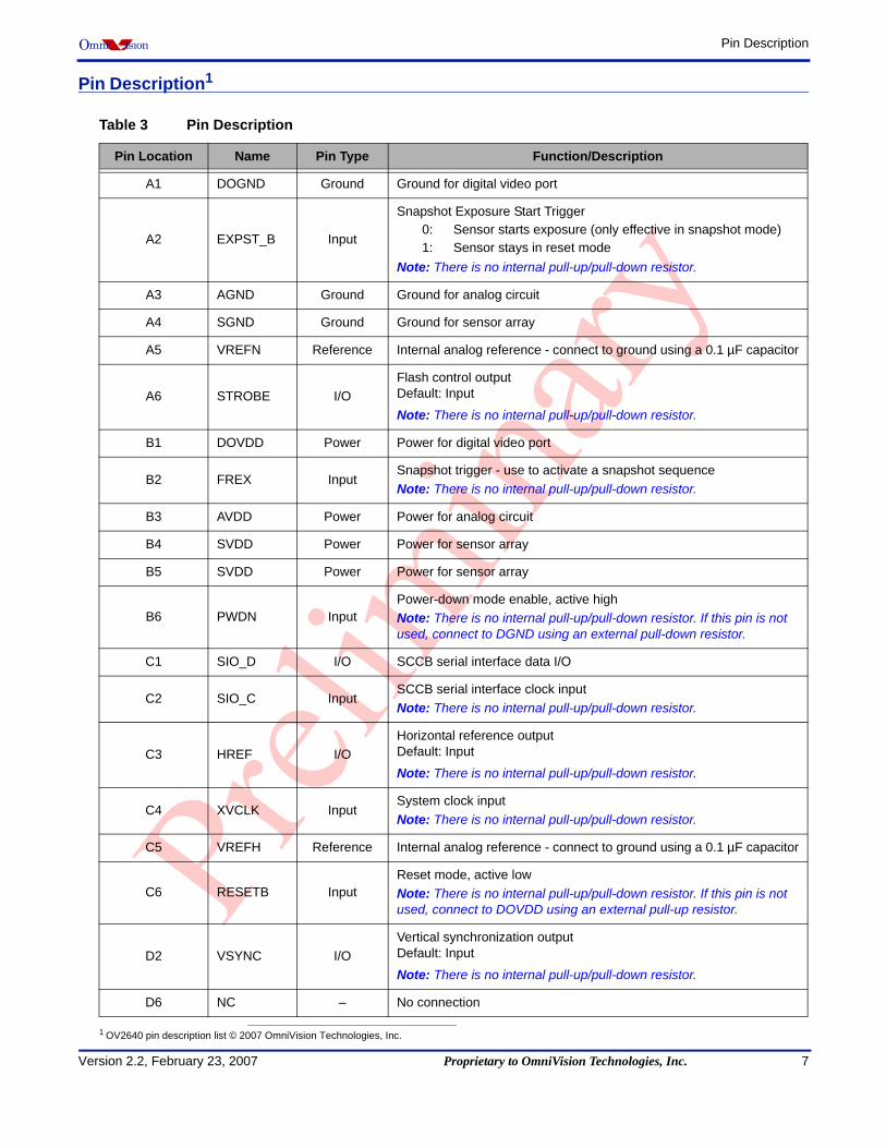
Pin Description1
1 OV2640 pin description list © 2007 OmniVision Technologies, Inc.
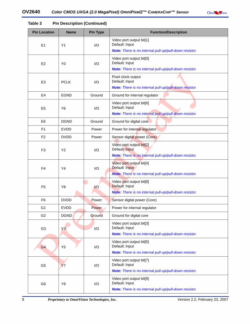
Table 3 Pin Description
Pin Location Name Pin Type Function/Description
A1 DOGND Ground Ground for digital video port
A2 EXPST_B Input
Snapshot Exposure Start Trigger0: Sensor starts exposure (only effective in snapshot mode)1: Sensor stays in reset mode
Note: There is no internal pull-up/pull-down resistor.
A3 AGND Ground Ground for analog circuit
A4 SGND Ground Ground for sensor array
A5 VREFN Reference Internal analog reference - connect to ground using a 0.1 µF capacitor
A6 STROBE I/OFlash control outputDefault: Input
Note: There is no internal pull-up/pull-down resistor.
B1 DOVDD Power Power for digital video port
B2 FREX InputSnapshot trigger - use to activate a snapshot sequenceNote: There is no internal pull-up/pull-down resistor.
B3 AVDD Power Power for analog circuit
B4 SVDD Power Power for sensor array
B5 SVDD Power Power for sensor array
B6 PWDN InputPower-down mode enable, active highNote: There is no internal pull-up/pull-down resistor. If this pin is not used, connect to DGND using an external pull-down resistor.
C1 SIO_D I/O SCCB serial interface data I/O
C2 SIO_C InputSCCB serial interface clock inputNote: There is no internal pull-up/pull-down resistor.
C3 HREF I/OHorizontal reference outputDefault: Input
Note: There is no internal pull-up/pull-down resistor.
C4 XVCLK InputSystem clock inputNote: There is no internal pull-up/pull-down resistor.
C5 VREFH Reference Internal analog reference - connect to ground using a 0.1 µF capacitor
C6 RESETB InputReset mode, active lowNote: There is no internal pull-up/pull-down resistor. If this pin is not used, connect to DOVDD using an external pull-up resistor.
D2 VSYNC I/OVertical synchronization outputDefault: Input
Note: There is no internal pull-up/pull-down resistor.
D6 NC – No connection
Version 2.2, February 23, 2007 Proprietary to OmniVision Technologies, Inc. 7
OV2640 Color CMOS UXGA (2.0 MegaPixel) OmniPixel2™ CAMERACHIP™ Sensor Omni ision
E1 Y1 I/OVideo port output bit[1]Default: Input
Note: There is no internal pull-up/pull-down resistor.
E2 Y0 I/OVideo port output bit[0]Default: Input
Note: There is no internal pull-up/pull-down resistor.
E3 PCLK I/OPixel clock outputDefault: Input
Note: There is no internal pull-up/pull-down resistor.
E4 EGND Ground Ground for internal regulator
E5 Y6 I/OVideo port output bit[6]Default: Input
Note: There is no internal pull-up/pull-down resistor.
E6 DGND Ground Ground for digital core
F1 EVDD Power Power for internal regulator
F2 DVDD Power Sensor digital power (Core)
F3 Y2 I/OVideo port output bit[2]Default: Input
Note: There is no internal pull-up/pull-down resistor.
F4 Y4 I/OVideo port output bit[4]Default: Input
Note: There is no internal pull-up/pull-down resistor.
F5 Y8 I/OVideo port output bit[8]Default: Input
Note: There is no internal pull-up/pull-down resistor.
F6 DVDD Power Sensor digital power (Core)
G1 EVDD Power Power for internal regulator
G2 DGND Ground Ground for digital core
G3 Y3 I/OVideo port output bit[3]Default: Input
Note: There is no internal pull-up/pull-down resistor.
G4 Y5 I/OVideo port output bit[5]Default: Input
Note: There is no internal pull-up/pull-down resistor.
G5 Y7 I/OVideo port output bit[7]Default: Input
Note: There is no internal pull-up/pull-down resistor.
G6 Y9 I/OVideo port output bit[9]Default: Input
Note: There is no internal pull-up/pull-down resistor.
Table 3 Pin Description (Continued)
Pin Location Name Pin Type Function/Description
8 Proprietary to OmniVision Technologies, Inc. Version 2.2, February 23, 2007

Pin DescriptionOmni ision
Figure 10 Pinout Diagram1
1 OV2640 pin diagram © 2007 OmniVision Technologies, Inc.
Table 4 Ball Matrix
1 2 3 4 5 6
A DOGND EXPST_B AGND SGND VREFN STROBE
B DOVDD FREX AVDD SVDD SVDD PWDN
C SIO_D SIO_C HREF XVCLK VREFN RESETB
D VSYNC NC
E Y1 Y0 PCLK EGND Y6 DGND
F EVDD DVDD Y2 Y4 Y8 DVDD
G EVDD DGND Y3 75 Y7 Y9
A1
DOGND
A2
EXPST_B
A3
AGND
OV2640
A4
SGND
A5
VREFN
B1
DOVDD
B2
FREX
B4
SVDD
B3
AVDD
B5
SVDD
C1
SIO_D
C2
SIO_C
C4
XVCLK
C5
VREFH
D2
VSYNC
C3
HREF
E1
Y1
E2
Y0
E4
EGND
E3
PCLK
E5
Y6
F1
EVDD
F2
DVDD
F3
Y2
F4
Y4
F5
Y8
A6
STROBE
B6
PWDN
C6
RESETB
D6
NC
E6
DGND
F6
DVDD
G1
EVDD
G2
DGND
G3
Y3
G4
Y5
G5
Y7
G6
Y9
2640CSP_DS_010
Version 2.2, February 23, 2007 Proprietary to OmniVision Technologies, Inc. 9

OV2640 Color CMOS UXGA (2.0 MegaPixel) OmniPixel2™ CAMERACHIP™ Sensor Omni ision
Electrical Characteristics
NOTE: Exceeding the Absolute Maximum ratings shown above invalidates all AC and DC electrical specifications and mayresult in permanent device damage.
Table 5 Absolute Maximum Ratings
Ambient Storage Temperature -40ºC to +95ºC
Supply Voltages (with respect to Ground)
VDD-A 4.5V
VDD-C 3V
VDD-IO 4.5V
All Input/Output Voltages (with respect to Ground) -0.3V to VDD-IO+1V
Lead-free Temperature, Surface-mount process 245ºC
Table 6 DC Characteristics (-30°C < TA < 70°C)
Symbol Parameter Min Typ Max Unit
Supply
VDD-A Supply voltage 2.5a
a. If using internal regulator for DVDD, VDD-A requires greater than or equal to 2.65V
2.8 3.0 V
VDD-D Supply voltage 1.24 1.3 1.36 V
VDD-IO Supply voltageb
b. 1.8V I/O is supported. Contact your local OmniVision FAE for further details.
1.71 2.8 3.3 V
IDDA-A Active (operating) currentc
c. At 25ºC, VDD-A = 2.8V, VDD-D = 1.3V, and VDD-IO = 1.8V for 15 fps in UXGA mode
30 40 mA
IDDA-D Active (operating) currentc 30 (YUV)45 (Compressed)
40 (YUV)60 (Compressed) mA
IDDA-IO Active (operating) currentc 6 15 mA
IDDS-SCCBStandby currentd
d. IDDS-SCCB refers to SCCB-initiated Standby, while IDDS-PWDN refers to PWDN pad-initiated Standby
1 2 mA
IDDS-PWDN 900 2000 µA
Digital Inputs
VIL Input voltage LOW 0.54 V
VIH Input voltage HIGH 1.26 V
CIN Input capacitor 10 pF
Digital Outputs (standard loading 25 pF)
VOH Output voltage HIGH 1.62 V
VOL Output voltage LOW 0.18 V
Serial Interface Inputs
VIL SIO_C and SIO_D -0.5 0 0.54 V
VIH SIO_C and SIO_D 1.26 1.8 2.3 V
10 Proprietary to OmniVision Technologies, Inc. Version 2.2, February 23, 2007

Electrical CharacteristicsOmni ision
Table 7 AC Characteristics (TA = 25°C, VDD-A = 2.8V)
Symbol Parameter Min Typ Max Unit
ADC Parameters
B Analog bandwidth 20 MHz
DLE DC differential linearity error 0.5 LSB
ILE DC integral linearity error 1 LSB
Settling time for hardware reset <1 ms
Settling time for software reset <1 ms
Settling time for UXGA/SVGA mode change <1 ms
Settling time for register setting <300 ms
Table 8 Timing Characteristics
Symbol Parameter Min Typ Max Unit
Oscillator and Clock Input
fOSC Frequency (XVCLK) 6 24 MHz
tr, tf Clock input rise/fall time 5 ns
Clock input duty cycle 45 50 55 %
Version 2.2, February 23, 2007 Proprietary to OmniVision Technologies, Inc. 11
OV2640 Color CMOS UXGA (2.0 MegaPixel) OmniPixel2™ CAMERACHIP™ Sensor Omni ision
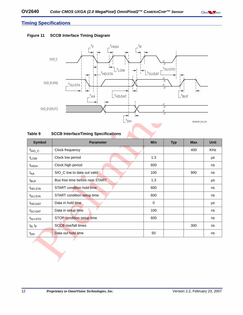
Timing Specifications
Figure 11 SCCB Interface Timing Diagram
Table 9 SCCB InterfaceTiming Specifications
Symbol Parameter Min Typ Max Unit
fSIO_C Clock frequency 400 KHz
tLOW Clock low period 1.3 µs
tHIGH Clock high period 600 ns
tAA SIO_C low to data out valid 100 900 ns
tBUF Bus free time before new START 1.3 µs
tHD:STA START condition hold time 600 ns
tSU:STA START condition setup time 600 ns
tHD:DAT Data in hold time 0 µs
tSU:DAT Data in setup time 100 ns
tSU:STO STOP condition setup time 600 ns
tR, tF SCCB rise/fall times 300 ns
tDH Data out hold time 50 ns
SIO_D (OUT)
tAA
tDH
SIO_C
tF tRtHIGH
tLOW tSU:DAT
SIO_D (IN)
tHD:DAT
tSU:STO
tSU:STA
tHD:STA
tBUF
2640CSP_DS_011
12 Proprietary to OmniVision Technologies, Inc. Version 2.2, February 23, 2007

Timing SpecificationsOmni ision
Figure 12 UXGA, SVGA, and CIF Line/Pixel Output Timing
Table 10 Pixel Timing Specifications
Symbol Parameter Min Typ Max Unit
tp PCLK perioda
a. PCLK running at 36MHz, CL = 20pF, and DOVDD = 1.8V
27.78 ns
tpr PCLK rising timea 1.2 2.2 3.2 ns
tpf PCLK falling timea 0.8 1.6 2.4 ns
tdphr PCLK negative edge to HREF rising edge 0 5 ns
tdphf PCLK negative edge to HREF negative edge 0 5 ns
tdpd PCLK negative edge to data output delay 0 5 ns
tsu Data bus setup time 15 ns
thd Data bus hold time 8 ns
Y[9:0]
HREF
P1599/799/399 P1598/798/398 P1599/799/399invalid
data P0 P1 P2
PCLK orMCLK
tsu
thd
tp tpr
tdphr tdphf
tdpd
tpf
2640CSP_DS_012
Version 2.2, February 23, 2007 Proprietary to OmniVision Technologies, Inc. 13
OV2640 Color CMOS UXGA (2.0 MegaPixel) OmniPixel2™ CAMERACHIP™ Sensor Omni ision
Figure 13 UXGA Frame Timing
Figure 14 SVGA Frame Timing
Figure 15 CIF Mode Frame Timing
Y[9:0]
HREF
VSYNC
1248 x tLINE
4 x tLINE 27193 tP
322 tP
P0 - P1599
1600 tP
row 0
invalid data
row 1 row 2 row 1199
tLINE = 1922 tP 57697 tP
2640CSP_DS_013
Y[9:0]
HREF
VSYNC
672 x tLINE
4 x tLINE 7415 tP
390 tP
P0 - P799
800 tP
row 0
invalid data
row 1 row 2 row 599
tLINE = 1190 tP 73895 tP
2640CSP_DS_014
Y[9:0]
HREF
VSYNC
336 x tLINE
4 x tLINE 3707.5 tP
195 tP
P0 - P399
400 tP
row 0
invalid data
row 1 row 2 row 295
tLINE = 595 tP 17907.5 tP
2640CSP_DS_015
14 Proprietary to OmniVision Technologies, Inc. Version 2.2, February 23, 2007

Timing SpecificationsOmni ision
Figure 16 Frame Exposure Mode Timing with EXPST_B Staying Low
Figure 17 Frame Exposure Mode Timing with EXPST_B Asserted
NOTE 1) FREX must stay high long enough to ensure the entire sensor has been reset.2) Shutter must be closed no later then 3896 tp after VSYNC falling edge.
Table 11 Frame Exposure Timing Specifications
Symbol Min Typ Max Unit
tline 1922 (UXGA) tp
tvs 4 tline
tdfvr 8 9 tp
tdhv 38964 (UXGA) tp
tdhso 0 ns
tdef 20 tp
tdes 8 1900 (UXGA) tp
shutter
FREX
sensortiming
VSYNC
HREF
Y[9:0]
row X row 0 row 1 row 1199
tdhv 4 x tLINE4 x tLINE
tLINE exposure time
"flash turn on"
shutter open
tdfvr
no following live video frame ifset to transfer single frame
sensorprecharge
2640CSP_DS_016
shutter
FREX
EXPST_B
sensortiming
VSYNC
HREF
Y[9:0]
row X row 0 row 1 row 1199
tdef
tdhv 4 x tLINE4 x tLINE
tpre exposure time
"flash turn on"
shutter open
tdes
tdfvr
no following live video frame ifset to transfer single frame
sensorprecharge
2640CSP_DS_017
Version 2.2, February 23, 2007 Proprietary to OmniVision Technologies, Inc. 15

OV2640 Color CMOS UXGA (2.0 MegaPixel) OmniPixel2™ CAMERACHIP™ Sensor Omni ision
OV2640 Light Response
Figure 18 OV2640 Light Response
wavelength (nm)
sens
itiv
ity
300
380
420
460
500
540
580
620
660
700
740
780
820
860
900
940
980
1020
1060
1100
1180
1220
0
20
40
60
80
100
120
140
160
180
200RGB
2640CSP_DS_018
16 Proprietary to OmniVision Technologies, Inc. Version 2.2, February 23, 2007

Register SetOmni ision
Register Set
Table 12 and Table 13 provides a list and description of the Device Control registers contained in the OV2640. For all registerEnable/Disable bits, ENABLE = 1 and DISABLE = 0. The device slave addresses are 60 for write and 61 for read.
There are two different sets of register banks. Register 0xFF controls which set is accessible. When register 0xFF=00,Table 12 is effective. When register 0xFF=01, Table 13 is effective.
Table 12 Device Control Register List (when 0xFF = 00) (Sheet 1 of 4)
Address(Hex)
RegisterName
Default(Hex) R/W Description
00-04 RSVD XX – Reserved
05 R_BYPASS 0x1 RW
Bypass DSPBit[7:1]: ReservedBit[0]: Bypass DSP select
0: DSP1: Bypass DSP, sensor out directly
06-43 RSVD XX – Reserved
44 Qs 0C RW Quantization Scale Factor
45-4F RSVD XX – Reserved
50 CTRLl[7:0] 00 RW
Bit[7]: LP_DPBit[6]: RoundBit[5:3]: V_DIVIDERBit[2:0]: H_DIVIDER
51 HSIZE[7:0] 40 RW H_SIZE[7:0] (real/4)
52 VSIZE[7:0] F0 RW V_SIZE[7:0] (real/4)
53 XOFFL[7:0] 00 RW OFFSET_X[7:0]
54 YOFFL[7:0] 00 RW OFFSET_Y[7:0]
55 VHYX[7:0] 08 RW
Bit[7]: V_SIZE[8]Bit[6:4]: OFFSET_Y[10:8]Bit[3]: H_SIZE[8]Bit[2:0]: OFFSET_X[10:8]
56 DPRP[7:0] 00 RWBit[7:4]: DP_SELYBit[3:0]: DP_SELX
57 TEST[3:0] 00 RWBit[7]: H_SIZE[9]Bit[6:0]: Reserved
5A ZMOW[7:0] 58 RW OUTW[7:0] (real/4)
5B ZMOH[7:0] 48 RW OUTH[7:0] (real/4)
5C ZMHH[1:0] 00 RWBit[7:4]: ZMSPD (zoom speed)Bit[2]: OUTH[8]Bit[1:0]: OUTW[9:8]
5D-7B RSVD XX – Reserved
7C BPADDR[3:0] 00 RW SDE Indirect Register Access: Address
Version 2.2, February 23, 2007 Proprietary to OmniVision Technologies, Inc. 17
OV2640 Color CMOS UXGA (2.0 MegaPixel) OmniPixel2™ CAMERACHIP™ Sensor Omni ision
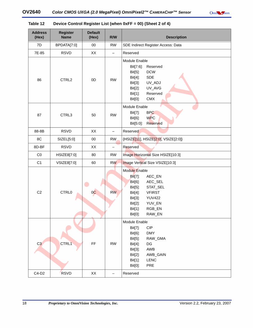
7D BPDATA[7:0] 00 RW SDE Indirect Register Access: Data
7E-85 RSVD XX – Reserved
86 CTRL2 0D RW
Module EnableBit[7:6]: ReservedBit[5]: DCWBit[4]: SDEBit[3]: UV_ADJBit[2]: UV_AVGBit[1]: ReservedBit[0]: CMX
87 CTRL3 50 RW
Module EnableBit[7]: BPCBit[6]: WPCBit[5:0]: Reserved
88-8B RSVD XX – Reserved
8C SIZEL[5:0] 00 RW HSIZE[11], HSIZE[2:0], VSIZE[2:0]
8D-BF RSVD XX – Reserved
C0 HSIZE8[7:0] 80 RW Image Horizontal Size HSIZE[10:3]
C1 VSIZE8[7:0] 60 RW Image Vertical Size VSIZE[10:3]
C2 CTRL0 0C RW
Module EnableBit[7]: AEC_ENBit[6]: AEC_SELBit[5]: STAT_SELBit[4]: VFIRSTBit[3]: YUV422Bit[2]: YUV_ENBit[1]: RGB_ENBit[0]: RAW_EN
C3 CTRL1 FF RW
Module EnableBit[7]: CIPBit[6]: DMYBit[5]: RAW_GMABit[4]: DGBit[3]: AWBBit[2]: AWB_GAINBit[1]: LENCBit[0]: PRE
C4-D2 RSVD XX – Reserved
Table 12 Device Control Register List (when 0xFF = 00) (Sheet 2 of 4)
Address(Hex)
RegisterName
Default(Hex) R/W Description
18 Proprietary to OmniVision Technologies, Inc. Version 2.2, February 23, 2007

Register SetOmni ision
D3 R_DVP_SP 82 RW
Bit[7]: Auto modeBit[6:0]: DVP output speed control
DVP PCLK = sysclk (48)/[6:0] (YUV0); = sysclk (48)/(2*[6:0]) (RAW)
D4-D9 RSVD XX – Reserved
DA IMAGE_MODE 00 RW
Image Output Format SelectBit[7]: ReservedBit[6]: Y8 enable for DVPBit[5]: ReservedBit[4]: JPEG output enable
0: Non-compressed1: JPEG output
Bit[3:2]: DVP output format00: YUV42201: RAW10 (DVP)10: RGB56511: Reserved
Bit[1]: HREF timing select in DVP JPEG output mode0: HREF is same as sensor1: HREF = VSYNC
Bit[0]: Byte swap enable for DVP0: High byte first YUYV (C2[4]=0)
YVYU (C2[4] = 1) 1: Low byte first UYVY (C2[4] =0)
VYUY (C2[4] =1)
DB-DF RSVD XX – Reserved
E0 RESET 04 RW
ResetBit[7]: ReservedBit[6]: MicrocontrollerBit[5]: SCCBBit[4]: JPEGBit[3]: ReservedBit[2]: DVPBit[1]: IPUBit[0]: CIF
E1-EC RSVD XX – Reserved
ED REGED 1F RW
Register EDBit[7:5]: ReservedBit[4]: Clock output power-down pin status
0: Data output pin hold at last state before power-down
1: Tri-state data output pin upon power-downBit[3:0]: Reserved
EE-EF RSVD XX – Reserved
F0 MS_SP 04 RW SCCB Master Speed
Table 12 Device Control Register List (when 0xFF = 00) (Sheet 3 of 4)
Address(Hex)
RegisterName
Default(Hex) R/W Description
Version 2.2, February 23, 2007 Proprietary to OmniVision Technologies, Inc. 19

OV2640 Color CMOS UXGA (2.0 MegaPixel) OmniPixel2™ CAMERACHIP™ Sensor Omni ision
F1-F6 RSVD XX – Reserved
F7 SS_ID 60 RW SCCB Slave ID
F8 SS_CTRL 01 RW
SCCB Slave ControlBit[7:6]: ReservedBit[5]: Address auto-increase enableBit[4]: ReservedBit[3]: SCCB enableBit[2]: Delay SCCB master clockBit[1]: Enable SCCB master accessBit[0]: Enable sensor pass through access
F9 MC_BIST 40 RW
Bit[7]: Microcontroller ResetBit[6]: Boot ROM selectBit[5]: R/W 1 error for 12K-byte memoryBit[4]: R/W 0 error for 12K-byte memoryBit[3]: R/W 1 error for 512-byte memoryBit[2]: R/W 0 error for 512-byte memoryBit[1]: BIST busy bit for read; One-shot reset of
microcontroller for writeBit[0]: Launch BIST
FA MC_AL 00 RW Program Memory Pointer Address Low Byte
FB MC_AH 00 RW Program Memory Pointer Address High Byte
FC MC_D 80 RWProgram Memory Pointer Access AddressBoundary of register address to separate DSP and sensor register
FD P_CMD 00 RW SCCB Protocol Command Register
FE P_STATUS 00 RW SCCB Protocol Status Register
FF RA_DLMT 7F RW
Register Bank SelectBit[7:1]: ReservedBit[0]: Register bank select
0: DSP address1: Sensor address
NOTE: All other registers are factory-reserved. Please contact OmniVision Technologies for reference register settings.
Table 12 Device Control Register List (when 0xFF = 00) (Sheet 4 of 4)
Address(Hex)
RegisterName
Default(Hex) R/W Description
20 Proprietary to OmniVision Technologies, Inc. Version 2.2, February 23, 2007

Register SetOmni ision
Table 13 Device Control Register List (when 0xFF = 01) (Sheet 1 of 6)
Address(Hex)
RegisterName
Default(Hex) R/W Description
00 GAIN 00 RW
AGC Gain Control LSBsBit[7:0]: Gain setting
• Range: 1x to 32xGain = (Bit[7]+1) x (Bit[6]+1) x (Bit[5]+1) x (Bit[4]+1) x (1+Bit[3:0]/16)Note: Set COM8[2] = 0 to disable AGC.
01-02 RSVD XX – Reserved
03 COM10F (UXGA)0A (SVGA),06 (CIF)
RW
Common Control 1Bit[7:6]: Dummy frame control
00: Reserved01: Allow 1 dummy frame10: Allow 3 dummy frames11: Allow 7 dummy frames
Bit[5:4]: ReservedBit[3:2]: Vertical window end line control 2 LSBs
(8 MSBs in VEND[7:0] (0x1A))Bit[1:0]: Vertical window start line control 2 LSBs
(8 MSBs in VSTRT[7:0] (0x19))
04 REG04 20 RW
Register 04Bit[7]: Horizontal mirrorBit[6]: Vertical flipBit[4]: VREF bit[0]Bit[3]: HREF bit[0]Bit[2]: ReservedBit[1:0]: AEC[1:0]
(AEC[15:10] is in register REG45[5:0] (0x45),AEC[9:2] is in register AEC[7:0] (0x10))
05-07 RSVD XX – Reserved
08 REG08 40 RW Frame Exposure One-pin Control Pre-charge Row Number
09 COM2 00 RW
Common Control 2Bit[7:5]: ReservedBit[4]: Standby mode enable
0: Normal mode1: Standby mode
Bit[3]: ReservedBit[2]: Pin PWDN/RESETB used as SLVS/SLHSBit[1:0]: Output drive select
00: 1x capability01: 3x capability10: 2x capability11: 4x capability
0A PIDH 26 R Product ID Number MSB (Read only)
0B PIDL 41 R Product ID Number LSB (Read only)
Version 2.2, February 23, 2007 Proprietary to OmniVision Technologies, Inc. 21

OV2640 Color CMOS UXGA (2.0 MegaPixel) OmniPixel2™ CAMERACHIP™ Sensor Omni ision
0C COM3 38 RW
Common Control 3Bit[7:3]: ReservedBit[2]: Set banding manually
0: 60 Hz1: 50 Hz
Bit[1]: Auto set bandingBit[0]: Snapshot option
0: Enable live video output after snapshot sequence1: Output single frame only
0D-0F RSVD XX – Reserved
10 AEC 33 RW
Automatic Exposure Control 8 bits for AEC[9:2] (AEC[15:10] is in register REG45[5:0] (0x45), AEC[1:0] is in register REG04[1:0] (0x04))
AEC[15:0]: Exposure time
TEX = tLINE x AEC[15:0]
Note: The maximum exposure time is 1 frame period even if TEX is longer than 1 frame period.
11 CLKRC 00 RW
Clock Rate ControlBit[7]: Internal frequency doublers ON/OFF selection
0: OFF1: ON
Bit[6]: ReservedBit[5:0]: Clock divider
CLK = XVCLK/(decimal value of CLKRC[5:0] + 1)
12 COM7 00 RW
Common Control 7Bit[7]: SRST
1: Initiates system reset. All registers are set to factory default values after which the chip resumes normal operation
Bit[6:4]: Resolution selection000: UXGA (full size) mode010: CIF mode100: SVGA mode
Bit[3]: ReservedBit[2]: Zoom modeBit[1]: Color bar test pattern
0: OFF1: ON
Bit[0]: Reserved
Table 13 Device Control Register List (when 0xFF = 01) (Sheet 2 of 6)
Address(Hex)
RegisterName
Default(Hex) R/W Description
22 Proprietary to OmniVision Technologies, Inc. Version 2.2, February 23, 2007

Register SetOmni ision
13 COM8 C7 RW
Common Control 8Bit[7:6]: ReservedBit[5]: Banding filter selection
0: OFF1: ON, set minimum exposure time to 1/120s
Bit[4:3]: ReservedBit[2]: AGC auto/manual control selection
0: Manual1: Auto
Bit[1]: ReservedBit[0]: Exposure control
0: Manual1: Auto
14 COM9 50 RW
Common Control 9Bit[7:5]: AGC gain ceiling, GH[2:0]
000: 2x001: 4x010: 8x011: 16x100: 32x101: 64x11x: 128x
Bit[4:0]: Reserved
15 COM10 00 RW
Common Control 10 (if Bypass DSP is selected)Bit[7:6]: ReservedBit[5]: PCLK output selection
0: PCLK always output1: PCLK output qualified by HREF
Bit[4]: PCLK edge selection0: Data is updated at the falling edge of PCLK (user
can latch data at the next rising edge of PCLK)1: Data is updated at the rising edge of PCLK (user can
latch data at the next falling edge of PCLK)Bit[3]: HREF output polarity
0: Output positive HREF1: Output negative HREF, HREF negative for data
validBit[2]: ReservedBit[1]: VSYNC polarity
0: Positive1: Negative
Bit[0]: Reserved
16 RSVD XX – Reserved
17 HREFST 11 RWHorizontal Window Start MSB 8 bits (3 LSBs in REG32[2:0] (0x32))
Bit[10:0]: Selects the start of the horizontal window, each LSB represents two pixels
Table 13 Device Control Register List (when 0xFF = 01) (Sheet 3 of 6)
Address(Hex)
RegisterName
Default(Hex) R/W Description
Version 2.2, February 23, 2007 Proprietary to OmniVision Technologies, Inc. 23

OV2640 Color CMOS UXGA (2.0 MegaPixel) OmniPixel2™ CAMERACHIP™ Sensor Omni ision
18 HREFEND75 (UXGA),43 (SVGA,
CIF)RW
Horizontal Window End MSB 8 bits (3 LSBs in REG32[5:3] (0x32))Bit[10:0]: Selects the end of the horizontal window, each LSB
represents two pixels
19 VSTRT01 (UXGA),00 (SVGA,
CIF)RW
Vertical Window Line Start MSB 8 bits (2 LSBs in COM1[1:0] (0x03))Bit[9:0]: Selects the start of the vertical window, each LSB
represents two scan lines.
1A VEND 97 RWVertical Window Line End MSB 8 bits (2 LSBs in COM1[3:2] (0x03))
Bit[9:0]: Selects the end of the vertical window, each LSB represents two scan lines.
1B RSVD XX – Reserved
1C MIDH 7F R Manufacturer ID Byte – High (Read only = 0x7F)
1D MIDL A2 R Manufacturer ID Byte – Low (Read only = 0xA2)
1E-23 RSVD XX – Reserved
24 AEW 78 RWLuminance Signal High Range for AEC/AGC OperationAEC/AGC values will decrease in auto mode when average luminance is greater than AEW[7:0]
25 AEB 68 RWLuminance Signal Low Range for AEC/AGC OperationAEC/AGC values will increase in auto mode when average luminance is less than AEB[7:0]
26 VV D4 RW
Fast Mode Large Step Range Threshold - effective only in AEC/AGC fast mode (COM8[7] = 1)
Bit[7:4]: High thresholdBit[3:0]:Low threshold
Note: AEC/AGC may change in larger steps when luminance average is greater than VV[7:4] or less than VV[3:0].
27-29 RSVD XX – Reserved
2A REG2A 00 RW
Register 2ABit[7:4]: Line interval adjust value 4 MSBs (LSBs in FRARL[7:0]
(0x2B))Bit[3:0]: Reserved
2B FRARL 00 RW
Line Interval Adjustment Value LSB 8 bits (MSBs in REG2A[7:4] (0x2A))
The frame rate will be adjusted by changing the line interval. Each LSB will add 1/1922 Tframe in UXGA and 1/1190 Tframe in SVGA mode to te frame period.
2C RSVD XX – Reserved
2D ADDVSL 00 RW
VSYNC Pulse Width LSB 8 bitsBit[7:0]: Line periods added to VSYNC width. Default VSYNC
output width is 4 x tline. Each LSB count will add 1 x tline to the VSYNC active period.
Table 13 Device Control Register List (when 0xFF = 01) (Sheet 4 of 6)
Address(Hex)
RegisterName
Default(Hex) R/W Description
24 Proprietary to OmniVision Technologies, Inc. Version 2.2, February 23, 2007

Register SetOmni ision
2E ADDVSH 00 RW
VSYNC Pulse Width MSB 8 bitsBit[7:0]: Line periods added to VSYNC width. Default VSYNC
output width is 4 x tline. Each MSB count will add 256 x tline to the VSYNC active period.
2F YAVG 00 RW
Luminance Average (this register will auto update)Average Luminance is calculated from the B/Gb/Gr/R channel average as follows:
B/Gb/Gr/R channel average =(BAVG[7:0] + (2 x GbAVG[7:0]) + RAVG[7:0]) x 0.25
30-31 RSVD XX – Reserved
32 REG3236 (UXGA),09 (SVGA,
CIF)RW
Common Control 32Bit[7:6]: Pixel clock divide option
00: No effect on PCLK01: No effect on PCLK10: PCLK frequency divide by 211: PCLK frequency divide by 4
Bit[5:3]: Horizontal window end position 3 LSBs (8 MSBs in register HREFEND[7:0] (0x18))
Bit[2:0]: Horizontal window start position 3 LSBs (8 MSBs in register HREFST[7:0] (0x17))
33 RSVD XX – Reserved
34 ARCOM2 20 RWBit[7:3]: ReservedBit[2]: Zoom window horizontal start pointBit[1:0]: Reserved
35-44 RSVD XX – Reserved
45 REG45 00 RWRegister 45
Bit[7:6]: AGC[9:8], AGC highest gain controlBit[5:0]: AEC[15:10], AEC MSBs
46 FLL 00 RWFrame Length Adjustment LSBsEach bit will add 1 horizontal line timing in frame
47 FLH 00 RWFrame Length Adjustment MSBsEach bit will add 256 horizontal lines timing in frame
48 COM19 00 RWCommon Control 19
Bit[7:2]: ReservedBit[1:0]: Zoom mode vertical window start point 2 LSBs
49 ZOOMS 00 RW Zoom Mode Vertical Window Start Point 8 MSBs
4A RSVD XX – Reserved
4B COM22 20 RWCommon Control 22
Bit[7:0]: Flash light control
4C-4D RSVD XX – Reserved
Table 13 Device Control Register List (when 0xFF = 01) (Sheet 5 of 6)
Address(Hex)
RegisterName
Default(Hex) R/W Description
Version 2.2, February 23, 2007 Proprietary to OmniVision Technologies, Inc. 25

OV2640 Color CMOS UXGA (2.0 MegaPixel) OmniPixel2™ CAMERACHIP™ Sensor Omni ision
4E COM25 00 RW
Common Control 25 - reserved for bandingBit[7:6]: 50Hz Banding AEC 2 MSBsBit[5:4]: 60HZ Banding AEC 2 MSBsBit[3:0]: Reserved
4F BD50 CA RW 50Hz Banding AEC 8 LSBs
50 BD60 A8 RW 60Hz Banding AEC 8 LSBs
51-5C RSVD XX – Reserved
5D REG5D 00 RWRegister 5D
Bit[7:0]: AVGsel[7:0], 16-zone average weight option
5E REG5E 00 RWRegister 5E
Bit[7:0]: AVGsel[15:8], 16-zone average weight option
5F REG5F 00 RWRegister 5F
Bit[7:0]: AVGsel[23:16], 16-zone average weight option
60 REG60 00 RWRegister 60
Bit[7:0]: AVGsel[31:24], 16-zone average weight option
61 HISTO_LOW 80 RW Histogram Algorithm Low Level
62 HISTO_HIGH 90 RW Histogram Algorithm High Level
63-7E RSVD XX – Reserved
NOTE: All other registers are factory-reserved. Please contact OmniVision Technologies for reference register settings.
Table 13 Device Control Register List (when 0xFF = 01) (Sheet 6 of 6)
Address(Hex)
RegisterName
Default(Hex) R/W Description
26 Proprietary to OmniVision Technologies, Inc. Version 2.2, February 23, 2007

Package SpecificationsOmni ision
Package Specifications
The OV2640 uses a 38-ball Chip Scale Package 2 (CSP2). Refer to Figure 19 for package information, Figure 14 for packagedimensions and Figure 20 for the array center on the chip.
Figure 19 OV2640 Package Specifications
Note: For OVT devices that are lead-free, all part marking letters are lower case. Underlining the last digit of the lot number indicates CSP2 is used.
Table 14 OV2640 Package Dimensions
Parameter Symbol Minimum Nominal Maximum Unit
Package body dimension X A 5700 5725 5750 µm
Package body dimension Y B 6260 6285 6310 µm
Package height C 845 905 965 µm
Ball height C1 150 180 210 µm
Package body thickness C2 680 725 770 µm
Cover glass thickness C3 375 400 425 µm
Airgap between cover glass and sensor C4 30 45 60 µm
Ball diameter D 320 350 380 µm
Total pin count N 38 (1 NC)
Pin count X-axis N1 6
Pin count Y-axis N2 7
Pins pitch X-axis J1 800 µm
Pins pitch Y-axis J2 800 µm
Edge-to-pin center distance analog X S1 833 863 893 µm
Edge-to-pin center distance analog Y S2 713 743 773 µm
1234565 64321
ABCDEFG
A
A
BCDEFG
J1S1
center of BGA (die) =center of the package
BJ2
C2
C1
glass die
CC4
C3
S2
bottom view(bumps up)
top view(bumps down)
side view
wxyzabcd
note 1 part marking code:w - OVT product versionx - year part was assembledy - month part was assembledz - wafer numberabcd - last four digits of lot number
2640CSP_DS_019
Version 2.2, February 23, 2007 Proprietary to OmniVision Technologies, Inc. 27

OV2640 Color CMOS UXGA (2.0 MegaPixel) OmniPixel2™ CAMERACHIP™ Sensor Omni ision
Sensor Array Center
Figure 20 OV2640 Sensor Array Center
A1 A2 A3 A4 A5 A6
3590.4 μm
2684 μmpackage center (0 μm, 0 μm)
array center (469.6 μm, 145 μm)
first pixel readout (2264.8 μm, 1487 μm)
top view
note1 this drawing is not to scale and is for reference only.
note2 as most optical assemblies invert and mirror the image, the chip istypically mounted with pins A1 to A6 oriented down on the PCB.
sensorarray
OV2640
2640CSP_DS_020
28 Proprietary to OmniVision Technologies, Inc. Version 2.2, February 23, 2007

Package SpecificationsOmni ision
IR Reflow Ramp Rate Requirements
OV2640 Lead-Free Packaged Devices
Figure 21 IR Reflow Ramp Rate Requirements
Note: For OVT devices that are lead-free, all part marking letters are lower case.
Table 15 Reflow Conditions
Condition Exposure
Average ramp-up rate (30°C to 217°C) Less than 3°C per second
> 100°C Between 330 - 600 seconds
> 150°C At least 210 seconds
> 217°C At least 30 seconds (30 ~ 120 seconds)
Peak temperature 245°C
Cool-down rate (peak to 50°C) Less than 6°C per second
Time from 30°C to 245°C No greater than 390 seconds
time (sec)
tem
pera
ture
(°C)
-22 -2 18 38 58 78 98 118
138
158
178
358
338
318
298
278
258
238
218
198
369
0.0
300.0
275.0
250.0
225.0
200.0
175.0
150.0
125.0
100.0
75.0
50.0
25.0
Z1 Z2 Z3 Z4 Z5 Z6 Z7 end
2640CSP_DS_021
Version 2.2, February 23, 2007 Proprietary to OmniVision Technologies, Inc. 29

OV2640 Color CMOS UXGA (2.0 MegaPixel) OmniPixel2™ CAMERACHIP™ Sensor Omni ision
Note:
• All information shown herein is current as of the revision and publication date. Please refer to the OmniVision web site (http://www.ovt.com) to obtain the current versions of all documentation.
• OmniVision Technologies, Inc. reserves the right to make changes to their products or to discontinue any product or service without further notice (It is advisable to obtain current product documentation prior to placing orders).
• Reproduction of information in OmniVision product documentation and specifications is permissible only if reproduction is without alteration and is accompanied by all associated warranties, conditions, limitations and notices. In such cases, OmniVision is not responsible or liable for any information reproduced.
• This document is provided with no warranties whatsoever, including any warranty of merchantability, non-infringement, fitness for any particular purpose, or any warranty otherwise arising out of any proposal, specification or sample. Furthermore, OmniVision Technologies, Inc. disclaims all liability, including liability for infringement of any proprietary rights, relating to use of information in this document. No license, expressed or implied, by estoppels or otherwise, to any intellectual property rights is granted herein.
• ‘OmniVision’, ’VarioPixel’ and the OmniVision logo are registered trademarks of OmniVision Technologies, Inc. ’OmniPixel2’ and ’CameraChip’ are trademarks of OmniVision Technologies, Inc. All other trade, product or service names referenced in this release may be trademarks or registered trademarks of their respective holders. Third-party brands, names, and trademarks are the property of their respective owners.
For further information, please feel free to contact OmniVision at [email protected].
OmniVision Technologies, Inc.1341 Orleans DriveSunnyvale, CA USA(408) 542-3000
30 Proprietary to OmniVision Technologies, Inc. Version 2.2, February 23, 2007

Omni TMisionREVISION CHANGE LIST
Document Title: OV2640 Datasheet Version: 1.0
DESCRIPTION OF CHANGES
Initial Release

Omni TMisionREVISION CHANGE LIST
Document Title: OV2640 Datasheet Version: 1.01
DESCRIPTION OF CHANGES
The following changes were made to version 1.0:• Under Key Specifications on page 1, changed specification for Core Power Supply from
“1.2VDC + 10%” to “1.2VDC + 5%”• Under Key Specifications on page 1, changed specification for Analog Power Supply
from “2.8VDC + 10%” to “2.5 ~ 3.0VDC”• Under Key Specifications on page 1, changed specification for I/O Power Supply from
“1.8V to 3.3V” to “1.7V to 3.3V”• On pages 17 to 20, changed title of Table 12 from “Device Control Register (for 0x00 ~
0xFF at 0xF8 = 00 and 0xFF = 00)” to “Device Control Register (when 0xFF = 00)”• On pages 21 to 27, changed title of Table 13 from “Device Control Register (for 0x00 ~
0x7E at 0xF8 = 01 and 0xFF = 7F)” to “Device Control Register (when 0xFF = 01)”• In Table 12 on pages 18, changed description of register CTRL3 (0x87) from:
Module EnableBit[7:6]: ReservedBit[5]: DCWBit[4]: SDEBit[3]: UV_ADJBit[2]: UV_AVGBit[1]: ReservedBit[0]: CMX
toModule Enable
Bit[7]: BPCBit[6]: WPCBit[5:0]: Reserved
• In Table 15 on page 30, changed specification for Peak Temperature from “Greater than 245°C” to “245°C”

Omni TMisionREVISION CHANGE LIST
Document Title: OV2640 Datasheet Version: 1.1
DESCRIPTION OF CHANGES
The following changes were made to version 1.01:• Under Features on page 1, changed bulleted item from “Supports image sizes: UXGA,
SVGA, and any size scaling down from SVGA to 40x30” to “Supports image sizes: UXGA, SXGA, SVGA, and any size scaling down from SXGA to 40x30”
• Under Key Specifications on page 1, deleted specifications for SVGA and CIF Array Size• Under Key Specifications on page 1, changed Standby Power Requirements specification
to “TBD”• Under Key Specifications on page 1, changed specification for Chief Ray Angle from
“TBD” to “25° non-linear”• Under Key Specifications on page 1, changed specification for Well Capacity from
“TBD” to “12 Ke”• Under Electrical Characteristics on page 10, changed title of Table 6 from “DC
Characteristics (-20°C < TA < 70°C)” to “DC Characteristics (-30°C < TA < 70°C)”
• In Table 6 on page 10, changed specification for Typ Standby Current from “10” to “TBD”
• In Table 6 on page 10, changed specification for Max Input voltage LOW (VIL) from “0.8” to “0.54”
• In Table 6 on page 10, changed specification for Min Input voltage HIGH (VIH) from “2” to “1.26”
• In Table 6 on page 10, changed subtitle “Digital Outputs (standard loading 25 pF, 1.2 KΩ to 2.8V)” to “Digital Outputs (standard loading 25 pF)”
• In Table 6 on page 10, changed specification for Min Output voltage HIGH (VOH) from “2.2” to “1.62”
• In Table 6 on page 10, changed specification for Max Output voltage LOW (VOL) from “0.6” to “0.18”
• In Table 6 on page 10, changed specification for Serial Interface Inputs Max SIO_C and SIO_D (VIL) from “1” to “0.54”
• In Table 6 on page 10, changed specification for Serial Interface Inputs Min, Typ, and Max SIO_C and SIO_D (VIH) from “2.5, 2.8, and VDD-IO + 0.5” to “1.26, 1.8, and 2.3”, respectively
• In Table 6 on page 10, changed table footnote b from “...VDD-IO = 2.8V” to“...VDD-IO = 1.8V”
Omni TMisionDESCRIPTION OF CHANGES (CONTINUED)
• In Figure 21 on page 28, changed callout C3 to measure from thickness of glass and added callout C4 to measure airgap from glass to die.
• In Table 14 on page 28, changed C3 parameter name from “Thickness of Glass Surface to Wafer” to “Cover Glass Thickness”
• In Table 14 on page 28, changed C3 Minimum, Nominal, and Maximum specifications from “425, 445, and 465” to “375, 400, and 425”
• In Table 14 on page 28, added C4 parameter, Airgap Between Cover Glass and Sensor, and Minimum, Nominal, and Maximum specifications “30, 45, and 60”, respectively
Omni TMisionREVISION CHANGE LIST
Document Title: OV2640 Datasheet Version: 1.2
DESCRIPTION OF CHANGESThe following changes were made to version 1.1:
• Under Key Specifications on page 1, changed Active Power Requirements specification to “TBD” to “125 mW (for 15 fps, UXGA YUV mode)” and “140 mW (for 15 fps, UXGA compressed mode)”
• Under Key Specifications on page 1, changed Standby Power Requirements specification to “TBD” to “600 µA”
• Under Key Specifications on page 1, deleted Preview (CIF) Power Requirements specification
• In Table 6 on page 10, changed specification for Typ Active (Operating) Current (IDDA-A) from “TBD” to “30”
• In Table 6 on page 10, changed specification for Typ Active (Operating) Current (IDDA-D) from “TBD” to “25 (YUV)” and “35 (Compressed)”
• In Table 6 on page 10, changed specification for Typ Active (Operating) Current (IDDA-
IO) from “TBD” to “6”
• IIn Table 6 on page 10, changed specification for Typ Standby Current from “10” to “600”• In Table 6 on page 10, changed table footnote b from “...VDD-IO = 1.8V” to
“...VDD-IO = 1.8V for 15 fps in UXGA mode”
Omni TMisionREVISION CHANGE LIST
Document Title: OV2640 Datasheet Version: 1.21
DESCRIPTION OF CHANGESThe following changes were made to version 1.2:
• In Figure 1 on page 21, corrected the bottom view of the package by correcting the column numbers corresponding to the ball locations from (left to right) “1”, “2”, “3”, “4”, “5”, and “6” to (left to right) “6”, “5”, “4”, “3”, “2”, and “1”, respectively

Omni TMisionREVISION CHANGE LIST
Document Title: OV2640 Datasheet Version: 1.3
DESCRIPTION OF CHANGESThe following changes were made to version 1.21:
• In Table 1 on page 8, made the following changes/corrections:– Corrected pin type of pin A1 from Power to Ground– Corrected pin type of pin A2 from I/O to Input and added “Note: There is no internal
pull-up/pull-down resistor”– Corrected pin type of pin A3 from Power to Ground– Corrected pin type of pin A4 from Power to Ground– Corrected pin type of pin A5 from I/O to Reference– Added “Default: Input” and “Note: There is no internal pull-up/pull-down resistor” to
description of pin A6– Corrected pin type of pin B2 from Power to Input and added “Note: There is no
internal pull-up/pull-down resistor”– Corrected pin type of pin B3 from Input to Power– Corrected pin type of pin B4 from I/O to Power– Corrected pin type of pin B5 from Input to Power– Corrected pin type of pin B6 from I/O to Input and “Note: There is an internal pull-
down resistor”– Added “Default: Input” and “Note: There is no internal pull-up/pull-down resistor” to
description of pin C3– Added “Note: There is no internal pull-up/pull-down resistor” to description of pin C4– Added “Note: There is an internal pull-up resistor” to description of pin C6– Added “Default: Input” and “Note: There is no internal pull-up/pull-down resistor” to
description of pin D2– Added “Default: Input” and “Note: There is no internal pull-up/pull-down resistor” to
description of pin E1– Added “Default: Input” and “Note: There is no internal pull-up/pull-down resistor” to
description of pin E2– Added “Default: Input” and “Note: There is no internal pull-up/pull-down resistor” to
description of pin E3– Corrected pin type of pin E4 from Power to Ground– Added “Default: Input” and “Note: There is no internal pull-up/pull-down resistor” to
description of pin E5– Corrected pin type of pin E6 from Power to Ground

Omni TMisionDESCRIPTION OF CHANGES (CONTINUED)
• In Table 1 on page 8, made the following changes/corrections:– Corrected pin type of pin F2 from Analog to Power and changed description to
“Sensor digital power (Core)”– Added “Default: Input” and “Note: There is no internal pull-up/pull-down resistor” to
description of pins F3, F4, and F5– Corrected pin type of pin F6 from Analog to Power and changed description to be the
same as pin F2– Corrected pin type of pin G2 from Power to Ground– Added “Default: Input” and “Note: There is no internal pull-up/pull-down resistor” to
description of pins G3, G4, G5, and G6

Omni TMisionREVISION CHANGE LIST
Document Title: OV2640 Datasheet Version: 1.4
DESCRIPTION OF CHANGESThe following changes were made to version 1.3:
• In Table 6 on page 11, made the following changes:– Added “40 mA” for Maximum specification of IDDA-A
– Added “35 mA (YUV)” and “50 mA (Compressed)” for Maximum specification of IDDA-D
– Added “10 mA” for Maximum specification of IDDA-IO
– Added “2 mA” for Maximum specification of IDDS-SCCB
– Added “1200 µA” for Maximum specification of IDDS-PWDN

Omni TMisionREVISION CHANGE LIST
Document Title: OV2640 Datasheet Version: 1.5
DESCRIPTION OF CHANGESThe following changes were made to version 1.4:
• Under Register Set section on page 18, changed the second paragraph from“There are two different sets for register address from 0x00 to 0x7E. Both register 0xF8 and register 0xFF control which set is accessible. When 0xF8=00 and 0xFF=00, Table 12 is effective. When 0xF8=01, 0xFF=7F, Table 13 is effective.”to“There are two different sets of register banks. Register 0xFF controls which set is accessible. When register 0xFF=00, Table 12 is effective. When register 0xFF=01, Table 13 is effective.”
Omni TMisionREVISION CHANGE LIST
Document Title: OV2640 Datasheet Version: 1.6
DESCRIPTION OF CHANGESThe following changes were made to version 1.5:
• In Table 12 on page 18, changed name, default, R/W, and description of register 0x44 from “RSVD”, “XX”, “–”, and “Reserved” to “Qs”, “0C”, “RW”, and “Quantization Scale Factor”
• In Table 12 on page 21, changed description of register RA_DLMT (0xFF) from:Sensor/Device Register Address Delimiter<(value of register 0xFF): Sensor address (value of register 0xFF): DSP address
to:Register Bank Select
Bit[7:1]: ReservedBit[0]: Register bank select
0: DSP address1: Sensor address
• In Table 13 on page 22, changed default value for register REG08 (0x08) from“00” to “40”
• In Table 13 on page 22, changed description of register bits COM2[1:0] (0x09) from:00: Weakest01: Double capability10: Double capability11: Triple drive capability
to:00: 1x capability01: 3x capability10: 2x capability11: 4x capability
• In Table 13 on page 22, changed default value for register PIDL (0x0B) from“40” to “41”
• In Table 13 on page 23, changed description of register bit CLKRC[6] (0x11) to “Reserved”
• In Table 13 on page 25, added “(if Bypass DSP is selected)” to description of register COM10 (0x15)

Omni TMisionREVISION CHANGE LIST
Document Title: OV2640 Datasheet Version: 1.7
DESCRIPTION OF CHANGESThe following changes were made to version 1.6:
• In Table 5 on page 11, deleted row for ESD Rating, Human Body model specification• In Figure 18 on page 16, deleted callouts for tdfvf, tdvsc, and tdvh
• In Figure 18 on page 16, shortened first VSYNC cycle to match the second VSYNC cycle and added callout “4xtLINE” to both cycles
• In Figure 19 on page 16, deleted callouts for tdfvf, tdvsc, and tdvh
• In Figure 19 on page 16, shortened first VSYNC cycle to match the second VSYNC cycle and added callout “4xtLINE” to both cycles
• In Table 11 on page 15, deleted rows for tdfvf, tdvsc, and tdvh

Omni TMisionREVISION CHANGE LIST
Document Title: OV2640 Datasheet Version: 1.8
DESCRIPTION OF CHANGESThe following changes were made to version 1.7:
• Under Key Specifications on page 1, changed Power Supply (Core) specification from “1.2VDC + 5%” to “1.3VDC + 5%”
• Under Key Specifications on page 1, deleted Operation Temperature Range specification• In Table 6 on page 11, changed Min, Typ, and Max for Supply Voltage (VDD-D) from
“1.14”, “1.2”, and “1.26” to “1.24”, “1.3”, and “1.36”, respectively• In Table 6 on page 11, changed Typ for Active (Operating) Current (tDDA-D) from “25
(YUV) 35 (Compressed)” to “30 (YUV) 45 (Compressed)”• In Table 6 on page 11, changed Max for Active (Operating) Current (tDDA-D) from “35
(YUV) 50 (Compressed)” to “40 (YUV) 60 (Compressed)”• In Table 6 on page 11, changed Max for Active (Operating) Current (tDDA-IO) from “10”
to “15”• In Table 6 on page 11, added footnote a (and changed previous footnote a and b to b and c,
respectively) “If using internal regulator for DVDD, VDD-Arequires greater than or equal to 2.65V” to Minimum value of Supply voltage (VDD-A) specification
• In Table 6 on page 11, changed footnote c (previously footnote b) from“VDD-A=2.8V, VDD-D=1.2V, and VDD-IO=1.8V for 15 fps in UXGA mode” to“VDD-A=2.8V, VDD-D=1.3V, and VDD-IO=1.8V for 15 fps in UXGA mode”

Omni TMisionREVISION CHANGE LIST
Document Title: OV2640 Datasheet Version: 1.9
DESCRIPTION OF CHANGESThe following changes were made to version 1.8:
• Under Power Down subsection on page 6, deleted “The current draw is less than 15 µA in this standby mode.” from the second paragraph
• Under Power Down subsection on page 6, deleted “The current requirements drop to less than 1 mA in this mode.” from the third paragraph
• In Table 10 on page 14, changed Typ value for Pixel rising time (tpr) from “3.5” to “2.2”• In Table 10 on page 14, changed Typ value for Pixel falling time (tpf) from “2.2” to “1.6”• In Table 10 on page 14, added table footnote a “PCLK running at 36MHz, CL = 20pF, and
DOVDD = 1.8V” to Pixel period (tp), Pixel rising time (tpr), and Pixel falling time (tpf) parameters
• In Table 10 on page 14, added Min and Max values for Pixel rising time (tpr) of “1.2” and “3.2”, respectively
• In Table 10 on page 14, added Min and Max values for Pixel falling time (tpf) of “0.8” and “2.4”, respectively
• In Table 12 on page 24, changed description of register bits COM7[6:4] (0x12) from:Bit[6:4]: Resolution selection
000: UXGA (full size) mode001: CIF mode100: SVGA mode
to:Bit[6:4]: Resolution selection
000: UXGA (full size) mode010: CIF mode100: SVGA mode

Omni TMisionREVISION CHANGE LIST
Document Title: OV2640 Datasheet Version: 2.0
DESCRIPTION OF CHANGESThe following changes were made to version 1.9:
• Under Frame Rate Adjust on page 5, changed text in second bullet item from “(between HSYNC and pixel data out), ...” to “(between HREF and pixel data out), ...”
• Deleted Slave Operation Mode section previously on pages 5-6 which includes deleting Figure 8, Slave Mode Connection and Figure 9, Slave Mode Timing
• In Figure 13 on page 14 (previously Figure 15), deleted HSYNC timing• In Figure 14 on page 14 (previously Figure 16), deleted HSYNC timing• In Figure 15 on page 14 (previously Figure 17), deleted HSYNC timing• In Table 12 on page 23, changed description of register bits COM10[7:6] (0x15) to
“Reserved”• In Table 12 on page 23, changed description of register bit COM10[0] (0x15) to
“Reserved”• In Table 12 on page 24, changed description of register bits REG2A[3:0] (0x2A) to
“Reserved”• In Table 12 on page 25, changed name, default value, R/W and description of register
0x30 to “RSVD”, “XX”, “–” and “Reserved”, respectively• In Table 12 on page 25, changed name, default value, R/W and description of register
0x31 to “RSVD”, “XX”, “–” and “Reserved”, respectively

Omni TMisionREVISION CHANGE LIST
Document Title: OV2640 Datasheet Version: 2.1
DESCRIPTION OF CHANGESThe following changes were made to version 2.0:
• In Table 12 on page 19, changed name, default value, and RW status for register 0xED from “RSVD”, “XX”, and “–” to “REGED”, “1F”, and “RW”
• In Table 12 on page 19, changed description of register 0xED from “Reserved” to:Register ED
Bit[7:5]: ReservedBit[4]: Clock output power-down pin status
0: Data output pin hold at last state before power-down1: Tri-state data output pin upon power-down
Bit[3:0]: Reserved
• In Table 13 on page 22, changed name, default value, RW status and description for register 0x0D to “RSVD”, “XX”, “–” and “Reserved”, respectively

Omni TMisionREVISION CHANGE LIST
Document Title: OV2640 Datasheet Version: 2.2
DESCRIPTION OF CHANGESThe following changes were made to version 2.1:
• Under Key Specifications on page 1, changed specification for Standby Power Requirements from “600 µA” to “900 µA”
• In Table 1 on page 7, added added “Note: There is no internal pull-up/pull-down resistor. If this pin is not used, connect to DGND using an external pull-down resistor.” to the description of pin B6 (PWDN)
• In Table 1 on page 7, added “Note: There is no internal pull-up/pull-down resistor. If this pin is not used, connect to DOVDD using an external pull-up resistor.” to the description of pin C6 (RESETB)
• In Table 6 on page 10, changed Typ and Max for IDDS-PWDN from “600” and “1200” to “900” and “2000”, respectively


![Appendix D: Instruction Set Referencecc.etsii.ull.es/ftp/antiguo/asignas/TC/AOA/APPND/Apndxd.pdf · Appendix D Page 1362 adc reg32, reg32 0110 0110 0001 00x1 [11-reg-r/m] 3 3 2 2](https://img.pdfslide.us/doc/110x75/5f9dc2880a2ac3769365ee03/appendix-d-instruction-set-appendix-d-page-1362-adc-reg32-reg32-0110-0110-0001.jpg)