Embed Size (px)
Citation preview

OLED-128O064J-LPP3N00000www.vishay.com Vishay
Revision: 29-Jun-17 1 Document Number: 37918For technical questions, contact: [email protected]
THIS DOCUMENT IS SUBJECT TO CHANGE WITHOUT NOTICE. THE PRODUCTS DESCRIBED HEREIN AND THIS DOCUMENTARE SUBJECT TO SPECIFIC DISCLAIMERS, SET FORTH AT www.vishay.com/doc?91000
128 x 64 Graphic OLEDFEATURES• Type: graphic
• Display format: 128 x 64 dots
• Built-in controller: SSD1309Z
• Duty cycle: 1/64
• +3 V power supply
• Interface: 6800, option 8080 and SPI
• With polarizer
• Material categorization: for definitions of compliance please see www.vishay.com/doc?99912
Note• Maximum ratings are those values beyond which damages to
the device may occur. Functional operation should be restricted to the limits in the Electrical Characteristics tables or Pin Description section. This device may be light sensitive. Caution should be taken to avoid exposure of this device to any light source during normal operation. This device is not radiation protected
MECHANICAL DATAITEM STANDARD VALUE UNIT
Module dimension 75.0 x 52.7 x 8.5
mm
Viewing area 57.01 x 29.49
Active area 55.01 x 27.49
Dot size 0.40 x 0.40
Dot pitch 0.43 x 0.43
Mounting hole n/a
ABSOLUTE MAXIMUM RATINGS
ITEM SYMBOLSTANDARD VALUE
UNITMIN. MAX.
Supply voltage for logic VDD -0.3 4 V
Operating temperature TOP -40 +80
°CStorage temperature TSTG -40 +80
ELECTRICAL CHARACTERISTICS
ITEM SYMBOL CONDITIONSTANDARD VALUE
UNITMIN. TYP. MAX.
Supply voltage for logic VDD - 2.8 3.0 3.3
V
Input high voltage VIH - 0.8 VDD - -
Input low voltage VIL - - - 0.2 VDD
Output high voltage VOH - 0.9 VDD - -
Output low voltage VOL - - - 0.1 VDD
50 % check board operating current IDD VDD = 3.0 V 130 135 150 mA
OPTIONSEMITTING COLOR
YELLOW GREEN RED BLUE WHITE
Yes - - - -
INTERFACE PIN FUNCTIONPIN NO. SYMBOL FUNCTION
1 VDD Power supply pin for core logic operation

OLED-128O064J-LPP3N00000www.vishay.com Vishay
Revision: 29-Jun-17 2 Document Number: 37918For technical questions, contact: [email protected]
THIS DOCUMENT IS SUBJECT TO CHANGE WITHOUT NOTICE. THE PRODUCTS DESCRIBED HEREIN AND THIS DOCUMENTARE SUBJECT TO SPECIFIC DISCLAIMERS, SET FORTH AT www.vishay.com/doc?91000
Note• 80 Series Interface is default
2 VSS Ground
3 NC No connection
4 to 11 D0 to D7 Data bus
12 CS# This pin is the chip select input connecting to the MCU. The chip is enabled for MCU communication only when CS# is pulled “low” (active “low”).
13 NC No connection
14 RESThis pin is reset signal input. When the pin is pulled “low”, initialization of the chip is executed.Keep this pin pull “high” during normal operation.
15 R / WThis pin is read / write control input pin connecting to the MCU interface.When 8080 interface mode is selected, this pin is pulled “low” and the chip is selected
16 D / C This pin is data / command control pin connecting to the MCU.
17 EThis pin is MCU interface input.When 8080 interface mode is selected, this pin is pulled “low” and the chip is selected
18 NC No connection
19 DISP Display off
20 NC No connection
DIMENSIONS in millimeters
INTERFACE PIN FUNCTIONPIN NO. SYMBOL FUNCTION
The non-specified tolerance of dimension is ± 0.3 mm.
128 x 64 dots
1 20
75.00 ± 0.5
2.50
70.00
4.10
66.80
9.00 57.01 (VA)
10.00 55.01 (AA)
52.7
0
0.50
49.7
0
1.44
41.3
0
10.7
929
.49
(VA
)
11.5
127
.49
(AA
)
13.37 P 2.54 x 19 = 48.26
4.0
8.5 max.
EVA
1.00
CON1
Double-sided tape
8.99
Detail dots scale 10:1
0.400.430.
40
0.43
2.50
43.60
58.50
30.8
0
0.5
2 x Ø 1.2
2 x Ø 2.5 PTH
2 x Ø 4.0 PAD
2 x Ø 2.5 PTH
2 x Ø 4.0 PAD
20 x Ø 1.0 PTH

OLED-128O064J-LPP3N00000www.vishay.com Vishay
Revision: 29-Jun-17 3 Document Number: 37918For technical questions, contact: [email protected]
THIS DOCUMENT IS SUBJECT TO CHANGE WITHOUT NOTICE. THE PRODUCTS DESCRIBED HEREIN AND THIS DOCUMENTARE SUBJECT TO SPECIFIC DISCLAIMERS, SET FORTH AT www.vishay.com/doc?91000
1.Module Classification Information
OLED 128 O 064 J L P P 3 N 0 0 0001 Brand: Vishay Intertechnology, Inc.2 Horizontal Format: 128 Columns3 Display Type: N Character Type, H Graphic Type, Y Tab Type, O Cog4 Vertical Format: 64 Lines5 Serials code
6 Emitting ColorA Amber R REDB Blue W WhiteG Green L Yellow
7 Polarizer P With Polarizer; N: Without Polarizer
8 Display Mode P Passive Matrix ; A: Active Matrix
9 Driver Voltage 3: 3.0 V; 5: 5.0V10 Touch Panel N Without touch panel; T: With touch panel
11 Products type
0 Standard type1. Sunlight Readable type2. Transparent OLED (TOLED)3. Flexible OLED4. OLED for Lighting
12 Product grades
Product grades:0 Standard(A-level)2 B-level3 C-level4 high class(AA-level)5 Customer offerings
13 Serial No. Application serial number(000~ZZZ)

OLED-128O064J-LPP3N00000www.vishay.com Vishay
Revision: 29-Jun-17 4 Document Number: 37918For technical questions, contact: [email protected]
THIS DOCUMENT IS SUBJECT TO CHANGE WITHOUT NOTICE. THE PRODUCTS DESCRIBED HEREIN AND THIS DOCUMENTARE SUBJECT TO SPECIFIC DISCLAIMERS, SET FORTH AT www.vishay.com/doc?91000
2.General Specification
Item Dimension Unit
Dot Matrix 128 x 64
Module dimension 75.0 × 52.7 × 8.5 mm
Active Area 55.01 × 27.49 mm
Pixel Size 0.40 × 0.40 mm
Pixel Pitch 0.43 × 0.43 mm
Display Mode Passive Matrix
Display Color Monochrome (Yellow)
Drive Duty 1/64 Duty

OLED-128O064J-LPP3N00000www.vishay.com Vishay
Revision: 29-Jun-17 5 Document Number: 37918For technical questions, contact: [email protected]
THIS DOCUMENT IS SUBJECT TO CHANGE WITHOUT NOTICE. THE PRODUCTS DESCRIBED HEREIN AND THIS DOCUMENTARE SUBJECT TO SPECIFIC DISCLAIMERS, SET FORTH AT www.vishay.com/doc?91000
3. Contour Drawing & Block Diagram
The non-specified tolerance of dimension is 0.3mm.
128*64 DOTS
1 20
75.00±0.5
2.50
70.00
4.10
66.80
9.00 57.01(VA)
10.00 55.01(AA)
52.7
0
0.50
49.7
0
1.44
41.3
0
10.7
929
.49(
VA
)
11.5
127
.49(
AA
)
13.37 P2.54*19=48.26
4.0
8.5MAX
1.00
CON1
8.99
Detail DOTS Scale 10:1
0.400.430.
400.
43
23
56
4
98
1011
7
1
1314
12 CS
/RESNC
VDD
DB0DB1
NCVSS
R/WD/C
NCDISP
E17
1918
1615
20 NC
DB2DB3DB4DB5DB6DB7
2.50
43.60
58.50
30.8
0
0.5

OLED-128O064J-LPP3N00000www.vishay.com Vishay
Revision: 29-Jun-17 6 Document Number: 37918For technical questions, contact: [email protected]
THIS DOCUMENT IS SUBJECT TO CHANGE WITHOUT NOTICE. THE PRODUCTS DESCRIBED HEREIN AND THIS DOCUMENTARE SUBJECT TO SPECIFIC DISCLAIMERS, SET FORTH AT www.vishay.com/doc?91000
FUNCTION BLOCK DIAGRAM
*For more information, please refer to Application Note provided by Vishay
OLED-128O064J-LPP3N00000www.vishay.com Vishay
Revision: 29-Jun-17 7 Document Number: 37918For technical questions, contact: [email protected]
THIS DOCUMENT IS SUBJECT TO CHANGE WITHOUT NOTICE. THE PRODUCTS DESCRIBED HEREIN AND THIS DOCUMENTARE SUBJECT TO SPECIFIC DISCLAIMERS, SET FORTH AT www.vishay.com/doc?91000
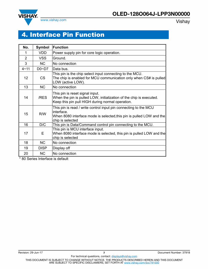
4. Interface Pin Function
No. Symbol Function1 VDD Power supply pin for core logic operation.2 VSS Ground.3 NC No connection
4~11 D0~D7 Data bus.
12 CSThis pin is the chip select input connecting to the MCU.The chip is enabled for MCU communication only when CS# is pulled LOW (active LOW).
13 NC No connection
14 /RESThis pin is reset signal input.When the pin is pulled LOW, initialization of the chip is executed.Keep this pin pull HIGH during normal operation.
15 R/W
This pin is read / write control input pin connecting to the MCU interface.When 8080 interface mode is selected,this pin is pulled LOW and the chip is selected
16 D/C This pin is Data/Command control pin connecting to the MCU.
17 EThis pin is MCU interface input.When 8080 interface mode is selected, this pin is pulled LOW and the chip is selected
18 NC No connection19 DISP Display off20 NC No connection
* 80 Series Interface is default
OLED-128O064J-LPP3N00000www.vishay.com Vishay
Revision: 29-Jun-17 8 Document Number: 37918For technical questions, contact: [email protected]
THIS DOCUMENT IS SUBJECT TO CHANGE WITHOUT NOTICE. THE PRODUCTS DESCRIBED HEREIN AND THIS DOCUMENTARE SUBJECT TO SPECIFIC DISCLAIMERS, SET FORTH AT www.vishay.com/doc?91000
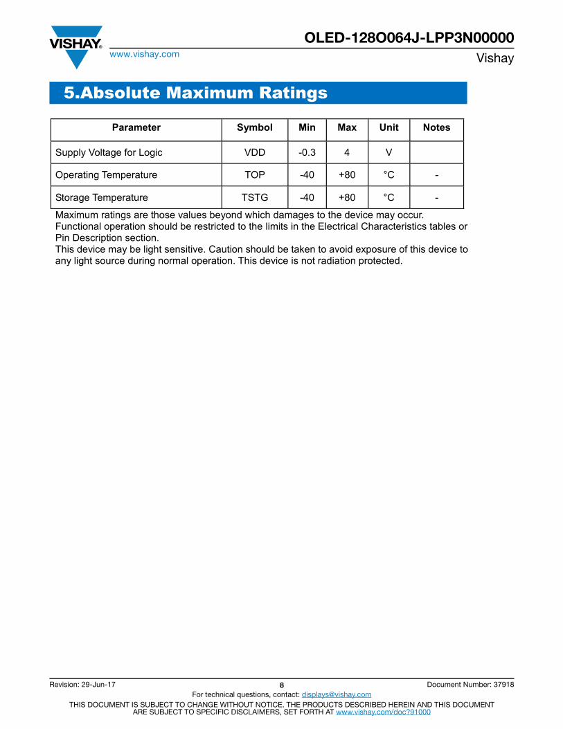
5.Absolute Maximum Ratings
Parameter Symbol Min Max Unit Notes
Supply Voltage for Logic VDD -0.3 4 V
Operating Temperature TOP -40 +80 °C -
Storage Temperature TSTG -40 +80 °C -
Maximum ratings are those values beyond which damages to the device may occur. Functional operation should be restricted to the limits in the Electrical Characteristics tables or Pin Description section.This device may be light sensitive. Caution should be taken to avoid exposure of this device to any light source during normal operation. This device is not radiation protected.

OLED-128O064J-LPP3N00000www.vishay.com Vishay
Revision: 29-Jun-17 9 Document Number: 37918For technical questions, contact: [email protected]
THIS DOCUMENT IS SUBJECT TO CHANGE WITHOUT NOTICE. THE PRODUCTS DESCRIBED HEREIN AND THIS DOCUMENTARE SUBJECT TO SPECIFIC DISCLAIMERS, SET FORTH AT www.vishay.com/doc?91000
6.Electrical Characteristics
Item Symbol Condition Min Typ Max Unit
Supply Voltage for Logic VDD 2.8 3.0 3.3 V
High Level Input VIH 0.8×VDD VLow Level Input VIL 0.2×VDD VHigh Level Output VOH 0.9×VDD VLow Level Output VOL 0.1×VDD V50% Check Board operating Current IDD VDD =3.0V 130 135 150 mA

OLED-128O064J-LPP3N00000www.vishay.com Vishay
Revision: 29-Jun-17 10 Document Number: 37918For technical questions, contact: [email protected]
THIS DOCUMENT IS SUBJECT TO CHANGE WITHOUT NOTICE. THE PRODUCTS DESCRIBED HEREIN AND THIS DOCUMENTARE SUBJECT TO SPECIFIC DISCLAIMERS, SET FORTH AT www.vishay.com/doc?91000
7.Optical Characteristics
Item Symbol Condition Min Typ Max Unit
View Angle(V) 160 deg
(H) 160 deg
Contrast Ratio CR Dark 2000:1
Response TimeT rise 10 s
T fall 10 s
Display with 50% check Board Brightness 80 100 cd/m2
CIEx(Yellow) (CIE1931) 0.45 0.47 0.49
CIEy(Yellow) (CIE1931) 0.48 0.50 0.52

OLED-128O064J-LPP3N00000www.vishay.com Vishay
Revision: 29-Jun-17 11 Document Number: 37918For technical questions, contact: [email protected]
THIS DOCUMENT IS SUBJECT TO CHANGE WITHOUT NOTICE. THE PRODUCTS DESCRIBED HEREIN AND THIS DOCUMENTARE SUBJECT TO SPECIFIC DISCLAIMERS, SET FORTH AT www.vishay.com/doc?91000
8.OLED Lifetime
ITEM Conditions Min Typ Remark
OperatingLife Time
Ta=25/ Initial 50% check board brightness Typical Value
50,000 Hrs Note
Notes:1. Life time is defined the amount of time when the luminance has decayed to <50% of the
initial value.2. This analysis method uses life data obtained under accelerated conditions to extrapolate
an estimated probability density function (pdf) for the product under normal use conditions.3. Screen saving mode will extend OLED lifetime.

OLED-128O064J-LPP3N00000www.vishay.com Vishay
Revision: 29-Jun-17 12 Document Number: 37918For technical questions, contact: [email protected]
THIS DOCUMENT IS SUBJECT TO CHANGE WITHOUT NOTICE. THE PRODUCTS DESCRIBED HEREIN AND THIS DOCUMENTARE SUBJECT TO SPECIFIC DISCLAIMERS, SET FORTH AT www.vishay.com/doc?91000
9.ReliabilityContent of Reliability Test
Environmental Test
Test Item Content of Test Test Condition ApplicableStandard
High Temperature storage
Endurance test applying the high storage temperature for a long time.
80240hrs ——
Low Temperature storage
Endurance test applying the low storage temperature for a long time.
-40240hrs ——
High TemperatureOperation
Endurance test applying the electric stress (Voltage & Current) and the thermal stress to the element for a long time.
80240hrs ——
Low TemperatureOperation
Endurance test applying the electric stress under low temperature for a long time.
-40240hrs ——
High Temperature/Humidity Storage
Endurance test applying the high temperature and high humidity storage for a long time.
60240hrs ——
Temperature Cycle
Endurance test applying the low and high temperature cycle.
-40
30min 5min 30min 1 cycle
-40100 cycles ——
Mechanical Test
Vibration test Endurance test applying the vibration during transportation and using.
10~22Hz 1.5mmp-p22~500Hz 1.5GTotal 0.5hr
——
Shock testConstructional and mechanical endurance test applying the shock during transportation.
50G Half sinwave 11 ms3 times of eachdirection
——
Atmospheric pressure test
Endurance test applying the atmospheric pressure during transportation by air.
115mbar40hrs ——
Others
Static electricity test
Endurance test applying the electric stress to the terminal.
VS=±600V(contact),±800v(air),RS=330CS=150pF10 times
——
*** Supply voltage for OLED system =Operating voltage at 25
OLED-128O064J-LPP3N00000www.vishay.com Vishay
Revision: 29-Jun-17 13 Document Number: 37918For technical questions, contact: [email protected]
THIS DOCUMENT IS SUBJECT TO CHANGE WITHOUT NOTICE. THE PRODUCTS DESCRIBED HEREIN AND THIS DOCUMENTARE SUBJECT TO SPECIFIC DISCLAIMERS, SET FORTH AT www.vishay.com/doc?91000
Test and measurement conditions1. All measurements shall not be started until the specimens attain to temperature stability.
After the completion of the described reliability test, the samples were left at roomtemperature for 2 hrs prior to conducting the failure test at 23±5°C; 55±15% RH.
2. All-pixels-on is used as operation test pattern.3. The degradation of Polarizer are ignored for High Temperature storage, High Temperature/
Humidity Storage, Temperature CycleEvaluation criteria1. The function test is OK.2. No observable defects.3. Luminance: > 50% of initial value.4. Current consumption: within ± 50% of initial value.APPENDIX:RESIDUE IMAGEBecause the pixels are lighted in different time, the luminance of active pixelsmay reduce or differ from inactive pixels. Therefore, the residue image will occur.To avoid the residue image, every pixel needs to be lighted up uniformly.

OLED-128O064J-LPP3N00000www.vishay.com Vishay
Revision: 29-Jun-17 14 Document Number: 37918For technical questions, contact: [email protected]
THIS DOCUMENT IS SUBJECT TO CHANGE WITHOUT NOTICE. THE PRODUCTS DESCRIBED HEREIN AND THIS DOCUMENTARE SUBJECT TO SPECIFIC DISCLAIMERS, SET FORTH AT www.vishay.com/doc?91000
10.Inspection specificationNO Item Criterion AQL01 Electrical
Testing1.1 Missing vertical, horizontal segment, segment contrast defect.1.2 Missing character , dot or icon.1.3 Display malfunction.1.4 No function or no display.1.5 Current consumption exceeds product specifications.1.6 OLED viewing angle defect.1.7 Mixed product types.1.8 Contrast defect.
0.65
02 Black or white spots on OLED(display only)
2.1 White and black spots on display 0.25mm, no more than three white or black spots present.2.2 Densely spaced: No more than two spots or lines within 3mm. 2.5
03 OLEDblack spots, white spots, contamination (non-display)
3.1 Round type : As following drawing
=( x + y ) / 2 SIZE Acceptable Q
TY0.10 Accept no
dense0.10
0.202
0.200.25
1
0.25 0
2.5
3.2 Line type : (As following drawing)Length Width Acceptable Q TY--- W 0.02 Accept no denseL 3.0 0.02 W 0.03
2L 2.5 0.03 W 0.05--- 0.05 W As round type
2.5
04 Polarizer bubbles If bubbles are visible,
judge using black spot specifications, not easy to find, must check in specify direction.
Size Acceptable Q TY0.20 Accept no dense
0.20 0.50 30.50 1.00 21.00 0Total Q TY 3
2.5

OLED-128O064J-LPP3N00000www.vishay.com Vishay
Revision: 29-Jun-17 15 Document Number: 37918For technical questions, contact: [email protected]
THIS DOCUMENT IS SUBJECT TO CHANGE WITHOUT NOTICE. THE PRODUCTS DESCRIBED HEREIN AND THIS DOCUMENTARE SUBJECT TO SPECIFIC DISCLAIMERS, SET FORTH AT www.vishay.com/doc?91000
NO Item Criterion AQL05 Scratches Follow NO.3 OLED black spots, white spots, contamination
06 Chipped glass
Symbols Define:x: Chip length y: Chip width z: Chip thicknessk: Seal width t: Glass thickness a: OLED side lengthL: Electrode pad length:
6.1 General glass chip :6.1.1 Chip on panel surface and crack between panels:
z: Chip thickness y: Chip width x: Chip lengthZ 1/2t Not over viewing
areax 1/8a
1/2t z 2t Not exceed 1/3k x 1/8aIf there are 2 or more chips, x is total length of each chip.
6.1.2 Corner crack:
z: Chip thickness y: Chip width x: Chip lengthZ 1/2t Not over viewing
areax 1/8a
1/2t z 2t Not exceed 1/3k x 1/8aIf there are 2 or more chips, x is the total length of each chip.
2.5

OLED-128O064J-LPP3N00000www.vishay.com Vishay
Revision: 29-Jun-17 16 Document Number: 37918For technical questions, contact: [email protected]
THIS DOCUMENT IS SUBJECT TO CHANGE WITHOUT NOTICE. THE PRODUCTS DESCRIBED HEREIN AND THIS DOCUMENTARE SUBJECT TO SPECIFIC DISCLAIMERS, SET FORTH AT www.vishay.com/doc?91000
NO Item Criterion AQL
06 Glass crack
Symbols :x: Chip length y: Chip width z: Chip thicknessk: Seal width t: Glass thickness a: OLED side lengthL: Electrode pad length6.2 Protrusion over terminal :6.2.1 Chip on electrode pad :
y: Chip width x: Chip length z: Chip thicknessy 0.5mm x 1/8a 0 z t
6.2.2 Non-conductive portion:
y: Chip width x: Chip length z: Chip thickness
y L x 1/8a 0 z tIf the chipped area touches the ITO terminal, over 2/3 of the ITO must remain and be inspected according to electrode terminal specifications.If the product will be heat sealed by the customer, the alignment mark not be damaged.
6.2.3 Substrate protuberance and internal crack.y: width x: lengthy 1/3L x a
2.5

OLED-128O064J-LPP3N00000www.vishay.com Vishay
Revision: 29-Jun-17 17 Document Number: 37918For technical questions, contact: [email protected]
THIS DOCUMENT IS SUBJECT TO CHANGE WITHOUT NOTICE. THE PRODUCTS DESCRIBED HEREIN AND THIS DOCUMENTARE SUBJECT TO SPECIFIC DISCLAIMERS, SET FORTH AT www.vishay.com/doc?91000
Item Criterion AQLCracked glass The OLED with extensive crack is not acceptable. 2.5
Backlight elements
8.1 Illumination source flickers when lit.8.2 Spots or scratched that appear when lit must be judged.
Using OLED spot, lines and contamination standards.8.3 Backlight doesn’t light or color wrong.
0.652.5
0.65
Bezel 9.1 Bezel may not have rust, be deformed or have
fingerprints, stains or other contamination.9.2 Bezel must comply with job specifications.
2.50.65
PCB COB
10.1 COB seal may not have pinholes larger than 0.2mm or contamination.
10.2 COB seal surface may not have pinholes through to the IC.
10.3 The height of the COB should not exceed the height indicated in the assembly diagram.
10.4 There may not be more than 2mm of sealant outside the seal area on the PCB. And there should be no more than three places.
10.5 No oxidation or contamination PCB terminals.10.6 Parts on PCB must be the same as on the production
characteristic chart. There should be no wrong parts, missing parts or excess parts.
10.7 The jumper on the PCB should conform to the product characteristic chart.
10.8 If solder gets on bezel tab pads, OLED pad, zebra pad or screw hold pad, make sure it is smoothed down.
2.5
2.50.65
2.5
2.50.65
0.65
2.5
Soldering
11.1 No un-melted solder paste may be present on the PCB.11.2 No cold solder joints, missing solder connections,
oxidation or icicle.11.3 No residue or solder balls on PCB.11.4 No short circuits in components on PCB.
2.52.5
2.50.65

OLED-128O064J-LPP3N00000www.vishay.com Vishay
Revision: 29-Jun-17 18 Document Number: 37918For technical questions, contact: [email protected]
THIS DOCUMENT IS SUBJECT TO CHANGE WITHOUT NOTICE. THE PRODUCTS DESCRIBED HEREIN AND THIS DOCUMENTARE SUBJECT TO SPECIFIC DISCLAIMERS, SET FORTH AT www.vishay.com/doc?91000
NO Item Criterion AQL
12 General appearance
12.1 No oxidation, contamination, curves or, bends on interface Pin (OLB) of TCP.
12.2 No cracks on interface pin (OLB) of TCP.12.3 No contamination, solder residue or solder balls on
product.12.4 The IC on the TCP may not be damaged, circuits.12.5 The uppermost edge of the protective strip on the
interface pin must be present or look as if it cause the interface pin to sever.
12.6 The residual rosin or tin oil of soldering (component or chip component) is not burned into brown or black color.
12.7 Sealant on top of the ITO circuit has not hardened.12.8 Pin type must match type in specification sheet.12.9 OLED pin loose or missing pins.12.10 Product packaging must the same as specified on
packaging specification sheet.12.11 Product dimension and structure must conform to
product specification sheet.
2.5
0.652.52.52.5
2.5
2.50.650.650.65
0.65
OLED-128O064J-LPP3N00000www.vishay.com Vishay
Revision: 29-Jun-17 19 Document Number: 37918For technical questions, contact: [email protected]
THIS DOCUMENT IS SUBJECT TO CHANGE WITHOUT NOTICE. THE PRODUCTS DESCRIBED HEREIN AND THIS DOCUMENTARE SUBJECT TO SPECIFIC DISCLAIMERS, SET FORTH AT www.vishay.com/doc?91000
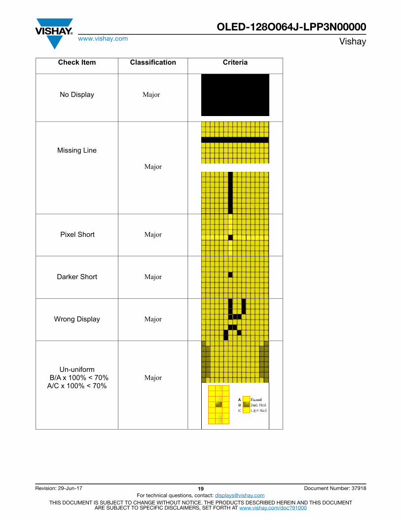
Check Item Classification Criteria
No Display Major
Missing Line
Major
Pixel Short Major
Darker Short Major
Wrong Display Major
Un-uniformB/A x 100% < 70%
A/C x 100% < 70%Major

OLED-128O064J-LPP3N00000www.vishay.com Vishay
Revision: 29-Jun-17 20 Document Number: 37918For technical questions, contact: [email protected]
THIS DOCUMENT IS SUBJECT TO CHANGE WITHOUT NOTICE. THE PRODUCTS DESCRIBED HEREIN AND THIS DOCUMENTARE SUBJECT TO SPECIFIC DISCLAIMERS, SET FORTH AT www.vishay.com/doc?91000
11.Precautions in use of OLED ModulesModules
(1)Avoid applying excessive shocks to module or making any alterations or modifications to it.(2)Don’t make extra holes on the printed circuit board, modify its shape or change the
components of OLED display module.(3)Don’t disassemble the OLED display module.(4)Don’t operate it above the absolute maximum rating.(5)Don’t drop, bend or twist OLED display module.(6)Soldering: only to the I/O terminals.(7)Storage: please storage in anti-static electricity container and clean environment.(8)It's pretty common to use "Screen Saver" to extend the lifetime and Don't use fix information
for long time in real application. (9)Don't use fixed information in OLED panel for long time, that will extend "screen burn" effect
time..(10) Vishay has the right to change the passive components, including R2and R3 adjust resistors.
(Resistors, capacitors and other passive components will have different appearance and color caused by the different supplier.)
(11) Vishay have the right to change the PCB Rev. (In order to satisfy the supplying stability, management optimization and the best product performance...etc, under the premise of not affecting the electrical characteristics and external dimensions, Vishay have the right to modify the version.)
11.1. Handling Precautions(1) Since the display panel is being made of glass, do not apply mechanical impacts such us
dropping from a high position.(2) If the display panel is broken by some accident and the internal organic substance leaks out,
be careful not to inhale nor lick the organic substance.(3) If pressure is applied to the display surface or its neighborhood of the OLED display module,
the cell structure may be damaged and be careful not to apply pressure to these sections.(4) The polarizer covering the surface of the OLED display module is soft and easily scratched.
Please be careful when handling the OLED display module.(5) When the surface of the polarizer of the OLED display module has soil, clean the surface. It
takes advantage of by using following adhesion tape.* Scotch Mending Tape No. 810 or an equivalentNever try to breathe upon the soiled surface nor wipe the surface using cloth containing
solventsuch as ethyl alcohol, since the surface of the polarizer will become cloudy.Also, pay attention that the following liquid and solvent may spoil the polarizer:* Water* Ketone* Aromatic Solvents
(6) Hold OLED display module very carefully when placing OLED display module into the System housing. Do not apply excessive stress or pressure to OLED display module. And, do not over bend the film with electrode pattern layouts.These stresses will influence the display performance. Also, secure sufficient rigidity for theouter cases.

OLED-128O064J-LPP3N00000www.vishay.com Vishay
Revision: 29-Jun-17 21 Document Number: 37918For technical questions, contact: [email protected]
THIS DOCUMENT IS SUBJECT TO CHANGE WITHOUT NOTICE. THE PRODUCTS DESCRIBED HEREIN AND THIS DOCUMENTARE SUBJECT TO SPECIFIC DISCLAIMERS, SET FORTH AT www.vishay.com/doc?91000
(7) Do not apply stress to the LSI chips and the surrounding molded sections.(8) Do not disassemble nor modify the OLED display module.(9) Do not apply input signals while the logic power is off.(10) Pay sufficient attention to the working environments when handing OLED displaymodules to prevent occurrence of element breakage accidents by static electricity.* Be sure to make human body grounding when handling OLED display modules.* Be sure to ground tools to use or assembly such as soldering irons.* To suppress generation of static electricity, avoid carrying out assembly work under dry
environments.* Protective film is being applied to the surface of the display panel of the OLED displaymodule. Be careful since static electricity may be generated when exfoliating the protectivefilm.(11) Protection film is being applied to the surface of the display panel and removes the protection film before assembling it. At this time, if the OLED display module has been stored for a long period of time, residue adhesive material of the protection film may remain on thesurface of the display panel after removed of the film. In such case, remove the residuematerial by the method introduced in the above Section 5.(12) If electric current is applied when the OLED display module is being dewed or when it isplaced under high humidity environments, the electrodes may be corroded and be careful toavoid the above.11.2. Storage Precautions(1) When storing OLED display modules, put them in static electricity preventive bagsavoiding exposure to direct sun light nor to lights of fluorescent lamps. and, also, avoidinghigh temperature and high humidity environment or low temperature (less than 0°C) environments.(We recommend you to store these modules in the packaged state when they were shippedfrom Vishay.At that time, be careful not to let water drops adhere to the packages or bags nor let dewing
occur with them.(2) If electric current is applied when water drops are adhering to the surface of the OLEDdisplay module, when the OLED display module is being dewed or when it is placed underhigh humidity environments, the electrodes may be corroded and be careful about the above.11.3. Designing Precautions(1) The absolute maximum ratings are the ratings which cannot be exceeded for OLEDdisplay module, and if these values are exceeded, panel damage may be happen.(2) To prevent occurrence of malfunctioning by noise, pay attention to satisfy the VIL and VIHspecifications and, at the same time, to make the signal line cable as short as possible.(3) We recommend you to install excess current preventive unit (fuses, etc.) to the powercircuit (VDD). (Recommend value: 0.5A)(4) Pay sufficient attention to avoid occurrence of mutual noise interference with theneighboring devices.(5) As for EMI, take necessary measures on the equipment side basically.

OLED-128O064J-LPP3N00000www.vishay.com Vishay
Revision: 29-Jun-17 22 Document Number: 37918For technical questions, contact: [email protected]
THIS DOCUMENT IS SUBJECT TO CHANGE WITHOUT NOTICE. THE PRODUCTS DESCRIBED HEREIN AND THIS DOCUMENTARE SUBJECT TO SPECIFIC DISCLAIMERS, SET FORTH AT www.vishay.com/doc?91000
(6) When fastening the OLED display module, fasten the external plastic housing section.(7) If power supply to the OLED display module is forcibly shut down by such errors as takingout the main battery while the OLED display panel is in operation, we cannot guarantee thequality of this OLED display module.* Connection (contact) to any other potential than the above may lead to rupture of
the IC.11.4. Precautions when disposing of the OLED display modules1) Request the qualified companies to handle industrial wastes when disposing of the OLED
display modules. Or, when burning them, be sure to observe the environmental and hygienic laws and regulations.
11.5. Other Precautions(1) When an OLED display module is operated for a long of time with fixed pattern may remain
as an after image or slight contrast deviation may occur.Nonetheless, if the operation is interrupted and left unused for a while, normal state can be
restored. Also, there will be no problem in the reliability of the module.(2) To protect OLED display modules from performance drops by static electricity rapture, etc.,
do not touch the following sections whenever possible while handling the OLED display modules.
* Pins and electrodes* Pattern layouts such as the TCP & FPC(3) With this OLED display module, the OLED driver is being exposed. Generally speaking,
semiconductor elements change their characteristics when light is radiated according to the principle of the solar battery. Consequently, if this OLED driver is exposed to light, malfunctioning may occur.
* Design the product and installation method so that the OLED driver may be shielded from light in actual usage.
* Design the product and installation method so that the OLED driver may be shielded from light during the inspection processes.
(4) Although this OLED display module stores the operation state data by the commands and the indication data, when excessive external noise, etc. enters into the module, the internal status may be changed. It therefore is necessary to take appropriate measures to suppress noise generation or to protect from influences of noise on the system design.
(5) We recommend you to construct its software to make periodical refreshment of the operation statuses (re-setting of the commands and re-transference of the display data) to cope with catastrophic noise.
(6)Resistors, capacitors and other passive components will have different appearance and color caused by the different supplier.
(7)Our company will has the right to upgrade and modify the product function.

Legal Disclaimer Noticewww.vishay.com Vishay
Revision: 08-Feb-17 1 Document Number: 91000
DisclaimerALL PRODUCT, PRODUCT SPECIFICATIONS AND DATA ARE SUBJECT TO CHANGE WITHOUT NOTICE TO IMPROVE RELIABILITY, FUNCTION OR DESIGN OR OTHERWISE.
Vishay Intertechnology, Inc., its affiliates, agents, and employees, and all persons acting on its or their behalf (collectively, “Vishay”), disclaim any and all liability for any errors, inaccuracies or incompleteness contained in any datasheet or in any other disclosure relating to any product.
Vishay makes no warranty, representation or guarantee regarding the suitability of the products for any particular purpose or the continuing production of any product. To the maximum extent permitted by applicable law, Vishay disclaims (i) any and all liability arising out of the application or use of any product, (ii) any and all liability, including without limitation special, consequential or incidental damages, and (iii) any and all implied warranties, including warranties of fitness for particular purpose, non-infringement and merchantability.
Statements regarding the suitability of products for certain types of applications are based on Vishay’s knowledge of typical requirements that are often placed on Vishay products in generic applications. Such statements are not binding statements about the suitability of products for a particular application. It is the customer’s responsibility to validate that a particular product with the properties described in the product specification is suitable for use in a particular application. Parameters provided in datasheets and / or specifications may vary in different applications and performance may vary over time. All operating parameters, including typical parameters, must be validated for each customer application by the customer’s technical experts. Product specifications do not expand or otherwise modify Vishay’s terms and conditions of purchase, including but not limited to the warranty expressed therein.
Except as expressly indicated in writing, Vishay products are not designed for use in medical, life-saving, or life-sustaining applications or for any other application in which the failure of the Vishay product could result in personal injury or death. Customers using or selling Vishay products not expressly indicated for use in such applications do so at their own risk. Please contact authorized Vishay personnel to obtain written terms and conditions regarding products designed for such applications.
No license, express or implied, by estoppel or otherwise, to any intellectual property rights is granted by this document or by any conduct of Vishay. Product names and markings noted herein may be trademarks of their respective owners.
© 2017 VISHAY INTERTECHNOLOGY, INC. ALL RIGHTS RESERVED