Embed Size (px)
Citation preview

Iron (III) Chloride Doping of Large-Area Chemical Vapor DepositionGraphene
ARCHNESBy MASSACHUSETTS IN~TT
OF TECHNOLOGY
Yi Song JUL 0 8 2013B.S. Electrical Engineering
University of California, Berkeley 2011 LIBRARIES
SUBMITTED TO THE DEPARTMENT OFELECTRICAL ENGINEERING AND COMPUTER SCIENCE
IN PARTIAL FULFILLMENT OF THE REQUIREMENTS FOR THE DEGREE OFMASTER OF SCIENCE IN ELECTRICAL ENGINEERING
AT THEMASSACHUSETTS INSTITUTE OF TECHNOLOGY
JUNE 2013
C2013 Massachusetts Institute of Technology. All rights reserved.
Author: .............. Department of Electrical EngineeringMay 21, 2013
Certified by: .......................................Professor Jing Kong
Associate Professor of Electrical EngineeringThesis Supervisor
Accepted by: .............................. ............Pr~fess j/)slie A. Kolodziej ski
Graduate Officer, Professor of Electrical Engineering

2

Iron (III) Chloride Doping of Large-Area Chemical Vapor Deposition
Graphene
By
Yi Song
Submitted to the Department of Electrical Engineering and Computer ScienceOn May 21, 2013, in partial fulfillment of the
requirements for the degree ofMaster of Science
Abstract
Chemical doping is an effective method of reducing the sheet resistance of graphene. This thesisaims to develop an effective method of doping large area Chemical Vapor Deposition (CVD)graphene using Iron (1II) Chloride (FeCl 3). It is shown that evaporating FeCl3 can increase thecarrier concentration of monolayer graphene to greater than 7x1 0 3 CM2 and achieve resistancesas low 72t2/sq. We also evaluate other important properties of the doped graphene such assurface cleanliness, air stability, and solvent stability. Furthermore, we compare FeCl 3 to threeother common dopants: Gold (III) Chloride (AuCl3), Nitric Acid (I-N0 3), and TFSA((CF 3SO2)2NH). We show that compared to these dopants, FeCl 3 can not only achieve bettersheet resistance but also has other key advantages including better solvent stability and betterheat stability.
Thesis Supervisor: Jing Kong
Title: Associate Professor of Electrical Engineering
3

4

Contents
S Introduction............................................................................................................................ 9
1.1 Background in Graphene Doping ................................................................................. 9
1.2 Scope of This W ork.................................................................................................... 10
2 Background in G raphene .................................................................................................. 11
2.1 Sheet Resistance Considerations ................................................................................. 11
2.2 Synthesis and Transfer................................................................................................ 12
2.2.1 Grow th..................................................................................................................... 12
2.2.2 Transfer ................................................................................................................... 13
2.2.3 PM M A Rem oval ................................................................................................. 13
3 D oping CV D G raphene w ith FeC13 ........................................... . . . . . . . . . . . . . . . . . . . . . . . .. . . . . . . . . . . . . . 15
3.1 Procedure ........................................................................................................................ 15
3.1.1 Initial Tests.............................................................................................................. 15
3.1.2 3.1.2 Optim ized Procedure.................................................................................. 16
3.1.3 Other M odifications and Considerations............................................................. 17
3.2 Characterization of FeCl3 Doped Graphene ............................................................... 18
3.2.1 Sheet Resistance and Carrier Concentration ........................................................ 18
3.2.2 Surface Cleanliness ............................................................................................. 20
3.2.3 Stability in Solvents ............................................................................................. 21
3.2.4 Stability in A ir...................................................................................................... 22
3.2.5 Effectiveness in M ulti-layer Sam ples ................................................................. 24
3.2.6 Ram an Signature ................................................................................................. 25
4 C om parison of D oping M ethods...................................................................................... 27
4.1 Com m on D opants...................................................................................................... 27
5

4.2 Points of Comparison................................................................................................. 28
4.2.1 Sheet Resistance and Carrier Concentration ........................................................ 28
4.2.2 Stability in Atmosphere...................................................................................... 30
4.2.3 Stability in Solvents ............................................................................................ 33
4.2.4 Other Considerations........................................................................................... 34
5 Summary and Conclusions . . .. . . ... .. . ............................................. 37
R eferences .................................................................................................................................... 3 9
6

List of Figures
Figure 2-1. System used for synthesis of CVD graphene on copper foil. Components are roughlyto sca le ........................................................................................................................................... 12
Figure 2-2. Transfer of graphene onto SiO 2 using PMMA as an intermediate membrane.....13
Figure 3-1. Basic system for FeCl 3 doping. Components are drawn roughly to scale..............15Figure 3-2. Graphene after 1h in FeCl3 vapor at high temperatures. ......................................... 16Figure 3-3. FeCl3 condensed on graphene surface................................................................... 17Figure 3-4. Schematic of mass production doping system. Drawing not to scale. .................... 18Figure 3-5. Histogram of the sheet resistance of FeCl3-doped graphene................. 19Figure 3-6. Histogram of the carrier concentration of FeCl3-doped graphene.............19Figure 3-7. Graphene cleanly doped with FeCl 3 ................................ . . .. . . . . . . . . . . . . . . . . . . . . . . . . . . . . . 20Figure 3-8. a,b) SEM of an FeCl3 doped graphene sample that looks clean under optical
microscope. c,d) Sample that looks dirty visually. .................................................................. 21
Figure 3-9. Time evolution of the electrical properties of FeCl 3 doped graphene. The data is
averaged over three sam ples ..................................................................................................... 23Figure 3-10. Change in sheet resistance of FeCl3 doped graphene over time at higher
tem p eratu res..................................................................................................................................24Figure 3-11. Sheet resistance and carrier concentration for multilayer FeCl 3 doped graphenesam p le s..........................................................................................................................................2 5Figure 3-12. Raman spectrum of FeCl3-doped graphene compared to pristine graphene. ........... 26
Figure 4-1. Sheet resistance versus layer number for all dopants............................................. 28Figure 4-2. Carrier concentration versus layer number for all dopants. .................................. 29Figure 4-3. Absolute sheet resistance for all dopants over time. .............................................. 30Figure 4-4. Relative sheet resistance for all dopants over time (normalized to initial value).......30Figure 4-5. Absolute carrier concentration for all dopants over time. ....................................... 31
Figure 4-6. Relative carrier concentration for all dopants over time (normalized to initial value).
....................................................................................................................................................... 3 1
Figure 4-7. Time evolution of sheet resistance for all dopants at 130C.................................... 32Figure 4-8. Percent change in resistance. Broken samples are shown with dotted lines. ......... 34
Figure 4-9. Sheet resistance and carrier concentration comparison for acetone treatment and
an n ealin g ....................................................................................................................................... 3 5Figure 4-10. Optical images of AuCl 3 doped graphene. a) Annealed sample. b) Acetone-treated
sample. The bright particles present on the acetone-treated graphene cause the surface of the
graphene to appear dull by eye.................................................................................................. 36
7

List of Tables
Table 3-1. Change in sheet resistance and carrier concentration of FeCl 3 doped graphene afterim m ersion in various solvents................................................................................................... 22Table 4-1. Sheet resistance achieved by various dopants, as reported in literature. ................. 27Table 4-2. Percentage increase in sheet resistance.................................................................... 33Table 4-3. Percentage change in carrier concentration. ........................................................... 33
8
Chapter 1
1 Introduction
1.1 Background in Graphene Doping
Because of its high electrical conductance, high optical transmittance and excellentflexibility, graphene has attracted much attention in the field of flexible optoelectronics.Chemical Vapor Deposition (CVD) growth on copper allows for mass production of large areamonolayer graphene suitable for electrodes in optoelectronic devices 1. However, monolayergraphene typically has sheet resistance of several hundred ohms, which is significantly higherthan that of Indium Tin Oxide (ITO), which is the industry standard 2. This can introduce asignificant series resistance in solar cells or LEDs and will inevitably degrade deviceperformances. Stacking multiple layers of graphene does improve the overall resistance at theexpense of optical transmittance3 ' 4 . Even with multiple layers, however, the I-V curves of CVDgraphene-based devices show significant series resistances and the efficiency of these devicesremain inferior to that of their ITO-based counterparts3 . Furthermore, the process of transferringgraphene layer-by-layer is time consuming and the resistance does not always scale linearly withthe number of layers5 ,6 .
Another common method to improve the resistance of graphene electrodes is chemicaldoping. P-type dopants can substantially improve the conductivity of graphene with little impactin optical transmittance. Currently, the most commonly-used dopants are Gold Chloride (AuCl 3)and Nitric Acid (HNO 3). Kim et al. demonstrated that AuCl 3 can reduce the resistance ofmonolayer graphene by up to 77% to 150K/sq 7. Bae et al. reported similar results using HNO 3,reducing the resistance by 60% to 125Q/sq 6. However, both types of doping are unstable in air;the sheet resistance increases quickly over the first few days and eventually saturates at roughly200% of the resistance immediately after doping"' 9 . Furthermore, AuCl3 leaves gold particles upto 1 00nm in diameter on the surface of the graphene, which can cause shorts in thin-film verticaldevices 7. Other dopants include bis(trifluoromethanesulfonyl)amide (TFSA), which was used toachieve 8.6% efficiency in graphene/n-Si Schottky solar cells, and tetracyanoquinodimethane(TCNQ), which his compatible with layer-by-layer graphene transfer. Both of these also havedisadvantages, as TCNQ requires a lengthy evaporation process and TFSA - though stable in air- also leaves residues and dissolves in common solvents such as Isopropanol. An ideal dopantfor CVD graphene will have the following characteristics:
1. Can achieve low sheet resistance2. Stable in atmosphere3. Stable in solvents (water, IPA, Acetone, etc)4. Clean5. Fast6. Economic7. Compatible with multi-layer transfer
9

Unfortunately, it is highly unlikely that any dopant can exhibit all of these characteristics sothe most appropriate one must be selected based on the particular application.
In 2012, Khrapach et al. demonstrated that intercalation doping on exfoliated graphene usingIron (III) Chloride (FeCl3) can achieve resistances as low as 8.8Q/sq at 84% transmittance with5-layer graphene 10. Furthermore, this type of doping is stable in air for up to one year. However,HOPG graphene cannot be mass-produced and therefore cannot be used for large-area practicaloptoelectronic devices. To make matters worse, the doping process entails pumping a sealedchamber down to 2x 10⁴ mbar, which requires a turbo pump and, and the intercalation processtakes 10h. Nonetheless, this work highlights the advantages of FeCl3 doping over other methodsand may be promising if applied to CVD graphene.
1.2 Scope of This Work
The goal of this thesis is to twofold: first, we refine the process of FeCl 3 doping for CVDgraphene characterize the results. Next, we compare the effectiveness of FeCl3 to other dopantsbased on the aforementioned metrics. Chapter 2 offers an overview of graphene, in particular, itssynthesis and transfer and how these processes affect the sheet resistance. Chapter 3 discussesthe doping procedure itself, including what works and what does not work, and evaluatescharacteristics of FeCl 3-doped graphene. Chapter 4 brings into the discussion three additionaldopants: Gold(III) Chloride (AuCl3), Nitric Acid (HNO 3), and TFSA. FeCl3 is compared to thesedopants in terms of the important metrics and it is shown that FeCl3 has some key advantagesand disadvantages. Chapter 5 provides a summary of our findings and some additionaldiscussion.
10

Chapter 2
2 Background in Graphene
2.1 Sheet Resistance Considerations
The sheet resistance of graphene is determined by two parameters: carrier mobility ([t),measured in cm 2/Vs and sheet carrier concentration (n), measured in cm-2. These parameters arerelated to the sheet resistance by the following expression.
Rkh = 1 (1)q/pn
Theoretical calculations suggest that in intrinsic graphene, the mobility at carrier density of1012cm-2 is as high as 200 OOOcm 2/Vs at room temperature, which yields sheet resistance of300hms". This is equivalent to 108S/m in three-dimensional conductivity, which is superior tothat of aluminum or copper. However, the 300hms result assumes flat, suspended, single-crystalline graphene in vacuum, in which case only electron-phonon scattering contributes toresistance. In practice, numerous additional sources of scattering such as wrinkles, domainboundaries, substrate interactions, and charged impurities make it difficult to achieve this200000cm 2/Vs figure, especially for large area CVD graphene.
Thus, an alternative strategy for lowering the resistance of graphene is to dope it as heavilyas possible. It is clear from the above expression that in order to minimize resistance, we shouldmaximize both mobility and carrier concentration. However, increasing carrier concentration viadoping inevitably increases charge impurity scattering, thus degrading mobility according to theDrude model. In fact, if the carrier concentration is high enough, charged impurity scatteringbecomes the dominant scattering source and other sources such as substrate interactions nolonger matter. However, it is possible for the doping process to introduce defects in the graphene,which further reduces effective mobility. Thus, the goal of doping should be to increase carrierconcentration as much as possible while minimizing the decrease in mobility.
The sheet resistance can be measured using Van der Pauw's method, which entails I/Vmeasurements from a series of four contacts placed on the periphery of the sample. The carrierconcentration can be determined using four probe Hall measurements. The mobility of thesample can be derived from the results of the two measurements. In this work, all sheetresistance and carrier concentration measurements are performed using a home-built four-point-probe station and a 2000Gs permanent magnet.
11

2.2 Synthesis and Transfer
Although the synthesis and transfer of CVD graphene is not the focus of this work, it is quitea sensitive process with details pertinent to doping.
2.2.1 Growth
The graphene used in this work is synthesized using Low-Pressure Chemical VaporDeposition (LPCVD) on copper foil'2 . The schematic of the system is shown in Figure 2-1.Growth on copper foil produces a uniform monolayer, as opposed to growing on nickel, whichproduces non-uniform multilayer graphene 13. Before growth, the copper foil was cleaned bysonicating in nickel etchant (type TBP) for 30s and rinsing with DI water. After cleaning, thecopper foil was placed in a quartz tube and annealed at 1000"C for 30min while flowing 10sccmH2. Graphene was then grown for 30min by increasing H2 flow rate to 70sccm and setting theCH4 flow rate 0.5sccm. The chamber pressure was 400mTorr during the annealing phase and1.90Torr during the growth phase. The influence of growth variables such as gas flow rates,partial pressures, and temperature on the quality of graphene is beyond the scope of this work.However, from our experiences, the resistance of the graphene film is not strongly dependent ongrowth conditions, with 0.5sccm CH 4 and 70sccm H2 producing similar results as 20sccm CH4and 1 Osccm H2 .
Figure 2-1. System used for synthesis of CVD graphene on copper foil. Components are roughly to scale.
12
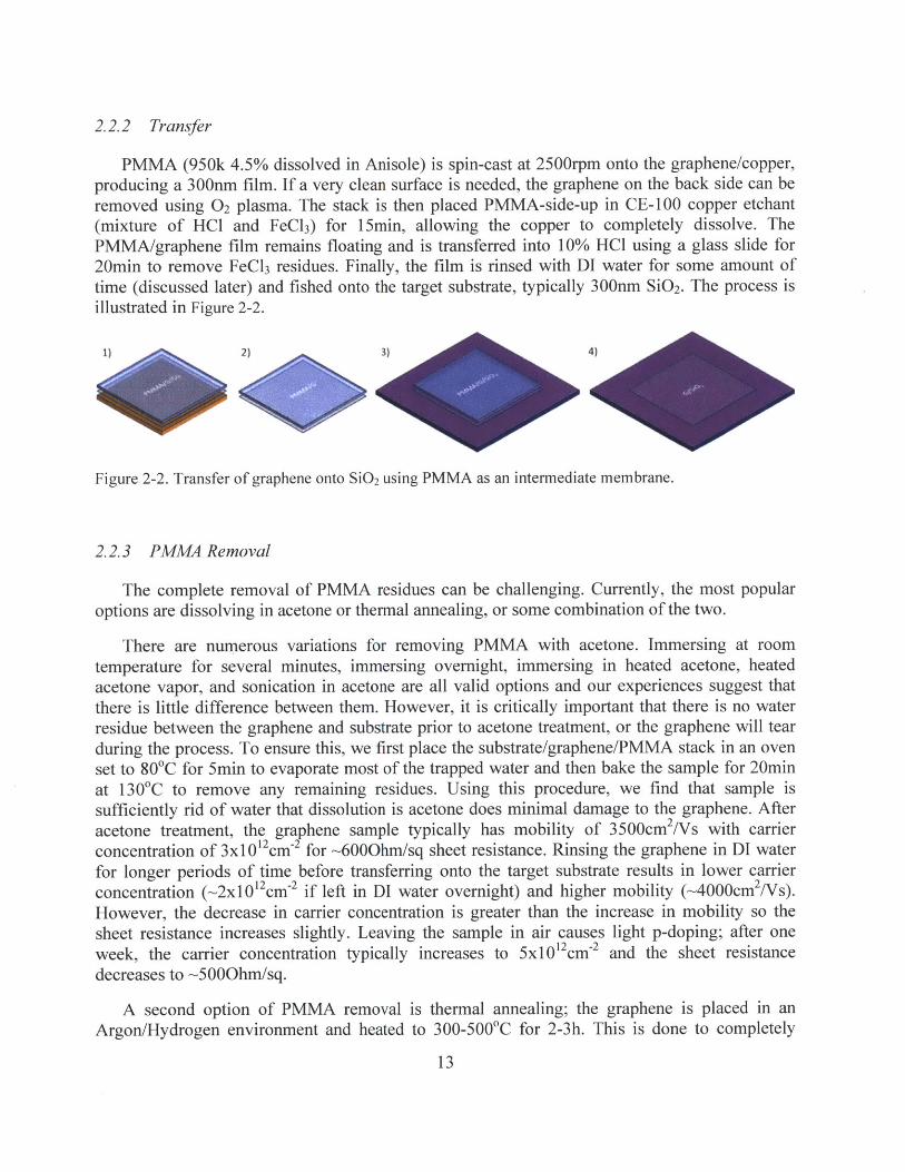
2.2.2 Transfer
PMMA (950k 4.5% dissolved in Anisole) is spin-cast at 2500rpm onto the graphene/copper,producing a 300nm film. If a very clean surface is needed, the graphene on the back side can beremoved using 02 plasma. The stack is then placed PMMA-side-up in CE-100 copper etchant(mixture of HCl and FeCl3) for 15min, allowing the copper to completely dissolve. ThePMMA/graphene film remains floating and is transferred into 10% HCl using a glass slide for20min to remove FeCl 3 residues. Finally, the film is rinsed with DI water for some amount oftime (discussed later) and fished onto the target substrate, typically 300nm SiO2. The process isillustrated in Figure 2-2.
Figure 2-2. Transfer of graphene onto SiO 2 using PMMA as an intermediate membrane.
2.2.3 PMMA Removal
The complete removal of PMMA residues can be challenging. Currently, the most popularoptions are dissolving in acetone or thermal annealing, or some combination of the two.
There are numerous variations for removing PMMA with acetone. Immersing at roomtemperature for several minutes, immersing overnight, immersing in heated acetone, heatedacetone vapor, and sonication in acetone are all valid options and our experiences suggest thatthere is little difference between them. However, it is critically important that there is no waterresidue between the graphene and substrate prior to acetone treatment, or the graphene will tearduring the process. To ensure this, we first place the substrate/graphene/PMMA stack in an ovenset to 800C for 5min to evaporate most of the trapped water and then bake the sample for 20minat 130"C to remove any remaining residues. Using this procedure, we find that sample issufficiently rid of water that dissolution is acetone does minimal damage to the graphene. Afteracetone treatment, the graphene sample typically has mobility of 3500cm 2/Vs with carrierconcentration of 3x1 0 12 cm2 for ~6000hm/sq sheet resistance. Rinsing the graphene in DI waterfor longer periods of time before transferring onto the target substrate results in lower carrierconcentration (~2xl01cm 2 if left in DI water overnight) and higher mobility (~4000cm 2/Vs).However, the decrease in carrier concentration is greater than the increase in mobility so thesheet resistance increases slightly. Leaving the sample in air causes light p-doping; after oneweek, the carrier concentration typically increases to 5x 1012 cm2 and the sheet resistancedecreases to ~5000hm/sq.
A second option of PMMA removal is thermal annealing; the graphene is placed in anArgon/Hydrogen environment and heated to 300-500"C for 2-3h. This is done to completely
13
2,14remove PMMA residues, leaving a clean surface for further processing . Typically, this step isadded after acetone treatment but can be performed directly after transfer at the expense ofleaving more PMMA residues 2. However, the high temperature causes the graphene to conformmore closely to the underlying SiO 2, which results in hole doping and degraded mobility". Insome cases, the hit on electrical performance is undesirable but in the case of conductingelectrodes, the increase in carrier concentration outweighs the reduction in mobility, resulting inan overall decrease in sheet resistance. Typical values after annealing are 2000cm 2/Vs mobilityand 1xIO13cm-2 carrier concentration for -30OOhm sheet resistance. It is worth noting, however,that the extra scattering term associated with increased surface roughness also affects carriersintroduced via chemical doping. In other words, we expect that a chemically doped, annealedsample would have worse mobility than a similarly doped sample that has only received acetonetreatment. However, as previously mentioned, for chemically doped samples, the dominantscattering mechanism is charge impurity scattering, so it is uncertain whether roughnessscattering plays a key role in determining the final sheet resistance. We briefly investigate thiseffect in this work.
There exists other for removing PMMA residues. Scanning the graphene surface with anatomic force microscope (AFM) tip also cleans it, but this method is obviously impractical forlarge areas6 ' 17. Chloroform and formamide have been shown to lower the intrinsic doping levelbetter than acetone' 5 18 . From our experiences, nitromethane is also more effective than acetonein removing PMMA, but it is not clear if nitromethane immersion has any unwanted side effects.Thus, to minimize the number of unknowns, we only consider acetone treatment and annealing.
14

Chapter 3
3 Doping CVD Graphene with FeC13
3.1 Procedure
3.1.1 Initial Tests
The graphene (on SiO 2) and FeCl3 (anhydrous 98% acquired from Alfa Aesar) were placed ina glass pipette and pumped down using a dry scroll pump. Because of equipment limitations, theminimum pressure achieved was 40mTorr. After base pressure is reached, a blow torch is used toseal the pipette. After giving the pipette sufficient time to cool, the graphene sample was slid inthe pipette to a position ~10cm from the FeCl3. The pipette was then placed in a tube ovenheated to 360"C with the graphene sample in the middle and the FeCl 3 at the periphery, as shownin Figure 3-1. The temperature at the FeCl3 location was measured to be 320"C. After 10h, thepipette was broken and the sample was removed.
Figure 3-1. Basic system for FeCb doping. Components are drawn roughly to scale.
For all doping attempts using the conditions outlined above, upon breaking the pipette, wefind that the graphene is completely broken. Thus, the parameters used by Krapach et al. forexfoliated graphene does not appear to work for CVD graphene. Exposing CVD graphene toFeCl 3 at 3600C for longer periods of time under vacuum causes the graphene to break andcrumple on the substrate; this occurs regardless of whether the graphene was annealed or not.This result is not surprising because CVD graphene is inherently polycrystalline, which allows
15

for FeCl 3 to penetrate underneath through the domain boundaries and strip the graphene from thesubstrate. As shown in Figure 3-2, lowering the temperature to 320"C or 280"C does help buteven at these lower temperatures, the graphene is still broken.
Figure 3-2. Graphene after Ih in FeCl 3 vapor at high temperatures.
3.1.2 Optimized Procedure
After a trial-and-error process, we find that doping in atmosphere in the temperature range of3200 C - 360*C for a short amount of time (1-5min) produces unbroken graphene with excellentsheet resistance (~1000hm/sq). Lower temperatures for longer times, such as 240"C for 1 h, alsostrongly dopes the graphene, but tends to leaves more residues, presumably due to the longeramount of time the graphene is left in the vessel.
Ambient pressure is selected over low pressure because the FeCl3 evaporates more quicklyunder vacuum, making the reaction more difficult to control. Furthermore, sealing under ambientpressure does not require a vacuum pump, making the process more economic. From ourexperiences, heating graphene to 360"C in atmosphere for longer times (1 hour) severely
16
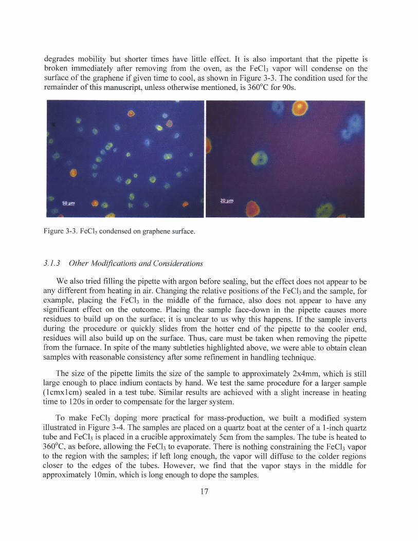
degrades mobility but shorter times have little effect. It is also important that the pipette isbroken immediately after removing from the oven, as the FeCl 3 vapor will condense on thesurface of the graphene if given time to cool, as shown in Figure 3-3. The condition used for theremainder of this manuscript, unless otherwise mentioned, is 360"C for 90s.
Figure 3-3. FeCl 3 condensed on graphene surface.
3.1.3 Other Modifications and Considerations
We also tried filling the pipette with argon before sealing, but the effect does not appear to beany different from heating in air. Changing the relative positions of the FeCl 3 and the sample, forexample, placing the FeCl 3 in the middle of the furnace, also does not appear to have anysignificant effect on the outcome. Placing the sample face-down in the pipette causes moreresidues to build up on the surface; it is unclear to us why this happens. If the sample invertsduring the procedure or quickly slides from the hotter end of the pipette to the cooler end,residues will also build up on the surface. Thus, care must be taken when removing the pipettefrom the furnace. In spite of the many subtleties highlighted above, we were able to obtain cleansamples with reasonable consistency after some refinement in handling technique.
The size of the pipette limits the size of the sample to approximately 2x4mm, which is stilllarge enough to place indium contacts by hand. We test the same procedure for a larger sample(1cmxlcm) sealed in a test tube. Similar results are achieved with a slight increase in heatingtime to 120s in order to compensate for the larger system.
To make FeCl 3 doping more practical for mass-production, we built a modified systemillustrated in Figure 3-4. The samples are placed on a quartz boat at the center of a 1-inch quartztube and FeCl 3 is placed in a crucible approximately 5cm from the samples. The tube is heated to3600C, as before, allowing the FeCl 3 to evaporate. There is nothing constraining the FeCl 3 vaporto the region with the samples; if left long enough, the vapor will diffuse to the colder regionscloser to the edges of the tubes. However, we find that the vapor stays in the middle forapproximately 1 0min, which is long enough to dope the samples.
17

To Bubbler
Valve
1-inchQuartz Tube
Um
U.M
Argon Flow
Valve
Cruciblewith FeC 3(3200C)
GrapheneSamples(3600C)
Figure 3-4. Schematic of mass production doping system. Drawing not to scale.
Because the system is much larger than a pipette, the FeCl 3 vapor is not as dense andtherefore, the samples produced using this setup were slightly less doped. The average sheetresistance was 109Ohms, with most samples ranging from 100 to 1200hms. The consistency ofsheet resistance within a single run was quite good; a batch six samples doped simultaneouslyhad sheet resistance of 105+50hms. This system proved to be quite effective at doping manysamples at once, but the overhead time for setting up and position all components makes it lesspractical for small-scale experiments. Thus, for the remainder of this thesis, the samplesmentioned are all doped using the pipette.
3.2 Characterization of FeC13 Doped Graphene
3.2.1 Sheet Resistance and Carrier Concentration
FeCl 3 doping can produce monolayer graphene with lower sheet resistance than other dopingmethods. The best sample was measured to be 72 Ohms per square, which is currently the lowestvalue reported in literature. Most samples are doped to roughly 5x10 3Cm- 2 with sheet resistancebetween 85 and 100 Ohms; the slightly worse samples are in the range of 110-1200hm. Theaverage carrier concentration was 5.0x10 3Cm2 (3-6) and the average sheet resistance was 94Ohms per square (3-5), which is, again, the best value reported in literature so far.
18

FeCI3 Doping Sheet Resistance Distribution
16
14
12
10
030
120
Sheet Resistance (Ohm/sq)
Figure 3-5. Histogram of the sheet resistance of FeC13-doped graphene.
FeCI3 Doping Carrier Concentration Distribution
C
00
8.OOE+013
Carrier Concentration (cm 2)
Figure 3-6. Histogram of the carrier concentration of FeCI3-doped graphene.
One peculiarity is that the final mobility and carrier concentration values after doping do not
depend on whether the PMMA was removed using acetone or annealing. The decrease in
19

mobility associated with annealing becomes apparent at annealing temperatures as low as 300*C,which may imply that FeCl3 doping conditions, in effect, anneal the sample. To test thishypothesis, we expose acetone treated samples to 3600C in ambient - without FeCl 3 - for 2min.However, the samples subjected to this test do not exhibit reduced mobility, which suggests that2min at 3600C is insufficient for annealing. Thus, we conclude that the scattering from heavydoping or surface residues is dominant over roughness scattering caused by annealing. Thisobservation can be considered an advantage because it would allow for heavy doping onsubstrates that cannot survive high annealing temperatures.
3.2.2 Surface Cleanliness
In general, the doped graphene looks clean optically as shown in Figure 3-7, the residues arevisible under SEM (Figure 3-8 a,b) and AFM. In roughly 20% of attempts, even using theoptimized doping conditions, the graphene turns out dirty (Figure 3-8 c,d).
Figure 3-7. Graphene cleanly doped with FeC 3.
20

CleanSurface
DirtySurface 7
Figure 3-8. a,b) SEM of an FeC 3 doped graphene sample that looks clean under optical microscope. c,d)Sample that looks dirty visually.
Particles on the surface are almost always undesirable, as they can reduce opticaltransmittance as well as make it difficult to do fabrication on the sample. Unfortunately, chargetransfer doping, by definition, requires the presence of particles on the surface. It may bepossible to limit the formation of particles by heating the substrate to a higher temperature thanthe surroundings to prevent condensation but this is not possible using our apparatus. Developinga system that improves surface cleanliness will be a subject of future investigations.
3.2.3 Stability in Solvents
For photovoltaic applications, graphene is typically subjected to several fabrication stepsafter transfer, some of which may involve spin-casting organics. Thus, it can be important thatthe dopant is able to resist standard solvents such as water, acetone, isopropanol (IPA),
21

nitromethane, and anisole. We immerse doped samples in these standard solvents for 120s toevaluate the stability of FeCl3. 2 minutes is chosen because it reflects the approximate amount oftime that the sample needs to be exposed to these solvents for further processing steps (forexample, transferring another layer of graphene). The measurements are done with annealedsamples with sheet resistance of approximately 3000hm before doping.
Table 3-1. Change in sheet resistance and carrier concentration of FeCl3 doped graphene after immersionin various solvents.
Solvent % Change in % Change inResistance Carrier
ConcentrationWater +182% -36%IPA +6% -7%Acetone +63 % -38 %Nitromethane +50 % -42 %Anisole +3 % -7 %
As the chart above shows, FeCl 3 resists IPA and anisole quite well but does not resist acetoneor nitromethane. In the case of water, the carrier concentration decreases moderately but thesheet resistance increases substantially, which suggests that water immerse damages the sampleand degrades mobility. The author hypothesizes that this occurs because the FeCl 3 permeatesunderneath the graphene, weakening the graphene-substrate adhesion, allowing the high surfacetension of water to rip the graphene off the substrate.
3.2.4 Stability in Air
It has been reported in literature that HNO 3 and AuCl 3 are very unstable in atmosphere andthe sheet resistance eventually settles to 200% its original value. TFSA, owing to itshydrophobicity, is air stable. Figure 3-9 shows the time evolution of sheet resistance and carrierconcentration after FeCl3 doping. The resistance increases by roughly 80% over the course ofseveral weeks, mostly owing to a 50% drop in carrier concentration. However, because thedopant is stable in anisole, coating the samples with a protective layer of PMMA prevents thedegradation in sheet resistance. Using a PMMA coating, the sheet resistance increases by only4% over 3 weeks.
22

FeCI3 Electrical Properties Over Time180- , , , , , ,, , , , ., ,,,, , , , , 4.50E+013
. Rsh- -N
160- 4.00E+013
E 140 m 3.50E+013
00)0
120- 3.OOE+013C,) /
0~ 0C 100 - 2.50E+013
80 - 2.OOE+013 )
60- ,.,,, ,, , , ,,,, 1.50E+0131 10 100 1000
Time (h)
Figure 3-9. Time evolution of the electrical properties of FeCl3 doped graphene. The data is averaged overthree samples.
We also consider the effects of higher temperatures on the change in sheet resistance overtime. We suspect that the dopant molecules on the surface of the samples degas over time andhigher temperatures will likely speed up the process. Because some processing such asevaporation and baking requires higher temperatures, most likely in the 80*C-250 0C range, it isimportant to observe whether FeC13 can retain low sheet resistance at these temperatures.
23

. Sheet Resistance at Higher Temperatures Over Time
1.30 -- C
* 130C1.25- A 200C
1.20-
~1.15-4Q)(DU)
S1.05 -
1.00 %
0 20 40 60 80 100 120
Time (min)
Figure 3-10. Change in sheet resistance of FeCl 3 doped graphene over time at higher temperatures.
The experiment was done over a timeframe (120min) that reasonably reflects the amount oftime needed for additional processing steps. Because the sheet resistance increases rapidlyimmediately after doping in atmosphere even at room temperature, we wait 24h after dopingbefore subjecting the samples to the higher temperatures. It appears that the graphene doping isreasonably stable at temperatures up to 130C but becomes much less stable at 200"C, with sheetresistance increasing by 28% over 2h.
3.2.5 Effectiveness in Multi-layer Samples
Krapach reported that the sheet resistance of FeCl 3-doped exfoliated graphene decreasessignificantly with layer number. This is likely due to the fact that the FeCl 3 intercalates betweenthe graphene layers, which reduces interlayer coupling. The result is a series of independently-conducting doped graphene layers, which, as expected, become more conductive as the numberof layers increase.
Multi-layer CVD graphene is inherently different from multi-layer exfoliated graphenebecause the layers are transferred independently and conduct current independently. Typically,this multi-layer configuration is referred to as "stacked multi-layer," to distinguish betweenmultiple transfers and true multi-layer CVD graphene grown, say, on Ni foil5 . Because FeCl 3 issoluble in water, it is not possible to transfer multiple layers and dope each layer separately, as itis with TCNQ' 9 . Thus, we test the effectiveness of FeCl 3 in doping multi-layer samples bytransferring all layers first and evaporating onto the entire stack. Multilayer graphene is moreresistance to damage from the FeCl 3, which allows us to dope for longer time. Accordingly, the2-layer samples were doped for 120s while the 3 and 4-layer samples were doped for 180s.
24

Doping for longer than 180s causes residues to start forming on the surface. We acknowledgethat the improvement in sheet resistance for multilayer samples may be attributed to the longertime, but it makes sense to compare the best condition given the number of layers. The averagesheet resistance versus number of layers is shown in Figure 3-11.
Multilayer Resistance and Carrier Concentration1 10
100 -
E0(D0
(n
(D
90-
80-
70 -
60 -
50 -
40 -
301 2 3 4
Number of Layers
- 1.10E+014
- 1.OOE+014
- 9.OOE+013
- 8.OOE+013
- 7.00E+013
- 6.OOE+013
- 5.OOE+013
- 4.OOE+013
- 3.00E+013
3E
0
-
0
4)
Figure 3-11. Sheet resistance and carrier concentration for multilayer FeCl 3 doped graphene samples.
Judging from the plot of average carrier concentration versus number of layer, it appears that,at least to some extent, FeCl3 can penetrate into the lower layers. However, the resistance stilldoes not fall off proportionally to layer number, which suggests that some layers (most likelybottom ones) are not doped as heavily as others. Other transfer techniques 20 that do not requirewater immersion may be compatible with layer-by-layer doping using FeCl 3 but consistentlyapplying these techniques to large areas has been challenging. The best 4-layer sample wasmeasured to be 41 Ohm/sq.
3.2.6 Raman Signature
Resonant Raman Spectroscopy is a commonly-used tool for evaluating the quality ofgraphene2 1 . The Raman spectrum of pristine graphene has two distinct features: the "G-peak" atroughly 1580cm-' and the "G'-peak" at 2700cm-'. Figure 3-12 shows the Raman spectrum ofFeCl 3-doped graphene compared to that of pristine CVD graphene with their respective G-peakpositions.
25
,I I ,I

Raman Signal of FeCI3 Doped Graphene
- eC3 Dope-- Undoped
1588
1620
1300 1400 1500 1600 1700 2400 2500 2600 2700 2800 2900
Wavenumber (cm^-1)
Figure 3-12. Raman spectrum of FeCl 3-doped graphene compared to pristine graphene.
The physics behind Raman is beyond the scope of this work, but we address the origins ofseveral key features. It has been reported literature that hole doping causes the G-peak to blue-shift'' ,22,23 From the data acquired by Das et al. a shift to 1620cm-1 represents extremely heavy
hole-doping in excess of 3x1 0 3cm 2 , which is consistent with our electrical measurements. Thepeak position is slightly higher than the figure of 1612cm-1 reported by Krapach et al. for
graphene with one adjacent FeCl3 layer. The same report also demonstrates that the relative
intensity of the G'-peak decreases as doping increasing, which is also consistent with our
observations. Our Raman spectrum is also consistent with that reported by Zhao et al. for few-
layer graphite flakes intercalated with FeC1324 . Finally, we note that the "D-band", which occurs
at 1365cm~1 and is normally associated with defects in graphene is not present in either case.This suggests that FeCl 3 does not significantly damage the graphene.
26

Chapter 4
4 Comparison of Doping Methods
4.1 Common Dopants
The additional dopants discussed in this work are Gold (III) Chloride, Nitric Acid, andTFSA. All of these dopants have history rooted in efforts to dope carbon nanotubes. Because oftheir similar atomic structure, it is of little surprise that the same dopants are effective forgraphene. AuCl 3 and HNO 3 have been reported extensively in literature. TFSA is a more recentdevelopment, best known for its stability in air and for its use in achieving 8.6% efficientgraphene-silicon Schottky solar cells 2 5 , 26. Other types of dopants such as SOCl 2
2 7 and TCNQ"have also been reported, but from literature reports and our own experiences, these dopants arenot very effective (not significantly increasing carrier concentration beyond that of annealedsamples). Values reported in literature are shown in Table 4-1. We choose AuCl 3, HN0 3, andTFSA because they are more competitive in terms of sheet resistance than the others.
Table 4-1. Sheet resistance achieved by various dopants, as reported in literature.
Dopant Sheet Resistance (Ohm/sq)AuCl3 11228HNO 3 1256TFSA 12925SOC12 40527(F4)TCNQ I 100 for i L, 100 for 4L29
TCNQ 140 for 4L3"
The doping conditions are as follows. These conditions are reported in literature or obtainedthrough correspondence and have presumably been optimized.
AuCl 3 - Dissolve in Nitromethane (10mM) and spin-cast at 2500rpm
HNO3 - Hold graphene sample -1cm above 70% HNO 3 vapor for 1min
TFSA - Dissolve in Nitromethane (20mM) and spin-cast at 2500rpm
27

4.2 Points of Comparison
4.2.1 Sheet Resistance and Carrier Concentration
In terms of sheet resistance achieved for monolayer graphene, FeCl 3 holds a clear advantageover HNO 3 and TFSA and has a slight advantage over AuCl3. FeCl 3 also scales better withincreasing layer number than HN0 3 or TFSA. The sheet resistance and carrier concentrationversus number of layers are shown in Figure 4-1 and Figure 4-2 respectively. All samples havebeen acetone-treated and annealed.
Sheet Resistance vs Number of Layers
--- FeCI3--- AuC13
A HNO3TFSA
-V
3< -V
1 2 3 4
Layers
Figure 4-1. Sheet resistance versus layer number for all dopants.
28
180 -
160 -
140 -
120-
100 -
80-
60-
40 -
U)
0
U)
20 -
Carrier Concentration vs Number of Layers
9.00E+013 -n- FeCI3-+- AuCl3
8.OOE+013 - HNO3-v-TFSA
E 7.OOE+013 -
6.OOE+013 - -X6-
D 5.OOE+013 - -
04.OOE+013
3.OOE+013
2.OOE+01 3
1.00E+0131 2 3 4
Layers
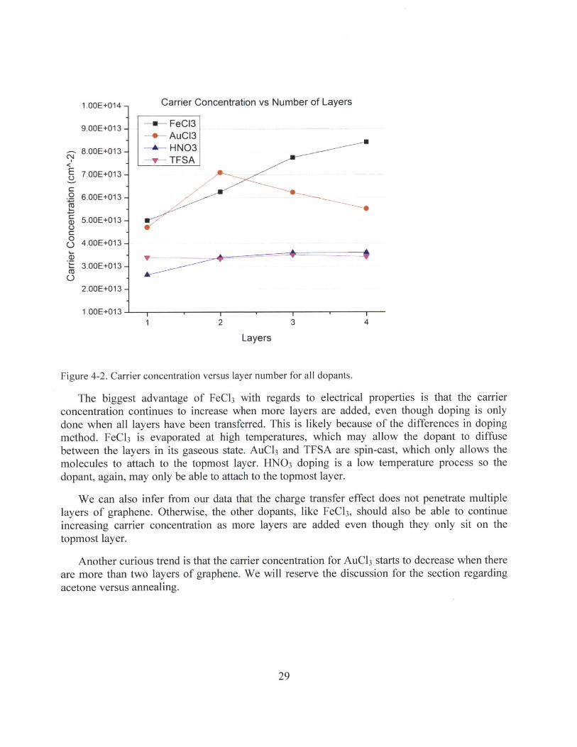
Figure 4-2. Carrier concentration versus layer number for all dopants.
The biggest advantage of FeCl3 with regards to electrical properties is that the carrierconcentration continues to increase when more layers are added, even though doping is onlydone when all layers have been transferred. This is likely because of the differences in dopingmethod. FeCl 3 is evaporated at high temperatures, which may allow the dopant to diffuse
between the layers in its gaseous state. AuCl3 and TFSA are spin-cast, which only allows themolecules to attach to the topmost layer. HNO 3 doping is a low temperature process so thedopant, again, may only be able to attach to the topmost layer.
We can also infer from our data that the charge transfer effect does not penetrate multiplelayers of graphene. Otherwise, the other dopants, like FeCl 3, should also be able to continue
increasing carrier concentration as more layers are added even though they only sit on thetopmost layer.
Another curious trend is that the carrier concentration for AuCl3 starts to decrease when thereare more than two layers of graphene. We will reserve the discussion for the section regarding
acetone versus annealing.
29
1.00E+014 ,

4.2.2 Stability in Atmosphere
We compare the sheet resistance and carrier concentration over time for the various dopants.TFSA is reported to be air-stable while AuCl 3 and HN0 3 have been shown to be unstable in air.The data is shown below.
220- Absolute Sheet Resistance Over Time
* FeCI3 , A
200 * AuCI3& HNO3v TFSA
180
V C 160
X 140-
U) 120-
100-
80-110 100
Time (h)
Figure 4-3. Absolute sheet resistance for all dopants over time.
Relative Sheet Resistance Over Time
2.2 FeC3AuCI3
2.0 HNO3TFSA
cc 1.8-
M 1.6
0
1.0 -
0.8.,,,1 10 100
Time (h)
Figure 4-4. Relative sheet resistance for all dopants over time (normalized to initial value).
30

Relative Carrier Concentration Over Time
9T
FeC13AuCl3
1.2 -
10-
0.8-
0.4 -
0.2-
HNO3TF-SA
1 10
*e W.
.10100
Time (h)
Figure 4-5. Absolute carrier concentration for all dopants over time.
Absolute Carrier Concentration Over Time
FeC3AuCI3HNO3TFSA
\og
VA--AI
13 1 . . .-. . . .. . . . . . .10
Time (h)
100
Figure 4-6. Relative carrier concentration for all dopants over time (normalized to initial value).
31
C
0
0Q)
2)
Q:
-
5.50E+013 -
5OOE+013 -
4.50E+013 -
0 4.00E+013 -
.3.50E+013 -
0 3.00E+013 -U
'C
U
2.50E+013 -
200E+013-
1,50E+013 -
1.00E+01

In terms of sheet resistance over time, FeCl 3 is superior to AuCl3 in air stability but inferiorto TFSA and HN0 3. For all dopants, the carrier concentration decreases sharply over the courseof 1 week, eventually settling to roughly 1.5x10 3 Cm-2 after two weeks. The more heavily dopedsamples (FeCl 3, AuCl 3) exhibit larger drops than the lighter doped ones (HNO 3). TFSA is aninteresting case because even though the carrier concentration drops significantly, the sheetresistance only increases by -20% because the mobility recovers over time. This would suggestthat TFSA damages the samples less than the other dopants. It has been reported that TFSA iscompletely stable in air for more than 2 weeks but our experiments seem to indicate otherwise2 5 .This could be because of different ambient conditions. Nonetheless, TFSA still appears to havethe best air stability of all the dopants we discuss. HN0 3 also appears to have reasonably goodair stability in spite of other reports in literature but this could be due to the worse starting value.We do note, however, that spin-casting a 300nm layer of PMMA on FeCl3 prevents theconductivity from degrading over time. This is not possible for TFSA because it dissolves inAnisole.
As before, we compare the time evolution of sheet resistance at 130*C over 120min. Again,the samples are left in air for 24h to separate the effects of initial increase in resistance with timeand with temperature.
Sheet Resistance at 130C Over Time
1.5 FeCl3-- AuCl3
CD 1.4- HNO3U TFSA~
1.3--
1.2 -
1.0-
0 20 40 60 80 100 120
Time (min)
Figure 4-7. Time evolution of sheet resistance for all dopants at 130C.
It would appear that FeCl3 and AuCl 3 are quite stable at 130'C but HNO 3 and TFSA are not;this is most likely due to the different physical properties of the dopants. Both HN0 3 and TFSAare quite volatile at room temperature so it is likely that they would degas quickly at 130"C.FeCl3 and AuCl3 are stable powders at room temperatures and have relatively high boiling pointsso they would be less prone to evaporation at higher temperatures.
32

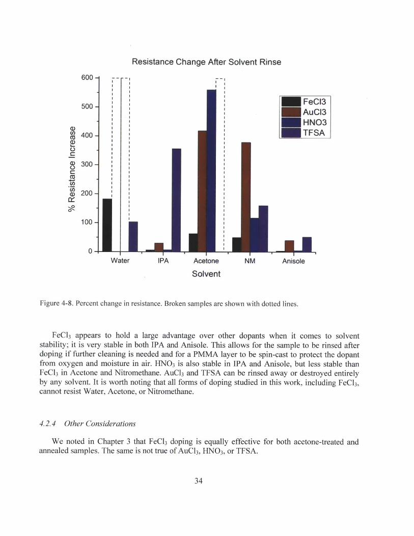
4.2.3 Stability in Solvents
We compare the relative solvent stability of the dopants by immersing for 2min. We use thepercentage change in resistance as the primary metric to account for the different starting points.
Table 4-2. Percentage increase in sheet resistance.
FeCl3 AuCl 3 HNo3 TFSAWaterIPAAcetone 6Nitromethane bAnisole 05
this at Change (10he%)
Mdeate Change (1000)
M Large Change (>100%o)Sample Discontinuous
bold Sample Damaged
In two cases, FeCl3 in water and AuCl3 in Anisole (bolded in Table 4-2), the increase in sheetresistance is substantially larger than the change in carrier concentration. Thus, we can attributethis to degraded mobility, which suggests that the sample was damaged. In other cases, thedamage was severe enough that the sample was no longer continuous over a large area and thusdid not have measurable sheet resistance. The results are summarized in Figure 4-8.
Table 4-3. Percentage change in carrier concentration.
FeCl3 AuCla HNO3 TFSAWaterIPA41AcetoneNitromethane-4'Anisole-2
33
Resistance Change After Solvent Rinse
Water IPA
600
500
400
300
200
100
0
-- I
Acetone
Solvent
-FeC13AuCI3
-HNO3-TFSA
Anisole
Figure 4-8. Percent change in resistance. Broken samples are shown with dotted lines.
FeCl3 appears to hold a large advantage over other dopants when it comes to solventstability; it is very stable in both IPA and Anisole. This allows for the sample to be rinsed afterdoping if further cleaning is needed and for a PMMA layer to be spin-cast to protect the dopantfrom oxygen and moisture in air. HN0 3 is also stable in IPA and Anisole, but less stable thanFeCl 3 in Acetone and Nitromethane. AuCl 3 and TFSA can be rinsed away or destroyed entirelyby any solvent. It is worth noting that all forms of doping studied in this work, including FeCl3,cannot resist Water, Acetone, or Nitromethane.
4.2.4 Other Considerations
We noted in Chapter 3 that FeCl3 doping is equally effective for both acetone-treated andannealed samples. The same is not true of AuCl3, HNO 3, or TFSA.
34
a)co
CU
0
0)
NM
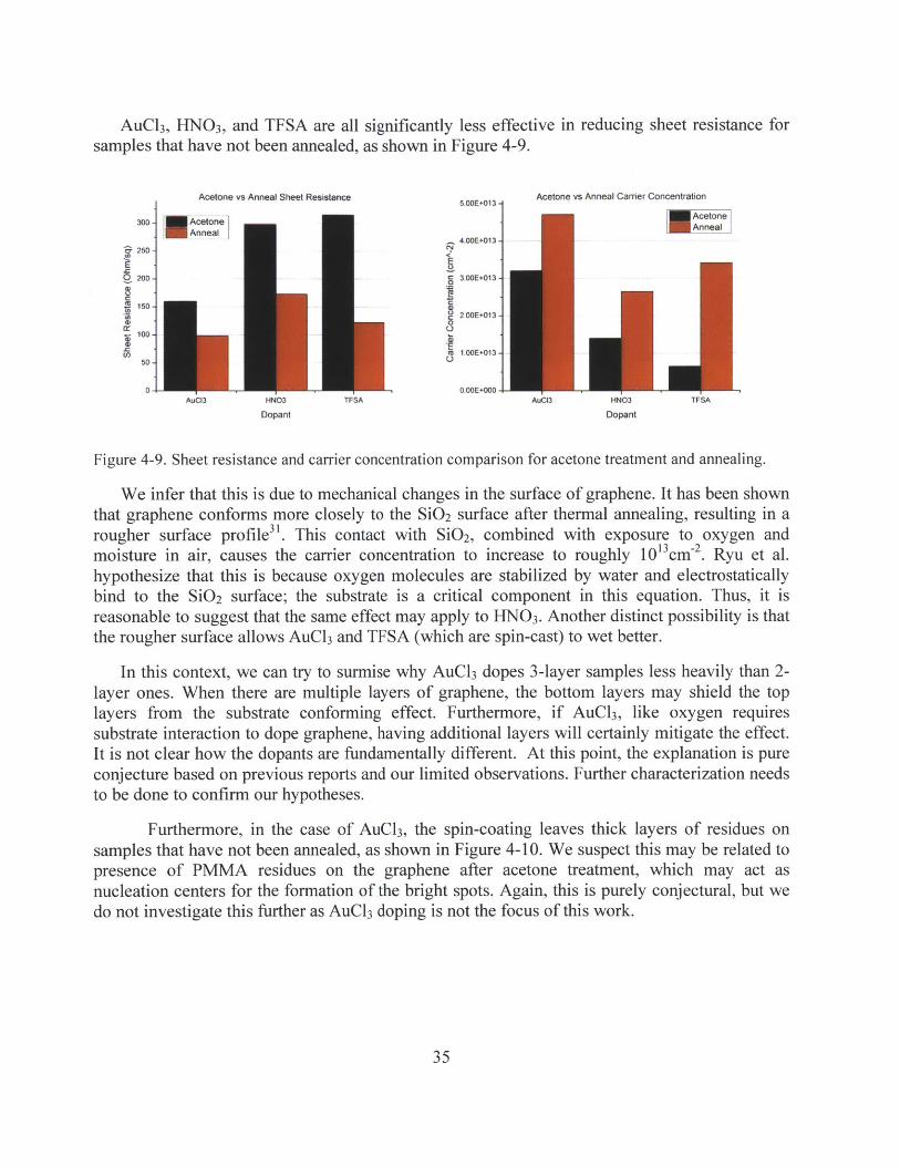
AuCl3, HN0 3, and TFSA are all significantly less effective in reducing sheet resistance forsamples that have not been annealed, as shown in Figure 4-9.
Acetone vs Anneal Sheet Resistance Acetone vs Anneal Carrier Concentration
300 Acetone Anne- Anneall4.OOE+013 -
250
S200 3.OOE+013
0 2.00E+013 -50
100-
50 U.0 1.00E+013
0 AuCI3 HNO3 TFSA O.E'000 Au1 3 HNO3 TFSADopant Dopant
Figure 4-9. Sheet resistance and carrier concentration comparison for acetone treatment and annealing.
We infer that this is due to mechanical changes in the surface of graphene. It has been shownthat graphene conforms more closely to the SiO 2 surface after thermal annealing, resulting in arougher surface profile3 1. This contact with SiO2, combined with exposure to oxygen andmoisture in air, causes the carrier concentration to increase to roughly 10 3 cm 2 . Ryu et al.hypothesize that this is because oxygen molecules are stabilized by water and electrostaticallybind to the SiO 2 surface; the substrate is a critical component in this equation. Thus, it isreasonable to suggest that the same effect may apply to HNO 3. Another distinct possibility is thatthe rougher surface allows AuCl 3 and TFSA (which are spin-cast) to wet better.
In this context, we can try to surmise why AuCl3 dopes 3-layer samples less heavily than 2-layer ones. When there are multiple layers of graphene, the bottom layers may shield the toplayers from the substrate conforming effect. Furthermore, if AuCl3, like oxygen requiressubstrate interaction to dope graphene, having additional layers will certainly mitigate the effect.It is not clear how the dopants are fundamentally different. At this point, the explanation is pureconjecture based on previous reports and our limited observations. Further characterization needsto be done to confirm our hypotheses.
Furthermore, in the case of AuCl3, the spin-coating leaves thick layers of residues onsamples that have not been annealed, as shown in Figure 4-10. We suspect this may be related topresence of PMMA residues on the graphene after acetone treatment, which may act asnucleation centers for the formation of the bright spots. Again, this is purely conjectural, but wedo not investigate this further as AuCl3 doping is not the focus of this work.
35

Figure 4-10. Optical images of AuCl 3 doped graphene. a) Annealed sample. b) Acetone-treated sample.The bright particles present on the acetone-treated graphene cause the surface of the graphene to appeardull by eye.
Another important consideration is the speed and cost of doping. This is one aspect in whichFeC13 is markedly inferior to its competitors. AuCl3 and TFSA only require a spin coater andHNO 3 only requires a petri dish whereas FeC13 requires a furnace, sealable chamber, and gasflow. Although the actual doping time is short, the overhead time is quite long, as the furnacetakes time to heat and the chamber must be washed after several cycles. Scaling is possible, butmay be expensive, as the chamber and furnace must encapsulate all samples. Thus, only incertain situations would the advantages of FeCl3 merit the increase in cost and complexity.
36

Chapter 5
5 Summary and Conclusions
In summary, we have investigated and characterized the doping of CVD graphene usingIron(III) Chloride . We were able to demonstrate that FeCl 3 can dope graphene to sheetresistances as low as 720hm, which is the best value reported in literature thus far.
Ultimately, the purpose of doping is to increase the carrier concentration, thereby shifting theFermi level and reducing sheet resistance. All four dopants studied in this work - FeCl3, AuCl 3,HN0 3, and TFSA - do this sufficiently well. The difference in sheet resistance achievable byFeCl 3 compared to the other dopants is, at first glance, minor and irrelevant, as it is difficult toimagine a device that would work with 95Ohm graphene but would not work with 1200hmgraphene. However, if in the future graphene becomes relevant in industry, performanceimprovements of 10-20% as a result of higher conductivity would be tremendous.
In terms of relevance to research applications, the main advantage of FeCl3-doped grapheneis not achieving lower sheet resistance, but rather, better compatibility with other processes. Thekey positive points of FeCl3 doping, not necessarily relative to other dopants, can be summarizedas follows:
1) All dopants experience diminishing returns with regard to conductivity as the number ofgraphene layers is increased, but it is not as severe in the case of FeCl3 (and AuCl 3).
2) It is stable in some solvents such as IPA and Anisole likely owing to its inorganic nature.This allows a layer of PMMA to be used as a protective coating to prevent degradationover time.
3) It is equally effective for acetone-treated and annealed samples.4) The doping process is scalable.
However, the negative points are:
1) The doping process is more involved and more difficult to control.2) The doping process requires high temperatures, albeit for a short period of time, making
it impractical for some substrates.3) Like other dopants, it is not stable in air.4) Rinsing with water after doping causes the graphene to break.
At the very least, FeCl 3 doping is a viable alternative to AuCl3 or HN0 3 and may be superiorfor some purposes. Because circumstances encountered during research can vary greatly, it ishighly advantageous to have a larger repertoire of techniques. Our work thoroughly characterizesthis doping method and provides a foundation for applications in the future.
37

38

References
1. Li, X.; Cai, W.; An, J.; Kim, S.; Nah, J.; Yang, D.; Piner, R.; Velamakanni, A.; Jung, I.;Tutuc, E.; Banerjee, S. K.; Colombo, L.; Ruoff, R. S. Science 2009, 324, (5932), 1312-4.2. Park, H.; Brown, P. R.; Bulovid, V.; Kong, J. Nano Letters 2011, 12, (1), 133-140.3. Park, H.; Howden, R. M.; Barr, M. C.; Bulovid, V.; Gleason, K.; Kong, J. ACS Nano 2012, 6,(7), 6370-6377.4. Kasry, A.; Kuroda, M. A.; Martyna, G. J.; Tulevski, G. S.; Bol, A. A. ACS Nano 2010, 4, (7),3839-3844.5. Tianhua, Y.; Liang, C.-W.; Kim, C.; Eui-Sang, S.; Bin, Y. Electron Device Letters, IEEE2011, 32, (8), 1110-1112.6. Bae, S.; Kim, H.; Lee, Y.; Xu, X.; Park, J.-S.; Zheng, Y.; Balakrishnan, J.; Lei, T.; Ri Kim,H.; Song, Y. I.; Kim, Y.-J.; Kim, K. S.; Ozyilmaz, B.; Ahn, J.-H.; Hong, B. H.; Iijima, S. NatNano 2010, 5, (8), 574-578.7. Kim, K. K.; Reina, A.; Shi, Y.; Park, H.; Li, L.-J.; Lee, Y. H.; Kong, J. Nanotechnology2010, 21, (28), 285205.8. Yan, C.; Kim, K.-S.; Lee, S.-K.; Bae, S.-H.; Hong, B. H.; Kim, J.-H.; Lee, H.-J.; Ahn, J.-H.A CS Nano 2011, 6, (3), 2096-2103.9. Ni, G.-X.; Zheng, Y.; Bae, S.; Tan, C. Y.; Kahya, 0.; Wu, J.; Hong, B. H.; Yao, K.;Ozyilmaz, B. A CS Nano 2012, 6, (5), 3935-3942.10. Khrapach, I.; Withers, F.; Bointon, T. H.; Polyushkin, D. K.; Barnes, W. L.; Russo, S.;Craciun, M. F. Advanced Materials 2012, 24, (21), 2844-2849.11. Chen, J.-H.; Jang, C.; Xiao, S.; Ishigami, M.; Fuhrer, M. S. Nat Nano 2008, 3, (4), 206-209.12. Li, X.; Cai, W.; An, J.; Kim, S.; Nah, J.; Yang, D.; Piner, R.; Velamakanni, A.; Jung, I.;Tutuc, E.; Banerjee, S. K.; Colombo, L.; Ruoff, R. S. Science 2009, 324, (5932), 1312-1314.13. Reina, A.; Jia, X.; Ho, J.; Nezich, D.; Son, H.; Bulovic, V.; Dresselhaus, M. S.; Kong*, J.Nano Letters 2009, 9, (8), 3087-3087.14. Cheng, Z. G.; Zhou, Q. Y.; Wang, C. X.; Li, Q. A.; Wang, C.; Fang, Y. Nano Letters 2011,11, (2), 767-771.15. Cheng, Z.; Zhou, Q.; Wang, C.; Li, Q.; Wang, C.; Fang, Y. Nano Letters 2011, 11, (2), 767-771.16. Goossens, A. M.; Calado, V. E.; Barreiro, A.; Watanabe, K.; Taniguchi, T.; Vandersypen, L.M. K. Appl Phys Lett 2012, 100, (7).17. Lindvall, N.; Kalabukhov, A.; Yurgens, A. JAppl Phys 2012, 111, (6).18. Suk, J. W.; Lee, W. H.; Lee, J.; Chou, H.; Piner, R. D.; Hao, Y.; Akinwande, D.; Ruoff, R. S.Nano Letters 2013, 13, (4), 1462-1467.19. Hsu, C.-L.; Lin, C.-T.; Huang, J.-H.; Chu, C.-W.; Wei, K.-H.; Li, L.-J. ACS Nano 2012, 6,(6), 5031-5039.20. Petrone, N.; Dean, C. R.; Meric, I.; van der Zande, A. M.; Huang, P. Y.; Wang, L.; Muller,D.; Shepard, K. L.; Hone, J. Nano Letters 2012, 12, (6), 2751-2756.21. Ferrari, A. C.; Meyer, J. C.; Scardaci, V.; Casiraghi, C.; Lazzeri, M.; Mauri, F.; Piscanec, S.;Jiang, D.; Novoselov, K. S.; Roth, S.; Geim, A. K. Phys Rev Lett 2006, 97, (18).22. Kalbac, M.; Reina-Cecco, A.; Farhat, H.; Kong, J.; Kavan, L.; Dresselhaus, M. S. A CS Nano2010, 4, (10), 6055-6063.
39

23. Das, A.; Pisana, S.; Chakraborty, B.; Piscanec, S.; Saha, S. K.; Waghmare, U. V.; Novoselov,K. S.; Krishnamurthy, H. R.; Geim, A. K.; Ferrari, A. C.; Sood, A. K. Nat Nanotechnol 2008, 3,(4),210-215.24. Zhao, W. J.; Tan, P. H.; Liu, J.; Ferrari, A. C. JAm Chem Soc 2011, 133, (15), 5941-5946.25. Tongay, S.; Berke, K.; Lemaitre, M.; Nasrollahi, Z.; Tanner, D. B.; Hebard, A. F.; Appleton,B. R. Nanotechnology 2011, 22, (42).26. Miao, X.; Tongay, S.; Petterson, M. K.; Berke, K.; Rinzler, A. G.; Appleton, B. R.; Hebard,A. F. Nano Letters 2012, 12, (6), 2745-2750.27. Li, X. M.; Xie, D.; Park, H.; Zhu, M.; Zeng, T. H.; Wang, K. L.; Wei, J. Q.; Wu, D. H.;Kong, J.; Zhu, H. W. Nanoscale 2013, 5, (5), 1945-1948.28. Kim, K. K.; Reina, A.; Shi, Y. M.; Park, H.; Li, L. J.; Lee, Y. H.; Kong, J. Nanotechnology2010, 21, (28).29. Song, J.; Kam, F.-Y.; Png, R.-Q.; Seah, W.-L.; Zhuo, J.-M.; Lim, G.-K.; Ho, P. K. H.; Chua,L.-L. Nat Nano 2013, advance online publication.30. Hsu, C. L.; Lin, C. T.; Huang, J. H.; Chu, C. W.; Wei, K. H.; Li, L. J. A CS Nano 2012, 6, (6),5031-5039.31. Ryu, S.; Liu, L.; Berciaud, S.; Yu, Y. J.; Liu, H. T.; Kim, P.; Flynn, G. W.; Brus, L. E. NanoLetters 2010, 10, (12), 4944-495 1.
40