Embed Size (px)
Citation preview

United States Patent [191 Onyszchuk et a1.
4,745,568 May 17, 1988
[11] Patent Number:
[45] Date of Patent:
[54] COMPUTATIONAL METHOD AND APPARATUS FOR FINITE FIELD MULTIPLICATION
[76] Inventors: Ivan M. Onyszchuk, 62 Dorset St. #5; Ronald C. Mullin, 533 Twin Oaks Cres.; Scott A. Vanstone, 333 Auburn Drive, all of Waterloo, Ontario, Canada
[21] Appl. No.: 739,220
[22] Filed: May 30, 1985
[51] Int. Cl.4 ......................... .. G06F 7/52; G06F 7/ 38 [52] U.S. Cl. ............................ .. 364/754; 364/746 [58] Field of Search .............................. .. 364/754-760,
364/746
[56] References Cited U.S. PATENT DOCUMENTS
4,037,093 7/ 1977 Gregg et a1. ...................... .. 364/754 4,251,875 2/1981 Marver et a1. .. 364/754 4,587,627 5/1986 Omura et al. ..................... .. 364/754
OTHER PUBLICATIONS
C. C. Wang et al., “VLSI Architectures for Computing Multiplications and Inverses in GF (2'"), IEEE Trans.
on Computers, vol. C-34, No. 8, Aug. 1985, pp. 709-717. B. A. Laws, Jr. et al., “A Cellular-Array Multiplier for GF (2"‘)”, IEEE Trans. on Computers, vol. C-ZO, No. 12, Dec. 1971, pp. 1573-1578. K. Z. Pekmestzi et al., “A Two’s Complement Cellular Array Multiplier”, The Radio and Electronic Engineer, vol. 51, No. 2, Feb. 1981, pp. 94-96.
Primary Examiner—Gary V. Harkcom Assistant Examiner—Long Thanh Ngyuen Attorney, Agent, or Firm-Fleit, Jacobson, Cohn & Price
[57] ABSTRACT A multiplier for obtaining the product of two elements in the ?eld GF(2’") utilises the normal basis representa tion of each element. The product is also represented in normal basis form with each binary digit of the bit vec tor being determined by a sum of the product of the binary digits representing the two elements. By group ing like ones of one of the binary digits in the expression for the binary digit of the product and offsetting the suffixes of the binary digits, it is possible to accumulate grouped terms of each of the binary digits of the prod uct simultaneously.
27 Claims, 5 Drawing Sheets
I" _ — — _ _ _ _ — — _ _ _ _ _ — — _ — — — _ _ _ "' _I
g >6 ‘P 1. I . ¢o+¢1+c2+c3+¢L p ; |
C C C " l C; 0 ac‘ 2 o L i
| ‘l8 18 | | - l /20 l
CLOCK>| I | d’ m’ d‘ I
I I I
10 I 16\~ b 0- b -. b2 .- b3 -> b; 12 l O - l _ _ -
Ed] I I I I 20 ' I I l I l
l : d0 _” "'" cl2 l
I I I l
g > > .1 I I 36 18 1e 18 |
l I 1 C2 C4 C0 C0 C2 | C3 L _ _ _ _ _ _ _ _ _ _ _ _ _ _ _ _ . _ _ _ _ _.._.l

US. Patent May 17,1988 Sheet 1 0f 5 4,745,568
_| l I I I l I I I I I I l I I I l I I I l I I II II_ I.‘ u S 8 d 8 .6 8 NO _ P w
_
_ WWI? \UW/ "
n 9 Q 2 @m _
a ~
_ _ M M _ _
_ Nu I.l € III on n
_
_ \ I _
ON
_ _
_ qn Al-l m2 ‘I ND ‘I. _.D ‘I .
_ Q\ ,/Q _ _ : ~ _
_ _
_ € Ill 2. u _ 8\ m . _ A V630
_ 2 mm _
_ <0 . mu w _
_ Q G 08 cu Nu _
_ _
_ v0 ‘I no ‘.I NU ‘i. J ‘I 00 _ _ .>\ N ~_ "
r I | l I I I I I I I I I l I I Iel I I m... I I I L


4,745,568 1
COMPUTATIONAL METHOD AND APPARATUS FOR FINITE FIELD MULTIPLICATION
BACKGROUND OF THE INVENTION
1. Field of the ‘Invention The present invention relates to a method and appara
tus for multiplying two elements in the ?nite ?eld GF(Z'").
2. Description of the Related Art As explained fully in European application No.
0080528 from which the following discussion is taken, the ?nite ?eld GF(Z'") is a number system containing 2'" elements. Its attractiveness in practical applications results from the ability to represent each element by a vector of in binary digits. The practical application of error-correcting codes makes considerable use of com putation in GF(Z’"). Both the encoding and decoding devices for the important Reed-Solomon codes must perform computations in GF(Z'"). The decoding device for the binary Bose-Chaudhuri-Hocquenghem codes also must perform computation in GF(Z'"). The reader is referred to “Error-Correcting Codes” by W. W. Pe terson and E. J . Weldon, Jr., 2nd Ed., the MIT. Press, 1972, for details of these and other applications of GF(2'") computation for error-correction. There exist cryptographic systems with encryption
and decryption algorithms that require exponentiation operations on large numbers. Several public-key cryp tosystems have been proposed that require or may be adapted to use the exponentiation of elements in GF(Z'"). Since the process of exponentiation consists of squaring and multiplication operations, it is essential that these operations be performed as quickly and ef? ciently as possible. The reader is referred to “Cryptog raphy and Data Security” by D. E. Denning, Addison Wesley, 1983, for desriptions of GF(Z'") arithmetic and exponentiation algorithms, and for examples of public key cryptosystems utilizing these algorithms. Recent advances in the art of secrecy coding also require the use of computation in GF(2'"). The reader is referred to the letter “Implementing Public Key Scheme”, by S. Berkovits, J. Kowalchuk and B. Schanning, IEEE Communications Magazine, Vol. 17, pp. 2-3, May 1979. The ?nite ?eld GF(2) is the number system in which
the only elements are the binary numbers 0 and 1 and in which the rules of addition and multiplication are the following:
These rules are commonly called modulo-two arithme tic. Hence all additions speci?ed in logic expressions or by adders in this application are performed modulo two. In addition, multiplication is implemented with logical AND gates to correspond with the rule set out at (1) above. The ?nite ?eld GF(Z'"), where m is an integer greater than 1, is the number system in which there are 2'" elements and in which the rules of addition and multiplication correspond to arithmetic modulo an irre ducible polynomial of degree in with coef?cients in GF(Z). Although in an abstract sense there is for each In only one ?eld GF(2'"), the complexity of the logic cir
5
15
20
25
30
35
45
55
60
65
2 cuitry required to perform operations in GF(Z’") de pends strongly on the particular way in which the ?eld elements are represented. The conventional approach to the design of logic
circuitry to perform operations in GF(Z'") is described in such papers as T. Bartee and D. Schneider, “Compu tation with Finite Fields”, Information and Control, Vol. 6, pp. 79-98, 1963. In this conventional approach, one ?rst chooses a polynomial P(X) of degree m which is irreducible over GF(2), that is P(X) has binary coef? cients but cannot be factored into a product of polyno mials with binary coef?cients each of whose degree is less than m. An element A in GF(Z'") is then de?ned to be a root of P(X), that is, to satisfy P(A)=0. The fact that P(X) is irreducible guarantees that the m elements A°= 1, A, A2, . . . , A'"—1 of GF(Z'") are linearly inde pendent over GF(2), that is, that bQ+biA+b2A2+ . . . +bm_1A'" -1 vanishes only when the binary digits b0,b1,b2 . . . , bm_1 are all zeroes. The conventional
approach is then to assign the unit vectors of length m with binary components to the elements, 1, A, A2, . . . , A'"—1. As a speci?c example of the conventional approach,
consider the ?nite ?eld GF(23) with the choice
P(X)=X3+X+l (2)
for the irreducible polynomial of degree 3. The next step is to de?ne A as an element of GF(23) such that
The following assignment of unit vectors is then made:
A°=1=[0, 0, 1]
A=[O, 1, 0]
A2=[1, o, 0] (4)
An arbitrary element B of GF(23) is now represented by the binary vector [b2, b1, b()] with the meaning that
B=[bab1,b0]=b2A2+b1A+bo (5)
Let C=[c2,c1,c0] be a second element of GF(23). It follows from equations (4) and (5) that
B-i-c=lbz+vtbi+vbbo+col- (6)
Thus, in the conventional approach, addition in GF(2'") is easily performed by logic circuitry that merely forms the modulo-two sum of the two vectors representing the elements to be summed component-by~component. Multiplication is, however, considerably more complex to implement. Continuing the example, one sees from equation (3) that
where use has been made of the fact that — l = +1 in GF(Z). From the equations (4), (5) and (7) it follows that
B><C=[d7, d1, do] (3)
where

4,745,568 3
Complex logic circuitry is required to implement equa tions (9). Upon taking C=B equation (8), it follows from equation (9) that
where
c0 = b0
ei=b2 (11)
and where use has been made of the facts that b2=b and b+b=0 in GF(2). Whereas the squaring rule of equa tions (1 l) is considerably simpler to implement than the multiplication rule of equations (9), it still has the disad vantage that some additions (in the example, only one) must be performed and that the form of the squaring rule varies among the components of the square. By way of summary, one can say that the conven
tional approach to the design of logic circuitry to per form operations in GF(2'") leads to simple circuitry for
" addition, somewhat more complex circuitry for squar _‘ ing, and very complex circuitry for multiplication.
In the European application No. 0080528 noted ‘ above advantage was taken of the following special features of the ?nite ?eld GF(2'"). There always exists a so-called normal basis for this ?nite ?eld, that is, one can always ?nd a ?eld element A such that A, A2, A4, . . . , A2"'-1 are a basis for GF(2'") in the sense that
every ?eld element B can be uniquely written as
where b0, b1, b2, . . . , bm_1 are binary digits. Moreover, squaring in GF(2'") is a linear operation in the sense that for every pair of elements B and C in GF(2'")
(B+C)2=B2+C2 (13)
Further, it is the case for every element B of GF(2'") that
B2m=B (14)
The inventors in the above application sought to simplify the multiplication procedure by initially choos ing a polynomial P(X) of degree m which is irreducible over GF(2) and which has linearly independent roots. This latter condition on P(X) insures that upon de?ning A as an element of GF(2'") such that P(A)=0 then A, A2, A4, . . . A2’"—1 form a normal basis for GF(2'"). For a discussion of normal bases in ?nite ?elds, the
reader is referred to “Finite Fields” by Lidl and Neide reiter. Then ifB=[bm_1, . . . , b2, b1, b0] and C=[cm_1,
. , c2, c1, 00] are any two elements of GF(2'") in said normal basis representation, then the product
15
20
25
35
45
50
55
60
4
D=BXC=[dm_1, . . . , d2, d1, do] (15)
has the property that the same logic circuitry which when applied to the components or binary digits of the vectors representing B and C produces dm_1 will se quentially produce the remaining components d,,,_g, . . . , d2, d1, d0 of the product when applied to the compo nents of the successive rotations of the vectors repre senting B and C.
This may be appreciated by considering the binary digits d2, d1, d0 of e.g. equation (9) above where
Like ones of one of the binary digits b,-or c; are grouped to obtain grouped terms so that these may be rewritten in the form
Where an expression such as b0(c1+c2) is subsequently referred to as a grouped term. Thus the logic equation for d1 could be derived from that for d; by reducing the suf?x of all binary digits b,-, c,-, by 1 (Modulo-3). A prac tical implementation was achieved by entering the vec tors in respective shift registers, establishing connec tions and implementing digital logic circuitry to gener ate all terms of the component d2 simultaneously. Then the shift register contents are rotated one bit position to obtain d1, and, similarly d0. Thus, by rotating the vec tors B and C in the two shift registers, the binary digits of the product vector D could be generated by the one logic circuit. However, whilst the above proposal is more ef?cient
than the conventional approach, it suffers the disadvan tage that all grouped terms constituting one binary digit of the vector must be added simultaneously at one loca tion. This makes the implementation of the logic com plicated, and for large values of m, (e.g. greater than 250), impractical. The above European application also proposes the simultaneous or parallel generation of all in binary digits of the product vector by m identical multiplier logic circuits. However, this simply com pounds the dif?culty of logic implementation because of the increase in external shift register connections and the large amount of circuitry required.
SUMMARY OF THE INVENTION
The applicants have recognised that multiplication may be implemented by storing bit vectors B and C in respective shift registers and establishing connections to respective accumulating cells such that a grouped term of each of the expressions d,- is generated in respective ones of m accumulating cells. By rotating the bit vec tors B and C in the shift registers and by rotating the contents of the accumulating cells each grouped term of a respective binary digit d,~ is accumulated in successive cells. Thus all of the binary digits of the product vector

4,745,568 5
are generated simultaneously in the accumulating cells after one complete rotation of the bit vectors B and C.
BRIEF DESCRIPTION OF THE DRAWINGS
Embodiments of the invention will now be described by way of example only with reference to the accompa nying drawings in which FIG. 1 is a block diagram of a multiplier to implement
multiplication of two elements in the ?eld GF(25). FIG. 2 is a block logic diagram of a component used
in the multiplier of FIG. 1. FIG. 3 is a block diagram of an alternative form of
multiplier to implement multiplication of two elements in the ?eld GF(25). FIG. 4 is a block diagram of a further embodiment of
a multiplier to implement multiplication in the ?eld GF(26). FIG. 5 is a block diagram of the multiplier of FIG. 4
with the connections modi?ed for an optimal implemen tation of a GF(26) multiplier.
DETAILED DESCRIPTION
The principle of operation may best be understood by reference to FIGS. 1 and 2 that represents the logic implementation for multiplying two elements in the ?nite ?eld GF(25). Before referring to the ?gures in detail, it will be useful to consider the form of the prod uct D of two elements B and C. B will be of the form B=(b0, b1, b2, b3, b4) in normal
basis representation and C will be of the form C=(c0, c1, c2, c3, 04) in normal basis representation. The product D will be of the form D=(d0, d1, d1, d3,
d4) in normal basis representation. Each of the bit vec tors d,- will consist of grouped terms of the binary digits representing B and C and for the case where m=5
It will be appreciated from the above that by estab lishing logic connections to generate the ?rst grouped term b4(c4+c3+c1+c0) of do, the ?rst grouped term of the binary digits d4, d3, d2, and d1 will also be generated by these same connections if the bit vectors of B and C are successively rotated one place to the right. The
5
20
30
35
45
50
55
65
6 applicants have recognized that if connections are also established to generate the second grouped term of do after the generation of the ?rst grouped term and the bit vectors have been rotated, the connections will in fact generate the second grouped term of d] prior to rotation of the bit vectors B and C. Thus by establishing connec tions to generate successive group terms of the binary digits do in successive clock cycles, it is possible to accumulate in parallel each of the binary digits of the product vector. This simpli?es implementation of the logic.
Referring therefore to FIG. 1, a multiplier 10 in cludes a pair of shift registers 12, 14 each having m cells 16. Shift registers 12 and 14 are loaded with bit vectors B and C respectively so that each cell 16 contains one of the binary digits b; or of. The shift registers 12, 14 are connected, in a manner
to be described below, to the respective ones of accu mulating cells 18 of a term accumulating register 20. The register 20 will have In cells 18 each of which is con?gured as shown in FIG. 2. Referring to FIG. 2, each cell 18 receives a pair of inputs 22, 24 that originate from the shift registers 12, 14 respectively and an input 26 from the adjacent cell 18 of the register 20. The inputs 22, 24 are connected to inputs of an AND gate 28. The output of gate 28 is added to the input 26 at MOD 2 ADDER 30 whose output is connected to a latch 32. The output of latch 32 forms the input 26 of the next cell 18 and receives a clock signal 34 to store the output of ADDER 30. The nature of inputs 22, 24 is determined by the con
nections implemented between the cells 16 of shift regis ters 12, 14 and the cell 18. The connections are arranged such that one grouped term of the binary digits d,- is generated at the output of AND gate 28. Thus for the binary digits do to d4 shown above, the binary digits b0 to b4 and co to ca, are stored in shift registers 12, 14 respectively as indicated in FIG. 1. A ?rst grouped term of do is to be accumulated in cell 18 indicated as do in FIG. 1, i.e. the output of AND gate 42 will represent the grouped term b0(c4+c3+c2). To implement this, a connection is established from the cell 16 of shift regis ter 12 containing the binary digit be to form input 22. Connections from cells 16 of shift register 14 containing binary digits c4, c3 and c2 are made to ADDER 36 whose output, representing c4+c3+c2, forms the input 24 to AND gate 28. The output of AND gate 28 will thus be b0(c4+c3+c2).
Connections are made between the shift registers 12, 14 and the cell 18 indicated as d! to generate the penulti~ mate grouped term of d1, i.e. the term b2(CQ+C4). Thus cells 16 of shift register 14 containing the binary digits c0 and 04 are connected to adder 38 whose output forms input 24 of the cell 18 designated d1 and cell 16 of shift register 12 containing binary digit b; is connected as the input 22 of cell 18 designated d1 so that the output of AND gate 28 is b2(c0+c4).
Similarly the shift registers 12, 14 are connected to the cell 18 indicated d; to generate the third term of binary digit d2, i.e. b4(co+cz); to the cell 18 indicated d3 to provide the second term of binary digit d3, i.e. b1(c2+cQ+c4+c3); and to the cell 18 indicated d4 to produce the first term of binary digit d4, i.e. b3(¢3+¢2+¢0+¢4)
In general, therefore, the jth cell 18 of accumulating register 20 is connected to the shift registers 12, 14 to produce the jth grouped term of a binary digit d; with

4,745,568 7
the subscripts of binary digits b; and c1 increased by j — 1 using modulo m arithmetic. This adjustment of the sub scripts of the grouped term is called “offsetting” and ensures that each of the m accumulating cells generates one grouped term of each of the binary digits d,- during each of m successive clock cycles. With the connections established the binary digits do
to d5 can be generated as follows. First, the binary digits ho to b5 are loaded into shift
register 12 and the binary digits co to 05 are loaded into shift register 14. These may be loaded in parallel or in series as is most appropriate for the particular shift reg ister utilised. The contents of the latches 32 of the cells 18 of accumulating register 20 are cleared by loading zeroes into each. Upon initiation of the multiplication, the grouped terms corresponding to the connections noted above will be generated at the output of each AND gate 28. Because each of the inputs 26 is zero the outpus of the MOD 2 ADDER 30 in each case will correspond to the output of the AND gate 28. On the ?rst rising edge of the clock signal, the output,
of each ADDER 30 is entered into the corresponding latch 32 to appear as the input of the adjacent cell 18. Thus, latch 32 of cell 18 designated do will contain the term bo(c4+c3+c2), latch 32 of cell 18 designated d1 will contain the term b2(co+c4) etc. The ?rst rising edge of the clock signal causes the simultaneous rota tion one position to the right of the contents of registers
, 12, 14 respectively so that the binary digits band 0; are i transferred to an adjacent cell. Thus, the inputs to cell
18 designated do will now be b4 from shift register 12 and (C1+C2+C3) from the adder 36. The output of
i AND gate 28 of cell 18 designated do will thus be b4(c1+c2+c3). The input 26 of cell 18 (do) will be the contents of latch 32 of cell 18 (d4), i.e. b3(c3+c2+co+c4) and thus the output of the MOD 2 ADDER 30 of cell 18 (do) will be
. this corresponds to two grouped terms of the binary . digit d4 set out above. A careful consideration of the output of each ADDER 30 will show that the sum of
' two grouped terms of each binary digit d; will appear as the input of respective latches 32. On the next rising edge of the clock signal, the out
puts of each ADDER 30 will be entered into respective latches 32 and the binary digits b; and C; rotated in the shift registers 12, 14 respectively. Thus, the contents of the latch of cell 18 (do), namely b4(c1+c2+c3)+b3(c3+c2+co+c4) will be present as input 26 of cell 18 (d1) and the output of AND gate 28 of cell 18 (d1) will be bo(c2+c3), i.e. a third grouped term of the binary digit d4. It will be appreciated that after ?ve clock cycles, the sum of all grouped terms of the binary digit d4 will be stored in the latch of cell 18 designated d3 and similarly the sum of all the grouped terms of binary digits d3 to do will be stored in respec tive ones of cells 18. Thus, the bit vector constituting the normal basis representation of product D is avail able by reading the contents of the accumulating regis ter 20.
It will also be noted the connections from the cells 16 of shift registers 12, and 14 are distributed amongst the cells 18 of accumulating register 20 to reduce the num ber of inputs of any adder.
Whilst the above multiplier constitutes a signi?cant improvement over that described in the European pa tent application No. 0080528, the number of connec tions may be reduced further although the number of
40
45
55
65
8 clock cycles required to generate the binary digits d,- is increased. A multiplier for the ?eld GF(25) is shown in FIG. 3 and is similar to that shown in FIG. 1. Accord ingly the reference numerals used in the description of FIGS. 1 and 2 will be used to identify like components with a pre?x 100 added, i.e. reference numeral 12 will become 112. The arrangement shown in FIG. 3 differs in two important ways, namely the provision for ex changing the contents of shift registers 112 and 114 as indicated by dashed lines 150, 152 and the nature of the connections between the cells 116 and cells 118. It will also be noted that the shift registers 112, 114 are con trolled by a separate clock signal, indicated at clock 1, to the accumulating register 120 whose clock signal is indicated at clock 2. The nature of the connections is established from a
further manipulation of the terms representing the bi nary digits di. Thus considering the binary digit d4 above, this may be written as:
and rearranged as:
bars + lbscz + 11263] + [bsro + 11063] + [bm +
11403] + [11261 + biczl + [11264 + 11462] +
[/1164 + 11461]
It will be observed that the terms within the brackets [ ] possess a symmetry such that if one product term is of the form bjck, the other product term is obtained by interchanging the suf?xes, i.e. bkCj. It has been recog nised that by implementing the logic to produce one product term of each pair, the other product term may be obtained from a simple interchange of the contents of the shift registers and by a repeated circuit operation each of the product terms of each pair may be obtained. Moreover, the offsetting principle still applies so that the terms of each binary digit will be generated in paral lel. The expression for digit d4 is
X Y Z
113C; + bacz + bzvs
+ bsco + boos
+ 11304 + luvs
+ bgcl + [1102
+ 17280 + bovz
+ In“ + 11462
+ 11164 + 11461
The product terms in column Y are then selected and like terms grouped as discussed above with reference to FIG. 1. Thus column Y may be expressed as b3(c2+co+c4)+b2(c1+co+c4)+b1c4. By implement ing the logic to generate these terms in successive cells 118 of accumulating register 120, the terms of column Z ‘ will also be generated after interchange of the shift registers 112, 114 by a second pass through the accumu lating cells. The odd term of column X may be gener ated during one of the two passes through the cells 118 with its generation inhibited during the other pass.

4,745,568 9
It will be noted that the grouped terms of column Y would require 3 inputs to two of the ADDERS whilst only 3 of the accumulating cells 118 are utilised. In order to spread the connections evenly between the cells 118, the expression is modi?ed to select one of each pair of product terms but obtain a different grouping. Thus, in the example above, the third and sixth product terms are selected from column Z rather than Y so that the expression b3(c2+c0)+b4(c3+c2)+b2(c1 +c0)+b1c4 is to be imple mented. This increases the number of cells 118 utilised and reduces the number of connections to some of the ADDERS.
Referring therefore to FIG. 3, the ?nal term b1c4 is implemented in the cell 118 designated do (referred to hereafter as 118 [do]) by connecting cell 116 of shift register 112 containing binary digit b1 and cell 116 of shift register 114 containing binary digit c4 to the AND gate 128. The connections to the second of cells 118 is established from a second term with the suf?xes of the binary digits increased by l, Modulo 5 i.e. b3(c2+c1) and in general the jth cell 118 accumulates a jth term of the expression with suf?xes increased by j—1 (Modulo m). ‘
Connections are also established to implement the odd term b303, of column X in cell 118 designated d4. The connections to d4 are modi?ed to include an AND gate 154 to inhibit the accumulation of the add terms e. g. b3c3. The AND gate 154 is located between the cell 116 designated c3 and ADDER 160 and receives as one input the output of cell 116 and as its other input an inhibit signal 156 derived from the clock signal. When the inhibit signal 156 is logic level 0, the output of AND gate 154 will be zero so that zero will be added by ADDER 130 to the contents of the latch 136 of the previous cell 118 [d3]. With the connections established, the binary digits be
to b4 and co to c4 are loaded in respective cells 116 of shift registers 112, 114. The contents of each cell 118 is cleared so that each latch 132 contains 0 and the inhibit signal 156 is held at logic level 0 to force the output of AND gate 154 to also be zero. The contents of the shift registers 112, 114 and the
cells 118 are then rotated one bit position rightwards by successive clock cycles so that after m clock cycles one of each part of the paired product terms is accumulated in respective cells 118. The generation of the terms is shown in table 1 below.
Thus, it will be seen that the terms in d4 correspond to the rewritten expression for one of each of the pairs of product terms.
After ?ve clock cycles, registers 112, 114 will have undergone a complete rotation so that binary digits b, and C] will be stored in the cells 116 in which they were initially loaded. Now the contents of the shift registers 112 and 114
are exchanged through connections 150, 152. This may be accomplished by shifting the contents of both regis ters 112, 114 for ?ve clock cycles as a serial, circular exchange or alternately could be achieved by parallel connections between cells 116. Serial exchange is shown in FIG. 4 and is easiest to implement for large values of m. During the exchange, clock 1 goes through ?ve cycles while clock 2 is held low to prevent un wanted terms accumulating in register 120. When bi nary digits d,- pass through accumulating cells, both clock signals are identical.
5
25
40
45
50
65
10 After the exchange of binary digits, the inhibit signal
156 is set to logic level 1 so that AND gate 154 passes the input from cell 116 to the input of ADDER 160. The circuit operation then continues as exempli?ed by the table below for the next ?ve clock cycles. Again, it will be seen that the terms of each of the binary digits d; are accumulated in each of the cells 118 in parallel so that after 2m clock cycles of computation the binary digits of D are available in the cells 118 of accumulating register 120. Because of the need to exchange the con tents of the shift registers 112, 114, additional clock cycles are required to complete the computation. How ever, the number of the connections between the shift registers and the accumulating register in the multiplier of FIG. 3 is less than those shown in the multiplier of FIG. 1 to compensate for this. The implementation shown in FIG. 3 has been used
to illustrate the generality of the above principle. How ever, in practical implementations particularly for large values of m, the connections may be simpli?ed further by selecting the grouped terms in ascending order of the coef?cient b,- or c,-. In this manner a maximum of two connections between each cell of one of the shift regis ters and the accumulating register is obtained.
In order to reduce the time taken to compute the binary digits d,, the multiplier of FIG. 3 can be further modi?ed as shown in FIG. 4. Again like components will be identi?ed by like reference numerals with a pre?x 2 added for clarity. FIG. 4 shows a multiplier for generating the binary digits d,-in the ?eld GF(26). It will be noted that the shift registers 212 and 214 have been segmented into 3 units, 212a, b, or c and 2140, b or c respectively, each having two cells 116. Similarly, the accumulating register 220 is segmented into 3 units 220a, b or c each having two cells. It will be noted that each of the shift register units 212a, b, and c is connected to a corresponding shift register unit 214a, b and c by paths 2500, b, c, and 2520, b, c respectively. The paths 250,252 are utilised to exchange the contents of the registers 212, 214 between units a, b and c rather than through the entire shift register. In this way the number of clock cycles necessary to transfer the contents of the shift register is reduced from m to the number of cells 216 in each unit. The binary digit d5 of product D in GF(26) is given
by
Thus by implementing the expression b0(¢3 + Cs) +b1c2 + b2(¢0+ Cs)+b3¢1+b4c2 +bs(c4+ C5) the binary digits d; of the normal basis representation of the product D can be generated. It is believed to be apparent from the above discussion that the initial con nections to be established are as follows:
cell 118 physical connection
do b0(¢3 + (:5) d1 bzcs d2 b4(C2 + 61) d3 bow.

4,745,568 11
-continued cell 118 physical connection
In this case, the odd term is generated initially in cell 218 [d5] and the input to the adder 236 associated with cell 218 [d5] that is initially from the cell 216 containing digit c4 is inhibited after the ?rst pass through the accu mulating register 220 by use of an AND gate in a man ner similar to that shown in FIG. 3. The operation of the multiplier of FIG. 4 is similar to
that described above with reference to FIG. 3. How ever, exchange of the contents of the registers 212, 214 occurs over the lines 250, 252 to reduce from 6 to 2 the number of clock cycles necessary to complete the ex change.
It is believed the above examples clearly and explic itly explain the operation of GF(2'") the multiplier. Relatively small values of m have been selected for the sake of simplicity but it will be apparent that the above principles apply for large values of m usually employed in encryption. However, for the larger values of m usually utilised in
encryption, the number of product terms in the expres sion for binary digit d,- may increase quadratically with the value of m. This renders the implementation of a multiplier impractical because of the large number of connections necessary. For those values of m listed in Table 3 there does exist an optimal normal basis in the sense that it yields an expression di that has 2m-l prod
" uct terms, the smallest number possible. Each of the integers m has an indication of type for use in the com puter program discussed below. The binary digits be; of the binary digit do of the product vector D for the opti mal normal basis of a value of m listed in Table 3 may be obtained executing the computer program listed in ap pendix 1. By running the program for m=6 the follow ing results were obtained:
20
25
12
vars do
FIG. 5 shows the implementation of this expression for the segmented GF(26) multiplier shown in FIG. 4 with appropriate modi?cations to the connections to implement the above. The rearrangement of do to obtain these connections will be apparent from the above and consideration of FIG. 5. An optimal multiplier design exists for every value of
m listed in Table 3 such that every accumulating cell 218 has a single input from same shift register cell 216. Thus, m modulo-two ADDERS are eliminated as com pared to the multipliers of FIGS. 1, 3 and 4 further simplifying the circuitry.
In addition, the applicants believe that the maximum number of connections to the output of any shift register cell 216 is three. The above description has utilised block diagram
representations of the registers 12, 14, 20 and the adders and logic functions. However, it is believed that the selection and operation of the components to perform the functions discussed above will be apparent to a person skilled in the art of digital logic design and that further particularisation of the components is not neces sary.

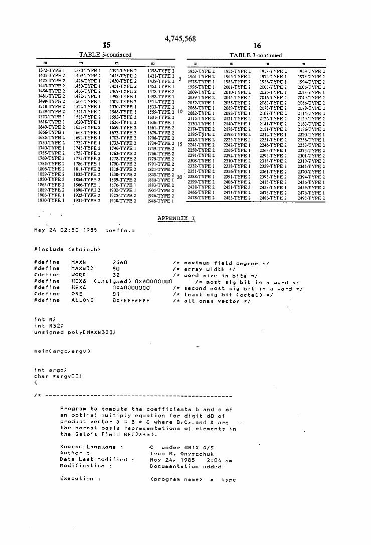
4,745,568 15 16
TABLE 3-continued TABLE 3-con1inued m m m m m m m m
l372-TYPE 1 USO-TYPE 1 l394-TYPE 2 1398-TYPE 2 1953_TYPE 2 1955-TYPE 2 l9S8-TYPE 2 l959-TYPE 2 MOI-TYPE 2 1409-TYPE 2 MKS-TYPE 2 l421-TYPE 2 5 196l-TYPE 2 l965-TYPE 2 l972-TYPE 1 l973-TYPE 2 1425-TYPE 2 l426-TYPE 1 l430-TYPE 2 l439-TYPE 2 l978-TYPE 1 l983-TYPE 2 1986-TYPE 1 l994-TYPE 2 1443-TYPE 2 l450-TYPE 1 1451-TYPE 2 1452-TYPE 1 1996-TYPE 1 2001-TYPE 2 zoos-TYPE 2 2006-TYPE 2 l454-TYPE 2 l463-TYPE 2 l469-TYPE 2 1478-TYPE 2 z009.TYPE 2 2010mm}: 2 2026-TYPE 1 2028-TYPE 1 1481-TYPE 2 l482-TYPE 1 1492-TYPE 1 l498-TYPE 1 2032mm; 2 2045-TYPE 2 2046-TYPE 2 2049-TYPE 2 l499-TYPE 2 ISOS-TYPE 2 l509-TYPE 2 151l-TYPE 2 2052mm; 1 2055mm; 2 2063-TYPE 2 2066-TYPE z ism-TYPE 2 ISZZ-TYPE 1 HBO-TYPE 1 1533-TYPE 2 2068-TYPE 1 2069-TYPE 2 2078-TYPE 2 2079-TYPE 2 1539-TYPE 2 1541-TYPE 2 1548-TYPE 1 l559-TYPE 2 1° ZOSZ-TYPE 1 2098-TYPE 1 2109-TYPE 2 2ll4-TYPE 2 1570-TYPE 1 1583-TYPE 2 1593-TYPE 2 l601-TYPE 2 21 IS-TYPE 2 ZIZI-TYPE 2 2l26-TYPE 2 2l29-TYPE 2 l618-TYPE 1 16Z0-TYPE I 16Z6-TYPE 2 1636-TYPE 1 2l30-TYPE 1 2140~TYPE 1 2l41-TYPE 2 2l63-TYPE 2 1649-TYPE 2 1653-TYPE 2 I659-TYPE 2 1661-TYPE 2 2l74-TYPE 2 2l78-TYPE 2 2181-TYPE 2 2l86-TYPE 2 1666-TYPE 1 1668-TYPE 1 1673-TYPE 2 1679-TYPE 2 2l95-TYPE 2 2l98-TYPE 2 22l2-TYPE 1 ZZZO-TYPE 1 1685-TYPE 2 l692-TYPE 1 17°3-TYPE 2 17°6-TYPE 2 2223-TYPE 2 2225-TYPE 2 223l~TYPE 2 2236-TYPE 1 I'm-TYPE 2 1732-TYPE 1 1733-TYPE 2 1734-TYPE 2 15 224l-TYPE 2 2242-TYPE 1 2246-TYPE 2 2253-TYPE 2 l74o-TYPE 1 1745-TYPE 2 1746-TYPE 1 1749-TYPE 2 2258-TYPE 2 2266-TYPE 1 2268-TYPE 1 2273-TYPE 2 1755-TYPE 2 1758-TYPE 2 1763-TYPE 2 1766'TYPE 2 229l-TYPE 2 2292-TYPE 1 2295-TYPE 2 2301-TYPE 2 1769-TYPE 2 1773-TYPE 2 Ins-TYPE 2 1779'TYPE 2 BOB-TYPE 1 2310-TYPE 2 23l8-TYPE 2 23l9-TYPE 2 "gs-TYPE 2 1786-TYPE 1 I79O-TYPE 2 1791-TYPE 2 2332-TYPE 1 2338-TYPE 1 2339-TYPE 2 2345-TYPE 2 l806-TYPE 2 1811-TYPE 2 1818-TYPE 2 l82l-TYPE 2 2351_TYPE 2 2356_TYPE l 2361;1-YpE 2 Z370_TYPE 1 1829-TYPE 2 1835'TYPE 2 1838-TYPE 2 1845'TYPE 2 20 ‘ BBB-TYPE 1 239l-TYPE 2 2393-TYPE 2 2394-TYPE 2 135°-TYPE 2 1854'TYPE 2 1859-TYPE 2 136°‘TYPE 1 2399-TYPE 2 2406-TYPE 2 24l5-TYPE 2 2436-TYPE 1 1863-TYPE 2 1366‘TYPE 1 ‘Sn-TYPE 1 1883-TYPE 2 2438-TYPE 2 2451-TYPE 2 2458-TYPE 1 2459-TYPE 2 1889-TYPE 2 1398-TYPE 2 WOO-TYPE 1 19°1-TYPE 2 2466-TYPE 1 247l-TYPE 2 2475-TYPE 2 2476-TYPE 1 19°6-TYPE 1 1923-TYPE 2 1925-TYPE 2 1926'TYPE 2 2478-TYPE 2 2483-TYPE 2 2486-TYPE 2 2493-TYPE 2 1930-TYPE 1 I9_3l-TYPE 2 1938-TYPE 2 1948-TYPE 1
' ‘ APPENDIX I
New 2k 02:50 1985 coef fs .c
I! i no Lude (stdio. h>
ldefine M'AXN 2560 /* maximum f i eLd degree */ Sdef ine MAXN32 80 /* array uidth */ ?define WORD 32 /* word size in bi ta */ #define HEXB (unsigned) 0x80000000 /* most a i g bi t in a uord */ Idef ine HEXL 0X40000000 /* second most sig bi t in a word */ ddefine ONE 01 1* least sig bi t (octaL ) */ ?def i ne ALLONE OXFFFFFFFF /* eLL ones vector */
int N; int N32; unsigned poLyEMAXNISZJ?
mainC argciargv )
int argc;
Program to compute the coeff i cients b and c of an optimal muLtipLy equation for digi t d0 of product vector 0 = and D are the norrnaL basis representations of e Lements in the Galois Field GFC 2**m ).
Source Language : Author :
Date Last Modi f i ed : Modi f i cation :
Execution
-C under [van M“ May 21w
(progrém
UNIX O/S Onyszchuk 1985
name) 111
2:04 am Documentation added
type

un
un
un
un
in in un
re
re
re
re
in re
re
re
un
un
un
un
4,745,568 17 18
Resu L t : d0 mu L t'ipLy equation’ 2m-1 pai rs of coefficients b and c . IF an invaL id
i s entered, i s printed.
va Lue of n or type
error message
an
------------------------------------------------- -- */
variable decLarJat i on: */
a i gned *BPCMAXN J; signed *DPCMAXN J; signed *BICMAXN J; signed mask; t terms’ out, out‘l, b; t type; signed *suap; gi ster int i; gi ster int j; gister int k; gi ster int L,‘ 'c t1, t2; gi ster unsigned *bp, **b1r *"XbZ; gister unsigned *dpr *b3! *b4; gister unsigned temp, temp2; signed beta1EMAXN32]; signed betaZEMAXNSZJ; signed oneEMAXN32]; signed tuolZMAXN32];
Read in ve Lue of m and type */ ‘
N = atoi ( argvE 1 J ); type = atoi ( argvEZ] ); -v N32 = (N - 1 ) / WORD + 1;
for ( i = 0; i <= N32; i++ ) poLyC i J = one[ i J = tuoE i 3 = beta1£ i J = 0; ‘
Compute generating poLynom i aL */
i f ( ( type != 1 ) && ( type ! = 2) ) goto next;
1' f ( type == 2 ) {
*tuo = HEXB;
*one = HEX8 l HEXA;
for( i=1; i <N; i++ ) {
*poLy = *two " ( *one >> 1 J;
for ( i=0; j < N32; j++ )
poLyCj ] = twoEj 1 A ( ( oneEj_1 J & ONE ) 7 ConeCj J >>1 I HEXB )
( email)’ I] >> 1 ));
for (i=0; j < N32; j+4:) < twoCj J = oneC j 1; oneCj J = poLyEj J;
> )
}
i f ( type == 1 J <
for ( j = ‘l; j < N32; j ++ ) poLyE j -'I ‘J = ALLONE;
poLyCN32-1 1 OXBOOOOOOO >> C N 7. WORD ); v


4,745,568 23
for (j = N32 ~1;j'> 0; *e =
*e = (*e >> 1) A( feed '2 *poLy }
}
Weclaim: 1. A method of determining the product D of two
elements B and C of the ?nite ?eld GF(2"1), where m is an integer greater than 1, the ?eld having elements A” (0§i<m) that constitute a normal basis, compris
ing the steps of: (a) representing the element B as a vector of binary
digits b,-, where b,- is the coef?cient of A2'' in the nor mal basis representation of B,
(b) representing the element C as a vector of binary digits c;, where c,- is the coef?cient of Ali in the nor mal basis representation of C,
(0) representing the product D of elements B and C as a vector of binary digits d,-, where diis the coef?cient of Ali in the normal basis representation of D, each of said binary digits d,- being expressed in the form of a sum of products of the binary digits D] and ck, (O§j,k<m),
(d) storing in m successive cells of a ?rst recirculating shift register the binary digits, b,-,
(e) storing in m successive cells of a second recirculat~ ing shift register the binary digits, c,-,
(t) selecting at least some of said products of the binary digits bf and ck (0§j,k<m) expressing a binary digit diand grouping like ones of one of the binary digits bj or ck to provide grouped terms of the form
m—l
bi kio mod 2 mod 2
(g) associating each of said grouped terms with a differ ent one of m accumulating cells of an accumulating recirculating shift register,
(h) establishing connections between the cells of said ?rst and second recirculating shift registers and a ?rst of said accumulating cells to provide a ?rst of said grouped terms in said accumulating cell,
(i) establishing connections between the cells of said ?rst and second recirculating shift registers and a second of said accumulating cells adjacent to said ?rst of said accumulating cells to provide an expression equivalent to another of said grouped terms'with the suf?xes of the binary digits of said second grouped term increased by 1 (Modulo m),
(j) repeating step i for successive ones of the grouped terms with the increase in the suf?x of each binary digit of said grouped terms accumulating by 1 (Mod ulo m) for each repetition whereby there is provided in each accumulating cell a grouped term of each of the in binary digits d,,
(k) generating a respective grouped term in at least (m- l) of said accumulating cells,
(1) accumulating modulo 2 each generated grouped term with the previously generated grouped terms accumulated in an adjacent one of said accumulating cells wherein grouped terms of the same binary digit are accumulated in the same cell,
10
25
35
45
55
65
e--)
U);
(m) transferring the contents of each cell of the ?rst and second recirculating shift registers to its next cell, and
v(n) repeating steps k, l and m, (m—l) times whereby after (m—l) repetitions each of said accumulating cells contains the modulo 2 sum of said selected ones of the grouped terms of a different one of the binary digits d,-. 2. A method according to claim 1 comprising the
steps of pairing said products such that one term of each pair has the form bjck and the other of each pair has the form bkcj, and selecting one of each pair together with any product terms that cannot be paired to form said grouped terms.
3. A method according to claim 2 wherein the other product terms of each pair are generated by interchang ing the binary digits of said ?rst and second recirculat ing shift registers upon completion of step It and repeat ing steps k through It.
4. A method according to claim 3 wherein each of said ?rst and second shift recirculating registers are segmented into complementary segments and connec tions are established between said recirculating shift registers such that the contents of one of said segments of one recirculating shift register is interchanged with the contents of the corresponding segment of the other of said recirculating shift registers whereby the contents of the ?rst and second recirculating shift registers are interchanged in less than in clock cycles.
5. A method according to claim 4 wherein the seg ments of each recirculating shift register are of equal size.
6. A method according to claim 3 wherein generation of product terms that cannot be paired is inhibited dur ing one repetition of steps k to n.
7. A method according to claim 1 wherein all of the products are selected for grouping into grouped terms.
8. A method according to claim 1 wherein the estab lishment of connections includes the step of adding summed terms of each grouped term and subsequently multiplying the result thereof by the multiplier bj or ck.
9. A method according to claim 1 including the step of storing the accumulated group terms in a latch.
10. A method of determining the product D of two elements B and C of the ?nite ?eld GF(2"'), where m is an integer greater than 1, the ?eld having elements A” (O_5_i<m) that constitute a normal basis, compris
ing the steps of: (a) representing the element B as a vector of binary
digits b,-, where b; is the coef?cient of A” in the normal basis representation of B,
(b) representing the element C as a vector of binary digits or, where c; is the coef?cient of A2! in the normal basis representation of C,
(0) representing the product D of elements B and C as a vector of binary digits d,-, where d,- is the coef?ci ent of A2’ in the normal basis representation of D, each of said binary digits d,- being expressed in the form of a sum of products of the binary digits bjand ck, (O§j,k<m),
(d) storing in m successive cells of a ?rst recirculating shift register the binary digits, b,-,

4,745,568 25
(e) storing in m successive cells of a second recircu lating shift register the binary digits, 0;,
(t) selecting at least some of said products of a binary digit d,- and grouping like ones of one of the binary digits b]- or ck to provide grouped terms of the form
mod 2 mod 2
(g) establishing connections from respective cells of ' said shift registers to each [+] cell of a recirculat
ing accumulating shift register to produce in each accumulating cell a grouped term of a binary digit representing the vector D, said connections being established such that a ?rst grouped term of one of said binary digits is accumulated in a ?rst of said cells of said accumulating shift register and upon repeated transfer of the contents of said ?rst accu mulating cell through each of said accumulating cells accompanied by successive rotations of said recirculating shift register contents, successive grouped terms of said one binary digit will be gen erated and accumulated in successive accumulating cells,
(h) generating successive ones of said grouped terms of said one binary digit by rotating the vectors representing B and C in the ?rst and second recir culating shift registers,
(i) accumulating modulo 2 said other grouped term with the previously generated grouped terms accu
' mulated in an adjacent one of said accumulating cells to provide grouped terms of said one binary digit, and
(j) repeating the accumulation (m- 1) times whereby grouped terms of each binary digit are accumu lated simultaneously in successive accumulating cells to produce each of the m binary digits of the vector representing the product D simultaneously.
11. A method according to claim 10 wherein all of the products are selected for grouping into grouped terms.
12. A method according to claim 10 comprising the steps of pairing said products such that one term of each pair has the form bjck and the other of each pair has the form bkcj, and selecting one of each pair together with any pairs that cannot be paired to form said grouped terms.
13. A method according to claim 12 wherein the other product terms of each pair are generated by inter changing the binary digits of said ?rst and second recir culating shift registers upon completion of step j and repeating steps h through j.
14. A method according to claim 13 wherein genera tion product terms that cannot be paired is inhibited during one repetition of steps h to j.
15. Apparatus for determining the product of two elements B and C of the ?nite ?eld GF(q'"), where rn is an integer greater than 1, the ?eld having elements
Alli (0§i<m) that constitute a normal basis compris mg:
(a) a ?rst recirculating shift register having m succes sive cells each of which receives a q-ary digit b,- of a vector representing the element B where biis the coef?cient of Aqi in the normal basis representation of B,
LII
25
30
35
45
50
55
60
65
26 (b) a second recirculating shift register having m
successive cells each of which receives a q-ary digit c,- of a vector representing the element C, where c,-is the coef?ci
ent of Aql in the normal basis representation of C, (c) an accumulating recirculating shift register having m successive accumulating cells to accumulate successive grouped terms of each of the q-ary dig its d,- of a vector representing the product D of elements B and C, where d,- is the coef?cient of A4‘ in the normal basis representation of D,
(d) logic means establishing connections from respec tive cells of said recirculating shift registers to each of said accumulating cells to produce in each accu mulating cell a grouped term of a q-ary digit diof a vector representing the product D, said connec~ tions being established such that a ?rst grouped term of one of said q-ary digits is accumulated in a ?rst of said accumulating cells and, upon repeated transfer of the contents of said ?rst accumulating cell through each of said accumulating cells ac companied by successive rotations of said recircu lating shift register contents, successive grouped terms of said one q-ary digit will be generated in successive cells,
(e) said accumulating cell having summing means to sum in GF(q) the output of said logic means and the previously generated grouped terms in an adja cent one of said accumulating cells, and thereby provide a further accumulation of grouped terms,
(f) means to store said further grouped terms, and (g) means to rotate the contents of said recirculating
shift registers through successive cells, whereby after In operations of said summing means each of said store means contains a q-ary digit d,- of the vector representing the product D.
16. Apparatus according to claim 15 wherein said logic means establishes connections to generate grouped terms formed be selecting one of each pair of product terms having the form bjck; bkCj together with any product terms that cannot be paired.
17. Apparatus according to claim 16 including means to interchange the contents of the ?rst and second recir culating shift registers after in successive rotations.
18. Apparatus according to claim 17 including means to inhibit selectively the logic means associated with one of said accumulating cells.
19. Apparatus according to claim 18 wherein said ?rst and second circulating shift registers are segmented and said interchange means is operative to interchange the contents of corresponding segments of said ?rst and second recirculating registers in less than m clock cy cles.
20. Apparatus according to claim 15 wherein said logic means includes adding means to add (modulo q) the contents of respective cells of one of said shift recir culating registers, and
multiplier means to multiply in GF(q) the output of said adding means by the contents of one of the cells of the other of said recirculating shift regis ters.
21. Apparatus according to claim 20 wherein said store means comprises a memory element having an input connected to said summing means and an output