Embed Size (px)
Citation preview

NXP LH7A404_N System-on-Chip datasheet http://www.manuallib.com/nxp/lh7a404-n-system-on-chip-datasheet.html
The advent of 3G technology opens up a wide rangeof multimedia applications in mobile information appliances.The LH7A404 is designed from the ground upwith a 32-bit ARM922 Core to provide high processingperformance, low power consumption, and a high levelof integration. Features include 80 kB on-chip SRAM,fully static design, power management unit, low voltage(1.8 V Core, 3.3 V I/O) and on-chip PLL.satisfy a wide range of requirements and expectations.
ManualLib.com collects and classifies the global productinstrunction manuals to help users access anytime andanywhere, helping users make better use of products.
http://www.manuallib.com

IMPORTANT NOTICE Dear customer, As from June 1st, 2007 NXP Semiconductors has acquired the LH7xxx ARM Microcontrollers from Sharp Microelectronics. The following changes are applicable to the attached data sheet. In data sheets where the previous Sharp or Sharp Corporation references remain, please use the new links as shown below. For www.sharpsma.com use www.nxp.com/microcontrollers for indicated sales addresses use [email protected] (email) The copyright notice at the bottom of each page (or elsewhere in the document, depending on the version) - Copyright © (year) by SHARP Corporation. is replaced with: - © NXP B.V. (year). All rights reserved. If you have any questions related to the data sheet, please contact our nearest sales office via e-mail or phone (details via [email protected]). Thank you for your cooperation and understanding, In addition to that the Annex A (attached hereto) is added to the document. NXP Semiconductors
This Manual:http://www.manuallib.com/nxp/lh7a404-n-system-on-chip-datasheet.html

Product data sheet 1
LH7A404Product data sheet 32-Bit System-on-Chip
FEATURES• 32-bit ARM9TDMI™ RISC Core
– 16 kB Cache: 8 kB Instruction and 8 kB Data Cache– MMU (Windows CE™ Enabled)– Up to 266 MHz; See Table 1 for speed options
• 80 kB On-Chip Static RAM
• Vectored Interrupt Controller
• External Bus Interface– Up to 133 MHz; See Table 1 for bus speed options– Asynchronous and Synchronous interface RAM,
Flash, PC Card and CompactFlash
• Clock and Power Management– 32.768 kHz and 14.7456 MHz Oscillators– Programmable PLL
• Programmable LCD Controller– Up to 1,024 × 768 Resolution– Supports STN, Color STN, AD-TFT, HR-TFT, TFT– Up to 64 K-Colors and 15 Gray Shades
• 9 Channel, 10-bit A/D Converter– Touch Screen Controller– Brownout Detector
• DMA (12 Channels)– External DMA Channels– AC97– MMC– USB
• USB 2.0 Full Speed Host (two downstream ports)
• USB 2.0 Full Speed Device
• Synchronous Serial Port (SSP)– Motorola SPI™, Texas Instruments SSI, National
Semiconductor MICROWIRE™
• On-board Boot ROM– Variety of Boot Modes: external ROM, NAND
Flash, Serial EEPROM, or XMODEM
• PS/2 Keyboard/Mouse Interface (KMI)
• Three Programmable Timers
• Three UARTs, one with Classic IrDA (115 kbit/s)
• Smart Card Interface (ISO7816)
• Four Pulse Width Modulators (PWMs)
• MultiMediaCard Interface with Secure Digital (MMC 2.11/SD 1.0)
• AC97 Codec Interface
• Smart Battery Monitor Interface
• Real Time Clock (RTC)
• Up to 64 General Purpose I/O Channels
• Watchdog Timer
• JTAG Debug Interface and Boundary Scan
• Operating Voltage– 1.8 V (200 MHz), 2.1 V (266 MHz) Core– 3.3 V Input/Output (Except XTALIN is 1.8 V)
• 5 V Tolerant Digital Inputs (excludes oscillator pins)– Oscillator pins T19, T20, Y18, Y19: 1.8 V ± 10 %
• Operating Temperature: 40°C to +85°C
• 324-Ball LFBGA Package
DESCRIPTIONThe advent of 3G technology opens up a wide range
of multimedia applications in mobile information appli-ances. The LH7A404 is designed from the ground upwith a 32-bit ARM922 Core to provide high processingperformance, low power consumption, and a high levelof integration. Features include 80 kB on-chip SRAM,fully static design, power management unit, low voltage(1.8 V Core, 3.3 V I/O) and on-chip PLL.
NOTE: Devices containing lead-free solder formulations have differ-ent reflow temperatures than leaded-solder formulations.When using both solder formulations on the same PC board,designers should consider the effect of different reflow tem-peratures on the overall PCB assembly process. (Refer towww.nxp.com for an application note on recommended soldering practices).
NOTES:1. Where ‘xx’ is a two digit revision number, e.g. B2; refer to
www.NXP.com for a list of all the active revisions2. Lead-free part.
Table 1. LH7A404 Versions
PART NUMBER1 CORE CLOCK BUS CLOCK LOW POWER CURRENT BY MODE VERSION
LH7A404-N0F-092-xx2 266 MHz 133 MHzRun = 228 mA (Typ.); Halt = 60 mA (Typ.); Standby = 200 A (Typ.)
SOT1021-1
LH7A404-N0F-000-xx2 200 MHz 100 MHzRun = 147 mA (Typ.); Halt = 41 mA (Typ.); Standby = 70 A (Typ.) SOT1021-1
This Manual:http://www.manuallib.com/nxp/lh7a404-n-system-on-chip-datasheet.html

LH7A404 32-Bit System-on-Chip
2 Product data sheet
NXP Semiconductors
Figure 1. LH7A404 Block Diagram
LH7A404-1
OSCILLATOR, PLL1and PLL2, POWER
MANAGEMENT, andRESET CONTROL
VECTOREDINTERRUPT
CONTROLLER
REAL TIMECLOCK
14.7456 MHz 32.768 kHz
SYNCHRONOUSMEMORY
CONTROLLER
PCMCIA/CFCONTROLLER
COLOR LCDCONTROLLER
80KBSRAM
LCD AHBBUS
ASYNCHRONOUSMEMORY
CONTROLLER
EXTERNALBUS
INTERFACE
ARM 922T
ADVANCEDPERIPHERALBUS BRIDGE
DMACONTROLLER
BOOTCONTROLLER
BOOTROM
ADVANCEDHIGH-PERFORMANCE
BUS (AHB)
ADVANCEDPERPHERAL
BUS (APB)
ADVANCEDLCD
INTERFACE (ALI)
USB HOSTINTERFACE
GENERALPURPOSE I/O
(64)
SYNCHRONOUSSERIAL PORT
TIMER (3)
BATTERYMONITOR
INTERFACE
USB DEVICEINTERFACE
WATCHDOGTIMER
IrDAINTERFACE
UART (3)
MULTIMEDIACARD/SECURE DIGITAL
INTERFACE
SMART CARDINTERFACE(ISO7816)
PWM (2)
PS2KEYBOARD/MOUSE
INTERFACE
A/D
TOUCH SCREENCONTROLLER
CODECINTERFACE
DC to DCINTERFACE (2)
AC97
LH7A404
This Manual:http://www.manuallib.com/nxp/lh7a404-n-system-on-chip-datasheet.html

32-Bit System-on-Chip LH7A404
Product data sheet 3
NXP Semiconductors
Table 2. LH7A404 Functional Pin List
LFBGA SIGNAL DESCRIPTION RESETSTATE
STANDBY STATE
OUTPUTDRIVE I/O NOTES
E10
VDD I/O Ring Power
E11
H10
H11
K5
K8
K13
K16
L5
L8
L13
L16
N10
N11
T10
T11
U18
J9
VSS I/O Ring Ground
J10
J11
J12
K9
K10
K11
K12
L9
L10
L11
L12
M9
M10
M11
M12
T18
E7
VDDC Core Power
E9
E14
G5
G16
P5
P16
T7
T12
T14
This Manual:http://www.manuallib.com/nxp/lh7a404-n-system-on-chip-datasheet.html
LH7A404 32-Bit System-on-Chip
4 Product data sheet
NXP Semiconductors
E6
VSSC Core Ground
E15
F5
F16
J16
M5
R5
R16
T6
T15
Y17VDDA Analog Power for PLL1 and PLL2
W17
V16VSSA Analog Ground for PLL1 and PLL2
U15
W16 VDDAD Analog Power for A/D, Touch Screen Controller
V13 VSSAD Analog Ground for A/D, Touch Screen Controller
D2 nPOR Power on Reset Input Input I 3
E1 nURESET User Reset Input Input I 3
F3 WAKEUP Wake Up Input Input I 3
F4 nPWRFL Power Fail Signal Input Input I 3
C1 nEXTPWR External Power Input Input I 3
C5 nRESETOUTReset Output to external devices. This pin carries the same state as the internal SoC reset signal.
LOW 12 mA O
Y18 XTALIN 14.7456 MHz Crystal Oscillator pins. For an external clock source, XTALIN can be used while XTALOUT is left unconnected. XTALIN voltage is 1.8 V nominal.Y19 XTALOUT
T19 XTAL32IN 32.768 kHz Real Time Clock, Crystal Oscillator pins. To drive the device from an external clock source, XTAL32IN can be used while XTAL32OUT is left unconnected.
T20 XTAL32OUT
L2 PGMCLK Programmable Clock (14.7456 MHz MAX.) LOW LOW 8 mA O
T16 CLKEN External Oscillator Enable Output LOW LOW 8 mA I/O
Y13 WIDTH0 Boot Width Pins. Used with the MEDCHG and INT-BOOT bits for internal Boot ROM. On power up, the values on these pins are latched to determine the width and type of Boot device. Boot width can be 8-, 16-, or 32-bit. The pins must be pulled HIGH with a 33 k resistor.
Input Input I 3W13 WIDTH1
E4 MEDCHGMedia Change bit; used at power on with INTBOOT and WIDTHx pins to determine boot device.
Input No Change I 3
Y20 INTBOOTWhen LOW, boot device is selected according to the MEDCHG bit. When HIGH, the lower 64 kB address-es are mapped to the internal Boot ROM.
Input No Change I
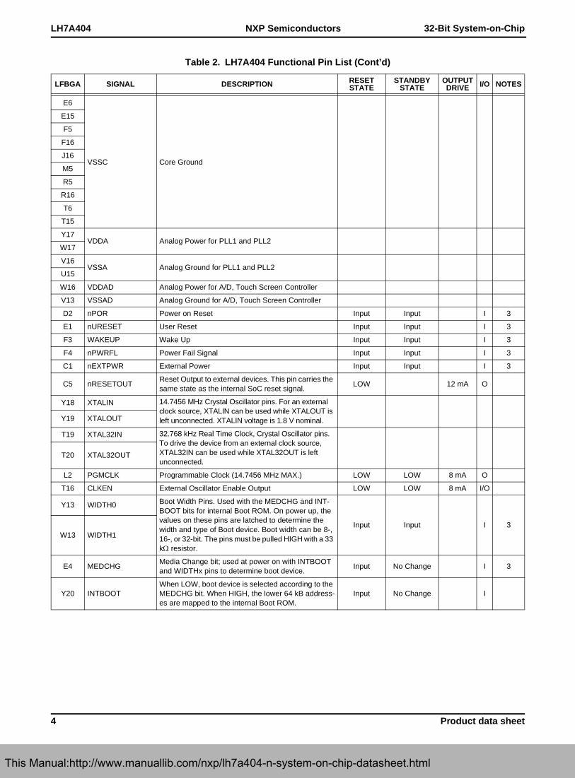
Table 2. LH7A404 Functional Pin List (Cont’d)
LFBGA SIGNAL DESCRIPTION RESETSTATE
STANDBY STATE
OUTPUTDRIVE I/O NOTES
This Manual:http://www.manuallib.com/nxp/lh7a404-n-system-on-chip-datasheet.html
32-Bit System-on-Chip LH7A404
Product data sheet 5
NXP Semiconductors
N19 D0
Data Bus LOW LOW 12 mA I/O
P20 D1
N18 D2
N20 D3
M16 D4
M18 D5
L18 D6
L17 D7
L19 D8
J19 D9
K17 D10
J18 D11
H19 D12
G20 D13
G19 D14
H17 D15
F19 D16
E20 D17
E19 D18
D20 D19
E18 D20
C20 D21
D18 D22
B20 D23
C18 D24
A20 D25
B18 D26
C16 D27
B17 D28
A18 D29
A17 D30
B15 D31
P17 A0Asynchronous Address Bus HIGH LOW 12 mA O
N16 A1
Table 2. LH7A404 Functional Pin List (Cont’d)
LFBGA SIGNAL DESCRIPTION RESETSTATE
STANDBY STATE
OUTPUTDRIVE I/O NOTES
This Manual:http://www.manuallib.com/nxp/lh7a404-n-system-on-chip-datasheet.html

LH7A404 32-Bit System-on-Chip
6 Product data sheet
NXP Semiconductors
N17 A2/SA0
Asynchronous Address Bus and Synchronous Address Bus
LOW LOW 12 mA O
M19 A3/SA1
M20 A4/SA2
L20 A5/SA3
M17 A6/SA4
K18 A7/SA5
K20 A8/SA6
K19 A9/SA7
J20 A10/SA8
H20 A11/SA9
J17 A12/SA10
H18 A13/SA11
F20 A14/SA12
G18 A15/SA13
H16 A16/SB0• Asynchronous Address Bus• Synchronous Device Bank Address 0
LOW LOW 12 mA O
F18 A17/SB1• Asynchronous Address Bus• Synchronous Device Bank Address 1
LOW LOW 12 mA O
G17 A18Asynchronous Address Bus LOW LOW 12 mA O
F17 A19
D19 A20 Asynchronous Address BusLOW LOW 12 mA O 4
E17 A21
C19 A22
Asynchronous Address BusLOW LOW 12 mA O
D17 A23
B19 A24
A16 A25
D15 A26
B14 A27
V18 nCS0 Asynchronous Memory Chip Select 0 HIGH HIGH 12 mA O
R19 nCS1 Asynchronous Memory Chip Select 1 HIGH HIGH 12 mA O
R18 nCS2 Asynchronous Memory Chip Select 2 HIGH HIGH 12 mA O
P19 nCS3 Asynchronous Memory Chip Select 3 HIGH HIGH 12 mA O
R20 nCS6 Asynchronous Memory Chip Select 6 HIGH No Change 12 mA O
R17 nCS7 Asynchronous Memory Chip Select 7 HIGH No Change 12 mA O
C12 nOE Asynchronous Memory Output Enable HIGH HIGH 12 mA O 4
D12 nWE Asynchronous Memory Write Enable HIGH HIGH 12 mA O 4
P18 nWAIT Asynchronous Memory Wait; pull HIGH if unused Input No Change I 5
C17 nSCS0 Synchronous Memory Chip Select 0 HIGH HIGH 12 mA I/O
A19 nSCS1 Synchronous Memory Chip Select 1 HIGH HIGH 12 mA I/O
D16 nSCS2 Synchronous Memory Chip Select 2 HIGH HIGH 12 mA I/O
E16 nSCS3 Synchronous Memory Chip Select 3 HIGH HIGH 12 mA I/O
B16 nSWE Synchronous Memory Write Enable HIGH HIGH 12 mA O
A14 SCKE0 Clock Enable 0 for Synchronous Memory HIGH No Change 12 mA O
B13 SCKE1_2 Clock Enable 1 OR 2 for Synchronous Memory HIGH No Change 12 mA O
Table 2. LH7A404 Functional Pin List (Cont’d)
LFBGA SIGNAL DESCRIPTION RESETSTATE
STANDBY STATE
OUTPUTDRIVE I/O NOTES
This Manual:http://www.manuallib.com/nxp/lh7a404-n-system-on-chip-datasheet.html

32-Bit System-on-Chip LH7A404
Product data sheet 7
NXP Semiconductors
C14 SCKE3 Clock Enable 3 for Synchronous MemoryDepends onMEDCHG
LOW 12 mA I/O
D14 SCLK Synchronous Memory Clock LOW No Change 20 mA I/O 2
A13 nBLE0 Byte Lane Enable 0 HIGH HIGH 12 mA I/O
U9 nBLE1 Byte Lane Enable 1 HIGH HIGH 12 mA O
Y7 nBLE2 Byte Lane Enable 2 HIGH HIGH 12 mA O
C13 nBLE3 Byte Lane Enable 3 HIGH HIGH 8 mA O
C15 nCAS Synchronous Memory Column Address Strobe HIGH HIGH 12 mA I/O
A15 nRAS Synchronous Memory Row Address Strobe HIGH HIGH 12 mA I/O
D13 DQM0
Data Mask for Synchronous Memories HIGH No Change 12 mA OE13 DQM1
B12 DQM2
A12 DQM3
M2PA0/LCDVD16
• GPIO Port A0• LCD Data pin 16
PA0: Input No Change 8 mA I/O
L4PA1/LCDVD17
• GPIO Port A1 • LCD Data pin 17
PA1: Input No Change 8 mA I/O
M3 PA2
GPIO Port A[6:2] PAx: Input No Change 8 mA I/O
M4 PA3
M1 PA4
N3 PA5
N2 PA6
N1 PA7• GPIO Port A7• Boot Width Selection (See Table 6)
PA7: Input No Change 8 mA I/O 4
N4 PB0/UARTRX1• GPIO Port B0• UART1 Receive Data Input
PB0: Input No Change 8 mA I/O
P3 PB1/UARTTX3• GPIO Port B1• UART3 Transmit Data Out
PB1: Input No Change 8 mA I/O
P2 PB2/UARTRX3• GPIO Port B2• UART3 Receive Data In
PB2: Input No Change 8 mA I/O
P1 PB3/UARTCTS3• GPIO Port B3• UART3 Clear to Send
PB3: Input No Change 8 mA I/O
R3 PB4/UARTDCD3• GPIO Port B4• UART3 Data Carrier Detect
PB4: Input No Change 8 mA I/O
N5 PB5/UARTDSR3• GPIO Port B5• UART3 Data Set Ready
PB5: Input No Change 8 mA I/O
R2 PB6/SWID/SMBD• GPIO Port B6• Single Wire Data• Smart Battery Data
PB6: Input No Change 8 mA I/O
R1 PB7/SMBCLK• GPIO Port B7• Smart Battery Clock
PB7: Input No Change 8 mA I/O
P4 PC0/UARTTX1• GPIO Port C0• UART1 Transmit Data Output
PC0: LOW No Change 12 mA I/O
T1 PC1
GPIO Port C[5:1] PCx: LOW No Change 12 mA I/O
T2 PC2
T3 PC3
R4 PC4
U1 PC5
U2 PC6 GPIO Port C6 PC6: LOW No Change 12 mA I/O 4
Table 2. LH7A404 Functional Pin List (Cont’d)
LFBGA SIGNAL DESCRIPTION RESETSTATE
STANDBY STATE
OUTPUTDRIVE I/O NOTES
This Manual:http://www.manuallib.com/nxp/lh7a404-n-system-on-chip-datasheet.html

LH7A404 32-Bit System-on-Chip
8 Product data sheet
NXP Semiconductors
V1 PC7 GPIO Port C7 PC7: LOW No Change 12 mA I/O
Y11 PD0/LCDVD8
• GPIO Port D[7:0]• LCD Video Data Interface
PDx: LOW
LOW if 8-bit LCD
enabled; else No Change
12 mA I/O
U10 PD1/LCDVD9
W12 PD2/LCDVD10
V11 PD3/LCDVD11
W11 PD4/LCDVD12
U11 PD5/LCDVD13
V12 PD6/LCDVD14
Y12 PD7/LCDVD15
Y9 PE0/LCDVD4
• GPIO Port E[3:0]• LCD Video Data Interface
PEx: Output
LOW if 8-bit LCD
enabled; else No Change
12 mA I/OW10 PE1/LCDVD5
V10 PE2/LCDVD6
T9 PE3/LCDVD7
D4 PE4/SCCLKIN• GPIO Port E4• Smart Card Push-Pull Mode Clock Input
PE4: Output No Change 12 mA I/O
C3 PE5/SCCLKEN• GPIO Port E5• Smart Card Push-Pull Mode External Clock
Buffer EnablePE5: Output No Change 12 mA I/O
B2 PE6/SCIN• GPIO Port E6• Smart Card Push-Pull Mode Data Input
PE6: Output No Change 12 mA I/O
A1 PE7/SCDATEN• GPIO Port E7• Smart Card Push-Pull Mode Data Out External
Buffer EnablePE7: Output No Change 12 mA I/O
A9 PF0/INT0• GPIO Port F0• Interrupt 0
PF0: Input No Change 8 mA I/O 3
D9 PF1/INT1• GPIO Port F1• Interrupt 1
PF1: Input No Change 8 mA I/O 3
A8 PF2/INT2• GPIO Port F2• Interrupt 2
PF2: Input No Change 8 mA I/O 3
C8 PF3/INT3• GPIO Port F3• Interrupt 3
PF3: Input No Change 8 mA I/O 3
B8 PF4/INT4• GPIO Port F4• Interrupt 4
PF4: Input No Change 8 mA I/O 3
D8PF5/INT5/SCDETECT
• GPIO Port F5• Interrupt 5• Smart Card Interface Card Detect Signal
PF5: Input No Change 8 mA I/O 3
A7PF6/INT6/PCRDY1
• GPIO Port F6• Interrupt 6• Ready for Card 1 for PC Card (PCMCIA or
CompactFlash) in Single or Dual Card mode
PF6: Input No Change 8 mA I/O 3
E8 PF7/INT7/PCRDY2
• GPIO Port F7• Interrupt 7• Ready for Card 2 for PC Card (PCMCIA or
CompactFlash) in Single or Dual Card mode
PF7: Input No Change 8 mA I/O 3
Y2 PG0/nPCOE• GPIO Port G0• Output Enable for PC Card (PCMCIA or
CompactFlash) in Single or Dual Card modeLOW No Change 8 mA I/O
W4 PG1/nPCWE• GPIO Port G1• Write Enable for PC Card (PCMCIA or
CompactFlash) in Single or Dual Card modeLOW No Change 8 mA I/O
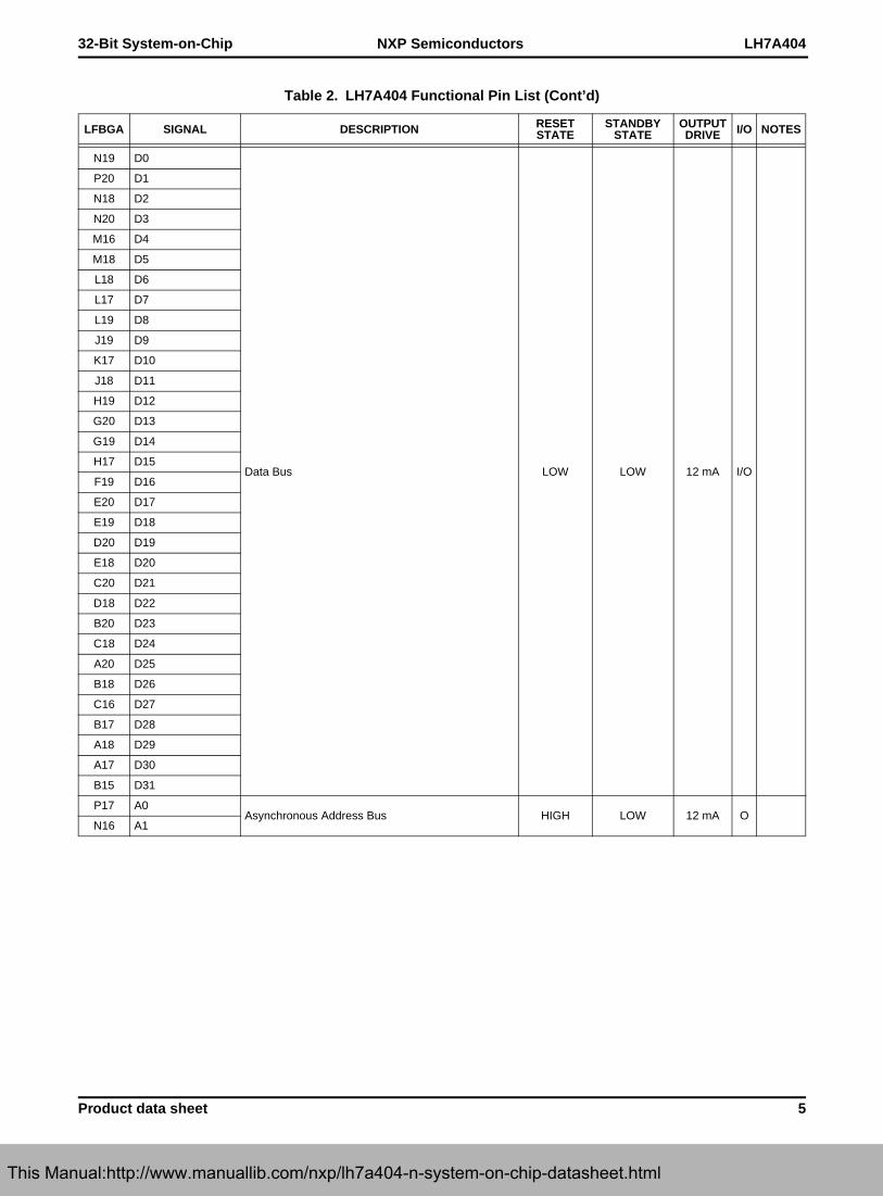
Table 2. LH7A404 Functional Pin List (Cont’d)
LFBGA SIGNAL DESCRIPTION RESETSTATE
STANDBY STATE
OUTPUTDRIVE I/O NOTES
This Manual:http://www.manuallib.com/nxp/lh7a404-n-system-on-chip-datasheet.html

32-Bit System-on-Chip LH7A404
Product data sheet 9
NXP Semiconductors
Y3 PG2/nPCIOR• GPIO Port G2• I/O Read Strobe for PC Card (PCMCIA or
CompactFlash) in Single or Dual Card modeLOW No Change 8 mA I/O
U5 PG3/nPCIOW• GPIO Port G3• I/O Write Strobe for PC Card (PCMCIA or
CompactFlash) in Single or Dual Card modeLOW No Change 8 mA I/O
T5 PG4/nPCREG• GPIO Port G4• Register Memory Access for PC Card (PCMCIA or
CompactFlash) in Single or Dual Card modeLOW No Change 8 mA I/O
W5 PG5/nPCCE1
• GPIO Port G5• Card Enable 1 for PC Card (PCMCIA or
CompactFlash) in Single or Dual Card mode. This signal and nPCCE2 are used by the PC Card for decoding low and high byte accesses.
LOW No Change 8 mA I/O
Y4 PG6/nPCCE2
• GPIO Port G6• Card Enable 2 for PC Card (PCMCIA or
CompactFlash) in Single or Dual Card mode. This signal and nPCCE1 are used by the PC Card for decoding low and high byte accesses.
LOW No Change 8 mA I/O
W6 PG7/PCDIR• GPIO Port G7• Direction for PC Card (PCMCIA or CompactFlash)
in Single or Dual Card modeLOW No Change 8 mA I/O
V6 PH0/PCRESET1• GPIO Port H0• Reset Card 1 for PC Card (PCMCIA or
CompactFlash) in Single or Dual Card modePHx: Input No Change 8 mA I/O
Y5PH1/CFA8/PCRESET2
• GPIO Port H1• Address Bit 8 for PC Card (CompactFlash) in
Single Card mode• Reset Card 2 for PC Card (PCMCIA or
CompactFlash) in Dual Card mode
PHx: Input No Change 8 mA I/O
W7 PH2/nPCSLOTE1
• GPIO Port H2• Enable Card 1 for PC Card (PCMCIA or
CompactFlash) in Single or Dual Card mode. This signal is used for gating other control signals to the appropriate PC Card.
PHx: Input No Change 8 mA I/O
U6PH3/CFA9/PCMCIAA25/nPCSLOTE2
• GPIO Port H3• Address Bit 9 for PC Card (CompactFlash) in Single
Card mode • Address Bit 25 for PC Card (PCMCIA) in
Single Card mode• Enable Card 2 for PC Card (PCMCIA or
CompactFlash) in Dual Card mode. Used for gating other control signals to the appropriate PC Card.
PHx: Input No Change 8 mA I/O
W8 PH4/nPCWAIT1• GPIO Port H4• WAIT Signal for Card 1 for PC Card (PCMCIA or
CompactFlash) in Single or Dual Card modePHx: Input No Change 8 mA I/O
Y6PH5/CFA10/PCMCIAA24/nPCWAIT2
• GPIO Port H5• Address Bit 10 for PC Card (CompactFlash) in Sin-
gle Card mode• Address Bit 24 for PC Card (PCMCIA) in Single
Card mode• WAIT Signal for Card 2 for PC Card (PCMCIA or
CompactFlash) in Dual Card mode
PHx: Input No Change 8 mA I/O
V7 PH6/nAC97RESET• GPIO Port H6• AC97 Reset
PHx: Input No Change 8 mA I/O
Table 2. LH7A404 Functional Pin List (Cont’d)
LFBGA SIGNAL DESCRIPTION RESETSTATE
STANDBY STATE
OUTPUTDRIVE I/O NOTES
This Manual:http://www.manuallib.com/nxp/lh7a404-n-system-on-chip-datasheet.html
LH7A404 32-Bit System-on-Chip
10 Product data sheet
NXP Semiconductors
U7PH7/nPCSTATRE
• GPIO Port H7• Status Read Enable for PC Card (PCMCIA or
CompactFlash) in Single or Dual Card modePHx: Input No Change 8 mA I/O
T4 LCDFP/LCDSPS• LCD Frame Pulse• ALI Reset Row Driver Counter
LOWLOW if not in
ALI mode12 mA O
V2LCDLP/LCDHRLP
• LCD Linepulse• ALI Latch Pulse
LOWLOW if not in
ALI mode12 mA O
U3 LCDCLS ALI Clock for Row Drivers LOW No Change 12 mA O
V3 LCDSPL ALI Start Pulse Left for reverse scanning LOW No Change 12 mA O
U4 LCDUBL ALI Up, Down signal for reverse scanning LOW No Change 12 mA O
W1 LCDSPR ALI Start Pulse Right for normal scanning LOW No Change 12 mA O
V4 LCDLBR ALI Output for reverse scanning HIGH No Change 12 mA O
W2 LCDMOD ALI MOD Signal used by the row driver LOW No Change 12 mA O
V5 LCDPS ALI Power Save HIGH No Change 12 mA O
Y1 LCDVDDEN ALI Power Sequence Control LOW No Change 12 mA O
W3 LCDREV ALI Reverse HIGH No Change 12 mA O
U8 LCDCLKIN External Clock Input for LCD controller Input No Change I
V8 LCDVD0
LCD Video Data Interface LOW LOW 12 mA OT8 LCDVD1
W9 LCDVD2
Y8 LCDVD3
V9LCDENAB/LCDM
• LCD TFT Data Enable• LCD STN AC Bias
LOW LOW 12 mA O
Y10 LCDDCLK LCD Pixel Clock LOW LOW 12 mA O
U17 USBDCP USB Device Full Speed Pull-up Resistor Control Input Input 12 mA I
U20 USBDP USB Device Data Positive (Differential Pair) Input Input 12 mA I/O
U19 USBDN USB Device Data Negative (Differential Pair) Input Input 12 mA I/O
W19 USBHDP0 USB Data Host Positive 0 (Differential Pair) Input HIGH 12 mA I/O
W20 USBHDN0 USB Data Host Negative 0 (Differential Pair) Input LOW 12 mA I/O
V19 USBHDP1 USB Data Host Positive 1 (Differential Pair) Input Input 12 mA I/O
V20 USBHDN1 USB Data Host Negative 1 (Differential Pair) Input Input 12 mA I/O
T17 USBHPWR
USB Host Power; This pin is connected to the remote USB Host Power Switch’s Enable pin. In response to a fault condition, signalled on the nUSBHOVRCURR pin, the LH7A404 can assert this pin, which causes the power switch shut down.
LOW No Change 12 mA O
V17 nUSBHOVRCURR
USB Host Overcurrent; The overcurrent input is used to indicate to the host a fault has occurred, resulting in current limiting. The LH7A404 can be programmed to cause the remote power switch to shut off by assert-ing USBHPWR in response to an nUSBHOVRCURR assertion.
Input Input 12 mA I
D11 nPWME0 DC-DC Converter 0 PWM 0 Enable Input Input 8 mA I/O
A10 nPWME1 DC-DC Converter 1 PWM 1 Enable Input Input 8 mA I/O
C11 PWM0 DC-DC Converter 0 Output (Pulse Width Modulated) LOW Input 8 mA I/O
C10 PWM1 DC-DC Converter 1 Output (Pulse Width Modulated) LOW Input 8 mA I/O
B9 PWM2 PWM Output 2 LOW No Change 8 mA O
D10 PWM3 PWM Output 3 LOW No Change O
C9 PWMSYNC PWM Synchronizing Input for PWM2 Input No Change 8 mA I
Table 2. LH7A404 Functional Pin List (Cont’d)
LFBGA SIGNAL DESCRIPTION RESETSTATE
STANDBY STATE
OUTPUTDRIVE I/O NOTES
This Manual:http://www.manuallib.com/nxp/lh7a404-n-system-on-chip-datasheet.html

32-Bit System-on-Chip LH7A404
Product data sheet 11
NXP Semiconductors
C7 ACBITCLK• Audio Codec (AC97) Clock• Audio Codec (ACI) Clock
Input No Change 8 mA I/O
B7 ACOUT• Audio Codec (AC97) Output• Audio Codec (ACI) Output
LOW LOW 8 mA O
A6 ACSYNC• Audio Codec (AC97) Synchronization• Audio Codec (ACI) Synchronization
LOW LOW 8 mA O
B6 ACIN• Audio Codec (AC97) Input• Audio Codec (ACI) Input
Input No Change 8 mA I/O
A5 MMCCLK MultiMediaCard Clock (20 MHz MAX.) LOW LOW 8 mA I/O
D7 MMCCMD MultiMediaCard Command Input Input 8 mA I/O
C6 MMCDATA0 MultiMediaCard Data 0 Input Input 8 mA I/O
B5 MMCDATA1 MultiMediaCard Data 1 Input Input 8 mA I/O
A4 MMCDATA2 MultiMediaCard Data 2 Input Input 8 mA I/O
B4 MMCDATA3 MultiMediaCard Data 3 Input Input 8 mA I/O
F2 UARTCTS2 UART2 Clear to Send Signal Input Input 8 mA I/O
F1 UARTDCD2 UART2 Data Carrier Detect Signal Input Input 8 mA I/O
G2 UARTDSR2 UART2 Data Set Ready Signal Input Input 8 mA I/O
G3 UARTIRTX1 IrDA Transmit LOW No Change 8 mA I/O
G1 UARTIRRX1 IrDA Receive Input Input 8 mA I/O
H2 UARTTX2 UART2 Transmit Data Output HIGH No Change 8 mA I/O
G4 UARTRX2 UART2 Receive Data Input Input Input 8 mA I/O
K3 SSPCLK Synchronous Serial Port Clock LOW LOW 8 mA O
L1 SSPRX Synchronous Serial Port Receive Input Input 8 mA I/O
L3 SSPTX Synchronous Serial Port Transmit Input Input 8 mA I/O
K4 SSPFRM Synchronous Serial Port Frame Sync HIGH HIGH 8 mA O
J2 COL0
Keyboard Interface HIGH HIGH 8 mA I/O
H4 COL1
H5 COL2
J1 COL3
J3 COL4
J4 COL5
J5 COL6
K2 COL7
E2 BATOK Battery OK Input Input I 3
D1 nBATCHG Battery Change Input Input I 3
U12 BATCNTL Battery Control for A/D controller battery monitor LOW No Change 12 mA O
H1 KMIDAT Keyboard/Mouse Data Input No Change 12 mA I/O
H3 KMICLK Keyboard/Mouse Clock Input No Change 12 mA I/O
K1 TBUZ Timer Buzzer Output (254 kHz MAX.) LOW LOW 8 mA I/O
Y16 AN0/UL/X+• ADC channel 0• Touch Screen Controller Upper Left• Touch Screen Controller X-plus
Input Input I
Y15 AN1/UR/X-• ADC channel 1• Touch Screen Controller Upper Right• Touch Screen Controller X-minus
Input Input I
W14 AN2/LL/Y+• ADC channel 2• Touch Screen Controller Lower Left• Touch Screen Controller Y-plus
Input Input I
Table 2. LH7A404 Functional Pin List (Cont’d)
LFBGA SIGNAL DESCRIPTION RESETSTATE
STANDBY STATE
OUTPUTDRIVE I/O NOTES
This Manual:http://www.manuallib.com/nxp/lh7a404-n-system-on-chip-datasheet.html

LH7A404 32-Bit System-on-Chip
12 Product data sheet
NXP Semiconductors
NOTES:1. Signals beginning with ‘n’ are Active LOW.2. The SCLK pin can source up to 12 mA and sink up to 20 mA.
See ‘DC Characteristics’.3. Schmitt trigger input; see ’DC Specifications’, page 31 for triggers
points and hysteresis.4. These pins have alternate NAND Flash functions during boot-up
when using the internal Boot ROM. Consult the Boot ROMChapter of the User’s Guide for more information.
5. The nWAIT pin must be pulled HIGH with a 33 k resistor to avoidthe possibility of the SMC inadvertently going into WAIT.
6. The internal pullup and pulldown resistance on all digital I/O pinsis 50K.
U13 AN3/LR/Y-• ADC channel 3• Touch Screen Controller Lower Right• Touch Screen Controller Y-minus
Input Input I
V14 AN4/WIPER• ADC channel 4• Wiper input from 5-wire Touch Screen
Input Input I
U14 VSS or VSSA Connect pin to either VSS or VSSA Input Input I
V15 AN6 ADC channel 6 Input Input I
W15 AN7 ADC channel 7 Input Input I
T13 AN8 ADC channel 8 Input Input I
Y14 AN9 ADC channel 9 Input Input I
E12 SCIO Smart Card Interface I/O LOW LOW 12 mA I/O
A11 SCCLK Smart Card Interface Clock LOW LOW 12 mA I/O
B11 nSCRESET Smart Card Interface Reset LOW LOW 12 mA O
B10 SCVCCEN Smart Card Interface VCC Enable LOW No Change 12 mA O
D6 CTCLKIN Counter Timer Clock Input Input No Change I
A3 DREQ0 DMA Request 0 Input No Change I
D5 DACK0 DMA Acknowledge 0 Input No Change 12 mA I/O
C4 DEOT0 DMA End of Transfer 0 Input No Change 12 mA I/O
B3 DREQ1 DMA Request 1 Input No Change I
A2 DACK1 DMA Acknowledge 1 Input No Change 12 mA I/O
E5 DEOT1 DMA End of Transfer 1 Input No Change 12 mA I/O
U16 nTEST0
Test Pin 0. Internal weak pull up to VDD. Status latched at nPOR going HIGH. Pull LOW for JTAG mode. Pull HIGH (or leave open) for Normal mode. See Table 3.
Input with pull-up
Input with pull-up
I
W18 nTEST1Test Pin 1. Internal weak pull up to VDD. Status latched at nPOR going HIGH. Pull HIGH (or leave open) for both JTAG and Normal mode. See Table 3.
Input with pull-up
Input with pull-up
I
D3 TDI JTAG Data In. Internal weak pull up to VDD. Input No Change I
C2 TCK JTAG Clock. Internal weak pull up to VDD. Input No Change I 3
B1 TDO JTAG Data Out High Z No Change 4 mA O
E3 TMSJTAG Test Mode Select. Internal weak pull up to VDD.
Input No Change I
Table 2. LH7A404 Functional Pin List (Cont’d)
LFBGA SIGNAL DESCRIPTION RESETSTATE
STANDBY STATE
OUTPUTDRIVE I/O NOTES
Table 3. nTEST Pin Function
MODE nTEST0 nTEST1 nURESET
JTAG 0 1 1
Normal 1 1 x
This Manual:http://www.manuallib.com/nxp/lh7a404-n-system-on-chip-datasheet.html

32-Bit System-on-Chip LH7A404
Product data sheet 13
NXP Semiconductors
NOTES:1. The Intensity bit is identically generated for all three colors.2. MUSTN = Monochrome Upper Panel
MLSTN = Monochrome Lower PanelCUSTN = Color Upper PanelCLSTN = Color Lower Panel
Table 4. LCD Controller Pins
LFBGAPIN
RESETSTATE
LCD SIGNAL
STN
TFT AD-TFT/HR-TFT
MONO 4-BIT MONO 8-BIT COLOR
SINGLEPANEL
DUALPANEL
SINGLEPANEL
DUALPANEL
SINGLEPANEL
DUALPANEL
L4 PA1 LCDVD17 LOW
M2 PA0 LCDVD16 LOW
Y12 PD7 LCDVD15 MLSTN7 CLSTN7 Intensity Intensity
V12 PD6 LCDVD14 MLSTN6 CLSTN6 BLUE4 BLUE4
U11 PD5 LCDVD13 MLSTN5 CLSTN5 BLUE3 BLUE3
W11 PD4 LCDVD12 MLSTN4 CLSTN4 BLUE2 BLUE2
V11 PD3 LCDVD11 MLSTN3 CLSTN3 BLUE1 BLUE1
W12 PD2 LCDVD10 MLSTN2 CLSTN2 BLUE0 BLUE0
U10 PD1 LCDVD9 MLSTN1 CLSTN1 GREEN4 GREEN4
Y11 PD0 LCDVD8 MLSTN0 CLSTN0 GREEN3 GREEN3
T9 PE3 LCDVD7 MLSTN3 MUSTN7 MUSTN7 CUSTN7 CUSTN7 GREEN2 GREEN2
V10 PE2 LCDVD6 MLSTN2 MUSTN6 MUSTN6 CUSTN6 CUSTN6 GREEN1 GREEN1
W10 PE1 LCDVD5 MLSTN1 MUSTN5 MUSTN5 CUSTN5 CUSTN5 GREEN0 GREEN0
Y9 PE0 LCDVD4 MLSTN0 MUSTN4 MUSTN4 CUSTN4 CUSTN4 RED4 RED4
Y8 LCDVD3 LCDVD3 MUSTN3 MUSTN3 MUSTN3 MUSTN3 CUSTN3 CUSTN3 RED3 RED3
W9 LCDVD2 LCDVD2 MUSTN2 MUSTN2 MUSTN2 MUSTN2 CUSTN2 CUSTN2 RED2 RED2
T8 LCDVD1 LCDVD1 MUSTN1 MUSTN1 MUSTN1 MUSTN1 CUSTN1 CUSTN1 RED1 RED1
V8 LCDVD0 LCDVD0 MUSTN0 MUSTN0 MUSTN0 MUSTN0 CUSTN0 CUSTN0 RED0 RED0
U3 LCDCLS LCDCLS LCDCLS
Y10 LCDDCLK LCDDCLK LCDDCLK LCDDCLK LCDDCLK LCDDCLK LCDDCLK LCDDCLK LCDDCLK LCDDCLK
T4 LCDFPLCDFP/LCDSPS
LCDFP LCDFP LCDFP LCDFP LCDFP LCDFP LCDFP LCDSPS
V2 LCDLPLCDLP/
LCDHRLPLCDLP LCDLP LCDLP LCDLP LCDLP LCDLP LCDLP LCDHRLP
W2 LCDMOD LCDMOD LCDMOD
V5 LCDPS LCDPS LCDPS
W3 LCDREV LCDREV LCDREV
V3 LCDSPL LCDSPL LCDSPL
V4 LCDLBR LCDLBR LCDLBR
W1 LCDSPR LCDSPR LCDSPR
U4 LCDUBL LCDUBL LCDUBL
Y1 LCDVDDEN LCDVDDEN LCDVDDEN
U8 LCDCLKIN LCDCLKIN LCDCLKIN LCDCLKIN LCDCLKIN LCDCLKIN LCDCLKIN LCDCLKIN LCDCLKIN LCDCLKIN
V9 LCDENABLCDENAB/
LCDMLCDM LCDM LCDM LCDM LCDM LCDM LCDENAB
This Manual:http://www.manuallib.com/nxp/lh7a404-n-system-on-chip-datasheet.html

LH7A404 32-Bit System-on-Chip
14 Product data sheet
NXP Semiconductors
Table 5. LFBGA Numerical Pin List
LFBGA SIGNAL SLEWRATE
OUTPUTDRIVE
A1 PE7/SCDATEN 95 mV/ns 12 mA
A2 DACK1 95 mV/ns 12 mA
A3 DREQ0
A4 MMCDATA2 110 mV/ns 8 mA
A5 MMCCLK 110 mV/ns 8 mA
A6 ACSYNC 110 mV/ns 8 mA
A7 PF6/INT6/PCRDY1 110 mV/ns 8 mA
A8 PF2/INT2 110 mV/ns 8 mA
A9 PF0/INT0 110 mV/ns 8 mA
A10 nPWME1 95 mV/ns 12 mA
A11 SCCLK 95 mV/ns 12 mA
A12 DQM3 110 mV/ns 8 mA
A13 nBLE0 95 mV/ns 12 mA
A14 SCKE0 95 mV/ns 12 mA
A15 nRAS 95 mV/ns 12 mA
A16 A25 95 mV/ns 12 mA
A17 D30 95 mV/ns 12 mA
A18 D29 95 mV/ns 12 mA
A19 nSCS1 95 mV/ns 12 mA
A20 D25 95 mV/ns 12 mA
B1 TDO 100 mV/ns 4 mA
B2 PE6/SCIN 95 mV/ns 12 mA
B3 DREQ1
B4 MMCDATA3 110 mV/ns 8 mA
B5 MMCDATA1 110 mV/ns 8 mA
B6 ACIN 110 mV/ns 8 mA
B7 ACOUT 110 mV/ns 8 mA
B8 PF4/INT4 110 mV/ns 8 mA
B9 PWM2 110 mV/ns 8 mA
B10 SCVCCEN 95 mV/ns 12 mA
B11 nSCRESET 95 mV/ns 12 mA
B12 DQM2 95 mV/ns 12 mA
B13 SCKE1_2 95 mV/ns 12 mA
B14 A27 95 mV/ns 12 mA
B15 D31 95 mV/ns 12 mA
B16 nSWE 95 mV/ns 12 mA
B17 D28 95 mV/ns 12 mA
B18 D26 95 mV/ns 12 mA
B19 A24 95 mV/ns 12 mA
B20 D23 95 mV/ns 12 mA
C1 nEXTPWR
C2 TCK
C3 PE5/SCCLKEN 95 mV/ns 12 mA
C4 DEOT0 95 mV/ns 12 mA
C5 nRESETOUT
C6 MMCDATA 110 mV/ns 8 mA
C7 ACBITCLK 110 mV/ns 8 mA
C8 PF3/INT3 110 mV/ns 8 mA
C9 PWMSYNC
C10 PWM1 110 mV/ns 8 mA
C11 PWM0 110 mV/ns 8 mA
C12 nOE 95 mV/ns 12 mA
C13 nBLE3 110 mV/ns 8 mA
C14 SCKE3 95 mV/ns 12 mA
C15 nCAS 95 mV/ns 12 mA
C16 D27 95 mV/ns 12 mA
C17 nSCS0 95 mV/ns 12 mA
C18 D24 95 mV/ns 12 mA
C19 A22 95 mV/ns 12 mA
C20 D21 95 mV/ns 12 mA
D1 nBATCHG
D2 nPOR
D3 TDI
D4 PE4/SCCLKIN 95 mV/ns 12 mA
D5 DACK0 95 mV/ns 12 mA
D6 CTCLKIN
D7 MMCCMD 110 mV/ns 8 mA
D8 PF5/INT5/SCDETECT 110 mV/ns 8 mA
D9 PF1/INT1 110 mV/ns 8 mA
D10 PWM3 110 mV/ns 8 mA
D11 nPWME0 110 mV/ns 8 mA
D12 nWE 95 mV/ns 12 mA
D13 DQM0 95 mV/ns 12 mA
D14 SCLK 190 mV/ns 20 mA
D15 A26 95 mV/ns 12 mA
D16 nSCS2 95 mV/ns 12 mA
D17 A23 95 mV/ns 12 mA
D18 D22 95 mV/ns 12 mA
D19 A20 95 mV/ns 12 mA
D20 D19 95 mV/ns 12 mA
E1 nURESET
E2 BATOK
E3 TMS
E4 MEDCHG
E5 DEOT1 95 mV/ns 12 mA
E6 VSSC
E7 VDDC
E8 PF7/INT7/PCRDY2 110 mV/ns 8 mA
E9 VDDC
E10 VDD
Table 5. LFBGA Numerical Pin List (Cont’d)
LFBGA SIGNAL SLEWRATE
OUTPUTDRIVE
This Manual:http://www.manuallib.com/nxp/lh7a404-n-system-on-chip-datasheet.html

32-Bit System-on-Chip LH7A404
Product data sheet 15
NXP Semiconductors
E11 VDD
E12 SCIO 95 mV/ns 12 mA
E13 DQM1 95 mV/ns 12 mA
E14 VDDC
E15 VSSC
E16 nSCS3 95 mV/ns 12 mA
E17 A21 95 mV/ns 12 mA
E18 D20 95 mV/ns 12 mA
E19 D18 95 mV/ns 12 mA
E20 D17 95 mV/ns 12 mA
F1 UARTDCD2 110 mV/ns 8 mA
F2 UARTCTS2 110 mV/ns 8 mA
F3 WAKEUP
F4 nPWRFL
F5 VSSC
F16 VSSC
F17 A19 95 mV/ns 12 mA
F18 A17/SBANK1 95 mV/ns 12 mA
F19 D16 95 mV/ns 12 mA
F20 A14/SA12 95 mV/ns 12 mA
G1 UARTIRRX1 110 mV/ns 8 mA
G2 UARTDSR2 110 mV/ns 8 mA
G3 UARTIRTX1 110 mV/ns 8 mA
G4 UARTRX2 110 mV/ns 8 mA
G5 VDDC
G16 VDDC
G17 A18 95 mV/ns 12 mA
G18 A15/SA13 95 mV/ns 12 mA
G19 D14 95 mV/ns 12 mA
G20 D13 95 mV/ns 12 mA
H1 KMIDAT 95 mV/ns 12 mA
H2 UARTTX2 110 mV/ns 8 mA
H3 KMICLK 95 mV/ns 12 mA
H4 COL1 100 mV/ns 8 mA
H5 COL2 100 mV/ns 8 mA
H10 VDD
H11 VDD
H16 A16/SBANK0 95 mV/ns 12 mA
H17 D15 95 mV/ns 12 mA
H18 A13/SA11 95 mV/ns 12 mA
H19 D12 95 mV/ns 12 mA
H20 A11/SA9 95 mV/ns 12 mA
J1 COL3 100 mV/ns 8 mA
J2 COL0 100 mV/ns 8 mA
J3 COL4 100 mV/ns 8 mA
Table 5. LFBGA Numerical Pin List (Cont’d)
LFBGA SIGNAL SLEWRATE
OUTPUTDRIVE
J4 COL5 100 mV/ns 8 mA
J5 COL6 100 mV/ns 8 mA
J9 VSS
J10 VSS
J11 VSS
J12 VSS
J16 VSSC
J17 A12/SA10 95 mV/ns 12 mA
J18 D11 95 mV/ns 12 mA
J19 D9 95 mV/ns 12 mA
J20 A10/SA8 95 mV/ns 12 mA
K1 TBUZ 110 mV/ns 8 mA
K2 COL7 100 mV/ns 8 mA
K3 SSPCLK 110 mV/ns 8 mA
K4 SSPFRM 110 mV/ns 8 mA
K5 VDD
K8 VDD
K9 VSS
K10 VSS
K11 VSS
K12 VSS
K13 VDD
K16 VDD
K17 D10 95 mV/ns 12 mA
K18 A7/SA5 95 mV/ns 12 mA
K19 A9/SA7 95 mV/ns 12 mA
K20 A8/SA6 95 mV/ns 12 mA
L1 SSPRX 110 mV/ns 8 mA
L2 PGMCLK 110 mV/ns 8 mA
L3 SSPTX 110 mV/ns 8 mA
L4 PA1/LCDVD17 110 mV/ns 8 mA
L5 VDD
L8 VDD
L9 VSS
L10 VSS
L11 VSS
L12 VSS
L13 VDD
L16 VDD
L17 D7 95 mV/ns 12 mA
L18 D6 95 mV/ns 12 mA
L19 D8 95 mV/ns 12 mA
L20 A5/SA3 95 mV/ns 12 mA
M1 PA4 110 mV/ns 8 mA
M2 PA0/LCDVD16 110 mV/ns 8 mA
Table 5. LFBGA Numerical Pin List (Cont’d)
LFBGA SIGNAL SLEWRATE
OUTPUTDRIVE
This Manual:http://www.manuallib.com/nxp/lh7a404-n-system-on-chip-datasheet.html

LH7A404 32-Bit System-on-Chip
16 Product data sheet
NXP Semiconductors
M3 PA2 110 mV/ns 8 mA
M4 PA3 110 mV/ns 8 mA
M5 VSSC
M9 VSS
M10 VSS
M11 VSS
M12 VSS
M16 D4 95 mV/ns 12 mA
M17 A6/SA4 95 mV/ns 12 mA
M18 D5 95 mV/ns 12 mA
M19 A3/SA1 95 mV/ns 12 mA
M20 A4/SA2 95 mV/ns 12 mA
N1 PA7 110 mV/ns 8 mA
N2 PA6 110 mV/ns 8 mA
N3 PA5 110 mV/ns 8 mA
N4 PB0/UARTRX1 110 mV/ns 8 mA
N5 PB5/UARTDSR3 110 mV/ns 8 mA
N10 VDD
N11 VDD
N16 A1 95 mV/ns 12 mA
N17 A2/SA0 95 mV/ns 12 mA
N18 D2 95 mV/ns 12 mA
N19 D0 95 mV/ns 12 mA
N20 D3 95 mV/ns 12 mA
P1 PB3/UARTCTS3 110 mV/ns 8 mA
P2 PB2/UARTRX3 110 mV/ns 8 mA
P3 PB1/UARTTX3 110 mV/ns 8 mA
P4 PC0/UARTTX1 95 mV/ns 12 mA
P5 VDDC
P16 VDDC
P17 A0 95 mV/ns 12 mA
P18 nWAIT
P19 nCS3 95 mV/ns 12 mA
P20 D1 95 mV/ns 12 mA
R1 PB7/SMBCLK 110 mV/ns 8 mA
R2 PB6/SWID/SMBD 110 mV/ns 8 mA
R3 PB4/UARTDCD3 110 mV/ns 8 mA
R4 PC4 95 mV/ns 12 mA
R5 VSSC
R16 VSSC
R17 nCS7 95 mV/ns 12 mA
R18 nCS2 95 mV/ns 12 mA
R19 nCS1 95 mV/ns 12 mA
R20 nCS6 95 mV/ns 12 mA
T1 PC1 95 mV/ns 12 mA
Table 5. LFBGA Numerical Pin List (Cont’d)
LFBGA SIGNAL SLEWRATE
OUTPUTDRIVE
T2 PC2 95 mV/ns 12 mA
T3 PC3 95 mV/ns 12 mA
T4 LCDFP/LCDSPS 95 mV/ns 12 mA
T5 PG4/nPCREG 110 mV/ns 8 mA
T6 VSSC
T7 VDDC
T8 LCDVD1 95 mV/ns 12 mA
T9 PE3/LCDVD7 95 mV/ns 12 mA
T10 VDD
T11 VDD
T12 VDDC
T13 AN8
T14 VDDC
T15 VSSC
T16 CLKEN 110 mV/ns 8 mA
T17 USBHPWR 95 mV/ns 12 mA
T18 VSS
T19 XTAL32IN
T20 XTAL32OUT
U1 PC5 95 mV/ns 12 mA
U2 PC6 95 mV/ns 12 mA
U3 LCDCLS 95 mV/ns 12 mA
U4 LCDUBL 95 mV/ns 12 mA
U5 PG3/nPCIOW 110 mV/ns 8 mA
U6PH3/CFA9/PCMCIAA25/nPCSLOTE2
110 mV/ns 8 mA
U7 PH7/nPCSTATRE 110 mV/ns 8 mA
U8 LCDCLKIN
U9 nBLE1 95 mV/ns 12 mA
U10 PD1/LCDVD9 95 mV/ns 12 mA
U11 PD5/LCDVD13 95 mV/ns 12 mA
U12 BATCTL 95 mV/ns 12 mA
U13 AN3/LR/Y-
U14 VSS or VSSA
U15 VSSA
U16 nTEST0
U17 USBDCP
U18 VDD
U19 USBDN
U20 USBDP
V1 PC7 95 mV/ns 12 mA
V2 LCDLP/LCDHRLP 95 mV/ns 12 mA
V3 LCDSPL 95 mV/ns 12 mA
V4 LCDLBR 95 mV/ns 12 mA
V5 LCDPS 95 mV/ns 12 mA
Table 5. LFBGA Numerical Pin List (Cont’d)
LFBGA SIGNAL SLEWRATE
OUTPUTDRIVE
This Manual:http://www.manuallib.com/nxp/lh7a404-n-system-on-chip-datasheet.html

32-Bit System-on-Chip LH7A404
Product data sheet 17
NXP Semiconductors
V6 PH0/PCRESET1 110 mV/ns 8 mA
V7 PH6/nAC97RESET 110 mV/ns 8 mA
V8 LCDVD0 95 mV/ns 12 mA
V9 LCDENAB/LCDM 95 mV/ns 12 mA
V10 PE2/LCDVD6 95 mV/ns 12 mA
V11 PD3/LCDVD11 95 mV/ns 12 mA
V12 PD6/LCDVD14 95 mV/ns 12 mA
V13 VSSAD
V14 AN4/WIPER
V15 AN6
V16 VSSA
V17 nUSBHOVRCURR
V18 nCS0 95 mV/ns 12 mA
V19 USBHDP1
V20 USBHDN1
W1 LCDSPR 95 mV/ns 12 mA
W2 LCDMOD 95 mV/ns 12 mA
W3 LCDREV 95 mV/ns 12 mA
W4 PG1/nPCWE 110 mV/ns 8 mA
W5 PG5/nPCCE1 110 mV/ns 8 mA
W6 PG7/PCDIR 110 mV/ns 8 mA
W7 PH2/nPCSLOTE1 110 mV/ns 8 mA
W8 PH4/nPCWAIT1 110 mV/ns 8 mA
W9 LCDVD2 95 mV/ns 12 mA
W10 PE1/LCDVD5 95 mV/ns 12 mA
W11 PD4/LCDVD12 95 mV/ns 12 mA
W12 PD2/LCDVD10 95 mV/ns 12 mA
Table 5. LFBGA Numerical Pin List (Cont’d)
LFBGA SIGNAL SLEWRATE
OUTPUTDRIVE
W13 WIDTH1
W14 AN2/LL/Y+
W15 AN7
W16 VDDAD
W17 VDDA
W18 nTEST1
W19 USBHDP0
W20 USBHDN0
Y1 LCDVDDEN 95 mV/ns 12 mA
Y2 PG0/nPCOE 110 mV/ns 8 mA
Y3 PG2/nPCIOR 110 mV/ns 8 mA
Y4 PG6/nPCCE2 110 mV/ns 8 mA
Y5 PH1/CFA8/PCRESET2 110 mV/ns 8 mA
Y6PH5/CFA10/PCMCIAA24/nPCWAIT2
110 mV/ns 8 mA
Y7 nBLE2 95 mV/ns 12 mA
Y8 LCDVD3 95 mV/ns 12 mA
Y9 PE0/LCDVD4 95 mV/ns 12 mA
Y10 LCDDCLK 95 mV/ns 12 mA
Y11 PD0/LCDVD8 95 mV/ns 12 mA
Y12 PD7/LCDVD15 95 mV/ns 12 mA
Y13 WIDTH0
Y14 AN9
Y15 AN1/UR/X-
Y16 AN0/UL/X+
Y17 VDDA
Y18 XTALIN
Y19 XTALOUT
Y20 INTBOOT
Table 5. LFBGA Numerical Pin List (Cont’d)
LFBGA SIGNAL SLEWRATE
OUTPUTDRIVE
This Manual:http://www.manuallib.com/nxp/lh7a404-n-system-on-chip-datasheet.html

LH7A404 32-Bit System-on-Chip
18 Product data sheet
NXP Semiconductors
SYSTEM DESCRIPTIONS
ARM922T ProcessorThe LH7A404 microcontroller features the ARM922T
cached core with an Advanced High-performance Bus(AHB) interface. The processor is a member of theARM9T family of processors. For more information, seethe ARM document, ‘ARM922T Technical ReferenceManual’, available on ARM’s website at www.arm.com.
Clock and State ControllerThe clocking scheme in the LH7A404 is based
around two primary oscillator inputs. These are the14.7456 MHz input crystal and the 32.768 kHz real timeclock oscillator; see Figure 3. The 14.7456 MHz oscil-lator supplies the main system clock domains for theLH7A404. The 32.768 kHz oscillator controls thepower-down operations and real time clock peripheral.The clock and state controller provides the clock gatingand frequency division necessary, and then suppliesthe clocks to the processor and rest of the system. Theamount of clock gating that actually takes placedepends on the power saving mode selected.
The 32.768 kHz clock provides the source for theReal Time Clock tree and power-down logic. This clockis used for the power state control and is the only clockin the LH7A404 that runs continuously. The 32.768 kHzclock is divided down to 1 Hz for the Real Time Clockcounter using a ripple divider to save power.
The 14.7456 MHz source is used to generate themain system clocks for the LH7A404. It is the sourcefor PLL1 and PLL2, the primary clock for the peripher-als, and the source clock to the programmable clock(PGM) divider.
PLL1 provides the main clock tree for the chip. It gen-erates the following clocks: FCLK, HCLK, and PCLK.FCLK is the clock that drives the ARM922T core.
HCLK is the main bus (AHB) clock, as such it clocksall memory interfaces, bus arbitrators and the AHBperipherals. HCLK is generated by dividing FCLK by 1,2, 3, or 4. HCLK can be gated by the system to enablelow power operation.
PCLK is the peripheral bus (APB) clock. It is gener-ated by dividing HCLK by either 2, 4, or 8.
PLL2 generates a fixed 48 MHz clock signal for theUSB peripheral.
Figure 2. Application Diagram
CODEC
BATTERY
DC to DC
VOLTAGEGENERATIONCIRCUITRY
MULTIMEDIACARD
MMC/SD
SCI
PCMCIA
COMPACTFLASH
USBHOST
DEVICEHOST
SDRAM
SRAM
ROMFLASH
DMA
AC97
STN/TFT/AD-TFT
IR
GPIOSSP
UART
LH7A404
PCCARD
LH7A404-2
1 2 3
4 5 6
7 8 9
* 0 #
BMI
SMARTCARD
TOUCHSCREENCONTR.
This Manual:http://www.manuallib.com/nxp/lh7a404-n-system-on-chip-datasheet.html

32-Bit System-on-Chip LH7A404
Product data sheet 19
NXP Semiconductors
Power ModesThe LH7A404 has three operational states: Run,
Halt, and Standby. During Run all clocks are hardwareenabled and the processor is clocked. In the Halt modethe device is functioning, but the processor clock ishalted while it waits for an event such as a key press.Standby equates to the computer being switched ‘off’,i.e. no display (LCD disabled) and the main oscillator isshut down.
Reset ModesThree external signals can generate resets to the
LH7A404: nPOR (power on reset), nPWRFL (powerfailure) and nURESET (user reset). If any of these areactive, a system reset is internally generated. An nPORreset performs a full system reset. The nPWRFL andnURESET resets perform a full system reset except forthe SDRAM refresh control, SDRAM Global Configura-tion, SDRAM Device Configuration, and the RTCperipheral registers. The SDRAM controller issues aself-refresh command to external SDRAM before thesystem enters an nPWRFL and nURESET reset. Thisallows the system to maintain its Real Time Clock andSDRAM contents. Upon release of Reset, the chipenters Standby mode. Once in the Run mode thePWRSR register can be interrogated to determine thenature of the reset and the trigger source, after whichsoftware can then take appropriate actions.
Data PathsThe data paths in the LH7A404 are:
• The AMBA AHB bus
• The AMBA APB bus
• The External Bus Interface
• The LCD AHB bus
• The DMA busses.
AMBA AHB BUSThe Advanced Microprocessor Bus Architecture
AHB (AMBA AHB) is a high speed 32-bit-wide data bus.The AMBA AHB is for high-performance, high-clock-fre-quency system modules.
LH7A404 peripherals and memory with high band-width requirements are connected to the ARM922Tprocessor and other bus masters using a multi-masterAHB bus. These peripherals include the external mem-ory interfaces, on-chip SRAM, LCD Controller (busmaster), DMA Controller (bus master), and USB Host(bus master). Remaining peripherals reside on thelower bandwidth Advanced Peripheral Bus (APB),which is accessed from the AHB via the APB Bridge.The APB Bridge is the only master on the APB, and itsoperation is transparent to the user as it converts AHBaccesses into slower APB accesses automatically.
Figure 3. Clock and State Controller Block Diagram
ƒIN14.7456 MHz
LH7A404-6
500 kHzMIN.
HCLKDIV
GCLK
MUST BEBETWEEN
80 and 400 MHz
PCLKDIV
FCLK
HCLK
HCLK_CPU
PCLK32.768 kHzRTC OSC
GATE
GATE
DIVIDE BYPREDIV+2
DIVIDEBY 2PSVCO
PLL1
MAIN DIVIDER 1:DIVIDE BY MAINDIV1+2
MAIN DIVIDER 2:DIVIDE BY MAINDIV2+2 32.768 kHz
RTC
This Manual:http://www.manuallib.com/nxp/lh7a404-n-system-on-chip-datasheet.html

LH7A404 32-Bit System-on-Chip
20 Product data sheet
NXP Semiconductors
AMBA APB BUSThe AMBA APB provides a lower-bandwidth bus for
peripherals accessed less frequently. This reduces theloading on the AHB, allowing it to run faster to maxi-mize system performance, while the APB can operateat a lower clock rate to conserve power. The APBBridge is the only master on the APB. All AHB masterscan access APB peripherals via the ABP Bridge. TheAPB clock frequency can be selected by software todivide the clock speed of the AHB bus by 2, 4, or 8.
EXTERNAL BUS INTERFACE (EBI)The External Bus Interface (EBI) provides a 32-bit-
wide, high speed gateway to external memory devices.The supported memory devices include:
• Asynchronous RAM/ROM/Flash
• Synchronous DRAM/Flash
• PCMCIA interfaces
• CompactFlash interfaces.
The EBI can be controlled by either the Asynchro-nous Memory Controller or Synchronous Memory Con-troller. There is an arbiter on the EBI input, with prioritygiven to the Synchronous Memory Controller interface.
LCD BUSThe LCD controller has its own local memory bus
that connects it to the system’s embedded memory andexternal SDRAM. The function of this local data bus isto allow the LCD controller to perform its video refreshfunction without congesting the main AHB bus. Thisleads to better system performance and lower powerconsumption. There is an arbiter on both the embed-ded memory and the synchronous memory controller.In both cases the LCD bus is given priority.
DMA BUSESThe LH7A404 has a DMA system that connects the
higher speed/higher data volume APB peripherals(MMC, USB Device and AC97) to the AHB bus. Thisenables the efficient transfer of data between theseperipherals and external memory without the interven-tion of the ARM922T core.
USB HOST CONTROLLER DMA BUSThe USB Host Controller has its own DMA control-
ler. It acts as another bus master on the AHB bus. Itdoes not interact with the non-USB DMA controllerexcept in bus arbitration.
Memory MapThe LH7A404 system has a 32-bit-wide address bus,
allowing addressing up to 4GB of memory. This mem-ory space is subdivided into a number of memorybanks, shown in Figure 4. Four of these banks (each256MB) are allocated to the Synchronous MemoryController. Eight banks (each 256MB) are allocated tothe Asynchronous Memory Controller. Two of theseeight banks are designed for PCMCIA systems. Part ofthe remaining memory space is allocated to the embed-ded SRAM, and to the control registers of the AHB andAPB. The rest of the memory space is not used.
The LH7A404 can boot from both internal and exter-nal devices. The selection is determined by the value offive pins at power-on reset as shown in Table 6. If boot-ing is from an external device (with INTBOOT = 0),refer to Table 7. When booting from external synchro-nous memory, bank 4 (nSCS3) is mapped into memorylocation zero. When booting from external asynchro-nous memory, memory bank 0 (nSCS0) is mapped intomemory location zero.
Figure 4 shows the memory map of the LH7A404system for the two boot modes.
Once the LH7A404 has booted, the boot code canconfigure the ARM922T MMU to remap the low mem-ory space to a location in RAM. This allows the user toset the interrupt vector table.
This Manual:http://www.manuallib.com/nxp/lh7a404-n-system-on-chip-datasheet.html

32-Bit System-on-Chip LH7A404
Product data sheet 21
NXP Semiconductors
Table 6. Internal Boot Modes
BOOT DEVICEGPIOPA7
LATCHED MEDCHG
LATCHEDWIDTH1
LATCHEDWIDTH0
LATCHED INTBOOT
External device See Table 7 0
8-bit interface, 3-byte address NAND Flash 0 0 0 0 1
8-bit interface, 4-byte address NAND Flash 0 0 0 1 1
8-bit interface, 5-byte address NAND Flash 0 0 1 0 1
16-bit interface, 3-byte address NAND Flash 1 0 0 0 1
16-bit interface, 4-byte address NAND Flash 1 0 0 1 1
16-bit interface, 5-byte address NAND Flash 1 0 1 0 1
XMODEM using UART2 0 1 0 0 1
I2C EEPROM 0 1 0 1 1
Undefined
0 0 1 1 1
0 1 1 1 1
1 0 1 1 1
1 1 x x 1
Table 7. External Boot Modes
BOOT MODE MEDCHG WIDTH1 WIDTH0 INTBOOT
8-bit ROM 0 0 0 0
16-bit ROM 0 0 1 0
32-bit ROM 0 1 0 0
Invalid: Do not allow this condition. 0 1 1 0
16-bit SynchFlash (Initializes device MODE Register) 1 0 0 0
16-bit SROM (Initializes device MODE Register) 1 0 1 0
32-bit SynchFlash (Initializes device MODE Register) 1 1 0 0
32-bit SROM (Initializes device MODE Register) 1 1 1 0
Boot from internal Boot ROM; see Table 6 x x x 1
This Manual:http://www.manuallib.com/nxp/lh7a404-n-system-on-chip-datasheet.html

LH7A404 32-Bit System-on-Chip
22 Product data sheet
NXP Semiconductors
Vectored Interrupt Controller (VIC)The LH7A404 has two VICs working together to
manage interrupt requests from on-chip and off-chipsources. Each VIC performs these primary functions:
• Determine if an interrupt source is disabled or cangenerate an FIQ or IRQ to the ARM core
• Prioritize up to 16 separate interrupt sources forsimultaneous and nested processing
• Obtain the address of the interrupt handler (vector)for up to 16 interrupt sources
• Provide a default vector and a set of status registersfor up to 16 non-vectored sources. Software deter-mines the priority of these interrupts.
Two VICs are daisy-chained together to support upto 64 different interrupts, 32 of which are vectored. TheVIC supports both FIQ and IRQ interrupts. FIQ inter-rupts have a higher priority than IRQ interrupts. If twointerrupts with the same priority become active at thesame time, the priority must be resolved in software.When an interrupt becomes active, the VIC generatesan FIQ or IRQ if the corresponding mask bit is set.Interrupts are not latched in the VIC, but may latch ona particular peripheral when applicable.
After a power-on reset, all mask register bits arecleared, masking all interrupts. They must be set bysoftware after power-on reset to enable interrupts.
A vectored interrupt has improved latency as it pro-vides direct information about where its service routineis located and eliminates software arbitration neededwith a simple interrupt controller.
The VICs continue to operate in Halt and Standbymodes, so external interrupts may bring the chip out ofthese low power modes.
External Bus InterfaceThe ARM922T, LCD controller, and DMA engine
have access to an external memory system. The LCDcontroller has access to an internal frame buffer inembedded SRAM and an extension buffer in Synchro-nous Memory for large displays. The processor andDMA engine share the main system bus, providingaccess to all external memory devices and the embed-ded SRAM frame buffer.
An arbitration unit ensures that control over theExternal Bus Interface (EBI) is only granted when anexisting access has been completed. See Figure 4.
Figure 4. External Bus Interface Block Diagram
ARM922T
LCDCONTROLLER
EMBEDDEDSRAM80KB
LCD AHB BUS
SYSTEM AHB BUS
LCDMMU/DMA
DMACONTROLLER
USBHOST
ASYNCHRONOUSMEMORY
CONTROLLER(SMC)
SYNCHRONOUSMEMORY
CONTROLLER(SDMC)
EXTERNALBUS
INTERFACE(EBI)A
RB
ITE
R
SDRAM SRAM
SDRAM ROM
DATA
ADDRESS/CONTROL
LH7A404-8
INTERNAL TOTHE LH7A404
EXTERNAL TOTHE LH7A404
This Manual:http://www.manuallib.com/nxp/lh7a404-n-system-on-chip-datasheet.html

32-Bit System-on-Chip LH7A404
Product data sheet 23
NXP Semiconductors
Embedded SRAM The LH7A404 incorporates 80 kB of embedded
SRAM. This embedded memory is used for storingcode, data, or LCD frame data and is contiguous withexternal SDRAM. The 80 kB is large enough to store aQVGA frame (320 × 240) at 8 bits per pixel, equivalentto 70 kB of information.
Locating the frame buffer on chip reduces the overallpower consumed by LH7A404 applications. Normally,the system performs external accesses to acquire thisdata. The LCD controller automatically uses an over-flow frame buffer in SDRAM if a larger screen size isrequired. This overflow buffer can be located on any4 kB page boundary in SDRAM, allowing software toset the MMU (in the LCD controller) page tables so thetwo memory areas appear contiguous, allowing byte,half-word, and word accesses.
Static Memory Controller (SMC)The asynchronous Static Memory Controller (SMC)
provides an interface between the AMBA AHB systembus and external (off-chip) memory devices.
The SMC simultaneously supports up to eight inde-pendently configurable memory banks. Each memorybank can support:
• SRAM
• ROM
• Flash EPROM
• Burst ROM memory.
Each memory bank may use devices with either8-, 16-, or 32-bit external memory data paths. Thememory controller is configured to support little-endianoperation only.
The memory banks can be configured to support:
• Non-burst read and write accesses only to high-speed CMOS static RAM
• Non-burst write accesses, nonburst read accessesand asynchronous page mode read accesses tofast-boot block flash memory.
The SMC has six main functions:
• Memory bank select
• Access sequencing
• Wait state generation
• Byte lane write control
• External bus interface
• CompactFlash or PCMCIA interfacing.
SDRAM (Synchronous) Memory ControllerThe SDRAM (Synchronous) Memory Controller pro-
vides a high speed memory interface to a wide variety ofsynchronous memory devices, including SynchronousDRAM, Synchronous Flash and Synchronous ROMs.
The key features of the controller are:
• LCD DMA port for high bandwidth
• Up to four Synchronous Memory banks can be inde-pendently set up
• Includes special configuration bits for SynchronousROM operation
• Includes ability to program Synchronous Flashdevices using write and erase commands
• On booting from Synchronous ROM, (and optionallywith Synchronous Flash), a configuration sequence isperformed before releasing the processor from reset
• Data is transferred between the controller and theSynchronous DRAM in four-word bursts. Longertransfers within the same page are concatenated,forming a seamless burst
• Programmable for 16- or 32-bit data bus size
• Two reset domains enable Synchronous DRAM con-tents to be preserved over a ‘soft’ reset
• Power saving Synchronous Memory SCKE andexternal clock modes provided.
Secure Digital/MultiMediaCard (MMC)The SD Memory Card is a flash-based memory card
that meets the security, capacity, performance,and environment requirements inherent in electronicdevices. The SD Memory Card host supportsMultiMediaCard (MMC) operation as well, and is com-patible with MMC Cards.
The SD/MMC controller can be used as an MMCcard controller or as an SD Card controller, and sup-ports the full SD/MMC bus protocol as defined in theMMC system specification 2.11 provided by the MMCAssociation and the ‘SD Memory Card Spec v1.0’ fromthe SD Association.
This Manual:http://www.manuallib.com/nxp/lh7a404-n-system-on-chip-datasheet.html

LH7A404 32-Bit System-on-Chip
24 Product data sheet
NXP Semiconductors
SD/MMC INTERFACE DESCRIPTION The SD/MMC controller uses the three-wire signal
bus (clock, command, and data) to input and outputdata to and from the MMC, and to configure andacquire status information from the card. The SD con-troller differs in that it has four data lines instead of one.
The SD/MMC bus lines can be divided into threegroups:
• Power supply: VSS1, VSS2, and VDD
• Data transfer group: MMCCMD, MMCDATA0,MMCDATA1, MMCDATA2, MMCDATA3 (for MMC,do not use MMCDATA1, MMCDATA2, MMCDATA3)
• Clock: MMCCLK
MMC CONTROLLERThe MMC controller implements MMC-specific func-
tions, serves as the bus master for the MMC Bus andimplements the standard interface to the MMC (cardinitialization, CRC generation and validation, com-mand/response transactions, etc.).
Smart Card Interface (SCI)The SCI (ISO7816) connects to an external Smart
Card reader. The SCI can autonomously control datatransfer to and from the Smart Card. Transmit andreceive data FIFOs are provided to reduce the requiredinteraction between the CPU core and the peripheral.
SCI FEATURES • Supports asynchronous T0 and T1 transmission
protocols
• Supports clock rate conversion factor F = 372, withbit rate adjustment factors of D = 1, 2, or 4
• Eight-character-deep buffered Tx and Rx paths
• Direct interrupts for Tx and Rx FIFO level monitoring
• Interrupt status register
• Hardware-initiated card deactivation sequence ondetection of card removal
• Software-initiated card deactivation sequence ontransaction complete
• Limited support for synchronous smart cards via reg-istered input/output.
PROGRAMMABLE PARAMETERS• Smart Card clock frequency
• Communication baud rate
• Protocol convention
• Card activation/deactivation time
• Maximum time for first character of Answer to Reset(ATR) reception checking
• Maximum ATR character stream duration checking
• Maximum time of receipt of first character of datastream checking
• Maximum time allowed between characters checking
• Character guard time
• Block guard time
•
• Transmit/receive character retry.
Direct Memory Access Controller (DMA)The DMA Controller can be used to interface
streams from 20 internal peripherals to the systemmemory using 10 fully-independent programmablechannels which consist of five M2P (transmit) channelsand five P2M (receive) channels.
The following peripherals may be allocated to the 10channels:
• USB Device
• USB Host
• SD/MMC
• AC97
• UART1
• UART2
• UART3
Each of the above peripherals contain one Tx andone Rx channel, except the AC97, which contains threeTx and Rx channels. These peripherals also have theirown bi-directional DMA bus, capable of simultaneouslytransferring data in both directions. All memory trans-fers take place via the main system AHB bus.
The DMA Controller can also be used to interfacestreams from memory-to-memory (M2M) or memory-to-external peripheral (M2P) using two dedicatedM2M channels. External handshake signals are avail-able to support memory-to-/from-external peripheral(M2P/P2M) transfers. A software trigger is available forM2M transfers only.
This Manual:http://www.manuallib.com/nxp/lh7a404-n-system-on-chip-datasheet.html

32-Bit System-on-Chip LH7A404
Product data sheet 25
NXP Semiconductors
The DMA Controller features:
• Two dedicated channels for M2M and externalM2P/P2M
• Ten fully independent, programmable DMA control-ler internal M2P/P2M channels (5 Tx and 5 Rx)
• Channels assignable to one of a number of differentperipherals
• Independent source and destination address regis-ters. Source and destination can be programmedto auto-increment or not auto-increment for M2Mchannels
• Two buffer descriptors per M2P and M2M channel toavoid potential data under/over-flow due to softwareintroduced latency. A buffer refers to the area in sys-tem memory that is characterized by a bufferdescriptor, i.e., a start address and the length of thebuffer in bytes
• No AMBA wrapping bursts for DMA channels; onlyincrementing bursts are supported
• Buffer size independent of the peripheral’s packetsize for the internal M2P channels. Transfers canautomatically switch between buffers
• Maskable interrupt generation
• Internal arbitration between DMA channels, plussupport for an AHB bus arbiter
• DMA data transfer sizes, byte, word and quad-worddata transfers are supported using a 16-byte data.Maximum data transfer size per M2M channel isprogrammable
• Per-channel clock gating reducing power in chan-nels that have not been enabled by software. Seethe ‘Clock and State Controller’ section.
A set of control and status registers are available tothe system processor for setting up DMA operationsand monitoring their status. System interrupts are gen-erated when any/all of the DMA channels wish toinform the processor to update the buffer descriptor.The DMA controller can service 10 out of 20 possibleperipherals using the ten DMA channels, each with itsown peripheral DMA bus capable of simultaneouslytransferring data in both directions.
The SD/MMC, UART[3:1], USB Device, and USBHost peripherals can each use two DMA channels, onefor transmit and one for receive. The AC97 peripheralcan use six DMA channels (three transmit and threereceive) to allow different sample frequency dataqueues to be handled with low software overhead.
The DMA controller includes an M2M transfer fea-ture allowing block moves of data from one memoryaddress space to another with minimum of programeffort and time. An M2M software trigger capability isprovided. The DMA controller can also fill a block ofmemory with data from a single location.
The DMA controller’s M2M channels can also beused in M2P/P2M mode. A set of external handshakesignals, DREQ, DACK and TC/DEOT are provided foreach of two M2M channels.
DREQ (input) can be programmed edge or levelactive, and active HIGH or LOW. The peripheral mayhold DREQ active for the duration of the block transfersor may assert/deassert on each transfer.
DACK (output) can be programmed active HIGH orLOW. DACK will assert and return to de-asserted witheach Read or Write, the timing coinciding with nOE ornWE from the EBI.
TC/DEOT is a bidirectional signal with programma-ble direction and active polarity. When configured as anOutput, the DMA will assert Terminal Count (TC) on thefinal transfer to coincide with the DACK, typically whenthe byte count has expired. When configured as anInput, the peripheral must assert DEOT concurrent withDREQ for the final transfer in the block.
Transfer is terminated when DEOT is asserted by theexternal peripheral or when the byte count expires,whichever occurs first. Status bits indicate if the actualbyte count is equal to the programmed limit, and if thecount was terminated by peripheral asserting DEOT.Terminating the transfer causes a DMA interrupt on thatchannel and rollover to the ‘other’ buffer if so configured.
USB DeviceThe features of the USB are:
• Compliant with USB 2.0 Full Speed specification
• Provides a high-level interface that removes theUSB protocol details from firmware
• Compatible with both OpenHCI and Intel UHCIstandards
• Supports full-speed (12 Mbit/s) functions
• Supports Suspend and Resume signalling.
USB Host ControllerThe features of the USB Host Controller are:
• Open Host Controller Interface Specification (Open-HCI) Rev. 1.0 Compliant
• Universal Serial Bus Specification 2.0 Full Speedcompatible
• Supports Low Speed and High Speed USB devices
• Root Hub has two Downstream Ports
• DMA functionality.
This Manual:http://www.manuallib.com/nxp/lh7a404-n-system-on-chip-datasheet.html

LH7A404 32-Bit System-on-Chip
26 Product data sheet
NXP Semiconductors
Color LCD ControllerThe LH7A404’s LCD Controller is programmable to
support up to 1,024 × 768, 16-bit color LCD panels. Itinterfaces directly to STN, color STN, TFT, AD-TFT,and HR-TFT panels. Unlike other LCD controllers, theLH7A404’s LCD Controller saves an external timingASIC by incorporating the timing conversion logic forthin LCD modules such as AD-TFT and HR-TFT.
The Color LCD Controller features support for:
• Up to 1,024 × 768 Resolution
• 16-bit Video Bus
• 16 bits-per-pixel (bpp) 5:5:5:1 or 5:6:5 direct color oron-chip color palette for 1, 2, 4, and 8 bpp resolution
• STN, Color STN, AD-TFT, HR-TFT, TFT panels– Single and Dual Scan STN panels– Up to 15 Gray Shades (mono STN)– Up to 3375 colors (color STN)– Up to 64 k-Colors– An on-chip SRAM frame buffer conserves bus
bandwidth and saves active power.
AC97 Codec ControllerThe AC97 Codec controller includes a 5-pin serial
interface to an external audio codec. The AC97 link is abi-directional, fixed rate, serial Pulse Code Modulated(PCM) digital stream, dividing each audio frame into 12outgoing and 12 incoming data streams (slots), eachwith 20-bit resolution per sample.
The AC97 controller contains logic that controls theAC97 link to the audio codec and an interface to theAMBA APB.
Its main features include:
• Serial-to-parallel conversion for data received fromthe external codec
• Parallel-to-serial conversion for data transmitted tothe external codec
• Reception/transmission of control and status infor-mation via the AMBA APB interface
• Support for up to 4 simultaneous codec samplingrates with its 4 transmit and 4 receive channels. Thetransmit and receive paths are buffered with internalFIFO memories, allowing data to be stored indepen-dently in both transmit and receive modes. Three ofthe outgoing FIFOs can be written via either the APBinterface or with DMA channels 1-3.
Audio Codec Interface (ACI)The ACI provides:
• A digital serial interface to an off-chip 8-bit codec
• All the necessary clocks and timing pulses to per-form serialization or de-serialization of the datastream to, or from the codec device.
The interface supports full duplex operation and thetransmit and receive paths are buffered with internalFIFO memories allowing up to 16 bytes to be storedindependently in both transmit and receive modes.
The ACI includes a programmable frequency dividerthat generates a common transmit and receive bit clockoutput from the on-chip ACI clock input (ACBITCLK).Transmit data values are output synchronous with therising edge of the bit clock output. Receive data valuesare sampled on the falling edge of the bit clock output.The start of a data frame is indicated by a synchroniza-tion output signal that is coincident with the bit clock.
Pulse Width Modulator (PWM)The Pulse Width Modulator features:
• Configurable dual output
• Separate input clocks for each PWM output
• 16-bit resolution
• Programmable synchronous mode support allowsexternal input to start PWM
• Programmable pulse width (duty cycle), interval (frequency), and polarity– Static programming: when the PWM is stopped– Dynamic programming: when the PWM is running– Updates duty cycle, frequency, and polarity at
end of a PWM cycle
The PWM is a configurable dual-output, dual-clock-input AMBA slave module, and connects to the APB.
Synchronous Serial Port (SSP)The SSP is a master-only interface for synchro-
nous serial communication with peripheral devicesthat have either Motorola SPI, National Semicon-duc to r M ICROWIRE, o r Texas Ins t rumen tsSynchronous Serial Interfaces.
The SSP performs serial-to-parallel conversion ondata received from a peripheral. The transmit andreceive paths are buffered with internal FIFO memoriesallowing up to eight 16-bit values to be stored indepen-dently in both transmit and receive modes. Serial datais transmitted on SSPTXD and received on SSPRXD.
The LH7A404 SSP includes a programmable bit rateclock divider and prescaler to generate the serial outputclock SCLK from the input clock SSPCLK. Bit rates aresupported to 2 MHz and beyond, subject to choice offrequency for SSPCLK; the maximum bit rate will usu-ally be determined by peripheral device’s capability.
This Manual:http://www.manuallib.com/nxp/lh7a404-n-system-on-chip-datasheet.html

32-Bit System-on-Chip LH7A404
Product data sheet 27
NXP Semiconductors
UART/IrDAThe LH7A404 contains three UARTs; UART1,
UART2, and UART3.
The UART performs:
• Serial-to-Parallel conversion on data received fromthe peripheral device
• Parallel-to-Serial conversion on data transmitted tothe peripheral device.
The transmit and receive paths can both be routedthrough the DMA separately or simultaneously, and arebuffered with internal FIFO memories. This allows up to16 bytes to be stored independently in both transmit andreceive modes. The UART can generate:
• Four individually maskable interrupts from thereceive, transmit, and modem status logic blocks
• A single combined interrupt so that the output isasserted if any of the individual interrupts areasserted and unmasked.
If a framing, parity or break error occurs duringreception, the appropriate error bit is set and stored inthe FIFO. If an overrun condition occurs, the overrunregister bit is set immediately and the FIFO data is pre-vented from being overwritten. UART1 also supportsIrDA 1.0 (15.2 kbit/s).
The modem status input signals Clear to Send(CTS), Data Carrier Detect (DCD) and Data Set Ready(DSR) are supported on UART2 and UART3.
TimersThe LH7A404 includes three programmable timers.
Each of the timers can operate in two modes: free run-ning and pre-scale. The timers are programmed usingfour registers; Load, Value, Control, and Clear.
Two identical timers, Timer 1 (TC1) and Timer 2(TC2), use clock sources of either 508 kHz or 2 kHz. Theclock source and mode are selectable by writing to theappropriate bits in the system control register. Eachtimer has a 16-bit read/write data register and a controlregister. The timer is immediately loaded with the valuewritten to the data register. This value is then decre-mented on the next active clock edge to arrive after thewrite. When the timer underflows, it immediately assertsits appropriate interrupt.
Timer 3 (TC3) has the same basic operation, but isclocked from a single 7.3728 MHz source. Once thetimer has been enabled and written to, it decrementson the next rising edge of the 7.3728 MHz clock afterthe data register has been updated.
FREE-RUNNING MODEIn free-running mode, the timer wraps around to
0xFFFF when it underflows and continues counting down.
PRE-SCALE MODEIn pre-scale (periodic) mode, the value written to
each timer is automatically re-loaded when the timerunderflows. This mode can be used to produce a pro-grammable frequency to drive the buzzer or generate aperiodic interrupt.
Real Time Clock (RTC)The RTC provides a basic alarm function or long
time-base counter. This is achieved by generating aninterrupt signal after counting for a programmed num-ber of cycles of a real-time clock input. Counting in one-second intervals is achieved by use of a 1 Hz clockinput to the RTC.
Keyboard and Mouse Interface (KMI)The Keyboard and Mouse Interface has the
following features:
• IBM PS/2 or AT-compatible keyboard or mouseinterface
• Half-duplex, bidirectional synchronous serial inter-face using open-drain outputs for clock and data.
• Programmable 4-bit reference clock divider
• Polled or interrupt-driven mode
• Separately maskable transmit and receive interrupts
• Single combined interrupt output
• Odd parity generation and checking
• Register bits for override of keyboard clock and data lines.
Additional test registers and modes are implementedfor functional verification and manufacturing test.
A/D Converter with Brownout Detector and Touch Screen Controller
The LH7A404 includes an A/D Converter (ADC) withintegrated Touch Screen Controller (TSC) and brown-out detector. The TSC is a complete interface to aTouch Screen for portable personal devices. It com-bines the front-end biasing and control circuitry withA/D conversion, reference generation, and digital inter-face functions to completely replace external ICs usedto implement this interface. The ADC features:
• A 10-bit A/D converter with integrated sample-and-hold, fully differential, high impedance signal and ref-erence inputs
• Active matrix for bias and control circuits necessaryfor connection to external 4-, 5-, 7-, and 8-wire touchpanels, including pen pressure implementation
This Manual:http://www.manuallib.com/nxp/lh7a404-n-system-on-chip-datasheet.html

LH7A404 32-Bit System-on-Chip
28 Product data sheet
NXP Semiconductors
• Battery voltage sense in addition to normal directvoltage inputs
• A 9-channel multiplexer for routing user-selectedinputs to A/D
• A 16 × 16 FIFO for 10-bit digital output of A/D
• A pen-down sensor to generate interrupts to the host
• Low-power circuitry and power control modes tominimize on-chip power dissipation
• Conversion automation for flexibility while minimizingCPU management and interrupt overhead
• A brownout detector with separate interrupt
Battery Monitor Interface (BMI)The BMI is a serial communication interface speci-
fied for two types of battery monitors/gas gauges. Thefirst type employs a single wire interface. The secondinterface employs a two-wire multi-master bus, imple-menting the Smart Battery System Specification.If both interfaces are enabled at the same time, theSingle Wire Interface has priority.
SINGLE WIRE INTERFACEThe Single Wire Interface performs:
• Serial-to-parallel conversion on data received fromthe peripheral device
• Parallel-to-serial conversion on data transmitted tothe peripheral device
• Data packet coding/decoding on data transfers(incorporating Start/Data/Stop data packets)
The Single Wire interface uses a command-basedprotocol in which the host initiates a data transfer bysending a WriteData/Command word to the batterymonitor.
SMART BATTERY INTERFACEThe Smart Battery Interface performs:
• Serial-to-parallel conversion on data received fromthe peripheral device
• Parallel-to-serial conversion of data transmitted tothe peripheral device.
The Smart Battery Interface uses a two-wire multi-master bus (the SMBus), allowing multiple bus mastersto be connected to it. A master device initiates a bustransfer and provides the clock signals. A slave devicecan receive data provided by the master or it can pro-vide data to the master. Since more than one devicemay attempt to take control of the bus as a master,SMBus provides an arbitration mechanism by relyingon the wired-AND connection of all SMBus interfacesto the SMBus.
DC-to-DC ConverterThe features of the DC-DC Converter interface are:
• Dual-drive PWM outputs with independent closedloop feedback
• Software programmable configuration of one of 8output frequencies (each being a fixed division of theinput clock).
• Software programmable configuration of duty cyclefrom 0 to 15/16, in intervals of 1/16.
• Hardware-configured output polarity (for positive ornegative voltage generation) during power-on resetvia the polarity select inputs
• Dynamically switched PWM outputs to one of a pairof preprogrammed frequency/duty cycle combina-tions via external pins.
Watchdog Timer (WDT)The Watchdog Timer provides hardware protection
against malfunctions. It is a programmable timer that isreset by software at regular intervals. Failure to resetthe timer will cause an FIQ interrupt. Failure to servicethe FIQ interrupt generates a system reset.
Features of the WDT:
• Timing derived from the system clock
• 16 programmable time-out periods: 216 through 231
clock cycles
• Generates a system reset (resets LH7A404) or aFIQ interrupt whenever a time-out period is reached
• Software enable, lockout, and counter-reset mecha-nisms add security against inadvertent writes
• Protection mechanism guards against interrupt-service-failure:– The first WDT time-out triggers FIQ and asserts
nWDFIQ status flag– If FIQ service routine fails to clear nWDFIQ, then
the next WDT time-out triggers a system reset.
General Purpose I/O (GPIO)The GPIO has eight ports, each with a data register
and a data direction register. It also has added regis-ters including Keyboard Scan, PINMUX, GPIO Inter-rupt Enable, INTYPE1/2, GPIOFEOI and PGHCON.
The data direction register determines whether aport is configured as an input or an output while thedata register is used to read the value of the GPIO pins.
The GPIO Interrupt Enable, INTYPE[2:1], and theGPIOFEOI registers control edge-triggered Interruptson Port F. The PINMUX register controls which signalsare from Port D and Port E when they are set as out-puts, while the PGHCON controls the operations ofPort G and Port H.
This Manual:http://www.manuallib.com/nxp/lh7a404-n-system-on-chip-datasheet.html
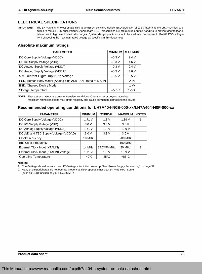
32-Bit System-on-Chip LH7A404
Product data sheet 29
NXP Semiconductors
ELECTRICAL SPECIFICATIONSIMPORTANT: The LH7A404 is an electrostatic discharge (ESD) sensitive device. ESD protection circuitry internal to the LH7A404 has been
added to reduce ESD susceptibility. Appropriate ESD precautions are still required during handling to prevent degradation orfailure due to high electrostatic discharges. System design practices should be evaluated to prevent LH7A404 ESD voltagesfrom exceeding the maximum rated voltage as specified in this data sheet.
Absolute maximum ratings
NOTE: These stress ratings are only for transient conditions. Operation at or beyond absolute maximum rating conditions may affect reliability and cause permanent damage to the device.
Recommended operating conditions for LH7A404-N0E-000-xx/LH7A404-N0F-000-xx
NOTES:1. Core Voltage should never exceed I/O Voltage after initial power up. See “Power Supply Sequencing” on page 31.2. Many of the peripherals do not operate properly at clock speeds other than 14.7456 MHz. Some
(such as USB) function only at 14.7456 MHz.
PARAMETER MINIMUM MAXIMUM
DC Core Supply Voltage (VDDC) 0.3 V 2.4 V
DC I/O Supply Voltage (VDD) 0.3 V 4.6 V
DC Analog Supply Voltage (VDDA) 0.3 V 2.4 V
DC Analog Supply Voltage (VDDAD) 0.3 V 4.6 V
5 V Tolerant Digital Input Pin Voltage 0.5 V 5.5 V
ESD, Human Body Model (Analog pins AN0 - AN9 rated at 500 V) 2 kV
ESD, Charged Device Model 1 kV
Storage Temperature 55°C 125°C
PARAMETER MINIMUM TYPICAL MAXIMUM NOTES
DC Core Supply Voltage (VDDC) 1.71 V 1.8 V 1.89 V 1
DC I/O Supply Voltage (VDD) 3.0 V 3.3 V 3.6 V
DC Analog Supply Voltage (VDDA) 1.71 V 1.8 V 1.89 V
DC A/D and TSC Supply Voltage (VDDAD) 3.0 V 3.3 V 3.6 V
Clock Frequency 10 MHz 200 MHz
Bus Clock Frequency 100 MHz
External Clock Input (XTALIN) 14 MHz 14.7456 MHz 20 MHz 2
External Clock Input (XTALIN) Voltage 1.71 V 1.8 V 1.89 V
Operating Temperature 40°C 25°C +85°C
This Manual:http://www.manuallib.com/nxp/lh7a404-n-system-on-chip-datasheet.html

LH7A404 32-Bit System-on-Chip
30 Product data sheet
NXP Semiconductors
Recommended Operating Conditions for LH7A404-N0E-092-xx/LH7A404-N0F-092-xx
NOTES:1. Core Voltage should never exceed I/O Voltage after initial power up. See “Power Supply Sequencing” on page 31.2. Many blocks do not operate properly at speeds other than 14.7456 MHz. Some (such as USB) function only at 14.7456 MHz.
NOTE: *LH7A404-N0E-000-xx and LH7A404-N0F-000-xx only. Table 8 is representative of a typical device. Guaranteed values are in the Recommended Operating Conditions table.
PARAMETER MINIMUM TYPICAL MAXIMUM NOTES
DC Core Supply Voltage (VDDC) 2.0 V 2.1 V 2.2 V 1
DC I/O Supply Voltage (VDD) 3.14 V 3.3 V 3.6 V
DC Analog Supply Voltage (VDDA) 2.0 V 2.1 V 2.2 V
DC A/D and TSC Supply Voltage (VDDAD) 3.0 V 3.3 V 3.6 V
Clock Frequency 10 MHz 266 MHz
Bus Clock Frequency 133 MHz
External Clock Input (XTALIN) 14 MHz 14.7456 MHz 20 MHz 2
External Clock Input (XTALIN) Voltage 1.71 V 1.8 V 1.89 V
Operating Temperature 40°C 25°C +85°C
Table 8. Clock Frequency vs. Voltages (VDD) vs. Temperature*
PARAMETER 1.71 V 1.80 V 1.89 V
25°CClock Frequency (FCLK) 213 MHz 227 MHz 253 MHz
Clock Period (1/FCLK) 4.69 ns 4.41 ns 3.95 ns
70°CClock Frequency (FCLK) 205 MHz 220 MHz 236 MHz
Clock Period (1/FCLK) 4.88 ns 4.46 ns 2.36 ns
85°CClock Frequency (FCLK) 200 MHz 212 MHz 232 MHz
Clock Period (1/FCLK) 5.00 ns 4.72 ns 4.24 ns
Figure 5. Temperature/Voltage/Speed Chart (LH7A404-N0E-000-xx and LH7A404-N0F-000-xx Only)
LH7A404-182
FR
EQ
UE
NC
Y (
MH
z)
250
255
245
240
235
230
225
220
215
210
205
20025 35 45 55
TEMP (°C)
65 75 85
1.89 V (+5%)
1.80 V
1.71 V (-5%)
This Manual:http://www.manuallib.com/nxp/lh7a404-n-system-on-chip-datasheet.html
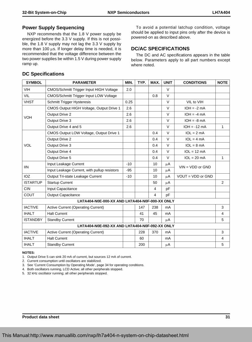
32-Bit System-on-Chip LH7A404
Product data sheet 31
NXP Semiconductors
Power Supply SequencingNXP recommends that the 1.8 V power supply be
energized before the 3.3 V supply. If this is not possi-ble, the 1.8 V supply may not lag the 3.3 V supply bymore than 100 s. If longer delay time is needed, it isrecommended that the voltage difference between thetwo power supplies be within 1.5 V during power supplyramp up.
To avoid a potential latchup condition, voltageshould be applied to input pins only after the device ispowered-on as described above.
DC/AC SPECIFICATIONS The DC and AC specifications appears in the table
below. Parameters apply to all part numbers exceptwhere noted.
DC Specifications
NOTES:1. Output Drive 5 can sink 20 mA of current, but sources 12 mA of current.2. Current consumption until oscillators are stabilized.3. See ’Current Consumption by Operating Mode’, page 34 for operating conditions.4. Both oscillators running, LCD Active; all other peripherals stopped.5. 32 kHz oscillator running; all other peripherals stopped.
SYMBOL PARAMETER MIN. TYP. MAX. UNIT CONDITIONS NOTE
VIH CMOS/Schmitt Trigger Input HIGH Voltage 2.0 V
VIL CMOS/Schmitt Trigger Input LOW Voltage 0.8 V
VHST Schmitt Trigger Hysteresis 0.25 V VIL to VIH
VOH
CMOS Output HIGH Voltage, Output Drive 1 2.6 V IOH = -2 mA
Output Drive 2 2.6 V IOH = -4 mA
Output Drive 3 2.6 V IOH = -8 mA
Output Drive 4 and 5 2.6 V IOH = -12 mA 1
VOL
CMOS Output LOW Voltage, Output Drive 1 0.4 V IOL = 2 mA
Output Drive 2 0.4 V IOL = 4 mA
Output Drive 3 0.4 V IOL = 8 mA
Output Drive 4 0.4 V IOL = 12 mA
Output Drive 5 0.4 V IOL = 20 mA 1
IINInput Leakage Current -10 10 A
VIN = VDD or GNDInput Leakage Current, with pullup resistors -95 10 A
IOZ Output Tri-state Leakage Current -10 10 A VOUT = VDD or GND
ISTARTUP Startup Current 50 A 2
CIN Input Capacitance 4 pF
COUT Output Capacitance 4 pF
LH7A404-N0E-000-XX AND LH7A404-N0F-000-XX ONLY
IACTIVE Active Current (Operating Current) 147 238 mA 3
IHALT Halt Current 41 45 mA 4
ISTANDBY Standby Current 70 A 5
LH7A404-N0E-092-XX AND LH7A404-N0F-092-XX ONLY
IACTIVE Active Current (Operating Current) 228 370 mA 3
IHALT Halt Current 60 mA 4
IHALT Standby Current 200 A 5
This Manual:http://www.manuallib.com/nxp/lh7a404-n-system-on-chip-datasheet.html

LH7A404 32-Bit System-on-Chip
32 Product data sheet
NXP Semiconductors
Analog-To-Digital Converter Electrical Characteristics
Table 9 shows the derated specifications forextended temperature operation. See Figure 6 for theADC transfer characteristics.
NOTES:1. The analog section of the ADC takes 16 × A2DCLK cycles per conversion,
plus 1 × A2DCLK cycles to be made available in the PCLK domain. An additional 3 × PCLK cycles are required before being available on the APB.
2. Data out = 0000000000 when the analog input equals the negative reference. Data out = 1111111111 when the analog input equals the positive reference.
3. Guaranteed monotonic.4. INL calculated as deviation from ‘best fit’ line after subtracting offset/gain errors over the center
90 % of full scale output range.5. DC voltage error for the transition voltage from code 511 (0x1FF) to 512 (0x200)6. The internal voltage reference is driven to nominal value VREF = 2.0 V. Using the Reference Multiplexer,
alternative low impedance (RS < 500) voltages can be selected as reference voltages. The range of voltages allowed are specified above.
7. The analog input pins can be driven anywhere between the power supply rails. If the voltage at the input to the ADC exceeds VREF+ or is below VREF-, the A/D result will saturate appropriately at positive or negative full scale. Trying to pull the analog input pins above or below the power supply rails will cause protection diodes to be forward-biased, resulting in large current source/sink and possible damage to the ADC.
8. Bandgap and other low-bandwidth circuitry operating. All other ADC blocks shut down.
Table 9. ADC Electrical Characteristics
PARAMETER MIN. TYP. MAX. UNITS NOTES
A/D Resolution 10 10 Bits
Throughput Conversion 17 CLK Cycles 1
Acquisition Time 3 CLK Cycles
Data Format binary 2
Clk Frequency 500 5,000 ns
Differential Non-Linearity (DNL) -0.99 +4.5 LSB 3
Integral Non-Linearity (INL) -4.5 +4.5 LSB 4
Offset Error +35 +50 mV 5
Gain Error -4.0 4.0 LSB
Reference Voltage Output 1.85 2.0 2.15 V
VREF- VSSA VSSA (VREF+) -1.0 V 6
VREF+ (VREF-) +1.0 VREF VDDAD V 6
Crosstalk between channels -60 dB
Analog Input Voltage Range 0 VDDAD V 7
Analog Input Current 5 A
Reference Input Current 5 A
Analog Input capacitance 15 pF
Operating Supply Voltage 3.0 3.6 V
Operating Current, VDDAD 590 1000 A
Standby Current, VDDAD 180 A 8
Stop Current, VDDAD 1 A
Brownout Trip Point (falling point) 2.36 2.63 2.9 V
Brownout Hysteresis 120 mV
Operating Temperature 40 85 °C
This Manual:http://www.manuallib.com/nxp/lh7a404-n-system-on-chip-datasheet.html

32-Bit System-on-Chip LH7A404
Product data sheet 33
NXP Semiconductors
AC Test Conditions
Figure 6. ADC Transfer Characteristics
PARAMETER RATING UNIT
DC I/O Supply Voltage (VDD) 3.0 to 3.6 V
DC Core Supply Voltage (VDDC) 1.7 to 1.9 V
Input Pulse Levels VSS to 3 V
Input Rise and Fall Times 2 ns
Input and Output Timing Reference Levels VDD/2 V
1015
1
2
3
4
5
6
7
8
9
1018
1019
1020
1021
1022
1023
1024
1016 1017 1018 1019
LH7A404-154
1020 1021 1022 1023 10241 2 3 4 5 6 7 8 9
INTEGRALNON-LINEARITY
ACTUALTRANSFER CURVE
IDEALTRANSFER CURVE
CENTER OF ASTEP OF THE ACTUAL
TRANSFER CURVE
OFFSETERROR
OFFSETERROR
LSB
DNL
GAINERROR
This Manual:http://www.manuallib.com/nxp/lh7a404-n-system-on-chip-datasheet.html

LH7A404 32-Bit System-on-Chip
34 Product data sheet
NXP Semiconductors
CURRENT CONSUMPTION BY OPERATING MODECurrent consumption can depend on a number
of parameters. To make these data more usable, thevalues presented in Table 11 were derived under theconditions described here.
Maximum Specified Value
The values specified in the MAXIMUM column weredetermined using these operating characteristics:
• All IP blocks either operating or enabled at maximumfrequency and size configuration
• Core operating at maximum power configuration
• All voltages at maximum specified values
• Nominal specified ambient temperature.
Typical
The values in the TYPICAL column were determinedusing a ‘typical’ application under ‘typical’ environmentalconditions and the following operating characteristics:
• LINUX operating system running from SDRAM
• UART and AC97 peripherals operating; all otherperipherals as needed by the OS
• LCD enabled with 320 × 240 × 16-bit color, 60 Hzrefresh rate, data in SDRAM
• I/O loads at nominal
• Cache enabled
• FCLK = 200; HCLK = 100; PCLK = 50 MHz
• All voltages at typical values
• Nominal case temperature.
PERIPHERAL CURRENT CONSUMPTIONIn addition to the modal current consumption, Table
10 shows the typical current consumption for eachof the on-board peripheral blocks. The values weredetermined with the peripheral clock running at 200MHz, typical conditions, and no I/O loads. This currentis supplied by the 1.8 V power supply.
NOTES:1. FCLK = 200 MHZ pertains to LH7A404-N0E-000-xx and LH7A404-N0F-000-xx2. FCLK = 266 MHz pertains to LH7A404-N0E-092-xx and LH7A404-N0F-092-xx.
Table 10. Peripheral Current Consumption
PERIPHERAL TYPICAL UNITS
AC97 1.3 mA
UART (each) 1.0 mA
RTC 0.005 mA
Timers (each) 0.1 mA
LCD (+I/O) 5.4 (+1.0) mA
MMC 0.6 mA
SCI 23 mA
PWM (each) 45 A
BMI-SWI 1.0 mA
BMI-SBus 1.0 mA
SDRAM (+I/O) 1.5 (+14.8) mA
USB Device (+PLL) 5.6 (+3.3) mA
ACI 0.8 mA
VIC 610 A
KMI 38 A
USB Host 715 A
ADC/TSC 590 A
Table 11. Current Consumption by Mode
SYMBOL PARAMETER FCLK = 200 MHz (TYP.) FCLK = 266 MHz (TYP.) UNITS
RUN MODE
ICORE Core Current 132 199 mA
IIO I/O Current 15 29 mA
HALT MODE (All Peripherals Disabled)
ICORE Core Current 40 58 mA
IIO I/O Current 1 2 mA
STANDBY MODE (Typical Conditions Only)
ICORE Core Current 66 200 A
IIO I/O Current 4 4 A
This Manual:http://www.manuallib.com/nxp/lh7a404-n-system-on-chip-datasheet.html

32-Bit System-on-Chip LH7A404
Product data sheet 35
NXP Semiconductors
AC Specifications All signals described in Table 12 relate to transi-
tions following an internal reference clock signal.The illustration in Figure 7 represents all cases ofthese sets of measurement parameters.
The reference clock signals in this design are:
• HCLK, internal System Bus clock (‘C’ in timing data)
• PCLK, the Peripheral Bus clock
• SSPCLK, the Synchronous Serial Port clock
• UARTCLK, the UART Interface clock
• LCDDCLK, the LCD Data clock from the LCD Controller
• ACBITCLK, the AC97 and ACI clock
• SCLK, the Synchronous Memory clock.
All signal transitions are measured from the 50 %point of the clock to the 50 % point of the signal.
For outputs from the LH7A404, tOVXXX (e.g. tOVA)represents the amount of time for the output to becomevalid from the rising edge of the reference clock signal.Maximum requirements for tOVXXX are shown inTable 12.
The signal tOHXXX (e.g. tOHA) represents theamount of time the output must be held valid after therising edge of the reference clock signal. Minimumrequirements for tOHXXX are listed in Table 12.
For inputs, tISXXX (e.g. tISD) represents theamount of setup time the input signal must be valid aftera valid address bus, or rising edge of the peripheralclock. Maximum requirements for tISXXX are shown inTable 12.
The signal tIHXXX (e.g. tIHD) represents theamount of time the output must be held valid followingthe rising edge of the reference clock signal. Minimumrequirements are shown in Table 12.
Figure 7. LH7A404 Signal Timing
REFERENCECLOCK
OUTPUTSIGNAL (O)
INPUTSIGNAL (I)
tOVXXX tOHXXX
tISXXX tIHXXX
LH7A404-9
This Manual:http://www.manuallib.com/nxp/lh7a404-n-system-on-chip-datasheet.html

LH7A404 32-Bit System-on-Chip
36 Product data sheet
NXP Semiconductors
Table 12. AC Signal Characteristics
SIGNAL TYPE LOAD SYMBOL MIN. MAX. DESCRIPTION NOTES
ASYNCHRONOUS MEMORY INTERFACE SIGNALS (+ [wait states × HCLK period])
A[27:0]
Output 50 pF tRC 4 × tHCLK – 7.0 ns 4 × tHCLK + 7.5 ns Read Cycle Time 1
Output 50 pF tWC 4 × tHCLK – 7.0 ns 4 × tHCLK + 7.5 ns Write Cycle Time 1
— — tWS tHCLK ns tHCLK ns Wait State Width 1
D[31:0]
Output 50 pF
tDVWE tHCLK – 6.0 ns tHCLK – 2.0 ns Data Valid to Write Edge (nWE invalid) 1
tDHWE tHCLK – 7.0 ns tHCLK + 2.0 ns Data Hold after Write Edge (nWE invalid) 1
tDVBE tHCLK – 5.0 ns tHCLK – 1.0 ns Data Valid to nBLE Invalid 1
tDHBE tHCLK – 7.0 ns tHCLK + 3.0 ns Data Hold after nBLE Invalid 1
Input —
tDSCS 15 ns — Data Setup to nCSx Invalid 1
tDHCS 0 ns — Data Hold to nCSx Invalid 1
tDSOE 15 ns — Data Setup to nOE Invalid 1
tDHOE 0 ns — Data Hold to nOE Invalid 1
tDSBE 15 ns — Data Setup to nBLE Invalid 1
tDHBE 0 ns — Data Hold to nBLE Invalid 1
nCS[7:0] Output 50 pF
tCS 2 × tHCLK – 3.0 ns 2 × tHCLK + 3.0 ns nCSx Width 1
tAVCS tHCLK – 4.0 ns tHCLK Address Valid to nCSx Valid 1
tAHCS tHCLK tHCLK + 4.5 ns Address Hold after nCSx Invalid 1
nWE Output 50 pF
tWE tHCLK – 2.0 ns tHCLK + 1.0 ns nWE Width 1
tAVWE tHCLK – 4.0 ns tHCLK ns Address Valid to nWE Valid 1
tCSHWE tHCLK – 1.0 ns tHCLK + 2.0 ns nCSx Hold after nWE Invalid 1
nOE Output 50 pF
tOE 2 × tHCLK – 3.0 ns 2 × tHCLK + 3.0 ns nOE Width 1
tAVOE tHCLK – 4.0 ns tHCLK Address Valid to nOE Valid 1
tAHOE tHCLK tHCLK + 4.5 ns Address Hold after nOE Invalid 1
nBLE (Write) Output 50 pF
tBEW tHCLK – 5.0 ns tHCLK nBLE Width 1
tAVBE tHCLK – 2.0 ns tHCLK Address Valid to nBLE Valid 1
tCSHBE tHCLK tHCLK + 3.0 ns nCSx Hold after nBLE Invalid 1
nBLE (Read) Output 50 pF
tBER 2 × tHCLK – 5.0 ns 2 × tHCLK + 3.0 ns nBLE Width 1
tAVBE tHCLK – 2.0 ns tHCLK Address Valid to nBLE Valid 1
tAHBE tHCLK tHCLK + 4.5 ns Address Hold after nBLE Invalid 1
SYNCHRONOUS MEMORY INTERFACE SIGNALS (‘-092’ parts/’-000’ parts)
SA[13:0] Output 50 pFtOVA — 5.5/7.5 ns Address Valid 2
tOHA 1.5/1.5 ns — Address Hold 2
A[17:16]/SB[1:0]
Output 50 pF tOVB — 5.5/7.5 ns Bank Select Valid 2
D[31:0]
Output 50 pFtOHD 1.5ns — Data Hold 2
tOVD 2 ns 5.5/7.5 ns Data Valid 2
Input —tISD 1.5/2.5 ns — Data Setup 2
tIHD 1.0/1.5 ns — Data Hold 2
nCAS Output 50 pFtOVCA 2 ns 5.5/7.5 ns CAS Valid 2
tOHCA 1.5/2 ns — CAS Hold 2
nRAS Output 50 pFtOVRA 2 ns 5.5/7.5 ns RAS Valid 2
tOHRA 1.5/2 ns — RAS Hold 2
nSWE Output 50 pFtOVSDW 2 ns 5.5/7.5 ns Write Enable Valid 2
tOHSDW 1.5/2 ns — Write Enable Hold 2
SCKE[1:0] Output 50 pF tOVC0 2 ns 5.5/7.5 ns Clock Enable Valid 2
DQM[3:0] Output 50 pF tOVDQ 2 ns 5.5/7.5 ns Data Mask Valid 2
nSCS[3:0] Output 50 pFtOVSC 2 ns 5.5/7.5 ns Synchronous Chip Select Valid 2
tOHSC 1.5/2 ns — Synchronous Chip Select Hold 2
PCMCIA INTERFACE SIGNALS (+ [wait states × HCLK period])
nPCREG Output 50 pFtOVDREG — tHCLK + 5 ns nREG Valid
tOHDREG 4 × tHCLK – 5 ns — nREG Hold
This Manual:http://www.manuallib.com/nxp/lh7a404-n-system-on-chip-datasheet.html

32-Bit System-on-Chip LH7A404
Product data sheet 37
NXP Semiconductors
NOTES:1. Register BCRx:WST1 = 0b0002. The ‘x/x’ in the MIN./MAX. indicates (LH7A404-N0E-092-xx and H7A404-N0F-092-xx)/
(LH7A404-N0E-000-xx and LH7A404-N0F-000-xx), respectively.3. ‘tcyc’ is the period of one MMC Clock4. ‘tcyc’ is the period of one AC97 Clock 5. ‘nC’ in the MIN./MAX. columns indicates the number of system clock (HCLK) periods after valid address6. For Output Drive strength specifications, refer to Table 2
D[31:0]
Output 50 pFtOVD — tHCLK + 5 ns Data Valid
tOHD 4 × tHCLK – 6 ns — Data Hold
Input —tISD — tHCLK - 10 ns Data Setup Time
tIHD 4 × tHCLK – 5 ns — Data Hold Time
nPCCE1 Output 50 pFtOVCE1 — tHCLK + 5 ns Chip Enable 1 Valid
tOHCE1 4 × tHCLK – 5 ns — Chip Enable 1 Hold
nPCCE2 Output 50 pFtOVCE2 — tHCLK + 5 ns Chip Enable 2 Valid
tOHCE2 4 × tHCLK – 5 ns — Chip Enable 2 Hold
nPCOE Output 50 pFtOVOE — tHCLK + 5 ns Output Enable Valid
tOHOE 3 × tHCLK – 5 ns — Output Enable Hold
nPCWE Output 50 pFtOVWE — n × tHCLK + 5 ns Write Enable Valid
tOHWE 3 × tHCLK – 5 ns — Write Enable Hold
PCDIR Output 50 pFtOVPCD — tHCLK + 5 ns Card Direction Valid
tOHPCD 4 × tHCLK – 5 ns — Card Direction Hold
MMC INTERFACE SIGNALS
MMCCMD Output 50 pFtOVCMD — ½tcyc – 3 ns MMC Command Valid 3
tOHCMD ½tcyc + 3 ns — MMC Command Hold 3
MMCDATA Output 50 pFtOVDAT — ½tcyc – 3 ns MMC Data Valid 3
tOHDAT ½tcyc + 3 ns — MMC Data Hold 3
MMCDATA Input —tISDAT 5 ns — MMC Data Setup
tIHDAT 5 ns — MMC Data Hold
MMCCMD Input —tISCMD 5 ns — MMC Command Setup
tIHCMD 5 ns — MMC Command Hold
AC97 INTERFACE SIGNALS
ACOUT Output 50 pFtOVAC97 — ½tcyc – 10 ns AC97 Output Valid 4
tOHAC97 ½tcyc + 10 ns — AC97 Output Hold 4
ACIN Input —tISAC97 2.5 ns — AC97 Input Setup
tIHAC97 2.5 ns — AC97 Input Hold
ACSYNC Output 50 pFtOVAC97 — ½tcyc – 10 ns AC97 Synchronization Valid 4
tOHAC97 ½tcyc + 10 ns — AC97 Synchronization Hold 4
SYNCHRONOUS SERIAL PORT (SSP)
SSPFRM Output 50 pFtOVFRM — 10 ns SSP Frame Output Valid
tOHFRM 5 ns — SSP Frame Output Hold
SSPTX Output 50 pFtOVTX 10 ns SSP Transmit Valid
tOHTX 5 ns — SSP Transmit Hold
SSPRX Input —tISRX 14 ns — SSP Receive Setup
tIHRX 14 ns — SSP Receive Hold
SSPCLK Output 50 pF tCLK 8.819 ms 271 ns SSP Clock Period
AUDIO CODEC INTERFACE (ACI)
ACOUT Output 50 pFtOVD — 15 ns ACOUT delay from rising clock edge
tOHD 10 ns — ACOUT Hold
ACIN InputtIS 10 ns — ACIN Setup
tIH 2.5 ns — ACIN Hold
COLOR LCD CONTROLLER
LCDVD [17:0] Output 50 pF tOV — 3 ns LCD Data Clock to Data Valid
Table 12. AC Signal Characteristics (Cont’d)
SIGNAL TYPE LOAD SYMBOL MIN. MAX. DESCRIPTION NOTES
This Manual:http://www.manuallib.com/nxp/lh7a404-n-system-on-chip-datasheet.html

LH7A404 32-Bit System-on-Chip
38 Product data sheet
NXP Semiconductors
SMC WaveformsFigure 8 and Figure 9 show waveforms and timing
for an external asynchronous memory Write. Figure 10and Figure 11 show the waveforms and timing for anexternal asynchronous memory Read.
Figure 8. External Asynchronous Memory Write, Zero Wait States (BCRx:WST1 = 0b000)
HCLK
A[27:0]
tWC
VALID ADDRESS
VALID DATA
tDVWE,tDVBE
tDHWE,tDHBE
LH7A404-10
0 1 2 3 4
tCS
nCS Valid
nWE Valid
nBLE Valid
tAVCS tAHCS
tWE tCSHWEtAVWE
tBEW tCSHBEtAVBE
D[31:0]
nCSx
nWE
nBLE
WRITE EDGE
This Manual:http://www.manuallib.com/nxp/lh7a404-n-system-on-chip-datasheet.html

32-Bit System-on-Chip LH7A404
Product data sheet 39
NXP Semiconductors
Figure 9. External Asynchronous Memory Write, Four Wait States (BCRx:WST1 = 0b100)
LH7A404-189
A[27:0]
HCLK
0 WAIT STATE
WAITSTATE 1
WAITSTATE 2
WAITSTATE 3
WAITSTATE 4
D[31:0]
nCSx
nWE
nBLE
WRITE EDGE
876543210
nCSx Valid
nWE Valid
nBLE Valid
tWS tWS tWS tWS
VALID ADDRESS
VALID DATA
This Manual:http://www.manuallib.com/nxp/lh7a404-n-system-on-chip-datasheet.html
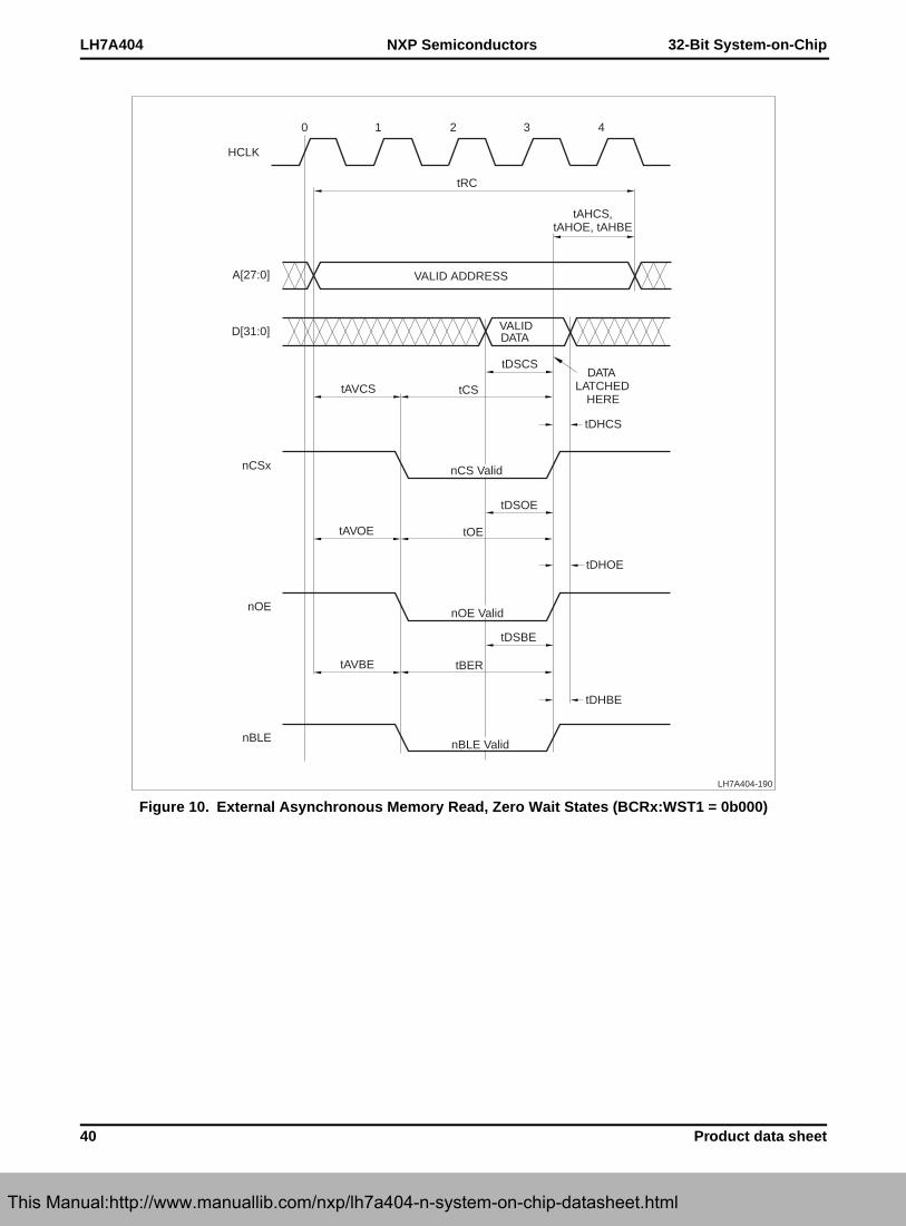
LH7A404 32-Bit System-on-Chip
40 Product data sheet
NXP Semiconductors
Figure 10. External Asynchronous Memory Read, Zero Wait States (BCRx:WST1 = 0b000)
HCLK
A[27:0]
tRC
tAHCS,tAHOE, tAHBE
tDHCS
tDHBE
tDHOE
VALIDDATA
VALID ADDRESS
DATALATCHED
HERE
LH7A404-190
0 1 2 3 4
tAVCS
tDSCS
tDSBE
tCS
tBER
tDSOE
tOEtAVOE
tAVBE
D[31:0]
nCSx
nOE
nBLE
nCS Valid
nOE Valid
nBLE Valid
This Manual:http://www.manuallib.com/nxp/lh7a404-n-system-on-chip-datasheet.html

32-Bit System-on-Chip LH7A404
Product data sheet 41
NXP Semiconductors
Figure 11. External Asynchronous Memory Read, Four Wait States (BCRx:WST1 = 0b100)
LH7A404-12
109876543210
A[27:0]
HCLK
VALID ADDRESS
D[31:0]
nCS[3:0,CS[7:6]
nOE
VALID DATA
nBLE
0 WAIT STATE,DATA WOULD BELATCHED HERE tWS
4 WAIT STATES,DATA LATCHED
HERE
WAITSTATE 1
WAITSTATE 2
WAITSTATE 3
WAITSTATE 4
nCSx Valid
nOE Valid
nBLE Valid
tWS tWS tWS
This Manual:http://www.manuallib.com/nxp/lh7a404-n-system-on-chip-datasheet.html

LH7A404 32-Bit System-on-Chip
42 Product data sheet
NXP Semiconductors
TIMING FOR nWAIT SIGNALLINGIn addition to being able to program the number of
Wait States, the SMC also can use nWAIT signalling toextend transactions. When the nWAIT input is asserted,the current transaction is held in suspense until nWAIT
is released, allowing slow memory or memory-mappedperipherals time to complete the action.
Figure 12 through Figure 17 illustrate nWAITtiming using different WST register settings andcircumstances.
NOTES:1. The timing relationship is specified as a cycle-based timing.
Variations caused by clock jitter, power rail noise, and I/O cond-tioning will cause these timings to vary nominally. It is recom-mended that designers add a small margin to avoid possiblecorner-case conditions.
2. The Bank Configuration Register (BCRx:WST1) must have ReadWait States set to a minimum of 2.
3. The number of HCLK periods that nWAIT lags assertion of nCSxmust be added to the minimum value for BCRx:WST1. For exam-ple, if nWAIT lags nCSx by 3 HCLK periods, the minimum settingof BCRx:WST1 is 2 + 3, or a total of 5 as the minimum value forBCRx:WST1.
4. No nWAIT delay cycles are added for any nWAIT assertions thatoccur prior to the beginning of the WSD-2 delay. These nWAITassertions are ignored.
5. Once the WSD-2 delay begins, one HCLK cycle is added to thetransaction each time nWAIT is sampled and queued (SQ-x). ThenWAIT cycles begin being added after the Wait State Countdownreaches WSD-0.
6. Once nWAIT is sampled HIGH (de-asserted), the current memorytransaction is queued to complete.
7. Since static and dynamic memory cannot be accessed at thesame time, prolonged extension of an SMC transaction by eitherWait States or nWAIT delays can cause refresh failure for theSDRAM, and may cause SDRAM data loss.
Figure 12. nWAIT Read Sequence (BCRx:WST1 = 2); Minimum Wait State Example
PARAMETER DESCRIPTION MIN. MAX. UNIT 1
tDA_nCS(x)_nWAIT Delay from nCS(x) assertion to nWAIT assertion 0 29 HCLK periods
tDD_nWAIT_nCS(x) Delay from nWAIT deassertion to nCS(x) deassertion 4 HCLK periods
tDD_nWAIT_nOE Delay from nWAIT deassertion to nOE deassertion 4 HCLK periods
tA_nWAIT Assertion time of nWAIT 2 HCLK periods
tDA_nCS(x)_nWAIT
HCLK
nCS(x)
nOE
nWAIT
NOTES:SQ: nWAIT Sampled and QueuedSI: nWAIT Sampled and Ignored
tA_nWAIT
SQ-4 SQ-3 SQ-2 SQ-1 SQ-0
tDD_nWAIT_nCS(x)
tDD_nWAIT_nOE
LH7A404-203
WSD-2DELAY
WSD-1DELAY
WSD-0DELAY
SQ-4nWAITDELAY
SQ-3nWAITDELAY
SQ-2nWAITDELAY
SQ-1nWAITDELAY
SQ-0nWAITDELAY
ENDCYCLE
TransactionSequence
This Manual:http://www.manuallib.com/nxp/lh7a404-n-system-on-chip-datasheet.html

32-Bit System-on-Chip LH7A404
Product data sheet 43
NXP Semiconductors
Figure 13. nWAIT Read Sequence (BCRx:WST1 = 4); Ignored and Queued nWAIT Delays
Figure 14. nWAIT Read Sequence (BCRx:WST1 = 4); nWAIT Has No Effect On Current Transaction
WSD-4DELAY
WSD-3DELAY
WSD-2DELAY
WSD-1DELAY
WSD-0DELAY
SQ-4nWAITDELAY
SQ-3nWAITDELAY
SQ-2nWAITDELAY
SQ-1nWAITDELAY
SQ-0nWAITDELAY
ENDCYCLE
tDD_nWAIT_nCS(x)
tDD_nWAIT_nOE)
tA_nWAIT
SI SI SQ-4 SQ-3 SQ-2 SQ-1 SQ-0
nCS(x)
nOE
nWAIT
HCLK
TransactionSequence
NOTES:SQ: nWAIT Sampled and QueuedSI: nWAIT Sampled and Ignored
tDA_nCS(x)_nWAIT
LH7A404-204
WSD-4DELAY
WSD-3DELAY
WSD-2DELAY
WSD-1DELAY
WSD-0DELAY
ENDCYCLE
SI SI
nCS(x)
HCLK
nOE
nWAIT
TransactionSequence
NOTES:SQ: nWAIT Sampled and QueuedSI: nWAIT Sampled and Ignored
LH7A404-205
tDA_nCS(x)_nWAIT
tA_nWAIT
This Manual:http://www.manuallib.com/nxp/lh7a404-n-system-on-chip-datasheet.html

LH7A404 32-Bit System-on-Chip
44 Product data sheet
NXP Semiconductors
NOTES:1. The timing relationship is specified as a cycle-based timing. Variations caused by clock jitter,
power rail noise, and I/O condtioning will cause these timings to vary nominally. It is recommended that designers add a small margin to avoid possible corner-case conditions.
2. The Bank Configuration Register (BCRx:WST1) must have Write Wait States set to a minimum of 2.3. The number of HCLK periods that nWAIT lags assertion of nCSx must be added to the minimum value
for BCRx:WST1. For example, if nWAIT lags nCSx by 3 HCLK periods, the minimum setting of BCRx:WST1 is 2 + 3, or a total of 5 as the minimum value for BCRx:WST1.
4. No nWAIT delay cycles are added for any nWAIT assertions that occur prior to the beginning of the WSD-2 delay. These nWAIT assertions are ignored.
5. Once the WSD-2 delay begins, one HCLK cycle is added to the transaction each time nWAIT is sampled and queued (SQ-x). The nWAIT cycles begin being added after the Wait State Countdown reaches WSD-0.
6. Once nWAIT is sampled HIGH (de-asserted), the current memory transaction is queued to complete.7. Since static and dynamic memory cannot be accessed at the same time, prolonged extension of
an SMC transaction by either Wait States or nWAIT delays can cause refresh failure for the SDRAM, and may cause SDRAM data loss.
Figure 15. nWAIT Write Sequence (BCRx:WST1 = 2); Minimum Wait State Example
PARAMETER DESCRIPTION MIN. MAX. UNIT1
tIDA_nCS(x)_nWAIT Delay from nCS(x) assertion to nWAIT assertion 0 29 HCLK periods
tDD_nWAIT_nCS(x) Delay from nWAIT deassertion to nCS(x) deassertion 4 HCLK periods
tDD_nWAIT_nWE Delay from nWAIT deassertion to nWE deassertion 3 HCLK periods
tA_nWAIT Assertion time of nWAIT 2 HCLK periods
tDA_nCS(x)_nWAIT
HCLK
nCS(x)
nWE
nWAIT
NOTES:SQ: nWAIT Sampled and QueuedSI: nWAIT Sampled and Ignored
tA_nWAIT
SQ-4 SQ-3 SQ-2 SQ-1 SQ-0
tDD_nWAIT_nCS(x)
tDD_nWAIT_nWE
LH7A404-206
WSD-2DELAY
WSD-1DELAY
WSD-0DELAY
SQ-4nWAITDELAY
SQ-3nWAITDELAY
SQ-2nWAITDELAY
SQ-1nWAITDELAY
SQ-0nWAITDELAY
ENDCYCLE
TransactionSequence
This Manual:http://www.manuallib.com/nxp/lh7a404-n-system-on-chip-datasheet.html
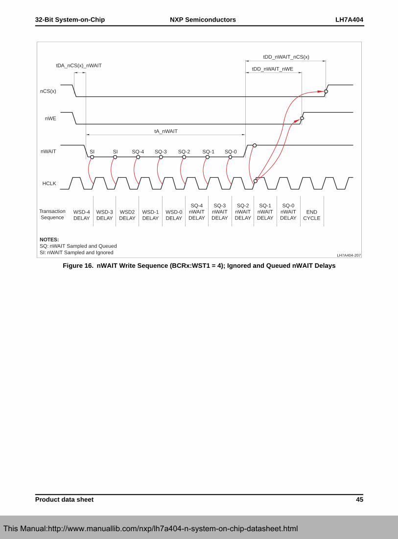
32-Bit System-on-Chip LH7A404
Product data sheet 45
NXP Semiconductors
Figure 16. nWAIT Write Sequence (BCRx:WST1 = 4); Ignored and Queued nWAIT Delays
WSD-4DELAY
WSD-3DELAY
WSD2DELAY
WSD-1DELAY
WSD-0DELAY
SQ-4nWAITDELAY
SQ-3nWAITDELAY
SQ-2nWAITDELAY
SQ-1nWAITDELAY
SQ-0nWAITDELAY
ENDCYCLE
tDD_nWAIT_nCS(x)
tDD_nWAIT_nWE
tA_nWAIT
SI SI SQ-4 SQ-3 SQ-2 SQ-1 SQ-0
nCS(x)
nWE
nWAIT
HCLK
TransactionSequence
NOTES:SQ: nWAIT Sampled and QueuedSI: nWAIT Sampled and Ignored
tDA_nCS(x)_nWAIT
LH7A404-207
This Manual:http://www.manuallib.com/nxp/lh7a404-n-system-on-chip-datasheet.html

LH7A404 32-Bit System-on-Chip
46 Product data sheet
NXP Semiconductors
Figure 17. nWAIT Write Sequence (BCRx:WST1 = 4); nWAIT Has No Effect On Current Transaction
WSD-4DELAY
WSD-3DELAY
WSD-2DELAY
WSD-1DELAY
WSD-0DELAY
ENDCYCLE
SI SI
nCS(x)
HCLK
nWE
nWAIT
TransactionSequence
NOTES:SQ: nWAIT Sampled and QueuedSI: nWAIT Sampled and Ignored
LH7A404-208
tDA_nCS(x)_nWAIT
tA_nWAIT
This Manual:http://www.manuallib.com/nxp/lh7a404-n-system-on-chip-datasheet.html
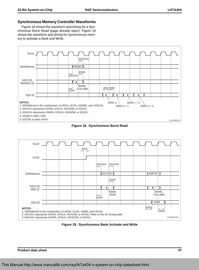
32-Bit System-on-Chip LH7A404
Product data sheet 47
NXP Semiconductors
Synchronous Memory Controller WaveformsFigure 18 shows the waveform and timing for a Syn-
chronous Burst Read (page already open). Figure 19shows the waveform and timing for synchronous mem-ory to activate a bank and Write.
Figure 18. Synchronous Burst Read
Figure 19. Synchronous Bank Activate and Write
LH7A404-13
SA[13:0],SBANK[1:0]
D[31:0]
NOTES: 1. SDRAMcmd is the combination of nRAS, nCAS, nSDWE, and nSDCSx.2. tOVXXX represents tOVRA, tOVCA, tOVSDW, or tOVSC.3. tOHXXX represents tOHRA, tOHCA, tOHSDW, or tOHSC.4. nDQM is static LOW.5. SDCKE is static HIGH.
SCLK
SDRAMcmd
tOVXXXtOVB
tOHXXX
READ
BANK,COLUMN
tOVAtISD tIHD
DATA nDATA n + 1
DATA n + 2DATA n + 3
D[31:0]
SCLK
SCKE
SDRAMcmd
tOVC
tOVXXX
tOVA
tOHXXX
tOHA
NOTES: 1. SDRAMcmd is the combination of nRAS, nCAS, nSWE, and nSCSx.2. tOVXXX represents tOVRA, tOVCA, tOVSVW, or tOVSC. Refer to the AC timing table.3. tOHXXX represents tOHRA, tOHCA, tOHSVW, or tOHSC.
ACTIVE WRITE
DATA
BANK, ROW
BANK, COLUMN
tOVD tOHD
SA[13:0], SB[1:0]
LH7A400-24
This Manual:http://www.manuallib.com/nxp/lh7a404-n-system-on-chip-datasheet.html

LH7A404 32-Bit System-on-Chip
48 Product data sheet
NXP Semiconductors
SSP WaveformsThe Synchronous Serial Port (SSP) supports three
data frame formats:
• Texas Instruments SSI
• Motorola SPI
• National Semiconductor MICROWIRE
Each frame format is between 4 and 16 bits inlength, depending upon the programmed data size.Each data frame is transmitted beginning with theMost Significant Bit (MSB) i.e. ‘big endian’. For allthree formats, the SSP serial clock is held LOW (inac-tive) while the SSP is idle. The SSP serial clock tran-sitions only during active transmission of data. The
SSPFRM signal marks the beginning and end of aframe.
Figure 20 and Figure 21 show Texas Instrumentssynchronous serial frame format, Figure 22 throughFigure 29 show the Motorola SPI format, and Figure 30and Figure 31 show National Semiconductor’s MICRO-WIRE data frame format.
For Texas Instruments SSI format, the SSPFRM pinis pulsed prior to each frame’s transmission for oneserial clock period beginning at its rising edge. For thisframe format, both the SSP and the external slavedevice drive their output data on the rising edge of theclock and latch data from the other device on the fallingedge. See Figure 20 and Figure 21.
Figure 20. Texas Instruments Synchronous Serial Frame Format (Single Transfer)
Figure 21. Texas Instruments Synchronous Serial Frame Format (Continuous Transfer)
LH7A404-24a
SSPCLK
SSPFRM
MSB LSBSSPTX/SSPRX
4 to 16 BITS
tCLK
tISRX
tOHFRM
tOVFRM
LH7A404-25
SSPCLK
SSPFRM
SSPTXD/SSPRXD
MSB LSB
4 to 16 BITS
This Manual:http://www.manuallib.com/nxp/lh7a404-n-system-on-chip-datasheet.html

32-Bit System-on-Chip LH7A404
Product data sheet 49
NXP Semiconductors
For Motorola SPI, the serial frame pin (SSPFRM) isactive LOW. The SPO and SPH bits in SSP ControlRegister 0 determine SSPCLK and SSPFRM operation
in single and continuous modes. See Figures 22through 29.
Figure 22. Motorola SPI Frame Format (Single Transfer) with SPO = 0 and SPH = 0
Figure 23. Motorola SPI Frame Format (Continuous Transfer) with SPO = 0 and SPH = 0
Figure 24. Motorola SPI Frame Format (Single Transfer) with SPO = 0 and SPH = 1
LH7A404-26
SSPCLK
nSSPFRM
SSPRXD MSB
SSPTXD
4 to 16 BITS
MSB LSB
LSB Q
NOTE: Q is undefined.
LH7A404-27
SSPCLK
nSSPFRM
SSPTXD/SSSRXD
4 to 16 BITS
LSB LSBMSB MSB
LH7A404-28
SSPCLK
nSSPFRM
SSPRXD
SSPTXD
NOTE: Q is undefined.
4 to 16 BITS
LSB
LSBQ Q
MSB
MSB
This Manual:http://www.manuallib.com/nxp/lh7a404-n-system-on-chip-datasheet.html
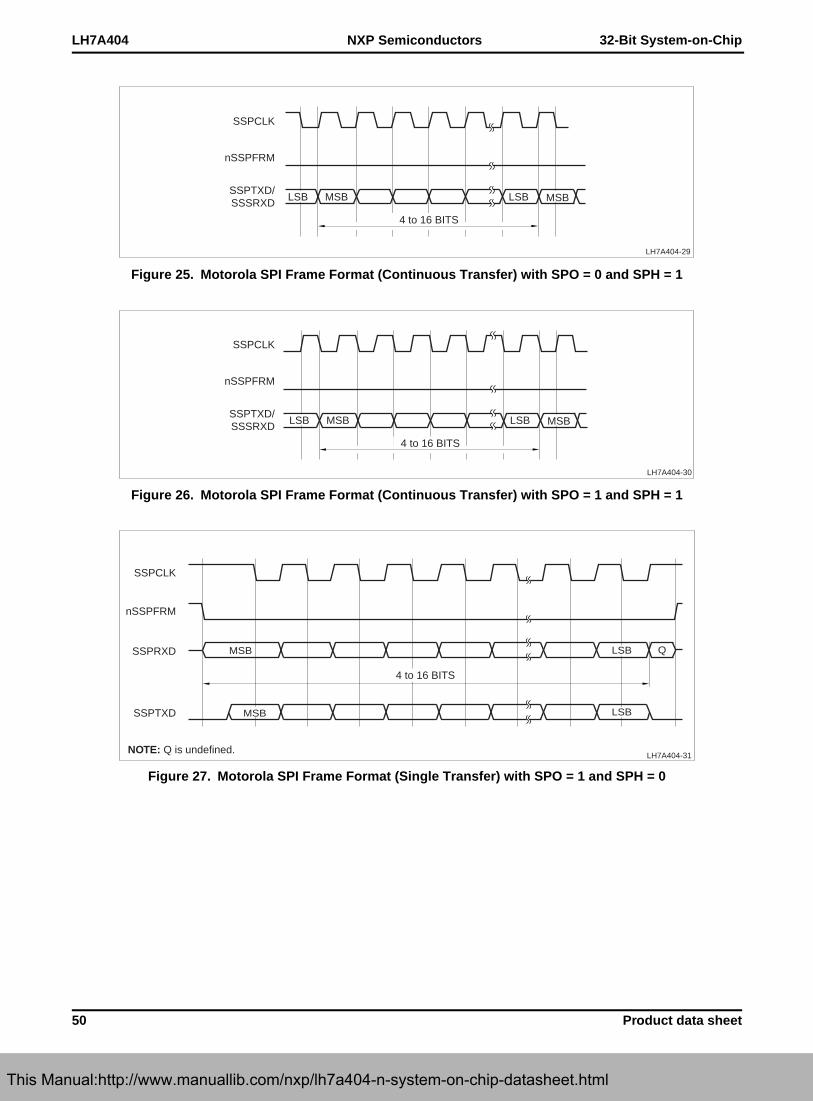
LH7A404 32-Bit System-on-Chip
50 Product data sheet
NXP Semiconductors
Figure 25. Motorola SPI Frame Format (Continuous Transfer) with SPO = 0 and SPH = 1
Figure 26. Motorola SPI Frame Format (Continuous Transfer) with SPO = 1 and SPH = 1
Figure 27. Motorola SPI Frame Format (Single Transfer) with SPO = 1 and SPH = 0
LH7A404-29
SSPCLK
nSSPFRM
SSPTXD/SSSRXD
4 to 16 BITS
LSBMSBLSB MSB
LH7A404-30
SSPCLK
nSSPFRM
SSPTXD/SSSRXD
4 to 16 BITS
LSBMSBLSB MSB
LH7A404-31
SSPCLK
nSSPFRM
SSPRXD
SSPTXD
NOTE: Q is undefined.
MSB
MSB
LSB
LSB
Q
4 to 16 BITS
This Manual:http://www.manuallib.com/nxp/lh7a404-n-system-on-chip-datasheet.html

32-Bit System-on-Chip LH7A404
Product data sheet 51
NXP Semiconductors
Figure 28. Motorola SPI Frame Format (Continuous Transfer) with SPO = 1 and SPH = 0
Figure 29. Motorola SPI Frame Format (Single Transfer) with SPO = 1 and SPH = 1
LH7A404-32
SSPCLK
nSSPFRM
SSPTXD/SSPRXD
MSBLSBMSBLSB
4 to 16 BITS
LH7A404-33
SSPCLK
nSSPFRM
SSPRXD
SSPTXD
4 to 16 BITS
MSB
MSB
Q LSB
LSB
Q
NOTE: Q is undefined.
This Manual:http://www.manuallib.com/nxp/lh7a404-n-system-on-chip-datasheet.html

LH7A404 32-Bit System-on-Chip
52 Product data sheet
NXP Semiconductors
For National Semiconductor MICROWIRE format,the serial frame pin (SSPFRM) is active LOW. Both theSSP and external slave device drive their output dataon the falling edge of the clock, and latch data from theother device on the rising edge of the clock. Unlike thefull-duplex transmission of the other two frame formats,the National Semiconductor MICROWIRE format uti-lizes a master-slave messaging technique that oper-ates in half-duplex. When a frame begins in this mode,
an 8-bit control message is transmitted to the off-chipslave. During this transmission no incoming data isreceived by the SSP. After the message has been sent,the external slave device decodes the message. Afterwaiting one serial clock period after the last bit of the 8-bit control message was received it responds by return-ing the requested data. The returned data can be 4 to16 bits in length, making the total frame length between13 to 25 bits. See Figure 30 and Figure 31.
Figure 30. MICROWIRE Frame Format (Single Transfer)
Figure 31. MICROWIRE Frame Format (Continuous Transfers)
LH7A404-34
LSBMSB0
LSBMSB
8-BIT CONTROL
SSPCLK
nSSPFRM
SSPTXD
SSPRXD
4 to 16 BITSOUTPUT DATA
LH7A404-35
SSPCLK
nSSPFRM
SSPTXD
SSPRXD
4 to 16 BITSOUTPUT DATA
8-BIT CONTROL
MSB
MSB
LSB
LSB
0
LSB
MSB
This Manual:http://www.manuallib.com/nxp/lh7a404-n-system-on-chip-datasheet.html

32-Bit System-on-Chip LH7A404
Product data sheet 53
NXP Semiconductors
Figure 32. General SSP Timing
SSPCLK(ProgrammableCLOCK phase)
SSPFRM(ProgrammableFRAME phase
and duration)
SSPRX
SSPTX
CLOCKPHASE 1
CLOCKPHASE 2
BITnOUTPUT
BITnINPUT
BITn-1OUTPUT
BITn-1INPUT
tOVTX
tISRX
tOVFRM tOHFRM
tIHRX
tOHTX
tCLK
LH7A404-199
This Manual:http://www.manuallib.com/nxp/lh7a404-n-system-on-chip-datasheet.html

LH7A404 32-Bit System-on-Chip
54 Product data sheet
NXP Semiconductors
PC Card (PCMCIA) WaveformsFigure 33 shows the waveforms for PCMCIA Read
transactions and Figure 34 shows the waveforms andtiming for Write transactions. Figure 35 shows the pre-charge, access, and hold timing relationships.
Figure 33. PCMCIA Read Transfer
tOVDREG
HCLK
A[25:0]
tOVPCD
tISD
tOVOE
tOHDREG
ADDRESS
PRECHARGE TIME
(See Note 1)
ACCESS TIME
(See Note 1)
HOLD TIME
(See Note 1)
tOHPCD
DATA
tIHD
tOHOE
tOVCEx
tOHCEx
LH7A404-15
nPCREG
nPCCEx(See Note 2)
PCDIR
D[31:0]
nPCOE/nPCIOR
NOTES: 1. Precharge time, access time, and hold time are programmable wait-state times.
2. nPCCE1
0 0 1 1
nPCCE2
0 1 0 1
TRANSFER TYPE
Common Memory Attribute Memory
I/O None
This Manual:http://www.manuallib.com/nxp/lh7a404-n-system-on-chip-datasheet.html

32-Bit System-on-Chip LH7A404
Product data sheet 55
NXP Semiconductors
Figure 34. PCMCIA Write Transfer
Figure 35. PCMCIA Precharge, Access, and Hold Waveform
tOVDREG
HCLK
A[25:0]
tOVPCD
tOVD
tOVWE
tOHDREG
ADDRESS
PRECHARGE TIME
(See Note 1)
ACCESS TIME
(See Note 1)
HOLD TIME
(See Note 1)
tOHD
tOHWE
tOVCEx
tOHCEx
LH7A404-16
nPCREG
nPCCEx (See Note 2)
PCDIR
D[15:0]
nPCWE/nPCIOW
NOTES: 1. Precharge time, access time, and hold time are programmable wait-state times.
2. nPCCE1
0 0 1 1
nPCCE2
0 1 0 1
TRANSFER TYPE
Common Memory Attribute Memory
I/O None
DATA
LH7A404-194
ACCESS
PRECHARGE
nPCWE,nPCOE,nPCIOW,nPCIOR
nCSx
HOLD
This Manual:http://www.manuallib.com/nxp/lh7a404-n-system-on-chip-datasheet.html
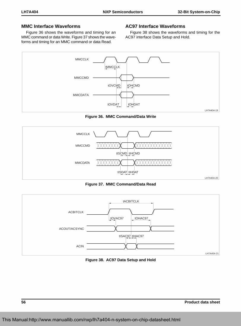
LH7A404 32-Bit System-on-Chip
56 Product data sheet
NXP Semiconductors
MMC Interface WaveformsFigure 36 shows the waveforms and timing for an
MMC command or data Write. Figure 37 shows the wave-forms and timing for an MMC command or data Read.
AC97 Interface WaveformsFigure 38 shows the waveforms and timing for the
AC97 interface Data Setup and Hold.
Figure 36. MMC Command/Data Write
Figure 37. MMC Command/Data Read
Figure 38. AC97 Data Setup and Hold
tOVCMD
MMCCLK
MMCCMD
MMCDATA
tOHCMD
tMMCCLK
tOVDAT tOHDAT
LH7A404-19
tISCMD
MMCCLK
MMCCMD
MMCDATA
tIHCMD
tISDAT tIHDAT
LH7A404-20
tOVAC97
ACBITCLK
ACOUT/ACSYNC
ACIN
tISAC97 tIHAC97
tOHAC97
tACBITCLK
LH7A404-21
This Manual:http://www.manuallib.com/nxp/lh7a404-n-system-on-chip-datasheet.html
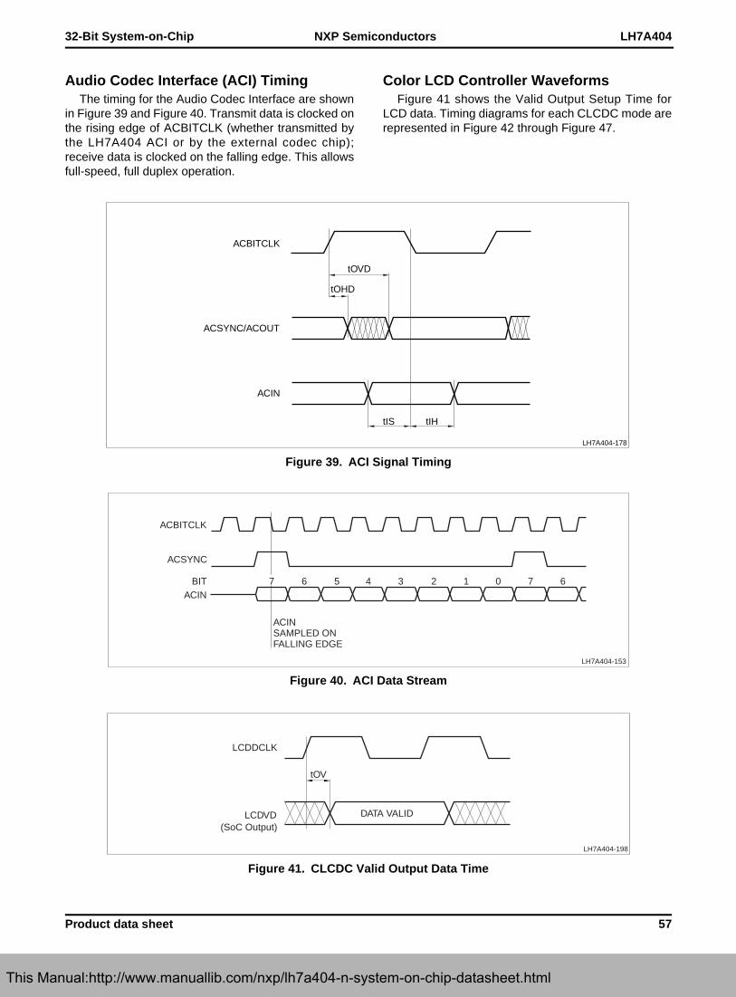
32-Bit System-on-Chip LH7A404
Product data sheet 57
NXP Semiconductors
Audio Codec Interface (ACI) TimingThe timing for the Audio Codec Interface are shown
in Figure 39 and Figure 40. Transmit data is clocked onthe rising edge of ACBITCLK (whether transmitted bythe LH7A404 ACI or by the external codec chip);receive data is clocked on the falling edge. This allowsfull-speed, full duplex operation.
Color LCD Controller WaveformsFigure 41 shows the Valid Output Setup Time for
LCD data. Timing diagrams for each CLCDC mode arerepresented in Figure 42 through Figure 47.
Figure 39. ACI Signal Timing
Figure 40. ACI Data Stream
Figure 41. CLCDC Valid Output Data Time
tOVD
tOHD
tIS tIH
ACBITCLK
ACSYNC/ACOUT
ACIN
LH7A404-178
LH7A404-153
ACBITCLK
ACSYNC
ACIN
ACINSAMPLED ONFALLING EDGE
7 6BIT 5 4 3 2 1 0 7 6
LCDDCLK
DATA VALID
tOV
LH7A404-198
LCDVD(SoC Output)
This Manual:http://www.manuallib.com/nxp/lh7a404-n-system-on-chip-datasheet.html
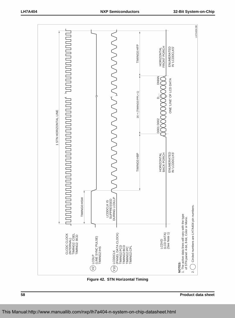
LH7A404 32-Bit System-on-Chip
58 Product data sheet
NXP Semiconductors
Figure 42. STN Horizontal Timing
1 S
TN
HO
RIZ
ON
TA
L LI
NE
CLC
DC
CLO
CK
(IN
TE
RN
AL)
TIM
ING
2: C
SE
LT
IMIN
G2:
BC
D
LCD
LP(L
INE
SY
NC
PU
LSE
)T
IMIN
G2:
IHS
LCD
DC
LK(P
AN
EL
DA
TA
CLO
CK
)T
IMIN
G2:
PC
DT
IMIN
G2:
BC
DT
IMIN
G2:
IPC
TIM
ING
2:C
PL
LCD
VD
(LC
D D
AT
A)
(See
Not
e 1)
NO
TE
S:
1. T
he a
ctiv
e da
ta li
nes
will
var
y w
ith th
e ty
pe
of S
TN
pan
el: 4
-bit,
8-b
it, C
olor
or
Mon
o.
2.
Circ
led
num
bers
are
LH
7A40
4 pi
n nu
mbe
rs.
TIM
ING
0:H
SW
TIM
ING
0:H
BP
D00
1 D
002
D...
.
ON
E 'L
INE
' OF
LC
D D
AT
A
DN
NN
TIM
ING
0:H
FP
HO
RIZ
ON
TA
LB
AC
K P
OR
CH
HO
RIZ
ON
TA
LF
RO
NT
PO
RC
H
EN
UM
ER
AT
ED
IN 'L
CD
DC
LKS
'E
NU
ME
RA
TE
DIN
'LC
DD
CLK
S'
LH7A
404-
98
LCD
DC
LK IS
SU
PP
RE
SS
ED
DU
RIN
G L
CD
LLP
V2
Y10
16 ×
(T
IMIN
G0:
PP
L+1)
This Manual:http://www.manuallib.com/nxp/lh7a404-n-system-on-chip-datasheet.html
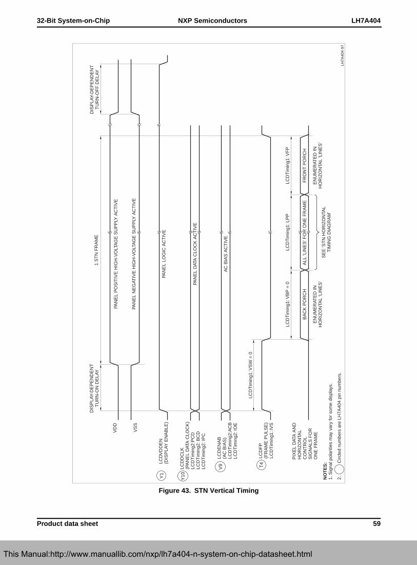
32-Bit System-on-Chip LH7A404
Product data sheet 59
NXP Semiconductors
Figure 43. STN Vertical Timing
VD
D
DIS
PLA
Y-D
EP
EN
DE
NT
TU
RN
-ON
DE
LAY
1 S
TN
FR
AM
E
PAN
EL
PO
SIT
IVE
HIG
H-V
OLT
AG
E S
UP
PLY
AC
TIV
E
PAN
EL
NE
GAT
IVE
HIG
H-V
OLT
AG
E S
UP
PLY
AC
TIV
E
PAN
EL
LOG
IC A
CT
IVE
PAN
EL
DAT
A C
LOC
K A
CT
IVE
AC
BIA
S A
CT
IVE
BA
CK
PO
RC
H
EN
UM
ER
ATE
D IN
HO
RIZ
ON
TAL
'LIN
ES
'S
EE
'ST
N H
OR
IZO
NTA
LT
IMIN
G D
IAG
RA
M'
EN
UM
ER
ATE
D IN
HO
RIZ
ON
TAL
'LIN
ES
'
FR
ON
T P
OR
CH
ALL
'LIN
ES
' FO
R O
NE
FR
AM
E
VS
S
LCD
VD
DE
N(D
ISP
LAY
EN
AB
LE)
LCD
DC
LK(P
AN
EL
DAT
A C
LOC
K)
LCD
Tim
ing2
:PC
DLC
DT
imin
g2: B
CD
LCD
Tim
ing2
: IP
C
LCD
EN
AB
(AC
BIA
S)
LCD
Tim
ing2
:AC
BLC
DT
imin
g2: I
OE
LCD
FP
(FR
AM
E P
ULS
E)
LCD
Tim
ing1
: IV
S
PIX
EL
DAT
A A
ND
HO
RIZ
ON
TAL
CO
NT
RO
LS
IGN
ALS
FO
RO
NE
FR
AM
E
NO
TE
S:
1. S
igna
l pol
ariti
es m
ay v
ary
for
som
e di
spla
ys.
2.
Circ
led
num
bers
are
LH
7A40
4 pi
n nu
mbe
rs.
LCD
Tim
ing1
: VB
P =
0LC
DT
imin
g1: L
PP
LCD
Tim
ing1
: VF
P
LCD
Tim
ing1
: VS
W =
0
Y10Y1
V9 T4
LH7A
404-
97
DIS
PLA
Y-D
EP
EN
DE
NT
TU
RN
-OF
F D
ELA
Y
This Manual:http://www.manuallib.com/nxp/lh7a404-n-system-on-chip-datasheet.html
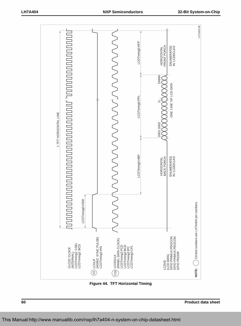
LH7A404 32-Bit System-on-Chip
60 Product data sheet
NXP Semiconductors
Figure 44. TFT Horizontal Timing
1 T
FT
HO
RIZ
ON
TAL
LIN
E
CLC
DC
CLO
CK
(IN
TE
RN
AL)
LCD
Tim
ing2
: CS
EL
LCD
Tim
ing2
: BC
D
LCD
LP(H
OR
IZ. S
YN
C P
ULS
E)
LCD
Tim
ing2
:IHS
LCD
DC
LK(P
AN
EL
DAT
A C
LOC
K)
LCD
Tim
ing2
:PC
DLC
DT
imin
g2:B
CD
LCD
Tim
ing2
:IPC
LCD
Tim
ing2
:CP
L
LCD
VD
(LC
D D
ATA
)G
PIO
PIN
MU
X:P
DO
CO
NG
PIO
PIN
MU
X:P
EO
CO
NG
PIO
PE
DD
R
NO
TE
:
Circ
led
num
bers
are
LH
7A40
4 pi
n nu
mbe
rs.
LCD
Tim
ing0
:HS
W
LCD
Tim
ing0
:HB
PLC
DT
imin
g0:P
PL
D00
1 D
002
D...
.
ON
E 'L
INE
' OF
LC
D D
ATAD
NN
N
LCD
Tim
ing0
:HF
P
HO
RIZ
ON
TAL
BA
CK
PO
RC
HH
OR
IZO
NTA
LF
RO
NT
PO
RC
H
EN
UM
ER
ATE
DIN
'LC
DD
CLK
S'
EN
UM
ER
ATE
DIN
'LC
DD
CLK
S'
LH7A
404-
96
V2
Y10
This Manual:http://www.manuallib.com/nxp/lh7a404-n-system-on-chip-datasheet.html

32-Bit System-on-Chip LH7A404
Product data sheet 61
NXP Semiconductors
Figure 45. TFT Vertical Timing
VD
D
See
Not
e 2
DIS
PLA
Y-D
EP
EN
DE
NT
TU
RN
-ON
DE
LAY
1 T
FT
FR
AM
E
PAN
EL
PO
SIT
IVE
HIG
H-V
OLT
AG
E S
UP
PLY
AC
TIV
E
PAN
EL
NE
GAT
IVE
HIG
H-V
OLT
AG
E S
UP
PLY
AC
TIV
E
PAN
EL
LOG
IC A
CT
IVE
PAN
EL
DAT
A C
LOC
K A
CT
IVE
DAT
A E
NA
BLE
BA
CK
PO
RC
H
EN
UM
ER
ATE
D IN
HO
RIZ
ON
TAL
'LIN
ES
'S
EE
'TF
T H
OR
IZO
NTA
LT
IMIN
G D
IAG
RA
M'
EN
UM
ER
ATE
D IN
HO
RIZ
ON
TAL
'LIN
ES
'
FR
ON
T P
OR
CH
ALL
'LIN
ES
' FO
R O
NE
FR
AM
E
VS
S
LCD
VD
DE
N(D
ISP
LAY
EN
AB
LEF
OR
HIG
H-V
OLT
AG
ES
UP
PLI
ES
)
LCD
DC
LK(P
AN
EL
DAT
A C
LOC
K)
LCD
Tim
ing2
:PC
DLC
DT
imin
g2: B
CD
LCD
Tim
ing2
: IP
C
LCD
EN
AB
(DAT
A E
NA
BLE
)LC
DT
imin
g2:A
CB
LCD
Tim
ing2
: IO
E
LCD
FP
(VE
RT
ICA
L S
YN
C P
ULS
E)
LCD
Tim
ing1
: IV
S
PIX
EL
DAT
A A
ND
HO
RIZ
ON
TAL
CO
NT
RO
LS
IGN
ALS
FO
RO
NE
FR
AM
E
NO
TE
S:
1. S
igna
l pol
artie
s m
ay v
ary
for
som
e di
spla
ys.
2. T
he u
se o
f HR
-CLP
for
high
-vol
tage
pow
er c
ontr
ol is
opt
iona
l on
som
e T
FT
pan
els.
3.
Circ
led
num
bers
are
LH
7A40
4 pi
n nu
mbe
rs.
DIS
PLA
YD
EP
EN
DE
NT
TU
RN
-OF
F D
ELA
Y
LCD
Tim
ing1
: VB
PLC
DT
imin
g1: L
PP
LCD
Tim
ing1
: VF
P
LCD
Tim
ing1
: VS
W
Y10
Y1
V9 T4
LH7A
404-
95
This Manual:http://www.manuallib.com/nxp/lh7a404-n-system-on-chip-datasheet.html

LH7A404 32-Bit System-on-Chip
62 Product data sheet
NXP Semiconductors
Figure 46. AD-TFT and HR-TFT Horizontal Timing
Figure 47. AD-TFT and HR-TFT Timing
1 AD-TFT or HR-TFT HORIZONTAL LINE
TIMING0:HSW
TIMING0:HSW +TIMING0:HBP
PIXEL DATA
1 LCDDCLK
002 003 004 005 006 318317 319 320001
1 LCDDCLK
ALITIMING1:LPDEL
ALITIMING1:PSCLS
ALITIMING1:REVDEL
ALITIMING2:PS2CLS2
ALITIMING2:SPLDEL
002 003 004 005 006 007 008 320001
CLCDC CLOCK(INTERNAL)PERIPHCLKSEL2:LCSRCPERIPHCLKCTRL2:LCDCLKLCDCLKPRESCALE:LCDPSVAL(SHOWN FOR REFERENCE)
LCDLP(HORIZONTAL SYNC PULSE)
INP
UT
S T
O T
HE
ALI
FR
OM
TH
E C
LCD
CO
UT
PU
TS
FR
OM
TH
EA
LI T
O T
HE
PA
NE
L
LCDDCLK(PANEL DATA CLOCK)TIMING2:PCDTIMING2:BCDTIMING2:IPCTIMING2:CPL
LCDVD[17:0]16 × (TIMING0:PPL+1)
LCDDCLK(DELAYED FOR HR-TFT)
LCDVD[17:0](DELAYED FOR HR-TFT)
LCDSPL(LINE START PULSE LEFT)
LCDLP(HORIZONTAL SYNC PULSE)
LCDCLS
LCDPS
LCDREV
LCDENAB(INTERNAL DATA ENABLE)
Y10
V3
U3
V5
W3
V2
NOTE: Circled numbers are LH7A404 pin numbers.LH7A404-188
LCDSPS(Vertical Sync)
LCDHRLP(Horizontal Sync)
LCDVD(LCD Data)
LCDSPL
LH7A404-78
LCDTiming1:VSW
1.5 µs - 4 µs
2x H-LINE
T4
V2
V3
This Manual:http://www.manuallib.com/nxp/lh7a404-n-system-on-chip-datasheet.html
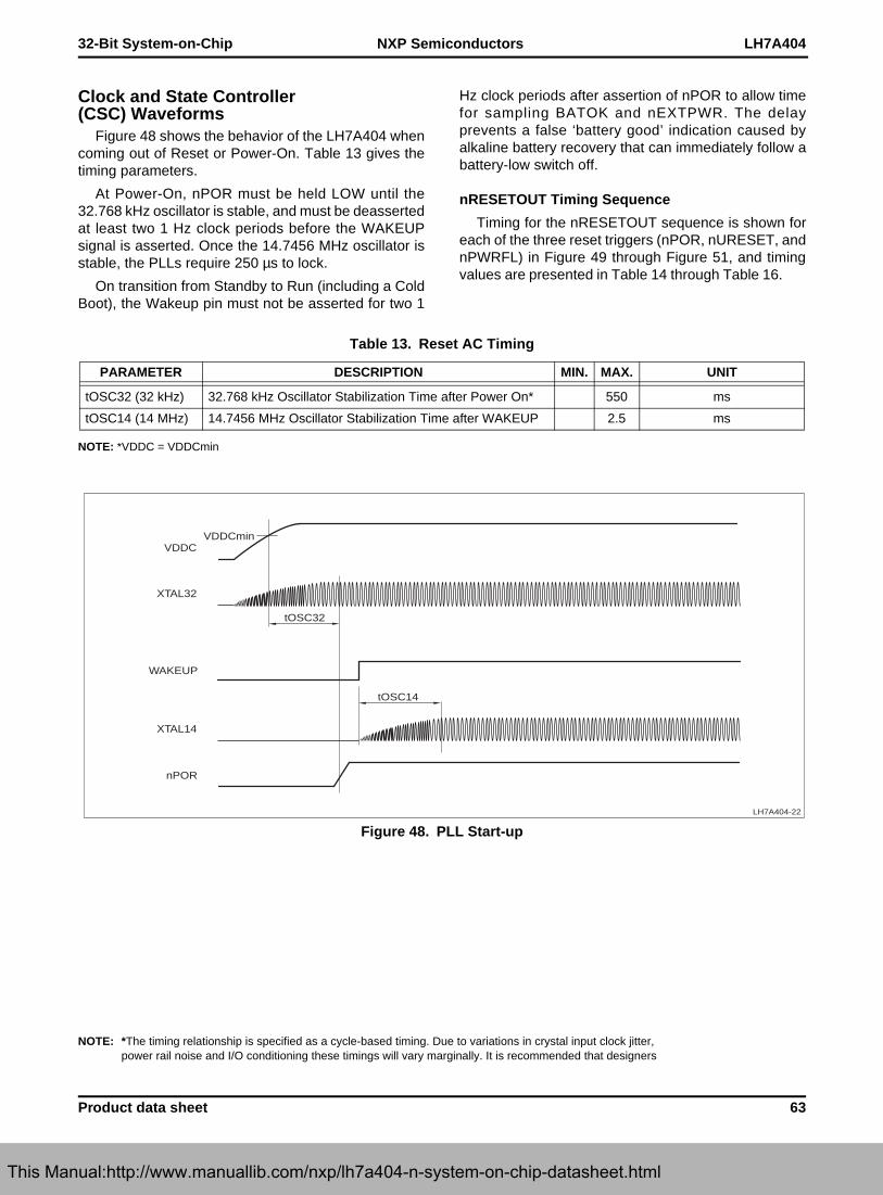
32-Bit System-on-Chip LH7A404
Product data sheet 63
NXP Semiconductors
Clock and State Controller (CSC) Waveforms
Figure 48 shows the behavior of the LH7A404 whencoming out of Reset or Power-On. Table 13 gives thetiming parameters.
At Power-On, nPOR must be held LOW until the32.768 kHz oscillator is stable, and must be deassertedat least two 1 Hz clock periods before the WAKEUPsignal is asserted. Once the 14.7456 MHz oscillator isstable, the PLLs require 250 µs to lock.
On transition from Standby to Run (including a ColdBoot), the Wakeup pin must not be asserted for two 1
Hz clock periods after assertion of nPOR to allow timefor sampling BATOK and nEXTPWR. The delayprevents a false ‘battery good’ indication caused byalkaline battery recovery that can immediately follow abattery-low switch off.
nRESETOUT Timing Sequence
Timing for the nRESETOUT sequence is shown foreach of the three reset triggers (nPOR, nURESET, andnPWRFL) in Figure 49 through Figure 51, and timingvalues are presented in Table 14 through Table 16.
NOTE: *VDDC = VDDCmin
NOTE: *The timing relationship is specified as a cycle-based timing. Due to variations in crystal input clock jitter, power rail noise and I/O conditioning these timings will vary marginally. It is recommended that designers
Table 13. Reset AC Timing
PARAMETER DESCRIPTION MIN. MAX. UNIT
tOSC32 (32 kHz) 32.768 kHz Oscillator Stabilization Time after Power On* 550 ms
tOSC14 (14 MHz) 14.7456 MHz Oscillator Stabilization Time after WAKEUP 2.5 ms
Figure 48. PLL Start-up
LH7A404-22
tOSC32
VDDC VDDCmin
XTAL32
nPOR
tOSC14
XTAL14
WAKEUP
This Manual:http://www.manuallib.com/nxp/lh7a404-n-system-on-chip-datasheet.html

LH7A404 32-Bit System-on-Chip
64 Product data sheet
NXP Semiconductors
add some timing margin to avoid any possible corner case condition.
NOTE: *The timing relationship is specified as a cycle-based timing. Due to variations in crystal input clock jitter, power rail noise and I/O conditioning these timings will vary marginally. It is recommended that designers
Figure 49. nRESETOUT Timing for nPOR Trigger
Table 14. nRESETOUT Timing Values for nPOR Trigger
SIGNAL MIN. TYP. MAX. UNITS DESCRIPTION
tDA_nPOR_nRSTO 30 ns nPOR to nRESETOUT assertion delay
tDD_nPOR_nRSTO 30 ns nPOR to nRESETOUT deassertion delay
tDD_nPOR_WKUP 2 1 Hz Periods* nPOR deassertion to WAKEUP assert delay
tA_WKUP 4 XTAL32 Periods* WAKEUP assertion time
tDA_nPOR_CLKEN 30 ns nURESET assertion to CLKEN deassertion delay
tDA_WKUP_CLKEN 2 4 XTAL32 Periods* WAKEUP to CLKEN assertion delay
nPOR
WAKEUP
nRESETOUT
CLKEN
tDD_nPOR_WKUP tA_WKUP
tDA_nPOR_CLKENtDA_nPOR_nRSTO tDA_WKUP_CLKEN
LH7A404-202
tDD_nPOR_nRSTO
TRIGGERPOINT
This Manual:http://www.manuallib.com/nxp/lh7a404-n-system-on-chip-datasheet.html

32-Bit System-on-Chip LH7A404
Product data sheet 65
NXP Semiconductors
add some timing margin to avoid any possible corner case condition.
NOTE: *The timing relationship is specified as a cycle-based timing. Due to variations in crystal input clock jitter, power rail noise and I/O conditioning these timings will vary marginally. It is recommended that designers
Figure 50. nRESETOUT Timing for nURESET Trigger
Table 15. nRESETOUT Timing Values for nURESET Trigger
SIGNAL MIN. TYP. MAX. UNITS DESCRIPTION
tDA_nURESET_nRSTO 2 4 XTAL32 Periods* nURESET to nRESETOUT assertion delay
tDD_nURESET_nRSTO 0 2 XTAL32 Periods* nURESET to nRESETOUT deassertion delay
tA_nURESET 4 XTAL32 Periods* nURESET assertion time
tDD_nURESET_WKUP 2 XTAL32 Periods* nURESET deassertion to WAKEUP assertion delay
tA_WKUP 4 XTAL32 Periods* WAKEUP assertion time
tDA_nURESET_CLKEN 2 4 XTAL32 Periods* nURESET assertion to CLKEN deassertion delay
tDA_WKUP_CLKEN 2 4 XTAL32 Periods* WAKEUP to CLKEN assertion delay
nURESET
WAKEUP
nRESETOUT
CLKEN
tDD_nURESET_WKUP tA_WKUPtA_nURESET
tDA_nURESET_CLKENtDA_nURESET_nRSTO tDA_WKUP_CLKEN
LH7A404-201
tDD_nURESET_nRSTO
TRIGGERPOINT
This Manual:http://www.manuallib.com/nxp/lh7a404-n-system-on-chip-datasheet.html
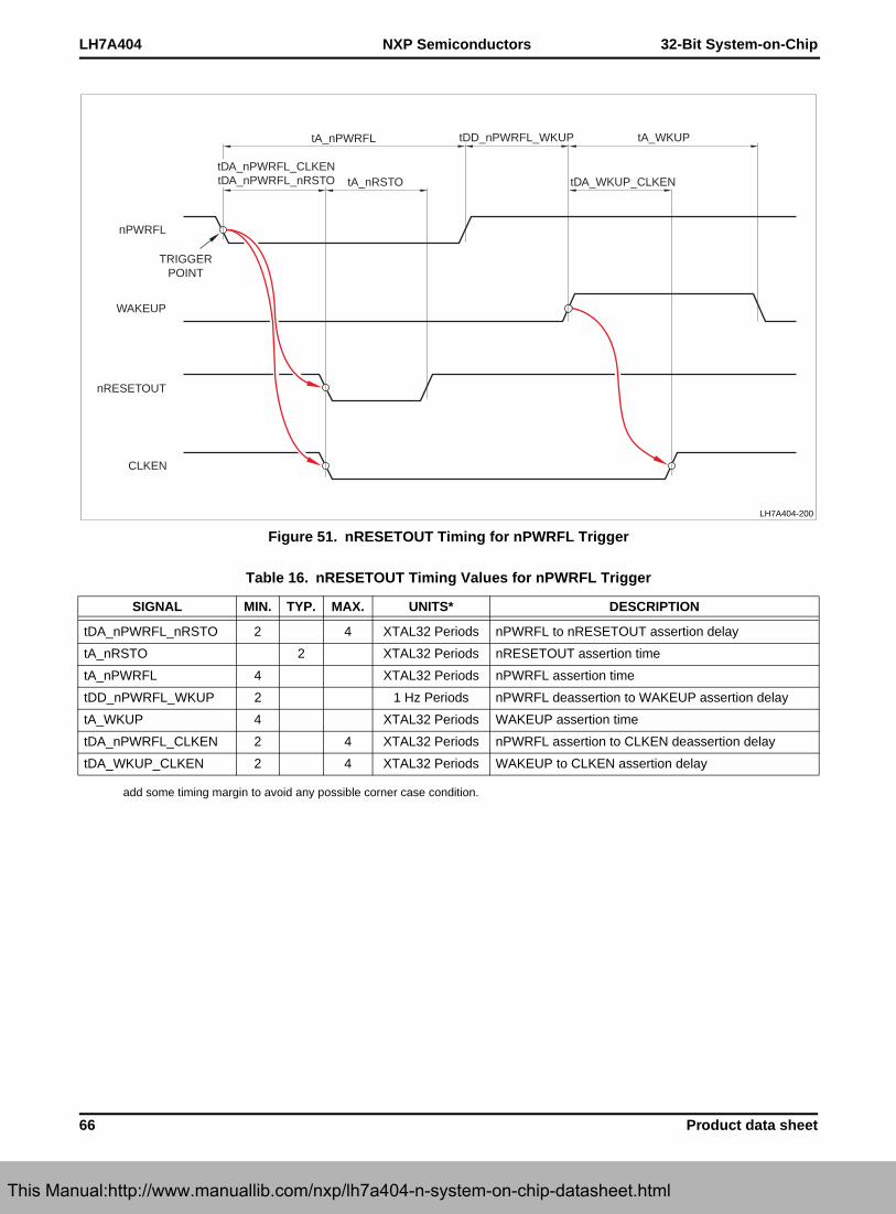
LH7A404 32-Bit System-on-Chip
66 Product data sheet
NXP Semiconductors
add some timing margin to avoid any possible corner case condition.
Figure 51. nRESETOUT Timing for nPWRFL Trigger
Table 16. nRESETOUT Timing Values for nPWRFL Trigger
SIGNAL MIN. TYP. MAX. UNITS* DESCRIPTION
tDA_nPWRFL_nRSTO 2 4 XTAL32 Periods nPWRFL to nRESETOUT assertion delay
tA_nRSTO 2 XTAL32 Periods nRESETOUT assertion time
tA_nPWRFL 4 XTAL32 Periods nPWRFL assertion time
tDD_nPWRFL_WKUP 2 1 Hz Periods nPWRFL deassertion to WAKEUP assertion delay
tA_WKUP 4 XTAL32 Periods WAKEUP assertion time
tDA_nPWRFL_CLKEN 2 4 XTAL32 Periods nPWRFL assertion to CLKEN deassertion delay
tDA_WKUP_CLKEN 2 4 XTAL32 Periods WAKEUP to CLKEN assertion delay
tA_nPWRFL
nPWRFL
TRIGGERPOINT
WAKEUP
nRESETOUT
CLKEN
tDD_nPWRFL_WKUP tA_WKUP
tDA_WKUP_CLKENtA_nRSTO
LH7A404-200
tDA_nPWRFL_CLKENtDA_nPWRFL_nRSTO
This Manual:http://www.manuallib.com/nxp/lh7a404-n-system-on-chip-datasheet.html
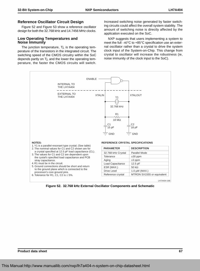
32-Bit System-on-Chip LH7A404
Product data sheet 67
NXP Semiconductors
Reference Oscillator Circuit DesignFigure 52 and Figure 53 show a reference oscillator
design for both the 32.768 kHz and 14.7456 MHz clocks.
Low Operating Temperatures and Noise Immunity
The junction temperature, Tj, is the operating tem-perature of the transistors in the integrated circuit. Theswitching speed of the CMOS circuitry within the SoCdepends partly on Tj, and the lower the operating tem-perature, the faster the CMOS circuits will switch.
Increased switching noise generated by faster switch-ing circuits could affect the overall system stability. Theamount of switching noise is directly affected by theapplication executed on the SoC.
NXP suggests that users implementing a system tomeet the full 40°C to +85°C specification use an exter-nal oscillator rather than a crystal to drive the systemclock input of the System-on-Chip. This change fromcrystal to oscillator will increase the robustness (ie,noise immunity of the clock input to the SoC).
Figure 52. 32.768 kHz External Oscillator Components and Schematic
ENABLE
XTALIN XTALOUT
GND
NOTES:1. Y1 is a parallel-resonant type crystal. (See table)2. The nominal values for C1 and C2 shown are for a crystal specified at 12.5 pF load capacitance (CL).3. The values for C1 and C2 are dependent upon the cystal's specified load capacitance and PCB stray capacitance.4. R1 must be in the circuit.5. Ground connections should be short and return to the ground plane which is connected to the processor's core ground pins.6. Tolerance for R1, C1, C2 is ≤ 5%.
GND
32.768 kHz
18 MΩ
LH7A404-168
PARAMETER DESCRIPTION
32.768 kHz CrystalToleranceAgingLoad CapacitanceESR (MAX.)Drive LevelReference crystal
Parallel Mode±30 ppm±3 ppm12.5 pF50 kΩ1.0 µW (MAX.)MTRON SX1555 or equivalent
C115 pF
C218 pF
R1
Y1
INTERNAL TOTHE LH7A404
EXTERNAL TOTHE LH7A404
REFERENCE CRYSTAL SPECIFICATIONS
This Manual:http://www.manuallib.com/nxp/lh7a404-n-system-on-chip-datasheet.html
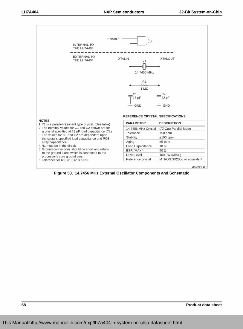
LH7A404 32-Bit System-on-Chip
68 Product data sheet
NXP Semiconductors
Figure 53. 14.7456 MHz External Oscillator Components and Schematic
ENABLE
XTALIN XTALOUT
GND
NOTES:1. Y1 is a parallel-resonant type crystal. (See table)2. The nominal values for C1 and C2 shown are for a crystal specified at 18 pF load capacitance (CL).3. The values for C1 and C2 are dependent upon the cystal's specified load capacitance and PCB stray capacitance.4. R1 must be in the circuit.5. Ground connections should be short and return to the ground plane which is connected to the processor's core ground pins.6. Tolerance for R1, C1, C2 is ≤ 5%.
GND
14.7456 MHz
1 MΩ
LH7A404-167
C118 pF
C222 pF
R1
Y1
INTERNAL TOTHE LH7A404
EXTERNAL TOTHE LH7A404
PARAMETER DESCRIPTION
14.7456 MHz CrystalToleranceStabilityAgingLoad CapacitanceESR (MAX.)Drive LevelReference crystal
(AT-Cut) Parallel Mode±50 ppm±100 ppm±5 ppm18 pF40 Ω100 µW (MAX.)MTRON SX2050 or equivalent
REFERENCE CRYSTAL SPECIFICATIONS
This Manual:http://www.manuallib.com/nxp/lh7a404-n-system-on-chip-datasheet.html

32-Bit System-on-Chip LH7A404
Product data sheet 69
NXP Semiconductors
Printed Circuit Board Layout PracticesLH7A404 POWER SUPPLY DECOUPLING
The LH7A404 has separate power and ground pinsfor different internal circuitry sections. The VDD andVSS pins supply power to I/O buffers, while VDDC andVSSC supply power to the core logic, and VDDA/VSSAsupply analog power to the PLLs.
Each of the VDD and VDDC pins must be providedwith a low impedance path to the corresponding boardpower supply. Likewise, the VSS and VSSC pins must beprovided with a low impedance path to the board ground.
Each power supply must be decoupled to groundusing at least one 0.1 F high frequency capacitorlocated as close as possible to a VDDx-VSSx pin pairon each of the four sides of the chip. If room on the cir-cuit board allows, add one 0.01 F high frequencycapacitor near each VDDx-VSSx pair on the chip.
To be effective, the capacitor leads and associatedcircuit board traces connecting to the chip VDDx-VSSxpins must be kept to less than half an inch (12.7 mm)per capacitor lead. There must be one bulk 10 Fcapacitor for each power supply placed near one sideof the chip.
REFERENCE PLL, VDDA, VSSA FILTERThe VDDA pins supply power to the chip PLL cir-
cuitry. VSSA is the ground return path for the PLL cir-cuit. NXP recommends a low-pass filter attached asshown in Figure 54. The values of the inductor andcapacitors are not critical. The low-pass filter preventshigh frequency noise from adversely affecting the PLLcircuits. The distance from the IC pin to the high fre-quency capacitor should be as short as possible.
UNUSED INPUT SIGNAL CONDITIONINGFloating input signals can cause excessive power
consumption. Unused inputs without internal pull-up orpull-down resistors should be pulled up or down exter-nally, to tie the signal to its inactive state. NXP recom-mends using no larger than 33 k.
Some GPIO signals may default to inputs. If the pinsthat carry these signals are unused, software can pro-gram these signals as outputs, eliminating the need forpull-ups or pull-downs. Power consumption may behigher than expected until software completes pro-gramming the GPIO. Some LH7A404 inputs have inter-nal pull-ups or pull-downs. If unused, these inputs donot require external conditioning.
OTHER CIRCUIT BOARD LAYOUT PRACTICESAll outputs have fast rise and fall times. Printed cir-
cuit trace interconnection length must therefore bereduced to minimize overshoot, undershoot and reflec-tions caused by transmission line effects of these fastoutput switching times. This recommendation particu-larly applies to the address and data buses.
When considering capacitance, calculations mustconsider all device loads and capacitances due to thecircuit board traces. Capacitance due to the traces willdepend upon a number of factors, including the tracewidth, dielectric material the circuit board is made fromand proximity to ground and power planes.
Attention to power supply decoupling and printed cir-cuit board layout becomes more critical in systems withhigher capacitive loads. As these capacitive loadsincrease, transient currents in the power supply andground return paths also increase.
Figure 54. VDDA, VSSA Filter Circuit
LH7A404-169
VDDAx
VDDC
VSSAx
22 µF
VDDC(SOURCE)
0.1 µF+
LH7A40410 µH
This Manual:http://www.manuallib.com/nxp/lh7a404-n-system-on-chip-datasheet.html
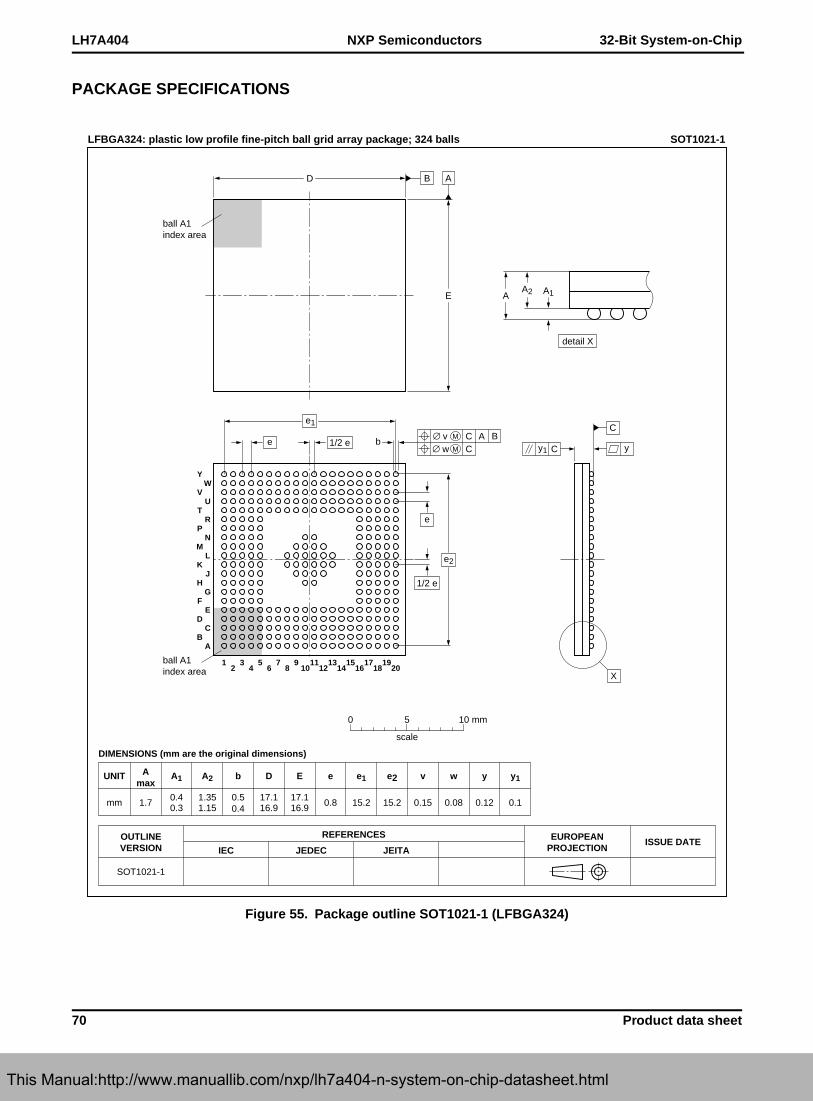
LH7A404 32-Bit System-on-Chip
70 Product data sheet
NXP Semiconductors
PACKAGE SPECIFICATIONS
Figure 55. Package outline SOT1021-1 (LFBGA324)
REFERENCESOUTLINEVERSION
EUROPEANPROJECTION
ISSUE DATEIEC JEDEC JEITA
SOT1021-1
SOT1021-1
07-07-0707-07-07
UNIT Amax
mm 1.7 0.40.3
1.351.15
17.116.9
17.116.9 0.8 15.2 0.15 0.08 0.1
A1
DIMENSIONS (mm are the original dimensions)
LFBGA324: plastic low profile fine-pitch ball grid array package; 324 balls
0 5 10 mm
scale
A2 b
0.50.4
D E e e1 e2
15.2
v w y
0.12
y1
C
yCy1
X
AB
CD
EF
H
K
G
L
J
MN
PR
TU
VW
Y
2 4 6 8 10 12 14 161 3 5 7 9 11 13 15
18 2017 19
b
e2
e1
e
e
1/2 e
1/2 eAC B∅ v M
C∅ w M
ball A1index area
detail X
AA2 A1
B A
ball A1index area
E
D
This Manual:http://www.manuallib.com/nxp/lh7a404-n-system-on-chip-datasheet.html

IMPORTANT NOTICE Dear customer, As from June 1st, 2007 NXP Semiconductors has acquired the LH7xxx ARM Microcontrollers from Sharp Microelectronics. The following changes are applicable to the attached data sheet. In data sheets where the previous Sharp or Sharp Corporation references remain, please use the new links as shown below. For www.sharpsma.com use www.nxp.com/microcontrollers for indicated sales addresses use [email protected] (email) The copyright notice at the bottom of each page (or elsewhere in the document, depending on the version) - Copyright © (year) by SHARP Corporation. is replaced with: - © NXP B.V. (year). All rights reserved. If you have any questions related to the data sheet, please contact our nearest sales office via e-mail or phone (details via [email protected]). Thank you for your cooperation and understanding, In addition to that the Annex A (attached hereto) is added to the document. NXP Semiconductors
This Manual:http://www.manuallib.com/nxp/lh7a404-n-system-on-chip-datasheet.html

32-Bit System-on-Chip LH7A404
Product data sheet 71
NXP Semiconductors
REVISION HISTORY
Table 17. Revision history
Document ID Release date Data sheet status Change notice Supersedes
LH7A404_N_2 20080307 Product data sheet - LH7A404_N_1
Modifications:
• Changed status from ‘Preliminary’ to ‘Product’
• Fig. 19; replaced with correct figure.
• Fig. 20; added timing symbols.
LH7A404_N_1 20070716 Preliminary data sheet
- LH7A404 V1-5 12-1-2006
Modifications:
• First NXP version based on the LH7A404 data sheet of 20061201
This Manual:http://www.manuallib.com/nxp/lh7a404-n-system-on-chip-datasheet.html

LH7A404 32-Bit System-on-Chip
72 Product data sheet
NXP Semiconductors
1. Legal information
1.1 Data sheet status
[1] Please consult the most recently issued document before initiating or completing a design.
[2] The term ‘short data sheet’ is explained in section “Definitions”.
[3] The product status of device(s) described in this document may have changed since this document was published and may differ in case of multiple devices. The latest product status information is available on the Internet at URL http://www.nxp.com.
1.2 Definitions
Draft — The document is a draft version only. The content is still under internal review and subject to formal approval, which may result in modifications or additions. NXP Semiconductors does not give any representations or warranties as to the accuracy or completeness of information included herein and shall have no liability for the consequences of use of such information.
Short data sheet — A short data sheet is an extract from a full data sheet with the same product type number(s) and title. A short data sheet is intended for quick reference only and should not be relied upon to contain detailed and full information. For detailed and full information see the relevant full data sheet, which is available on request via the local NXP Semiconductors sales office. In case of any inconsistency or conflict with the short data sheet, the full data sheet shall prevail.
Product specification — The information and data provided in a Product data sheet shall define the specification of the product as agreed between NXP Semiconductors and its customer, unless NXP Semiconductors and customer have explicitly agreed otherwise in writing. In no event however, shall an agreement be valid in which the NXP Semiconductors product is deemed to offer functions and qualities beyond those described in the Product data sheet.
1.3 Disclaimers
Limited warranty and liability — Information in this document is believed to be accurate and reliable. However, NXP Semiconductors does not give any representations or warranties, expressed or implied, as to the accuracy or completeness of such information and shall have no liability for the consequences of use of such information. NXP Semiconductors takes no responsibility for the content in this document if provided by an information source outside of NXP Semiconductors.
In no event shall NXP Semiconductors be liable for any indirect, incidental, punitive, special or consequential damages (including - without limitation - lost profits, lost savings, business interruption, costs related to the removal or replacement of any products or rework charges) whether or not such damages are based on tort (including negligence), warranty, breach of contract or any other legal theory.
Notwithstanding any damages that customer might incur for any reason whatsoever, NXP Semiconductors’ aggregate and cumulative liability towards customer for the products described herein shall be limited in accordance with the Terms and conditions of commercial sale of NXP Semiconductors.
Right to make changes — NXP Semiconductors reserves the right to make changes to information published in this document, including without limitation specifications and product descriptions, at any time and without notice. This document supersedes and replaces all information supplied prior to the publication hereof.
Suitability for use — NXP Semiconductors products are not designed, authorized or warranted to be suitable for use in life support, life-critical or safety-critical systems or equipment, nor in applications where failure or malfunction of an NXP Semiconductors product can reasonably be expected to result in personal injury, death or severe property or environmental
damage. NXP Semiconductors and its suppliers accept no liability for inclusion and/or use of NXP Semiconductors products in such equipment or applications and therefore such inclusion and/or use is at the customer’s own risk.
Applications — Applications that are described herein for any of these products are for illustrative purposes only. NXP Semiconductors makes no representation or warranty that such applications will be suitable for the specified use without further testing or modification.
Customers are responsible for the design and operation of their applications and products using NXP Semiconductors products, and NXP Semiconductors accepts no liability for any assistance with applications or customer product design. It is customer’s sole responsibility to determine whether the NXP Semiconductors product is suitable and fit for the customer’s applications and products planned, as well as for the planned application and use of customer’s third party customer(s). Customers should provide appropriate design and operating safeguards to minimize the risks associated with their applications and products.
NXP Semiconductors does not accept any liability related to any default, damage, costs or problem which is based on any weakness or default in the customer’s applications or products, or the application or use by customer’s third party customer(s). Customer is responsible for doing all necessary testing for the customer’s applications and products using NXP Semiconductors products in order to avoid a default of the applications and the products or of the application or use by customer’s third party customer(s). NXP does not accept any liability in this respect.
Limiting values — Stress above one or more limiting values (as defined in the Absolute Maximum Ratings System of IEC 60134) will cause permanent damage to the device. Limiting values are stress ratings only and (proper) operation of the device at these or any other conditions above those given in the Recommended operating conditions section (if present) or the Characteristics sections of this document is not warranted. Constant or repeated exposure to limiting values will permanently and irreversibly affect the quality and reliability of the device.
Terms and conditions of commercial sale — NXP Semiconductors products are sold subject to the general terms and conditions of commercial sale, as published at http://www.nxp.com/profile/terms, unless otherwise agreed in a valid written individual agreement. In case an individual agreement is concluded only the terms and conditions of the respective agreement shall apply. NXP Semiconductors hereby expressly objects to applying the customer’s general terms and conditions with regard to the purchase of NXP Semiconductors products by customer.
No offer to sell or license — Nothing in this document may be interpreted or construed as an offer to sell products that is open for acceptance or the grant, conveyance or implication of any license under any copyrights, patents or other industrial or intellectual property rights.
Export control — This document as well as the item(s) described herein may be subject to export control regulations. Export might require a prior authorization from competent authorities.
Non-automotive qualified products — Unless this data sheet expressly states that this specific NXP Semiconductors product is automotive qualified, the product is not suitable for automotive use. It is neither qualified nor tested
Document status[1][2] Product status[3] Definition
Objective [short] data sheet Development This document contains data from the objective specification for product development.
Preliminary [short] data sheet Qualification This document contains data from the preliminary specification.
Product [short] data sheet Production This document contains the product specification.
This Manual:http://www.manuallib.com/nxp/lh7a404-n-system-on-chip-datasheet.html
LH7A404 32-Bit System-on-ChipNXP Semiconductors
© NXP B.V. 2008. All rights reserved.
in accordance with automotive testing or application requirements. NXP Semiconductors accepts no liability for inclusion and/or use of non-automotive qualified products in automotive equipment or applications.
In the event that customer uses the product for design-in and use in automotive applications to automotive specifications and standards, customer (a) shall use the product without NXP Semiconductors’ warranty of the product for such automotive applications, use and specifications, and (b) whenever customer uses the product for automotive applications beyond NXP Semiconductors’ specifications such use shall be solely at customer’s own risk, and (c) customer fully indemnifies NXP Semiconductors for any liability,
damages or failed product claims resulting from customer design and use of the product for automotive applications beyond NXP Semiconductors’ standard warranty and NXP Semiconductors’ product specifications.
1.4 TrademarksNotice: All referenced brands, product names, service names and trademarks are the property of their respective owners.
2. Contact information
For more information, please visit: http://www.nxp.com
For sales office addresses, please send an email to: [email protected]
This Manual:http://www.manuallib.com/nxp/lh7a404-n-system-on-chip-datasheet.html