Embed Size (px)
Citation preview
NuDAQ®
PCI-9111DG/HR Multi-Functions
Data Acquisition Card User’s Guide
Recycled Paper

©Copyright 1997~2003 ADLINK Technology Inc;
All Rights Reserved.
Manual Rev 2.50: April 4, 2003
Part No: 50-11110-102
The information in this document is subject to change without prior notice in order to improve reliability, design and function and does not represent a commitment on the part of the manufacturer.
In no event will the manufacturer be liable for direct, indirect, special, incidental, or consequential damages arising out of the use or inability to use the product or documentation, even if advised of the possibility of such damages.
This document contains proprietary information protected by copyright. All rights are reserved. No part of this manual may be reproduced by any mechanical, electronic, or other means in any form without prior written permission of the manufacturer.
Trademarks
NuDAQ®, NuIPC® are registered trademarks of ADLINK Technology Inc. Other products names mentioned herein are used for identification purposes only and may be trademarks and/or registered trademarks of their respective companies.
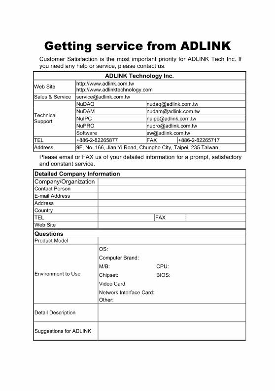
Getting service from ADLINK Customer Satisfaction is the most important priority for ADLINK Tech Inc. If you need any help or service, please contact us.
ADLINK Technology Inc.
Web Site http://www.adlink.com.tw http://www.adlinktechnology.com
Sales & Service [email protected] NuDAQ [email protected] NuDAM [email protected] NuIPC [email protected] NuPRO [email protected]
Technical Support
Software [email protected] TEL +886-2-82265877 FAX +886-2-82265717 Address 9F, No. 166, Jian Yi Road, Chungho City, Taipei, 235 Taiwan.
Please email or FAX us of your detailed information for a prompt, satisfactory and constant service.
Detailed Company Information Company/Organization Contact Person E-mail Address Address Country TEL FAX Web Site
Questions Product Model
Environment to Use
OS: Computer Brand: M/B: CPU: Chipset: BIOS: Video Card: Network Interface Card: Other:
Detail Description
Suggestions for ADLINK
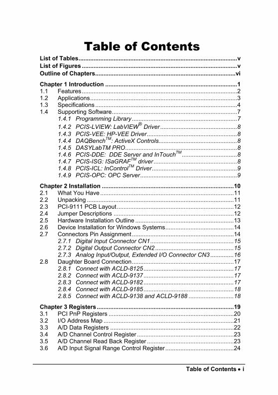
Table of Contents • i
Table of Contents List of Tables...............................................................................................v List of Figures .............................................................................................v Outline of Chapters....................................................................................vi Chapter 1 Introduction ...............................................................................1 1.1 Features.............................................................................................2 1.2 Applications........................................................................................3 1.3 Specifications .....................................................................................4 1.4 Supporting Software...........................................................................7
1.4.1 Programming Library ...............................................................7 1.4.2 PCIS-LVIEW: LabVIEW® Driver ..............................................8 1.4.3 PCIS-VEE: HP-VEE Driver......................................................8 1.4.4 DAQBenchTM: ActiveX Controls...............................................8 1.4.5 DASYLabTM PRO...................................................................8 1.4.6 PCIS-DDE: DDE Server and InTouchTM.................................8 1.4.7 PCIS-ISG: ISaGRAFTM driver ..................................................8 1.4.8 PCIS-ICL: InControlTM Driver...................................................9 1.4.9 PCIS-OPC: OPC Server..........................................................9
Chapter 2 Installation ...............................................................................10 2.1 What You Have ................................................................................11 2.2 Unpacking ........................................................................................11 2.3 PCI-9111 PCB Layout......................................................................12 2.4 Jumper Descriptions ........................................................................12 2.5 Hardware Installation Outline ...........................................................13 2.6 Device Installation for Windows Systems.........................................14 2.7 Connectors Pin Assignment .............................................................14
2.7.1 Digital Input Connector CN1..................................................15 2.7.2 Digital Output Connector CN2 ...............................................15 2.7.3 Analog Input/Output, Extended I/O Connector CN3 ..............16
2.8 Daughter Board Connection.............................................................17 2.8.1 Connect with ACLD-8125......................................................17 2.8.2 Connect with ACLD-9137......................................................17 2.8.3 Connect with ACLD-9182......................................................17 2.8.4 Connect with ACLD-9185......................................................18 2.8.5 Connect with ACLD-9138 and ACLD-9188 ...........................18
Chapter 3 Registers ..................................................................................19 3.1 PCI PnP Registers ...........................................................................20 3.2 I/O Address Map ..............................................................................21 3.3 A/D Data Registers ..........................................................................22 3.4 A/D Channel Control Register ..........................................................23 3.5 A/D Channel Read Back Register ....................................................23 3.6 A/D Input Signal Range Control Register .........................................24
ii • Table of Contents
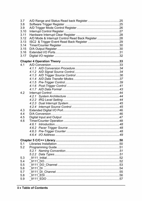
3.7 A/D Range and Status Read back Register .....................................25 3.8 Software Trigger Register ................................................................25 3.9 A/D Trigger Mode Control Register ..................................................26 3.10 Interrupt Control Register .................................................................27 3.11 Hardware Interrupt Clear Register ...................................................28 3.12 A/D Mode & Interrupt Control Read Back Register ..........................28 3.13 ISC2 & Trigger Event Read Back Register .....................................29 3.14 Timer/Counter Register ....................................................................30 3.15 D/A Output Register .........................................................................30 3.16 Extended I/O Ports...........................................................................31 3.17 Digital I/O register ............................................................................32 Chapter 4 Operation Theory ....................................................................33 4.1 A/D Conversion ................................................................................33
4.1.1 A/D Conversion Procedure....................................................34 4.1.2 A/D Signal Source Control.....................................................34 4.1.3 A/D Trigger Source Control ...................................................36 4.1.4 A/D Data Transfer Modes......................................................37 4.1.5 Pre-Trigger Control................................................................39 4.1.6 Post-Trigger Control ..............................................................41 4.1.7 A/D Data Format ...................................................................43
4.2 Interrupt Control ...............................................................................44 4.2.1 System Architecture ..............................................................44 4.2.2 IRQ Level Setting ..................................................................44 4.2.3 Dual Interrupt System............................................................45 4.2.4 Interrupt Source Control ........................................................45
4.3 Extended Digital I/O Port..................................................................46 4.4 D/A Conversion ................................................................................46 4.5 Digital Input and Output ...................................................................47 4.6 Timer/Counter Operation .................................................................48
4.6.1 Introduction............................................................................48 4.6.2 Pacer Trigger Source ............................................................48 4.6.3 Pre-Trigger Counter ..............................................................48 4.6.4 I/O Address ...........................................................................49
Chapter 5 C/C++ Library...........................................................................50 5.1 Libraries Installation .........................................................................50 5.2 Programming Guide .........................................................................51
5.2.1 Naming Convention...............................................................51 5.2.2 Data Types ............................................................................51
5.3 _9111_Initial.....................................................................................52 5.4 _9111_DO........................................................................................52 5.5 _9111_DO_Channel ........................................................................53 5.6 _9111_DI .........................................................................................54 5.7 _9111_DI_Channel ..........................................................................55 5.8 _9111_EDI .......................................................................................56 5.9 _9111_EDO .....................................................................................57
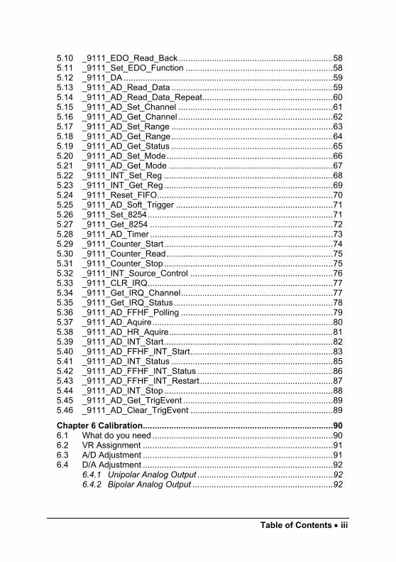
Table of Contents • iii
5.10 _9111_EDO_Read_Back.................................................................58 5.11 _9111_Set_EDO_Function ..............................................................58 5.12 _9111_DA ........................................................................................59 5.13 _9111_AD_Read_Data ....................................................................59 5.14 _9111_AD_Read_Data_Repeat.......................................................60 5.15 _9111_AD_Set_Channel .................................................................61 5.16 _9111_AD_Get_Channel .................................................................62 5.17 _9111_AD_Set_Range ....................................................................63 5.18 _9111_AD_Get_Range....................................................................64 5.19 _9111_AD_Get_Status ....................................................................65 5.20 _9111_AD_Set_Mode......................................................................66 5.21 _9111_AD_Get_Mode .....................................................................67 5.22 _9111_INT_Set_Reg .......................................................................68 5.23 _9111_INT_Get_Reg .......................................................................69 5.24 _9111_Reset_FIFO..........................................................................70 5.25 _9111_AD_Soft_Trigger ..................................................................71 5.26 _9111_Set_8254..............................................................................71 5.27 _9111_Get_8254 .............................................................................72 5.28 _9111_AD_Timer .............................................................................73 5.29 _9111_Counter_Start.......................................................................74 5.30 _9111_Counter_Read......................................................................75 5.31 _9111_Counter_Stop .......................................................................75 5.32 _9111_INT_Source_Control ............................................................76 5.33 _9111_CLR_IRQ..............................................................................77 5.34 _9111_Get_IRQ_Channel................................................................77 5.35 _9111_Get_IRQ_Status...................................................................78 5.36 _9111_AD_FFHF_Polling ................................................................79 5.37 _9111_AD_Aquire............................................................................80 5.38 _9111_AD_HR_Aquire.....................................................................81 5.39 _9111_AD_INT_Start.......................................................................82 5.40 _9111_AD_FFHF_INT_Start............................................................83 5.41 _9111_AD_INT_Status ....................................................................85 5.42 _9111_AD_FFHF_INT_Status .........................................................86 5.43 _9111_AD_FFHF_INT_Restart........................................................87 5.44 _9111_AD_INT_Stop .......................................................................88 5.45 _9111_AD_Get_TrigEvent ...............................................................89 5.46 _9111_AD_Clear_TrigEvent ............................................................89 Chapter 6 Calibration................................................................................90 6.1 What do you need ............................................................................90 6.2 VR Assignment ................................................................................91 6.3 A/D Adjustment ................................................................................91 6.4 D/A Adjustment ................................................................................92
6.4.1 Unipolar Analog Output .........................................................92 6.4.2 Bipolar Analog Output ...........................................................92
iv • Table of Contents
Chapter 7 Software Utility ........................................................................93 7.1 9111util.exe......................................................................................93
7.1.1 Running 9111util.exe.............................................................93 7.1.2 System Configuration ............................................................94 7.1.3 Calibration .............................................................................95 7.1.4 Functional Testing .................................................................96
7.2 I_EEPROM.......................................................................................97 Warranty Policy.........................................................................................98
List of Tables and Figures • v
List of Tables Table 1: I/O Address Map ...................................................................21 Table 2: Relationship between voltage and A/D data value ................43 Table 3: Relationship between voltage and A/D converted data .........43 Table 4: Relationship between DI and AO ..........................................47 Table 5: Data types and corresponding range. ...................................51 Table 6: Functions of VRs ...................................................................91
List of Figures Figure 1. PCB Layout of the PCI-9111 .................................................12 Figure 2. Analog output range setting...................................................12 Figure 3. Pin Assignment of CN1 .........................................................15 Figure 4. Pin Assignment of CN2 .........................................................15 Figure 5. Pin Assignment of CN3 .........................................................16 Figure 6. Connecting ACLD-9182 to the PCI-9111...............................17 Figure 7. Connecting ACLD-9185 to the PCI-9111...............................18 Figure 8. Connecting ACLD-9138/9188 to the PCI-9111......................18 Figure 9. RC Circuit on Input channel...................................................34 Figure 10. Analog Input Signal Connection ...........................................35 Figure 11. Pre-Trigger timing .................................................................40 Figure 12. Post Trigger timing ................................................................42 Figure 13. Dual Interrupt System of PCI-9111 .......................................44 Figure 14. D/A Conversion Circuit ..........................................................46 Figure 15. Digital Input and Output circuit ..............................................47 Figure 16. Timer/Counter System of PCI-9111 ......................................48 Figure 17. Main screen menu of 9111util.exe ........................................94 Figure 18. System configuration menu...................................................94 Figure 19. Calibration Menu ...................................................................95 Figure 20. PCI-9111 layout during calibration ........................................96 Figure 21. Function Testing Menu Window............................................96 Figure 22. A/D with Polling Test Window ...............................................97
vi • Outline of Chapters
Outline of Chapters
This manual is designed to help the user to understand and configure the PCI-9111. The manual describes the programming functions and the operation theory of the PCI-9111 card. It is divided into seven chapters:
Chapter 1, “Introduction”, gives an overview of the product features,
applications, and specifications.
Chapter 2, “Installation”, describes how to install the PCI-9111. The layout of the PCI-9111 is shown; jumper settings for the analog input channel and D/A reference voltage are specified. The connectors' pin assignment and how to connect external signals and devices are also described.
Chapter 3, “Registers”, describes the details of the register structures of the PCI-9111, this information is very useful for programmers wanting to control the hardware using low-level programming.
Chapter 4, “Operation Theory”, describes how to operate the PCI-9111. The A/D, D/A, DIO and timer/counter functions are introduced. Some programming concepts are also specified.
Chapter 5, “C/C++ Library”, describes high-level programming interface in C/C++ language. It will aid programmers with controlling the PCI-9111 using high-level programming language.
Chapter 6, “Calibration”, describes how to calibrate the PCI-9111 for accurate measurements.
Chapter 7, “Software Utility”, describes how to run the utility programs included in the software CD.
Introduction • 1
1
Introduction
The PCI-9111 is an advanced data acquisition card based on the 32-bit PCI Bus architecture. High performance designs and the state-of-the-art technology make this card ideal for data logging and signal analysis applications in areas like medicine and process control.
2 • Introduction
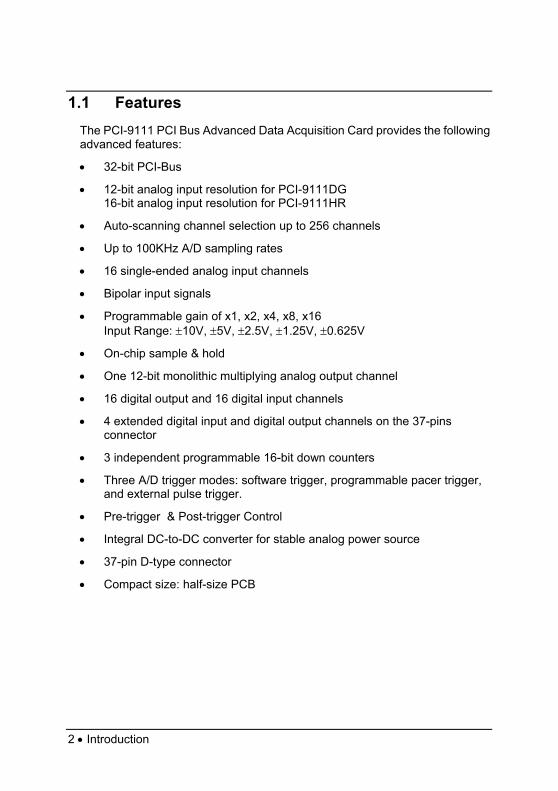
1.1 Features The PCI-9111 PCI Bus Advanced Data Acquisition Card provides the following advanced features:
• 32-bit PCI-Bus
• 12-bit analog input resolution for PCI-9111DG 16-bit analog input resolution for PCI-9111HR
• Auto-scanning channel selection up to 256 channels
• Up to 100KHz A/D sampling rates
• 16 single-ended analog input channels
• Bipolar input signals
• Programmable gain of x1, x2, x4, x8, x16 Input Range: ±10V, ±5V, ±2.5V, ±1.25V, ±0.625V
• On-chip sample & hold
• One 12-bit monolithic multiplying analog output channel
• 16 digital output and 16 digital input channels
• 4 extended digital input and digital output channels on the 37-pins connector
• 3 independent programmable 16-bit down counters
• Three A/D trigger modes: software trigger, programmable pacer trigger, and external pulse trigger.
• Pre-trigger & Post-trigger Control
• Integral DC-to-DC converter for stable analog power source
• 37-pin D-type connector
• Compact size: half-size PCB
Introduction • 3
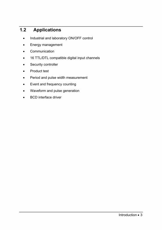
1.2 Applications • Industrial and laboratory ON/OFF control
• Energy management
• Communication
• 16 TTL/DTL compatible digital input channels
• Security controller
• Product test
• Period and pulse width measurement
• Event and frequency counting
• Waveform and pulse generation
• BCD interface driver
4 • Introduction
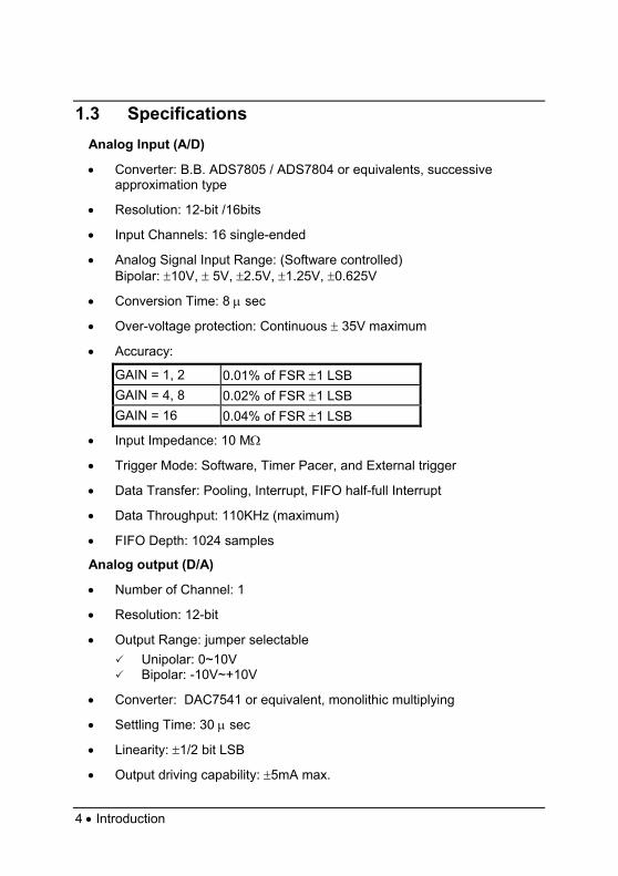
1.3 Specifications Analog Input (A/D)
• Converter: B.B. ADS7805 / ADS7804 or equivalents, successive approximation type
• Resolution: 12-bit /16bits
• Input Channels: 16 single-ended
• Analog Signal Input Range: (Software controlled) Bipolar: ±10V, ± 5V, ±2.5V, ±1.25V, ±0.625V
• Conversion Time: 8 µ sec
• Over-voltage protection: Continuous ± 35V maximum
• Accuracy:
GAIN = 1, 2 0.01% of FSR ±1 LSB GAIN = 4, 8 0.02% of FSR ±1 LSB GAIN = 16 0.04% of FSR ±1 LSB
• Input Impedance: 10 MΩ
• Trigger Mode: Software, Timer Pacer, and External trigger
• Data Transfer: Pooling, Interrupt, FIFO half-full Interrupt
• Data Throughput: 110KHz (maximum)
• FIFO Depth: 1024 samples
Analog output (D/A)
• Number of Channel: 1
• Resolution: 12-bit
• Output Range: jumper selectable Unipolar: 0~10V Bipolar: -10V~+10V
• Converter: DAC7541 or equivalent, monolithic multiplying
• Settling Time: 30 µ sec
• Linearity: ±1/2 bit LSB
• Output driving capability: ±5mA max.
Introduction • 5
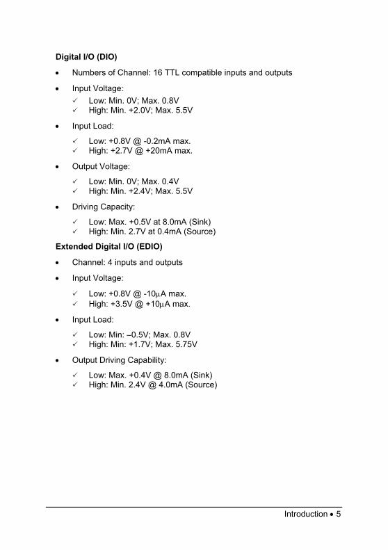
Digital I/O (DIO)
• Numbers of Channel: 16 TTL compatible inputs and outputs
• Input Voltage: Low: Min. 0V; Max. 0.8V High: Min. +2.0V; Max. 5.5V
• Input Load:
Low: +0.8V @ -0.2mA max. High: +2.7V @ +20mA max.
• Output Voltage:
Low: Min. 0V; Max. 0.4V High: Min. +2.4V; Max. 5.5V
• Driving Capacity:
Low: Max. +0.5V at 8.0mA (Sink) High: Min. 2.7V at 0.4mA (Source)
Extended Digital I/O (EDIO)
• Channel: 4 inputs and outputs
• Input Voltage:
Low: +0.8V @ -10µA max. High: +3.5V @ +10µA max.
• Input Load:
Low: Min: –0.5V; Max. 0.8V High: Min: +1.7V; Max. 5.75V
• Output Driving Capability:
Low: Max. +0.4V @ 8.0mA (Sink) High: Min. 2.4V @ 4.0mA (Source)
6 • Introduction
Programmable Counter
• Device: 8254
• A/D pacer: 32-bit timer (Two 16-bit counters cascaded together) with a 2MHz time base
• Pacer Output: 0.00046 Hz ~ 100 KHz
• Pre-trigger Counter: One 16-bit counter for counting AD Conversion Pulse
General Specifications
• Connector: 37-pin D-type connector
• Operating Temperature: 0°C ~ 60°C
• Storage Temperature: -20°C ~ 80°C
• Humidity: 5 ~ 95%, non-condensing
• Power Consumption: +5 V @ 570 mA typical
• Dimension: Compact size only 175mm x 105mm
Introduction • 7
1.4 Supporting Software ADLINK provides versatile software drivers and packages for users’ different approach to building a system. ADLINK not only provides programming libraries such as DLL for most Windows based systems, but also provide drivers for other software packages such as LabVIEW®, HP VEETM, DASYLabTM, InTouchTM, InControlTM, ISaGRAFTM, and so on.
All software options are included in the ADLINK CD. Non-free software drivers are protected with licensing codes. Without the software code, you can install and run the demo version for two hours for trial/demonstration purposes. Please contact ADLINK dealers to purchase the formal license
1.4.1 Programming Library For customers who are writing their own programs, we provide function libraries for many different operating systems, including:
• DOS Library: Borland C/C++ and Microsoft C++. Functional descriptions are included in this user’s guide.
• Windows 95 DLL: For VB, VC++, Delphi, and BC5. Functional descriptions are included in this user’s guide.
• PCIS-DASK: Include device drivers and DLL for Windows 98, Windows NT and Windows 2000. DLL is binary compatible across Windows 98, Windows NT and Windows 2000. That means all applications developed with PCIS-DASK are compatible across Windows 98, Windows NT and Windows 2000. The developing environment can be VB, VC++, Delphi, BC5, or any Windows programming language that allows calls to a DLL. The user’s guide and function reference manual of PCIS-DASK are in the CD. Please refer the PDF manual files under \\Manual_PDF\Software\PCIS-DASK
• PCIS-DASK/X: Include device drivers and shared libraries for Linux. The developing environment can be Gnu C/C++ or any programming language that allows linking to a shared library. The user’s guide and function reference manual of PCIS-DASK/X are in the CD. Please refer the PDF manual files under. (\Manual_PDF\Software\PCIS-DASK-X.)
The above software drivers are shipped with the board. Please refer to the “Software Installation Guide” for installation procedures.
8 • Introduction
1.4.2 PCIS-LVIEW: LabVIEW® Driver
PCIS-LVIEW contains the VIs, which is used to interface with NI’s LabVIEW® software package. The PCIS-LVIEW supports Windows 95/98/NT/2000. The LabVIEW® drivers is shipped free with the board. You can install and use them without a license. For more information about PCIS-LVIEW, please refer to the user’s guide in the CD. (\\Manual_PDF\Software\PCIS-LVIEW)
1.4.3 PCIS-VEE: HP-VEE Driver The PCIS-VEE includes user objects, which are used to interface with HP’s VEE software package. PCIS-VEE supports Windows 95/98/NT. The HP-VEE drivers are shipped free with the board. You can install and use them without a license. For more information about PCIS-VEE, please refer to the user’s guide in the CD. (\\Manual_PDF\Software\PCIS-VEE)
1.4.4 DAQBenchTM: ActiveX Controls We suggest customers who are familiar with ActiveX controls and VB/VC++ programming use the DAQBenchTM ActiveX Control component library for developing applications. The DAQBenchTM is designed under Windows NT/98. For more information about DAQBench, please refer to the user’s guide in the CD. (\\Manual_PDF\Software\DAQBench\DAQBench Manual.PDF)
1.4.5 DASYLabTM PRO DASYLab is an easy-to-use software package, which provides easy-setup instrument functions such as FFT analysis. Please contact ADLINK to purchase a copy of DASYLab PRO, which includes DASYLab and ADLINK hardware drivers.
1.4.6 PCIS-DDE: DDE Server and InTouchTM DDE stands for Dynamic Data Exchange. The PCIS-DDE includes the PCI cards’ DDE server. The PCIS-DDE server is included in the ADLINK CD. It needs a license. The DDE server can be used in conjunction with any DDE client under Windows NT.
1.4.7 PCIS-ISG: ISaGRAFTM driver The ISaGRAF WorkBench is an IEC1131-3 SoftPLC control program development environment. The PCIS-ISG includes ADLINK product drivers for ISaGRAF under Windows NT environment. The PCIS-ISG is included in the ADLINK CD. A license is needed to use the drivers.

Introduction • 9
1.4.8 PCIS-ICL: InControlTM Driver PCIS-ICL is the InControl driver, which supports Windows NT. The PCIS-ICL is included in the ADLINK CD. A license is needed to use the drivers.
1.4.9 PCIS-OPC: OPC Server PCIS-OPC is an OPC Server, which can link with OPC clients. There are several software packages on the market, which can provide the OPC clients. The PCIS-OPC supports Windows NT and requires a license to operate.
10 • Installation
2
Installation
This chapter describes how to install the PCI-9111. Follow the steps carefully.
• Check what you have (section 2.1)
• Unpacking (section 2.2)
• Check the PCB and jumper locations (section 2.3)
• Setup jumpers (section 2.4)
• Installing the hardware (section 2.5)
• Installing the software drivers for windows (section 2.6)
• Daughter Board connections (section 2.8)
The PCI-9111 automatically configures the IRQ, port and BIOS addresses. Therefore, it is not necessary to configure these addresses, hence avoiding any addressing conflicts.

Installation • 11
2.1 What You Have In addition to this User's Guide, the package should include the following items:
PCI-9111 Enhanced Multi-function Data Acquisition Card
ADLINK CD
Software Installation Guide
If any of these items are missing or damaged, contact the dealer from whom you purchased the product. Save the shipping materials and carton in case you want to ship or store the product in the future.
2.2 Unpacking The card contains electro-static sensitive components that can be easily be damaged by static electricity.
Therefore, the card should be handled on a grounded anti-static mat. The operator should be wearing an anti-static wristband, grounded at the same point as the anti-static mat.
Inspect the card module carton for obvious damages. Shipping and handling may cause damage to your module. Be sure there are no shipping and handling damages on the modules carton before continuing.
After opening the card module carton, extract the system module and place it only on a grounded anti-static surface with component side up.
Again, inspect the module for damages. Press down on all the socketed IC's to make sure that they are properly seated. Do this only with the module place on a firm flat surface.
Note: DO NOT ATTEMPT TO INSTALL A DAMAGED BOARD IN THE COMPUTER.
You are now ready to install your card.
12 • Installation
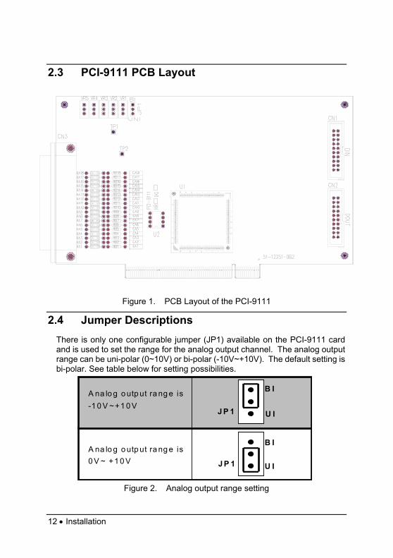
2.3 PCI-9111 PCB Layout
Figure 1. PCB Layout of the PCI-9111
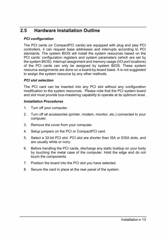
2.4 Jumper Descriptions There is only one configurable jumper (JP1) available on the PCI-9111 card and is used to set the range for the analog output channel. The analog output range can be uni-polar (0~10V) or bi-polar (-10V~+10V). The default setting is bi-polar. See table below for setting possibilities.
A na lo g o utp ut ra ng e is -1 0 V ~+1 0 V
A na lo g o utp ut ra ng e is 0 V ~ +1 0 V
U I
B I
J P 1
U I
B I
J P 1
Figure 2. Analog output range setting
Installation • 13
2.5 Hardware Installation Outline PCI configuration
The PCI cards (or CompactPCI cards) are equipped with plug and play PCI controllers, it can request base addresses and interrupts according to PCI standards. The system BIOS will install the system resources based on the PCI cards’ configuration registers and system parameters (which are set by the system BIOS). Interrupt assignment and memory usage (I/O port locations) of the PCI cards can only be assigned by system BIOS. These system resource assignments are done on a board-by-board basis. It is not suggested to assign the system resource by any other methods.
PCI slot selection
The PCI card can be inserted into any PCI slot without any configuration modification to the system resources. Please note that the PCI system board and slot must provide bus-mastering capability to operate at its optimum level.
Installation Procedures
1. Turn off your computer.
2. Turn off all accessories (printer, modem, monitor, etc.) connected to your computer.
3. Remove the cover from your computer.
4. Setup jumpers on the PCI or CompactPCI card.
5. Select a 32-bit PCI slot. PCI slot are shorter than ISA or EISA slots, and are usually white or ivory.
6. Before handling the PCI cards, discharge any static buildup on your body by touching the metal case of the computer. Hold the edge and do not touch the components.
7. Position the board into the PCI slot you have selected.
8. Secure the card in place at the rear panel of the system.
14 • Installation
2.6 Device Installation for Windows Systems Once Windows 95/98/2000 has started, the Plug and Play function of Windows system will find the new NuDAQ/NuIPC cards. If this is the first time the NuDAQ/NuIPC cards are running on your Windows system, you will be prompted to input the device information source. Please refer to the “Software Installation Guide” for step-by-step installation procedures.
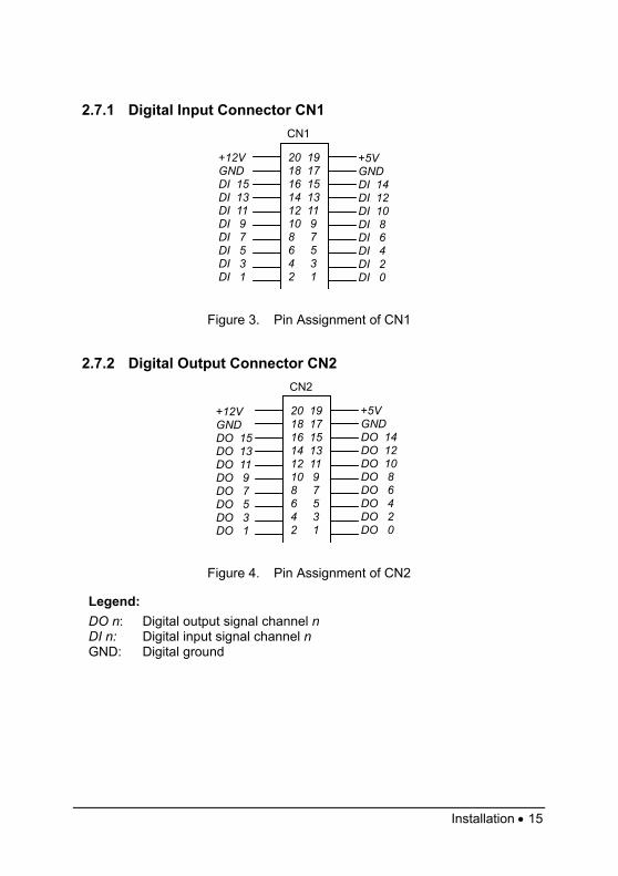
2.7 Connectors Pin Assignment The PCI-9111 comes equipped with two 20-pin insulation displacement connectors - CN1 and CN2 and one 37-pin D-type connector - CN3. CN1 and CN2 are located on board with CN3 located at the rear plate.
CN1 is used for digital input signals, CN2 for digital output signals and CN3 for analog input and output, extended digital I/O and timer/counter signals. Pin assignments for each connector is illustrated in Figure 3 ~ Figure 5.
Installation • 15
2.7.1 Digital Input Connector CN1
+5V GND DI 14 DI 12 DI 10 DI 8 DI 6 DI 4 DI 2 DI 0
CN1
+12V GND DI 15 DI 13 DI 11 DI 9 DI 7 DI 5 DI 3 DI 1
20 1918 1716 1514 1312 1110 98 76 54 32 1
Figure 3. Pin Assignment of CN1
2.7.2 Digital Output Connector CN2
+5V GND DO 14DO 12DO 10DO 8DO 6DO 4DO 2DO 0
CN2
+12V GND DO 15DO 13DO 11DO 9DO 7DO 5DO 3DO 1
20 1918 1716 1514 1312 1110 98 76 54 32 1
Figure 4. Pin Assignment of CN2
Legend: DO n: Digital output signal channel n DI n: Digital input signal channel n GND: Digital ground
16 • Installation
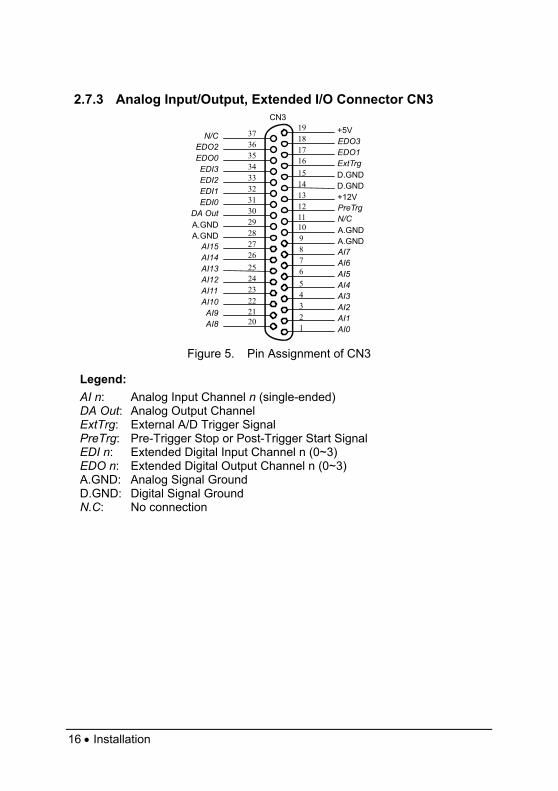
2.7.3 Analog Input/Output, Extended I/O Connector CN3
AI2
12345678910111213141516171819
21222324252627282930
20
31323334353637
AI3AI10AI9AI8
AI1AI0
AI6AI7
AI5AI4
AI13AI14
AI12AI11
DA Out
A.GNDAI15 A.GND
A.GND A.GND
D.GND+12V
D.GND
+5V
ExtTrg
CN3
N/CPreTrg
N/C
EDO0EDO1EDO2EDO3
EDI0EDI1EDI2EDI3
Figure 5. Pin Assignment of CN3
Legend: AI n: Analog Input Channel n (single-ended) DA Out: Analog Output Channel ExtTrg: External A/D Trigger Signal PreTrg: Pre-Trigger Stop or Post-Trigger Start Signal EDI n: Extended Digital Input Channel n (0~3) EDO n: Extended Digital Output Channel n (0~3) A.GND: Analog Signal Ground D.GND: Digital Signal Ground N.C: No connection
Installation • 17
2.8 Daughter Board Connection The PCI-9111 can be connected with five different daughter boards. The following are compatible: ACLD-8125, 9137, 9138, 9182, 9185, and 9188. The functionality and connections are specified in the following sections
2.8.1 Connect with ACLD-8125 The ACLD-8125 has a 37-pin D-sub connector, which can connect to the PCI-9111 through the 37-pin assemble cable. The most outstanding feature of this daughter board is the CJC (cold junction compensation) circuit on board. You can directly connect a thermocouple to the ACL-8125 board. The CJC is only suitable for High Gain version boards
2.8.2 Connect with ACLD-9137 The ACLD-9137 is directly connected to the cards’ 37-pin D-sub connector. It is suitable for simple applications that do not need complex signal conditioning before an A/D conversion is performed.
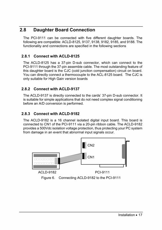
2.8.3 Connect with ACLD-9182 The ACLD-9182 is a 16 channel isolated digital input board. This board is connected to CN1 of the PCI-9111 via a 20-pin ribbon cable. The ACLD-9182 provides a 500Vdc isolation voltage protection, thus protecting your PC system from damage in an event that abnormal input signals occur.
Figure 6. Connecting ACLD-9182 to the PCI-9111 PCI-9111ACLD-9182
CN1 CN2
18 • Installation
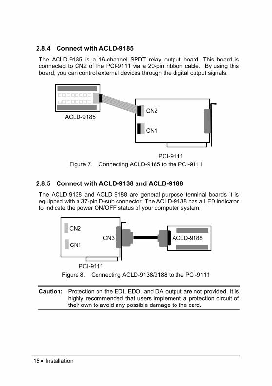
2.8.4 Connect with ACLD-9185 The ACLD-9185 is a 16-channel SPDT relay output board. This board is connected to CN2 of the PCI-9111 via a 20-pin ribbon cable. By using this board, you can control external devices through the digital output signals.
Figure 7. Connecting ACLD-9185 to the PCI-9111
2.8.5 Connect with ACLD-9138 and ACLD-9188 The ACLD-9138 and ACLD-9188 are general-purpose terminal boards it is equipped with a 37-pin D-sub connector. The ACLD-9138 has a LED indicator to indicate the power ON/OFF status of your computer system.
Figure 8. Connecting ACLD-9138/9188 to the PCI-9111
Caution: Protection on the EDI, EDO, and DA output are not provided. It is highly recommended that users implement a protection circuit of their own to avoid any possible damage to the card.
ACLD-9185
PCI-9111
CN1 CN2
ACLD-9188
PCI-9111
CN2
CN1CN3

Registers • 19
3
Registers
The descriptions of the registers and structure of the PCI-9111 are outlined in this chapter. The information in this chapter will assist programmers wishing to handle the card with low-level programs.
In addition, the low level programming syntax is introduced. This will help beginners learn how to operate the PCI-9111 in the shortest possible time.
20 • Registers
3.1 PCI PnP Registers The PCI-9111 functions as a 32-bit PCI target device to any master on the PCI bus. It supports burst transfer to memory space by using 32-bit data. All data read and write is base on 32-bit data. There are three types of registers on the PCI-9111: The PCI Configuration Registers (PCR), Local Configuration Registers (LCR) and the 9111 registers.
The PCR is compliant to the PCI-bus specifications. It is initialized and controlled by the plug & play (PnP) PCI BIOS. User can study the PCI BIOS specification to understand the operation of the PCR. Please contact PCISIG to acquire the specifications of the PCI interface.
The PCI bus controller (PCI-9050) is provided by PLX technology Inc. (www.plxtech.com). For more detailed information of the LCR, please visit PLX technology’s web site. It is not necessary for users to fully understand in detail the LCR if the software library is used. The PCI PnP BIOS assigns the base address of the LCR. The assigned address is located at 14h of PCR.
The PCI-9111 registers are shown in the next section. The base address, which is also assigned by the PCI PnP BIOS, is located at an offset of 18h of the PCR. Do not try to modify the base address and interrupt which is assigned by the PCI PnP BIOS; it may cause resource conflicts in your system.
Registers • 21
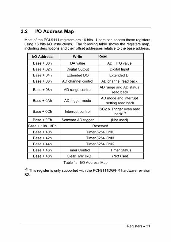
3.2 I/O Address Map Most of the PCI-9111 registers are 16 bits. Users can access these registers using 16 bits I/O instructions. The following table shows the registers map, including descriptions and their offset addresses relative to the base address.
I/O Address Write Read
Base + 00h DA value AD FIFO value Base + 02h Digital Output Digital Input Base + 04h Extended DO Extended DI Base + 06h AD channel control AD channel read back
Base + 08h AD range control AD range and AD status
read back
Base + 0Ah AD trigger mode AD mode and interrupt
setting read back
Base + 0Ch Interrupt control ISC2 & Trigger even read
back*1) Base + 0Eh Software AD trigger (Not used)
Base + 10h ~3Eh Reserved Base + 40h Timer 8254 Ch#0 Base + 42h Timer 8254 Ch#1 Base + 44h Timer 8254 Ch#2
Base + 46h Timer Control Timer Status Base + 48h Clear H/W IRQ (Not used)
Table 1: I/O Address Map
*1) This register is only supported with the PCI-9111DG/HR hardware revision B2.
22 • Registers
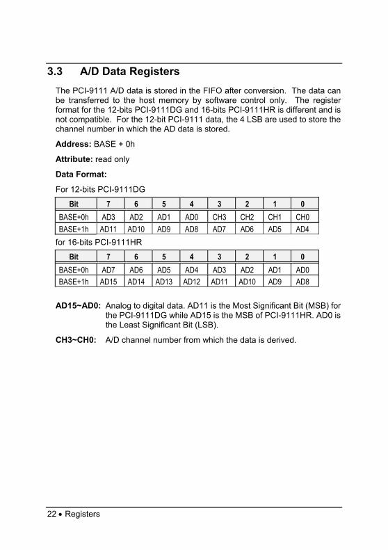
3.3 A/D Data Registers The PCI-9111 A/D data is stored in the FIFO after conversion. The data can be transferred to the host memory by software control only. The register format for the 12-bits PCI-9111DG and 16-bits PCI-9111HR is different and is not compatible. For the 12-bit PCI-9111 data, the 4 LSB are used to store the channel number in which the AD data is stored.
Address: BASE + 0h
Attribute: read only
Data Format:
For 12-bits PCI-9111DG
Bit 7 6 5 4 3 2 1 0 BASE+0h AD3 AD2 AD1 AD0 CH3 CH2 CH1 CH0 BASE+1h AD11 AD10 AD9 AD8 AD7 AD6 AD5 AD4
for 16-bits PCI-9111HR
Bit 7 6 5 4 3 2 1 0 BASE+0h AD7 AD6 AD5 AD4 AD3 AD2 AD1 AD0 BASE+1h AD15 AD14 AD13 AD12 AD11 AD10 AD9 AD8
AD15~AD0: Analog to digital data. AD11 is the Most Significant Bit (MSB) for
the PCI-9111DG while AD15 is the MSB of PCI-9111HR. AD0 is the Least Significant Bit (LSB).
CH3~CH0: A/D channel number from which the data is derived.
Registers • 23
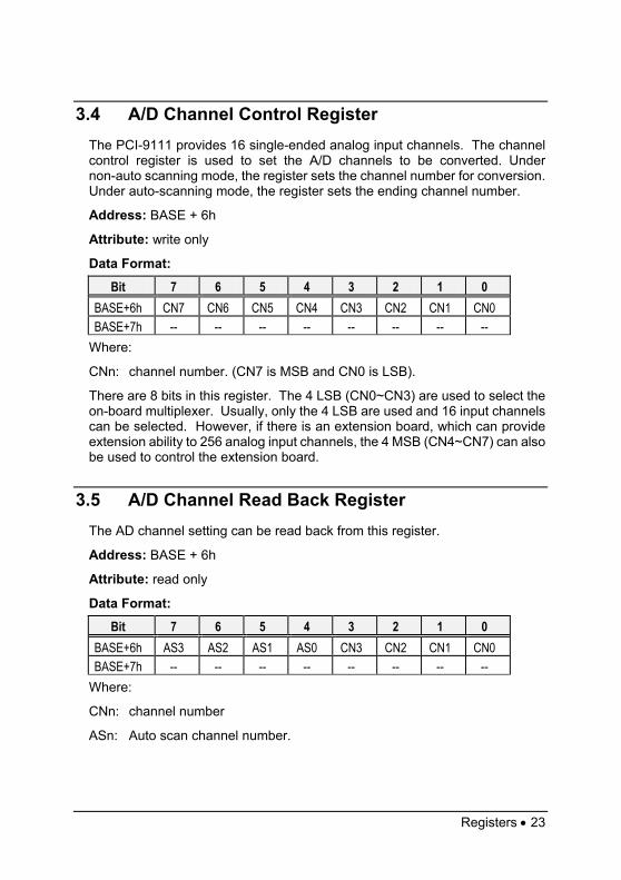
3.4 A/D Channel Control Register The PCI-9111 provides 16 single-ended analog input channels. The channel control register is used to set the A/D channels to be converted. Under non-auto scanning mode, the register sets the channel number for conversion. Under auto-scanning mode, the register sets the ending channel number.
Address: BASE + 6h
Attribute: write only
Data Format:
Bit 7 6 5 4 3 2 1 0 BASE+6h CN7 CN6 CN5 CN4 CN3 CN2 CN1 CN0 BASE+7h -- -- -- -- -- -- -- --
Where:
CNn: channel number. (CN7 is MSB and CN0 is LSB).
There are 8 bits in this register. The 4 LSB (CN0~CN3) are used to select the on-board multiplexer. Usually, only the 4 LSB are used and 16 input channels can be selected. However, if there is an extension board, which can provide extension ability to 256 analog input channels, the 4 MSB (CN4~CN7) can also be used to control the extension board.
3.5 A/D Channel Read Back Register The AD channel setting can be read back from this register.
Address: BASE + 6h
Attribute: read only
Data Format:
Bit 7 6 5 4 3 2 1 0 BASE+6h AS3 AS2 AS1 AS0 CN3 CN2 CN1 CN0 BASE+7h -- -- -- -- -- -- -- --
Where:
CNn: channel number
ASn: Auto scan channel number.
24 • Registers
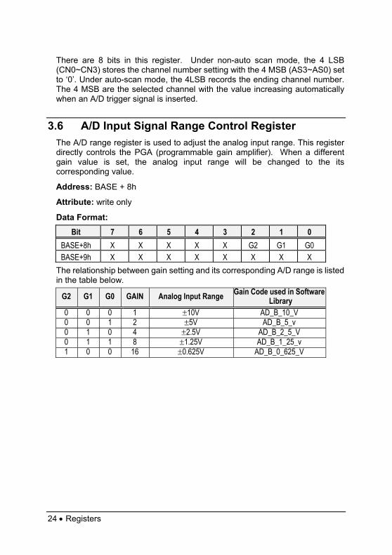
There are 8 bits in this register. Under non-auto scan mode, the 4 LSB (CN0~CN3) stores the channel number setting with the 4 MSB (AS3~AS0) set to ‘0’. Under auto-scan mode, the 4LSB records the ending channel number. The 4 MSB are the selected channel with the value increasing automatically when an A/D trigger signal is inserted.
3.6 A/D Input Signal Range Control Register The A/D range register is used to adjust the analog input range. This register directly controls the PGA (programmable gain amplifier). When a different gain value is set, the analog input range will be changed to the its corresponding value.
Address: BASE + 8h
Attribute: write only
Data Format:
Bit 7 6 5 4 3 2 1 0 BASE+8h X X X X X G2 G1 G0 BASE+9h X X X X X X X X
The relationship between gain setting and its corresponding A/D range is listed in the table below.
G2 G1 G0 GAIN Analog Input Range Gain Code used in Software Library
0 0 0 1 ±10V AD_B_10_V 0 0 1 2 ±5V AD_B_5_v 0 1 0 4 ±2.5V AD_B_2_5_V 0 1 1 8 ±1.25V AD_B_1_25_v 1 0 0 16 ±0.625V AD_B_0_625_V
Registers • 25
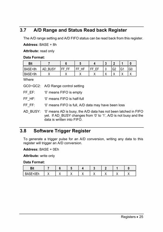
3.7 A/D Range and Status Read back Register The A/D range setting and A/D FIFO status can be read back from this register.
Address: BASE + 8h
Attribute: read only
Data Format:
Bit 7 6 5 4 3 2 1 0 BASE+8h AD_BUSY FF_FF FF_HF FF_EF 0 G2 G1 G0 BASE+9h X X X X X X X X Where
GC0~GC2: A/D Range control setting
FF_EF: ‘0’ means FIFO is empty
FF_HF: ‘0’ means FIFO is half-full
FF_FF: ‘0’ means FIFO is full, A/D data may have been loss
AD_BUSY: ‘0’ means AD is busy, the A/D data has not been latched in FIFO yet. If AD_BUSY changes from ‘0’ to ‘1’, A/D is not busy and the data is written into FIFO.
3.8 Software Trigger Register To generate a trigger pulse for an A/D conversion, writing any data to this register will trigger an A/D conversion.
Address: BASE + 0Eh
Attribute: write only
Data Format:
Bit 7 6 5 4 3 2 1 0 BASE+0Eh X X X X X X X X

26 • Registers
3.9 A/D Trigger Mode Control Register This register is used to control the A/D trigger source and trigger method.
Address: BASE + 0Ah
Attribute: write only
Data Format:
Bit 7 6 5 4 3 2 1 0 BASE+0Ah X X TRGEVENT POTRG PTRG EITS TPST ASCAN BASE+0Bh X X X X X X X X
TRGEVENT: Post / Pre-rigger event flag clear, write 1 to clear the trigger event
POTRG: Post-trigger ON/OFF control 0: Post-trigger OFF 1: Post-Trigger ON
PTRG: Pre-trigger ON/OFF control 0: Pre-trigger OFF 1: Pre-Trigger ON
EITS: External / Internal Trigger Source 1: External Trigger Source 0: Internal Trigger Source
TPST: Timer Pacer/ Software Trigger 0: Software Trigger 1: Timer Pacer Trigger
ASCAN: Auto Scan Control 0: Auto Scan OFF 1: Auto Scan ON
Only the modes listed below applied on the PCI-9111 card:
Bit 4 POTRG (Note 2)
Bit 3 PTRG
Bit 2 EITS
Bit 1 TPST
Bit 0 ASCAN Mode Description (Note 1)
0/1 0/1 0 0 0/1 Software Trigger & Polling 0/1 0/1 0 1 0/1 Timer Pacer Trigger 0/1 0/1 1 X 0/1 External Trigger
Registers • 27
Note 1: The bits in this register can only control the A/D trigger source and trigger method. The trigger conditions are independent from data transfer method and interrupt generation.
Note 2: The setting of Pre-trigger and Post-trigger in bit 3 & 4 are exclusive. There is only one mode can be enabled at one time
Note 3: TRGEVENT and POTRG bits support for hardware revision B2. It’s not available in old version.
3.10 Interrupt Control Register The PCI-9111 has a dual interrupt system, thus two interrupt sources can be generated and can be checked using the software. This register is used to select the interrupt source.
Address: BASE + 0Ch
Attribute: write only
Data Format:
Bit 7 6 5 4 3 2 1 0 BASE+0Ch X X X X ISC2 FFEN ISC1 ISC0
ISC0: IRQ0 signal select
0: IRQ on the ending of the AD conversion (EOC)
1: IRQ when FIFO is half full
ISC2 ISC1 IRQ1 signal select
0 0 IRQ every Timer tick
0 1 IRQ when ExtTrg signal changes from ‘H’ to ‘L’
1 0 IRQ when pre-trigger counter is counting down to 0
FFEN: FIFO enable pin
0: FIFO Enable (Power On Default value)
1: FIFO Disable
(To reset the FIFO, set FFEN sequence as 0 -> 1 -> 0)
Note 1: ISC2 control bit is only supported with hardware version B2, i.e. An IRQ is available when the pre-trigger counter is counting down.
28 • Registers
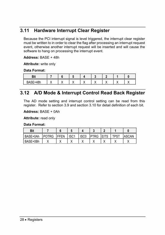
3.11 Hardware Interrupt Clear Register Because the PCI interrupt signal is level triggered, the interrupt clear register must be written to in order to clear the flag after processing an interrupt request event, otherwise another interrupt request will be inserted and will cause the software to hang on processing the interrupt event.
Address: BASE + 48h
Attribute: write only
Data Format:
Bit 7 6 5 4 3 2 1 0 BASE+48h X X X X X X X X
3.12 A/D Mode & Interrupt Control Read Back Register The AD mode setting and interrupt control setting can be read from this register. Refer to section 3.9 and section 3.10 for detail definition of each bit.
Address: BASE + 0Ah
Attribute: read only
Data Format:
Bit 7 6 5 4 3 2 1 0 BASE+0Ah POTRG FFEN ISC1 ISC0 PTRG EITS TPST ASCAN BASE+0Bh X X X X X X X X
Registers • 29
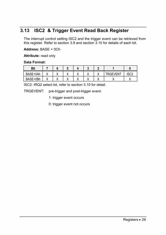
3.13 ISC2 & Trigger Event Read Back Register The interrupt control setting ISC2 and the trigger event can be retrieved from this register. Refer to section 3.9 and section 3.10 for details of each bit.
Address: BASE + 0Ch
Attribute: read only
Data Format:
Bit 7 6 5 4 3 2 1 0 BASE+0Ah X X X X X X TRGEVENT ISC2 BASE+0Bh X X X X X X X X
ISC2: IRQ2 select bit, refer to section 3.10 for detail.
TRGEVENT: pre-trigger and post-trigger event.
1: trigger event occurs
0: trigger event not occurs
30 • Registers
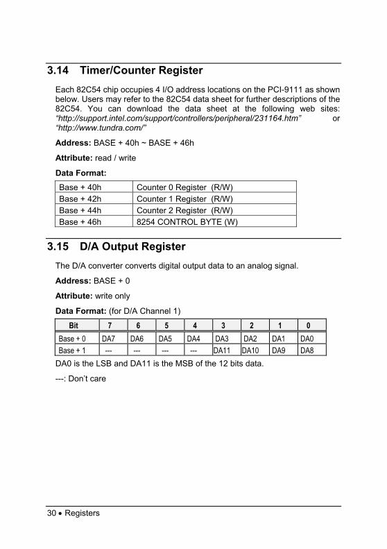
3.14 Timer/Counter Register Each 82C54 chip occupies 4 I/O address locations on the PCI-9111 as shown below. Users may refer to the 82C54 data sheet for further descriptions of the 82C54. You can download the data sheet at the following web sites: “http://support.intel.com/support/controllers/peripheral/231164.htm” or “http://www.tundra.com/”
Address: BASE + 40h ~ BASE + 46h
Attribute: read / write
Data Format: Base + 40h Counter 0 Register (R/W) Base + 42h Counter 1 Register (R/W) Base + 44h Counter 2 Register (R/W) Base + 46h 8254 CONTROL BYTE (W)
3.15 D/A Output Register The D/A converter converts digital output data to an analog signal.
Address: BASE + 0
Attribute: write only
Data Format: (for D/A Channel 1)
Bit 7 6 5 4 3 2 1 0 Base + 0 DA7 DA6 DA5 DA4 DA3 DA2 DA1 DA0 Base + 1 --- --- --- --- DA11 DA10 DA9 DA8
DA0 is the LSB and DA11 is the MSB of the 12 bits data.
---: Don’t care
Registers • 31
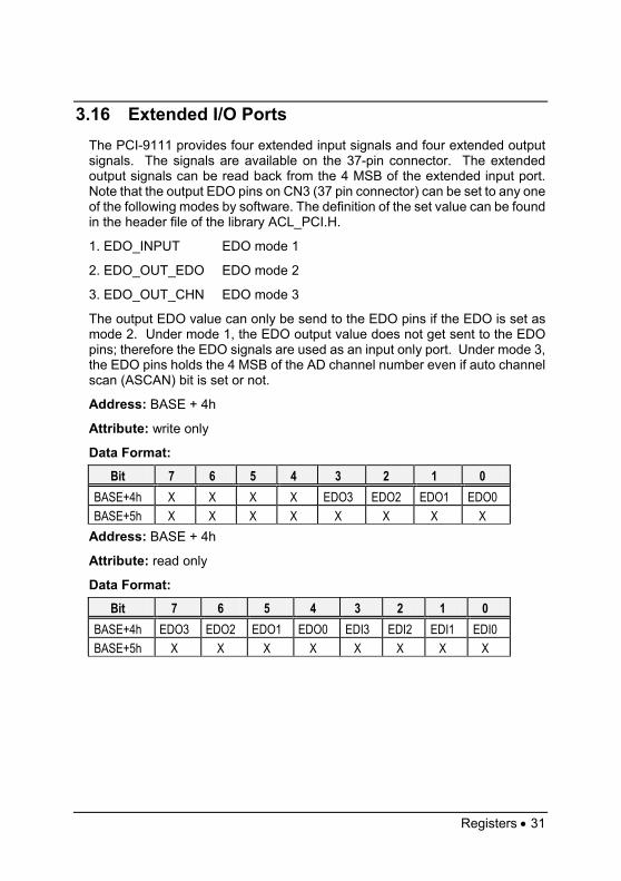
3.16 Extended I/O Ports The PCI-9111 provides four extended input signals and four extended output signals. The signals are available on the 37-pin connector. The extended output signals can be read back from the 4 MSB of the extended input port. Note that the output EDO pins on CN3 (37 pin connector) can be set to any one of the following modes by software. The definition of the set value can be found in the header file of the library ACL_PCI.H.
1. EDO_INPUT EDO mode 1
2. EDO_OUT_EDO EDO mode 2
3. EDO_OUT_CHN EDO mode 3
The output EDO value can only be send to the EDO pins if the EDO is set as mode 2. Under mode 1, the EDO output value does not get sent to the EDO pins; therefore the EDO signals are used as an input only port. Under mode 3, the EDO pins holds the 4 MSB of the AD channel number even if auto channel scan (ASCAN) bit is set or not.
Address: BASE + 4h
Attribute: write only
Data Format:
Bit 7 6 5 4 3 2 1 0 BASE+4h X X X X EDO3 EDO2 EDO1 EDO0 BASE+5h X X X X X X X X
Address: BASE + 4h
Attribute: read only
Data Format:
Bit 7 6 5 4 3 2 1 0 BASE+4h EDO3 EDO2 EDO1 EDO0 EDI3 EDI2 EDI1 EDI0 BASE+5h X X X X X X X X
32 • Registers
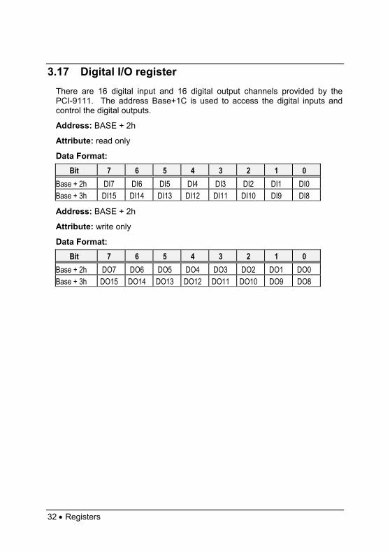
3.17 Digital I/O register There are 16 digital input and 16 digital output channels provided by the PCI-9111. The address Base+1C is used to access the digital inputs and control the digital outputs.
Address: BASE + 2h
Attribute: read only
Data Format:
Bit 7 6 5 4 3 2 1 0 Base + 2h DI7 DI6 DI5 DI4 DI3 DI2 DI1 DI0 Base + 3h DI15 DI14 DI13 DI12 DI11 DI10 DI9 DI8
Address: BASE + 2h
Attribute: write only
Data Format:
Bit 7 6 5 4 3 2 1 0 Base + 2h DO7 DO6 DO5 DO4 DO3 DO2 DO1 DO0 Base + 3h DO15 DO14 DO13 DO12 DO11 DO10 DO9 DO8
Operation Theory • 33
4
Operation Theory
The operation theory of the functions on PCI-9111 card is described in this chapter. The functions include the A/D conversion, D/A conversion, Digital I/O and counter / timer. The operation theory can help users understand how to configure or to program the PCI-9111.
4.1 A/D Conversion Before programming the PCI-9111 to perform any A/D conversions, you should understand the following issues:
• A/D conversion procedure
• A/D signal source control
• A/D trigger source control
• A/D data transfer mode
• A/D Pre-trigger function
• Interrupt System (refer to section 4.2)
• A/D data format
Note: Because some A/D data transfer modes will utilizes the systems interrupt resources, users also need a basic understanding the interrupt system (section 4.2).
34 • Operation Theory
4.1.1 A/D Conversion Procedure To use the A/D converter, users first need to know the properties of the signal being measured. Users then can decide on which channels to use on the PCI-9111. Refer to section 2.7 ‘Connectors Pin Assignment’. In addition, users need to define and control the A/D signal sources, including the A/D channel, A/D gain, and A/D signal types. Refer to section 4.1.2. For A/D signal source control.
After deciding on the A/D signal source, users must decide how to trigger the A/D conversion and define/control the trigger source. The A/D converter will start to convert analog signals to a digital value when a trigger signal is on a rising edge. Refer to the section 4.1.3 for all possible trigger modes.
The A/D data should be transferred to the PC's memory for further processing is required. The data can be read either by an I/O instruction set, which is handled directly by software or transferred to memory via an interrupt routine. Refer to section 4.1.4 for more information regarding multi-configurations for the A/D data transfer process.
Some applications may require obtaining the data only before or after special hardware event. The Pre-Trigger is useful to stop the A/D operation. Refer to section 4.1.5 for configuring the PCI-9111 for Pre-Trigger Mode.
To process the A/D data, programmer should have n understanding of the A/D data format. Refer to section 4.1.6 for details.
4.1.2 A/D Signal Source Control To control the A/D signal source, the signal type, signal channel and signal range should be considered.
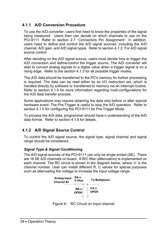
Signal Type & Signal Conditioning The A/D signal sources of the PCI-9111 can only be single ended (SE). There are 16 SE A/D channels on board. A R/C filter (attenuators) is implemented on each channel. The RC circuit is shown in the diagram below, where ‘n’ is the channel number. User can install different R, C values for special purposes such as attenuating the voltage to increase the input voltage range.
Figure 9. RC Circuit on Input channel
RA n0 Ohm To MultiplexerAnalog Input
Channel #n
RB nOPEN
CA n OPEN
Operation Theory • 35
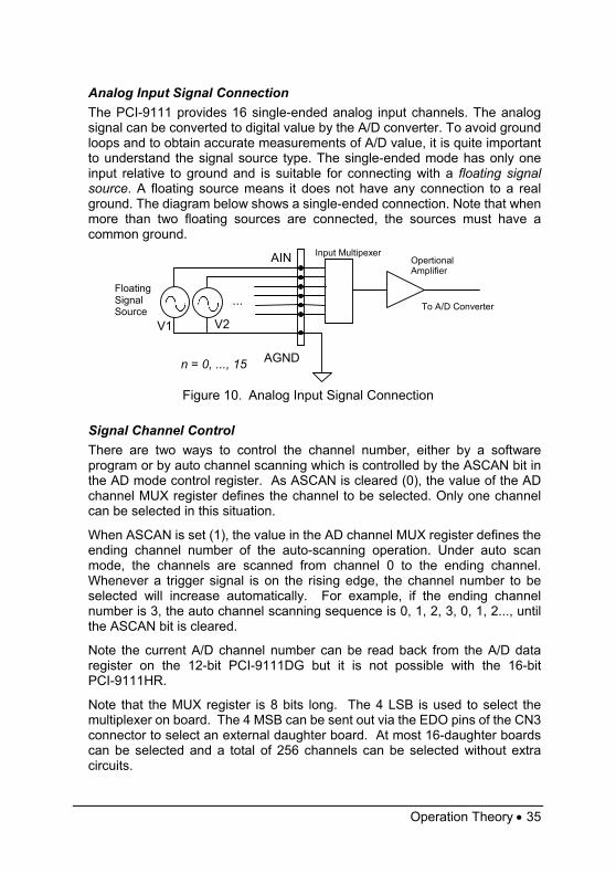
Analog Input Signal Connection The PCI-9111 provides 16 single-ended analog input channels. The analog signal can be converted to digital value by the A/D converter. To avoid ground loops and to obtain accurate measurements of A/D value, it is quite important to understand the signal source type. The single-ended mode has only one input relative to ground and is suitable for connecting with a floating signal source. A floating source means it does not have any connection to a real ground. The diagram below shows a single-ended connection. Note that when more than two floating sources are connected, the sources must have a common ground.
Figure 10. Analog Input Signal Connection
Signal Channel Control There are two ways to control the channel number, either by a software program or by auto channel scanning which is controlled by the ASCAN bit in the AD mode control register. As ASCAN is cleared (0), the value of the AD channel MUX register defines the channel to be selected. Only one channel can be selected in this situation.
When ASCAN is set (1), the value in the AD channel MUX register defines the ending channel number of the auto-scanning operation. Under auto scan mode, the channels are scanned from channel 0 to the ending channel. Whenever a trigger signal is on the rising edge, the channel number to be selected will increase automatically. For example, if the ending channel number is 3, the auto channel scanning sequence is 0, 1, 2, 3, 0, 1, 2..., until the ASCAN bit is cleared.
Note the current A/D channel number can be read back from the A/D data register on the 12-bit PCI-9111DG but it is not possible with the 16-bit PCI-9111HR.
Note that the MUX register is 8 bits long. The 4 LSB is used to select the multiplexer on board. The 4 MSB can be sent out via the EDO pins of the CN3 connector to select an external daughter board. At most 16-daughter boards can be selected and a total of 256 channels can be selected without extra circuits.
AIN
AGND n = 0, ..., 15
Floating Signal Source
Opertional Amplifier
To A/D Converter
Input Multipexer
...
V1 V2
36 • Operation Theory
Signal Range A properly define signal range is important in any data acquisition process. The input signal may be saturated if the A/D gain is too large or the resolution may be not enough if the signal is small. The maximum A/D signal range of the PCI-9111 is +/- 10 volts when the A/D gain value is 1. The A/D gain control register controls the maximum signal input range. The signal gain is programmable with 5 levels (1, 2, 4, 8, 16). The signal ranges of the 16 channels are identical at all times.
The available signal polarity on PCI-9111 is bi-polar. However, the bi-polar input range can still cover a uni-polar application. In addition the high resolution of the PCI-9111HR can cover most applications.
4.1.3 A/D Trigger Source Control An A/D conversion is started when a trigger signal is detected. With the PCI-9111, an A/D conversion can be triggered by either an Internal or External trigger source. The EITS bit of the A/D control register is used to handle an internal or external trigger. Refer to section 3.9 for details. Whenever an external source is set, the internal sources are disabled.
If an internal trigger is selected, two internal sources can be selected, either software or timer pacer trigger. The A/D bits EITS and TPST of the A/D mode register controls the A/D operations mode. There are 3 different trigger conditions available to the PCI-9111. The different trigger conditions are specified below:
Software trigger (EITS=0, TPST=0) The trigger source is software controllable in this mode. That is, the A/D conversion is started when any value is written into the software trigger register. This trigger mode is suitable for low speed A/D conversions. Under this mode, the timing of the A/D conversion is fully controlled by the software. However, it is difficult to control a fixed A/D conversion rate unless another timer interrupt service routine is used to generate a fixed rate trigger. Refer to the interrupt control section for fixed rate timer interrupt.
Timer Pacer Trigger (EITS=0, TPST=1) The on-board timer/counter chip 8254 is used to provide a trigger source for an A/D conversion at a fixed rate. Two counters of the 8254 chip are cascaded together to generate a trigger pulse at precise periods. Refer to section 4.6 for timer/counter operations. This mode is ideal for high speed A/D conversion. It can be combined with the FIFO half full interrupt or EOC interrupt to transfer data. The A/D trigger, A/D data transfer and Interrupt can be set independently, thus most complex applications can be covered.
Operation Theory • 37
It's recommended that this mode be used if the application requires a fixed and precise A/D sampling rate.
External Trigger (EITS=1, TPST=don‘t care) Through pin-16 of CN3 (ExtTrig), an A/D conversion can also be triggered by an external signal. The A/D conversion starts when ExtTrig changes from a high to a low level. The conversion rate in this mode is more flexible depending on the available trigger options of the external device. The external trigger can be also combined with the FIFO half interrupt, EOC interrupt or program FIFO polling for transferring data.
4.1.4 A/D Data Transfer Modes The A/D data are buffered in the FIFO memory. The FIFO size of the PCI-9111 is 1024 (1K) words. If the sampling rate is 100 KHz, the FIFO can buffer 10.24 ms of analog signal. Data transferred to the FIFO after the FIFO is full will be lost. The software must read out the FIFO data before it becomes full.
The data must be transferred to the host memory after the data is ready and before the FIFO is full. With the PCI-9111, Different transfer modes can be used. The different transfer modes are described below:
Software Data Polling The software data polling is the easiest way to transfer A/D data. This mode can be used with software A/D trigger mode. After the A/D conversion is triggered by software, the software should poll the FF_EF bit of the A/D status register until it becomes low level.
If the FIFO is empty before the A/D start, the FF_EF bit will be low. After the A/D is completed, the A/D data is written to FIFO immediately, therefore the FF_EF becomes high. You can consider the FF_EF bit as converted data ready status. That is, FF_EF is high means the data is ready. Note that, while A/D is converted, the ADBUSY bit is low. After A/D conversion, the ADBUSY become high to indicate not busy. Please do NOT use this bit to poll the AD data.
It is possible to read A/D converted data without polling. The A/D conversion time will not exceed 8.5µs on PCI-9111 card. Hence, after software trigger, the software can wait for at least 8.5µs then read the A/D register without polling.
The data polling transferring is very suitable for applications that need to process AD data in real time. Especially when combining with the timer interrupt generation, the timer interrupt service routine can use the data polling method to get multi-channel A/D data in real time and under fixed data sampling rates.
38 • Operation Theory
FIFO Half-Full Polling The FIFO half-full polling mode is the most powerful AD data transfer mode. The 1 K words FIFO can store up to 10.24 ms analog data under 100 KHz sampling rate (10.024ms = 1024/100 KHz). Theoretically, the software can poll the FIFO every 10 ms without taking care how to trigger A/D or transfer A/D data.
ADLINK recommend user to check your system to find out the user software‘s priority in the special application. If the application software is at the highest priority, to poll the FIFO every 10 ms is suitable. However, the user‘s program must check the FIFO is full or empty every time reading data.
To avoid this problem, the half-full polling method is used. If the A/D trigger rate is 100KHz, the FIFO will be half-full (512 words) in 5.12 ms. If the user‘s software checks the FIFO half full signal every 5 ms. When the FIFO is not half-full, the software does not read data, because it is difficult to know how much A/D data is stored in the FIFO and user must check the FIFO empty bit every time reading data. When the FIFO is full, the AD FIFO is overrun. This means the sampling rate is higher than users expect or the polling rate is too slow, it is also possible due to your system occupy the CPU resource thus reducing the polling rate. When the FIFO is half-full and not full, the software can read one “block” (512 words) A/D data without check the FIFO status. This method is very convenient to read A/D in size of a “block” and it is benefit to software programming.
Usually, the timer trigger is used under this mode; therefore the sampling rate is fixed. The method also utilizes the minimum CPU resources because it is not necessary to be highest priority. The other benefit is this method will not use hardware interrupt resource. Therefore, the interrupt is reserved for system clock or emergency external interrupt request. The FIFO half-full polling method is the most powerful A/D data transfer mode.
EOC Interrupt Transfer The PCI-9111 provides traditional hardware end-of-conversion (EOC) interrupt capability. Under this mode, an interrupt signal is generated when the A/D conversion is ended and the data is ready to be read in the FIFO. It is useful to combine the EOC interrupt transfer with the timer pacer trigger mode. After A/D conversion is completed, the hardware interrupt will be inserted and its corresponding ISR (Interrupt Service Routine) will be invoked and executed. The ISR program can read the converted data. This method is most suitable for data processing applications under real-time and fixed sampling rate.
Operation Theory • 39
FIFO Half-Full Interrupt Transfer Sometimes, the applications do not need real-time processing, but the foreground program is too busy to poll the FIFO data, then the FIFO half-full interrupt transfer mode is useful. In addition, as the external A/D trigger source is used, the sampling rate may not be easy to predict, then the method could be applied because the CPU only be interrupted when the FIFO is half-full, thus reserved the CPU load.
Under this mode, an interrupt signal is generated when FIFO become half-full, that means there are 512 word data in the FIFO already. The ISR can read a block of data at every time an interrupt occurs. This method is very convenient to reading the A/D in size of a “block” (512 words) and it benefits software programming.
4.1.5 Pre-Trigger Control In certain applications, the data acquisition is applied and stops under special hardware signal. Without Pre-Trigger function, the software can start the A/D at any time, but it is very difficult to stop the A/D in real-time by software. Under “Pre-Trigger” mode, the pre-trigger (PTRG) signal (from pin-12 of CN3) and the 8254 counter 0 are used to “STOP” the A/D sampling.
After setting up the Pre-Trigger mode, the hardware is continuously acquiring A/D data and waiting for the pre-trigger signal. Before the pre-trigger signal is inserted, the software must read the FIFO data to prevent FIFO full. Besides, if these data are usable, the software should store these data as many as possible to the host PC‘s memory.
When the pre-trigger signal is inserted, the counter starts to count down from the initial counter value N to count the number of the A/D conversion trigger signal. The A/D trigger will be disabled automatically when the counter value reaches zero. The value of N could be 1 to 65535 and the last N A/D data is sampled after the pre-trigger signal. The software must continuously read data out from the FIFO to prevent the FIFO being full. The software also should poll the counter value to check if the A/D sampling is stopped.
40 • Operation Theory
To set up the Pre-Trigger mode, the following steps should be followed:
1. Set Pre-Trigger Mode Off: PTRG = OFF.
2. Set 8254 Counter #0 value N (N=1~65535). Note that the larger the counter value, the more host memory buffer is needed.
3. Set up A/D data acquire, including, A/D range, channel scan, data transfer mode and so on.
4. Set Pre-Trigger Mode On: PTRG = ON.
5. Read A/D data into host PC memory buffer by certain data transfer method, otherwise the FIFO will full. At the same time, wait the pre-trigger signal and check if the 8254 Counter # 0 value is down to zero.
6. If A/D is stopped, set the Pre-Trigger Mode off and process the data which stored in the host memory.
7. Go to Step 1 to set the Pre-Trigger mode and wait the next pre-trigger event.
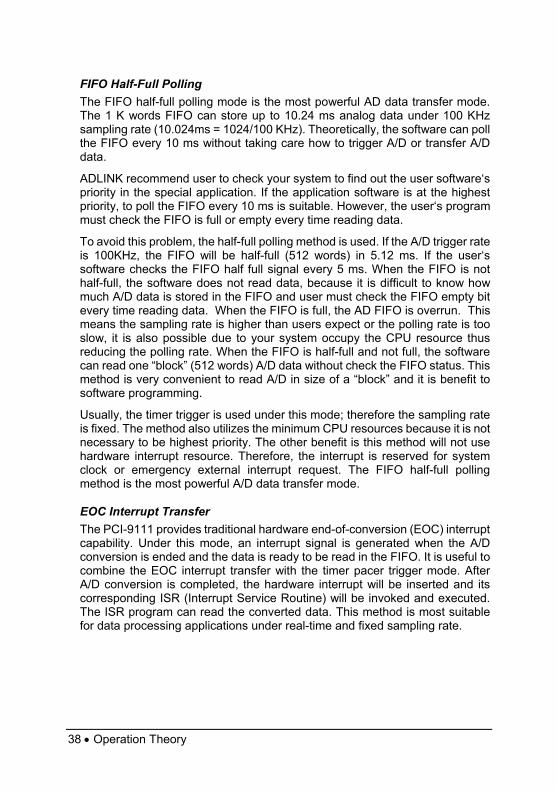
The Pre-Trigger timing is shown as following:
Figure 11. Pre-Trigger timing
If the application acquires data after the pre-trigger signal, only the last N data need to be stored. The maximum value of N is 65535. If the application only needs to acquire data before the pre-trigger signal, set N=1 then just one more data will be sampled after pre-trigger signal and infinite data before pre-trigger signal can be stored.
Acquire N A/D data after Pre-trigger Signal is Inserted Acquire Infinite A/D data before
Pre-Trigger Signal is Inserted
Counter # 0 counting from N down to 0
Set Pre-Trigger mode
External Pre-Trigger Signal is Inserted
A/D Data Acquisition Stop
Time

Operation Theory • 41
4.1.6 Post-Trigger Control Another useful trigger mode is the Post-Trigger. Under “Post-Trigger” mode, the post-trigger (POTRG) signal (from pin-12 of CN3) is used to “START” the A/D sampling.
After setting up the Post-Trigger mode, the A/D converter will not acquire data until the post-trigger signal is asserted. Users can poll the FIFO empty bit (FF_EF) to detect whether the Post-Trigger signal is asserted or not. Once the post-trigger is asserted, the hardware will begin to acquire data. Different from Pre-Trigger control mode, user can acquire data continuously until the Post-Trigger mode is disabled.
The following steps can be referenced for Post-Trigger control:
1. Disable all A/D trigger sources, ex: Timer-Pacer / Software trigger (TPST = 0) and External / Internal trigger (EITS = 0). Set Post-Trigger mode ON: POTRG = ON.
2. Set up A/D data acquire, including, A/D range, channel scan, data transfer mode and so on.
3. Reset FIFO.
4. Enable the selected A/D trigger source (Timer-Pacer, Software or external trigger).
5. Waiting for Post-Trigger signal assert. User can poll the FIFO empty bit to see if the post-trigger signal starts or not.
6. Once post-trigger signal asserts, user starts to process data. To stop data acquiring, disable the A/D trigger source.
7. Go to step 1 to start next Post-Trigger acquisition.
42 • Operation Theory
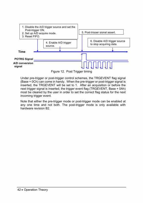
Figure 12. Post Trigger timing
Under pre-trigger or post-trigger control schemes, the TRGEVENT flag signal (Base + 0Ch) can come in handy. When the pre-trigger or post-trigger signal is inserted, the TRGEVENT will be set to 1. After an acquisition or before the next trigger signal is inserted, the trigger event flag (TRGEVENT, Base + 0Ah) most be cleared by the user in order to set the correct flag status for the next incoming trigger event.
Note that either the pre-trigger mode or post-trigger mode can be enabled at any one time and not both. The post-trigger mode is only available with hardware revision B2.
Time
POTRG Signal
1. Disable the A/D trigger source and set the Post-trigger ON.
2. Set up A/D acquire mode. 3. Reset FIFO.
4. Enable A/D trigger source.
5. Post-trigger signal assert.
6. Disable A/D trigger source to stop acquiring data.
A/D conversion signal
Operation Theory • 43
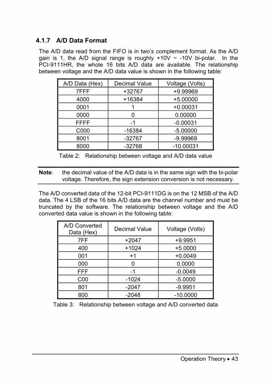
4.1.7 A/D Data Format The A/D data read from the FIFO is in two’s complement format. As the A/D gain is 1, the A/D signal range is roughly +10V ~ -10V bi-polar. In the PCI-9111HR, the whole 16 bits A/D data are available. The relationship between voltage and the A/D data value is shown in the following table:
A/D Data (Hex) Decimal Value Voltage (Volts) 7FFF +32767 +9.99969 4000 +16384 +5.00000 0001 1 +0.00031 0000 0 0.00000 FFFF -1 -0.00031 C000 -16384 -5.00000 8001 -32767 -9.99969 8000 -32768 -10.00031
Table 2: Relationship between voltage and A/D data value
Note: the decimal value of the A/D data is in the same sign with the bi-polar voltage. Therefore, the sign extension conversion is not necessary.
The A/D converted data of the 12-bit PCI-9111DG is on the 12 MSB of the A/D data. The 4 LSB of the 16 bits A/D data are the channel number and must be truncated by the software. The relationship between voltage and the A/D converted data value is shown in the following table:
A/D Converted Data (Hex) Decimal Value Voltage (Volts)
7FF +2047 +9.9951 400 +1024 +5.0000 001 +1 +0.0049 000 0 0.0000 FFF -1 -0.0049 C00 -1024 -5.0000 801 -2047 -9.9951 800 -2048 -10.0000
Table 3: Relationship between voltage and A/D converted data
44 • Operation Theory
The formula between the A/D converted data and the voltage value is:
Voltage AD dataK gain
= × ×_ 1 10
Where gain is the value of the A/D gain control register. K=32768 for PCI-9111HR, and K=2048 for PCI-9111DG.
4.2 Interrupt Control
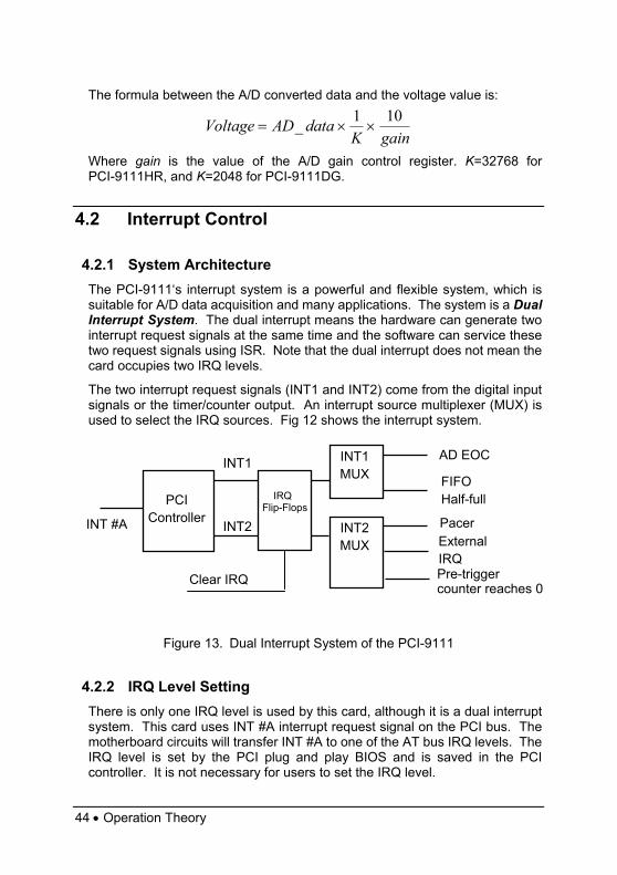
4.2.1 System Architecture The PCI-9111‘s interrupt system is a powerful and flexible system, which is suitable for A/D data acquisition and many applications. The system is a Dual Interrupt System. The dual interrupt means the hardware can generate two interrupt request signals at the same time and the software can service these two request signals using ISR. Note that the dual interrupt does not mean the card occupies two IRQ levels.
The two interrupt request signals (INT1 and INT2) come from the digital input signals or the timer/counter output. An interrupt source multiplexer (MUX) is used to select the IRQ sources. Fig 12 shows the interrupt system.
Figure 13. Dual Interrupt System of the PCI-9111
4.2.2 IRQ Level Setting There is only one IRQ level is used by this card, although it is a dual interrupt system. This card uses INT #A interrupt request signal on the PCI bus. The motherboard circuits will transfer INT #A to one of the AT bus IRQ levels. The IRQ level is set by the PCI plug and play BIOS and is saved in the PCI controller. It is not necessary for users to set the IRQ level.
PCI
Controller INT #A
IRQ Flip-Flops
INT1
Clear IRQ
INT2 MUX
Pacer INT2
INT1 MUX
AD EOC
FIFO Half-full
External IRQ Pre-trigger counter reaches 0
Operation Theory • 45
4.2.3 Dual Interrupt System The PCI controller of the PCI-9111 can receive two hardware IRQ sources. However, a PCI controller can generate only one IRQ on the PCI bus, the two IRQ sources must be distinguished by the ISR of the application software if the two IRQ are both used.
The application software can use the “_9111_Get_Irq_Status” function to distinguish which interrupt is inserted. After servicing an IRQ signal, users must check if another IRQ is also asserted, then clear the current IRQ to allow the next IRQ to occur.
The two IRQs are named as INT1 and INT2. INT1 comes from AD EOC or the FIFO half-full flag. INT2 comes from timer‘s pacer output or the external interrupt request or when the pre-trigger counter reaches to 0. The sources of INT1 and INT2 are selective by the Interrupt Control (ISC) Register.
Because the PCI-9111 is a dual interrupt system, you can use the FIFO half-full and external interrupt at the same time if your software ISR can distinguish these two events.
4.2.4 Interrupt Source Control There are three bits to control the IRQ sources of INT1 and INT2. Refer to section 3.10 for details of these bits. In addition, the PCI controller itself can also control the usage of the interrupt. To manipulate the interrupt system more easily, ADLINK recommends you use the function _9111_INT_Source_Control to control the IRQ source so that you can disable one or two of the IRQ sources.
Note that even if you disable both IRQ sources without changing the initial condition of the PCI controller, the PCI BIOS will still assign an IRQ level to the PCI card and will still occupy the PC’s resources. It is not recommended that the PCI cards initial condition be re-design with a users‘ application software. If users wish to disable the IRQ level, use the ADLINK software utility to change the interrupt settings.
46 • Operation Theory
4.3 Extended Digital I/O Port There are 4 extended digital input (EDI) signals and 4 extended digital output (EDO) signals on CN3 connector. The 4 EDI signals are dedicated used as input signal, however the 4 EDO signals can be used as digital input (Mode 1), digital output (Mode 2) or channel number output (Mode 3).
For power on safety, the EDO channel is set to be input when power on initial. To modify the configuration of the usage of the signals, please use the “_9111_Set_EDO_Function” in the library.
Note that when set the EDO function as channel number output (Mode 3), it presents the high nibble (4 MSBs) of the channel number no matter manual scan or auto scan mode.
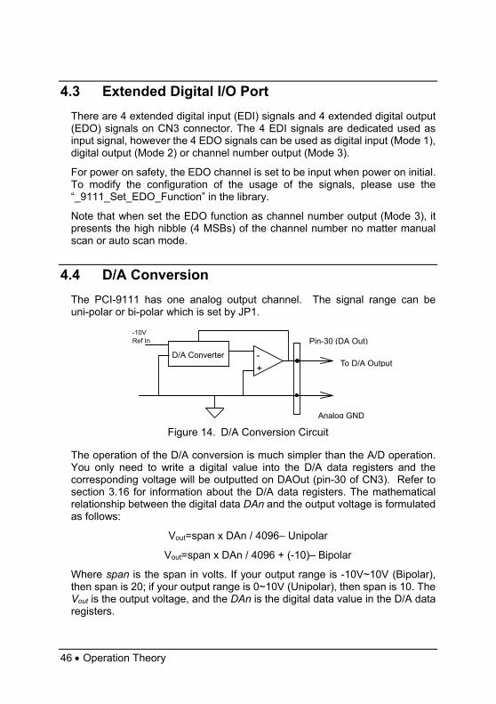
4.4 D/A Conversion The PCI-9111 has one analog output channel. The signal range can be uni-polar or bi-polar which is set by JP1.
To D/A OutputD/A Converter -
+
-10VRef In
Analog GND
Pin-30 (DA Out)
Figure 14. D/A Conversion Circuit
The operation of the D/A conversion is much simpler than the A/D operation. You only need to write a digital value into the D/A data registers and the corresponding voltage will be outputted on DAOut (pin-30 of CN3). Refer to section 3.16 for information about the D/A data registers. The mathematical relationship between the digital data DAn and the output voltage is formulated as follows:
Vout=span x DAn / 4096– Unipolar
Vout=span x DAn / 4096 + (-10)– Bipolar
Where span is the span in volts. If your output range is -10V~10V (Bipolar), then span is 20; if your output range is 0~10V (Unipolar), then span is 10. The Vout is the output voltage, and the DAn is the digital data value in the D/A data registers.

Operation Theory • 47
Before performing the D/A conversion, users should take note of the D/A output range, which is set by JP1. Refer to section 2.4 for jumper setting.
Analog Output Digital Data Input Unipolar
0V ~ 10V Bipolar
-10V ~ 10V FFF hex +9.9976V +9.9951V
800 hex +5.0000V 0.0000V
7FF hex +4.9976V -0.0049V
000 hex 0.0000V -10.0000V
1 LSB 2.44mV 4.88mV
Table 4: Relationship between DI and AO
4.5 Digital Input and Output To program the digital I/O operation is fairly straightforward. The digital input operation just reads data from its corresponding registers, and the digital output operation writes data to its corresponding registers. The digital I/O registers‘ format is shown in section 3.15. Note that the DIO data channel can only be read or written in the form of 16 bits. It is impossible to access individual bits.
The PCI-9111 provides 16 digital input and 16 digital output channels through CN1 and CN2. The digital I/O signals are fully TTL/DTL compatible. Detailed digital I/O signal specification can be referred to in section 1.3.
Digital Output (DO)
Digital GND (DGND)
Digital Input(DI) From TTL Signal
To TTL Devices
PCI-9111 Outside Device
74LS244
74LS373
Figure 15. Digital Input and Output circuit
48 • Operation Theory
4.6 Timer/Counter Operation 4.6.1 Introduction
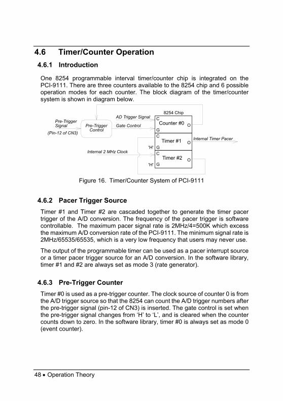
One 8254 programmable interval timer/counter chip is integrated on the PCI-9111. There are three counters available to the 8254 chip and 6 possible operation modes for each counter. The block diagram of the timer/counter system is shown in diagram below.
Counter #0
Internal 2 MHz Clock
Timer #1 Internal Timer Pacer
Timer #2
8254 Chip
G C
G C
G O
O
O
'H'
'H'
AD Trigger Signal
Gate ControlPre-TriggerControl
Pre-Trigger Signal
(Pin-12 of CN3)
C
Figure 16. Timer/Counter System of PCI-9111
4.6.2 Pacer Trigger Source Timer #1 and Timer #2 are cascaded together to generate the timer pacer trigger of the A/D conversion. The frequency of the pacer trigger is software controllable. The maximum pacer signal rate is 2MHz/4=500K which excess the maximum A/D conversion rate of the PCI-9111. The minimum signal rate is 2MHz/65535/65535, which is a very low frequency that users may never use.
The output of the programmable timer can be used as a pacer interrupt source or a timer pacer trigger source for an A/D conversion. In the software library, timer #1 and #2 are always set as mode 3 (rate generator).
4.6.3 Pre-Trigger Counter Timer #0 is used as a pre-trigger counter. The clock source of counter 0 is from the A/D trigger source so that the 8254 can count the A/D trigger numbers after the pre-trigger signal (pin-12 of CN3) is inserted. The gate control is set when the pre-trigger signal changes from ‘H’ to ‘L’, and is cleared when the counter counts down to zero. In the software library, timer #0 is always set as mode 0 (event counter).

Operation Theory • 49
4.6.4 I/O Address The 8254 in the PCI-9111 occupy 4 I/O address as shown below. BASE + 40 h LSB OR MSB OF COUNTER 0 BASE + 42 h LSB OR MSB OF COUNTER 1 BASE + 44 h LSB OR MSB OF COUNTER 2 BASE + 46 h CONTROL BYTE
The registers BASE+0 to BASE+3 control the programming of the 8254. Users can refer to the 82C54 data sheet for more details of the 82C54. You can download the data sheet at the following web site: “http://support.intel.com/support/controllers/peripheral/231164.htm” or “http://www.tundra.com/”
50 • C/C++ Library
5
C/C++ Library
This chapter describes the software library that operates the PCI-9111. Only the functions in DOS library and Windows 95 DLL are described. Refer to the PCIS-DASK function reference manual, which is included in ADLINK CD, for descriptions of Windows 98/NT/2000 DLL functions.
The function prototypes and useful constants are defined in the header files in the LIB (DOS) and INCLUDE (Windows 95) directories. For Windows 95 DLL, the developing environment can be Visual Basic 4.0 or above, Visual C/C++ 4.0 or above, Borland C++ 5.0 or above, Borland Delphi 2.x (32-bit) or above, or any Windows programming language that allows calls to a DLL.
5.1 Libraries Installation Please refer to the “Software Installation Guide” for information on how to install the software libraries for DOS, and Windows 95 DLL, or PCIS-DASK for Windows 98/NT/2000.
The device drivers and DLL functions for Windows 98/NT/2000 are included in the PCIS-DASK. Please refer to the PCIS-DASK user’s guide and function reference, which are included in the ADLINK CD, for detailed programming information.
C/C++ Library • 51
5.2 Programming Guide
5.2.1 Naming Convention The functions of the NuDAQ PCI or NuIPC CompactPCI card software drivers uses full-names to represent the functions' real meaning. The naming convention rules are:
In DOS Environment:
_hardware_model_action_name. e.g. _9111_Initial().
All functions in PCI-9111 driver are with 9111 as hardware_model. But they can be used by PCI-9111DG, PCI-9111HR.
In order to recognize the difference between a DOS library and a Windows 95 library, a capital "W" placed at the start of each function name for Windows 95 DLL drivers, e.g. W_9111_Initial().
5.2.2 Data Types We have defined some data type in Pci_9111.h (DOS) and Acl_pci.h (Windows 95). These data types are used by NuDAQ Cards’ library. We suggest you use these data types in your application programs. The following table shows the data type names and their range.
Type Name Description Range U8 8-bits ASCII character 0 to 255 I16 16-bits signed integer -32768 to 32767
U16 16-bits unsigned integer
0 to 65535
I32 32-bits signed integer -2147483648 to 2147483647
U32 32-bits unsigned integer
0 to 4294967295
F32 32-bits single-precision floating-point
-3.402823E38 to 3.402823E38
F64 64-bits double-precision floating-point
-1.797683134862315E308 to 1.797683134862315E309
Boolean Boolean logic value TRUE, FALSE
Table 5: Data types and corresponding range.
52 • C/C++ Library
5.3 _9111_Initial @ Description
This function is used to initialize the PCI_9111. Every PCI_9111 card must be initialized by this function before other function calls are permitted.
@ Syntax C/C++ (DOS) U16 _9111_Initial (U16 *existCards, PCI_INFO *info)
C/C++ (Windows 95) U16 W_9111_Initial (U16 *existCards, PCI_INFO *info)
Visual Basic (Windows 95) W_9111_Initial (existCards As Integer, info As PCI_INFO) As Integer
@ Argument existCards: number of existing PCI-9111 cards pciInfo: information about the PCI-9111 cards
@ Return Code ERR_NoError ERR_BoardNoInit ERR_PCIBiosNotExist
5.4 _9111_DO @ Description
This function is used to write data to the digital output port. There are 16 digital output channels on the PCI_9111.
@ Syntax C/C++ (DOS) U16 _9111_DO (U16 cardNo, U16 DOData)
C/C++ (Windows 95) U16 W_9111_DO (U16 cardNo, U16 DOData)
Visual Basic (Windows 95) W_9111_DO (ByVal cardNo As Integer, ByVal DOData As Integer) As Integer
@ Argument cardNo: The card number of the PCI-9111 card initialized DOData: The value written to the digital output port
@ Return Code ERR_NoError
C/C++ Library • 53
5.5 _9111_DO_Channel @ Description
This function is used to write data to the digital output ports. There are 16 digital output channels on the PCI_9111. You can control each digital output channel using this function. When performing this function, the digital output port is written to and the output status is changed to the value you had specified by do_data.
@ Syntax C/C++ (DOS) U16 _9111_DO_Channel (U16 cardNo, U16 do_ch_no , Boolean do_data)
C/C++ (Windows 95) U16 W_9111_DO_Channel (U16 cardNo, U16 do_ch_no , Boolean do_data)
Visual Basic (Windows 95) W_9111_DO_ByVal cardNo As Integer, ByVal do_ch_no As Integer, ByVal do_data As Byte) As Integer
@ Argument cardNo: The card number of PCI-9111 card initialized do_ch_no: The channel number to perform the digital output, the value
is between 0 to 15. do_data: The value written to digital output port, either 0 or 1.
@ Return Code ERR_NoError ERR_InvalidDOChannel
54 • C/C++ Library
5.6 _9111_DI @ Description
This function is used to read data from the digital input ports. There are 16 digital input channels on the PCI_9111. The digital input status can be accessed using this function.
@ Syntax C/C++ (DOS) U16 _9111_DI (U16 cardNo, U16 *DIData)
C/C++ (Windows 95) U16 W_9111_DI (U16 cardNo, U16 *DIData)
Visual Basic (Windows 95) W_9111_DI (ByVal cardNo As Integer, DIData As Integer) As Integer
@ Argument cardNo: The card number of PCI-9111 card initialized DIData: The value accessed from the digital input port
@ Return Code ERR_NoError
C/C++ Library • 55
5.7 _9111_DI_Channel @ Description
This function is used to read data from the digital input port. There are 16 digital input channels on the PCI_9111. You can read each digital input channel using this function. While performing this function, the digital input port is read and the value of the specified channel is stored in *data.
@ Syntax C/C++ (DOS) U16 _9111_DI_Channel (U16 cardNo, U16 di_ch_no , Boolean *di_data )
C/C++ (Windows 95) U16 W_9111_DI_Channel (U16 cardNo, U16 di_ch_no , Boolean *di_data )
Visual Basic (Windows 95) W_DAQ1210_DI_Channel (ByVal cardNo As Integer, ByVal di_ch_no As Integer, di_data As Byte) As Integer
@ Argument cardNo: The card number of PCI-9111 card initialized di_ch_no: The channel number to perform the digital output, the value
is between 0 to 15. di_data: The value read from the digital input channel, either 0 or 1.
@ Return Code ERR_NoError ERR_InvalidDIChannel
56 • C/C++ Library
5.8 _9111_EDI @ Description
There are 4 extended digital input channels on the PCI_9111. This function is used to read data from the extended digital input ports. The retrieved data is stored in DIData and only the 4 LSB of the DIData are valid input data.
@ Syntax C/C++ (DOS) U16 _9111_EDI (U16 cardNo, U16 *DIData)
C/C++ (Windows 95) U16 W_9111_EDI (U16 cardNo, U16 *DIData)
Visual Basic (Windows 95) W_9111_EDI (ByVal cardNo As Integer, DIData As Integer) As Integer
@ Argument cardNo: The card number of PCI-9111 card initialized DIData: The value accessed from the extended digital input port
@ Return Code ERR_NoError
C/C++ Library • 57
5.9 _9111_EDO @ Description
There are 4 extended digital output channels on the PCI_9111. This function is used to write data to the extended digital output port. The extended digital output channels can be set with 3 different modes (refer to chapter 4); however, the output EDO value can only be place on the EDO pins when the EDO mode is set as EDO_OUT_CHN. Therefore, the program must call the _9111_Set_EDO_Function function (refer to chapter 4) to set the EDO mode as EDO_OUT_EDO before writing data to the EDO channels.
@ Syntax C/C++ (DOS) U16 _9111_EDO (U16 cardNo, U16 DOData)
C/C++ (Windows 95) U16 W_9111_EDO (U16 cardNo, U16 DOData)
Visual Basic (Windows 95) W_9111_EDO (ByVal cardNo As Integer, ByVal DOData As Integer) As Integer
@ Argument cardNo: The card number of PCI-9111 card initialized DOData: The value written to the extended digital input port
@ Return Code ERR_NoError
58 • C/C++ Library
5.10 _9111_EDO_Read_Back @ Description
This function is used to read back the output data that is written to the output port previously.
@ Syntax C/C++ (DOS) U16 _9111_EDO_Read_Back (U16 cardNo, U16 *DOData )
C/C++ (Windows 95) U16 W_9111_EDO_Read_Back (U16 cardNo, U16 *DOData )
Visual Basic (Windows 95) W_9111_EDO_Read_Back (ByVal cardNo As Integer, DOData As Integer) As Integer
@ Argument cardNo: The card number of PCI-9111 card initialized DOData: The read back value
@ Return Code ERR_NoError
5.11 _9111_Set_EDO_Function @ Description
The 4 EDO channels on the PCI-9111 can be used as a digital output (EDO_OUT_EDO), digital input (EDO_INPUT) or channel number output (EDO_OUT_CHN). This function is used to set the mode of the EDO pins.
@ Syntax C/C++ (DOS) U16 _9111_Set_EDO_Function (U16 cardNo, U16 x)
C/C++ (Windows 95) U16 W_9111_Set_EDO_Function (U16 cardNo, U16 x )
Visual Basic (Windows 95) W_9111_Set_EDO_Function (ByVal cardNo As Integer, ByVal x As Integer) As Integer
@ Argument cardNo: The card number of PCI-9111 card initialized x: The mode of the EDO pins, valid modes are: EDO_INPUT, EDO_OUT_EDO, EDO_OUT_CHN
@ Return Code ERR_NoError
C/C++ Library • 59
5.12 _9111_DA @ Description
This function is used to write data to the D/A converters. There is one Digital-to-Analog conversion channel on the PCI-9111. The resolution of each channel is 12-bit; i.e. the range is from 0 to 4095.
@ Syntax C/C++ (DOS) U16 _9111_DA (U16 cardNo, I16 DAData)
C/C++ (Windows 95) U16 W_9111_DA (U16 cardNo, I16 DAData )
Visual Basic (Windows 95) W_9111_DA (ByVal cardNo As Integer, ByVal DAData As Integer) As Integer
@ Argument cardNo: The card number of PCI-9111 card initialized DAData: D/A converted value, refer to chapter 4 for the relationship
between the voltage and digital value @ Return Code
ERR_NoError
5.13 _9111_AD_Read_Data @ Description
This function is used to read the AD converted data from the analog input port.
@ Syntax C/C++ (DOS) U16 _9111_AD_Read_Data (U16 cardNo, I16 far *ADData)
C/C++ (Windows 95) U16 W_9111_AD_Read_Data (U16 cardNo, I16 *ADData)
Visual Basic (Windows 95) W_9111_AD_Read_Data (ByVal cardNo As Integer, ADData As Integer) As Integer
@ Argument cardNo: The card number of PCI-9111 card initialized ADData: A/D converted value, Refer to chapter 4 for relationship
between the voltage and digital value @ Return Code
ERR_NoError
60 • C/C++ Library
5.14 _9111_AD_Read_Data_Repeat @ Description
This function is used to read the AD converted data n times continuously.
@ Syntax C/C++ (DOS) U16 _9111_AD_Read_Data_Repeat (U16 cardNo, I16 far *ADData, U16 n)
C/C++ (Windows 95) U16 W_9111_AD_Read_Data_Repeat (U16 cardNo, I16 *ADData, U16 n)
Visual Basic (Windows 95) W_9111_AD_Read_Data_Repeat (ByVal cardNo As Integer, ADData As Integer, ByVal n As Integer) As Integer
@ Argument cardNo: The card number of PCI-9111 card initialized ADData: A/D converted value, Refer to chapter 4 for relationship
between the voltage and digital value n: The number of times to read the AD converted data
@ Return Code ERR_NoError
C/C++ Library • 61
5.15 _9111_AD_Set_Channel @ Description
This function is used to set the AD channel by means of writing data to the multiplexer scan channel register. There are 16 single-ended A/D channels on the PCI-9111; therefore the channel number can be set between 0 and 15. Under non-auto scan mode, the ADChannelNo stores the channel number setting. Under auto-scan mode, the ADChannelNo records the ending channel number.
@ Syntax C/C++ (DOS) U16 _9111_AD_Set_Channel (U16 cardNo, U16 ADChannelNo)
C/C++ (Windows 95) U16 W_9111_AD_Set_Channel (U16 cardNo, U16 ADChannelNo)
Visual Basic (Windows 95) W_9111_AD_Set_Channel (ByVal cardNo As Integer, ByVal ADChannelNo As Integer) As Integer
@ Argument cardNo: The card number of PCI-9111 card initialized. ADChannelNo:Selected channel number or the ending channel number
to perform the A/D conversion. @ Return Code
ERR_NoError
62 • C/C++ Library
5.16 _9111_AD_Get_Channel @ Description
This function reads from the multiplexer scan channel register and obtains the AD channel number and the stores the value in ADChannelNo. Under non-auto scan mode, bits 0 to 3 of the ADChannelNo stores the channel number setting and bits 4 to 7 of the ADChannel are all ‘0”. Under auto-scan mode, bits 0 to 3 of the ADChannelNo record the ending channel number. Bits 4 to 7 of ADChannelNo are the selected channel.
@ Syntax C/C++ (DOS) U16 _9111_AD_Get_Channel (U16 cardNo, U16 *ADChannelNo )
C/C++ (Windows 95) U16 W_9111_AD_Get_Channel (U16 cardNo, U16 *ADChannelNo)
Visual Basic (Windows 95) W_9111_AD_Get_Channel (ByVal cardNo As Integer, ADChannelNo As Integer) As Integer
@ Argument cardNo: The card number of PCI-9111 card initialized ADChannelNo: Channel number to perform the A/D conversion
@ Return Code ERR_NoError
C/C++ Library • 63
5.17 _9111_AD_Set_Range @ Description
This function is used to set the A/D range by means of writing data to the gain control register. The initial value of gain is '1' which is the default setting by the PCI-9111 hardware. The relationship between gain and input voltage ranges in the following table:
Input Range (V) Gain Gain Code ±10 V X 1 AD_B_10_V ±5 V X 2 AD_B_5_V ±2.5 V X 4 AD_B_2_5_V ±1.25 V X 8 AD_B_1_25_V ±0.625V X 16 AD_B_0_625_V
@ Syntax C/C++ (DOS) U16 _9111_AD_Set_Range (U16 cardNo, U16 ADRange)
C/C++ (Windows 95) U16 W_9111_AD_Set_Range (U16 cardNo, U16 ADRange)
Visual Basic (Windows 95) W_9111_AD_Set_Range (ByVal cardNo As Integer, ByVal ADRange As Integer) As Integer
@ Argument cardNo: The card number of PCI-9111 card initialized ADRange: The programmable gain of A/D conversion, the possible
values are: AD_B_10_V, AD_B_5_V, AD_B_2_5_V, AD_B_1_25_V, AD_B_0_625_V.
@ Return Code ERR_NoError
64 • C/C++ Library
5.18 _9111_AD_Get_Range @ Description
This function is used to get the A/D range from the gain control register. The relationship between the gains and input voltage ranges are specified in the table below.
Input Range (V) Gain Gain Code ±10 V X 1 AD_B_10_V ±5 V X 2 AD_B_5_V ±2.5 V X 4 AD_B_2_5_V ±1.25 V X 8 AD_B_1_25_V ±0.625V X 16 AD_B_0_625_V
@ Syntax C/C++ (DOS) U16 _9111_AD_Get_Range (U16 cardNo, U16 *ADRange)
C/C++ (Windows 95) U16 W_9111_AD_Get_Range (U16 cardNo, U16 *ADRange)
Visual Basic (Windows 95) W_9111_AD_Get_Range (ByVal cardNo As Integer, ADRange As Integer) As Integer
@ Argument cardNo: The card number of PCI-9111 card initialized ADRange: The programmable gain of A/D conversion, the possible
values are: AD_B_10_V, AD_B_5_V, AD_B_2_5_V, AD_B_1_25_V, AD_B_0_625_V.
@ Return Code ERR_NoError
C/C++ Library • 65
5.19 _9111_AD_Get_Status @ Description
This function is used to get AD FIFO status from the gain control register.
@ Syntax C/C++ (DOS) U16 _9111_AD_Get_Status (U16 cardNo, U16 *ADStatus)
C/C++ (Windows 95) U16 W_9111_AD_Get_Status (U16 cardNo, U16 *ADStatus)
Visual Basic (Windows 95) W_9111_AD_Get_Status (ByVal cardNo As Integer, ADStatus As Integer) As Integer
@ Argument cardNo: The card number of PCI-9111 card initialized ADStatus: The status of AD FIFO. The AD FIFO status could be one of
the following: ADSTS_FF_EF:FIFO is empty ADSTS_FF_HF:FIFO is half-full ADSTS_FF_FF:FIFO is full, A/D data may have been loss ADSTS_BUSY:AD is busy, A/D data is written into FIFO.
@ Return Code ERR_NoError
66 • C/C++ Library
5.20 _9111_AD_Set_Mode @ Description
This function is used to set AD trigger and channel scan mode. Please refer to section 5.1.3 for the detailed description of AD trigger modes and section 5.1.5 for the description of Pre-Trigger mode control.
@ Syntax C/C++ (DOS) U16 _9111_AD_Set_Mode (U16 cardNo, U16 ADMode)
C/C++ (Windows 95) U16 W_9111_AD_Set_Mode (U16 cardNo, U16 ADMode)
Visual Basic (Windows 95) W_9111_AD_Set_Mode (ByVal cardNo As Integer, ByVal ADMode As Integer) As Integer
@ Argument cardNo: The card number of PCI-9111 card initialized ADMode: The value of AD mode. The mode could be one or a
combination of the following modes: A_9111_AD_Clear_TRGEVENT A_9111_AD_PostTrg_ON A_9111_AD_PostTrg_OFF A_9111_AD_PreTrg_ON A_9111_AD_PreTrg_OFF A_9111_AD_External_SRC A_9111_AD_Internal_SRC A_9111_AD_TimerTrig A_9111_AD_SoftTrig A_9111_AD_AutoScan
@ Return Code ERR_NoError
C/C++ Library • 67
5.21 _9111_AD_Get_Mode @ Description
This function is used to get AD mode. Please refer to section 5.1.3 for the detailed description of AD trigger modes and section 5.1.5 for the description of Pre-Trigger mode control.
@ Syntax C/C++ (DOS) U16 _9111_AD_Get_Mode (U16 cardNo, U16 *ADMode)
C/C++ (Windows 95) U16 W_9111_AD_Get_Mode (U16 cardNo, U16 *ADMode)
Visual Basic (Windows 95) W_9111_AD_Get_Mode (ByVal cardNo As Integer, ADMode As Integer) As Integer
@ Argument cardNo: The card number of PCI-9111 card initialized ADMode: The value of AD mode. The returned value could be one or a
combination of the following modes: A_9111_AD_PostTrg_ON A_9111_AD_PostTrg_OFF A_9111_AD_PreTrg_ON A_9111_AD_PreTrg_OFF A_9111_AD_External_SRC A_9111_AD_Internal_SRC A_9111_AD_TimerTrig A_9111_AD_SoftTrig A_9111_AD_AutoScan
@ Return Code ERR_NoError
68 • C/C++ Library
5.22 _9111_INT_Set_Reg @ Description
This function is used to select the interrupt sources by writing data to interrupt control register. Refer to section 3.10 for details of how to setup the interrupt control register.
@ Syntax C/C++ (DOS) U16 _9111_INT_Set_Reg (U16 cardNo, U16 INTC)
C/C++ (Windows 95) U16 W_9111_INT_Set_Reg (U16 cardNo, U16 INTC)
Visual Basic (Windows 95) W_9111_INT_Set_Reg (ByVal cardNo As Integer, ByVal INTC As Integer) As Integer
@ Argument cardNo: The card number of PCI-9111 card initialized INTC: The value written to the interrupt control register, refer to
section 3.10 for ISC0, ISC1 and ISC2 settings. Note that the ISC2 control bit is only supported with hardware revision B2.
@ Return Code ERR_NoError ERR_BoardNoInit
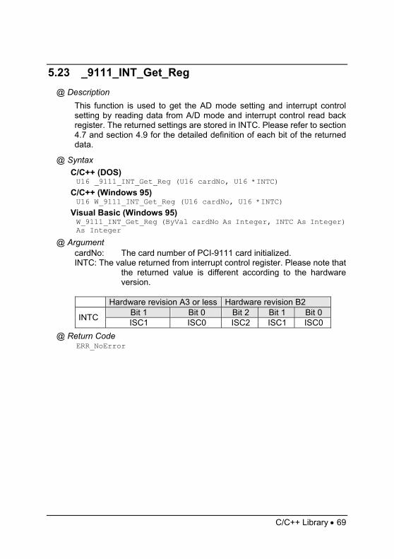
C/C++ Library • 69
5.23 _9111_INT_Get_Reg @ Description
This function is used to get the AD mode setting and interrupt control setting by reading data from A/D mode and interrupt control read back register. The returned settings are stored in INTC. Please refer to section 4.7 and section 4.9 for the detailed definition of each bit of the returned data.
@ Syntax C/C++ (DOS) U16 _9111_INT_Get_Reg (U16 cardNo, U16 *INTC)
C/C++ (Windows 95) U16 W_9111_INT_Get_Reg (U16 cardNo, U16 *INTC)
Visual Basic (Windows 95) W_9111_INT_Get_Reg (ByVal cardNo As Integer, INTC As Integer) As Integer
@ Argument cardNo: The card number of PCI-9111 card initialized. INTC: The value returned from interrupt control register. Please note that
the returned value is different according to the hardware version.
Hardware revision A3 or less Hardware revision B2
Bit 1 Bit 0 Bit 2 Bit 1 Bit 0 INTC ISC1 ISC0 ISC2 ISC1 ISC0 @ Return Code
ERR_NoError
70 • C/C++ Library
5.24 _9111_Reset_FIFO @ Description
The PCI-9111 A/D data are stored in the FIFO after conversion. This function is used to reset A/D FIFO. This function should be called before performing A/D conversion to clear the old data stored in the FIFO.
@ Syntax C/C++ (DOS) U16 _9111_Reset_FIFO (U16 cardNo)
C/C++ (Windows 95) U16 W_9111_Reset_FIFO (U16 cardNo)
Visual Basic (Windows 95) W_9111_Reset_FIFO (ByVal cardNo As Integer) As Integer
@ Argument cardNo: The card number of PCI-9111 card initialized.
@ Return Code ERR_NoError ERR_BoardNoInit
C/C++ Library • 71
5.25 _9111_AD_Soft_Trigger @ Description
This function is used to trigger the A/D conversion by software. When the function is called, a trigger pulse will be generated and the converted data will be stored from address Base +0.
@ Syntax C/C++ (DOS) U16 _9111_AD_Soft_Trigger (U16 cardNo)
C/C++ (Windows 95) U16 W_9111_AD_Soft_Trigger (U16 cardNo)
Visual Basic (Windows 95) W_9111_AD_Soft_Trigger (ByVal cardNo As Integer) As Integer
@ Argument cardNo: The card number of PCI-9111 card initialized.
@ Return Code ERR_NoError
5.26 _9111_Set_8254 @ Description
This function is used to write PCI-9111 8254 Programmable Timer.
@ Syntax C/C++ (DOS) U16 _9111_Set_8254 (U16 cardNo, U16 ChannelNo, U8 count)
C/C++ (Windows 95) U16 W_9111_Set_8254 (U16 cardNo, U16 ChannelNo, U8 count)
Visual Basic (Windows 95) W_9111_Set_8254 (ByVal cardNo As Integer, ByVal ChannelNo As Integer, ByVal count As Byte) As Integer
@ Argument cardNo: The card number of PCI-9111 card initialized. Tmr_ch: Port of 8254 Timer, the value is within 0 to 3. count: value to write, only 8 LSBs are effective
@ Return Code ERR_NoError
72 • C/C++ Library
5.27 _9111_Get_8254 @ Description
This function is used to read PCI-9111 8254 Programmable Timer. The read value are stored in count.
@ Syntax C/C++ (DOS) U16 _9111_Get_8254 (U16 cardNo, U16 ChannelNo, U8 *count)
C/C++ (Windows 95) U16 W_9111_Get_8254 (U16 cardNo, U16 ChannelNo, U8 *count)
Visual Basic (Windows 95) W_9111_Get_8254 (ByVal cardNo As Integer, ByVal ChannelNo As Integer, count As Byte) As Integer
@ Argument cardNo: The card number of PCI-9111 card initialized. Tmr_ch: Port of 8254 Timer, the value is within 0 to 3. count: value read from 8254 programmable timer, only 8 LSBs are
effective @ Return Code
ERR_NoError
C/C++ Library • 73
5.28 _9111_AD_Timer @ Description
This function is used to set the Timer #1 and Timer#2. Timer#1 and Timer#2 are used as frequency dividers for generating constant A/D sampling rate dedicatedly. It is possible to stop the pacer trigger by setting any one of the dividers as 0. Because the AD conversion rate is limited due to the conversion time of the AD converter, the highest sampling rate of the PCI-9111 can not be exceeded 110 KHz. The multiplication of the dividers must be larger than 20.
@ Syntax C/C++ (DOS) U16 _9111_AD_Timer (U16 cardNo, U16 c1, U16 c2)
C/C++ (Windows 95) U16 W_9111_AD_Timer (U16 cardNo, U16 c1, U16 c2)
Visual Basic (Windows 95) W_9111_AD_Timer (ByVal cardNo As Integer, ByVal c1 As Integer, ByVal c2 As Integer) As Integer
@ Argument cardNo: The card number of PCI-9111 card initialized. c1: frequency divider of timer #1 c2: frequency divider of timer #2
@ Return Code ERR_NoError

74 • C/C++ Library
5.29 _9111_Counter_Start @ Description
The counter #0 of the PCI-9111 Timer/Counter chip can be freely programmed by the users. This function is used to program the counter #0. This counter is used as the pre-trigger counter.
@ Syntax C/C++ (DOS) U16 _9111_Counter_Start (U16 cardNo, U16 mode, U16 c0)
C/C++ (Windows 95) U16 W_9111_Counter_Start (U16 cardNo, U16 mode, U16 c0)
Visual Basic (Windows 95) W_9111_Counter_Start (ByVal cardNo As Integer, ByVal mode As Integer, ByVal c0 As Integer) As Integer
@ Argument cardNo: The card number of PCI-9111 card initialized. Mode: the 8254 timer mode, the possible values are: TIMER_MODE0, TIMER_MODE1, TIMER_MODE2, TIMER_MODE3, TIMER_MODE4, TIMER_MODE5. Please refer to Counter/Timer 8254's reference manual for more detailed information of timer mode. c0: count value of counter#0
@ Return Code ERR_NoError
C/C++ Library • 75
5.30 _9111_Counter_Read @ Description
This function is used to read the count value of the Counter#0.
@ Syntax C/C++ (DOS) U16 _9111_Counter_Read (U16 cardNo, U16 *c0)
C/C++ (Windows 95) U16 W_9111_Counter_Read (U16 cardNo, U16 *c0)
Visual Basic (Windows 95) W_9111_Counter_Read (ByVal cardNo As Integer, c0 As Integer) As Integer
@ Argument cardNo: The card number of PCI-9111 card initialized. c0: count value of counter#0
@ Return Code ERR_NoError
5.31 _9111_Counter_Stop @ Description
This function is used to stop the timer operation. The timer is set as the “One-shot” mode with count value ‘0’. That is, the clock output signal will be set to high after executing this function.
@ Syntax C/C++ (DOS) U16 _9111_Counter_Stop (U16 cardNo, U16 *c0)
C/C++ (Windows 95) U16 W_9111_Counter_Stop (U16 cardNo, U16 *c0)
Visual Basic (Windows 95) U16 W_9111_Counter_Stop (ByVal cardNo As Integer, c0 As Integer) As Integer
@ Argument cardNo: The card number of PCI-9111 card initialized. c0: the current count value of the Counter#0
@ Return Code ERR_NoError
76 • C/C++ Library
5.32 _9111_INT_Source_Control @ Description
The PCI-9111 has a dual interrupt system, two interrupt sources can be generated and be checked by the software. This function is used to select and control the PCI-9111’s interrupt sources by writing data to the interrupt control register. Refer to section 5.2 for details of the interrupt system.
@ Syntax C/C++ (DOS) void _9111_INT_Source_Control (U16 cardNo, U16 int1Ctrl, U16 int2Ctrl)
C/C++ (Windows 95) void W_9111_INT_Source_Control (U16 cardNo, U16 int1Ctrl, U16 int2Ctrl)
Visual Basic (Windows 95) W_9111_INT_Source_Control (ByVal cardNo As Integer, ByVal int1Ctrl As Integer, ByVal int2Ctrl As Integer)
@ Argument cardNo: the card number of PCI-9111 card initialized. int1Ctrl: Values to control INT1, possible values are defined below: 0:INT1 disable 1:INT1 AD end of conversion (EOC) interrupt 2:INT1 FIFO half full int2Ctrl: Values to control INT2, possible values are defined below:
0:INT2 disable 1:INT2 pacer timer interrupt 2:INT2 external interrupt source 3:INT2 pre-trigger counter reaches to 0 (Only supported with
hardware version B2, refer to section 3.10 for details) @ Return Code
None
C/C++ Library • 77
5.33 _9111_CLR_IRQ @ Description
This function is used to clear interrupt request which is requested by PCI-9111. If you use EOC interrupt or FIFO half full interrupt to transfer A/D converted data, you should use this function to clear interrupt request status; otherwise, the new coming interrupt will not be generated.
@ Syntax C/C++ (DOS) void _9111_CLR_IRQ (U16 cardNo)
C/C++ (Windows 95) void W_9111_CLR_IRQ (U16 cardNo) Visual Basic(Windows 95) W_9111_CLR_IRQ (ByVal cardNo As Integer)
@ Argument None
@ Return Code None
5.34 _9111_Get_IRQ_Channel @ Description
This function is used to get the IRQ level of the PCI-9111 card used currently.
@ Syntax C/C++ (DOS) void _9111_Get_IRQ_Channel (U16 cardNo, U16 *irq_no)
C/C++ (Windows 95) void W_9111_Get_IRQ_Channel (U16 cardNo, U16 *irq_no)
Visual Basic (Windows 95) W_9111_Get_IRQ_Channel (ByVal cardNo As Integer, irq_no As Integer)
@ Argument cardNo: the card number of PCI-9111 card initialized. Irq_no: the IRQ level used to transfer A/D data for this card
@ Return Code None
78 • C/C++ Library
5.35 _9111_Get_IRQ_Status @ Description
This function is used to get the status of the two IRQs (INT1 and INT2) in PCI-9111 card.
@ Syntax C/C++ (DOS) void _9111_Get_IRQ_Status (U16 cardNo, U16 *ch1, U16 *ch2)
C/C++ (Windows 95) void W_9111_Get_IRQ_Status (U16 cardNo, U16 *ch1, U16 *ch2)
Visual Basic (Windows 95) W_9111_Get_IRQ_Status (ByVal cardNo As Integer, ch1 As Integer, ch2 As Integer)
@ Argument cardNo: the card number of PCI-9111 card initialized. ch1: the IRQ status of INT1, 0: no IRQ, 1: IRQ ch2: the IRQ status of INT2, 0: no IRQ, 1: IRQ
@ Return Code None
C/C++ Library • 79
5.36 _9111_AD_FFHF_Polling @ Description
This function is used to perform powerful AD data transfer by applying half-full polling mode. This method checks the FIFO half full signal every time call this function. If the FIFO is not half-full, the software do not read data. When the FIFO is full, the AD FIFO is overrun. When the FIFO is half-full but not full, software reads the A/D data, stored in FIFO, in size of one “block” (512 words). The FIFO half-full polling method is the most powerful A/D data transfer mode. Please refer to section 5.1.4 for the detailed description of half-full polling mode.
@ Syntax C/C++ (DOS) U16 _9111_AD_FFHF_Polling (U16 cardNo, I16 far *ad_data)
C/C++ (Windows 95) U16 W_9111_AD_FFHF_Polling (U16 cardNo, I16 *ad_data)
Visual Basic (Windows 95) W_9111_AD_FFHF_Polling (ByVal cardNo As Integer, ad_data As Integer) As Integer
@ Argument cardNo: the card number of PCI-9111 card initialized. ad_data: the 16bits A/D converted value. The data format can be
referred to section 5.1.6 for details. @ Return Code
ERR_NoError ERR_FIFO_Half_NotReady
80 • C/C++ Library
5.37 _9111_AD_Aquire @ Description
This function is used to trigger the A/D conversion data for PCI-9111 by software trigger. It reads the 12 bits A/D data when the data is ready.
@ Syntax C/C++ (DOS) U16 _9111_AD_Aquire (U16 cardNo, I16 far *ad_data)
C/C++ (Windows 95) U16 W_9111_AD_Aquire (U16 cardNo, I16 *ad_data)
Visual Basic (Windows 95) W_9111_AD_Aquire (ByVal cardNo As Integer, ad_data As Integer) As Integer
@ Argument cardNo: the card number of PCI-9111 card initialized. ad_data: the 12bits A/D converted value. The data format can be
referred to section 5.1.6 for details. @ Return Code
ERR_NoError ERR_AD_AquireTimeOut
C/C++ Library • 81
5.38 _9111_AD_HR_Aquire @ Description
This function is used to trigger the A/D conversion data for PCI-9111HR by software trigger. It reads the 16 bits A/D data when the data is ready.
@ Syntax C/C++ (DOS) U16 _9111_AD_HR_Aquire (U16 cardNo, I16 far *ad_data)
C/C++ (Windows 95) U16 W_9111_AD_HR_Aquire (U16 cardNo, I16 *ad_data)
Visual Basic (Windows 95) W_9111_AD_HR_Aquire (ByVal cardNo As Integer, ad_data As Integer) As Integer
@ Argument cardNo: the card number of PCI-9111 card initialized. ad_data: the 16bits A/D converted value. The data format can be
referred to section 5.1.6 for details. @ Return Code
ERR_NoError ERR_AD_AquireTimeOut
82 • C/C++ Library
5.39 _9111_AD_INT_Start @ Description
This function is used to initialize and start up the AD EOC (end-of-conversion) interrupt transfer mode. This function could perform A/D conversion N times with interrupt data transfer by using pacer trigger. It takes place in the background which will not stop until the N-th conversion has been completed or your program execute _9111_AD_INT_Stop() function to stop the process.
After executing this function, it is necessary to check the status of the operation by using the function _9111_AD_INT_Status(). While all the specified count of data are acquired, the interrupt status will be changed to “AD_INT_STOP”.The function can perform on single A/D channel (autoscan is disable) or multiple A/D channels (autoscan is enable) with fixed analog input range.
Note: The interrupt mode provided in this function is internal timer source; therefore you must specify c1 & c2 as calling this function. In addition, this function in this library supports just one PCI-9111 card and provides only one ISR (interrupt service routine) for processing the interrupt events. If multi-9111 cards and multi-ISR is necessary, users can modify this library for your own purpose.
@ Syntax C/C++ (DOS) U16 _9111_AD_INT_Start (U16 cardNo, U16 auto_scan, U16 ad_ch_no, U16 ad_gain, U16 count, I16 far *ad_buffer, U16 c1, U16 c2)
C/C++ (Windows 95) U16 W_9111_AD_INT_Start (U16 cardNo, U16 auto_scan, U16 ad_ch_no, U16 ad_gain, U16 count, I16 far *ad_buffer, U16 c1, U16 c2)
Visual Basic (Windows 95) W_9111_AD_INT_Start (ByVal cardNo As Integer, ByVal auto_scan As Integer, ByVal ad_ch_no As Integer, ByVal ad_gain As Integer, ByVal count As Integer, ad_buffer As Integer, ByVal c1 As Integer, ByVal c2 As Integer) As Integer
@ Argument cardNo: the card number of PCI-9111 card initialized. auto_scan: 0: autoscan is disabled. 1: autoscan is enabled. ad_ch_no: A/D channel number.
C/C++ Library • 83
If the auto_scan is set as enable, the selection sequence of A/D channel is: 0, 1, 2, 3, ... , [ad_ch_no], 0, 1, 2, 3, ... , [ad_ch_no], ... .
If the auto_scan is set as disable, only the data input from [ad_ch_no] is converted.
ad_gain: A/D analog input range, the possible values are: AD_B_10_V, AD_B_5_V, AD_B_2_5_V, AD_B_1_25_V,
AD_B_0_625_V, count: the number of A/D convertion ad_buffer: the start address of the memory buffer t store the AD data,
the buffer size must large than the number of AD conversion. c1: the frequency devider of Timer#1. c2: the frequency devider of Timer#2.
@ Return Code ERR_InvalidADChannel ERR_AD_InvalidGain ERR_InvalidTimerValue ERR_NoError
5.40 _9111_AD_FFHF_INT_Start @ Description
This function is used to initialize and start up AD FIFO Half Full Interrupt Transfer mode. This function could perform A/D conversion N times by using pacer trigger and perform data transfer by using AD FIFO Half Full Interrupt Transfer. It takes place in the background and will not stop until the N blocks of conversion has been completed or your program execute _9111_AD_INT_Stop() function to stop the process. After executing this function, it is necessary to check the status of the operation by using the function _9111_AD_FFHF_INT_Status(). While all the specified blocks of data are acquired, the interrupt status will be changed to “AD_FFHF_BLOCK_FULL”. The function can perform on single A/D channel (autoscan is disable) or multiple A/D channels (autoscan is enable) with fixed analog input range.
@ Syntax C/C++ (DOS) U16 _9111_AD_FFHF_INT_Start (U16 cardNo, U16 auto_scan, U16 ad_ch_no, U16 ad_gain, U16 blockNo, I16 far *ad_buffer, U16 c1, U16 c2)
C/C++ (Windows 95) U16 W_9111_AD_FFHF_INT_Start (U16 cardNo, U16 auto_scan, U16 ad_ch_no, U16 ad_gain, U16 blockNo, I16 far *ad_buffer, U16 c1, U16 c2)
Visual Basic (Windows 95)
84 • C/C++ Library
W_9111_AD_FFHF_INT_Start (ByVal cardNo As Integer, ByVal auto_scan As Integer, ByVal ad_ch_no As Integer, ByVal ad_gain As Integer, ByVal blockNo As Integer, ad_buffer As Integer, ByVal c1 As Integer, ByVal c2 As Integer) As Integer
@ Argument cardNo: the card number of PCI-9111 card initialized. auto_scan: 0: autoscan is disabled. 1: autoscan is enabled. ad_ch_no: A/D channel number.
If the auto_scan is set as enable, the selection sequence of A/D channel is: 0, 1, 2, 3, ... , [ad_ch_no], 0, 1, 2, 3, ... , [ad_ch_no], ... . If the auto_scan is set as disable, only the data input from [ad_ch_no] is converted.
ad_gain: A/D analog input range, the possible values are: AD_B_10_V, AD_B_5_V, AD_B_2_5_V,
AD_B_1_25_V, AD_B_0_625_V, blockNo: the number of blocks for performing A/D convertion,
one block of A/D conversion is 512. ad_buffer: the start address of the memory buffer to store the AD
data, the buffer size must large than the number of AD conversion (blockNo*512).
c1: the frequency devider of Timer#1. c2: the frequency devider of Timer#2.
@ Return Code ERR_InvalidADChannelERR_AD_InvalidGain ERR_InvalidTimerValueERR_NoError

C/C++ Library • 85
5.41 _9111_AD_INT_Status @ Description
This function is used to check the status of interrupt operation. The _9111_AD_INT_Start() is executed on background, therefore you can issue this function to check the status of interrupt operation. While all the specified counts of data are acquired, the interrupt status will be changed to “AD_INT_STOP”.
@ Syntax C/C++ (DOS) U16 _9111_AD_INT_Status (U16 cardNo, U16 *status, U16 *count)
C/C++ (Windows 95) U16 W_9111_AD_INT_Status (U16 cardNo, U16 *status, U16 *count)
Visual Basic (Windows 95) W_9111_AD_INT_Status (ByVal cardNo As Integer, status As Integer, count As Integer) As Integer
@ Argument cardNo: the card number of PCI-9111 card initialized. status: the status of the INT data transfer, the valid status code
are the following: AD_INT_RUN AD_INT_STOP count: the A/D conversion count number performed currently
@ Return Code ERR_NoError
86 • C/C++ Library
5.42 _9111_AD_FFHF_INT_Status @ Description
This function is used to check the status of interrupt operation using AD FIFO Half Full Interrupt Transfer Mode. The _9111_AD_FFHF_INT_Start is executed on background, therefore you can issue this function to check the status of interrupt operation. While all the specified blocks of data are acquired, the interrupt status will be changed to
“AD_FFHF_BLOCK_FULL”.
@ Syntax C/C++ (DOS) U16 _9111_AD_FFHF_INT_Status (U16 cardNo, U16 *status, U16 *blockNo)
C/C++ (Windows 95) U16 W_9111_AD_FFHF_INT_Status (U16 cardNo, U16 *status, U16 *blockNo)
Visual Basic (Windows 95) W_9111_AD_FFHF_INT_Status (ByVal cardNo As Integer, status As Integer, blockNo As Integer) As Integer
@ Argument cardNo: the card number of PCI-9111 card initialized. status: the status of the INT data transfer. The valid status
code are the following: AD_FFHF_INT_RUN AD_FFHF_BLOCK_FULL blockNo: the A/D conversion block number performed currently
@ Return Code ERR_NoError
C/C++ Library • 87
5.43 _9111_AD_FFHF_INT_Restart @ Description
After calling _9111_AD_FFHF_INT_Start, the AD conversion and transfer won’t stop until the N blocks of conversion have been completed. After the N blocks of AD data are acquired, calling this function can restart the FIFO half full interrupt transfer without re-initial all the relative registers. However, if _9111_AD_INT_Stop has been called, the program should use _9111_AD_FFHF_INT_Start to restart interrupt transfer function.
@ Syntax C/C++ (DOS) U16 _9111_AD_FFHF_INT_Restart (U16 cardNo)
C/C++ (Windows 95) U16 W_9111_AD_FFHF_INT_Restart (U16 cardNo)
Visual Basic (Windows 95) W_9111_AD_FFHF_INT_Restart (ByVal cardNo As Integer) As Integer
@ Argument cardNo: the card number of PCI-9111 card initialized.
@ Return Code ERR_NoError
88 • C/C++ Library
5.44 _9111_AD_INT_Stop @ Description
This function is used to stop both the interrupt data transfer functions. After executing this function, the internal AD trigger is disabled and the AD timer is stopped. This function returns the number/block of data has been transferred, no matter whether the AD interrupt data transfer is stopped by this function.
@ Syntax C/C++ (DOS) U16 _9111_AD_INT_Stop (U16 cardNo, U16 *count)
C/C++ (Windows 95) U16 W_9111_AD_INT_Stop (U16 cardNo, U16 *count)
Visual Basic (Windows 95) W_9111_AD_INT_Stop (ByVal cardNo As Integer, count As Integer) As Integer
@ Argument: CardNo: the card number of PCI-9111 card initialized. count: the number/block of A/D data which has been
transferred. @ Return Code
ERR_AD_INTNotSet ERR_NoError
C/C++ Library • 89
5.45 _9111_AD_Get_TrigEvent @ Description
This function is used to get the trigger event status. Note that this function supports only hardware version B2.
@ Syntax C/C++ (DOS) U16 _9111_AD_Get_TrigEvent(U16 cardNo, U16 *TRGEVENT)
C/C++ (Windows 95) U16 W_9111_AD_Get_TrigEvent (U16 cardNo, U16 *TRGEVENT)
Visual Basic (Windows 95) W_9111_AD_Get_TrigEvent (ByVal cardNo As Integer, TRGEVENT As Integer) As Integer
@ Argument: CardNo: the card number of PCI-9111 card initialized. TRGEVENT: the trigger event.
1: the trigger is occurred. 0: the trigger is not occurred
@ Return Code ERR_BoardNoInit ERR_NoError
5.46 _9111_AD_Clear_TrigEvent @ Description
This function is used to clear the trigger event status. Note that this function supports only hardware version B2.
@ Syntax C/C++ (DOS) U16 _9111_AD_Clear_TrigEvent(U16 cardNo)
C/C++ (Windows 95) U16 W_9111_AD_Clear_TrigEvent (U16 cardNo)
Visual Basic (Windows 95) W_9111_AD_Clear_TrigEvent (ByVal cardNo As Integer) As Integer
@ Argument: CardNo: the card number of PCI-9111 card initialized.
@ Return Code ERR_BoardNoInit ERR_NoError

90 • Calibration
6
Calibration
In data acquisition processes, how to calibrate your measurement devices to maintain its accuracy is very important. Users can calibrate the analog input and output channels under the users' operating environment to maximize the accuracy. This chapter will guide you though how to calibrate the PCI-9111.
6.1 What do you need Before calibrating your PCI-9111 card, you need to prepare the following equipment’s and materials for the calibration process:
• Calibration program: Once the program is executed, it will guide you through the calibration process. This program is included in the delivered package.
• A 5 1/2 digit multimeter (6 1/2 is recommended)
• An adjustable voltage calibrator or a very stable and noise free DC voltage generator.
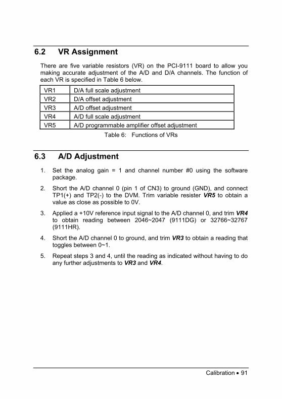
Calibration • 91
6.2 VR Assignment There are five variable resistors (VR) on the PCI-9111 board to allow you making accurate adjustment of the A/D and D/A channels. The function of each VR is specified in Table 6 below.
VR1 D/A full scale adjustment VR2 D/A offset adjustment VR3 A/D offset adjustment VR4 A/D full scale adjustment VR5 A/D programmable amplifier offset adjustment
Table 6: Functions of VRs
6.3 A/D Adjustment 1. Set the analog gain = 1 and channel number #0 using the software
package.
2. Short the A/D channel 0 (pin 1 of CN3) to ground (GND), and connect TP1(+) and TP2(-) to the DVM. Trim variable resister VR5 to obtain a value as close as possible to 0V.
3. Applied a +10V reference input signal to the A/D channel 0, and trim VR4 to obtain reading between 2046~2047 (9111DG) or 32766~32767 (9111HR).
4. Short the A/D channel 0 to ground, and trim VR3 to obtain a reading that toggles between 0~1.
5. Repeat steps 3 and 4, until the reading as indicated without having to do any further adjustments to VR3 and VR4.
92 • Calibration
6.4 D/A Adjustment
6.4.1 Unipolar Analog Output 1. Set JP1 to select uni-polar. Connect the DVM (+) to CN3 pin-30 (DAOut)
and DVM (-) to A.GND.
2. Write the digital value 0 to the DAC. Trim VR2 to obtain a 0V reading on the DVM
3. Write the digital value 4095 to the DAC. Trim VR1 to obtain a 10V reading on the DVM.
6.4.2 Bipolar Analog Output 1. Set JP1 to select bipolar. Connect the DVM (+) to CN3 pin-30 (DAOut)
and DVM (-) to A.GND.
2. Write the digital value 2048 to the DAC. Trim VR2 to obtain a 0V reading on the DVM.
3. Write the digital value 4095 to the DAC. Trim VR1 to obtain a +10V reading on the DVM.
A calibration utility is included with the ADLINK CD, which is included with the product package. A detailed calibration procedure and description can be found in the utility. Users only need to run the software calibration utility and follow the procedures.
Note: When you first receive the PCI-9112 card, calibration is NOT necessary, the PCI-9111 has been fully calibrated before it is shipped.
Software Utility • 93
7
Software Utility
The software CD provides two utility programs, the 9111util.exe and I_eeprom. The 9111util.exe provides three functions. It is used for system configuration, calibration, and Functional Testing. The I_eeprom utility is used to enable or disable interrupt of PCI-9111 board. Both utility programs are described in this chapter.
7.1 9111util.exe There are 3 functions provided by the 9111util.exe. It used for system configuration, calibration, and functional testing. This utility software is designed with a menu-driven based Windows environment. It provides text messages and graphical indicators for operating guidance.
7.1.1 Running 9111util.exe After finishing the DOS installation, you can execute the utility by typing the following command:
C> cd \ADLINK\DOS\9111\Util
C> 9111UTIL
The following displayed will appear on your screen. The message at the bottom of each window guides you through the selected item, follow the on screen instructions to change/set a value.
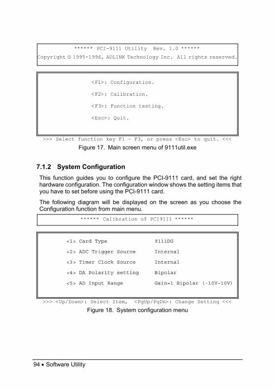
94 • Software Utility
****** PCI-9111 Utility Rev. 1.0 ******
Copyright © 1995-1996, ADLINK Technology Inc. All rights reserved.
<F1>: Configuration. <F2>: Calibration. <F3>: Function testing. <Esc>: Quit.
>>> Select function key F1 ~ F3, or press <Esc> to quit. <<<
Figure 17. Main screen menu of 9111util.exe
7.1.2 System Configuration This function guides you to configure the PCI-9111 card, and set the right hardware configuration. The configuration window shows the setting items that you have to set before using the PCI-9111 card.
The following diagram will be displayed on the screen as you choose the Configuration function from main menu.
****** Calibration of PCI9111 ******
<1> Card Type 9111DG <2> ADC Trigger Source Internal <3> Timer Clock Source Internal <4> DA Polarity setting Bipolar <5> AD Input Range Gain=1 Bipolar (-10V~10V)
>>> <Up/Down>: Select Item, <PgUp/PgDn>: Change Setting <<<
Figure 18. System configuration menu
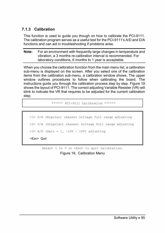
Software Utility • 95
7.1.3 Calibration This function is used to guide you though on how to calibrate the PCI-9111. The calibration program serves as a useful test for the PCI-9111's A/D and D/A functions and can aid in troubleshooting if problems arise.
Note: For an environment with frequently large changes in temperature and vibration, a 3 months re-calibration interval is recommended. For laboratory conditions, 6 months to 1 year is acceptable.
When you choose the calibration function from the main menu list, a calibration sub-menu is displayed on the screen. After you select one of the calibration items from the calibration sub-menu, a calibration window shows. The upper window outlines procedures to follow when calibrating the board. The instructions guide you through the calibration process step by step. Figure 19 shows the layout of PCI-9111. The correct adjusting Variable Resister (VR) will blink to indicate the VR that requires to be adjusted for the current calibration step.
****** PCI-9111 Calibration ******
<1> D/A (Bipolar) channel voltage full range adjusting <2> D/A (Unipolar) channel voltage full range adjusting <3> A/D (Gain = 1, -10V ~ 10V) adjusting <Esc> Quit
Select 1 to 3 or <Esc> to quit calibration.
Figure 19. Calibration Menu
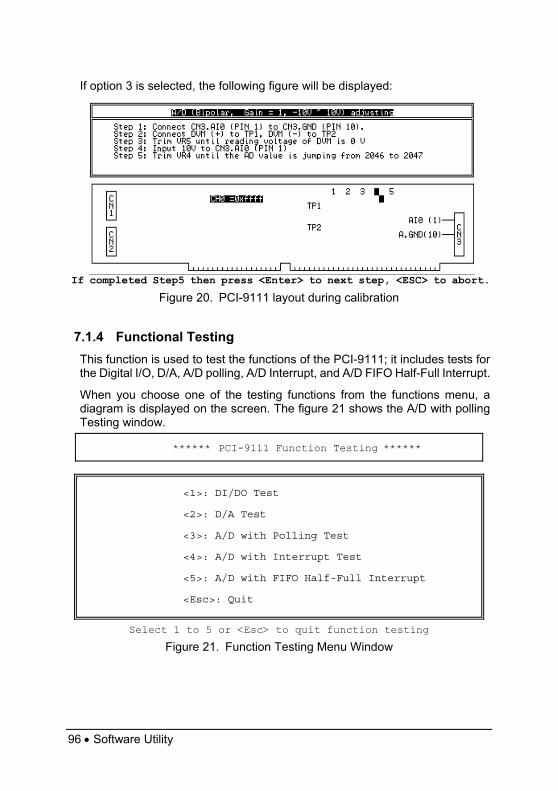
96 • Software Utility
If option 3 is selected, the following figure will be displayed:
If completed Step5 then press <Enter> to next step, <ESC> to abort. Figure 20. PCI-9111 layout during calibration
7.1.4 Functional Testing This function is used to test the functions of the PCI-9111; it includes tests for the Digital I/O, D/A, A/D polling, A/D Interrupt, and A/D FIFO Half-Full Interrupt.
When you choose one of the testing functions from the functions menu, a diagram is displayed on the screen. The figure 21 shows the A/D with polling Testing window.
****** PCI-9111 Function Testing ******
<1>: DI/DO Test <2>: D/A Test <3>: A/D with Polling Test <4>: A/D with Interrupt Test <5>: A/D with FIFO Half-Full Interrupt <Esc>: Quit
Select 1 to 5 or <Esc> to quit function testing
Figure 21. Function Testing Menu Window
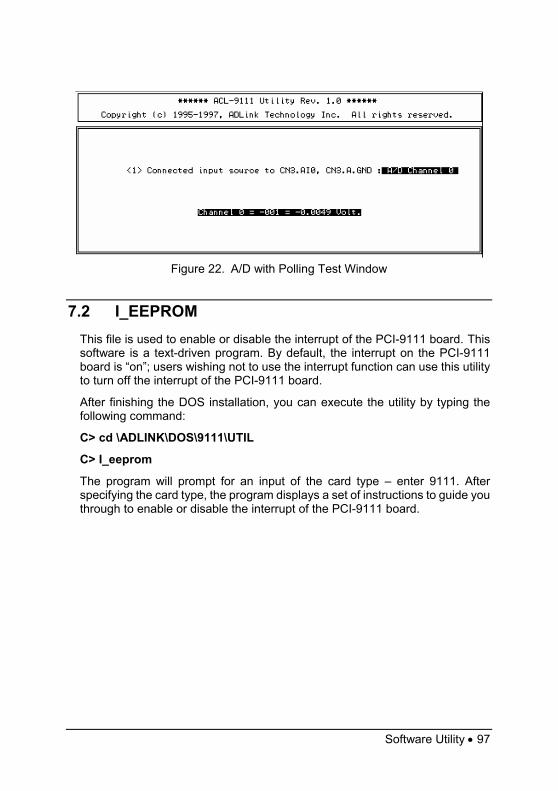
Software Utility • 97
Figure 22. A/D with Polling Test Window
7.2 I_EEPROM This file is used to enable or disable the interrupt of the PCI-9111 board. This software is a text-driven program. By default, the interrupt on the PCI-9111 board is “on”; users wishing not to use the interrupt function can use this utility to turn off the interrupt of the PCI-9111 board.
After finishing the DOS installation, you can execute the utility by typing the following command:
C> cd \ADLINK\DOS\9111\UTIL
C> I_eeprom
The program will prompt for an input of the card type – enter 9111. After specifying the card type, the program displays a set of instructions to guide you through to enable or disable the interrupt of the PCI-9111 board.
98 • Warranty Policy
Warranty Policy
Thank you for choosing ADLINK. To understand your rights and enjoy all the after-sales services we offer, please read the following carefully. 1. Before using ADLINK’s products please read the user manual and follow the
instructions exactly. When sending in damaged products for repair, please attach an RMA application form which can be downloaded from: http://rma.adlinktech.com/policy/.
2. All ADLINK products come with a limited two-year warranty, one year for products bought in China.
• The warranty period starts on the day the product is shipped from ADLINK’s factory.
• Peripherals and third-party products not manufactured by ADLINK will be covered by the original manufacturers' warranty.
• For products containing storage devices (hard drives, flash cards, etc.), please back up your data before sending them for repair. ADLINK is not responsible for any loss of data.
• Please ensure the use of properly licensed software with our systems. ADLINK does not condone the use of pirated software and will not service systems using such software. ADLINK will not be held legally responsible for products shipped with unlicensed software installed by the user.
• For general repairs, please do not include peripheral accessories. If peripherals need to be included, be certain to specify which items you sent on the RMA Request & Confirmation Form. ADLINK is not responsible for items not listed on the RMA Request & Confirmation Form.
3. Our repair service is not covered by ADLINK's guarantee in the following situations:
• Damage caused by not following instructions in the User's Manual. • Damage caused by carelessness on the user's part during product
transportation. • Damage caused by fire, earthquakes, floods, lightening, pollution,
other acts of God, and/or incorrect usage of voltage transformers.

Warranty Policy • 99
• Damage caused by inappropriate storage environments such as with high temperatures, high humidity, or volatile chemicals.
• Damage caused by leakage of battery fluid during or after change of batteries by customer/user.
• Damage from improper repair by unauthorized ADLINK technicians.
• Products with altered and/or damaged serial numbers are not entitled to our service.
• This warranty is not transferable or extendible. • Other categories not protected under our warranty.
4. Customers are responsible for all fees necessary to transport damaged products to ADLINK.
For further questions, please e-mail our FAE staff: [email protected]