Embed Size (px)
Citation preview

Condensed MatterJournal of Physics:
Top Papers 2003 Showcase highlights the leading and most frequently downloadedpapers, letters and topical reviews to Journal of Physics: Condensed Matter, arguably theworld’s most authoritative source of topical information for condensed matter physicistsand materials and surface scientists. Journal of Physics: Condensed Matter coversexperimental and theoretical studies of thestructural, thermal, mechanical, electrical,magnetic and optical properties of condensedmatter and is published 50 times per year byInstitute of Physics Publishing.
TOP PAPERS 2003
CO N D E N S E D MAT T E R: TOP PAPERS 2003 SHOWCASE 1
PU B L I S H E D B Y IN S T I T U T E O F PH YS I C S PU B L I S H I N G
S H O W C A S E
Mesomagnetism 10C L Dennis, R P Borges, L D Buda, U Ebels, J F Gregg,M Hehn, E Jouguelet, K Ounadjela, I Petej, I LPrejbeanu and M J Thornton
Organic electronics 10S R Forrest
Nanostructures from nanoparticles 10Paula M Mendes, Yu Chen, Richard E Palmer, KirillNikitin, Donald Fitzmaurice and Jon A Preece
Magnetism of films, stripes and dots 11J Shen, J P Pierce, E W Plummer and J Kirschner
Spin-dependent tunnelling 11Evgeny Y Tsymbal, Oleg N Mryasov and Patrick R LeClair
Atom lithography 11Markus K Oberthaler and Tilman Pfau
Relaxor ferroelectrics 12George A Samara
Nanomagnetics 12R Skomski
R E V I E W S
We welcome papers and submissions fromauthors who have research interests in theseareas. Authors can benefit from rapid receipt-to-publication times, a rising impact factorand a large and growing world widereadership both in print and on-line. On average papers are downloaded on-line over100 times via our award winning ElectronicJournals service.For more information on the submissionprocess and to view the latest publishedpapers from Journal of Physics: CondensedMatter visit www.iop.org/EJ/journal/JPhysCM
P A P E R S
Inside you will find synopses of all the top papers and reviews listedabove, together with details of where to find the full articles Ł Ł Ł Ł
Magnetic nanostructures 2C Binns, F Sirotti, H Cruguel, S H Baker, P Prieto, J D Bellier and S C Thornton
Microstructure of gels 2S A Shah, Y-L Chen, S Ramakrishnan, K S Schweizer and C F Zukoski
Oxidation of nanotubes 2T Savage, S Bhattacharya, B Sadanadan, J Gaillard, T M Tritt, Y-P Sun,Y Wu, S Nayak, R Car, N Marzari, P M Ajayan and A M Rao
Focusing light using negative refraction 3J B Pendry and S A Ramakrishna
Quantum transport in nanowires 3D M Gillingham, C Müller and J A C Bland
Silicon-based quantum gates 3A M Stoneham, A J Fisher and P T Greenland
Nanoscale cracks in glass 4Christian Marlière, Silke Prades, Fabrice Célarié, Davy Dalmas, Daniel Bonamy,Claude Guillot and Elisabeth Bouchaud
Microscopy of amorphous materials 4R K Dash, P M Voyles, J M Gibson, M M J Treacy and P Klebinski
Laser modification of glass 4W Reichman, J W Chan and D M Krol
Magnetism in monatomic metal wires 5P Gambardella
Ferroelectric capacitor arrays 5M Dawber, I Szafraniak, M Alexe and J F Scott
Pettifor maps 5Dane Morgan, John Rodgers and Gerbrand Ceder
Quantum condensation of liquid 4He 6Mark Brown and Adrian F G Wyatt
‘Hot’ spin ice 6G Ehlers, A L Cornelius, M Orendác, M Kajnaková, T Fennell, S T Bramwell and J S Gardner
Magnetism of metal clusters 6Yuannan Xie and John A Blackman
Photonic minibands 7M A Kaliteevski, J Manzanares Martinez, D Cassagne, J P Albert, S Brand and R A Abram
Polarons in high-Tc superconductors 7A R Bishop, D Mihailovic and J Mustre de León
Self-organized criticality in friction 7Fredy R Zypman, John Ferrante, Mark Jansen, Kathleen Scanlon and Phillip Abel
Photoluminescence in mesoporous nanotubes 8Finlay D Morrison, Laura Ramsay and James F Scott
Ferroelectric nanotubes 8J L Shen, Y C Lee, Y L Lui, P W Cheng and C F Cheng
Landauer formula without Landauer’s assumptions 8Mukunda P Das and Frederick Green
Encapsulated magnetite particles for biomedical application 9Katharina Landfester and Liliana P Ramírez
Self-trapped states in proteins? 9Robert H Austin, Aihua Xie, Lex van der Meer, Michelle Shinn and George Neil
A new superconductor 9S Yonezawa, Y Muraoka, Y Matsushita and Z Hiroi

2 CO N D E N S E D MAT T E R: TOP PAPERS 2003 SHOWCASE
Magnetic nanostructuresStatic and dynamic magnetic behaviour ofiron nanoclusters on magnetic substratesC Binns, F Sirotti, H Cruguel,S H Baker, P Prieto, J D Bellier and S C Thornton J. Phys.: Condens. Matter 15 No 25 (2 July 2003) 4287–4299
In magnetic nanoparticles containing a few to a fewthousand atoms, the exchange length is significantcompared to the cluster diameter. This produces anumber of interesting and technically useful effects,e.g. in magnetic recording applications. Even whendeposited on a surface or embedded in a matrix, 3dtransition metal clusters have a significantly highermagnetic moment per atom relative to the bulk. CBinns’ group at Leicester with co-workers at LUREOrsay, Sincrotrone Trieste and Madrid report staticand dynamic measurements of Fe nanoclusters of140–270 atoms, deposited in situ onto amorphousvitrovac substrates, using a gas aggregation source.Magnetic behaviour was determined specificallywithin the Fe clusters, independent of the substrate orcoating materials.
Magnetic linear dichroism in the angulardistribution (MLDAD) of the Fe 3p core levelphotoemission gave the static magnetization of thecluster films in the exchange field of the substrates asa function of coverage. The switching dynamics werestudied on the nanosecond timescale by time-resolved spin-polarized photoemission. TheMLDAD signal at saturation of dense cluster filmswith several cluster layers was ~5% higher than anMBE-grown film, indicating an enhanced spinmoment even when clusters are in contact. Coatingan exposed sub-monolayer cluster layer with Coincreases the Fe MLDAD signal by 35%, indicating asubstantially increased magnetic moment within theFe clusters. At low coverages, below the percolationthreshold, the sample showed the same switchingdynamics as in the clean substrate. Near thepercolation threshold, however, a significantacceleration of the magnetic reversal was seen, with afast component due to a reversal propagating throughthe cluster film. On average, each cluster switches inabout 10 ns.
Microstructure of gels Microstructure of dense colloid–polymersuspensions and gelsS A Shah, Y-L Chen, S Ramakrishnan,K S Schweizer and C F Zukoski J. Phys.: Condens. Matter 15 No 27 (16 July 2003) 4751–4778
Suspensions which undergo a fluid-to-gel transitionare of enormous technological significance, partlybecause the gel microstructure and mechanicalproperties can be controlled. Recent studies showthat gels can form from the homogeneous fluid phasewith increasing strength of interparticle attractionwhen the range of the attraction is less than about atenth of a particle radius, R. The suspension flowproperties change from liquid-like to solid-like, sincerelaxation times grow to be longer than times ofexperimental observation. The material displays adynamic yield stress.
A gel is a non-ergodic, space-filling soft solid wherelong-range diffusive motion is arrested. A modelsystem for systematically changing the strength andrange of the interparticle attractions exploitsdepletion attractions between hard-sphere particlesby adding non-adsorbing polymers. When thepolymer radius of gyration is much less than theparticle radius, the range of the induced attraction issmall. At polymer concentrations well below wherepolymer coils begin to overlap, the suspensions gel.This non-equilibrium transition can pre-empt theequilibrium fluid–fluid and fluid–crystal phasetransitions, or occur in a two-phase coexistenceregion. Gelation bears some similarities to the hard-sphere glass transition which occurs at a particlevolume fraction of about 0.58.
C Zukowski’s group at Urbana describesmeasurements of the collective structure factor ofdense colloidal suspensions in the fluid and gel statesproduced by adding small non-adsorbing polymersuch that the radius of gyration lies between 5% and8% of R. Pinhole-collimated ultra-small-angle x-rayscattering (USAXS) is employed. As the polymerconcentration is increased at fixed volume fraction,excellent quantitative agreement is demonstrated inthe fluid phase with the parameter-free predictions ofPRISM theory. Above the polymer concentration atwhich gels are produced, agreement is poor, showingthe suspensions have fallen out of equilibrium. Upongelation, the local cage structure is frozen,intermediate-scale fluctuations are suppressed andlarge small-wavevector fluctuations emerge due toheterogeneities or 'clusters'.
Oxidation of nanotubesPhotoinduced oxidation of carbon nanotubesT Savage, S Bhattacharya, B Sadanadan,J Gaillard, T M Tritt, Y-P Sun, Y Wu, S Nayak,R Car, N Marzari, P M Ajayan and A M Rao J. Phys.: Condens. Matter 15 No 35 (10 September 2003) 5915–5921
In single-walled carbon nanotube (SWNT) bundles,the sign of the thermopower proves extremelysensitive to oxygen adsorption. This has implicationsfor practical carbon nanotube field effect transistors(CNFETs). At room temperature, thermopowervalues are around +45 µV K-1 in 'mats' of SWNTbundles doped to saturation under ambientconditions with oxygen. When oxygen is desorbedfrom the SWNT bundles at temperatures from350–500 K and high vacuum (10-5-10-8 Torr) overtimes from 30 minutes to 12 hours, the thermopowerswitches reversibly to an n-type value of about �50µV K-1. The time evolution from negativethermopower values in oxygen-desorbed SWNTmats to positive thermopower values, under ambientconditions, has a characteristic value varying from afew minutes to hours, depending on the matthickness. Recently, p-type CNTFETs were found toconvert to n-CNTFETs when annealed in vacuum.Upon re-exposure to oxygen, the p-CNTFETproperties were recovered.
S Nayak’s group at Rensselaer Polytechnic Institutewith co-workers at Clemson, Princeton and MIThave published thermopower measurements showingthat carbon nanotubes, when exposed simultaneouslyto UV light and oxygen, exhibit photoinducedoxidation. This they relate to a theoretical analysis forboth graphene and nanotube structures with limiteddefect types. At least two plausible mechanisms forthe experimentally observed photoinduced oxidationare proposed: (i) a lower energy barrier for theadsorption of photo-generated singlet oxygen, or (ii)the presence of defects in carbon nanotubes that mayfacilitate the formation of locally electron-deficientand electron-rich regions on the nanotubes, and thesefacilitate the adsorption of oxygen molecules on thenanotubes. Experiments with magnetic fields, likeelectron spin resonance (ESR), could further confirmthe proposed mechanisms. Thus, the ESR of carbonnanotubes oxidized in the presence of UV lightshould show relatively higher concentrations ofsinglet oxygen compared to nanotubes oxidizedunder room light.
Condensed Matter:Top Papers 2003 Showcase
Schematic diagram of the molecular field within Fe clusters adsorbed
on vitrovac due to the exchange interaction at the contact point between
the clusters and the substrate.
Plots of binding energy of O2 with a (10, 0) nanotube as a function
of the molecule’s distance D (Å) from the nanotube surface. The
binding energy of the physisorbed T state is about 0.004 eV at 3.7 Å
(not shown here). The inset shows a ball and stick picture of O2(large atoms) bonded to a 7–5–5–7 (small atoms) defect site.
An illustration of (A) a hard-sphere solution and (B)
interpenetrating, polydisperse, dense percolated clusters of an average
size �c. The surrounding voids or heterogeneities have a characteristic
length of �v ~ 5–8D where D is the colloid diameter. Also shown is a
schematic illustrating changes in the structural correlations as
equilibrium fluids transform to dense gels.
CO N D E N S E D MAT T E R: TOP PAPERS 2003 SHOWCASE 3
Focusing light using negative refractionJ B Pendry and S A RamakrishnaJ. Phys.: Condens. Matter 15 No 37 (24 September 2003) 6345–6364
Conventional lenses suffer from a fundamentallimitation of resolution: no details finer than thewavelength of radiation can be resolved. Negativerefraction lenses could do much better, and are justone example of possible novel optical devices.
Some time ago V G Veselago observed that if itwere possible to realize materials with permittivity,M, and permeability, µ, both equal to �1, then arefractive index of n = �1 would result and a slab ofthe material would focus light. A negative refractionlens works according to quite different principlesfrom a conventional lens: it builds on the idea that anegatively refracting slab, n = �1, is in some sensecomplementary to an equal thickness of vacuum andcancels its presence. This cancellation is unusuallycomplete because the compensating effect of the slabextends not only to the radiative component of thefield, but also to the evanescent near field whichconveys the sub-wavelength details of the image.Ordinary lenses do not capture the near field, hencethe limitations to their resolution. Lenses with thissub-wavelength focusing property are referred to as'perfect lenses'.
The cancellation by a slab of thickness d is a specialcase of a much wider class of focusing: any mediumcan be optically cancelled by an equal thickness ofmaterial constructed to be an inverted mirror imageof the medium, with M, T reversed in sign. J B Pendryand S A Ramakrishna of Imperial College, Londonintroduce the powerful technique of coordinatetransformation, mapping a known system into anequivalent system, so as to extend the result to a muchwider class of structures including cylinders, spheresand intersecting planes, and hence show how toproduce magnified images. All the images are'perfect' in the sense that both the near and far fieldsare brought to a focus and hence reveal sub-wavelength details. The technique used in provingthese results, the equivalence of coordinatetransformations to a change in M and µ, is a powerfuland widely applicable tool which is expected togenerate even more results in the future.
Quantum transport in nanowiresSpin-dependent quantum transport effects in Cu nanowiresD M Gillingham, C Müller and J A C BlandJ. Phys.: Condens. Matter 15 No 19 (21 May 2003) L291–L296
Underlying spintronics is the proposal to use the spinof the electron instead of its electrical charge infuture devices. The challenge is to achieve efficientspin injection at room temperature and todemonstrate the manipulation of electron spin in anall-electrical manner conclusively. Spintronicsrequires small structures to ensure that the spins actcoherently, and that the electrons travel ballistically.Low-dimensional structures such as nanowires canhave an electronic structure vastly different from thatof the bulk material. This can be expected to behighly significant in the operation of spintronicdevices.
J A C Bland’s group at Cambridge has observedmagnetic field-dependent quantum transport incopper nanowires. A large magnetoconductanceeffect arises, attributed to the formation of spin-splitconduction states in the nanowire. A significantmagneto-conductance effect in copper nanowires infields of 2 mT is seen, and interpreted as being due tothe spin filtering effect introduced by oxygenadsorbates modifying the electronic band structure inthe nanowire. By reducing the dimensions of theactive material, they find surprisingly large spin-polarized quantum conduction effects in a materialwhich is non-magnetic in the bulk. This may offer anew approach in developing spintronic devices,differing from the current research effort devoted todeveloping bulk materials which have 100% spinpolarization. This effect could be seen in other non-magnetic metals when formed into nanowires underthe correct conditions.
Silicon-based quantum gatesOptically driven silicon-based quantum gateswith potential for high-temperature operationA M Stoneham, A J Fisher and P T GreenlandJ. Phys.: Condens. Matter 15 No 27 (16 July 2003) L447–L451
In quantum information processing, challengesinclude quantum information storage as qubits, andquantum information manipulation. For quantuminformation manipulation, it suffices to have twotypes of universal gate: the so-called A-gates, thatmanipulate individual qubits, and the so-called J-gates, that control the quantum dance of one qubitwith another. There would be major practicaladvantages if the universal quantum gates satisfiedtwo practical criteria, namely that the processorshould be silicon compatible, ideally one that mightbe built by largely off-the-shelf methods, andsecondly that the decoherence mechanisms and keyenergies should be such as to allow operation at usefultemperatures, ideally at room temperature, alongsideconventional classical devices. Quantum behaviour isnot an intrinsically low-temperature phenomenon.Certainly, for near-equilibrium behaviour, governedby quantum statistics, high temperatures makequantal effects less and less evident. But quantuminformation processing aims to stay far fromequilibrium, and quantum dynamics can remain veryimportant at higher temperatures. Practical issuesmay be serious, of course, as the approach toequilibrium may be fast.
A M Stoneham’s group at University CollegeLondon propose a new approach to constructinggates for quantum information processing, exploitingthe properties of impurities in silicon. Quantuminformation, embodied in electron spins bound todeep donors, is coupled via optically inducedelectronic excitation. Gates are manipulated bymagnetic fields and optical light pulses; individualgates are addressed by exploiting spatial andspectroscopic selectivity. These qubits are distributedin space such that mutual interactions are small in thenormal (ground) state, in which they are able to storequantum information. In an electronic excited state,however, entangling interactions between qubits canoccur. Only in excited states are pairs of qubitsmanipulated. Their approach therefore relies onknowing the natures of the excited states and onengineering the system so as to optimize these states.Such quantum gates do not rely on small energyscales for operation, so might function at or nearroom temperature. They show the scheme canproduce the classes of gates necessary to construct auniversal quantum computer.
Condensed Matter:Top Papers 2003 Showcase
An alternative pair of complementary media, each cancelling the
effect of the other. The light does not necessarily follow a straight line
path in each medium, but the overall effect is as if a section of space
thickness 2d were removed from the experiment. These are representative conduction histograms. They are built up
from conductance versus time curves taken at room temperature in air.
(A) was taken at zero applied magnetic field—it shows that the
expected 2e 2/h quantization is dominant; however, there is a small
peak at 0.5 � 2e 2/h and one at 1.5 � 2e 2/h, showing that there is
some quantization in units of e 2/h occurring. (B) was taken with a
0.5 mT magnetic field applied perpendicular to the nanowire—it
shows that the e 2/h quantization has become far more dominant than
in (A), the zero-field case. The inset is a schematic diagram of the
field direction with respect to the nanowire.
Quantum information is encoded in the electron spins of deep donors
(red) in a silicon layer, the spins being manipulated optically.
Entanglement is controlled using optical excitation and de-excitation
of electrons from control atoms (blue rings).
4 CO N D E N S E D MAT T E R: TOP PAPERS 2003 SHOWCASE
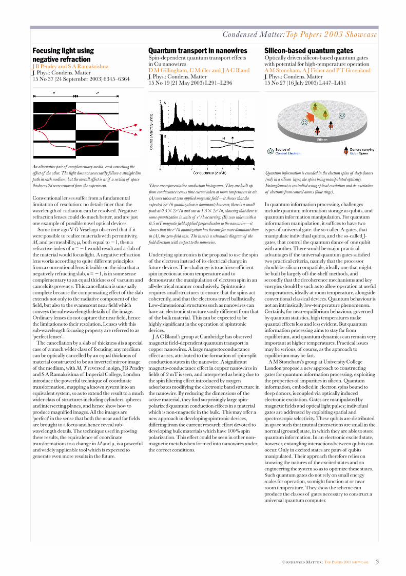
Nanoscale cracks in glassCrack fronts and damage in glass at the nanometre scaleChristian Marlière, Silke Prades, FabriceCélarié, Davy Dalmas, Daniel Bonamy, ClaudeGuillot and Elisabeth BouchaudJ. Phys.: Condens. Matter 15 No 31 (13 August 2003) S2377–S2386
Materials fracture exhibits many puzzling aspects. Itis especially hard to reconcile two differentobservations. Brittle materials (glass is a commonexample) break abruptly, without first deforming,whereas large plastic deformations precede fracture inductile materials (like most metal alloys). In ductilefracture, the crack progresses through the coalescenceof micrometric damage cavities nucleated frommicrostructural defects (second phase precipitates,grain boundaries . . .). Yet quantitative studies showboth types of fracture surfaces to have a very similarmorphology. Fracture surfaces are self-affine objectsboth for brittle and for ductile materials. Two self-affine regimes coexist: at small length scales (up to alength Vc), the roughness exponent N is close to 0.5 forlength scales below a characteristic length Vc, whereasN is around 0.8 for larger length scales, up to a lengthV. These values of N are universal, but Vc and Vdepend on the kind of material considered. Valuesrange from a few nanometers for glass to a fewcentimetres for concrete and rocks. For ductilematerials, Vc is of the order of the typical size of thedamage cavities when they coalesce. This stronglysuggests that the observed transition between the twoself-affine regimes reflects a change from an intra-cavity structure to an inter-cavity one.
A natural supposition is that there might be anundetected ductile-like fracture process in brittlematerials like glass. If so, the size of the associateddamage cavities at coalescence would be comparablewith the crossover length Vc, of order 10 nm. Groupsheaded by C Marlière at Montpellier and E Bouchaudat Saclay sought to observe such an effectexperimentally using atomic force microscopy. Hugevelocity fluctuations in the progression of the tip weredetected and explained by the observation ofnanometric cavities developing ahead of the crack tip.That these were damage cavities was confirmed byusing two independent methods. Their resultsconfirm the scenario previously proposed byBouchaud et al to explain the origin of the two self-affine regimes observed on fracture surfaces. The factthat glass, even at temperatures far below the glasstransition temperature Tg, joins the class ofdamageable materials should have importantconsequences. The design of structures using glassmight be modified to take this behaviour into account,especially for slow crack propagation processes. Thesimilarity between the damage modes of materials asdifferent as glass and metallic alloys is an importantclue to aid our understanding of the origin of somepuzzling universal behaviour, and sheds new light onthe basic physical mechanisms of fracture.
Microscopy of amorphous materialsA quantitative measure of medium-range orderin amorphous materials from transmission electron micrographsR K Dash, P M Voyles, J M Gibson,M M J Treacy and P Klebinski.J. Phys.: Condens. Matter 15 No 31 (13 August 2003) S2425–S2435
Understanding of the properties of amorphous andglassy materials has been hindered by incompleteknowledge of their atomic structure, especiallybeyond the shortest-range features. Diffractionexperiments give the structure factor S(k), and henceits Fourier transform g2(r), which gives the probabilityof finding two atoms in the sample separated by adistance r. But g2(r) is not very sensitive to medium-range order (MRO) present in many amorphousmaterials at the nm scale. Evidence for MRO comesfrom the anomalous first sharp diffraction peak foundfor many ionic and covalent glasses and from small-angle scattering. MRO is believed to affect diffusive,mechanical, optical and electronic properties ofamorphous materials, such as the optoelectronicproperties of amorphous silicon for solar-cell and flatpanel display applications, known to deteriorate withexposure to light.
M M J Treacy (NEC, Princeton) and J M Gibson(Argonne) developed fluctuation electron microscopy(FEM) to provide more information about MRO inamorphous materials. FEM is the statistical analysisof fluctuations in diffraction from nanometre-scalevolumes. Such local diffraction can be measured bytransmission electron microscopy (TEM). Higher-order atomic distribution functions, more sensitive tomedium-range structure than g2(r), contribute toFEM observations. Treacy and Gibson together withP M Voyles of University of Wisconsin, Madison andR K Dash and P Keblinski of Rensselaer PolytechnicInstitute propose a new quantitative measure ofMRO in amorphous materials, related to FEM. Thespatial autocorrelation function of dark-field TEMimage intensities shows an exponential decay. Thedecay length is determined by an intrinsic structuralcorrelation length and the microscope resolution.The analysis indicates that measurements at a fewdiscrete resolutions are sufficient to separate theseeffects and determine the intrinsic correlation length.This measure of MRO is demonstrated in simulatedimages from computer-generated models of a-Si andin experimental images of a-Si. The correlationlength from the simulations follows the degree ofmedium-range order introduced a priori into themodels. The correlation length in the experimentsshows the same trend as previous FEMmeasurements for the same samples.
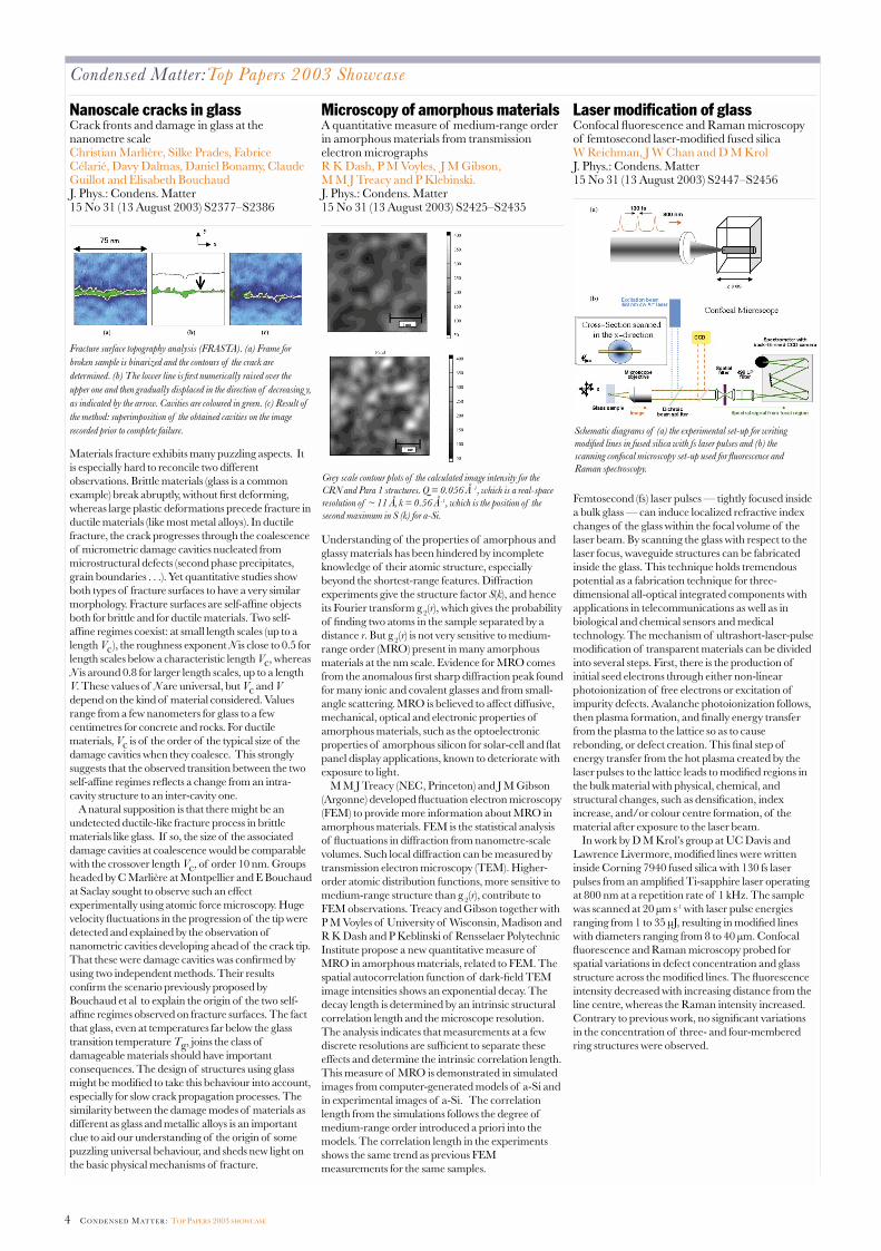
Laser modification of glassConfocal fluorescence and Raman microscopyof femtosecond laser-modified fused silicaW Reichman, J W Chan and D M Krol J. Phys.: Condens. Matter 15 No 31 (13 August 2003) S2447–S2456
Femtosecond (fs) laser pulses — tightly focused insidea bulk glass — can induce localized refractive indexchanges of the glass within the focal volume of thelaser beam. By scanning the glass with respect to thelaser focus, waveguide structures can be fabricatedinside the glass. This technique holds tremendouspotential as a fabrication technique for three-dimensional all-optical integrated components withapplications in telecommunications as well as inbiological and chemical sensors and medicaltechnology. The mechanism of ultrashort-laser-pulsemodification of transparent materials can be dividedinto several steps. First, there is the production ofinitial seed electrons through either non-linearphotoionization of free electrons or excitation ofimpurity defects. Avalanche photoionization follows,then plasma formation, and finally energy transferfrom the plasma to the lattice so as to causerebonding, or defect creation. This final step ofenergy transfer from the hot plasma created by thelaser pulses to the lattice leads to modified regions inthe bulk material with physical, chemical, andstructural changes, such as densification, indexincrease, and/or colour centre formation, of thematerial after exposure to the laser beam.
In work by D M Krol’s group at UC Davis andLawrence Livermore, modified lines were writteninside Corning 7940 fused silica with 130 fs laserpulses from an amplified Ti-sapphire laser operatingat 800 nm at a repetition rate of 1 kHz. The samplewas scanned at 20 µm s-1 with laser pulse energiesranging from 1 to 35 µJ, resulting in modified lineswith diameters ranging from 8 to 40 µm. Confocalfluorescence and Raman microscopy probed forspatial variations in defect concentration and glassstructure across the modified lines. The fluorescenceintensity decreased with increasing distance from theline centre, whereas the Raman intensity increased.Contrary to previous work, no significant variationsin the concentration of three- and four-memberedring structures were observed.
Condensed Matter:Top Papers 2003 Showcase
Fracture surface topography analysis (FRASTA). (a) Frame for
broken sample is binarized and the contours of the crack are
determined. (b) The lower line is first numerically raised over the
upper one and then gradually displaced in the direction of decreasing y,
as indicated by the arrow. Cavities are coloured in green. (c) Result of
the method: superimposition of the obtained cavities on the image
recorded prior to complete failure. Schematic diagrams of (a) the experimental set-up for writing
modified lines in fused silica with fs laser pulses and (b) the
scanning confocal microscopy set-up used for fluorescence and
Raman spectroscopy.Grey scale contour plots of the calculated image intensity for the
CRN and Para 1 structures. Q = 0.056 Aº -1, which is a real-space
resolution of ~ 11 Aº, k = 0.56 Aº -1, which is the position of the
second maximum in S (k) for a-Si.
CO N D E N S E D MAT T E R: TOP PAPERS 2003 SHOWCASE 5
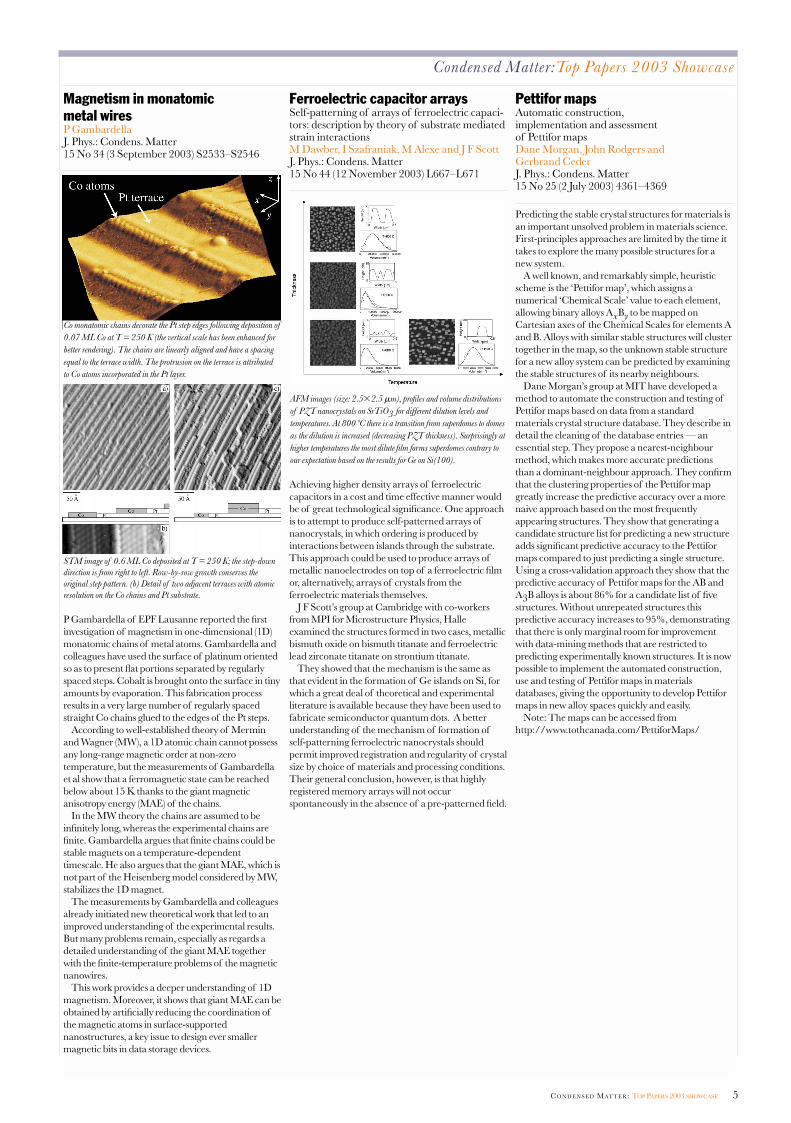
Magnetism in monatomic metal wiresP GambardellaJ. Phys.: Condens. Matter 15 No 34 (3 September 2003) S2533–S2546
P Gambardella of EPF Lausanne reported the firstinvestigation of magnetism in one-dimensional (1D)monatomic chains of metal atoms. Gambardella andcolleagues have used the surface of platinum orientedso as to present flat portions separated by regularlyspaced steps. Cobalt is brought onto the surface in tinyamounts by evaporation. This fabrication processresults in a very large number of regularly spacedstraight Co chains glued to the edges of the Pt steps.
According to well-established theory of Merminand Wagner (MW), a 1D atomic chain cannot possessany long-range magnetic order at non-zerotemperature, but the measurements of Gambardellaet al show that a ferromagnetic state can be reachedbelow about 15 K thanks to the giant magneticanisotropy energy (MAE) of the chains.
In the MW theory the chains are assumed to beinfinitely long, whereas the experimental chains arefinite. Gambardella argues that finite chains could bestable magnets on a temperature-dependenttimescale. He also argues that the giant MAE, which isnot part of the Heisenberg model considered by MW,stabilizes the 1D magnet.
The measurements by Gambardella and colleaguesalready initiated new theoretical work that led to animproved understanding of the experimental results.But many problems remain, especially as regards adetailed understanding of the giant MAE togetherwith the finite-temperature problems of the magneticnanowires.
This work provides a deeper understanding of 1Dmagnetism. Moreover, it shows that giant MAE can beobtained by artificially reducing the coordination ofthe magnetic atoms in surface-supportednanostructures, a key issue to design ever smallermagnetic bits in data storage devices.
Ferroelectric capacitor arraysSelf-patterning of arrays of ferroelectric capaci-tors: description by theory of substrate mediatedstrain interactionsM Dawber, I Szafraniak, M Alexe and J F Scott J. Phys.: Condens. Matter 15 No 44 (12 November 2003) L667–L671
Achieving higher density arrays of ferroelectriccapacitors in a cost and time effective manner wouldbe of great technological significance. One approachis to attempt to produce self-patterned arrays ofnanocrystals, in which ordering is produced byinteractions between islands through the substrate.This approach could be used to produce arrays ofmetallic nanoelectrodes on top of a ferroelectric filmor, alternatively, arrays of crystals from theferroelectric materials themselves.
J F Scott’s group at Cambridge with co-workersfrom MPI for Microstructure Physics, Halleexamined the structures formed in two cases, metallicbismuth oxide on bismuth titanate and ferroelectriclead zirconate titanate on strontium titanate.
They showed that the mechanism is the same asthat evident in the formation of Ge islands on Si, forwhich a great deal of theoretical and experimentalliterature is available because they have been used tofabricate semiconductor quantum dots. A betterunderstanding of the mechanism of formation ofself-patterning ferroelectric nanocrystals shouldpermit improved registration and regularity of crystalsize by choice of materials and processing conditions.Their general conclusion, however, is that highlyregistered memory arrays will not occurspontaneously in the absence of a pre-patterned field.
Pettifor mapsAutomatic construction,implementation and assessment of Pettifor mapsDane Morgan, John Rodgers and Gerbrand CederJ. Phys.: Condens. Matter 15 No 25 (2 July 2003) 4361–4369
Predicting the stable crystal structures for materials isan important unsolved problem in materials science.First-principles approaches are limited by the time ittakes to explore the many possible structures for anew system.
A well known, and remarkably simple, heuristicscheme is the ‘Pettifor map’, which assigns anumerical ‘Chemical Scale’ value to each element,allowing binary alloys AxBy to be mapped onCartesian axes of the Chemical Scales for elements Aand B. Alloys with similar stable structures will clustertogether in the map, so the unknown stable structurefor a new alloy system can be predicted by examiningthe stable structures of its nearby neighbours.
Dane Morgan’s group at MIT have developed amethod to automate the construction and testing ofPettifor maps based on data from a standardmaterials crystal structure database. They describe indetail the cleaning of the database entries — anessential step. They propose a nearest-neighbourmethod, which makes more accurate predictionsthan a dominant-neighbour approach. They confirmthat the clustering properties of the Pettifor mapgreatly increase the predictive accuracy over a morenaive approach based on the most frequentlyappearing structures. They show that generating acandidate structure list for predicting a new structureadds significant predictive accuracy to the Pettiformaps compared to just predicting a single structure.Using a cross-validation approach they show that thepredictive accuracy of Pettifor maps for the AB andA3B alloys is about 86% for a candidate list of fivestructures. Without unrepeated structures thispredictive accuracy increases to 95%, demonstratingthat there is only marginal room for improvementwith data-mining methods that are restricted topredicting experimentally known structures. It is nowpossible to implement the automated construction,use and testing of Pettifor maps in materialsdatabases, giving the opportunity to develop Pettiformaps in new alloy spaces quickly and easily.
Note: The maps can be accessed fromhttp://www.tothcanada.com/PettiforMaps/
Condensed Matter:Top Papers 2003 Showcase
Co monatomic chains decorate the Pt step edges following deposition of
0.07 ML Co at T = 250 K (the vertical scale has been enhanced for
better rendering). The chains are linearly aligned and have a spacing
equal to the terrace width. The protrusion on the terrace is attributed
to Co atoms incorporated in the Pt layer.
AFM images (size: 2.5�2.5 �m), profiles and volume distributions
of PZT nanocrystals on SrTiO3 for different dilution levels and
temperatures. At 800 ºC there is a transition from superdomes to domes
as the dilution is increased (decreasing PZT thickness). Surprisingly at
higher temperatures the most dilute film forms superdomes contrary to
our expectation based on the results for Ge on Si(100).
STM image of 0.6 ML Co deposited at T = 250 K; the step-down
direction is from right to left. Row-by-row growth conserves the
original step pattern. (b) Detail of two adjacent terraces with atomic
resolution on the Co chains and Pt substrate.
6 CO N D E N S E D MAT T E R: TOP PAPERS 2003 SHOWCASE
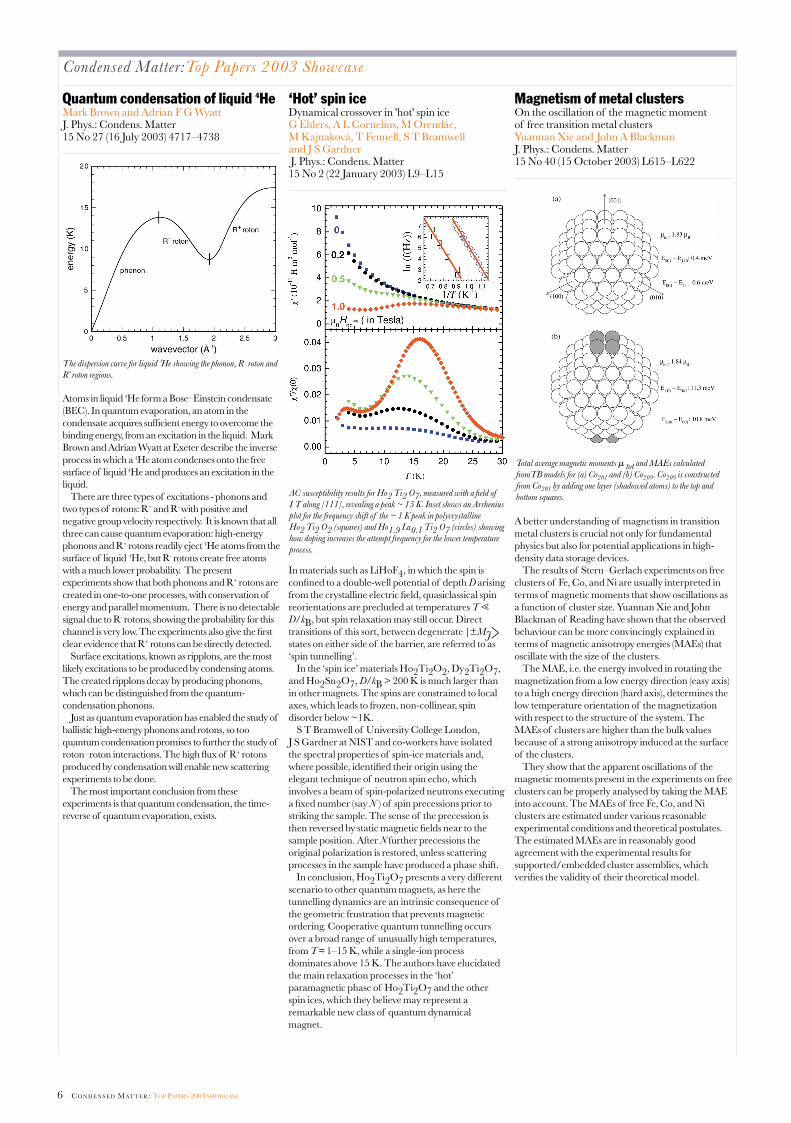
Quantum condensation of liquid 4HeMark Brown and Adrian F G WyattJ. Phys.: Condens. Matter 15 No 27 (16 July 2003) 4717–4738
Atoms in liquid 4He form a Bose–Einstein condensate(BEC). In quantum evaporation, an atom in thecondensate acquires sufficient energy to overcome thebinding energy, from an excitation in the liquid. MarkBrown and Adrian Wyatt at Exeter describe the inverseprocess in which a 4He atom condenses onto the freesurface of liquid 4He and produces an excitation in theliquid.
There are three types of excitations - phonons andtwo types of rotons: R+ and R- with positive andnegative group velocity respectively. It is known that allthree can cause quantum evaporation: high-energyphonons and R+ rotons readily eject 4He atoms from thesurface of liquid 4He, but R- rotons create free atomswith a much lower probability. The presentexperiments show that both phonons and R+ rotons arecreated in one-to-one processes, with conservation ofenergy and parallel momentum. There is no detectablesignal due to R- rotons, showing the probability for thischannel is very low. The experiments also give the firstclear evidence that R+ rotons can be directly detected.
Surface excitations, known as ripplons, are the mostlikely excitations to be produced by condensing atoms.The created ripplons decay by producing phonons,which can be distinguished from the quantum-condensation phonons.
Just as quantum evaporation has enabled the study ofballistic high-energy phonons and rotons, so tooquantum condensation promises to further the study ofroton–roton interactions. The high flux of R+ rotonsproduced by condensation will enable new scatteringexperiments to be done.
The most important conclusion from theseexperiments is that quantum condensation, the time-reverse of quantum evaporation, exists.
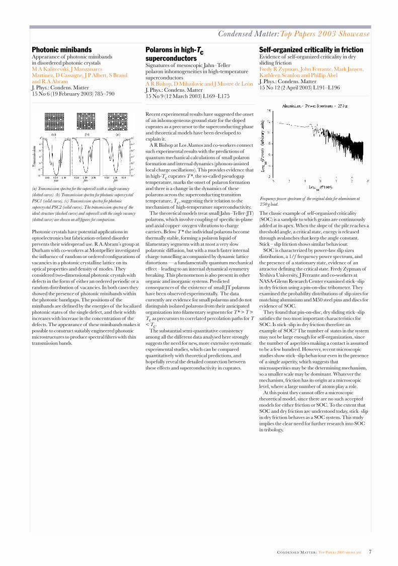
‘Hot’ spin iceDynamical crossover in 'hot' spin iceG Ehlers, A L Cornelius, M Orendác,M Kajnaková, T Fennell, S T Bramwell and J S GardnerJ. Phys.: Condens. Matter 15 No 2 (22 January 2003) L9–L15
In materials such as LiHoF4, in which the spin isconfined to a double-well potential of depth D arisingfrom the crystalline electric field, quasiclassical spinreorientations are precluded at temperatures T �D/kB, but spin relaxation may still occur. Directtransitions of this sort, between degenerate |±MJ�states on either side of the barrier, are referred to as‘spin tunnelling’.
In the ‘spin ice’ materials Ho2Ti2O2, Dy2Ti2O7,and Ho2Sn2O7, D/kB > 200 K is much larger thanin other magnets. The spins are constrained to localaxes, which leads to frozen, non-collinear, spindisorder below ~1K.
S T Bramwell of University College London,J S Gardner at NIST and co-workers have isolatedthe spectral properties of spin-ice materials and,where possible, identified their origin using theelegant technique of neutron spin echo, whichinvolves a beam of spin-polarized neutrons executinga fixed number (say N ) of spin precessions prior tostriking the sample. The sense of the precession isthen reversed by static magnetic fields near to thesample position. After N further precessions theoriginal polarization is restored, unless scatteringprocesses in the sample have produced a phase shift.
In conclusion, Ho2Ti2O7 presents a very differentscenario to other quantum magnets, as here thetunnelling dynamics are an intrinsic consequence ofthe geometric frustration that prevents magneticordering. Cooperative quantum tunnelling occursover a broad range of unusually high temperatures,from T ≈ 1–15 K, while a single-ion processdominates above 15 K. The authors have elucidatedthe main relaxation processes in the ‘hot’paramagnetic phase of Ho2Ti2O7 and the otherspin ices, which they believe may represent aremarkable new class of quantum dynamicalmagnet.
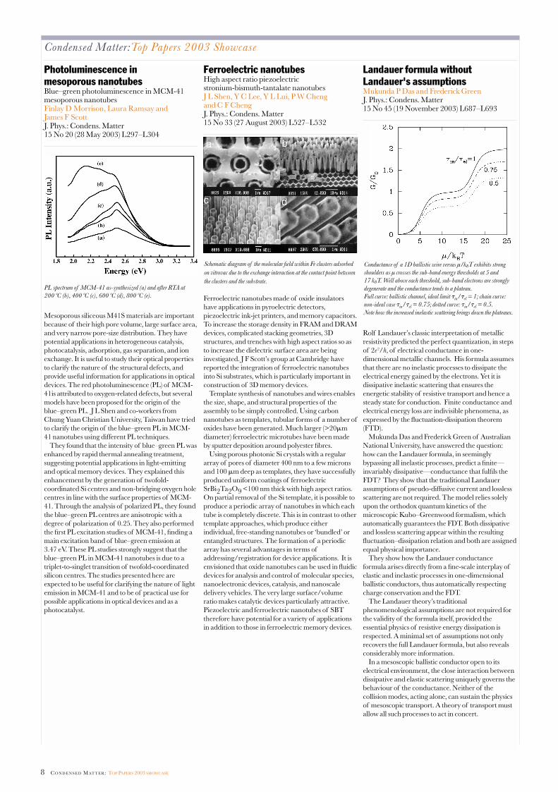
Magnetism of metal clustersOn the oscillation of the magnetic moment of free transition metal clustersYuannan Xie and John A BlackmanJ. Phys.: Condens. Matter 15 No 40 (15 October 2003) L615–L622
A better understanding of magnetism in transitionmetal clusters is crucial not only for fundamentalphysics but also for potential applications in high-density data storage devices.
The results of Stern–Gerlach experiments on freeclusters of Fe, Co, and Ni are usually interpreted interms of magnetic moments that show oscillations asa function of cluster size. Yuannan Xie and JohnBlackman of Reading have shown that the observedbehaviour can be more convincingly explained interms of magnetic anisotropy energies (MAEs) thatoscillate with the size of the clusters.
The MAE, i.e. the energy involved in rotating themagnetization from a low energy direction (easy axis)to a high energy direction (hard axis), determines thelow temperature orientation of the magnetizationwith respect to the structure of the system. TheMAEs of clusters are higher than the bulk valuesbecause of a strong anisotropy induced at the surfaceof the clusters.
They show that the apparent oscillations of themagnetic moments present in the experiments on freeclusters can be properly analysed by taking the MAEinto account. The MAEs of free Fe, Co, and Niclusters are estimated under various reasonableexperimental conditions and theoretical postulates.The estimated MAEs are in reasonably goodagreement with the experimental results forsupported/embedded cluster assemblies, whichverifies the validity of their theoretical model.
Condensed Matter:Top Papers 2003 Showcase
The dispersion curve for liquid 4He showing the phonon, R - roton and
R+roton regions.
AC susceptibility results for Ho2 Ti2 O7, measured with a field of
I T along [111], revealing a peak ~ 15 K. Inset shows an Arrhenius
plot for the frequency shift of the ~ 1 K peak in polycrystalline
Ho2 Ti2 O2 (squares) and Ho1.9 La0.1 Ti2 O7 (circles) showing
how doping increases the attempt frequency for the lower temperature
process.
Total average magnetic moments � tot and MAEs calculated
fromTB models for (a) Co201 and (b) Co209. Co209 is constructed
from Co201 by adding one layer (shadowed atoms) to the top and
bottom squares.
CO N D E N S E D MAT T E R: TOP PAPERS 2003 SHOWCASE 7
Photonic minibands Appearance of photonic minibands in disordered photonic crystalsM A Kaliteevski, J Manzanares Martinez, D Cassagne, J P Albert, S Brand and R A AbramJ. Phys.: Condens. Matter 15 No 6 (19 February 2003) 785–790
Photonic crystals have potential applications inoptoelectronics but fabrication-related disorderprevents their widespread use. R A Abram’s group atDurham with co-workers at Montpellier investigatedthe influence of random or ordered configurations ofvacancies in a photonic crystalline lattice on itsoptical properties and density of modes. Theyconsidered two-dimensional photonic crystals withdefects in the form of either an ordered periodic or arandom distribution of vacancies. In both cases theyshowed the presence of photonic minibands withinthe photonic bandgaps. The positions of theminibands are defined by the energies of the localizedphotonic states of the single defect, and their widthincreases with increase in the concentration of thedefects. The appearance of these minibands makes itpossible to construct suitably engineered photonicmicrostructures to produce spectral filters with thintransmission bands.
Polarons in high-TcsuperconductorsSignatures of mesoscopic Jahn–Teller polaron inhomogeneities in high-temperaturesuperconductorsA R Bishop, D Mihailovic and J Mustre de LeónJ. Phys.: Condens. Matter 15 No 9 (12 March 2003) L169–L175
Recent experimental results have suggested the onsetof an inhomogeneous ground state for the dopedcuprates as a precursor to the superconducting phaseand theoretical models have been developed toexplain it.
A R Bishop at Los Alamos and co-workers connectsuch experimental results with the predictions ofquantum mechanical calculations of small polaronformation and internal dynamics (phonon-assistedlocal charge oscillations). This provides evidence thatin high-Tc cuprates T *, the so-called pseudogaptemperature, marks the onset of polaron formationand there is a change in the dynamics of thesepolarons across the superconducting transitiontemperature, Tc, suggesting their relation to themechanism of high-temperature superconductivity.
The theoretical models treat small Jahn–Teller (JT)polarons, which involve coupling of specific in-planeand axial copper–oxygen vibrations to chargecarriers. Below T * the individual polarons becomethermally stable, forming a polaron liquid offilamentary segments with at most a very slowpolaronic diffusion, but with a much faster internalcharge tunnelling accompanied by dynamic latticedistortions — a fundamentally quantum mechanicaleffect – leading to an internal dynamical symmetrybreaking. This phenomenon is also present in otherorganic and inorganic systems. Predictedconsequences of the existence of small JT polaronshave been observed experimentally. The datacurrently are evidence for small polarons and do notdistinguish isolated polarons from their anticipatedorganization into filamentary segments for T * > T >Tc as precursors to correlated percolation paths for T< Tc.
The substantial semi-quantitative consistencyamong all the different data analysed here stronglysuggests the need for new, more extensive systematicexperimental studies, which can be comparedquantitatively with theoretical predictions, andhopefully reveal the detailed connection betweenthese effects and superconductivity in cuprates.
Self-organized criticality in frictionEvidence of self-organized criticality in dry sliding frictionFredy R Zypman, John Ferrante, Mark Jansen,Kathleen Scanlon and Phillip AbelJ. Phys.: Condens. Matter 15 No 12 (2 April 2003) L191–L196
The classic example of self-organized criticality(SOC) is a sandpile to which grains are continuouslyadded at its apex. When the slope of the pile reaches athreshold angle, a critical state, energy is releasedthrough avalanches that keep the angle constant.Stick – slip friction shows similar behaviour.
SOC is characterized by power-law slip sizesdistribution, a 1/f frequency power spectrum, andthe presence of a stationary state, evidence of anattractor defining the critical state. Fredy Zypman ofYeshiva University, J Ferrante and co-workers atNASA-Glenn Research Center examined stick–slipin dry friction using a pin-on-disc tribometer. Theyexamined the probability distributions of slip sizes formatching aluminium and M50 steel pins and discs forevidence of SOC.
They found that pin-on-disc, dry sliding stick–slipsatisfies the two most important characteristics forSOC. Is stick–slip in dry friction therefore anexample of SOC? The number of states in the systemmay not be large enough for self-organization, sincethe number of asperities making a contact is assumedto be a few hundred. However, recent microscopicstudies show stick–slip behaviour even in the presenceof a single asperity, which suggests thatmicroasperities may be the determining mechanism,so a smaller scale may be dominant. Whatever themechanism, friction has its origin at a microscopiclevel, where a large number of atoms play a role.
At this point they cannot offer a microscopictheoretical model, since there are no such acceptedmodels for either friction or SOC. To the extent thatSOC and dry friction are understood today, stick–slipin dry friction behaves as a SOC system. This studyimplies the clear need for further research into SOCin tribology.
Condensed Matter:Top Papers 2003 Showcase
(a) Transmission spectra for the supercell with a single vacancy
(dotted curve). (b) Transmission spectra for photonic supercrystal
PSC1 (solid curve). (c) Transmission spectra for photonic
supercrystal PSC2 (solid curve). The transmission spectra of the
ideal structure (dashed curve) and supercell with the single vacancy
(dotted curve) are shown on all figures for comparison.
Frequency power spectrum of the original data for aluminium at
250 g load.
8 CO N D E N S E D MAT T E R: TOP PAPERS 2003 SHOWCASE
Photoluminescence in mesoporous nanotubesBlue–green photoluminescence in MCM-41mesoporous nanotubesFinlay D Morrison, Laura Ramsay and James F ScottJ. Phys.: Condens. Matter 15 No 20 (28 May 2003) L297–L304
Mesoporous siliceous M41S materials are importantbecause of their high pore volume, large surface area,and very narrow pore-size distribution. They havepotential applications in heterogeneous catalysis,photocatalysis, adsorption, gas separation, and ionexchange. It is useful to study their optical propertiesto clarify the nature of the structural defects, andprovide useful information for applications in opticaldevices. The red photoluminescence (PL) of MCM-41is attributed to oxygen-related defects, but severalmodels have been proposed for the origin of theblue–green PL. J L Shen and co-workers fromChung Yuan Christian University, Taiwan have triedto clarify the origin of the blue–green PL in MCM-41 nanotubes using different PL techniques.
They found that the intensity of blue–green PL wasenhanced by rapid thermal annealing treatment,suggesting potential applications in light-emittingand optical memory devices. They explained thisenhancement by the generation of twofold-coordinated Si centres and non-bridging oxygen holecentres in line with the surface properties of MCM-41. Through the analysis of polarized PL, they foundthe blue–green PL centres are anisotropic with adegree of polarization of 0.25. They also performedthe first PL excitation studies of MCM-41, finding amain excitation band of blue–green emission at 3.47 eV. These PL studies strongly suggest that theblue–green PL in MCM-41 nanotubes is due to atriplet-to-singlet transition of twofold-coordinatedsilicon centres. The studies presented here areexpected to be useful for clarifying the nature of lightemission in MCM-41 and to be of practical use forpossible applications in optical devices and as aphotocatalyst.
Ferroelectric nanotubesHigh aspect ratio piezoelectric stronium-bismuth-tantalate nanotubesJ L Shen, Y C Lee, Y L Lui, P W Cheng and C F ChengJ. Phys.: Condens. Matter 15 No 33 (27 August 2003) L527–L532
Ferroelectric nanotubes made of oxide insulatorshave applications in pyroelectric detectors,piezoelectric ink-jet printers, and memory capacitors.To increase the storage density in FRAM and DRAMdevices, complicated stacking geometries, 3Dstructures, and trenches with high aspect ratios so asto increase the dielectric surface area are beinginvestigated. J F Scott’s group at Cambridge havereported the integration of ferroelectric nanotubesinto Si substrates, which is particularly important inconstruction of 3D memory devices.
Template synthesis of nanotubes and wires enablesthe size, shape, and structural properties of theassembly to be simply controlled. Using carbonnanotubes as templates, tubular forms of a number ofoxides have been generated. Much larger (>20�mdiameter) ferroelectric microtubes have been madeby sputter deposition around polyester fibres.
Using porous photonic Si crystals with a regulararray of pores of diameter 400 nm to a few micronsand 100 �m deep as templates, they have successfullyproduced uniform coatings of ferroelectricSrBi2Ta2O9 <100 nm thick with high aspect ratios.On partial removal of the Si template, it is possible toproduce a periodic array of nanotubes in which eachtube is completely discrete. This is in contrast to othertemplate approaches, which produce eitherindividual, free-standing nanotubes or ‘bundled’ orentangled structures. The formation of a periodicarray has several advantages in terms ofaddressing/registration for device applications. It isenvisioned that oxide nanotubes can be used in fluidicdevices for analysis and control of molecular species,nanoelectronic devices, catalysis, and nanoscaledelivery vehicles. The very large surface/volumeratio makes catalytic devices particularly attractive.Piezoelectric and ferroelectric nanotubes of SBTtherefore have potential for a variety of applicationsin addition to those in ferroelectric memory devices.
Landauer formula withoutLandauer's assumptionsMukunda P Das and Frederick GreenJ. Phys.: Condens. Matter 15 No 45 (19 November 2003) L687–L693
Rolf Landauer’s classic interpretation of metallicresistivity predicted the perfect quantization, in stepsof 2e 2/h, of electrical conductance in one-dimensional metallic channels. His formula assumesthat there are no inelastic processes to dissipate theelectrical energy gained by the electrons. Yet it isdissipative inelastic scattering that ensures theenergetic stability of resistive transport and hence asteady state for conduction. Finite conductance andelectrical energy loss are indivisible phenomena, asexpressed by the fluctuation-dissipation theorem(FTD).
Mukunda Das and Frederick Green of AustralianNational University, have answered the question:how can the Landauer formula, in seeminglybypassing all inelastic processes, predict a finite—invariably dissipative—conductance that fulfils theFDT? They show that the traditional Landauerassumptions of pseudo-diffusive current and losslessscattering are not required. The model relies solelyupon the orthodox quantum kinetics of themicroscopic Kubo–Greenwood formalism, whichautomatically guarantees the FDT. Both dissipativeand lossless scattering appear within the resultingfluctuation–dissipation relation and both are assignedequal physical importance.
They show how the Landauer conductanceformula arises directly from a fine-scale interplay ofelastic and inelastic processes in one-dimensionalballistic conductors, thus automatically respectingcharge conservation and the FDT.
The Landauer theory’s traditionalphenomenological assumptions are not required forthe validity of the formula itself, provided theessential physics of resistive energy dissipation isrespected. A minimal set of assumptions not onlyrecovers the full Landauer formula, but also revealsconsiderably more information.
In a mesoscopic ballistic conductor open to itselectrical environment, the close interaction betweendissipative and elastic scattering uniquely governs thebehaviour of the conductance. Neither of thecollision modes, acting alone, can sustain the physicsof mesoscopic transport. A theory of transport mustallow all such processes to act in concert.
Condensed Matter:Top Papers 2003 Showcase
Schematic diagram of the molecular field within Fe clusters adsorbed
on vitrovac due to the exchange interaction at the contact point between
the clusters and the substrate.PL spectrum of MCM-41 as-synthesized (a) and after RTA at
200 ºC (b), 400 ºC (c), 600 ºC (d), 800 ºC (e).
Conductance of a 1D ballistic wire versus µ/kBT exhibits strong
shoulders as µ crosses the sub-band energy thresholds at 5 and
17 kBT. Well above each threshold, sub-band electrons are strongly
degenerate and the conductance tends to a plateau.
Full curve: ballistic channel, ideal limit �in/�el = 1; chain curve:
non-ideal case �in/�el = 0.75; dotted curve: �in/�el = 0.5.
Note how the increased inelastic scattering brings down the plateaux.

CO N D E N S E D MAT T E R: TOP PAPERS 2003 SHOWCASE 9
Encapsulated magnetite particlesfor biomedical applicationKatharina Landfester and Liliana P RamírezJ. Phys.: Condens. Matter 15 No 15 (23 April 2003) S1345–S1361
Particles composed of polymers or hybrid polymericand magnetic materials have important biomedicalapplications, for which they need to be biocompatibleand non-toxic, and sometimes also biodegradable.Many different approaches are used to producenanoparticles with these properties.
Katharina Landfester and Liliana P Ramírez ofMPI of Colloids and Interfaces, Potsdam, havedemonstrated the possibility of using theminiemulsion process for formulation of magneticnanoparticles. The encapsulation of large numbersof magnetite particles into polystyrene particles canbe achieved efficiently by a new three-steppreparation route including two miniemulsionprocesses. First, oleic-acid-coated magnetite particlesin octane are prepared. Secondly, a dispersion of themagnetite in octane is miniemulsified in water byusing SDS as the surfactant. After evaporation of theoctane, the magnetite aggregates which are coveredby an oleic acid/SDS bilayer are mixed with amonomer miniemulsion and, in the third step, an ad-miniemulsification process is used to obtain final andfull encapsulation. Here, a fusion/fission processinduced by ultrasound is only effective for themonomer droplets, whereas the monomer-coatedmagnetite aggregates remain intact. In that way, allmonomer droplets are split and heteronucleated ontothe magnetite aggregates to form a monomer film.After polymerization, polymer-encapsulatedmagnetite aggregates were obtained.Characterization by thermogravimetry, preparativeultracentrifugation and transmission electronmicroscopy showed that up to 40% magnetite couldbe encapsulated, resulting in particles with a highhomogeneity of the magnetite content.
Magnetometry measurements reveal that themagnetite aggregates still consist of separatedsuperparamagnetic magnetite particles, which is dueto the coverage by the oleic acid. During theencapsulation process, 60% of the magnetizationcompared to bulk magnetite is preserved.
Self-trapped states in proteins?Robert H Austin, Aihua Xie, Lex van der Meer,Michelle Shinn and George NeilJ. Phys.: Condens. Matter 15 No 18 (14 May 2003) S1693–S1698
Energy and charge transport are crucial to life. Howcan the energy from light or chemical processes bemoved around and used efficiently at normaltemperatures? In the 1970s, Davydov suggested thatsolitons provided an effective mechanism for energytransfer in proteins. Verifying this has proved difficult,for it is hard to identify a ‘smoking gun’ to be sure ofan identification.
Robert Austin (Princeton) and his co-workers havefound that experiments exploiting the short, turnablepulses from free-electron lasers appear to resolvesome of the key questions. The temperaturedependence of the amide I band of myoglobin showsevidence for a low-lying self-trapped state at 6.15�m.Careful picosecond pump-probe experiments as afunction of temperature and wavelength show thatthis low-lying state has a 30 ps lifetime at 50 K, muchlonger than the relaxation time of the main amide Iband at 50 K. A fit of the temperature dependenceindicates that it lies 280 K below the main amide Iband.
Since the gap energy of this state is of the order ofroom temperature, this self-trapped state can act as atransient store of vibrational energy at physiologicaltemperatures in biomolecules, and can help to directthe path of energy flow in a biomolecule underbiological conditions.
A new superconductorSuperconductivity in a pyrochlore-related oxide KOs2O6S Yonezawa, Y Muraoka, Y Matsushita and Z HiroiJ. Phys.: Condens. Matter 16 No 3 (28 January 2004) L9-L12
Pyrochlore oxides have a general chemical formulaA2B2O7 or A2B2O6', where A is a larger cation andB is a smaller transition metal (TM) cation. Mostpyrochlore oxides containing 5d TM elements suchas Re, Os and Ir are bad metals. Recently,superconductivity was found for the first time in apyrochlore oxide in Cd2Re2O7 at Tc = 1 K. Arelated pyrochlore oxide Cd2Os2O7 undergoes ametal–insulator (MI) transition at 225 K. The majordifference between them seems to be the number of delectrons on the B-site cations: Re5+ being 5d2 andOs5+ 5d3.
S Yonezawa’s group from Tokyo have reported thediscovery of superconductivity in a new ternaryphase KOs2O6. Polycrystalline samples wereprepared from KO2 and OsO2 powders. Resistivitymeasurements showed a superconducting transitionwith onset temperature 9.9 K and zero resistivitybelow 9.0 K. When a magnetic field was applied, thetransition curve shifted to lower temperaturessystematically. The resistivity above the transitionshows a peculiar temperature dependence, which isfar from that of a conventional metal. Measurementson a single crystal instead of a polycrystalline pelletare needed to clarify this point. The sample alsoshowed a Meissner effect below 9.6 K. Thesuperconducting volume fraction estimated at 2 Kfrom the zero-field cooling experiment is about 80%,which is large enough to constitute bulksuperconductivity.
They believe that an interesting physical process isinvolved in this compound on the basis of electroncorrelations near the MI transition as well asfrustration on the pyrochlore lattice
Condensed Matter:Top Papers 2003 Showcase
Probable crystal structure for KOs2O6. K, Os and O atoms occupy
the 8b, 16c and 48f sites in the space group Fd ̄3m, respectively.
TEM images for magnetite polystyrene particles at different
magnifications.
Temperature dependence of sperm whale MB (swMB) in the region
1800–1400 cm-1. The colours of the curves are spectrally coded to
correspond to temperature, with red = 300 K, yellow = 180 K and
blue = 5 K.
Difference spectra taken from the figure above, using the same colour
scheme to plot difference between absorbance at temperature T and at
300 K.
10 CO N D E N S E D MAT T E R: TOP PAPERS 2003 SHOWCASE
MesomagnetismThe defining length scales of mesomagnetism:a reviewC L Dennis, R P Borges, L D Buda, U Ebels,J F Gregg, M Hehn, E Jouguelet, K Ounadjela,I Petej, I L Prejbeanu and M J ThorntonJ. Phys.: Condens. Matter14 No 49 (16 December 2002) R1175–R1262
Mesomagnetism is the study of the novel physicalphenomena which appear when magnetic systemsare reduced to the nanoscale. Magnetic processes arecharacterized by specific length scales and when thephysical size of a magnetic system is engineered tothese or smaller dimensions, novel behaviour isobserved. Examples include giant magnetoresistance(GMR), Coulomb blockade, perpendicularanisotropy, superparamagnetism and current-induced switching.
As technology continues to miniaturize and novelmaterials are developed, these characteristic lengthscales and their resulting phenomena define theultimate limits of devices. Many of these mesoscopiccharacteristic length scales— domain size, domainwall width, exchange length and thin filmperpendicular anisotropy threshold—are governedby minimization of energy considerations. Others,like the spin diffusion length and spin precessionlength, are the result of diffusion processes for energy,momentum or magnetization. The phenomena thatappear when magnetic systems are engineered onthese length scales may be very diverse since a widevariety of combinations of several characteristiclengths may be involved.
These mesoscopic phenomena place ultimate limitson device performance, improve current technologyor generate new technology. The electronics, datastorage and computer industries and other industriesincluding medical technology are continuouslypushing the limits of technology. This has led to thedevelopment of novel devices (such as biologicalphysics sensors for medicine) as well as advancementsin GMR for read heads in data storage, theinvestigations into domains in granular media fordata storage, magnetic field sensing for automotivesensors (and other applications which requiresensors), MRAM and many others. Otherinvestigations are pursuing more advanced conceptslike single electronics for quantum computers.
A review by J F Gregg’s group at Oxford and co-workers at IPCMS, Strasbourg, and Université HenriPoincaré, Nancy provides an introduction tomesomagnetism, exploring the connections betweenthe different phenomena and their characteristiclength scales as well as their relevance to (or operationin) devices.
Organic electronicsOrganic–inorganic semiconductor devices and3, 4, 9, 10 perylenetetracarboxylic dianhydride:an early history of organic electronicsS R Forrest J. Phys.: Condens. Matter15 No 38 (1 October 2003) S2599-S2610
The first organic-on-inorganic semiconductorheterojunction (OI HJ) was demonstrated in 1981,with the organic semiconductor 3, 4, 9, 10perylenetetracarboxylic dianhydride (PTCDA), i.e.C24O6H8.
S R Forrest of Princeton first investigated a teststructure consisting of a metal contact and a 100–500nm thick layer of PTCDA on a p-type Si substrate. Itwas expected to result in a simple metal–insulator–Sicapacitor but, surprisingly, PTCDA formed arectifying contact on Si, with nearly idealcharacteristics. Both n- and p-type substrates, notonly of Si but also of such materials as GaAs and InP,formed rectifying junctions with an organicsemiconductor layer.
Forrest reviews possible applications of organic-inorganic heterojunction devices and describes thedramatic change in conductive properties of thesematerials when exposed to high-energy ion beams.
The prospects for hybrid organic-on-inorganicsemiconductor structures for use in electronic andphotonic applications are also presented, whichinclude non-linear optical elements and evenmemory devices. While it remains to be seen whichapplications will emerge, the rapidly growing interestin organic electronics will almost certainly open aniche for OI HJ devices based on their very highperformance and simplicity of fabrication.
Moreover, the extensive study of the remarkable,archetypal compound PTCDA has revealed muchfundamental knowledge in the physics of organicsemiconductors in general. Controlled OMBDgrowth has led to unprecedented film quality, whichhas allowed exploration of the spectroscopic andconductive properties of this material in films withordered structures and of thicknesses from sub-monolayer to several microns. Analogues of PTCDAare showing promise for use in transistors, organicsolar cells and photodetectors. Thus, the lessonslearnt from this remarkable organic semiconductorwill stimulate further rapid advances in organicelectronics.
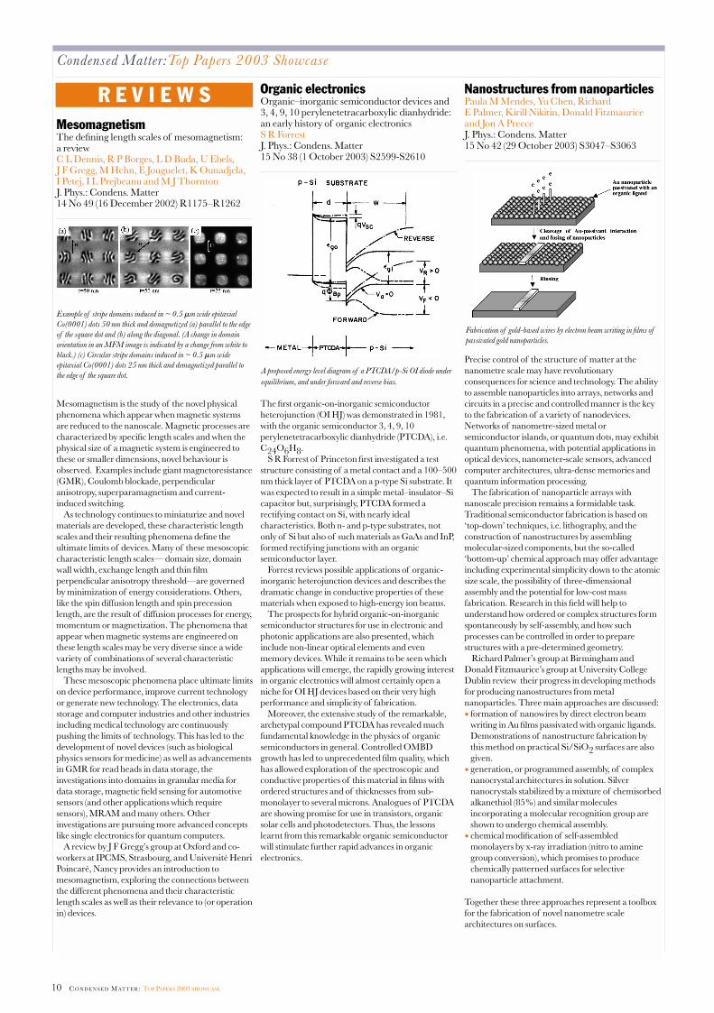
Nanostructures from nanoparticlesPaula M Mendes, Yu Chen, Richard E Palmer, Kirill Nikitin, Donald Fitzmauriceand Jon A PreeceJ. Phys.: Condens. Matter15 No 42 (29 October 2003) S3047–S3063
Precise control of the structure of matter at thenanometre scale may have revolutionaryconsequences for science and technology. The abilityto assemble nanoparticles into arrays, networks andcircuits in a precise and controlled manner is the keyto the fabrication of a variety of nanodevices.Networks of nanometre-sized metal orsemiconductor islands, or quantum dots, may exhibitquantum phenomena, with potential applications inoptical devices, nanometer-scale sensors, advancedcomputer architectures, ultra-dense memories andquantum information processing.
The fabrication of nanoparticle arrays withnanoscale precision remains a formidable task.Traditional semiconductor fabrication is based on‘top-down’ techniques, i.e. lithography, and theconstruction of nanostructures by assemblingmolecular-sized components, but the so-called‘bottom-up’ chemical approach may offer advantageincluding experimental simplicity down to the atomicsize scale, the possibility of three-dimensionalassembly and the potential for low-cost massfabrication. Research in this field will help tounderstand how ordered or complex structures formspontaneously by self-assembly, and how suchprocesses can be controlled in order to preparestructures with a pre-determined geometry.
Richard Palmer’s group at Birmingham andDonald Fitzmaurice’s group at University CollegeDublin review their progress in developing methodsfor producing nanostructures from metalnanoparticles. Three main approaches are discussed:• formation of nanowires by direct electron beam
writing in Au films passivated with organic ligands.Demonstrations of nanostructure fabrication bythis method on practical Si/SiO2 surfaces are alsogiven.
• generation, or programmed assembly, of complexnanocrystal architectures in solution. Silvernanocrystals stabilized by a mixture of chemisorbedalkanethiol (85%) and similar moleculesincorporating a molecular recognition group areshown to undergo chemical assembly.
• chemical modification of self-assembledmonolayers by x-ray irradiation (nitro to aminegroup conversion), which promises to producechemically patterned surfaces for selectivenanoparticle attachment.
Together these three approaches represent a toolboxfor the fabrication of novel nanometre scalearchitectures on surfaces.
Condensed Matter:Top Papers 2003 Showcase
R E V I E W S
A proposed energy level diagram of a PTCDA/p-Si OI diode under
equilibrium, and under forward and reverse bias.
Fabrication of gold-based wires by electron beam writing in films of
passivated gold nanoparticles.
Example of stripe domains induced in ~ 0.5 �m wide epitaxial
Co(0001) dots 50 nm thick and demagnetized (a) parallel to the edge
of the square dot and (b) along the diagonal. (A change in domain
orientation in an MFM image is indicated by a change from white to
black.) (c) Circular stripe domains induced in ~ 0.5 �m wide
epitaxial Co(0001) dots 25 nm thick and demagnetized parallel to
the edge of the square dot.

CO N D E N S E D MAT T E R: TOP PAPERS 2003 SHOWCASE 11
Magnetism of films, stripes and dotsThe effect of spatial confinement on magnetism:films, stripes and dots of Fe on Cu(111)J Shen et al.J. Phys.: Condens. Matter 15 No 2 (22 January 2003) R1-R30
Magnetic nanostructures are important both for theirbasic physics and device applications. Newproperties that emerge at the nanoscale have at leastfour origins:
(1) Surface and interface effects dominate as thesurface-to-volume ratio increases.
(2) New quantum phenomena such as oscillatoryexchange coupling, GMR, spin-dependenttunnelling and exchange bias manifest in magneticmultilayers.
(3) Effects when the system dimensions arecomparable with ‘characteristic lengths’ such as thespin-diffusion length — the exotic effects seen inGMR spin valves, for example.
(4) In many spin systems, like CMR materials andmagnetic semiconductors, correlation effects spinfluctuations and spin transport, already important inthe bulk spin structure, are enhanced by spatialconfinement.
E W Plummer’s group at Oak Ridge and JKirschner at MPI for Microstructure physics, Hallereview the successful growth of ultrathin films,nanowires and nanodots of Fe on Cu(111) using self-assembly principles, even though they cannot begrown by conventional techniques. The fact thatthese three types of nanostructures can be grown on acommon template allows direct observation of theeffects when the Fe nanostructures are smaller thanthe magnetic domain size in one, two and threedimensions. This particular system, Fe on Cu(111),has shown that the magnetic properties of a systemdo not change monotonically and predictably as thedimensionality of the system is reduced. Unresolvedissues include the microscopic origin of the low-moment phase and the anomalous thicknessdependence of the Curie temperature in laser MBE-grown films, and the surprising difference in themagnetic stability of the nanowire and quantumsystems.
Future work on magnetic nanostructures preparedon insulating substrates, where there would be trueconfinement of the electrons, could be of particularimportance. These systems might show, for instance,how electron spin can influence electronic transportin a magnetic nanowire. However, a considerableamount of work remains in developing techniques forthe controlled synthesis of such systems.
Spin-dependent tunnellingSpin-dependent tunnelling in magnetic tunneljunctionsEvgeny Y Tsymbal, Oleg N Mryasov and Patrick R LeClairJ. Phys.: Condens. Matter 15 No 4 (5 February 2003) R109–R142
A magnetic tunnel junction (MTJ) consists of twoferromagnetic metal films separated by an insulatingbarrier layer. The insulating layer is so thin (a fewnanometres or less) that electrons can tunnel throughthe barrier if a bias voltage is applied. The tunnellingcurrent depends on the relative orientation of themagnetizations of the two ferromagnetic films, whichcan be changed by an applied magnetic field — so-called tunnelling magnetoresistance (TMR).
MTJs based on 3d-metal ferromagnets and Al2O3barriers can now be fabricated with reproduciblecharacteristics and with TMR values up to 50% atroom temperature, making them suitable forindustrial applications. TMR is a consequence ofspin-dependent tunnelling, which is an imbalance inthe electric current carried by up- and down-spinelectrons. The tunnelling spin polarization is not anintrinsic property of the ferromagnet alone butdepends on the structural and electronic properties ofthe entire junction. This makes the quantitativedescription of transport characteristics of MTJsmuch more complicated, but broadens thepossibilities for engineering the properties of MTJsfor device applications. The various factors thatcontrol the magnitude of TMR in MTJs have beenreviewed by Evgeny Tsymbal of University ofNebraska-Lincoln and co-workers.
Atom lithography One-, two-and three-dimensionalnanostructures with atom lithographyMarkus K Oberthaler and Tilman PfauJ. Phys.: Condens. Matter 15 No 6 (19 February 2003) R233-R255
The semiconductor industry is still based on opticallithography using light with a wavelength of 157 nm,which limits feature widths to about 100 nm.Alternative lithography techniques, like electron-beam, ion-beam and x-ray lithography can producenanostructures with a resolution of a few nm. Newtechniques of nanostructures production are beingdeveloped including scanning probe techniques,imprint techniques, self-assembly of structures andatom lithography.
Markus Oberthaler of Konstanz and Tilman Pfauof Stuttgart review the current status in the field ofatom lithography. In atom lithography, conversely tolight lithography, light acts as a mask and atoms formthe pattern. The nanostructures on the surface of asubstrate are either formed by the deposited atomsthemselves or, in close analogy to photolithography,by using a special resist, sensitive to the atomic beam,and successive etching steps. Since atoms, whose deBroglie wavelength is only a few pm, are imaged ontothe surface, diffraction effects are currently not alimiting factor. It discusses in detail how atom–lightinteraction allows masks for atoms to be formed andthe possible nanostructures and limitations of thismethod.
One-, two- and three-dimensional structures havebeen produced. The straightforward extension tothree-dimensional structuring is a particular strengthof this method. Another strength is the possibility ofproducing long-range (up to mm2) ordered periodicnanostructures with a feature size of 30 nm andperiod of 213 nm in the case of chromium.
In future this method will be extended totechnologically interesting atomic species such asgroup III atoms, and combined with epitaxialgrowth. The successful combination of the field ofepitaxial growth and atom optics will open up theway for producing new nanostructured materialswith new properties.
Condensed Matter:Top Papers 2003 Showcase
Two types of light masks employed in atom lithography experiments.
A well collimated atomic beam impinges onto a light field. A light force
mask can be described by a harmonic potential which acts like a lens
for matter waves, leading to a locally enhanced growth rate on the
substrate. In the case of an absorptive mask no force is present but
atoms in the metastable state are pumped to the ground state except at a
position where the intensity is very small. Combining this with a resist
which is only sensitive to metastable atoms, due to their high internal
energy, allows us to transfer this pattern onto a substrate.
Schematics showing the phenomenon of twinning. The spacing
between iron atoms on the Cu(111) surface is such that iron atoms in
a particular island will either occupy ‘A’ sites only or ‘B’ sites only,
depending on which of these two sites was settled upon by the atom
that seeded the island. The image shows the fault line that forms when
an A-type island tries to merge with a B-type island.
The first observation of reproducible, large room temperature
magnetoresistance in a CoFe/Al2O3/Co MTJ. The arrows indicate
the relative magnetization orientation in the CoFe and Co layers.
The calculated atomic structure and local DOS for majority-spin
electrons (top panels) and minority-spin electrons (bottom panels) for
a Co/Al2O3/Co tunnel junction.

12 CO N D E N S E D MAT T E R: TOP PAPERS 2003 SHOWCASE
Relaxor ferroelectricsThe relaxational properties of compositionallydisordered ABO3 perovskitesGeorge A SamaraJ. Phys.: Condens. Matter 15 No 9 (12 March 2003) R367-R411
The ABO3 perovskite oxides have helped ourunderstanding of ferroelectric and antiferroelectricphenomena. They are prototypical soft phononmode systems that undergo structural phasetransitions involving both polar and non-polardistortions of the cubic lattice.
Random lattice disorder produced by chemicalsubstitution can lead to the formation of dipolarimpurities and defects that have a profound influenceon their static and dynamic properties. In these highlypolarizable host lattices, dipolar entities form polarnanodomains whose size is determined by the dipolarcorrelation length, rc, of the host and that exhibitdielectric relaxation in an applied ac field. In the verydilute limit (<0.1 at.%) each domain behaves as anon-interacting dipolar entity with a single relaxationtime. At higher concentrations of disorder thedomains can interact leading to more complexrelaxational behaviour, including the formation of aglass-like relaxor state, or even an orderedferroelectric state for a sufficiently high concentrationof overlapping domains.
George Samara of Sandia National Laboratoriesreviews these materials, beginning with the simplestcases, namely the relaxational properties ofsubstitutional impurities (e.g., Mn, Fe and Ca) in thequantum paraelectrics KTaO3 and SrTiO3,followed by discussions of the relaxational propertiesof Li- and Nb-doped KTaO3 and of the strongrelaxors in the PbMg1/3Nb2/3O3 and La-substituted PbZr1-xTixO3 families. He discussesthe roles of pressure and applied dc biasing electricfields in understanding the physics of these materialsincluding the relaxor-to-ferroelectric crossover.
Relaxors have been one of the ‘hot’ topics inferroelectricity during the recent past. Theexceptionally large dielectric susceptibilities,electromechanical coupling coefficients and electro-optic constants of perovskite relaxors have beensubjects of intense scientific and technologicalinterest. The scientific challenges and technologicalpotential of these materials will ensure that this fieldwill continue to be quite active for the foreseeablefuture.
NanomagneticsR SkomskiJ. Phys.: Condens. Matter 15 No 20 (28 May 2003) R841–R896
R Skomski of University of Nebraska, Lincolnreviews magnetic nanostructures, such as dots anddot arrays, nanowires, multilayers and nanojunctionsand compares them with bulk magnets. Theemphasis is on the physics, but some applications arealso outlined, including permanent magnets, softmagnets, magnetic recording media, sensors, andstructures and materials for spin electronics. Theconsidered structural length scales range from a fewinteratomic distances to about one micrometre,bridging the gap between atomic-scale magnetismand the macroscopic magnetism of extended bulkand thin-film magnets. This leads to a rich variety ofphysical phenomena, including exchange-springmagnetism, random-anisotropy scaling, narrow-walland constricted-wall phenomena, Curie temperaturechanges due to nanostructuring and nanoscalemagnetization dynamics.
The search for materials with improved intrinsicproperties continues to be of scientific andtechnological interest, but a main thrust of research isthe exploitation of artificial nanostructures, yieldingmaterials and functional components not found innature. An end to the search for new geometries andmicrochemistries is not yet in sight, and fully realizingthe range of magnetic nanostructures and theirpotential for exploring new applications remains achallenge for future research. The technologicalprogress is accompanied and stimulated by an ever-improving understanding of the magnetic propertiesof nanostructures. For example, we now understandthe crucial effect of imperfections, which largelydetermine the hysteresis loop and the real-spacerealization of magnetization processes. In addition tomodel calculations, full-scale simulations of realstructures are now on the horizon, and sophisticatedexperimental investigation and processing techniqueswill ensure far-reaching qualitative and quantitativedevelopments.
Publishing in Journal of Physics: Condensed Matterenables you to reach a wide readership of condensedmatter and materials physicists. Readers and authorsalike benefit from:• Rapid publication time• High editorial standards• Wide exposure through the electronic journal• Large world-wide readership• Rising Impact Factor• Electronic submissions in any format• No page charges• A strong programme of invited topical reviews and
special issues• A complete online archive featuring our award-
winning electronic journals service• Quick and easy reference linking
How to submit your articleArticles may be submitted electronically via the web www.iop.org/Journals/authorsubs or by e-mail [email protected]. If you are unable to submitelectronically, please send three paper copies to:
Publishing Administrator, Journal of Physics:Condensed Matter, Institute of Physics Publishing,Dirac House, Temple Back, Bristol BS1 6BE, UK.
How to subscribe and contact informationAn institutional rate subscription to Journal ofPhysics: Condensed Matter is priced at $8,900.00 or£4,560.00 (50 issues) in 2004. To place your order, orto request a sample copy, please contact your regionaloffice at the relevant address. Orders for all Instituteof Physics Publishing journals can be placed throughsubscription agents or prepaid to the relevantaddress.
USA, CANADA & MEXICO (Orders only)Institute of Physics Publishing, c/o AmericanInstitute of Physics, PO Box 503284, St Louis,MO 63150-3284, USA. Tel: (800) 344-6901Fax: (516) 349-9704 E-mail: [email protected]
USA, CANADA & MEXICO (Information only)Institute of Physics PublishingThe Public Ledger Building, Suite 929, 150 SouthIndependence Mall West, Philadelphia, PA 19106,USA. Tel: (215) 627-0880 Fax: (215) 627-0879 E-mail: [email protected]
EUROPE AND REST OF WORLDCustomer Services Department,Institute of Physics PublishingDirac House, Temple Back, Bristol BS1 6BE, UK.Tel: +44 (0) 117 929 7481 Fax: +44 (0) 117 929 4318E-mail@ [email protected]
CHINAChina National Publications Import & Export (Group) CorporationPeriodicals Department, 16 Gongti East Road,Beijing 100020, People’s Republic of China.Tel: +86 (010) 6508 6953 Fax: +86 (010) 6586 6970
JAPANMaruzen Co. Ltd, 3-10 Nihonbashi,2-Chome, Chuo-ku, Tokyo 103, Japan.Tel: +81 (0)3 3275 8591 Fax: +81 (0)3 3275 0657E-mail: [email protected]
Condensed Matter:Top Papers 2003 Showcase
Contrasting the domain structure of a dipolar entity in a normal
dielectric host lattice (a) and in a soft FE mode lattice (b). In (a) the
dipole polarizes only the region in its immediate vicinity (correlation
length rc ≈ 1 lattice constant) and behaves as an isolated dipole,
whereas in (b) the dipole induces polarization in several unit cells
around it (large rc ) forming a dipolar nanodomain.
Two schematic bulk nanostructures: (a) sintered Sm–Co and (b)
magnetic clusters (white) embedded in a matrix. The two structures
are very different from the point of view of size, geometry, origin and
functionality. The Sm–Co magnets, consisting of a rhombohedral
Sm2Co17-type main phase (grey), a Cu-rich SmCo5-type grain-
boundary phase (black) and a Zr-rich hexagonal Sm2Co17-type
platelet phase (white), are produced by a complicated annealing
process and widely used in permanent magnets. Nanostructures such
as that shown in (b) can be produced, for example, by mechanical
alloying and are used as permanent magnets, soft magnets and
magnetoresistive materials.
AUTHOR INFORMATION