Embed Size (px)
Citation preview
Copyright © 2017 Nordic Semiconductor ASA. All rights reserved.Reproduction in whole or in part is prohibited without the prior written permission of the copyright holder.
nRF51 Development Kit Developing with the MDK-ARM Microcontroller Development Kit
User Guide v1.2
nRF51 Development Kit User Guide v1.2
1 IntroductionThe nRF51 Development Kit combined with the nRF5 SDK forms a complete solution for product development based on nRF51 series chips.
The nRF51 Development Kit is fitted with the nRF51422 chip, which is a powerful, highly flexible multi-protocol System on Chip (SoC) ideally suited for ANT™/ANT+, Bluetooth® low energy (BLE), and 2.4 GHz proprietary ultra-low power wireless applications.
And, if you are not using the ANT protocol, you can use the nRF51822 chip in your end product - without any changes needed to your code.
1.1 Key featuresThe nRF51 DK board has the following key features:
• nRF51422 flash based ANT/ANT+, Bluetooth low energy SoC solution• 2.4 GHz proprietary radio mode compatible with nRF24L series• Buttons and LEDs for user interaction• I/O interface for Arduino form factor plug-in modules• SEGGER J-Link OB Debugger with debug out functionality• Virtual COM Port interface via UART • Drag and drop Mass Storage Device (MSD) programming• mbed enabled
Page 2
nRF51 Development Kit User Guide v1.2
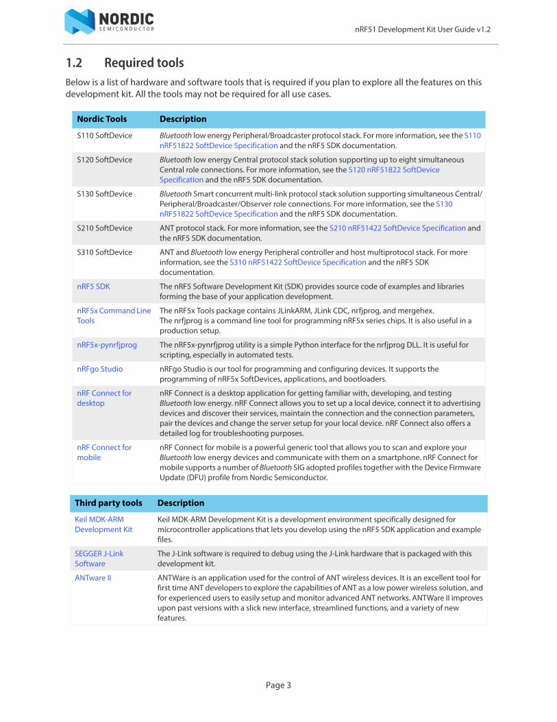
1.2 Required toolsBelow is a list of hardware and software tools that is required if you plan to explore all the features on this development kit. All the tools may not be required for all use cases.
Nordic Tools Description
S110 SoftDevice Bluetooth low energy Peripheral/Broadcaster protocol stack. For more information, see the S110 nRF51822 SoftDevice Specification and the nRF5 SDK documentation.
S120 SoftDevice Bluetooth low energy Central protocol stack solution supporting up to eight simultaneous Central role connections. For more information, see the S120 nRF51822 SoftDevice Specification and the nRF5 SDK documentation.
S130 SoftDevice Bluetooth Smart concurrent multi-link protocol stack solution supporting simultaneous Central/Peripheral/Broadcaster/Observer role connections. For more information, see the S130 nRF51822 SoftDevice Specification and the nRF5 SDK documentation.
S210 SoftDevice ANT protocol stack. For more information, see the S210 nRF51422 SoftDevice Specification and the nRF5 SDK documentation.
S310 SoftDevice ANT and Bluetooth low energy Peripheral controller and host multiprotocol stack. For more information, see the S310 nRF51422 SoftDevice Specification and the nRF5 SDK documentation.
nRF5 SDK The nRF5 Software Development Kit (SDK) provides source code of examples and libraries forming the base of your application development.
nRF5x Command Line Tools
The nRF5x Tools package contains JLinkARM, JLink CDC, nrfjprog, and mergehex. The nrfjprog is a command line tool for programming nRF5x series chips. It is also useful in a production setup.
nRF5x-pynrfjprog The nRF5x-pynrfjprog utility is a simple Python interface for the nrfjprog DLL. It is useful for scripting, especially in automated tests.
nRFgo Studio nRFgo Studio is our tool for programming and configuring devices. It supports the programming of nRF5x SoftDevices, applications, and bootloaders.
nRF Connect for desktop
nRF Connect is a desktop application for getting familiar with, developing, and testing Bluetooth low energy. nRF Connect allows you to set up a local device, connect it to advertising devices and discover their services, maintain the connection and the connection parameters, pair the devices and change the server setup for your local device. nRF Connect also offers a detailed log for troubleshooting purposes.
nRF Connect for mobile
nRF Connect for mobile is a powerful generic tool that allows you to scan and explore your Bluetooth low energy devices and communicate with them on a smartphone. nRF Connect for mobile supports a number of Bluetooth SIG adopted profiles together with the Device Firmware Update (DFU) profile from Nordic Semiconductor.
Third party tools Description
Keil MDK-ARM Development Kit
Keil MDK-ARM Development Kit is a development environment specifically designed for microcontroller applications that lets you develop using the nRF5 SDK application and example files.
SEGGER J-Link Software
The J-Link software is required to debug using the J-Link hardware that is packaged with this development kit.
ANTware II ANTWare is an application used for the control of ANT wireless devices. It is an excellent tool for first time ANT developers to explore the capabilities of ANT as a low power wireless solution, and for experienced users to easily setup and monitor advanced ANT networks. ANTWare II improves upon past versions with a slick new interface, streamlined functions, and a variety of new features.
Page 3
nRF51 Development Kit User Guide v1.2
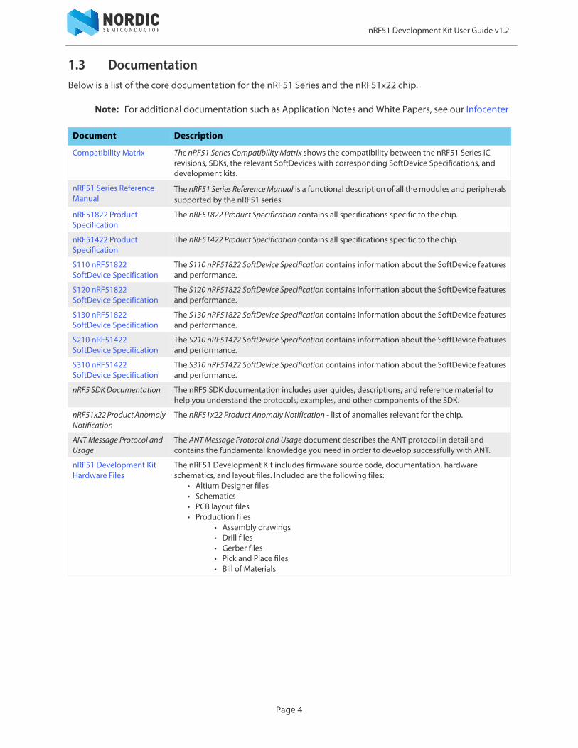
1.3 DocumentationBelow is a list of the core documentation for the nRF51 Series and the nRF51x22 chip.
Note: For additional documentation such as Application Notes and White Papers, see our Infocenter
Document Description
Compatibility Matrix The nRF51 Series Compatibility Matrix shows the compatibility between the nRF51 Series IC revisions, SDKs, the relevant SoftDevices with corresponding SoftDevice Specifications, and development kits.
nRF51 Series Reference Manual
The nRF51 Series Reference Manual is a functional description of all the modules and peripherals supported by the nRF51 series.
nRF51822 Product Specification
The nRF51822 Product Specification contains all specifications specific to the chip.
nRF51422 Product Specification
The nRF51422 Product Specification contains all specifications specific to the chip.
S110 nRF51822 SoftDevice Specification
The S110 nRF51822 SoftDevice Specification contains information about the SoftDevice features and performance.
S120 nRF51822 SoftDevice Specification
The S120 nRF51822 SoftDevice Specification contains information about the SoftDevice features and performance.
S130 nRF51822 SoftDevice Specification
The S130 nRF51822 SoftDevice Specification contains information about the SoftDevice features and performance.
S210 nRF51422 SoftDevice Specification
The S210 nRF51422 SoftDevice Specification contains information about the SoftDevice features and performance.
S310 nRF51422 SoftDevice Specification
The S310 nRF51422 SoftDevice Specification contains information about the SoftDevice features and performance.
nRF5 SDK Documentation The nRF5 SDK documentation includes user guides, descriptions, and reference material to help you understand the protocols, examples, and other components of the SDK.
nRF51x22 Product Anomaly Notification
The nRF51x22 Product Anomaly Notification - list of anomalies relevant for the chip.
ANT Message Protocol and Usage
The ANT Message Protocol and Usage document describes the ANT protocol in detail and contains the fundamental knowledge you need in order to develop successfully with ANT.
nRF51 Development Kit Hardware Files
The nRF51 Development Kit includes firmware source code, documentation, hardware schematics, and layout files. Included are the following files:
• Altium Designer files• Schematics• PCB layout files• Production files
• Assembly drawings• Drill files• Gerber files• Pick and Place files• Bill of Materials
Page 4
nRF51 Development Kit User Guide v1.2
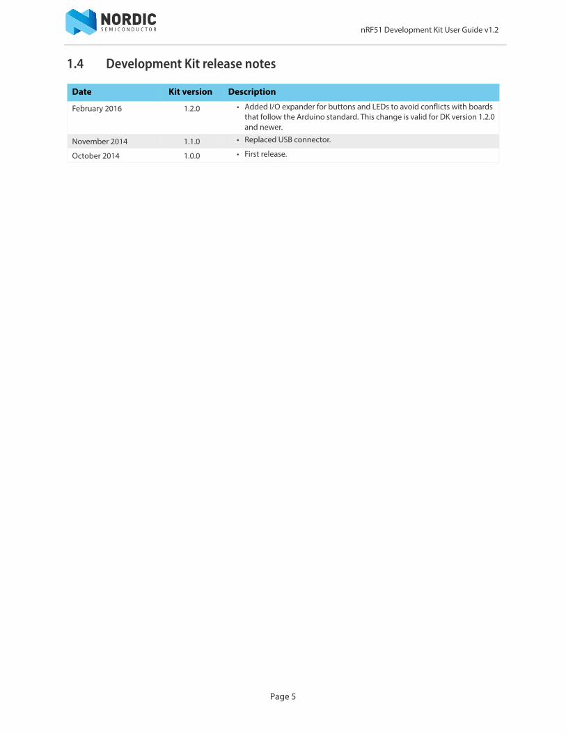
1.4 Development Kit release notes
Date Kit version Description
February 2016 1.2.0 • Added I/O expander for buttons and LEDs to avoid conflicts with boards that follow the Arduino standard. This change is valid for DK version 1.2.0 and newer.
November 2014 1.1.0 • Replaced USB connector.
October 2014 1.0.0 • First release.
Page 5
Page 6
nRF51 Development Kit User Guide v1.2
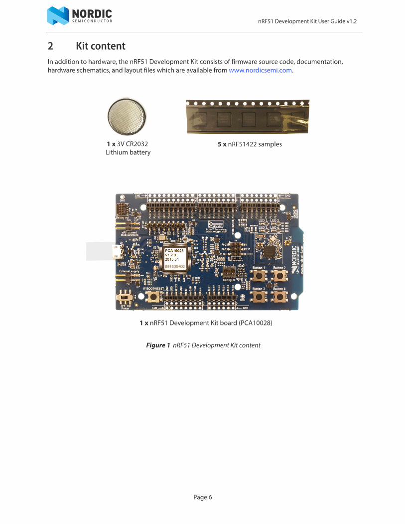
2 Kit contentIn addition to hardware, the nRF51 Development Kit consists of firmware source code, documentation, hardware schematics, and layout files which are available from www.nordicsemi.com.
Figure 1 nRF51 Development Kit content
1 x 3V CR2032Lithium battery
5 x nRF51422 samples
1 x nRF51 Development Kit board (PCA10028)
nRF51 Development Kit User Guide v1.2
Page 7
3 Getting startedThis section shows you how to get access to the tools, libraries, and documentation.
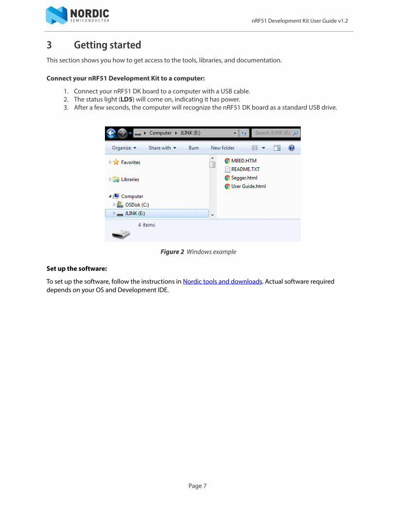
Connect your nRF51 Development Kit to a computer:
1. Connect your nRF51 DK board to a computer with a USB cable.2. The status light (LD5) will come on, indicating it has power.3. After a few seconds, the computer will recognize the nRF51 DK board as a standard USB drive.
Figure 2 Windows example
Set up the software:
To set up the software, follow the instructions in Nordic tools and downloads. Actual software required depends on your OS and Development IDE.
nRF51 Development Kit User Guide v1.2
Page 8
4 Start developingAfter you have set up the development kit and installed the toolchain, it is time to start developing.
There are several ways to continue from here. For more information, see the following nRF5 SDK instructions:
• Running precompiled examplesSee how you can quickly test a precompiled example without having to use the full tool-chain. It is a matter of copying and pasting a precompiled hex file onto your development kit board.
• Compiling and running a first exampleTest that you have set up your toolchain correctly by compiling, programming and running a very simple example.
• Running examples that use a SoftDeviceBefore you can run more advanced examples that use Bluetooth® or ANT™, you must first program the SoftDevice on the board.
nRF51 Development Kit User Guide v1.2
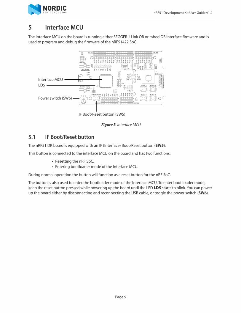
5 Interface MCUThe Interface MCU on the board is running either SEGGER J-Link OB or mbed OB interface firmware and is used to program and debug the firmware of the nRF51422 SoC.
Figure 3 Interface MCU
5.1 IF Boot/Reset buttonThe nRF51 DK board is equipped with an IF (Interface) Boot/Reset button (SW5).
This button is connected to the interface MCU on the board and has two functions:
• Resetting the nRF SoC.• Entering bootloader mode of the Interface MCU.
During normal operation the button will function as a reset button for the nRF SoC.
The button is also used to enter the bootloader mode of the Interface MCU. To enter boot loader mode, keep the reset button pressed while powering up the board until the LED LD5 starts to blink. You can power up the board either by disconnecting and reconnecting the USB cable, or toggle the power switch (SW6).
Interface MCU
IF Boot/Reset button (SW5)
Power switch (SW6)
LD5
Page 9
nRF51 Development Kit User Guide v1.2
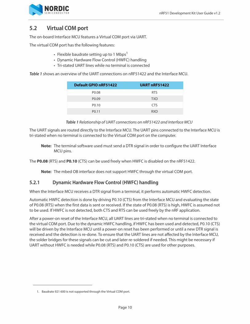
5.2 Virtual COM portThe on-board Interface MCU features a Virtual COM port via UART.
The virtual COM port has the following features:
• Flexible baudrate setting up to 1 Mbps1
• Dynamic Hardware Flow Control (HWFC) handling• Tri-stated UART lines while no terminal is connected
Table 1 shows an overview of the UART connections on nRF51422 and the Interface MCU.
Table 1 Relationship of UART connections on nRF51422 and Interface MCU
The UART signals are routed directly to the Interface MCU. The UART pins connected to the Interface MCU is tri-stated when no terminal is connected to the Virtual COM port on the computer.
Note: The terminal software used must send a DTR signal in order to configure the UART Interface MCU pins.
The P0.08 (RTS) and P0.10 (CTS) can be used freely when HWFC is disabled on the nRF51422.
Note: The mbed OB interface does not support HWFC through the virtual COM port.
5.2.1 Dynamic Hardware Flow Control (HWFC) handling
When the Interface MCU receives a DTR signal from a terminal, it performs automatic HWFC detection.
Automatic HWFC detection is done by driving P0.10 (CTS) from the Interface MCU and evaluating the state of P0.08 (RTS) when the first data is sent or received. If the state of P0.08 (RTS) is high, HWFC is assumed not to be used. If HWFC is not detected, both CTS and RTS can be used freely by the nRF application.
After a power-on reset of the Interface MCU, all UART lines are tri-stated when no terminal is connected to the virtual COM port. Due to the dynamic HWFC handling, if HWFC has been used and detected, P0.10 (CTS) will be driven by the Interface MCU until a power-on reset has been performed or until a new DTR signal is received and the detection is re-done. To ensure that the UART lines are not affected by the Interface MCU, the solder bridges for these signals can be cut and later re-soldered if needed. This might be necessary if UART without HWFC is needed while P0.08 (RTS) and P0.10 (CTS) are used for other purposes.
1. Baudrate 921 600 is not supported through the Virtual COM port.
Default GPIO nRF51422 UART nRF51422
P0.08 RTS
P0.09 TXD
P0.10 CTS
P0.11 RXD
Page 10
nRF51 Development Kit User Guide v1.2
5.3 Interface MCU firmwareThe on board Interface MCU is factory programmed with an mbed compliant bootloader, this feature enables the ability to swap interface firmware between the factory preloaded SEGGER J-Link OB and the nRF51 mbed interface firmware, see section 5.1 “IF Boot/Reset button” on page 9 on how to enter the bootloader.
To swap Interface MCU firmware, simply drag the interface image (.bin) into the mounted bootloader drive on the connected computer and power cycle the board.
Both the nRF51 mbed interface firmware and the J-Link OB image can be downloaded from www.nordicsemi.com.
Note: The J-Link OB interface bin downloaded from www.nordicsemi.com is never the latest one. If you want to use the latest J-Link OB firmware version, download the latest SEGGER J-Link software from www.segger.com and open a debug session to update to the latest J-Link OB firmware version.
Note: The J-Link serial number is linked to the Interface MCU and will not change even when swapping the Interface MCU firmware, so it can be useful to write the serial number on a sticker on the board.
Note: When in bootloader mode, do not drag and drop any files except those downloaded from www.nordicsemi.com for use with the Interface MCU. If a wrong file is used, it can overwrite the bootloader and ruin the Interface MCU firmware without the possibility of recovery.
5.4 MSDThe interface MCU features a mass storage device (MSD). This makes the development kit appear as anexternal drive on your computer.This drive can be used for drag-and-drop programming. Files cannot be stored on this drive. By copying a HEX file to the drive, the interface MCU will program the file to the device.
Note: Windows might try to defragment the MSD part of the interface MCU. If this happens, the interface MCU will disconnect and be unresponsive. To return to normal operation, the development kit must be power cycled.
Note: Your antivirus software might try to scan the MSD part of the interface MCU. It is known that a certain antivirus program triggers a false positive alert in one of the files and quarantines the unit. If this happens, the interface MCU will become unresponsive.
Note: If the computer is set up to boot from USB, it can try to boot from the development kit if the development kit is connected during boot. This could be avoided by unplugging the development kit before a computer restart, or changing the boot sequence of the computer.
You can also disable the MSD of the kit by using the msddisable command in J-Link Commander. To enable, use the msdenable command. These commands take effect after a power cycle of the development kit and should stay this way until changed again.
Page 11
nRF51 Development Kit User Guide v1.2
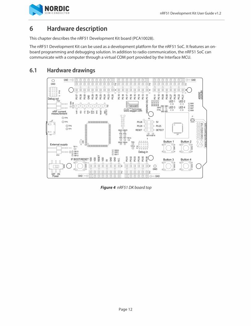
6 Hardware descriptionThis chapter describes the nRF51 Development Kit board (PCA10028).
The nRF51 Development Kit can be used as a development platform for the nRF51 SoC. It features an on-board programming and debugging solution. In addition to radio communication, the nRF51 SoC can communicate with a computer through a virtual COM port provided by the Interface MCU.
6.1 Hardware drawings
Figure 4 nRF51 DK board top
Page 12
nRF51 Development Kit User Guide v1.2
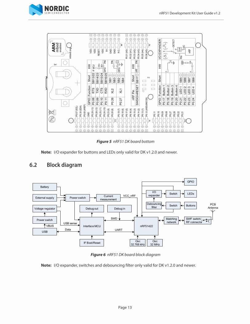
Figure 5 nRF51 DK board bottom
Note: I/O expander for buttons and LEDs only valid for DK v1.2.0 and newer.
6.2 Block diagram
Figure 6 nRF51 DK board block diagram
Note: I/O expander, switches and debouncing filter only valid for DK v1.2.0 and newer.
External supply Current measurement
USB
Battery
ButtonsVoltage regulator
LEDs
GPIO
nRF51422
PCBAntenna
Interface MCUVBUSUSB sense
Data
Osc 32.768 kHzIF Boot/Reset
UART
SWD
VCC_nRF
Osc 32 MHz
Debug inDebug out
Power switch
Power switch Matchingnetwork
SWF switch/RF connector
I/O expander
Debouncing filter Switch
Switch
Page 13
nRF51 Development Kit User Guide v1.2
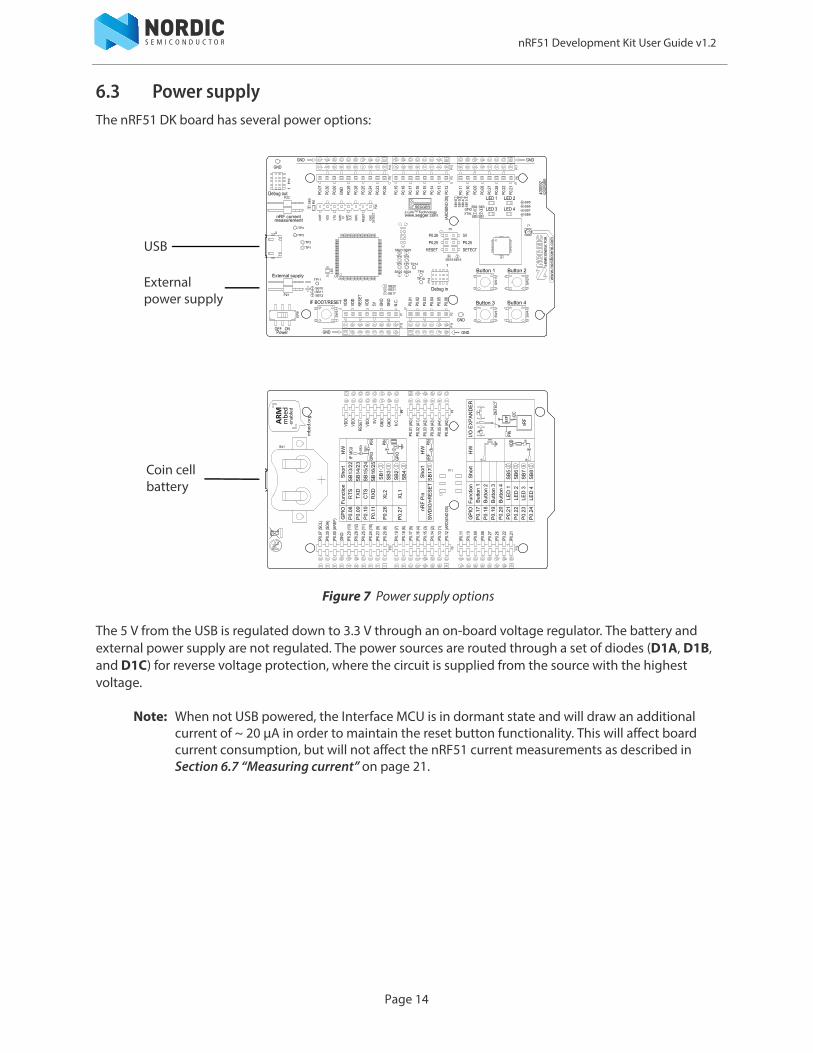
6.3 Power supply The nRF51 DK board has several power options:
Figure 7 Power supply options
The 5 V from the USB is regulated down to 3.3 V through an on-board voltage regulator. The battery and external power supply are not regulated. The power sources are routed through a set of diodes (D1A, D1B, and D1C) for reverse voltage protection, where the circuit is supplied from the source with the highest voltage.
Note: When not USB powered, the Interface MCU is in dormant state and will draw an additional current of ~ 20 μA in order to maintain the reset button functionality. This will affect board current consumption, but will not affect the nRF51 current measurements as described in Section 6.7 “Measuring current” on page 21.
USB
Externalpower supply
Coin cellbattery
Page 14
nRF51 Development Kit User Guide v1.2
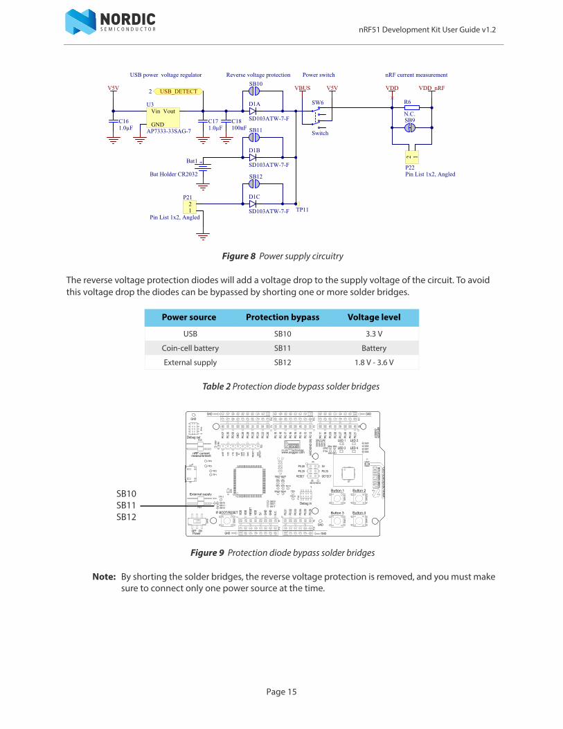
Figure 8 Power supply circuitry
The reverse voltage protection diodes will add a voltage drop to the supply voltage of the circuit. To avoid this voltage drop the diodes can be bypassed by shorting one or more solder bridges.
Table 2 Protection diode bypass solder bridges
Figure 9 Protection diode bypass solder bridges
Note: By shorting the solder bridges, the reverse voltage protection is removed, and you must make sure to connect only one power source at the time.
Power source Protection bypass Voltage level
USB SB10 3.3 V
Coin-cell battery SB11 Battery
External supply SB12 1.8 V - 3.6 V
C18100nF
C171.0μF
C161.0μF
+Bat1
Bat Holder CR2032
Vin
GND
VoutU3
AP7333-33SAG-7
D1A
SD103ATW-7-F
D1B
SD103ATW-7-F
D1C
SD103ATW-7-F
VDD
R6
N.C.SB9
VDD_nRF
SW6
Switch
12
P21
Pin List 1x2, Angled
VBUSSB10
SB11
SB12
TP11
12
P22Pin List 1x2, Angled
Power switchUSB power voltage regulator nRF current measurementReverse voltage protection
USB_DETECT2 V5VV5V
SB10SB11SB12
Page 15
nRF51 Development Kit User Guide v1.2
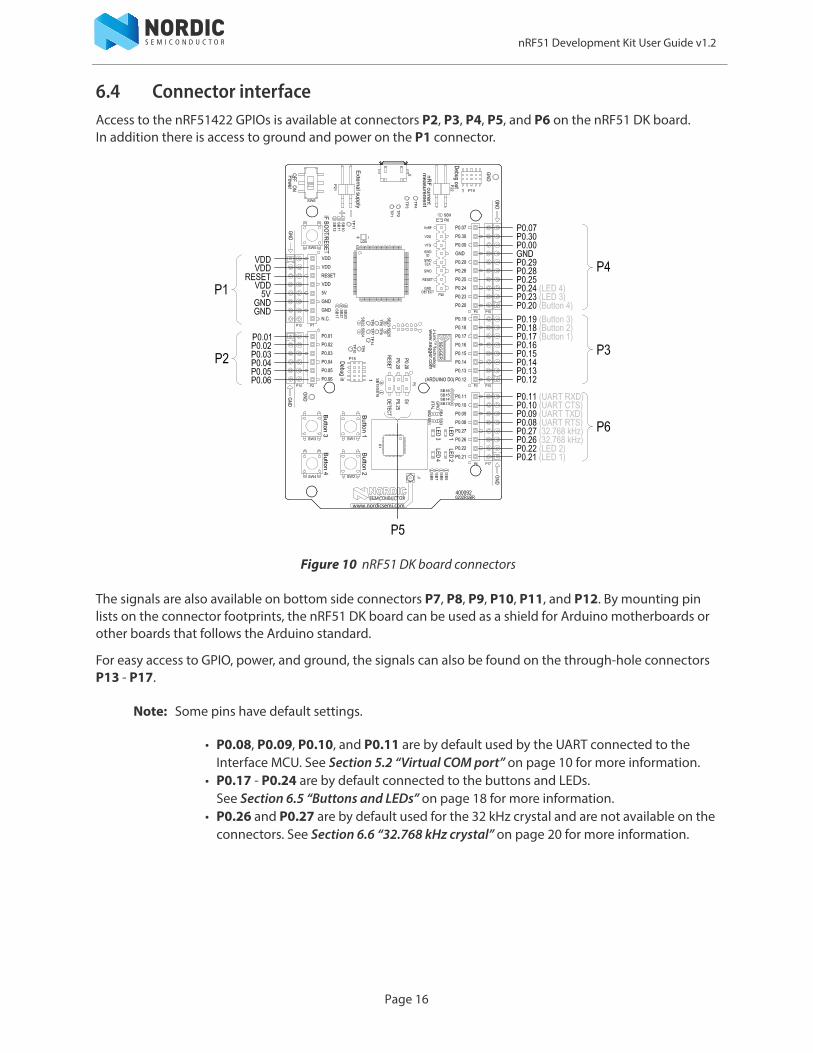
6.4 Connector interfaceAccess to the nRF51422 GPIOs is available at connectors P2, P3, P4, P5, and P6 on the nRF51 DK board. In addition there is access to ground and power on the P1 connector.
Figure 10 nRF51 DK board connectors
The signals are also available on bottom side connectors P7, P8, P9, P10, P11, and P12. By mounting pin lists on the connector footprints, the nRF51 DK board can be used as a shield for Arduino motherboards or other boards that follows the Arduino standard.
For easy access to GPIO, power, and ground, the signals can also be found on the through-hole connectors P13 - P17.
Note: Some pins have default settings.
• P0.08, P0.09, P0.10, and P0.11 are by default used by the UART connected to the Interface MCU. See Section 5.2 “Virtual COM port” on page 10 for more information.
• P0.17 - P0.24 are by default connected to the buttons and LEDs. See Section 6.5 “Buttons and LEDs” on page 18 for more information.
• P0.26 and P0.27 are by default used for the 32 kHz crystal and are not available on the connectors. See Section 6.6 “32.768 kHz crystal” on page 20 for more information.
Page 16
nRF51 Development Kit User Guide v1.2
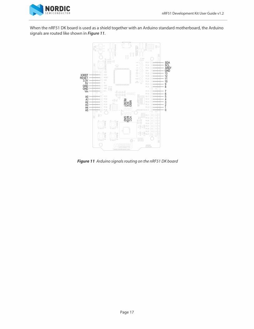
When the nRF51 DK board is used as a shield together with an Arduino standard motherboard, the Arduino signals are routed like shown in Figure 11.
Figure 11 Arduino signals routing on the nRF51 DK board
Page 17
nRF51 Development Kit User Guide v1.2
6.5 Buttons and LEDsThe four buttons and four LEDs on nRF51 DK board are connected to dedicated I/Os on the nRF51422 SoC. The connections are shown in Table 3.
Table 3 Button and LED connection
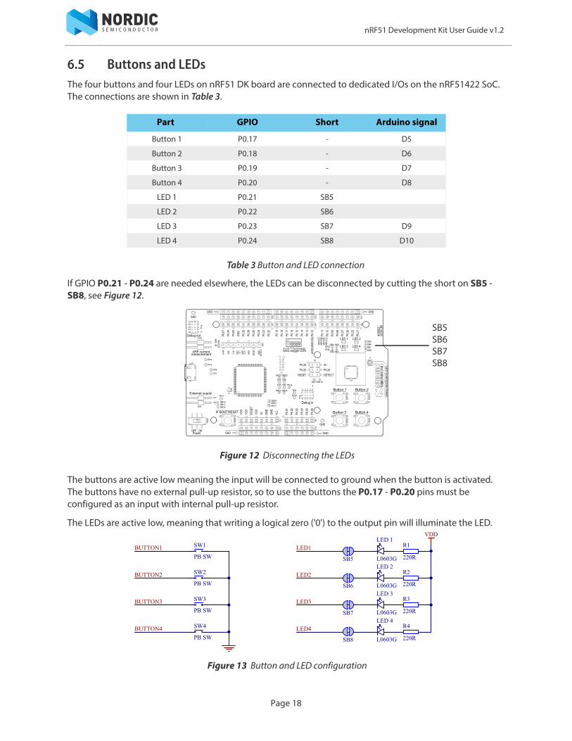
If GPIO P0.21 - P0.24 are needed elsewhere, the LEDs can be disconnected by cutting the short on SB5 - SB8, see Figure 12.
Figure 12 Disconnecting the LEDs
The buttons are active low meaning the input will be connected to ground when the button is activated. The buttons have no external pull-up resistor, so to use the buttons the P0.17 - P0.20 pins must be configured as an input with internal pull-up resistor.
The LEDs are active low, meaning that writing a logical zero ('0') to the output pin will illuminate the LED.
Figure 13 Button and LED configuration
Part GPIO Short Arduino signal
Button 1 P0.17 - D5
Button 2 P0.18 - D6
Button 3 P0.19 - D7
Button 4 P0.20 - D8
LED 1 P0.21 SB5
LED 2 P0.22 SB6
LED 3 P0.23 SB7 D9
LED 4 P0.24 SB8 D10
SB5SB6SB7SB8
SW2
PB SW
SW1
PB SW
SW3
PB SW
LED 2
L0603G
R2
220R
R1
220R
LED 1
L0603G
SB6
SW4
PB SW
LED 3
L0603GLED 4
L0603G
R3
220RSB7
R4
220RSB8
SB5
VDD
BUTTON1
BUTTON2
BUTTON3
BUTTON4
LED1
LED2
LED3
LED4
Page 18
nRF51 Development Kit User Guide v1.2
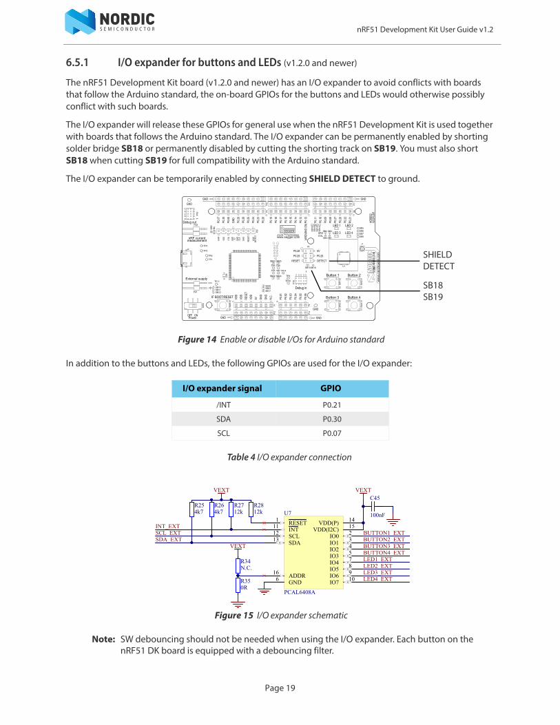
6.5.1 I/O expander for buttons and LEDs (v1.2.0 and newer)
The nRF51 Development Kit board (v1.2.0 and newer) has an I/O expander to avoid conflicts with boards that follow the Arduino standard, the on-board GPIOs for the buttons and LEDs would otherwise possibly conflict with such boards.
The I/O expander will release these GPIOs for general use when the nRF51 Development Kit is used together with boards that follows the Arduino standard. The I/O expander can be permanently enabled by shorting solder bridge SB18 or permanently disabled by cutting the shorting track on SB19. You must also short SB18 when cutting SB19 for full compatibility with the Arduino standard.
The I/O expander can be temporarily enabled by connecting SHIELD DETECT to ground.
Figure 14 Enable or disable I/Os for Arduino standard
In addition to the buttons and LEDs, the following GPIOs are used for the I/O expander:
Table 4 I/O expander connection
Figure 15 I/O expander schematic
Note: SW debouncing should not be needed when using the I/O expander. Each button on the nRF51 DK board is equipped with a debouncing filter.
I/O expander signal GPIO
/INT P0.21
SDA P0.30
SCL P0.07
SHIELD
SB18SB19
DETECT
SDA13
VDD(I2C) 15
ADDR16
SCL12
RESET1
INT11
IO3 5
GND6
VDD(P) 14
IO2 4IO1 3IO0 2
IO7 10IO6 9IO5 8IO4 7
U7
PCAL6408A
C45
100nF
R254k7
R264k7
R2712k
R2812k
R34N.C.
R350R
VEXTVEXT
BUTTON1_EXTBUTTON2_EXTBUTTON3_EXTBUTTON4_EXT
LED4_EXTLED3_EXTLED2_EXTLED1_EXT
SDA_EXTSCL_EXTINT_EXT
VEXT
Page 19
nRF51 Development Kit User Guide v1.2
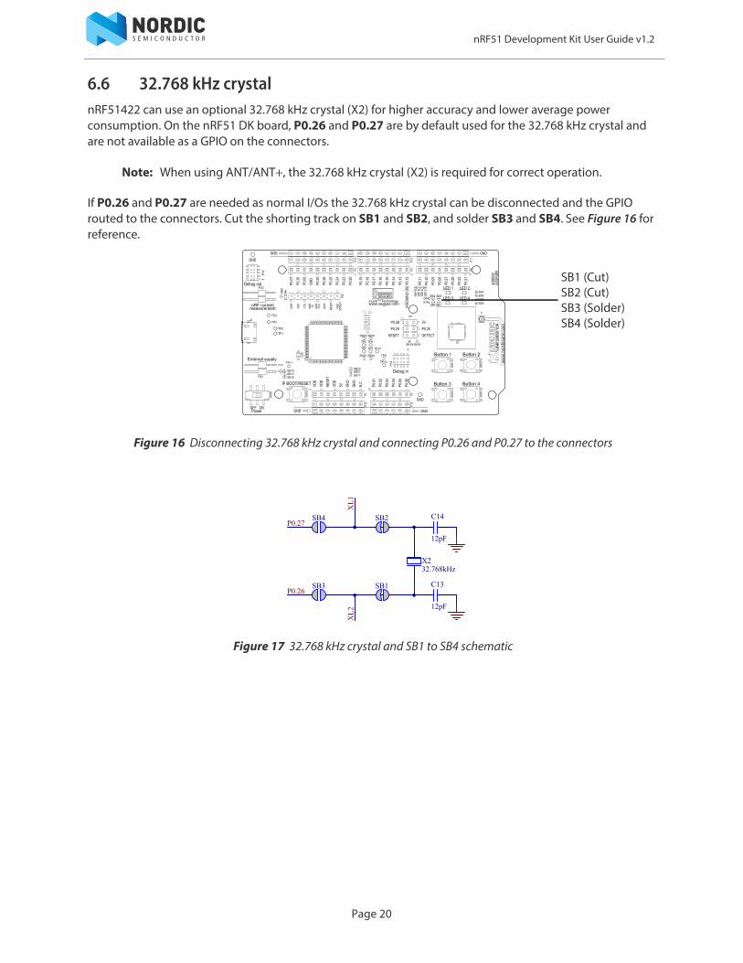
6.6 32.768 kHz crystalnRF51422 can use an optional 32.768 kHz crystal (X2) for higher accuracy and lower average power consumption. On the nRF51 DK board, P0.26 and P0.27 are by default used for the 32.768 kHz crystal and are not available as a GPIO on the connectors.
Note: When using ANT/ANT+, the 32.768 kHz crystal (X2) is required for correct operation.
If P0.26 and P0.27 are needed as normal I/Os the 32.768 kHz crystal can be disconnected and the GPIO routed to the connectors. Cut the shorting track on SB1 and SB2, and solder SB3 and SB4. See Figure 16 for reference.
Figure 16 Disconnecting 32.768 kHz crystal and connecting P0.26 and P0.27 to the connectors
Figure 17 32.768 kHz crystal and SB1 to SB4 schematic
SB1 (Cut)SB2 (Cut)SB3 (Solder)SB4 (Solder)
C14
12pF
C13
12pF
X232.768kHz
P0.26
P0.27
XL2
XL1
SB3
SB4
SB1
SB2
Page 20
nRF51 Development Kit User Guide v1.2
6.7 Measuring currentThe current drawn by the nRF51422 SoC can be monitored on the nRF51 DK board.
There are several types of test equipment that can be used to measure current, each type has some advantages and some disadvantages. The different test equipment types are:
• Power analyzer• Oscilloscope• Ampere-meter• Power Profiler Kit
Power analyzer and Power Profiler Kit measurements will not be described in this document. See Power Profiler Kit documentation for more information.
See Section 6.7.2 “Using an oscilloscope for current profile measurement” on page 23 for instructions.
See Section 6.7.3 “Using an ampere-meter for current measurement” on page 24 for instructions.
Note: When measuring the current consumption:•
• Do not use the USB connector to power the board during current measurements. Power the board from a coin cell battery, or use an external power supply on the External Supply connector P21.
• The current measurements will become unreliable when a serial terminal is connected to the Virtual COM port.
• After programming the nRF51422 SoC, the USB must be disconnected and the development kit power cycled to reset the debugger chip before current measurement.
Page 21
nRF51 Development Kit User Guide v1.2
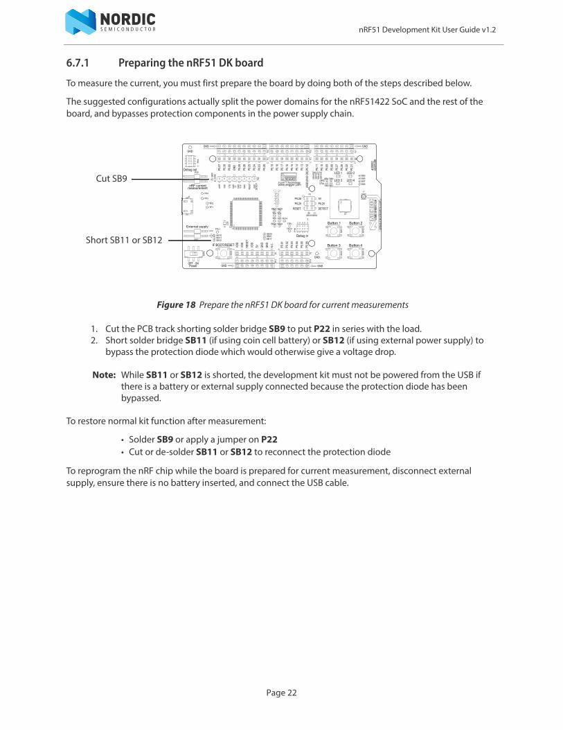
6.7.1 Preparing the nRF51 DK board
To measure the current, you must first prepare the board by doing both of the steps described below.
The suggested configurations actually split the power domains for the nRF51422 SoC and the rest of the board, and bypasses protection components in the power supply chain.
Figure 18 Prepare the nRF51 DK board for current measurements
1. Cut the PCB track shorting solder bridge SB9 to put P22 in series with the load. 2. Short solder bridge SB11 (if using coin cell battery) or SB12 (if using external power supply) to
bypass the protection diode which would otherwise give a voltage drop.
Note: While SB11 or SB12 is shorted, the development kit must not be powered from the USB if there is a battery or external supply connected because the protection diode has been bypassed.
To restore normal kit function after measurement:
• Solder SB9 or apply a jumper on P22• Cut or de-solder SB11 or SB12 to reconnect the protection diode
To reprogram the nRF chip while the board is prepared for current measurement, disconnect external supply, ensure there is no battery inserted, and connect the USB cable.
Cut SB9
Short SB11 or SB12
Page 22
nRF51 Development Kit User Guide v1.2
6.7.2 Using an oscilloscope for current profile measurement
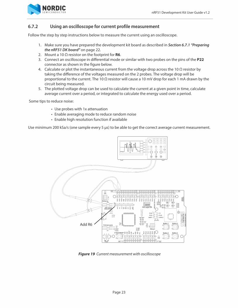
Follow the step by step instructions below to measure the current using an oscilloscope.
1. Make sure you have prepared the development kit board as described in Section 6.7.1 “Preparing the nRF51 DK board” on page 22.
2. Mount a 10 Ω resistor on the footprint for R6. 3. Connect an oscilloscope in differential mode or similar with two probes on the pins of the P22
connector as shown in the figure below. 4. Calculate or plot the instantaneous current from the voltage drop across the 10 Ω resistor by
taking the difference of the voltages measured on the 2 probes. The voltage drop will be proportional to the current. The 10 Ω resistor will cause a 10 mV drop for each 1 mA drawn by the circuit being measured.
5. The plotted voltage drop can be used to calculate the current at a given point in time, calculate average current over a period, or integrated to calculate the energy used over a period.
Some tips to reduce noise:
• Use probes with 1x attenuation• Enable averaging mode to reduce random noise• Enable high resolution function if available
Use minimum 200 kSa/s (one sample every 5 μs) to be able to get the correct average current measurement.
Figure 19 Current measurement with oscilloscope
Add R6
Page 23
nRF51 Development Kit User Guide v1.2
6.7.3 Using an ampere-meter for current measurement
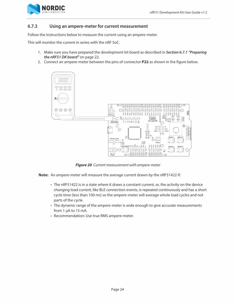
Follow the instructions below to measure the current using an ampere-meter.
This will monitor the current in series with the nRF SoC.
1. Make sure you have prepared the development kit board as described in Section 6.7.1 “Preparing the nRF51 DK board” on page 22.
2. Connect an ampere-meter between the pins of connector P22 as shown in the figure below.
Figure 20 Current measurement with ampere-meter
Note: An ampere-meter will measure the average current drawn by the nRF51422 if:
• The nRF51422 is in a state where it draws a constant current, or, the activity on the device changing load current, like BLE connection events, is repeated continuously and has a short cycle time (less than 100 ms) so the ampere-meter will average whole load cycles and not parts of the cycle.
• The dynamic range of the ampere-meter is wide enough to give accurate measurements from 1 μA to 15 mA.
• Recommendation: Use true RMS ampere-meter.
Page 24
nRF51 Development Kit User Guide v1.2
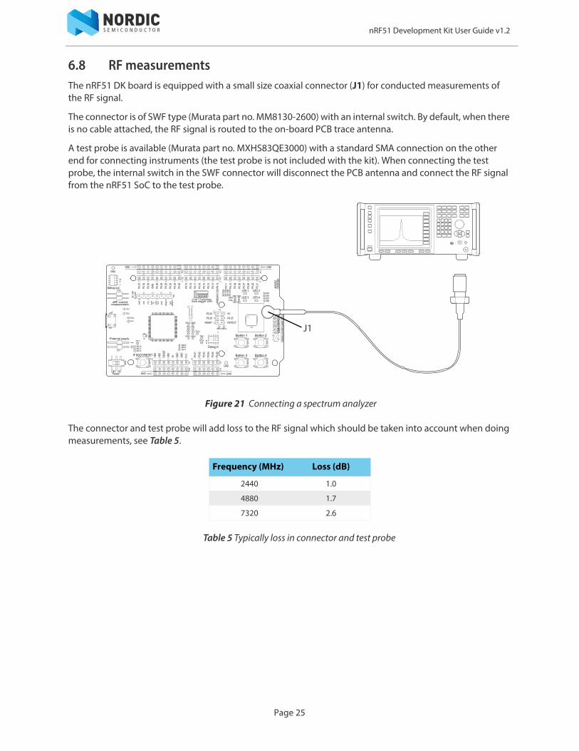
6.8 RF measurementsThe nRF51 DK board is equipped with a small size coaxial connector (J1) for conducted measurements of the RF signal.
The connector is of SWF type (Murata part no. MM8130-2600) with an internal switch. By default, when there is no cable attached, the RF signal is routed to the on-board PCB trace antenna.
A test probe is available (Murata part no. MXHS83QE3000) with a standard SMA connection on the other end for connecting instruments (the test probe is not included with the kit). When connecting the test probe, the internal switch in the SWF connector will disconnect the PCB antenna and connect the RF signal from the nRF51 SoC to the test probe.
Figure 21 Connecting a spectrum analyzer
The connector and test probe will add loss to the RF signal which should be taken into account when doing measurements, see Table 5.
Table 5 Typically loss in connector and test probe
Frequency (MHz) Loss (dB)
2440 1.0
4880 1.7
7320 2.6
J1
Page 25
nRF51 Development Kit User Guide v1.2
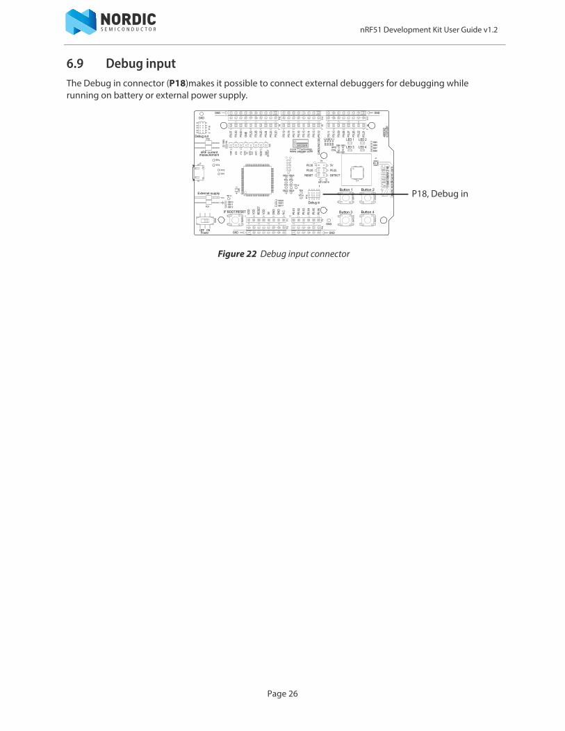
6.9 Debug inputThe Debug in connector (P18)makes it possible to connect external debuggers for debugging while running on battery or external power supply.
Figure 22 Debug input connector
P18, Debug in
Page 26
nRF51 Development Kit User Guide v1.2
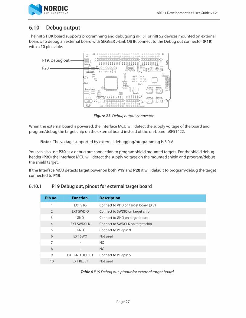
6.10 Debug outputThe nRF51 DK board supports programming and debugging nRF51 or nRF52 devices mounted on external boards. To debug an external board with SEGGER J-Link OB IF, connect to the Debug out connector (P19) with a 10 pin cable.
Figure 23 Debug output connector
When the external board is powered, the Interface MCU will detect the supply voltage of the board and program/debug the target chip on the external board instead of the on-board nRF51422.
Note: The voltage supported by external debugging/programming is 3.0 V.
You can also use P20 as a debug out connection to program shield mounted targets. For the shield debug header (P20) the Interface MCU will detect the supply voltage on the mounted shield and program/debug the shield target.
If the Interface MCU detects target power on both P19 and P20 it will default to program/debug the target connected to P19.
6.10.1 P19 Debug out, pinout for external target board
Table 6 P19 Debug out, pinout for external target board
Pin no. Function Description
1 EXT VTG Connect to VDD on target board (3 V)
2 EXT SWDIO Connect to SWDIO on target chip
3 GND Connect to GND on target board
4 EXT SWDCLK Connect to SWDCLK on target chip
5 GND Connect to P19 pin 9
6 EXT SWO Not used
7 - NC
8 - NC
9 EXT GND DETECT Connect to P19 pin 5
10 EXT RESET Not used
P19, Debug out
P20
Page 27
nRF51 Development Kit User Guide v1.2
6.10.2 P20 Debug out, pinout for shield target board
Table 7 P20 Debug out, pinout for shield target board
6.11 Solderbridge configuration
Table 8 Solderbridges for all DK versions
Pin no. Function Description
1 VnRF nRF SoC power net
2 VDD DK power net
3 SH VTG Connect to VDD on shield target board that is self-powered with 3 V
4 SH SWDIO Connect to SWDIO on target chip
5 SH SWDCLK Connect to SWDCLK on target chip
6 SH SWO Not used
7 SH RESET Not used
8 SH GND DETECT Connect to GND on shield target board and GND on nRF51 DK
Solderbridge Default Function
SB1 Closed Cut to disconnect the 32.768 kHz from P0.26.
SB2 Closed Cut to disconnect the 32.768 kHz from P0.27.
SB3 Open Short to enable P0.26 as normal GPIO.
SB4 Open Short to enable P0.27 as normal GPIO.
SB5 Closed Cut to disconnect LED1.
SB6 Closed Cut to disconnect LED2.
SB7 Closed Cut to disconnect LED3.
SB8 Closed Cut to disconnect LED4.
SB9 Closed Cut for current measurements.
SB10 Open Short to bypass the reverse voltage protection diode on the USB power.
SB11 Open Short to bypass the reverse voltage protection diode on the coin-cell battery power.
SB12 Open Short to bypass the reverse voltage protection diode on the external power supply.
SB13 Closed Cut to disconnect P0.08 from the connector interface.
SB14 Closed Cut to disconnect P0.09 from the connector interface.
SB15 Closed Cut to disconnect P0.10 from the connector interface.
SB16 Closed Cut to disconnect P0.11 from the connector interface.
SB17 Open Short to connect SWDIO/nRF_RESET to the connector interface RESET.
Solderbridge Default Function
SB18 Open Short to permanently enable the I/O expander.
SB19 Closed Cut to permanently disable the I/O expander.
SB20 Closed Cut to isolate SWDIO from nRF51422 to the Interface MCU.
Page 28
nRF51 Development Kit User Guide v1.2
Table 9 Solderbridges for DK v1.2.0 and newer.
SB21 Closed Cut to isolate SWDCLK from nRF51422 to the Interface MCU.
SB22 Closed Cut to isolate P0.08 from nRF51422 to the Interface MCU.
SB23 Closed Cut to isolate P0.09 from nRF51422 to the Interface MCU.
SB24 Closed Cut to isolate P0.10 from nRF51422 to the Interface MCU.
SB25 Closed Cut to isolate P0.11 from nRF51422 to the Interface MCU.
Solderbridge Default Function
Page 29
nRF51 Development Kit User Guide v1.2
Liability disclaimerNordic Semiconductor ASA reserves the right to make changes without further notice to the product to improve reliability, function or design. Nordic Semiconductor ASA does not assume any liability arising out of the application or use of any product or circuits described herein.
Life support applicationsNordic Semiconductor’s products are not designed for use in life support appliances, devices, or systems where malfunction of these products can reasonably be expected to result in personal injury. Nordic Semiconductor ASA customers using or selling these products for use in such applications do so at their own risk and agree to fully indemnify Nordic Semiconductor ASA for any damages resulting from such improper use or sale.
Contact detailsFor your nearest distributor, please visit http://www.nordicsemi.com.Information regarding product updates, downloads, and technical support can be accessed through your My Page account on our homepage.
Main office:
Phone: +47 72 89 89 00Fax: +47 72 89 89 89
Otto Nielsens veg 127052 TrondheimNorway
Mailing address: Nordic SemiconductorP.O. Box 23367004 TrondheimNorway
Page 30
nRF51 Development Kit User Guide v1.2
Revision history
ARM statementKeil, μVision, and Cortex are trademarks of ARM Limited. All other brands or product names are the property of their respective holders.
Date Version Description
February 2017 1.2 Added:• Chapter 4 “Start developing” on page 8• Section 5.4 “MSD” on page 11
Updated:• Section 1.2 “Required tools” on page 3• Section 1.3 “Documentation” on page 4• Section 1.4 “Development Kit release notes” on page 5• Chapter 3 “Getting started” on page 7• Section 5.2 “Virtual COM port” on page 10• Section 5.3 “Interface MCU firmware” on page 11• Section 6.1 “Hardware drawings” on page 12• Section 6.2 “Block diagram” on page 13• Section 6.7 “Measuring current” on page 21• Section 6.10 “Debug output” on page 27• Section 6.11 “Solderbridge configuration” on page 28
May 2016 1.1 Updated to match nRF51 Development Kit v1.2.0.
Added:• section 5.2.1 “Dynamic Hardware Flow Control (HWFC) handling” on
page 10• section 6.5.1 “I/O expander for buttons and LEDs (v1.2.0 and newer)” on
page 19• section 6.7.1 “Preparing the nRF51 DK board” on page 22• section 6.7.2 “Using an oscilloscope for current profile measurement” on
page 23• section 6.7.3 “Using an ampere-meter for current measurement” on page 24• section 6.11 “Solderbridge configuration” on page 28
Updated:• section 5.2 “Virtual COM port” on page 10• section 6.1 “Hardware drawings” on page 12• section 6.2 “Block diagram” on page 13• section 6.3 “Power supply” on page 14• section 6.4 “Connector interface” on page 16• section 6.5 “Buttons and LEDs” on page 18• section 6.6 “32.768 kHz crystal” on page 20• section 6.7 “Measuring current” on page 21• section 6.8 “RF measurements” on page 25• section 6.9 “Debug input” on page 26• section 6.10 “Debug output” on page 27
October 2014 1.0 First release.
Page 31