Embed Size (px)
Citation preview
© Urban & Fischer Verlaghttp://www.urbanfischer.de/journals/aeue
Letter
Novel Grounded Parallel ImmittanceSimulator Topologies Employing Single
OTRA
Ugur Çam, Fırat Kaçar, Oguzhan Cicekoglu, HakanKuntman, Ayten Kuntman
Abstract: In this study, six novel grounded parallel immittancesimulator topologies employing single OTRA are proposed. Someof the presented topologies require fewer passive components thanthe counterparts in the literature. The proposed new immittancesimulator topologies provide further possibilities for the designersin the realization of filters, oscillators and cancellation of parasiticelements. The performance of the proposed immittance simulatorsis demonstrated on a current-mode multifunction filter. PSPICEsimulation results are included to verify theory.
Keywords: Immittance simulators, OTRA, Analog filters
1. Introduction
Analog circuit designer has focused on operational tran-sresistance amplifier (OTRA) due to recent developmentsin current-mode analog integrated circuits. Operationaltransresistance amplifier (OTRA) is one of the most im-portant building blocks of analog integrated circuits andsystems. Since the input terminals of OTRA are internallygrounded, most effects of parasitic capacitances and re-sistances at the input disappear. Thus it possible to obtainvery accurate and cascadable transfer functions by usingthis device in a negative feedback loop [1]. Althoughthe operational transresistance amplifier is commerciallyavailable from several manufacturers under the name ofcurrent differencing amplifier or Norton amplifier, it didnot receive much attention until recently. These com-mercial realizations do not provide internal ground atthe input port and they allow the input current to flowin one direction only. The former disadvantage limitedthe functionality of the OTRA whereas the latter forcedto use external DC bias current leading complex and
Received August 27, 2002. Revised February 19, 2003.
U. Çam, Department of Electrical and Electronics Engineering, Uni-versity of Dokuz Eylul, Buca Izmir, Turkey. F. Kaçar, Departmentof Electrical and Electronics Engineering, University of Istanbul,Avcilar, Istanbul, Turkey.O. Cicekoglu, Department of Electrical and Electronics Engin-eering, Bogazici University, Bebek-Istanbul, Turkey. H. Kuntman,Department of Electronics Engineering, Istanbul Technical Uni-versity, Maslak, Istanbul, Turkey. A. Kuntman, Department ofElectrical and Electronics Engineering, University of Istanbul,Avcilar Istanbul, Turkey.
Correspondence to: U. Çam. E-mail: [email protected]
unattractive designs [1]–[2]. On the other hand, immit-tance simulators play an important role in areas such asoscillator design, filter design and cancellation of para-sitic elements. A large number of grounded immittancesimulators that use current conveyor, current feedbackop-amp and four terminal floating nullor are availablein the literature [3]–[9]. Some of them are related withsimulation of series immittance functions [6]–[7]. Sev-eral specific circuits for the simulation of R-L and C-Dimmittances have been reported in the literature [3]–[5]. Universal series and parallel immittance simulatortopologies employing two FTFNs are presented in a re-cent work [8]. General immittance simulator circuitsthat enable simulation of all possible form of inductorsis proposed in reference [9]. However, they use three(CCII+)s. The main purpose of this study is to presentnew grounded parallel immittance simulator topologiesemploying single operational transresistance amplifier(OTRA) that provides therefore further possibilities forthe designers in the realization of analog signal processingcircuits.
2. The proposed circuits
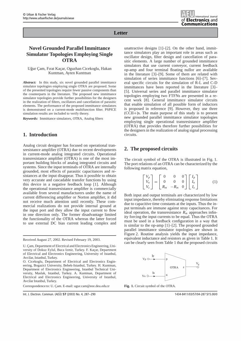
The circuit symbol of the OTRA is illustrated in Fig. 1.The port relations of an OTRA can be characterized by thefollowing matrix equation,
Vp
Vn
Vz
=
0 0 00 0 0
Rm −Rm 0
Ip
In
Iz
(1)
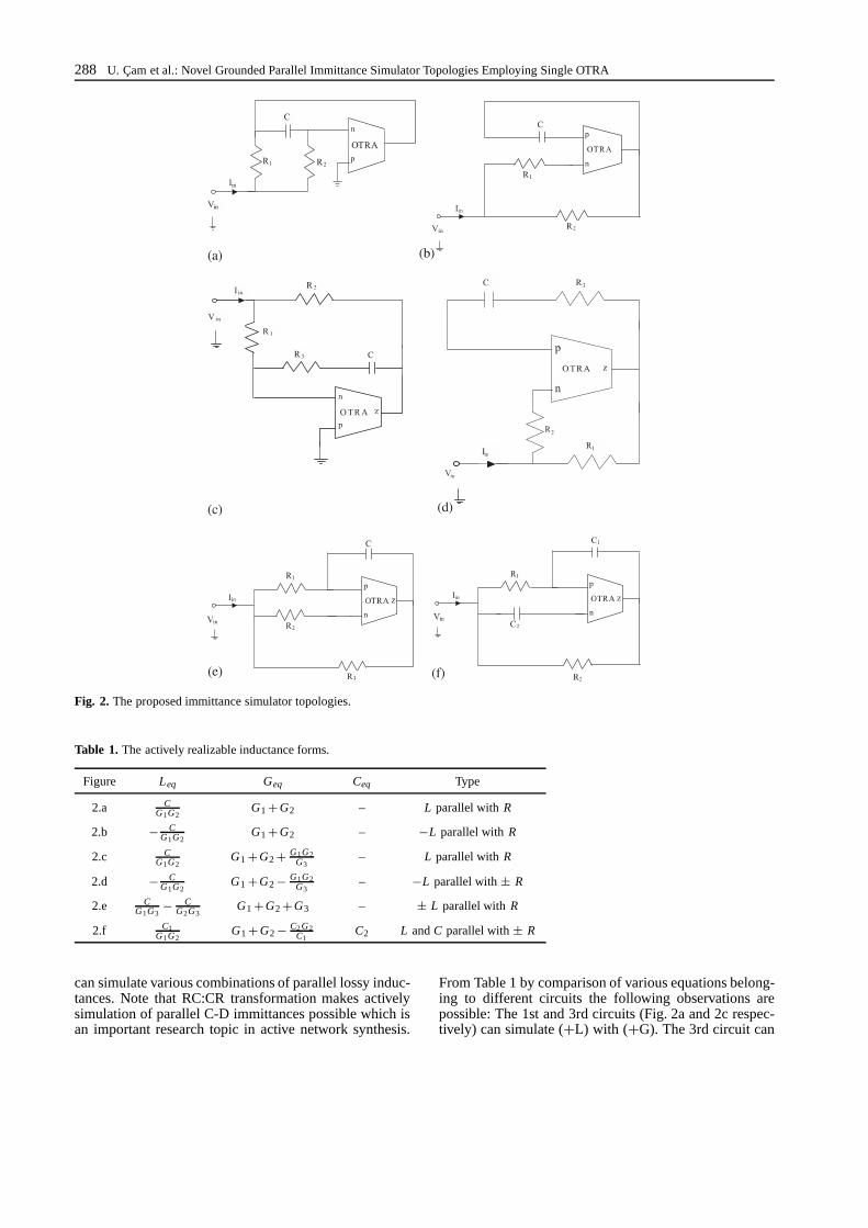
Both input and output terminals are characterized by lowinput impedance, thereby eliminating response limitationsdue to capacitive time constants at the inputs. Thus the in-put terminals are immune against stray capacitances. Forideal operation, the transresistance Rm approaches infin-ity forcing the input currents to be equal. Thus the OTRAmust be used in a feedback configuration in a way thatis similar to the op-amp [1]–[2]. The proposed groundedparallel immittance simulator topologies are shown inFigure 2. Routine analysis yields the input impedance,equivalent inductance and resistors as given in Table 1. Itcan be clearly seen from Table 1 that the proposed circuits
Fig. 1. Circuit symbol of the OTRA.
Int. J. Electron. Commun. (AEU) 57 (2003) No. 4, 287−290 1434-8411/03/57/04-287 $15.00/0
288 U. Çam et al.: Novel Grounded Parallel Immittance Simulator Topologies Employing Single OTRA
Fig. 2. The proposed immittance simulator topologies.
Table 1. The actively realizable inductance forms.
Figure Leq Geq Ceq Type
2.a CG1G2
G1 +G2 – L parallel with R
2.b − CG1G2
G1 +G2 – −L parallel with R
2.c CG1G2
G1 +G2 + G1G2G3
– L parallel with R
2.d − CG1G2
G1 +G2 − G1G2G3
– −L parallel with ± R
2.e CG1G3
− CG2G3
G1 +G2 +G3 – ± L parallel with R
2.f C1G1G2
G1 +G2 − C2 G2C1
C2 L and C parallel with ± R
can simulate various combinations of parallel lossy induc-tances. Note that RC:CR transformation makes activelysimulation of parallel C-D immittances possible which isan important research topic in active network synthesis.
From Table 1 by comparison of various equations belong-ing to different circuits the following observations arepossible: The 1st and 3rd circuits (Fig. 2a and 2c respec-tively) can simulate (+L) with (+G). The 3rd circuit can
U. Çam et al.: Novel Grounded Parallel Immittance Simulator Topologies Employing Single OTRA 289
also simulate (+L) with (+G) providing orthogonal ad-justment of simulated L and G values. It can be used toimplement a current mode filter. The 2nd, 4th and 5th(Fig. 2b, 2d and 2e respectively) can simulate (−L) with(+G). This is especially important if the parasitics have tobe cancelled. The 6th circuit (Fig. 2f) can be useful for thedesign of sinusoidal oscillators since it can simulate (+L),(+C) and (±G).
3. Application example and simulationresults
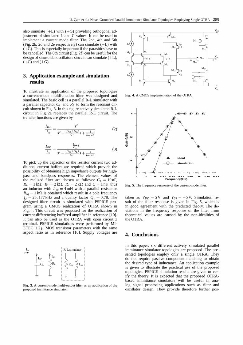
To illustrate an application of the proposed topologiesa current-mode multifunction filter was designed andsimulated. The basic cell is a parallel R-L simulator witha parallel capacitor CL and RL to form the resonant cir-cuit shown in Fig. 3. In this figure actively simulated R-Lcircuit in Fig. 2a replaces the parallel R-L circuit. Thetransfer functions are given by
IHP
Iin= s2
s2 + (Geq+G L )
CLs + 1
LeqCL
(2)
IBP
Iin=
G LCL
s
s2 + (Geq+G L )
CLs + 1
LeqCL
(3)
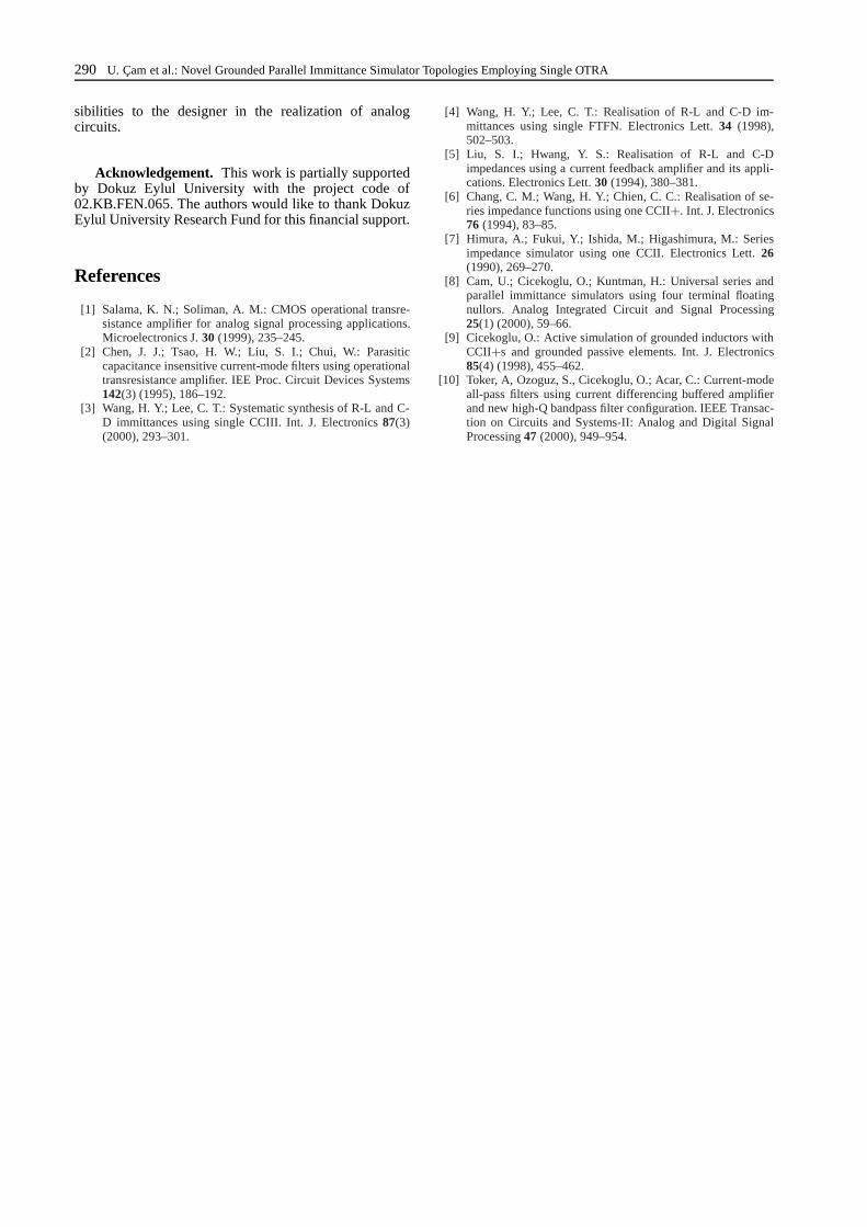
To pick up the capacitor or the resistor current two ad-ditional current buffers are required which provide thepossibility of obtaining high impedance outputs for high-pass and bandpass responses. The element values ofthe realized filter are chosen as follows: CL = 10 nF,RL = 1 kΩ; R1 = 2 kΩ, R2 = 2 kΩ and C = 1 nF, thusan inductor with Leq = 4 mH with a parallel resistanceReq = 1 kΩ is obtained which result in a pole frequencyfp = 25, 177 kHz and a quality factor Qp = 0.78. Thedesigned filter circuit is simulated with PSPICE pro-gram using a CMOS realization of OTRA shown inFig. 4. This circuit was proposed for the realization ofcurrent differencing buffered amplifier in reference [10].It can also be used as the OTRA with open circuit zterminal. PSPICE simulations were performed by MI-ETEC 1.2 µ MOS transistor parameters with the sameaspect ratio as in reference [10]. Supply voltages are
Fig. 3. A current-mode multi-output filter as an application of theproposed immittance simulator.
Fig. 4. A CMOS implementation of the OTRA.
Fig. 5. The frequency response of the current-mode filter.
taken as VDD = 5 V and VSS = −5 V. Simulation re-sult of the filter response is given in Fig. 5, which isin good agreement with the predicted theory. The de-viations in the frequency response of the filter fromtheoretical values are caused by the non-idealities ofthe OTRA.
4. Conclusions
In this paper, six different actively simulated parallelimmittance simulator topologies are proposed. The pre-sented topologies employ only a single OTRA. Theydo not require passive component matching to obtainthe desired type of inductance. An application exampleis given to illustrate the practical use of the proposedtopologies. PSPICE simulation results are given to ver-ify the theory. It is expected that the proposed OTRA-based immittance simulators will be useful in ana-log signal processing applications such as filter andoscillator design. They provide therefore further pos-
290 U. Çam et al.: Novel Grounded Parallel Immittance Simulator Topologies Employing Single OTRA
sibilities to the designer in the realization of analogcircuits.
Acknowledgement. This work is partially supportedby Dokuz Eylul University with the project code of02.KB.FEN.065. The authors would like to thank DokuzEylul University Research Fund for this financial support.
References
[1] Salama, K. N.; Soliman, A. M.: CMOS operational transre-sistance amplifier for analog signal processing applications.Microelectronics J. 30 (1999), 235–245.
[2] Chen, J. J.; Tsao, H. W.; Liu, S. I.; Chui, W.: Parasiticcapacitance insensitive current-mode filters using operationaltransresistance amplifier. IEE Proc. Circuit Devices Systems142(3) (1995), 186–192.
[3] Wang, H. Y.; Lee, C. T.: Systematic synthesis of R-L and C-D immittances using single CCIII. Int. J. Electronics 87(3)(2000), 293–301.
[4] Wang, H. Y.; Lee, C. T.: Realisation of R-L and C-D im-mittances using single FTFN. Electronics Lett. 34 (1998),502–503.
[5] Liu, S. I.; Hwang, Y. S.: Realisation of R-L and C-Dimpedances using a current feedback amplifier and its appli-cations. Electronics Lett. 30 (1994), 380–381.
[6] Chang, C. M.; Wang, H. Y.; Chien, C. C.: Realisation of se-ries impedance functions using one CCII+. Int. J. Electronics76 (1994), 83–85.
[7] Himura, A.; Fukui, Y.; Ishida, M.; Higashimura, M.: Seriesimpedance simulator using one CCII. Electronics Lett. 26(1990), 269–270.
[8] Cam, U.; Cicekoglu, O.; Kuntman, H.: Universal series andparallel immittance simulators using four terminal floatingnullors. Analog Integrated Circuit and Signal Processing25(1) (2000), 59–66.
[9] Cicekoglu, O.: Active simulation of grounded inductors withCCII+s and grounded passive elements. Int. J. Electronics85(4) (1998), 455–462.
[10] Toker, A, Ozoguz, S., Cicekoglu, O.; Acar, C.: Current-modeall-pass filters using current differencing buffered amplifierand new high-Q bandpass filter configuration. IEEE Transac-tion on Circuits and Systems-II: Analog and Digital SignalProcessing 47 (2000), 949–954.