Embed Size (px)
Citation preview
FN6436Rev 0.00
June 18, 2007
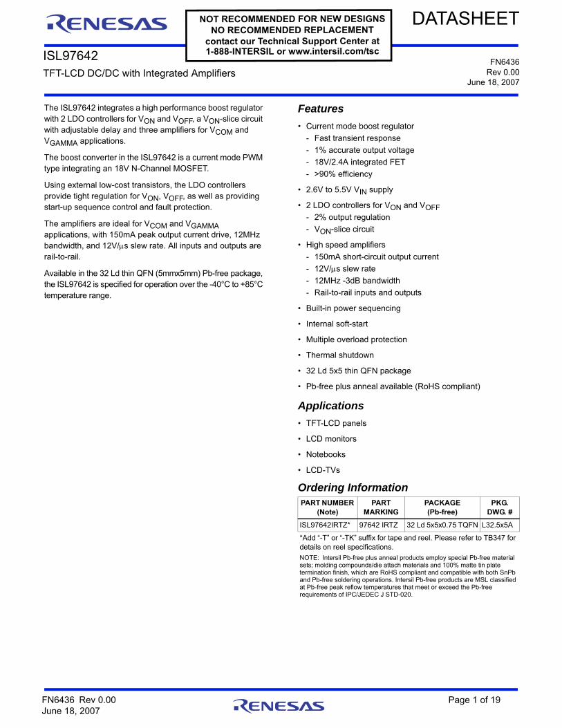
ISL97642TFT-LCD DC/DC with Integrated Amplifiers
DATASHEETNOT RECOMMENDED FOR NEW DESIGNSNO RECOMMENDED REPLACEMENT
contact our Technical Support Center at1-888-INTERSIL or www.intersil.com/tsc
The ISL97642 integrates a high performance boost regulator with 2 LDO controllers for VON and VOFF, a VON-slice circuit with adjustable delay and three amplifiers for VCOM and VGAMMA applications.
The boost converter in the ISL97642 is a current mode PWM type integrating an 18V N-Channel MOSFET.
Using external low-cost transistors, the LDO controllers provide tight regulation for VON, VOFF, as well as providing start-up sequence control and fault protection.
The amplifiers are ideal for VCOM and VGAMMA applications, with 150mA peak output current drive, 12MHz bandwidth, and 12V/s slew rate. All inputs and outputs are rail-to-rail.
Available in the 32 Ld thin QFN (5mmx5mm) Pb-free package, the ISL97642 is specified for operation over the -40°C to +85°C temperature range.
Features
• Current mode boost regulator
- Fast transient response
- 1% accurate output voltage
- 18V/2.4A integrated FET
- >90% efficiency
• 2.6V to 5.5V VIN supply
• 2 LDO controllers for VON and VOFF- 2% output regulation
- VON-slice circuit
• High speed amplifiers
- 150mA short-circuit output current
- 12V/s slew rate
- 12MHz -3dB bandwidth
- Rail-to-rail inputs and outputs
• Built-in power sequencing
• Internal soft-start
• Multiple overload protection
• Thermal shutdown
• 32 Ld 5x5 thin QFN package
• Pb-free plus anneal available (RoHS compliant)
Applications
• TFT-LCD panels
• LCD monitors
• Notebooks
• LCD-TVs
Ordering InformationPART NUMBER
(Note)PART
MARKINGPACKAGE (Pb-free)
PKG. DWG. #
ISL97642IRTZ* 97642 IRTZ 32 Ld 5x5x0.75 TQFN L32.5x5A
*Add “-T” or “-TK” suffix for tape and reel. Please refer to TB347 for details on reel specifications.
NOTE: Intersil Pb-free plus anneal products employ special Pb-free material sets; molding compounds/die attach materials and 100% matte tin plate termination finish, which are RoHS compliant and compatible with both SnPb and Pb-free soldering operations. Intersil Pb-free products are MSL classified at Pb-free peak reflow temperatures that meet or exceed the Pb-free requirements of IPC/JEDEC J STD-020.
FN6436 Rev 0.00 Page 1 of 19June 18, 2007
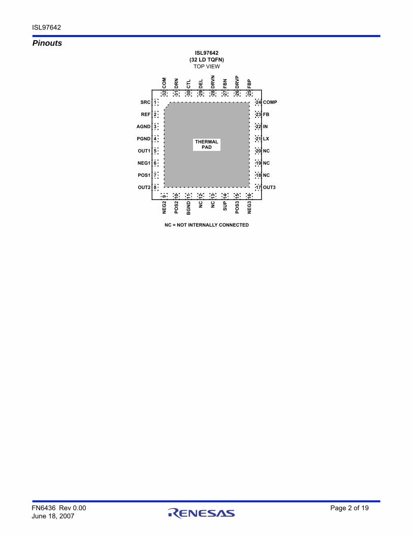
ISL97642
PinoutsISL97642
(32 LD TQFN)TOP VIEW
NC = NOT INTERNALLY CONNECTED
THERMAL PAD
24
23
22
21
20
19
18
32
31
30
29
28
10
11
12
13
14
1
2
3
4
5
6
7
8 17
15
27
16
26
9
25
SRC
REF
AGND
PGND
OUT1
NEG1
POS1
OUT2
NE
G2
PO
S2
BG
ND
NC
NC
SU
P
PO
S3
NE
G3
COMP
FB
IN
LX
NC
NC
NC
OUT3
FB
P
CO
M
DR
N
CT
L
DE
L
DR
VN
FB
N
DR
VP
FN6436 Rev 0.00 Page 2 of 19June 18, 2007
ISL97642
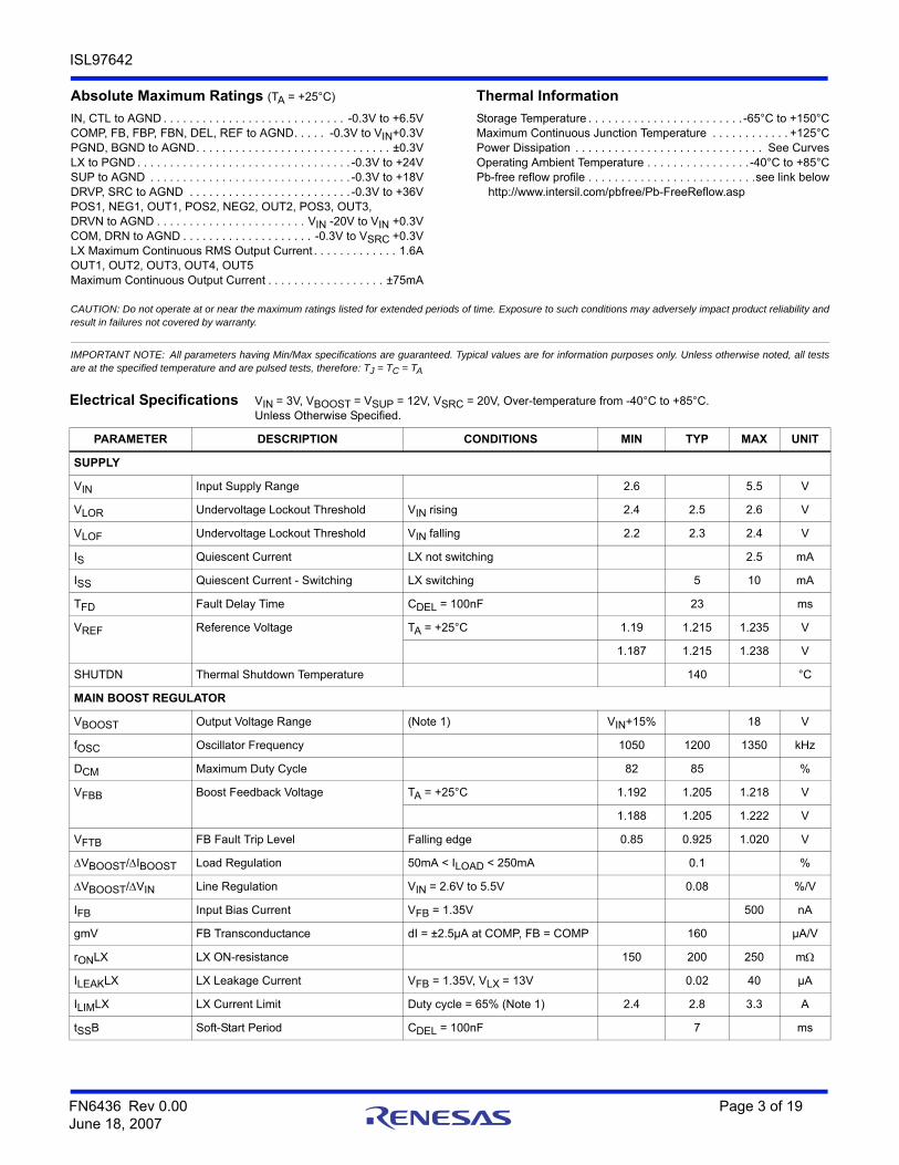
Absolute Maximum Ratings (TA = +25°C) Thermal Information
IN, CTL to AGND . . . . . . . . . . . . . . . . . . . . . . . . . . . . -0.3V to +6.5VCOMP, FB, FBP, FBN, DEL, REF to AGND. . . . . -0.3V to VIN+0.3VPGND, BGND to AGND. . . . . . . . . . . . . . . . . . . . . . . . . . . . . . ±0.3VLX to PGND . . . . . . . . . . . . . . . . . . . . . . . . . . . . . . . . . -0.3V to +24VSUP to AGND . . . . . . . . . . . . . . . . . . . . . . . . . . . . . . . -0.3V to +18VDRVP, SRC to AGND . . . . . . . . . . . . . . . . . . . . . . . . . -0.3V to +36VPOS1, NEG1, OUT1, POS2, NEG2, OUT2, POS3, OUT3, DRVN to AGND . . . . . . . . . . . . . . . . . . . . . . . VIN -20V to VIN +0.3VCOM, DRN to AGND . . . . . . . . . . . . . . . . . . . . -0.3V to VSRC +0.3VLX Maximum Continuous RMS Output Current . . . . . . . . . . . . . 1.6AOUT1, OUT2, OUT3, OUT4, OUT5 Maximum Continuous Output Current . . . . . . . . . . . . . . . . . . ±75mA
Storage Temperature . . . . . . . . . . . . . . . . . . . . . . . . -65°C to +150°CMaximum Continuous Junction Temperature . . . . . . . . . . . . +125°CPower Dissipation . . . . . . . . . . . . . . . . . . . . . . . . . . . . . See CurvesOperating Ambient Temperature . . . . . . . . . . . . . . . . -40°C to +85°CPb-free reflow profile . . . . . . . . . . . . . . . . . . . . . . . . . .see link below
http://www.intersil.com/pbfree/Pb-FreeReflow.asp
CAUTION: Do not operate at or near the maximum ratings listed for extended periods of time. Exposure to such conditions may adversely impact product reliability andresult in failures not covered by warranty.
IMPORTANT NOTE: All parameters having Min/Max specifications are guaranteed. Typical values are for information purposes only. Unless otherwise noted, all testsare at the specified temperature and are pulsed tests, therefore: TJ = TC = TA
Electrical Specifications VIN = 3V, VBOOST = VSUP = 12V, VSRC = 20V, Over-temperature from -40°C to +85°C.Unless Otherwise Specified.
PARAMETER DESCRIPTION CONDITIONS MIN TYP MAX UNIT
SUPPLY
VIN Input Supply Range 2.6 5.5 V
VLOR Undervoltage Lockout Threshold VIN rising 2.4 2.5 2.6 V
VLOF Undervoltage Lockout Threshold VIN falling 2.2 2.3 2.4 V
IS Quiescent Current LX not switching 2.5 mA
ISS Quiescent Current - Switching LX switching 5 10 mA
TFD Fault Delay Time CDEL = 100nF 23 ms
VREF Reference Voltage TA = +25°C 1.19 1.215 1.235 V
1.187 1.215 1.238 V
SHUTDN Thermal Shutdown Temperature 140 °C
MAIN BOOST REGULATOR
VBOOST Output Voltage Range (Note 1) VIN+15% 18 V
fOSC Oscillator Frequency 1050 1200 1350 kHz
DCM Maximum Duty Cycle 82 85 %
VFBB Boost Feedback Voltage TA = +25°C 1.192 1.205 1.218 V
1.188 1.205 1.222 V
VFTB FB Fault Trip Level Falling edge 0.85 0.925 1.020 V
VBOOST/IBOOST Load Regulation 50mA < ILOAD < 250mA 0.1 %
VBOOST/VIN Line Regulation VIN = 2.6V to 5.5V 0.08 %/V
IFB Input Bias Current VFB = 1.35V 500 nA
gmV FB Transconductance dI = ±2.5µA at COMP, FB = COMP 160 µA/V
rONLX LX ON-resistance 150 200 250 m
ILEAKLX LX Leakage Current VFB = 1.35V, VLX = 13V 0.02 40 µA
ILIMLX LX Current Limit Duty cycle = 65% (Note 1) 2.4 2.8 3.3 A
tSSB Soft-Start Period CDEL = 100nF 7 ms
FN6436 Rev 0.00 Page 3 of 19June 18, 2007
ISL97642
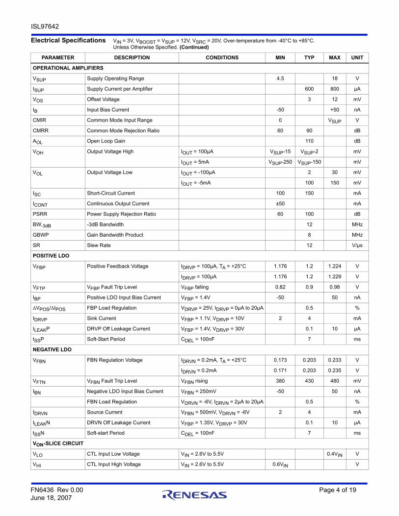
OPERATIONAL AMPLIFIERS
VSUP Supply Operating Range 4.5 18 V
ISUP Supply Current per Amplifier 600 800 µA
VOS Offset Voltage 3 12 mV
IB Input Bias Current -50 +50 nA
CMIR Common Mode Input Range 0 VSUP V
CMRR Common Mode Rejection Ratio 60 90 dB
AOL Open Loop Gain 110 dB
VOH Output Voltage High IOUT = 100µA VSUP-15 VSUP-2 mV
IOUT = 5mA VSUP-250 VSUP-150 mV
VOL Output Voltage Low IOUT = -100µA 2 30 mV
IOUT = -5mA 100 150 mV
ISC Short-Circuit Current 100 150 mA
ICONT Continuous Output Current ±50 mA
PSRR Power Supply Rejection Ratio 60 100 dB
BW-3dB -3dB Bandwidth 12 MHz
GBWP Gain Bandwidth Product 8 MHz
SR Slew Rate 12 V/µs
POSITIVE LDO
VFBP Positive Feedback Voltage IDRVP = 100µA, TA = +25°C 1.176 1.2 1.224 V
IDRVP = 100µA 1.176 1.2 1.229 V
VFTP VFBP Fault Trip Level VFBP falling 0.82 0.9 0.98 V
IBP Positive LDO Input Bias Current VFBP = 1.4V -50 50 nA
VPOS/IPOS FBP Load Regulation VDRVP = 25V, IDRVP = 0µA to 20µA 0.5 %
IDRVP Sink Current VFBP = 1.1V, VDRVP = 10V 2 4 mA
ILEAKP DRVP Off Leakage Current VFBP = 1.4V, VDRVP = 30V 0.1 10 µA
tSSP Soft-Start Period CDEL = 100nF 7 ms
NEGATIVE LDO
VFBN FBN Regulation Voltage IDRVN = 0.2mA, TA = +25°C 0.173 0.203 0.233 V
IDRVN = 0.2mA 0.171 0.203 0.235 V
VFTN VFBN Fault Trip Level VFBN rising 380 430 480 mV
IBN Negative LDO Input Bias Current VFBN = 250mV -50 50 nA
FBN Load Regulation VDRVN = -6V, IDRVN = 2µA to 20µA 0.5 %
IDRVN Source Current VFBN = 500mV, VDRVN = -6V 2 4 mA
ILEAKN DRVN Off Leakage Current VFBP = 1.35V, VDRVP = 30V 0.1 10 µA
tSSN Soft-start Period CDEL = 100nF 7 ms
VON-SLICE CIRCUIT
VLO CTL Input Low Voltage VIN = 2.6V to 5.5V 0.4VIN V
VHI CTL Input High Voltage VIN = 2.6V to 5.5V 0.6VIN V
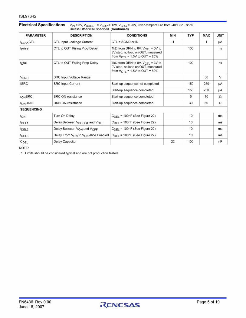
Electrical Specifications VIN = 3V, VBOOST = VSUP = 12V, VSRC = 20V, Over-temperature from -40°C to +85°C.Unless Otherwise Specified. (Continued)
PARAMETER DESCRIPTION CONDITIONS MIN TYP MAX UNIT
FN6436 Rev 0.00 Page 4 of 19June 18, 2007
ISL97642
ILEAKCTL CTL Input Leakage Current CTL = AGND or IN -1 1 µA
tDrise CTL to OUT Rising Prop Delay 1k from DRN to 8V, VCTL = 0V to 3V step, no load on OUT, measured from VCTL = 1.5V to OUT = 20%
100 ns
tDfall CTL to OUT Falling Prop Delay 1k from DRN to 8V, VCTL = 3V to 0V step, no load on OUT, measured from VCTL = 1.5V to OUT = 80%
100 ns
VSRC SRC Input Voltage Range 30 V
ISRC SRC Input Current Start-up sequence not completed 150 250 µA
Start-up sequence completed 150 250 µA
rONSRC SRC ON-resistance Start-up sequence completed 5 10
rONDRN DRN ON-resistance Start-up sequence completed 30 60
SEQUENCING
tON Turn On Delay CDEL = 100nF (See Figure 22) 10 ms
tDEL1 Delay Between VBOOST and VOFF CDEL = 100nF (See Figure 22) 10 ms
tDEL2 Delay Between VON and VOFF CDEL = 100nF (See Figure 22) 10 ms
tDEL3 Delay From VON to VON-slice Enabled CDEL = 100nF (See Figure 22) 10 ms
CDEL Delay Capacitor 22 100 nF
NOTE:
1. Limits should be considered typical and are not production tested.
Electrical Specifications VIN = 3V, VBOOST = VSUP = 12V, VSRC = 20V, Over-temperature from -40°C to +85°C.Unless Otherwise Specified. (Continued)
PARAMETER DESCRIPTION CONDITIONS MIN TYP MAX UNIT
FN6436 Rev 0.00 Page 5 of 19June 18, 2007
ISL97642
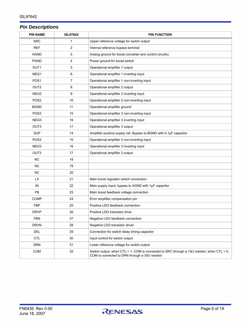
Pin Descriptions
PIN NAME ISL97642 PIN FUNCTION
SRC 1 Upper reference voltage for switch output
REF 2 Internal reference bypass terminal
AGND 3 Analog ground for boost converter and control circuitry
PGND 4 Power ground for boost switch
OUT1 5 Operational amplifier 1 output
NEG1 6 Operational amplifier 1 inverting input
POS1 7 Operational amplifier 1 non-inverting input
OUT2 8 Operational amplifier 2 output
NEG2 9 Operational amplifier 2 inverting input
POS2 10 Operational amplifier 2 non-inverting input
BGND 11 Operational amplifier ground
POS3 15 Operational amplifier 3 non-inverting input
NEG3 16 Operational amplifier 3 inverting input
OUT3 17 Operational amplifier 3 output
SUP 14 Amplifier positive supply rail. Bypass to BGND with 0.1µF capacitor
POS3 15 Operational amplifier 3 non-inverting input
NEG3 16 Operational amplifier 3 inverting input
OUT3 17 Operational amplifier 3 output
NC 18
NC 19
NC 20
LX 21 Main boost regulator switch connection
IN 22 Main supply input; bypass to AGND with 1µF capacitor
FB 23 Main boost feedback voltage connection
COMP 24 Error amplifier compensation pin
FBP 25 Positive LDO feedback connection
DRVP 26 Positive LDO transistor drive
FBN 27 Negative LDO feedback connection
DRVN 28 Negative LDO transistor driver
DEL 29 Connection for switch delay timing capacitor
CTL 30 Input control for switch output
DRN 31 Lower reference voltage for switch output
COM 32 Switch output; when CTL = 1, COM is connected to SRC through a 15 resistor; when CTL = 0, COM is connected to DRN through a 30 resistor
FN6436 Rev 0.00 Page 6 of 19June 18, 2007
ISL97642 ISL97642
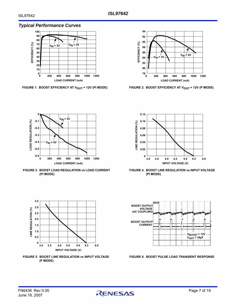
Typical Performance Curves
FIGURE 1. BOOST EFFICIENCY AT VOUT = 12V (PI MODE) FIGURE 2. BOOST EFFICIENCY AT VOUT = 12V (P MODE)
FIGURE 3. BOOST LOAD REGULATION vs LOAD CURRENT (PI MODE)
FIGURE 4. BOOST LINE REGULATION vs INPUT VOLTAGE (PI MODE)
FIGURE 5. BOOST LINE REGULATION vs INPUT VOLTAGE(P MODE)
FIGURE 6. BOOST PULSE LOAD TRANSIENT RESPONSE
0
10
20
30
40
50
60
70
80
90
100E
FF
ICIE
NC
Y (
%)
0 200 400 600 800 1000 1200
LOAD CURRENT (mA)
VIN = 3V VIN = 5V
EF
FIC
IEN
CY
(%
)
78
80
82
84
86
88
90
92
94
0 200 400 600 800 1000 1200
LOAD CURRENT (mA)
VIN = 5VVIN = 3V
LO
AD
RE
GU
LA
TIO
N (
%)
-0.6
-0.5
-0.4
-0.3
-0.2
-0.1
0
0 200 400 600 800 1000 1200
LOAD CURRENT (mA)
VIN = 5V
VIN = 3V
0
0.02
0.04
0.06
0.08
0.10
0.12
3.0 3.5 4.0 4.5 5.0 5.5 6.0
INPUT VOLTAGE (V)
LIN
E R
EG
UL
AT
ION
(%
)
0.5
0
1.0
1.5
2.0
2.5
3.5
3.0 3.5 4.0 4.5 5.0 5.5 6.0
INPUT VOLTAGE (V)
LIN
E R
EG
UL
AT
ION
(%
) 3.0BOOST OUTPUT
(AC COUPLING)
VBOOST = 12VCOUT = 30µF
VOLTAGE
BOOST OUTPUTCURRENT
FN6436 Rev 0.00 Page 7 of 19June 18, 2007
ISL97642
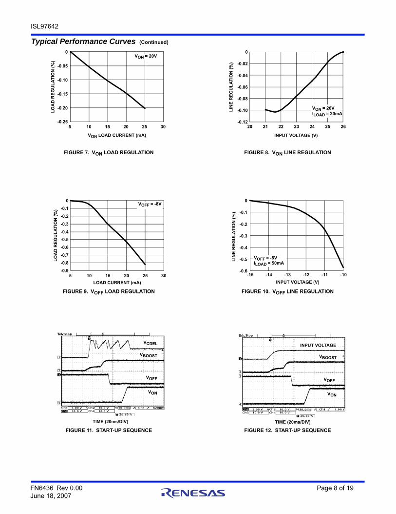
FIGURE 7. VON LOAD REGULATION FIGURE 8. VON LINE REGULATION
FIGURE 9. VOFF LOAD REGULATION FIGURE 10. VOFF LINE REGULATION
FIGURE 11. START-UP SEQUENCE FIGURE 12. START-UP SEQUENCE
Typical Performance Curves (Continued)
-0.25
-0.20
-0.15
-0.10
-0.05
0
5 10 15 20 25 30
VON LOAD CURRENT (mA)
LO
AD
RE
GU
LA
TIO
N (
%)
VON = 20V
-0.12
-0.10
-0.08
-0.06
-0.04
-0.02
0
20 21 22 23 24 25 26
INPUT VOLTAGE (V)
LIN
E R
EG
UL
AT
ION
(%
)
VON = 20VILOAD = 20mA
-0.9
-0.8
-0.7
-0.6
-0.5
-0.4
-0.3
-0.2
-0.1
0
5 10 15 20 25 30
LOAD CURRENT (mA)
LO
AD
RE
GU
LA
TIO
N (
%)
VOFF = -8V
-0.6
-0.5
-0.4
-0.3
-0.2
-0.1
0
-15 -14 -13 -12 -11 -10
INPUT VOLTAGE (V)
LIN
E R
EG
UL
AT
ION
(%
)
VOFF = -8VILOAD = 50mA
TIME (20ms/DIV)
VCDEL
VBOOST
VOFF
VON
TIME (20ms/DIV)
INPUT VOLTAGE
VBOOST
VOFF
VON
FN6436 Rev 0.00 Page 8 of 19June 18, 2007
ISL97642
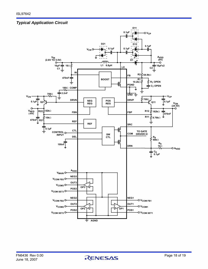
Applications InformationThe ISL97642 provides a highly integrated multiple output power solution for TFT-LCD applications. The system consists of one high efficiency boost converter and two low cost linear-regulator controllers (VON and VOFF) with multiple protection functions. The block diagram of the whole part is shown in Figure 16. Table 1 lists the recommended components.
The ISL97642 integrates an N-Channel MOSFET in boost converter to minimize the external component counts and cost. The VON, VOFF linear-regulators are independently regulated by using external resistors. To achieve higher voltage than VBOOST, one or multiple stage charge pumps may be used.
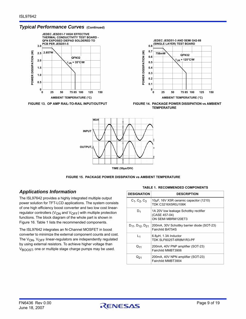
FIGURE 13. OP AMP RAIL-TO-RAIL INPUT/OUTPUT FIGURE 14. PACKAGE POWER DISSIPATION vs AMBIENT TEMPERATURE
FIGURE 15. PACKAGE POWER DISSIPATION vs AMBIENT TEMPERATURE
Typical Performance Curves (Continued)
JEDEC JESD51-7 HIGH EFFECTIVE THERMAL CONDUCTIVITY TEST BOARD - QFN EXPOSED DIEPAD SOLDERED TO PCB PER JESD51-5
3.0
2.5
2.0
1.5
1.0
0.5
00 25 50 75 100 150
AMBIENT TEMPERATURE (°C)
PO
WE
R D
ISS
IPA
TIO
N (
W)
2.857W
JA = 35°C/W
QFN32
12585
JEDEC JESD51-3 AND SEMI G42-88 (SINGLE LAYER) TEST BOARD
0.8
0.7
0.5
0.3
0.2
0.1
00 25 50 75 100 150
AMBIENT TEMPERATURE (°C)
PO
WE
R D
ISS
IPA
TIO
N (
W)
12585
0.6
0.4
JA = 125°C/W
QFN32758mW
INPUT
OUTPUT
TIME (50µs/DIV)
TABLE 1. RECOMMENDED COMPONENTS
DESIGNATION DESCRIPTION
C1, C2, C3 10µF, 16V X5R ceramic capacitor (1210)TDK C3216X5R0J106K
D1 1A 20V low leakage Schottky rectifier (CASE 457-04)ON SEMI MBRM120ET3
D11, D12, D21 200mA, 30V Schottky barrier diode (SOT-23)Fairchild BAT54S
L1 6.8µH, 1.3A InductorTDK SLF6025T-6R8M1R3-PF
Q11 200mA, 40V PNP amplifier (SOT-23)Fairchild MMBT3906
Q21 200mA, 40V NPN amplifier (SOT-23)Fairchild MMBT3904
FN6436 Rev 0.00 Page 9 of 19June 18, 2007
ISL97642
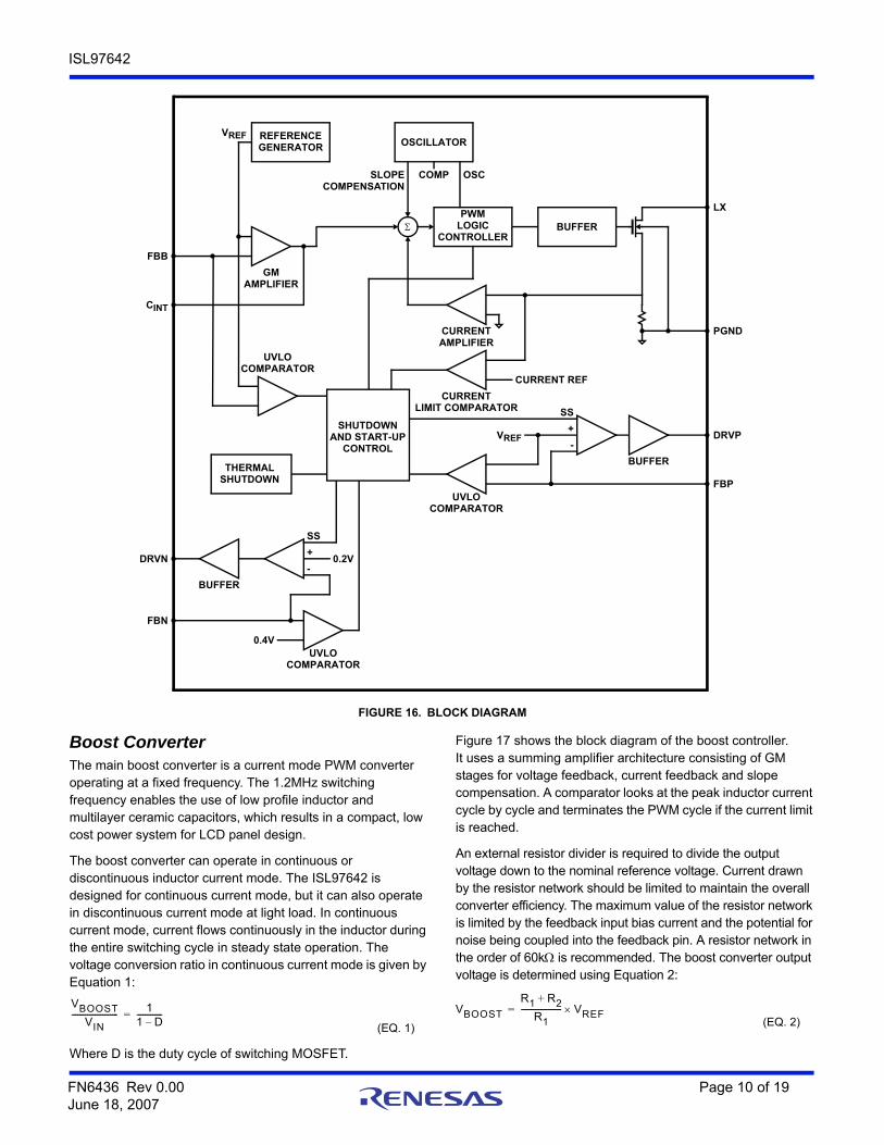
FIGURE 16. BLOCK DIAGRAM
Boost ConverterThe main boost converter is a current mode PWM converter operating at a fixed frequency. The 1.2MHz switching frequency enables the use of low profile inductor and multilayer ceramic capacitors, which results in a compact, low cost power system for LCD panel design.
The boost converter can operate in continuous or discontinuous inductor current mode. The ISL97642 is designed for continuous current mode, but it can also operate in discontinuous current mode at light load. In continuous current mode, current flows continuously in the inductor during the entire switching cycle in steady state operation. The voltage conversion ratio in continuous current mode is given by Equation 1:
Where D is the duty cycle of switching MOSFET.
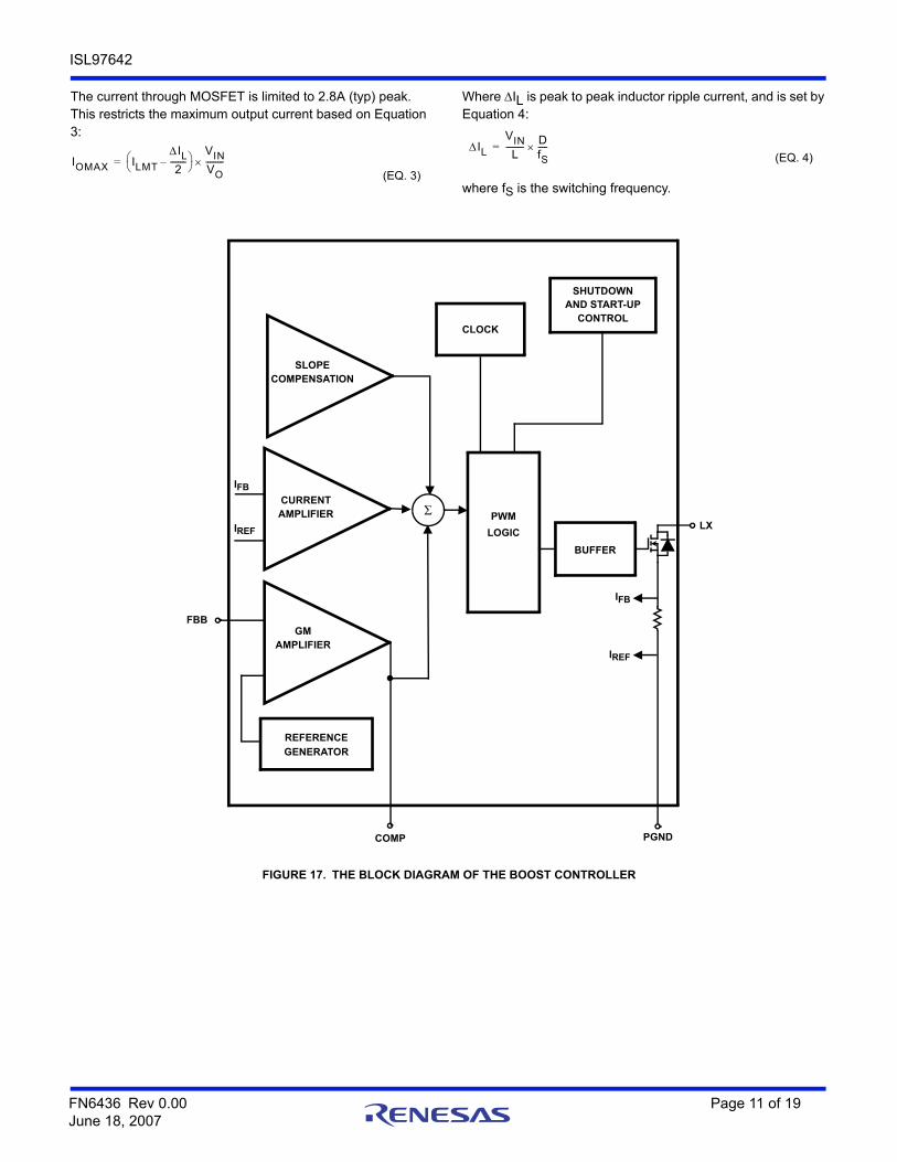
Figure 17 shows the block diagram of the boost controller. It uses a summing amplifier architecture consisting of GM stages for voltage feedback, current feedback and slope compensation. A comparator looks at the peak inductor current cycle by cycle and terminates the PWM cycle if the current limit is reached.
An external resistor divider is required to divide the output voltage down to the nominal reference voltage. Current drawn by the resistor network should be limited to maintain the overall converter efficiency. The maximum value of the resistor network is limited by the feedback input bias current and the potential for noise being coupled into the feedback pin. A resistor network in the order of 60k is recommended. The boost converter output voltage is determined using Equation 2:
PWM
LOGICCONTROLLER
BUFFER
OSCILLATOR
SLOPECOMPENSATION
OSC
REFERENCEGENERATOR
VREF
GMAMPLIFIER
UVLOCOMPARATOR
CURRENTAMPLIFIER
THERMALSHUTDOWN
SS
+
-
UVLOCOMPARATOR
BUFFER
UVLOCOMPARATOR
SS
+
-
SHUTDOWNAND START-UP
CONTROLBUFFER
FBP
DRVP
FBB
CINT
DRVN
FBN
0.4V
0.2V
VREF
COMP
CURRENTLIMIT COMPARATOR
CURRENT REF
PGND
LX
VBOOSTVIN
------------------------ 11 D–-------------=
(EQ. 1)
VBOOST
R1 R2+
R1--------------------- VREF=
(EQ. 2)
FN6436 Rev 0.00 Page 10 of 19June 18, 2007
ISL97642
The current through MOSFET is limited to 2.8A (typ) peak. This restricts the maximum output current based on Equation 3:
Where IL is peak to peak inductor ripple current, and is set by Equation 4:
where fS is the switching frequency.
FIGURE 17. THE BLOCK DIAGRAM OF THE BOOST CONTROLLER
IOMAX ILMT
IL2--------–
VINVO---------=
(EQ. 3)
ILVINL--------- D
fS-----=
(EQ. 4)
IREF
IREF
FBB
IFB
IFB
COMP
LX
PGND
SHUTDOWNAND START-UP
CONTROL
GM AMPLIFIER
SLOPE COMPENSATION
BUFFER
PWM
LOGIC
CURRENT AMPLIFIER
CLOCK
REFERENCE
GENERATOR
FN6436 Rev 0.00 Page 11 of 19June 18, 2007
ISL97642
Table 2 gives typical values (margins are considered 10%, 3%, 20%, 10% and 15% on VIN, VO, L, fS and ILMT:
Input Capacitor
The input capacitor is used to supply the current to the converter. It is recommended that CIN be larger than 10F. The reflected ripple voltage will be smaller with larger CIN. The voltage rating of input capacitor should be larger than the maximum input voltage.
Boost Inductor
The boost inductor is a critical part which influences the output voltage ripple, transient response, and efficiency. Value of 3.3H to 10H inductor is recommended in applications to fit the internal slope compensation. The inductor must be able to handle the following average and peak current:
Rectifier DiodeA high-speed diode is desired due to the high switching frequency. Schottky diodes are recommended because of their fast recovery time and low forward voltage. The rectifier diode must meet the output current and peak inductor current requirements.
Output CapacitorThe output capacitor supplies the load directly and reduces the ripple voltage at the output. Output ripple voltage consists of two components: the voltage drop due to the inductor ripple current flowing through the ESR of output capacitor, and the charging and discharging of the output capacitor.
For low ESR ceramic capacitors, the output ripple is dominated by the charging and discharging of the output capacitor. The voltage rating of the output capacitor should be greater than the maximum output voltage.
NOTE: Capacitors have a voltage coefficient that makes their effective capacitance drop as the voltage across them increases. COUT in the
Equation 6 assumes the effective value of the capacitor at a particular voltage and not the manufacturer’s stated value, measured at zero volts.
Compensation
The ISL97642 incorporates a transconductance amplifier in its feedback path to allow the user some adjustment on the transient response and better regulation. The ISL97642 uses current mode control architecture, which has a fast current sense loop and a slow voltage feedback loop. The fast current feedback loop does not require any compensation. The slow voltage loop must be compensated for stable operation. The compensation network is a series RC network from COMP pin to ground. The resistor sets the high frequency integrator gain for fast transient response and the capacitor sets the integrator zero to ensure loop stability. For most applications, a 2.2nF capacitor and a 180 resistor are inserted in series between COMP pin and ground. To improve the transient response, either the resistor value can be increased or the capacitor value can be reduced, but too high resistor value or too low capacitor value will reduce loop stability.
Boost Feedback Resistors
As the boost output voltage, VBOOST, is reduced below 12V, the effective voltage feedback in the IC increases the ratio of voltage to current feedback at the summing comparator because R2 decreases relative to R1. To maintain stable operation over the complete current range of the IC, the voltage feedback to the FBB pin should be reduced proportionally (as VBOOST is reduced) by means of a series resistor-capacitor network (R7 and C7) in parallel with R1, with a pole frequency (fp) set to approximately 10kHz for C2 (effective) = 10µF and 4kHz for C2 (effective) = 30µF.
Linear-Regulator Controllers (VON and VOFF)
The ISL97642 includes 2 independent linear-regulator controllers, in which there is one positive output voltage (VON) and one negative voltage (VOFF). The VON and VOFF linear-regulator controller function diagram, application circuit and waveforms are shown in Figures 18 and 19 respectively.
TABLE 2.
VIN (V) VO (V) L (µH) fS (MHz) IOMAX (mA)
3.3 9 6.8 1.2 890
3.3 12 6.8 1.2 666
3.3 15 6.8 1.2 530
5 9 6.8 1.2 1350
5 12 6.8 1.2 1000
5 15 6.8 1.2 795
ILAVG
IO1 D–-------------= (EQ. 5)
ILPK ILAVG
IL2--------+=
VRIPPLE ILPK ESRVO VIN–
VO------------------------
IOCOUT---------------- 1
fS-----+=
(EQ. 6)
R7 1 0.1 R2 1 R1 ^-1–= (EQ. 7)
C7 1 2 3.142 fp R7= (EQ. 8)
FN6436 Rev 0.00 Page 12 of 19June 18, 2007
ISL97642
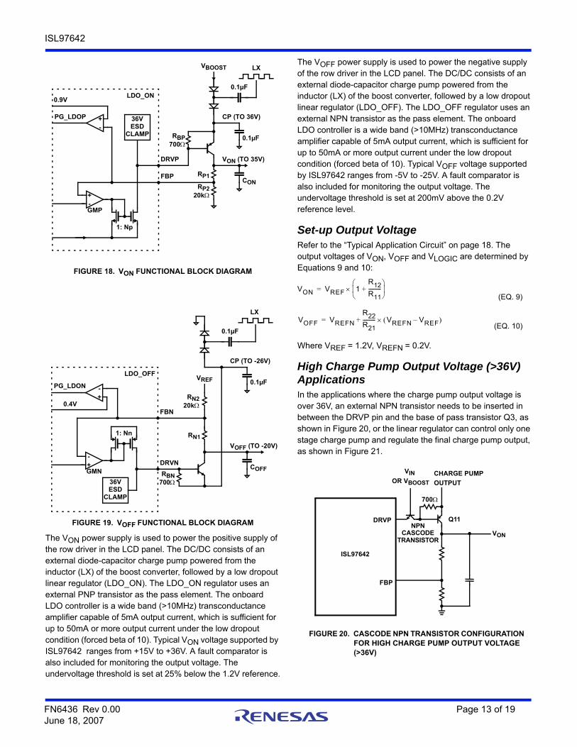
The VON power supply is used to power the positive supply of the row driver in the LCD panel. The DC/DC consists of an external diode-capacitor charge pump powered from the inductor (LX) of the boost converter, followed by a low dropout linear regulator (LDO_ON). The LDO_ON regulator uses an external PNP transistor as the pass element. The onboard LDO controller is a wide band (>10MHz) transconductance amplifier capable of 5mA output current, which is sufficient for up to 50mA or more output current under the low dropout condition (forced beta of 10). Typical VON voltage supported by ISL97642 ranges from +15V to +36V. A fault comparator is also included for monitoring the output voltage. The undervoltage threshold is set at 25% below the 1.2V reference.
The VOFF power supply is used to power the negative supply of the row driver in the LCD panel. The DC/DC consists of an external diode-capacitor charge pump powered from the inductor (LX) of the boost converter, followed by a low dropout linear regulator (LDO_OFF). The LDO_OFF regulator uses an external NPN transistor as the pass element. The onboard LDO controller is a wide band (>10MHz) transconductance amplifier capable of 5mA output current, which is sufficient for up to 50mA or more output current under the low dropout condition (forced beta of 10). Typical VOFF voltage supported by ISL97642 ranges from -5V to -25V. A fault comparator is also included for monitoring the output voltage. The undervoltage threshold is set at 200mV above the 0.2V reference level.
Set-up Output VoltageRefer to the “Typical Application Circuit” on page 18. The output voltages of VON, VOFF and VLOGIC are determined by Equations 9 and 10:
Where VREF = 1.2V, VREFN = 0.2V.
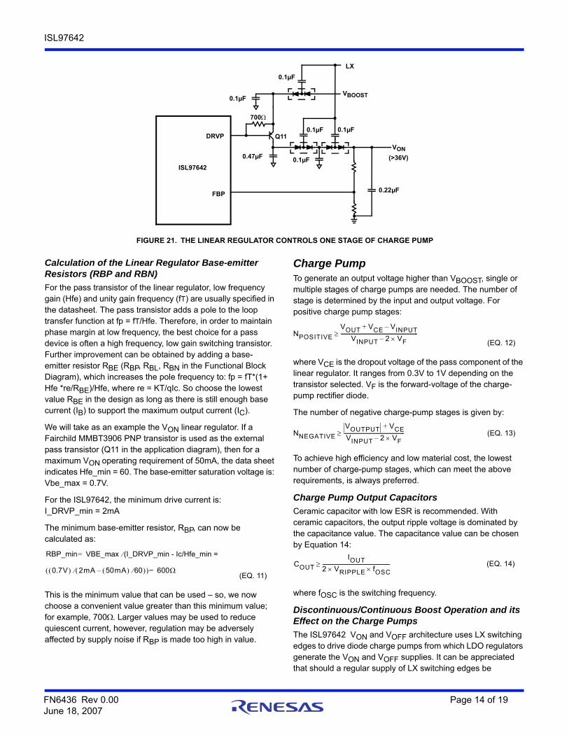
High Charge Pump Output Voltage (>36V) ApplicationsIn the applications where the charge pump output voltage is over 36V, an external NPN transistor needs to be inserted in between the DRVP pin and the base of pass transistor Q3, as shown in Figure 20, or the linear regulator can control only one stage charge pump and regulate the final charge pump output, as shown in Figure 21.
-+
-+ 36V
ESDCLAMP
GMP
LDO_ON
PG_LDOP
1: Np
FBP
DRVP
700RBP
VBOOST
0.1µF
0.1µF
CP (TO 36V)
20kRP2
RP1CON
VON (TO 35V)
LX
0.9V
FIGURE 18. VON FUNCTIONAL BLOCK DIAGRAM
-+
-+
36VESD
CLAMP
GMN
LDO_OFF
1: Nn
FBN
DRVN
0.1µF
0.1µF
CP (TO -26V)
RBN
COFF
VOFF (TO -20V)
LX
RN1
RN220k
VREFPG_LDON
0.4V
700
FIGURE 19. VOFF FUNCTIONAL BLOCK DIAGRAM
VON VREF 1R12R11----------+
=(EQ. 9)
VOFF VREFN
R22R21---------- VREFN VREF– +=
(EQ. 10)
VIN
OR VBOOST
CHARGE PUMP
OUTPUT
700
Q11
FBP
DRVP NPN
CASCODE TRANSISTOR
ISL97642
VON
FIGURE 20. CASCODE NPN TRANSISTOR CONFIGURATION FOR HIGH CHARGE PUMP OUTPUT VOLTAGE (>36V)
FN6436 Rev 0.00 Page 13 of 19June 18, 2007
ISL97642
Calculation of the Linear Regulator Base-emitter Resistors (RBP and RBN)
For the pass transistor of the linear regulator, low frequency gain (Hfe) and unity gain frequency (fT) are usually specified in the datasheet. The pass transistor adds a pole to the loop transfer function at fp = fT/Hfe. Therefore, in order to maintain phase margin at low frequency, the best choice for a pass device is often a high frequency, low gain switching transistor. Further improvement can be obtained by adding a base-emitter resistor RBE (RBP, RBL, RBN in the Functional Block Diagram), which increases the pole frequency to: fp = fT*(1+ Hfe *re/RBE)/Hfe, where re = KT/qIc. So choose the lowest value RBE in the design as long as there is still enough base current (IB) to support the maximum output current (IC).
We will take as an example the VON linear regulator. If a Fairchild MMBT3906 PNP transistor is used as the external pass transistor (Q11 in the application diagram), then for a maximum VON operating requirement of 50mA, the data sheet indicates Hfe_min = 60. The base-emitter saturation voltage is: Vbe_max = 0.7V.
For the ISL97642, the minimum drive current is: I_DRVP_min = 2mA
The minimum base-emitter resistor, RBP, can now be calculated as:
This is the minimum value that can be used – so, we now choose a convenient value greater than this minimum value; for example, 700. Larger values may be used to reduce quiescent current, however, regulation may be adversely affected by supply noise if RBP is made too high in value.
Charge PumpTo generate an output voltage higher than VBOOST, single or multiple stages of charge pumps are needed. The number of stage is determined by the input and output voltage. For positive charge pump stages:
where VCE is the dropout voltage of the pass component of the linear regulator. It ranges from 0.3V to 1V depending on the transistor selected. VF is the forward-voltage of the charge-pump rectifier diode.
The number of negative charge-pump stages is given by:
To achieve high efficiency and low material cost, the lowest number of charge-pump stages, which can meet the above requirements, is always preferred.
Charge Pump Output Capacitors
Ceramic capacitor with low ESR is recommended. With ceramic capacitors, the output ripple voltage is dominated by the capacitance value. The capacitance value can be chosen by Equation 14:
where fOSC is the switching frequency.
Discontinuous/Continuous Boost Operation and its Effect on the Charge Pumps
The ISL97642 VON and VOFF architecture uses LX switching edges to drive diode charge pumps from which LDO regulators generate the VON and VOFF supplies. It can be appreciated that should a regular supply of LX switching edges be
VON
(>36V)
0.1µF
0.1µF
0.1µF 0.1µF
0.47µF
0.22µF
700
0.1µF
VBOOST
LX
Q11
FBP
DRVP
ISL97642
FIGURE 21. THE LINEAR REGULATOR CONTROLS ONE STAGE OF CHARGE PUMP
RBP_min VBE_max (I_DRVP_min - Ic/Hfe_min = =
0.7V 2mA 50mA 60– 600=(EQ. 11)
NPOSITIVE
VOUT VCE VINPUT–+
VINPUT 2 VF–--------------------------------------------------------------
(EQ. 12)
NNEGATIVE
VOUTPUT VCE+
VINPUT 2 VF–------------------------------------------------- (EQ. 13)
COUT
IOUT2 VRIPPLE fOSC------------------------------------------------------ (EQ. 14)
FN6436 Rev 0.00 Page 14 of 19June 18, 2007
ISL97642
Intersil products are manufactured, assembled and tested utilizing ISO9001 quality systems as notedin the quality certifications found at www.intersil.com/en/support/qualandreliability.html
Intersil products are sold by description only. Intersil may modify the circuit design and/or specifications of products at any time without notice, provided that such modification does not, in Intersil's sole judgment, affect the form, fit or function of the product. Accordingly, the reader is cautioned to verify that datasheets are current before placing orders. Information furnished by Intersil is believed to be accurate and reliable. However, no responsibility is assumed by Intersil or its subsidiaries for its use; nor for any infringements of patents or other rights of third parties which may result from its use. No license is granted by implication or otherwise under any patent or patent rights of Intersil or its subsidiaries.
For information regarding Intersil Corporation and its products, see www.intersil.com
For additional products, see www.intersil.com/en/products.html
© Copyright Intersil Americas LLC 2007. All Rights Reserved.All trademarks and registered trademarks are the property of their respective owners.
interrupted (for example during discontinuous operation at light boost load currents), then this may affect the performance of VON and VOFF regulation – depending on their exact loading conditions at the time.
To optimize VON/VOFF regulation, the boundary of discontinuous/continuous operation of the boost converter can be adjusted by suitable choice of inductor given VIN, VOUT, switching frequency and the VBOOST current loading, to be in continuous operation.
Equation 15 gives the boundary between discontinuous and continuous boost operation. For continuous operation (LX switching every clock cycle) we require that:
where the duty cycle, D = (VBOOST – VIN)/VBOOST
For example, with VIN = 5V, fOSC = 1.2MHz and VBOOST = 12V, we find continuous operation of the boost converter can be guaranteed for:L = 10µH and I(VBOOST) > 51mAL = 6.8µH and I(VBOOST) > 74mAL = 3.3µH and I(VBOOST) > 153mA
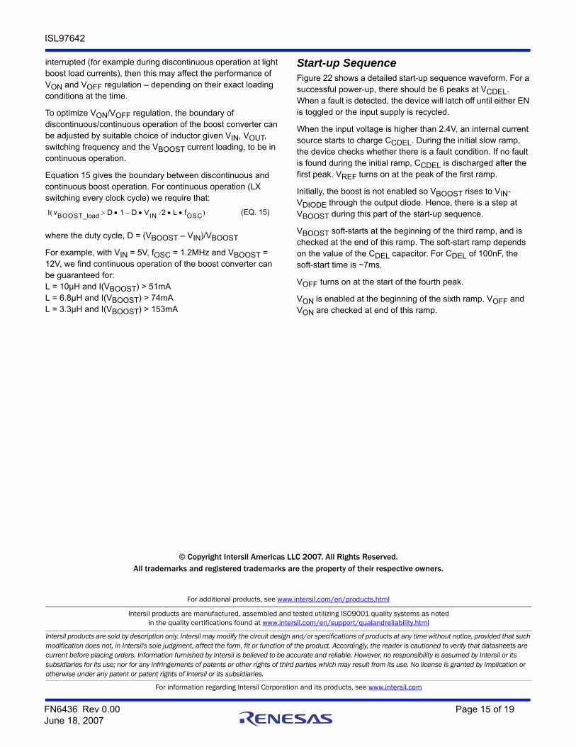
Start-up SequenceFigure 22 shows a detailed start-up sequence waveform. For a successful power-up, there should be 6 peaks at VCDEL. When a fault is detected, the device will latch off until either EN is toggled or the input supply is recycled.
When the input voltage is higher than 2.4V, an internal current source starts to charge CCDEL. During the initial slow ramp, the device checks whether there is a fault condition. If no fault is found during the initial ramp, CCDEL is discharged after the first peak. VREF turns on at the peak of the first ramp.
Initially, the boost is not enabled so VBOOST rises to VIN-VDIODE through the output diode. Hence, there is a step at VBOOST during this part of the start-up sequence.
VBOOST soft-starts at the beginning of the third ramp, and is checked at the end of this ramp. The soft-start ramp depends on the value of the CDEL capacitor. For CDEL of 100nF, the soft-start time is ~7ms.
VOFF turns on at the start of the fourth peak.
VON is enabled at the beginning of the sixth ramp. VOFF and VON are checked at end of this ramp.
I vBOOST_load D 1 D VIN 2 L fOSC– (EQ. 15)
FN6436 Rev 0.00 Page 15 of 19June 18, 2007
ISL97642
Component Selection for Start-up Sequencing and Fault Protection
The CREF capacitor is typically set at 220nF and is required to stabilize the VREF output. The range of CREF is from 22nF to 1µF and should not be more than five times the capacitor on CDEL to ensure correct start-up operation.
The CDEL capacitor is typically 100nF and has a usable range from 22nF minimum to several microfarads – only limited by the leakage in the capacitor reaching µA levels. CDEL should be at least 1/5 of the value of CREF (see Figure 22). Note that with
100nF on CDEL, the fault time-out will be typically 23ms and the use of a larger/smaller value will vary this time proportionally (e.g. 1µF will give a fault time-out period of typically 230ms).
Fault Sequencing
The ISL97642 has an advanced fault detection system, which protects the IC from both adjacent pin shorts during operation and shorts on the output supplies. A high quality layout/design of the PCB (in respect of grounding quality and decoupling) is necessary to avoid falsely triggering the fault detection scheme – especially during start-up. The user is directed to the layout
VCDEL
IN
VREF
VBOOST
VOFF
VON
VR
EF O
N
VB
OO
ST
SO
FT
-ST
AR
T
VO
FF O
N
VO
N S
OF
T-S
TA
RT
FA
UL
T D
ET
EC
TE
D
CH
IP D
ISA
BL
ED
NORMALOPERATION
FAULTPRESENT
START-UP SEQUENCETIMED BY CDEL
tON
tDEL1
tDEL2
tDEL3
VON SLICE CIRCUIT
FIGURE 22. START-UP SEQUENCE
NOTE: Not to scale
FN6436 Rev 0.00 Page 16 of 19June 18, 2007
ISL97642
guidelines and component selection sections to avoid problems during initial evaluation and prototype PCB generation.
VON-Slice Circuit
The VON-slice Circuit functions as a three way multiplexer, switching the voltage on COM between ground, DRN and SRC, under control of the start-up sequence and the CTL pin.
Once the start-up sequence has completed, CTL is enabled and acts as a multiplexer control such that if CTL is low, COM connects to DRN through a 5internal MOSFET, and if CTL is high, COM connects to SRC via a 30MOSFET.
The slew rate of start-up of the switch control circuit is mainly restricted by the load capacitance at COM pin, as in Equation 16:
Where Vg is the supply voltage applied to the switch control circuit, Ri is the resistance between COM and DRN or SRC including the internal MOSFET rDS(ON), the trace resistance and the resistor inserted; RL is the load resistance of the switch control circuit, and CL is the load capacitance of the switch control circuit.
In the “Typical Application Circuit” on page 18, R8, R9 and C8 give the bias to DRN based on Equation 17:
and R10 can be adjusted to adjust the slew rate.
Op AmpsThe ISL97642 has 3 amplifiers respectively. The op amps are typically used to drive the TFT-LCD backplane (VCOM) or the gamma-correction divider string. They feature rail-to-rail input and output capability. They are unity gain stable, and have low power consumption (typical 600A per amplifier). The ISL97642 has a -3dB bandwidth of 12MHz while maintaining a 10V/s slew rate.
Short Circuit Current Limit
The ISL97642 will limit the short circuit current to ±180mA if the output is directly shorted to the positive or the negative supply. If an output is shorted for a long time, the junction temperature will trigger the Over-Temperature Protection limit and, hence, the part will shut down.
Driving Capacitive Loads
ISL97642 can drive a wide range of capacitive loads. As load capacitance increases, however, the -3dB bandwidth of the device will decrease and the peaking will increase. The amplifiers drive 10pF loads in parallel with 10k with just 1.5dB of peaking, and 100pF with 6.4dB of peaking. If less peaking is desired in these applications, a small series resistor (usually between 5 and 50) can be placed in series with the output. However, this will obviously reduce the gain. Another
method of reducing peaking is to add a “snubber” circuit at the output. A snubber is a shunt load consisting of a resistor in series with a capacitor. Values of 150 and 10nF are typical. The advantage of a snubber is that it does not draw any DC load current and reduce the gain.
Over-Temperature ProtectionAn internal temperature sensor continuously monitors the die temperature. In the event that the die temperature exceeds the thermal trip point, the device will be latched off until either the input supply voltage or enable is cycled.
Layout RecommendationThe devices performance (including efficiency, output noise, transient response and control loop stability) is dramatically affected by the PCB layout. PCB layout is critical, especially at high switching frequency.
There are some general guidelines for layout:
1. Place the external power components (the input capacitors, output capacitors, boost inductor and output diodes, etc.) in close proximity to the device. Traces to these components should be kept as short and wide as possible to minimize parasitic inductance and resistance.
2. Place VREF and VDD bypass capacitors close to the pins.
3. Reduce the loop with large AC amplitudes and fast slew rate.
4. The feedback network should sense the output voltage directly from the point of load, and be as far away from LX node as possible.
5. The power ground (PGND) and signal ground (SGND) pins should be connected at only one point.
6. The exposed die plate, on the underneath of the package, should be soldered to an equivalent area of metal on the PCB. This contact area should have multiple via connections to the back of the PCB as well as connections to intermediate PCB layers (if available) to maximize thermal dissipation away from the IC.
7. To minimize the thermal resistance of the package when soldered to a multi-layer PCB, the amount of copper track and ground plane area connected to the exposed die plate should be maximized and spread out as far as possible from the IC. The bottom and top PCB areas especially should be maximized to allow thermal dissipation to the surrounding air.
8. A signal ground plane, separate from the power ground plane and connected to the power ground pins only at the exposed die plate, should be used for ground return connections for feedback resistor networks (R1, R11, R41) and the VREF capacitor, C22, the CDELAY capacitor C7 and the integrator capacitor C23.
9. Minimize feedback input track lengths to avoid switching noise pick-up.
A demo board is available to illustrate the proper layout implementation.
Vt--------
VgRi RL
CL------------------------------------= (EQ. 16)
VDRN
VON R9 AVDD R8+
R8 R9+-------------------------------------------------------------= (EQ. 17)
FN6436 Rev 0.00 Page 17 of 19June 18, 2007
ISL97642
Typical Application Circuit
-+
-+
-+
BOOST
POSREG
SWCTL
NEGREG
REF
VIN(2.6V TO 5.5V)
10µF
IN
COMP
DRVN
FBN
REF
CTL
DEL
100nF
CONTROLINPUT
AVDD
NEG3
OUT3
POS3
NEG2
OUT2
POS2VCOM SET2
VCOM2
VCOM FB2
VCOM SET3
VCOM3
VCOM FB3
VMAIN
AGND
OP2
OP3
POS1VCOM SET1
OP1
OUT1VCOM1
NEG1VCOM FB1
DRN
COM
R868k
C80.1µF
R91k
AVDD
SRC
FBP
DRVP 700
182k
9.76k
470nF
0.1µF
VCP
VON(24.5V)
GND
PGND
FB
10.2k
64.9k
10µFx2
AVDD(9V)
VCP
0.1µF
0.1µF
0.1µF0.1µF
L1
VCN
0.1µF
470nF
VNEG(-8V)
VCN700
82k
10k
LX
TO GATE DRIVER IC
180
2.2nF
0.1µF
10
470nF
D11
D12D21
C16.8µH
D1
C2
R2
R1
R12
R11
Q11Q21
R22
R21
R7 OPEN
C7 OPEN
FN6436 Rev 0.00 Page 18 of 19June 18, 2007
ISL97642
FN6436 Rev 0.00 Page 19 of 19June 18, 2007
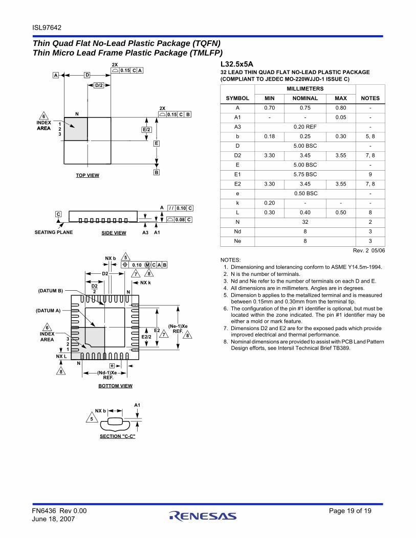
Thin Quad Flat No-Lead Plastic Package (TQFN)Thin Micro Lead Frame Plastic Package (TMLFP)
INDEX
D/2
D
E/2
E
A
B
C
0.10 BAM C
A
N
SEATING PLANE
N
6
32
23
e
1
1
0.08
SECTION "C-C"
NX bA1
2XC0.15
0.152X
B
REF.(Nd-1)Xe
(Ne-1)XeREF.
5
A1
A
C
C
A3
D2
D2
E2E2/2
SIDE VIEW
TOP VIEW
7
BOTTOM VIEW
7
5
2
NX k
NX b
8
NX L
8
8
AREA
0.10 C/ /
(DATUM B)
(DATUM A)
AREA
INDEX6
AREA
N
L32.5x5A32 LEAD THIN QUAD FLAT NO-LEAD PLASTIC PACKAGE(COMPLIANT TO JEDEC MO-220WJJD-1 ISSUE C)
SYMBOL
MILLIMETERS
NOTESMIN NOMINAL MAX
A 0.70 0.75 0.80 -
A1 - - 0.05 -
A3 0.20 REF -
b 0.18 0.25 0.30 5, 8
D 5.00 BSC -
D2 3.30 3.45 3.55 7, 8
E 5.00 BSC -
E1 5.75 BSC 9
E2 3.30 3.45 3.55 7, 8
e 0.50 BSC -
k 0.20 - - -
L 0.30 0.40 0.50 8
N 32 2
Nd 8 3
Ne 8 3
Rev. 2 05/06
NOTES:1. Dimensioning and tolerancing conform to ASME Y14.5m-1994.2. N is the number of terminals.3. Nd and Ne refer to the number of terminals on each D and E. 4. All dimensions are in millimeters. Angles are in degrees. 5. Dimension b applies to the metallized terminal and is measured
between 0.15mm and 0.30mm from the terminal tip.6. The configuration of the pin #1 identifier is optional, but must be
located within the zone indicated. The pin #1 identifier may beeither a mold or mark feature.
7. Dimensions D2 and E2 are for the exposed pads which provide improved electrical and thermal performance.
8. Nominal dimensions are provided to assist with PCB Land Pattern Design efforts, see Intersil Technical Brief TB389.


![Application Note - IST AG · HT: Higher temperature limit [= +150 °C] V+: Supply voltage [V] Sig[V]: Analog/ratiometric output signal [V] 2. TSic 506F/503F/516/501F The TSic series](https://img.pdfslide.us/doc/110x75/5ecabbcceb0260094e3d2567/application-note-ist-ag-ht-higher-temperature-limit-150-c-v-supply-voltage.jpg)