Embed Size (px)
Citation preview
1300 Henley Court Pullman, WA 99163
509.334.6306 www.digilentinc.com
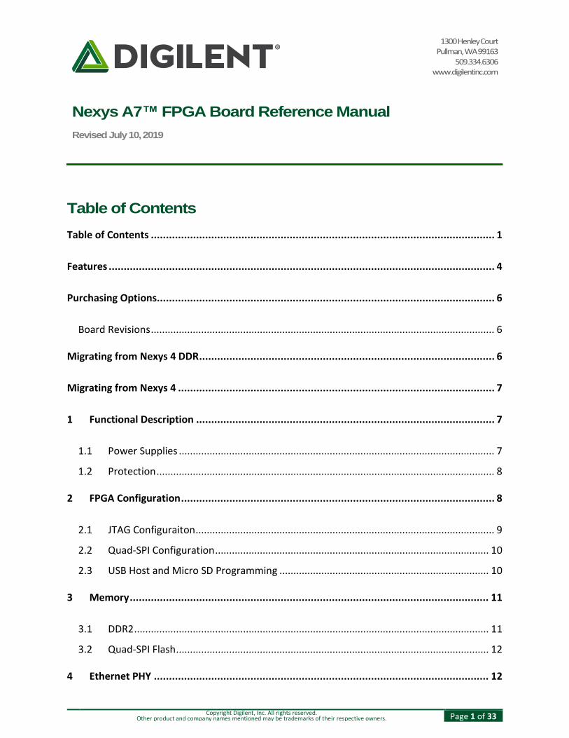
Nexys A7™ FPGA Board Reference Manual
Revised July 10, 2019
Copyright Digilent, Inc. All rights reserved. Other product and company names mentioned may be trademarks of their respective owners. Page 1 of 33
Table of Contents
Table of Contents .................................................................................................................. 1
Features ................................................................................................................................ 4
Purchasing Options ................................................................................................................ 6
Board Revisions ........................................................................................................................... 6
Migrating from Nexys 4 DDR .................................................................................................. 6
Migrating from Nexys 4 ......................................................................................................... 7
1 Functional Description ................................................................................................... 7
1.1 Power Supplies ................................................................................................................. 7
1.2 Protection ......................................................................................................................... 8
2 FPGA Configuration ........................................................................................................ 8
2.1 JTAG Configuraiton ........................................................................................................... 9
2.2 Quad-SPI Configuration .................................................................................................. 10
2.3 USB Host and Micro SD Programming ........................................................................... 10
3 Memory ....................................................................................................................... 11
3.1 DDR2 ............................................................................................................................... 11
3.2 Quad-SPI Flash ................................................................................................................ 12
4 Ethernet PHY ............................................................................................................... 12
Nexys A7™ FPGA Board Reference Manual
Copyright Digilent, Inc. All rights reserved. Other product and company names mentioned may be trademarks of their respective owners. Page 2 of 33
5 Oscillators/Clocks ........................................................................................................ 13
6 USB-UART Bridge (Serial Port) ...................................................................................... 14
7 USB HID Host ............................................................................................................... 14
7.1 HID Controller ................................................................................................................. 15
7.2 Keyboard ........................................................................................................................ 16
7.3 Mouse ............................................................................................................................. 17
8 VGA Port ...................................................................................................................... 18
8.1 VGA System Timing ........................................................................................................ 18
9 Basic I/O ...................................................................................................................... 22
9.1 Seven-Segment Display .................................................................................................. 23
9.2 Tri-Color LED ................................................................................................................... 24
10 Pmod Ports .................................................................................................................. 25
10.1 Dual Analog/Digital Pmod .......................................................................................... 25
11 MicroSD Slot ................................................................................................................ 26
12 Temperature Sensor..................................................................................................... 26
12.1 I2C Interface ................................................................................................................ 27
12.2 Open Drain Outputs .................................................................................................... 27
12.3 Quick Start Operation ................................................................................................. 27
13 Accelerometer ............................................................................................................. 27
13.1 SPI Interface ................................................................................................................ 28
13.2 Interrupts .................................................................................................................... 28
14 Microphone ................................................................................................................. 28
14.1 Pulse Density Modulation (PDM) ............................................................................... 29
14.2 Microphone Digital Interface Timing .......................................................................... 30
Nexys A7™ FPGA Board Reference Manual
Copyright Digilent, Inc. All rights reserved. Other product and company names mentioned may be trademarks of their respective owners. Page 3 of 33
15 Mono Audio Output ..................................................................................................... 30
15.2 Pulse-Width Modulation ............................................................................................ 31
Built-In Self-Test .................................................................................................................. 32
Nexys A7™ FPGA Board Reference Manual
Copyright Digilent, Inc. All rights reserved. Other product and company names mentioned may be trademarks of their respective owners. Page 4 of 33
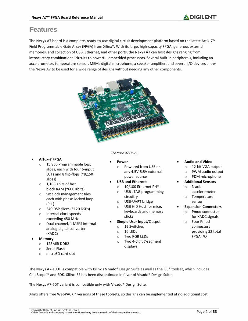
Features
The Nexys A7 board is a complete, ready-to-use digital circuit development platform based on the latest Artix-7™
Field Programmable Gate Array (FPGA) from Xilinx®. With its large, high-capacity FPGA, generous external
memories, and collection of USB, Ethernet, and other ports, the Nexys A7 can host designs ranging from
introductory combinational circuits to powerful embedded processors. Several built-in peripherals, including an
accelerometer, temperature sensor, MEMs digital microphone, a speaker amplifier, and several I/O devices allow
the Nexys A7 to be used for a wide range of designs without needing any other components.
The Nexys A7 FPGA.
The Nexys A7-100T is compatible with Xilinx’s Vivado® Design Suite as well as the ISE® toolset, which includes
ChipScope™ and EDK. Xilinx ISE has been discontinued in favor of Vivado® Design Suite.
The Nexys A7-50T variant is compatible only with Vivado® Design Suite.
Xilinx offers free WebPACK™ versions of these toolsets, so designs can be implemented at no additional cost.
• Artux-7 FPGA o 15,850 Programmable logic
slices, each with four 6-input LUTs and 8 flip-flops (*8,150 slices)
o 1,188 Kbits of fast block RAM (*600 Kbits)
o Six clock management tiles, each with phase-locked loop (PLL)
o 240 DSP slices (*120 DSPs) o Internal clock speeds
exceeding 450 MHz o Dual-channel, 1 MSPS internal
analog-digital converter (XADC)
• Memory o 128MiB DDR2 o Serial Flash o microSD card slot
• Power o Powered from USB or
any 4.5V-5.5V external power source
• USB and Ethernet o 10/100 Ethernet PHY o USB-JTAG programming
circuitry o USB-UART bridge o USB HID Host for mice,
keyboards and memory sticks
• Simple User Input/Output o 16 Switches o 16 LEDs o Two RGB LEDs o Two 4-digit 7-segment
displays
• Audio and Video o 12-bit VGA output o PWM audio output o PDM microphone
• Additional Sensors o 3-axis
accelerometer o Temperature
sensor
• Expansion Connectors o Pmod connector
for XADC signals o Four Pmod
connectors providing 32 total FPGA I/O
Nexys A7™ FPGA Board Reference Manual
Copyright Digilent, Inc. All rights reserved. Other product and company names mentioned may be trademarks of their respective owners. Page 5 of 33
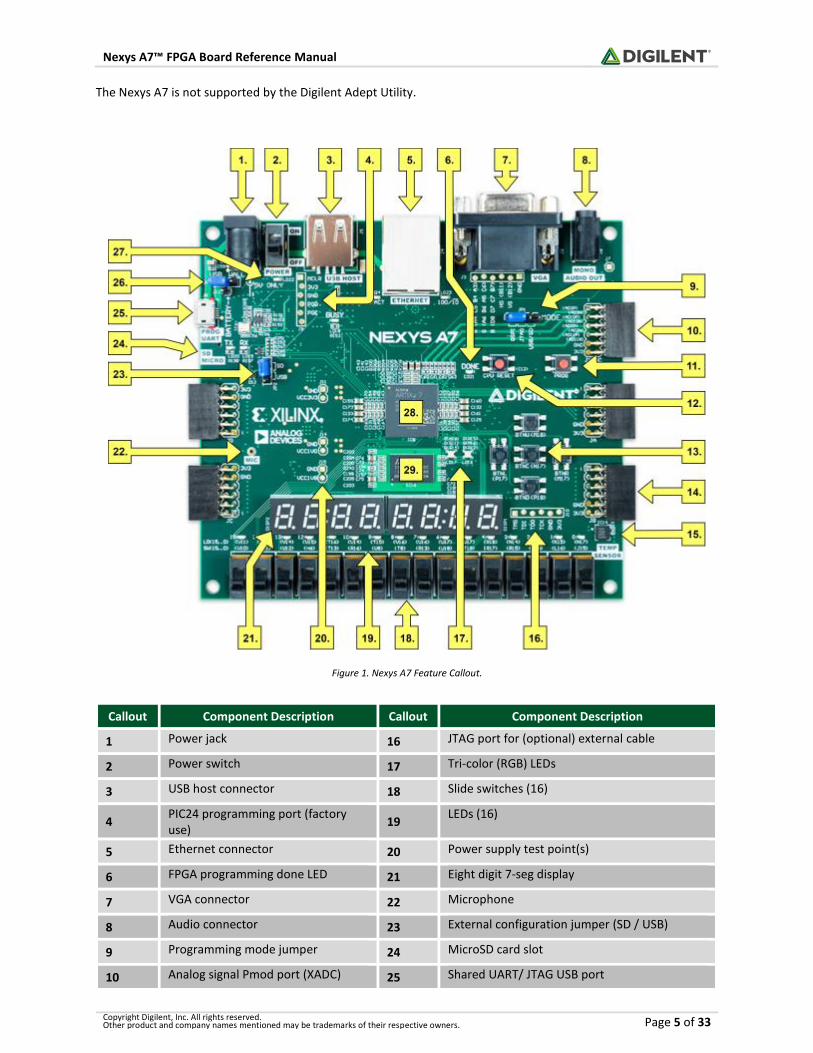
The Nexys A7 is not supported by the Digilent Adept Utility.
Figure 1. Nexys A7 Feature Callout.
Callout Component Description Callout Component Description
1 Power jack 16 JTAG port for (optional) external cable
2 Power switch 17 Tri-color (RGB) LEDs
3 USB host connector 18 Slide switches (16)
4 PIC24 programming port (factory use)
19 LEDs (16)
5 Ethernet connector 20 Power supply test point(s)
6 FPGA programming done LED 21 Eight digit 7-seg display
7 VGA connector 22 Microphone
8 Audio connector 23 External configuration jumper (SD / USB)
9 Programming mode jumper 24 MicroSD card slot
10 Analog signal Pmod port (XADC) 25 Shared UART/ JTAG USB port
Nexys A7™ FPGA Board Reference Manual
Copyright Digilent, Inc. All rights reserved. Other product and company names mentioned may be trademarks of their respective owners. Page 6 of 33
Purchasing Options
The Nexys A7 can be purchased with either a XC7A100T or XC7A50T FPGA loaded. These two Nexys A7 product
variants are referred to as the Nexys A7-100T and Nexys A7-50T, respectively. When Digilent documentation
describes functionality that is common to both of these variants, they are referred to collectively as the “Nexys
A7”. When describing something that is only common to a specific variant, the variant will be explicitly called out
by its name.
The only difference between the Nexys A7-100T and Nexys A7-50T is the size of the Artix-7 part. The Artix-7 FPGAs
both have the same capabilities, but the XC7100T has about a 2 times larger internal FPGA than the XC750T. The
differences between the two variants are summarized below:
Board Revisions
The Nexys A7 is a rebrand of the Nexys 4 DDR board, which is an incremental update to the Nexys 4 board.
Migrating from Nexys 4 DDR
The only difference between the Nexys A7 and Nexys 4 DDR is the addition of the Nexys A7-50T variant of the
Nexys A7, which has a smaller gate array. The Nexys A7-100T variant is functionally identical to the Nexys 4 DDR.
Users of the Nexys A7 may find resources produced for the Nexys 4 DDR helpful, which can be found at the Nexys
4 DDR's Resource Center.
11 FPGA configuration reset button 26 Power select jumper and battery header
12 CPU reset button (for soft cores) 27 Power-good LED
13 Five pushbuttons 28 Xilinx Artix-7 FPGA
14 Pmod port(s) 29 DDR2 memory
15 Temperature sensor
Product Variant Nexys A7-100T Nexys A7-50T
FPGA Part Number XC7A100T-1CSG324C XC7A50T-1CSG324I
Look-up Tables (LUTs) 63,400 32,600
Flip-Flops 126,800 65,200
Block RAM 1,188 Kb 600 Kb
DSP Slices 240 120
Clock Management Tiles 6 5
Nexys A7™ FPGA Board Reference Manual
Copyright Digilent, Inc. All rights reserved. Other product and company names mentioned may be trademarks of their respective owners. Page 7 of 33
Migrating from Nexys 4
The major improvement from the Nexys 4 to the Nexys 4 DDR is the replacement of the 16 MiB Cellular RAM with
a 128 MiB DDR2 SDRAM memory. Furthermore, to accommodate the new memory, the pin-out of the FPGA banks
changed as well.
The audio output (AUD_PWM) needs to be driven open-drain as opposed to push-pull on the Nexys 4.
1 Functional Description
1.1 Power Supplies
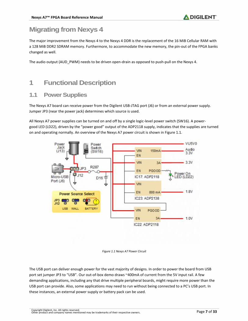
The Nexys A7 board can receive power from the Digilent USB-JTAG port (J6) or from an external power supply.
Jumper JP3 (near the power jack) determines which source is used.
All Nexys A7 power supplies can be turned on and off by a single logic-level power switch (SW16). A power-
good LED (LD22), driven by the “power good” output of the ADP2118 supply, indicates that the supplies are turned
on and operating normally. An overview of the Nexys A7 power circuit is shown in Figure 1.1.
Figure 1.1 Nexys A7 Power Circuit
The USB port can deliver enough power for the vast majority of designs. In order to power the board from USB
port set jumper JP3 to “USB”. Our out-of-box demo draws ~400mA of current from the 5V input rail. A few
demanding applications, including any that drive multiple peripheral boards, might require more power than the
USB port can provide. Also, some applications may need to run without being connected to a PC’s USB port. In
these instances, an external power supply or battery pack can be used.
Nexys A7™ FPGA Board Reference Manual
Copyright Digilent, Inc. All rights reserved. Other product and company names mentioned may be trademarks of their respective owners. Page 8 of 33
An external power supply can be used by plugging into to the power jack (J13) and setting jumper JP3 to “WALL”.
The supply must use a coax, center-positive 2.1mm internal-diameter plug, and deliver 4.5VDC to 5.5VDC and at
least 1A of current (i.e., at least 5W of power). Many suitable supplies can be purchased from Digilent, through
Digi-Key, or other catalog vendors.
An external battery pack can be used by connecting the battery’s positive terminal to the center pin of JP3 and the
negative terminal to the pin labeled J12, directly below JP3. Since the main regulator on the Nexys A7 cannot
accommodate input voltages over 5.5VDC, an external battery pack must be limited to 5.5VDC. The minimum
voltage of the battery pack depends on the application: if the USB Host function (J5) is used, at least 4.6V needs to
be provided. In other cases, the minimum voltage is 3.6V.
Voltage regulator circuits from Analog Devices create the required 3.3V, 1.8V, and 1.0V supplies from the main
power input. Table 1.1 provides additional information. Typical currents depend strongly on FPGA configuration
and the values provided are typical of medium size/speed designs.
Supply Circuits Device Current (Max/Typical)
3.3V FPGA I/O, USB ports, Clocks, RAM I/O, Ethernet, SD slot, Sensors, Flash
IC17: ADP2118 3A/0.1 to 1.5A
1.0V FPGA Core IC22: ADP2118 3A/ 0.2 to 1.3A
1.8V DDR2, FPGA Auxiliary and RAM IC23: ADP2118 0.8A/ 0.5A
Table 1.1 Nexys A7 power supplies.
1.2 Protection
The Nexys A7 features overcurrent and overvoltage protection on the input power rail. A 3.5A fuse (R287) and a 5V
Zener diode (D16) provide a non-resettable protection for other on-board integrated circuits, as displayed in Figure
2. Applying power outside of the specs outlined in this document is not covered by warranty. If this happens,
either or both might get permanently damaged. The damaged parts are not user replaceable.
2 FPGA Configuration
After power-on, the Artix-7 FPGA must be configured (or programmed) before it can perform any functions. You
can configure the FPGA in one of four ways:
1. A PC can use the Digilent USB-JTAG circuitry (portJ6, labeled “PROG”) to program the FPGA any time the
power is on.
2. A file stored in the nonvolatile serial (SPI) flash device can be transferred to the FPGA using the SPI port.
3. A programming file can be transferred to the FPGA from a micro SD card.
4. A programming file can be transferred from a USB memory stick attached to the USB HID port.
Nexys A7™ FPGA Board Reference Manual
Copyright Digilent, Inc. All rights reserved. Other product and company names mentioned may be trademarks of their respective owners. Page 9 of 33
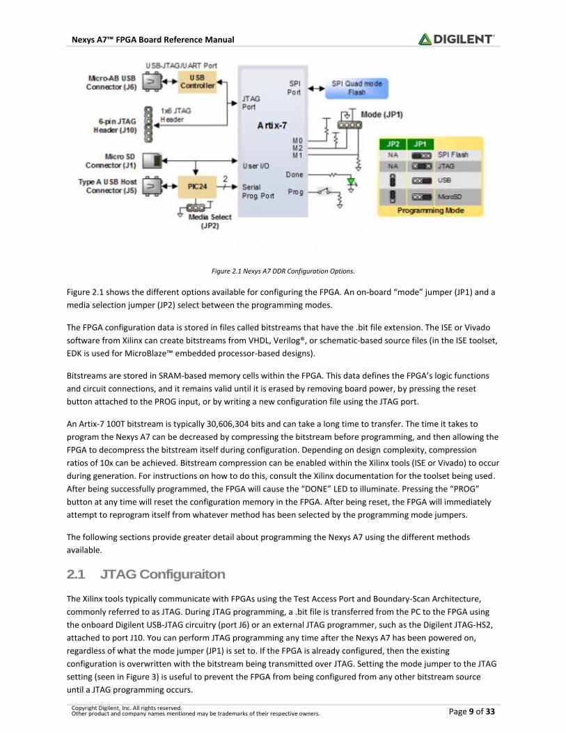
Figure 2.1 Nexys A7 DDR Configuration Options.
Figure 2.1 shows the different options available for configuring the FPGA. An on-board “mode” jumper (JP1) and a
media selection jumper (JP2) select between the programming modes.
The FPGA configuration data is stored in files called bitstreams that have the .bit file extension. The ISE or Vivado
software from Xilinx can create bitstreams from VHDL, Verilog®, or schematic-based source files (in the ISE toolset,
EDK is used for MicroBlaze™ embedded processor-based designs).
Bitstreams are stored in SRAM-based memory cells within the FPGA. This data defines the FPGA’s logic functions
and circuit connections, and it remains valid until it is erased by removing board power, by pressing the reset
button attached to the PROG input, or by writing a new configuration file using the JTAG port.
An Artix-7 100T bitstream is typically 30,606,304 bits and can take a long time to transfer. The time it takes to
program the Nexys A7 can be decreased by compressing the bitstream before programming, and then allowing the
FPGA to decompress the bitstream itself during configuration. Depending on design complexity, compression
ratios of 10x can be achieved. Bitstream compression can be enabled within the Xilinx tools (ISE or Vivado) to occur
during generation. For instructions on how to do this, consult the Xilinx documentation for the toolset being used.
After being successfully programmed, the FPGA will cause the “DONE” LED to illuminate. Pressing the “PROG”
button at any time will reset the configuration memory in the FPGA. After being reset, the FPGA will immediately
attempt to reprogram itself from whatever method has been selected by the programming mode jumpers.
The following sections provide greater detail about programming the Nexys A7 using the different methods
available.
2.1 JTAG Configuraiton
The Xilinx tools typically communicate with FPGAs using the Test Access Port and Boundary-Scan Architecture,
commonly referred to as JTAG. During JTAG programming, a .bit file is transferred from the PC to the FPGA using
the onboard Digilent USB-JTAG circuitry (port J6) or an external JTAG programmer, such as the Digilent JTAG-HS2,
attached to port J10. You can perform JTAG programming any time after the Nexys A7 has been powered on,
regardless of what the mode jumper (JP1) is set to. If the FPGA is already configured, then the existing
configuration is overwritten with the bitstream being transmitted over JTAG. Setting the mode jumper to the JTAG
setting (seen in Figure 3) is useful to prevent the FPGA from being configured from any other bitstream source
until a JTAG programming occurs.
Nexys A7™ FPGA Board Reference Manual
Copyright Digilent, Inc. All rights reserved. Other product and company names mentioned may be trademarks of their respective owners. Page 10 of 33
Programming the Nexys A7 with an uncompressed bitstream using the on-board USB-JTAG circuitry usually takes
around five seconds. JTAG programming can be done using the hardware server in Vivado or the iMPACT tool
included with ISE and the Lab Tools version of Vivado. The demonstration project available
at http://www.digilentinc.com/ gives an in-depth tutorial on how to program your board.
2.2 Quad-SPI Configuration
Since the FPGA on the Nexys A7 is volatile, it relies on the Quad-SPI flash memory to store the configuration
between power cycles. This configuration mode is called Master SPI. The blank FPGA takes the role of master and
reads the configuration file out of the flash device upon power-up. To that effect, a configuration file needs to be
downloaded first to the flash. When programming a nonvolatile flash device, a bitstream file is transferred to the
flash in a two-step process. First, the FPGA is programmed with a circuit that can program flash devices, and then
data is transferred to the flash device via the FPGA circuit (this complexity is hidden from the user by the Xilinx
tools). This is called indirect programming. After the flash device has been programmed, it can automatically
configure the FPGA at a subsequent power-on or reset event as determined by the mode jumper setting (see
Figure 3). Programming files stored in the flash device will remain until they are overwritten, regardless of power-
cycle events.
Programming the flash can take as long as four to five minutes, which is mostly due to the lengthy erase process
inherent to the memory technology. Once written however, FPGA configuration can be very fast—less than a
second. Bitstream compression, SPI bus width, and configuration rate are factors controlled by the Xilinx tools that
can affect configuration speed. The Nexys A7 supports x1, x2, and x4 bus widths and data rates of up to 50 MHz for
Quad-SPI programming.
Quad-SPI programming can be done using the iMPACT tool included with ISE or the Lab Tools version of Vivado.
2.3 USB Host and Micro SD Programming
You can program the FPGA from a pen drive attached to the USB Host port (J5) or a microSD card inserted into J1
by doing the following:
1. Format the storage device (Pen drive or microSD card) with a FAT32 file system.
2. Place a single .bit configuration file in the root directory of the storage device.
3. Attach the storage device to the Nexys A7.
4. Set the JP1 Programming Mode jumper on the Nexys A7 to “USB/SD”.
5. Select the desired storage device using JP2.
6. Push the PROG button or power-cycle the Nexys A7.
The FPGA will automatically configure with the .bit file on the selected storage device. Any .bit files that are not
built for the proper Artix-7 device will be rejected by the FPGA.
The Auxiliary Function Status, or “BUSY” LED, gives visual feedback on the state of the configuration process when
the FPGA is not yet programmed:
• When steadily lit, the auxiliary microcontroller is either booting up or currently reading the configuration
medium (microSD or pen drive) and downloading a bitstream to the FPGA.
• A slow pulse means the microcontroller is waiting for a configuration medium to be plugged in.
• In case of an error during configuration, the LED will blink rapidly.
When the FPGA has been successfully configured, the behavior of the LED is application-specific. For example, if a
USB keyboard is plugged in, a rapid blink will signal the receipt of an HID input report from the keyboard.
Nexys A7™ FPGA Board Reference Manual
Copyright Digilent, Inc. All rights reserved. Other product and company names mentioned may be trademarks of their respective owners. Page 11 of 33
3 Memory
The Nexys A7 board contains two external memories: a 1Gib (128MiB) DDR2 SDRAM and a 128Mib (16MiB) non-
volatile serial Flash device. The DDR2 modules are integrated on-board and connect to the FPGA using the industry
standard interface. The serial Flash is on a dedicated quad-mode (x4) SPI bus. The connections and pin assignments
between the FPGA and external memories are shown below.
3.1 DDR2
The Nexys A7 includes one Micron MT47H64M16HR-25:H DDR2 memory component, creating a single rank, 16-bit
wide interface. It is routed to a 1.8V-powered HR (High Range) FPGA bank with 50 ohm controlled single-ended
trace impedance. 50-ohm internal terminations in the FPGA are used to match the trace characteristics. Similarly,
on the memory side, on-die terminations (ODT) are used for impedance matching.
For proper operation of the memory, a memory controller and physical layer (PHY) interface needs to be included
in the FPGA design. There are two recommended ways to do that, which are outlined below and differ in
complexity and design flexibility.
The straightforward way is to use the Digilent-provided DDR-to-SRAM adapter module which instantiates the
memory controller and uses an asynchronous SRAM bus for interfacing with user logic. This module provides
backward compatibility with projects written for older Nexys-line boards featuring a CellularRAM instead of DDR2.
It trades memory bandwidth for simplicity.
More advanced users or those who wish to learn more about DDR SDRAM technology may want to use the Xilinx
7-series memory interface solutions core generated by the MIG (Memory Interface Generator) Wizard. Depending
on the tool used (ISE, EDK or Vivado), the MIG Wizard can generate a native FIFO-style or an AXI4 interface to
connect to user logic. This workflow allows the customization of several DDR parameters optimized for the
particular application. Table 3.1 below lists the MIG Wizard settings optimized for the Nexys A7.
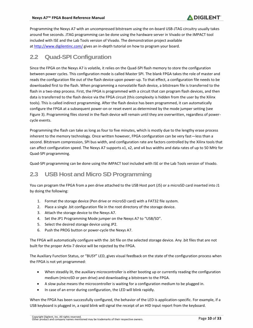
Setting Value
Memory type DDR2 SDRAM
Max. clock period 3000ps (667Mbps data rate)
Recommended clock period (for easy clock generation) 3077ps (650Mbps data rate)
Memory part MT47H64M16HR-25E
Data width 16
Data mask Enabled
Chip Select pin Enabled
Rtt (nominal) – On-die termination 50ohms
Internal Vref Enabled
Table 3.1.1 DDR2 settings for the Nexys A7.
Although the FPGA, memory IC, and the board itself are capable of the maximum data rate of 667Mbps, the
limitations in the clock generation primitives restrict the clock frequencies that can be generated from the
100 MHz system clock. Thus, for simplicity, the next highest data rate of 650Mbps is recommended.
The MIG Wizard will require the fixed pin-out of the memory signals to be entered and validated before generating
the IP core. For your convenience, an importable UCF file is provided on the Digilent website to speed up the
process.
Nexys A7™ FPGA Board Reference Manual
Copyright Digilent, Inc. All rights reserved. Other product and company names mentioned may be trademarks of their respective owners. Page 12 of 33
For more details on the Xilinx memory interface solutions, refer to the 7 Series FPGAs Memory Interface Solutions
User Guide (ug586)i.
3.2 Quad-SPI Flash
FPGA configuration files can be written to the Quad-SPI Flash (Spansion part number S25FL128S), and mode
settings are available to cause the FPGA to automatically read a configuration from this device at power on. An
Artix-7 100T configuration file requires just less than four MiB (mebibyte) of memory, leaving about 77% of the
flash device available for user data. Or, if the FPGA is getting configured from another source, the whole memory
can be used for custom data.
The contents of the memory can be manipulated by issuing certain commands on the SPI bus. The implementation
of this protocol is outside the scope of this document. All signals in the SPI bus except SCK are general-purpose
user I/O pins after FPGA configuration. SCK is an exception because it remains a dedicated pin even after
configuration. Access to this pin is provided through a special FPGA primitive called STARTUPE2.
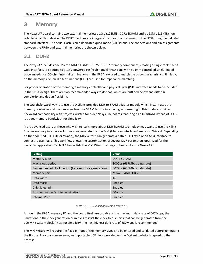
NOTE: Refer to the manufacturer’s data sheetsii and Xilinx user guidesiii for more information.
Figure 3.2.1 Nexys A7 DDR SPI Flash Pin-out
4 Ethernet PHY
The Nexys A7 board includes an SMSC 10/100 Ethernet PHY (SMSC part number LAN8720A) paired with an RJ-45
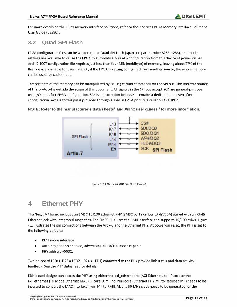
Ethernet jack with integrated magnetics. The SMSC PHY uses the RMII interface and supports 10/100 Mb/s. Figure
4.1 illustrates the pin connections between the Artix-7 and the Ethernet PHY. At power-on reset, the PHY is set to
the following defaults:
• RMII mode interface
• Auto-negotiation enabled, advertising all 10/100 mode capable
• PHY address=00001
Two on-board LEDs (LD23 = LED2, LD24 = LED1) connected to the PHY provide link status and data activity
feedback. See the PHY datasheet for details.
EDK-based designs can access the PHY using either the axi_ethernetlite (AXI EthernetLite) IP core or the
axi_ethernet (Tri Mode Ethernet MAC) IP core. A mii_to_rmii core (Ethernet PHY MII to Reduced MII) needs to be
inserted to convert the MAC interface from MII to RMII. Also, a 50 MHz clock needs to be generated for the
Nexys A7™ FPGA Board Reference Manual
Copyright Digilent, Inc. All rights reserved. Other product and company names mentioned may be trademarks of their respective owners. Page 13 of 33
mii_to_rmii core and the CLKIN pin of the external PHY. To account for skew introduced by the mii_to_rmii core,
generate each clock individually, with the external PHY clock having a 45 degree phase shift relative to the
mii_to_rmii Ref_Clk. An EDK demonstration project that properly uses the Ethernet PHY can be found on the Nexys
A7 product page at http://www.digilentinc.com/.
ISE designs can use the IP Core Generator wizard to create an Ethernet MAC controller IP core.
NOTE: Refer to the LAN8720A data sheet for further informationiv.
Figure 4.1 Pin Connections between the Artix-7 and the Ethernet PHY
5 Oscillators/Clocks
The Nexys A7 board includes a single 100 MHz crystal oscillator connected to pin E3 (E3 is a MRCC input on bank
35). The input clock can drive MMCMs or PLLs to generate clocks of various frequencies and with known phase
relationships that may be needed throughout a design. Some rules restrict which MMCMs and PLLs may be driven
by the 100 MHz input clock. For a full description of these rules and of the capabilities of the Artix-7 clocking
resources, refer to the “7 Series FPGAs Clocking Resources User Guide” available from Xilinx.
Xilinx offers the Clocking Wizard IP core to help users generate the different clocks required for a specific design.
This wizard will properly instantiate the needed MMCMs and PLLs based on the desired frequencies and phase
relationships specified by the user. The wizard will then output an easy-to-use wrapper component around these
clocking resources that can be inserted into the user’s design. The clocking wizard can be accessed from within the
Project Navigator or Core Generator tools.
Nexys A7™ FPGA Board Reference Manual
Copyright Digilent, Inc. All rights reserved. Other product and company names mentioned may be trademarks of their respective owners. Page 14 of 33
6 USB-UART Bridge (Serial Port)
The Nexys A7 includes an FTDI FT2232HQ USB-UART bridge (attached to connector J6) that allows you use PC
applications to communicate with the board using standard Windows COM port commands. Free USB-COM port
drivers, available from http://www.ftdichip.com/ under the “Virtual Com Port” or VCP heading, convert USB
packets to UART/serial port data. Serial port data is exchanged with the FPGA using a two-wire serial port
(TXD/RXD) and optional hardware flow control (RTS/CTS). After the drivers are installed, I/O commands can be
used from the PC directed to the COM port to produce serial data traffic on the C4 and D4 FPGA pins.
Two on-board status LEDs provide visual feedback on traffic flowing through the port: the transmit LED (LD20) and
the receive LED (LD19). Signal names that imply direction are from the point-of-view of the DTE (Data Terminal
Equipment), in this case the PC.
The FT2232HQ is also used as the controller for the Digilent USB-JTAG circuitry, but the USB-UART and USB-JTAG
functions behave entirely independent of one another. Programmers interested in using the UART functionality of
the FT2232 within their design do not need to worry about the JTAG circuitry interfering with the UART data
transfers, and vice-versa. The combination of these two features into a single device allows the Nexys A7 to be
programmed, communicated with via UART, and powered from a computer attached with a single Micro USB
cable.
The connections between the FT2232HQ and the Artix-7 are shown in Figure 6.1.
Figure 6.1 Nexys A7 FT2322HQ Connections
7 USB HID Host
The Auxiliary Function microcontroller (Microchip PIC24FJ128) provides the Nexys A7 with USB Embedded HID
host capability. After power-up, the microcontroller is in configuration mode, either downloading a bitstream to
the FPGA, or waiting to be programmed from other sources. Once the FPGA is programmed, the microcontroller
switches to application mode, which is USB HID Host in this case. Firmware in the microcontroller can drive a
mouse or a keyboard attached to the type A USB connector at J5 labeled “USB Host”. Hub support is not currently
available, so only a single mouse or a single keyboard can be used. Only keyboards and mice supporting the Boot
HID interface are supported. The PIC24 drives several signals into the FPGA – two are used to implement a
standard PS/2 interface for communication with a mouse or keyboard, and the others are connected to the FPGA’s
two-wire serial programming port, so the FPGA can be programmed from a file stored on a USB pen drive or
microSD card.
Nexys A7™ FPGA Board Reference Manual
Copyright Digilent, Inc. All rights reserved. Other product and company names mentioned may be trademarks of their respective owners. Page 15 of 33
Figure 7.1 Nexys A7 PIC24 Connections
7.1 HID Controller
The Auxiliary Function microcontroller hides the USB HID protocol from the FPGA and emulates an old-style PS/2
bus. The microcontroller behaves just like a PS/2 keyboard or mouse would. This means new designs can re-use
existing PS/2 IP cores. Mice and keyboards that use the PS/2 protocol use a two-wire serial bus (clock and data) to
communicate with a host. On the Nexys A7, the microcontroller emulates a PS/2 device while the FPGA plays the
role of the host. Both the mouse and the keyboard use 11-bit words that include a start bit, data byte (LSB first),
odd parity, and stop bit, but the data packets are organized differently, and the keyboard interface allows bi-
directional data transfers (so the host device can illuminate state LEDs on the keyboard). Bus timings are shown in
Figure 7.1.1.
Figure 7.1.1 PS/2 Device-to-Host Timing Diagram
The clock and data signals are only driven when data transfers occur; otherwise, they are held in the idle state at
high-impedance (open-drain drivers). This requires that when the PS/2 signals are used in a design, internal pull-
ups must be enabled in the FPGA on the data and clock pins. The clock signal is normally driven by the device, but
may be held low by the host in special cases. The timings define signal requirements for mouse-to-host
communications and bi-directional keyboard communications. A PS/2 interface circuit can be implemented in the
FPGA to create a keyboard or mouse interface.
When a keyboard or mouse is connected to the Nexys A7, a “self-test passed” command (0xAA) is sent to the host.
After this, commands may be issued to the device. Since both the keyboard and the mouse use the same PS/2
port, one can tell the type of device connected using the device ID. This ID can be read by issuing a Read ID
Nexys A7™ FPGA Board Reference Manual
Copyright Digilent, Inc. All rights reserved. Other product and company names mentioned may be trademarks of their respective owners. Page 16 of 33
command (0xF2). Also, a mouse sends its ID (0x00) right after the “self-test passed” command, which distinguishes
it from a keyboard.
7.2 Keyboard
PS/2-style keyboards use scan codes to communicate key press data. Each key is assigned a code that is sent
whenever the key is pressed. If the key is held down, the scan code will be sent repeatedly about once every
100ms. When a key is released, an F0 key-up code is sent, followed by the scan code of the released key. If a key
can be shifted to produce a new character (like a capital letter), then a shift character is sent in addition to the scan
code and the host must determine which ASCII character to use. Some keys, called extended keys, send an E0
ahead of the scan code (and they may send more than one scan code). When an extended key is released, an E0 F0
key-up code is sent, followed by the scan code. Scan codes for most keys are shown in Figure 7.2.1.
Figure 7.2.1 Keyboard Scan Codes
A host device can also send data to the keyboard. Table 7.2.1 shows a list of some common commands a host
might send.
The keyboard can send data to the host only when both the data and clock lines are high (or idle). Because the
host is the bus master, the keyboard must check to see whether the host is sending data before driving the bus. To
facilitate this, the clock line is used as a “clear to send” signal. If the host drives the clock line low, the keyboard
must not send any data until the clock is released. The keyboard sends data to the host in 11-bit words that
contain a ‘0’ start bit, followed by 8-bits of scan code (LSB first), followed by an odd parity bit, and terminated with
a ‘1’ stop bit. The keyboard generates 11 clock transitions (at 20 to 30 KHz) when the data is sent, and data is valid
on the falling edge of the clock.
Command Action
ED Set Num Lock, Caps Lock, and Scroll Lock LEDs. Keyboard returns FA after receiving ED, then host sends a byte to set LED status: bit 0 sets Scroll Lock, bit 1 sets Num Lock, and bit 2 sets Caps lock. Bits 3 to 7 are ignored.
EE Echo (test). Keyboard returns EE after receiving EE
F3 Set scan code repeat rate. Keyboard returns F3 on receiving FA, then host sends second byte to set the repeat rate.
FE Resend. FE directs keyboard to re-send most recent scan code. Table 7.2.1. Keyboard commands.
Nexys A7™ FPGA Board Reference Manual
Copyright Digilent, Inc. All rights reserved. Other product and company names mentioned may be trademarks of their respective owners. Page 17 of 33
7.3 Mouse
Once entered in stream mode and data reporting is enabled, the mouse outputs a clock and data signal when it is
moved; otherwise, these signals remain at logic ‘1.’ Each time the mouse is moved, three 11-bit words are sent
from the mouse to the host device, as shown in Figure 7.3.1. Each of the 11-bit words contains a ‘0’ start bit,
followed by 8 bits of data (LSB first), followed by an odd parity bit, and terminated with a ‘1’ stop bit. Thus, each
data transmission contains 33 bits, where bits 0, 11, and 22 are ‘0’ start bits, and bits 11, 21, and 33 are ‘1’ stop
bits. The three 8-bit data fields contain movement data, as shown in Figure 7.3.1. Data is valid at the falling edge of
the clock, and the clock period is 20 to 30 KHz.
The mouse assumes a relative coordinate system wherein moving the mouse to the right generates a positive
number in the X field and moving to the left generates a negative number. Likewise, moving the mouse up
generates a positive number in the Y field, and moving down represents a negative number (the XS and YS bits in
the status byte are the sign bits – a ‘1’ indicates a negative number). The magnitude of the X and Y numbers
represent the rate of mouse movement; the larger the number, the faster the mouse is moving (the XV and YV bits
in the status byte are movement overflow indicators. A ‘1’ means overflow has occurred). If the mouse moves
continuously, the 33-bit transmissions are repeated every 50ms or so. The L and R fields in the status byte indicate
Left and Right button presses (a ‘1’ indicates the button is being pressed).
Figure 7.3.1 Mouse Data Format
The microcontroller also supports Microsoft® IntelliMouse®-type extensions for reporting back a third axis
representing the mouse wheel, as shown in Table 7.3.1.
Command Action
EA Set stream mode. The mouse responds with "acknowledge" (0xFA) then resets its movement counters and enters stream mode.
F4 Enable data reporting. The mouse responds with "acknowledge" (0xFA) then enables data reporting and resets its movement counters. This command only affects behavior in stream mode. Once issued, mouse movement will automatically generate a data packet.
F5 Disable data reporting. The mouse responds with "acknowledge" (0xFA) then disables data reporting and resets its movement counters.
F3 Set mouse sample rate. The mouse responds with "acknowledge" (0xFA) then reads one more byte from the host. This byte is then saved as the new sample rate, and a new “acknowledge” packet is issued.
FE Resend. FE directs mouse to re-send last packet.
Table 7.3.2. Microsoft IntelliMouse-Type extensions, commands, and actions.
Nexys A7™ FPGA Board Reference Manual
Copyright Digilent, Inc. All rights reserved. Other product and company names mentioned may be trademarks of their respective owners. Page 18 of 33
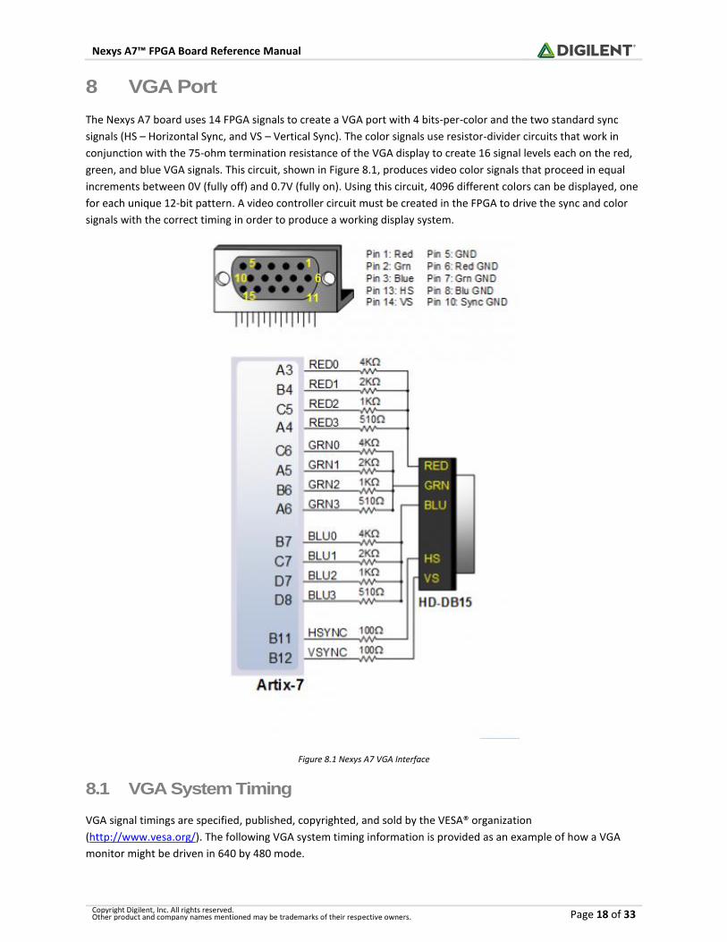
8 VGA Port
The Nexys A7 board uses 14 FPGA signals to create a VGA port with 4 bits-per-color and the two standard sync
signals (HS – Horizontal Sync, and VS – Vertical Sync). The color signals use resistor-divider circuits that work in
conjunction with the 75-ohm termination resistance of the VGA display to create 16 signal levels each on the red,
green, and blue VGA signals. This circuit, shown in Figure 8.1, produces video color signals that proceed in equal
increments between 0V (fully off) and 0.7V (fully on). Using this circuit, 4096 different colors can be displayed, one
for each unique 12-bit pattern. A video controller circuit must be created in the FPGA to drive the sync and color
signals with the correct timing in order to produce a working display system.
Figure 8.1 Nexys A7 VGA Interface
8.1 VGA System Timing
VGA signal timings are specified, published, copyrighted, and sold by the VESA® organization
(http://www.vesa.org/). The following VGA system timing information is provided as an example of how a VGA
monitor might be driven in 640 by 480 mode.
Nexys A7™ FPGA Board Reference Manual
Copyright Digilent, Inc. All rights reserved. Other product and company names mentioned may be trademarks of their respective owners. Page 19 of 33
NOTE: For more precise information, or for information on other VGA frequencies, refer to documentation
available at the VESA website.
CRT-based VGA displays use amplitude-modulated moving electron beams (or cathode rays) to display information
on a phosphor-coated screen. LCD displays use an array of switches that can impose a voltage across a small
amount of liquid crystal, thereby changing light permittivity through the crystal on a pixel-by-pixel basis. Although
the following description is limited to CRT displays, LCD displays have evolved to use the same signal timings as
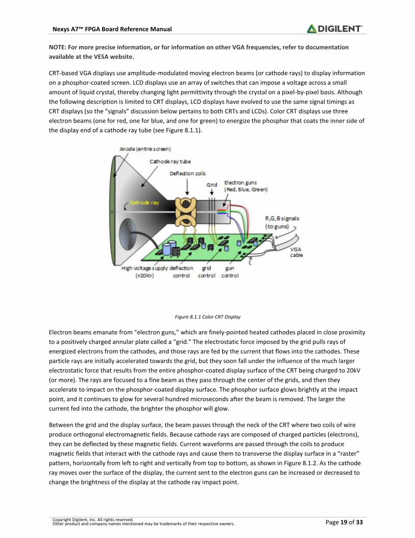
CRT displays (so the “signals” discussion below pertains to both CRTs and LCDs). Color CRT displays use three
electron beams (one for red, one for blue, and one for green) to energize the phosphor that coats the inner side of
the display end of a cathode ray tube (see Figure 8.1.1).
Figure 8.1.1 Color CRT Display
Electron beams emanate from “electron guns,” which are finely-pointed heated cathodes placed in close proximity
to a positively charged annular plate called a “grid.” The electrostatic force imposed by the grid pulls rays of
energized electrons from the cathodes, and those rays are fed by the current that flows into the cathodes. These
particle rays are initially accelerated towards the grid, but they soon fall under the influence of the much larger
electrostatic force that results from the entire phosphor-coated display surface of the CRT being charged to 20kV
(or more). The rays are focused to a fine beam as they pass through the center of the grids, and then they
accelerate to impact on the phosphor-coated display surface. The phosphor surface glows brightly at the impact
point, and it continues to glow for several hundred microseconds after the beam is removed. The larger the
current fed into the cathode, the brighter the phosphor will glow.
Between the grid and the display surface, the beam passes through the neck of the CRT where two coils of wire
produce orthogonal electromagnetic fields. Because cathode rays are composed of charged particles (electrons),
they can be deflected by these magnetic fields. Current waveforms are passed through the coils to produce
magnetic fields that interact with the cathode rays and cause them to transverse the display surface in a “raster”
pattern, horizontally from left to right and vertically from top to bottom, as shown in Figure 8.1.2. As the cathode
ray moves over the surface of the display, the current sent to the electron guns can be increased or decreased to
change the brightness of the display at the cathode ray impact point.
Nexys A7™ FPGA Board Reference Manual
Copyright Digilent, Inc. All rights reserved. Other product and company names mentioned may be trademarks of their respective owners. Page 20 of 33
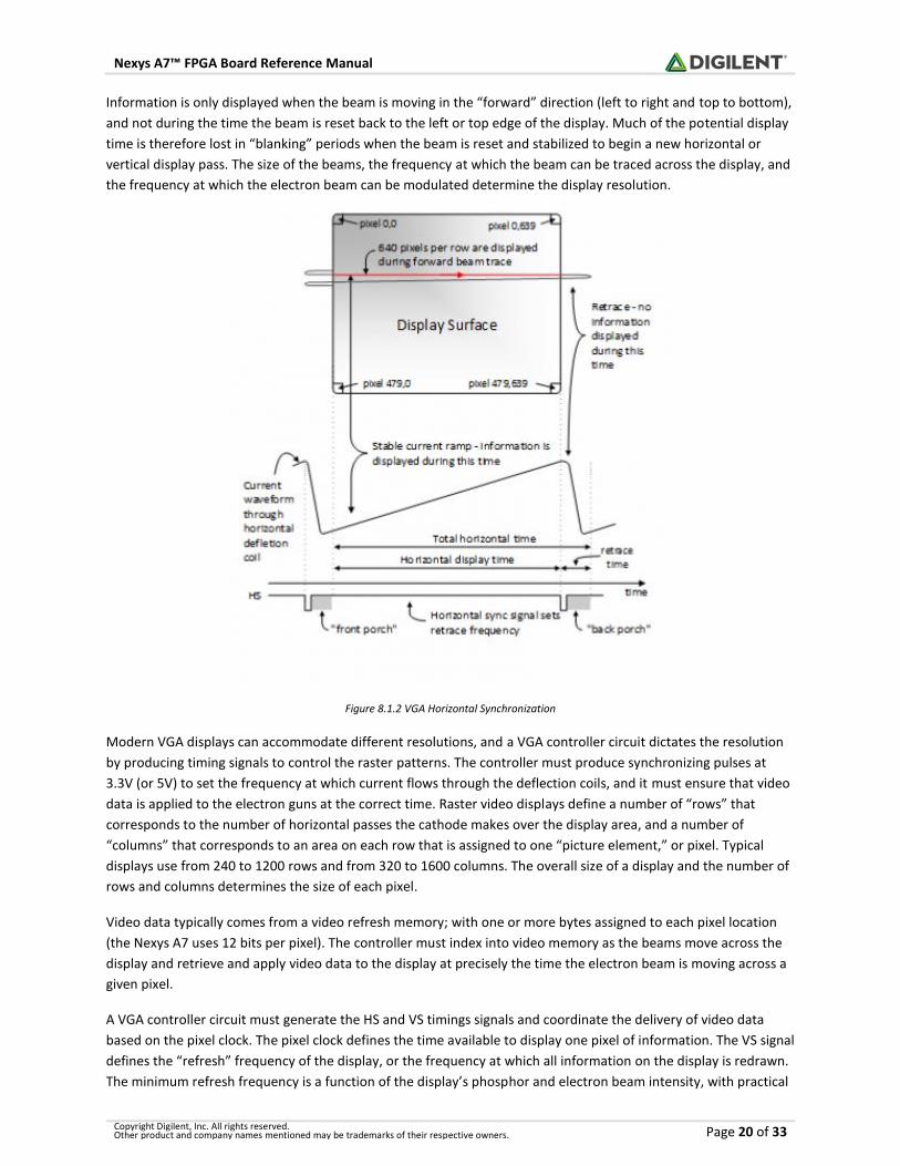
Information is only displayed when the beam is moving in the “forward” direction (left to right and top to bottom),
and not during the time the beam is reset back to the left or top edge of the display. Much of the potential display
time is therefore lost in “blanking” periods when the beam is reset and stabilized to begin a new horizontal or
vertical display pass. The size of the beams, the frequency at which the beam can be traced across the display, and
the frequency at which the electron beam can be modulated determine the display resolution.
Figure 8.1.2 VGA Horizontal Synchronization
Modern VGA displays can accommodate different resolutions, and a VGA controller circuit dictates the resolution
by producing timing signals to control the raster patterns. The controller must produce synchronizing pulses at
3.3V (or 5V) to set the frequency at which current flows through the deflection coils, and it must ensure that video
data is applied to the electron guns at the correct time. Raster video displays define a number of “rows” that
corresponds to the number of horizontal passes the cathode makes over the display area, and a number of
“columns” that corresponds to an area on each row that is assigned to one “picture element,” or pixel. Typical
displays use from 240 to 1200 rows and from 320 to 1600 columns. The overall size of a display and the number of
rows and columns determines the size of each pixel.
Video data typically comes from a video refresh memory; with one or more bytes assigned to each pixel location
(the Nexys A7 uses 12 bits per pixel). The controller must index into video memory as the beams move across the
display and retrieve and apply video data to the display at precisely the time the electron beam is moving across a
given pixel.
A VGA controller circuit must generate the HS and VS timings signals and coordinate the delivery of video data
based on the pixel clock. The pixel clock defines the time available to display one pixel of information. The VS signal
defines the “refresh” frequency of the display, or the frequency at which all information on the display is redrawn.
The minimum refresh frequency is a function of the display’s phosphor and electron beam intensity, with practical
Nexys A7™ FPGA Board Reference Manual
Copyright Digilent, Inc. All rights reserved. Other product and company names mentioned may be trademarks of their respective owners. Page 21 of 33
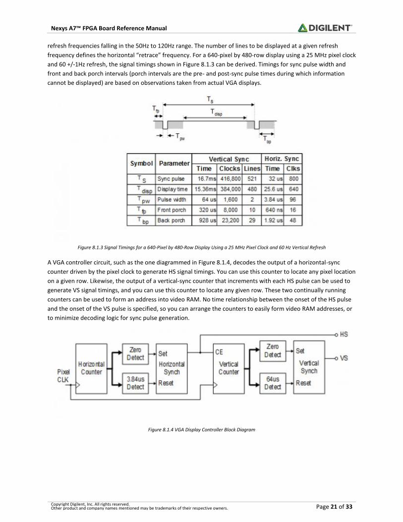
refresh frequencies falling in the 50Hz to 120Hz range. The number of lines to be displayed at a given refresh
frequency defines the horizontal “retrace” frequency. For a 640-pixel by 480-row display using a 25 MHz pixel clock
and 60 +/-1Hz refresh, the signal timings shown in Figure 8.1.3 can be derived. Timings for sync pulse width and
front and back porch intervals (porch intervals are the pre- and post-sync pulse times during which information
cannot be displayed) are based on observations taken from actual VGA displays.
Figure 8.1.3 Signal Timings for a 640-Pixel by 480-Row Display Using a 25 MHz Pixel Clock and 60 Hz Vertical Refresh
A VGA controller circuit, such as the one diagrammed in Figure 8.1.4, decodes the output of a horizontal-sync
counter driven by the pixel clock to generate HS signal timings. You can use this counter to locate any pixel location
on a given row. Likewise, the output of a vertical-sync counter that increments with each HS pulse can be used to
generate VS signal timings, and you can use this counter to locate any given row. These two continually running
counters can be used to form an address into video RAM. No time relationship between the onset of the HS pulse
and the onset of the VS pulse is specified, so you can arrange the counters to easily form video RAM addresses, or
to minimize decoding logic for sync pulse generation.
Figure 8.1.4 VGA Display Controller Block Diagram
Nexys A7™ FPGA Board Reference Manual
Copyright Digilent, Inc. All rights reserved. Other product and company names mentioned may be trademarks of their respective owners. Page 22 of 33
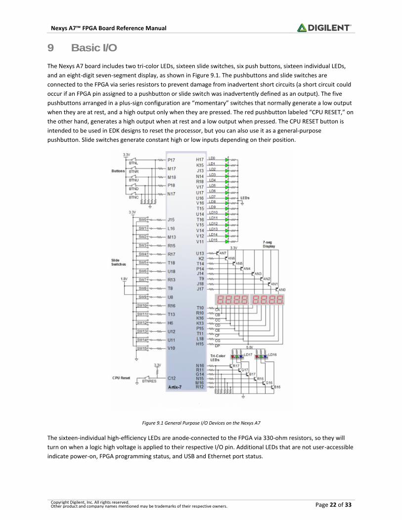
9 Basic I/O
The Nexys A7 board includes two tri-color LEDs, sixteen slide switches, six push buttons, sixteen individual LEDs,
and an eight-digit seven-segment display, as shown in Figure 9.1. The pushbuttons and slide switches are
connected to the FPGA via series resistors to prevent damage from inadvertent short circuits (a short circuit could
occur if an FPGA pin assigned to a pushbutton or slide switch was inadvertently defined as an output). The five
pushbuttons arranged in a plus-sign configuration are “momentary” switches that normally generate a low output
when they are at rest, and a high output only when they are pressed. The red pushbutton labeled “CPU RESET,” on
the other hand, generates a high output when at rest and a low output when pressed. The CPU RESET button is
intended to be used in EDK designs to reset the processor, but you can also use it as a general-purpose
pushbutton. Slide switches generate constant high or low inputs depending on their position.
Figure 9.1 General Purpose I/O Devices on the Nexys A7
The sixteen-individual high-efficiency LEDs are anode-connected to the FPGA via 330-ohm resistors, so they will
turn on when a logic high voltage is applied to their respective I/O pin. Additional LEDs that are not user-accessible
indicate power-on, FPGA programming status, and USB and Ethernet port status.
Nexys A7™ FPGA Board Reference Manual
Copyright Digilent, Inc. All rights reserved. Other product and company names mentioned may be trademarks of their respective owners. Page 23 of 33
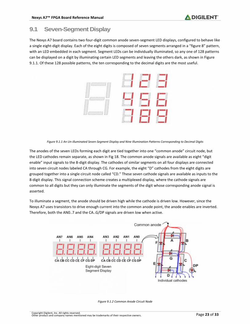
9.1 Seven-Segment Display
The Nexys A7 board contains two four-digit common anode seven-segment LED displays, configured to behave like
a single eight-digit display. Each of the eight digits is composed of seven segments arranged in a “figure 8” pattern,
with an LED embedded in each segment. Segment LEDs can be individually illuminated, so any one of 128 patterns
can be displayed on a digit by illuminating certain LED segments and leaving the others dark, as shown in Figure
9.1.1. Of these 128 possible patterns, the ten corresponding to the decimal digits are the most useful.
Figure 9.1.1 An Un-illuminated Seven-Segment Display and Nine Illumination Patterns Corresponding to Decimal Digits
The anodes of the seven LEDs forming each digit are tied together into one “common anode” circuit node, but
the LED cathodes remain separate, as shown in Fig 18. The common anode signals are available as eight “digit
enable” input signals to the 8-digit display. The cathodes of similar segments on all four displays are connected
into seven circuit nodes labeled CA through CG. For example, the eight “D” cathodes from the eight digits are
grouped together into a single circuit node called “CD.” These seven cathode signals are available as inputs to the
8-digit display. This signal connection scheme creates a multiplexed display, where the cathode signals are
common to all digits but they can only illuminate the segments of the digit whose corresponding anode signal is
asserted.
To illuminate a segment, the anode should be driven high while the cathode is driven low. However, since the
Nexys A7 uses transistors to drive enough current into the common anode point, the anode enables are inverted.
Therefore, both the AN0..7 and the CA..G/DP signals are driven low when active.
Figure 9.1.2 Common Anode Circuit Node
Nexys A7™ FPGA Board Reference Manual
Copyright Digilent, Inc. All rights reserved. Other product and company names mentioned may be trademarks of their respective owners. Page 24 of 33
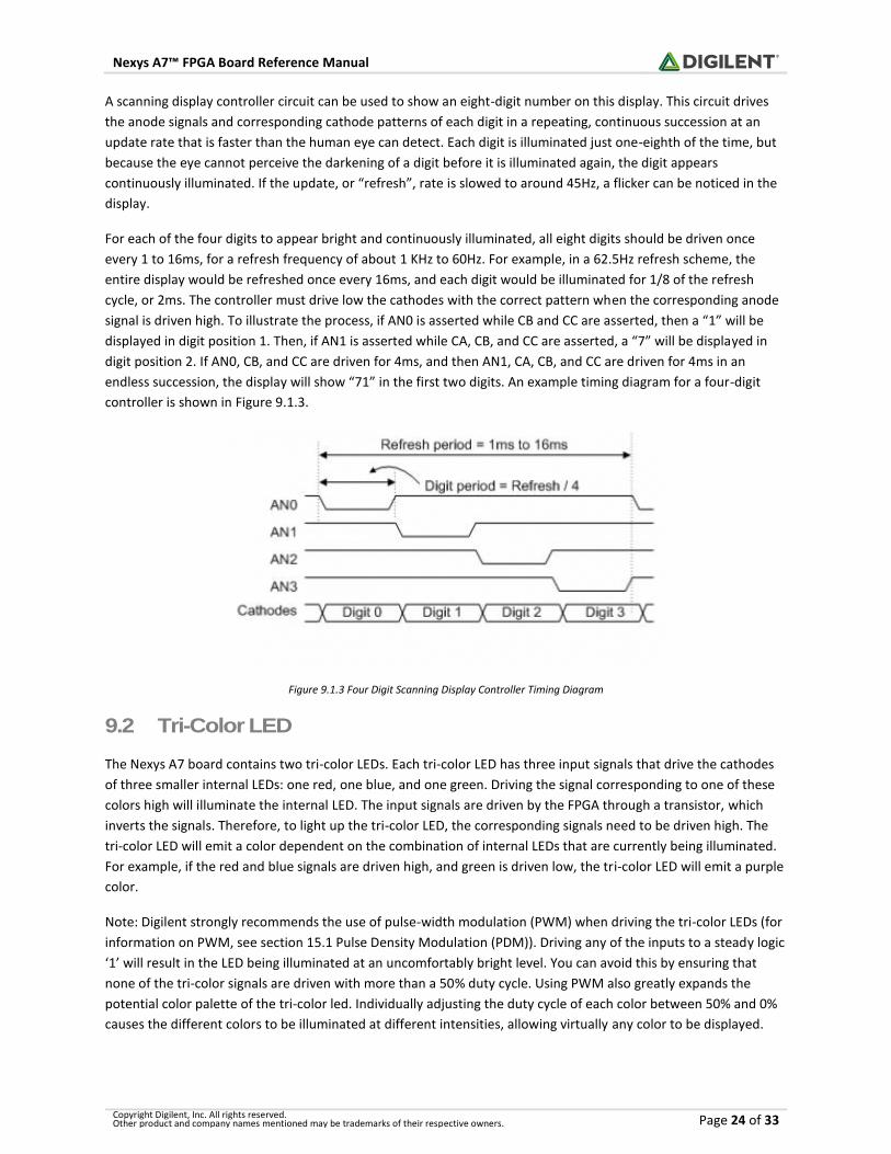
A scanning display controller circuit can be used to show an eight-digit number on this display. This circuit drives
the anode signals and corresponding cathode patterns of each digit in a repeating, continuous succession at an
update rate that is faster than the human eye can detect. Each digit is illuminated just one-eighth of the time, but
because the eye cannot perceive the darkening of a digit before it is illuminated again, the digit appears
continuously illuminated. If the update, or “refresh”, rate is slowed to around 45Hz, a flicker can be noticed in the
display.
For each of the four digits to appear bright and continuously illuminated, all eight digits should be driven once
every 1 to 16ms, for a refresh frequency of about 1 KHz to 60Hz. For example, in a 62.5Hz refresh scheme, the
entire display would be refreshed once every 16ms, and each digit would be illuminated for 1/8 of the refresh
cycle, or 2ms. The controller must drive low the cathodes with the correct pattern when the corresponding anode
signal is driven high. To illustrate the process, if AN0 is asserted while CB and CC are asserted, then a “1” will be
displayed in digit position 1. Then, if AN1 is asserted while CA, CB, and CC are asserted, a “7” will be displayed in
digit position 2. If AN0, CB, and CC are driven for 4ms, and then AN1, CA, CB, and CC are driven for 4ms in an
endless succession, the display will show “71” in the first two digits. An example timing diagram for a four-digit
controller is shown in Figure 9.1.3.
Figure 9.1.3 Four Digit Scanning Display Controller Timing Diagram
9.2 Tri-Color LED
The Nexys A7 board contains two tri-color LEDs. Each tri-color LED has three input signals that drive the cathodes
of three smaller internal LEDs: one red, one blue, and one green. Driving the signal corresponding to one of these
colors high will illuminate the internal LED. The input signals are driven by the FPGA through a transistor, which
inverts the signals. Therefore, to light up the tri-color LED, the corresponding signals need to be driven high. The
tri-color LED will emit a color dependent on the combination of internal LEDs that are currently being illuminated.
For example, if the red and blue signals are driven high, and green is driven low, the tri-color LED will emit a purple
color.
Note: Digilent strongly recommends the use of pulse-width modulation (PWM) when driving the tri-color LEDs (for
information on PWM, see section 15.1 Pulse Density Modulation (PDM)). Driving any of the inputs to a steady logic
‘1’ will result in the LED being illuminated at an uncomfortably bright level. You can avoid this by ensuring that
none of the tri-color signals are driven with more than a 50% duty cycle. Using PWM also greatly expands the
potential color palette of the tri-color led. Individually adjusting the duty cycle of each color between 50% and 0%
causes the different colors to be illuminated at different intensities, allowing virtually any color to be displayed.
Nexys A7™ FPGA Board Reference Manual
Copyright Digilent, Inc. All rights reserved. Other product and company names mentioned may be trademarks of their respective owners. Page 25 of 33
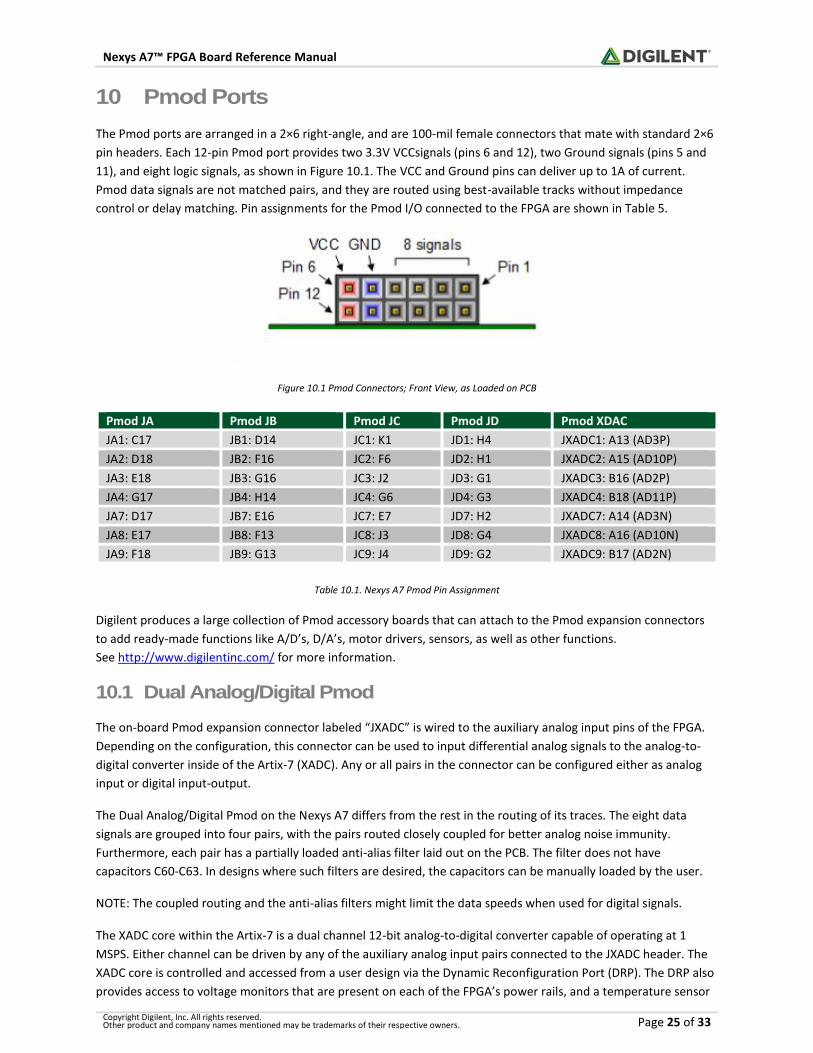
10 Pmod Ports
The Pmod ports are arranged in a 2×6 right-angle, and are 100-mil female connectors that mate with standard 2×6
pin headers. Each 12-pin Pmod port provides two 3.3V VCCsignals (pins 6 and 12), two Ground signals (pins 5 and
11), and eight logic signals, as shown in Figure 10.1. The VCC and Ground pins can deliver up to 1A of current.
Pmod data signals are not matched pairs, and they are routed using best-available tracks without impedance
control or delay matching. Pin assignments for the Pmod I/O connected to the FPGA are shown in Table 5.
Figure 10.1 Pmod Connectors; Front View, as Loaded on PCB
Pmod JA Pmod JB Pmod JC Pmod JD Pmod XDAC
JA1: C17 JB1: D14 JC1: K1 JD1: H4 JXADC1: A13 (AD3P)
JA2: D18 JB2: F16 JC2: F6 JD2: H1 JXADC2: A15 (AD10P)
JA3: E18 JB3: G16 JC3: J2 JD3: G1 JXADC3: B16 (AD2P)
JA4: G17 JB4: H14 JC4: G6 JD4: G3 JXADC4: B18 (AD11P)
JA7: D17 JB7: E16 JC7: E7 JD7: H2 JXADC7: A14 (AD3N)
JA8: E17 JB8: F13 JC8: J3 JD8: G4 JXADC8: A16 (AD10N)
JA9: F18 JB9: G13 JC9: J4 JD9: G2 JXADC9: B17 (AD2N)
Table 10.1. Nexys A7 Pmod Pin Assignment
Digilent produces a large collection of Pmod accessory boards that can attach to the Pmod expansion connectors
to add ready-made functions like A/D’s, D/A’s, motor drivers, sensors, as well as other functions.
See http://www.digilentinc.com/ for more information.
10.1 Dual Analog/Digital Pmod
The on-board Pmod expansion connector labeled “JXADC” is wired to the auxiliary analog input pins of the FPGA.
Depending on the configuration, this connector can be used to input differential analog signals to the analog-to-
digital converter inside of the Artix-7 (XADC). Any or all pairs in the connector can be configured either as analog
input or digital input-output.
The Dual Analog/Digital Pmod on the Nexys A7 differs from the rest in the routing of its traces. The eight data
signals are grouped into four pairs, with the pairs routed closely coupled for better analog noise immunity.
Furthermore, each pair has a partially loaded anti-alias filter laid out on the PCB. The filter does not have
capacitors C60-C63. In designs where such filters are desired, the capacitors can be manually loaded by the user.
NOTE: The coupled routing and the anti-alias filters might limit the data speeds when used for digital signals.
The XADC core within the Artix-7 is a dual channel 12-bit analog-to-digital converter capable of operating at 1
MSPS. Either channel can be driven by any of the auxiliary analog input pairs connected to the JXADC header. The
XADC core is controlled and accessed from a user design via the Dynamic Reconfiguration Port (DRP). The DRP also
provides access to voltage monitors that are present on each of the FPGA’s power rails, and a temperature sensor
Nexys A7™ FPGA Board Reference Manual
Copyright Digilent, Inc. All rights reserved. Other product and company names mentioned may be trademarks of their respective owners. Page 26 of 33
that is internal to the FPGA. For more information on using the XADC core, refer to the Xilinx document titled “7
Series FPGAs and Zynq-7000 All Programmable SoC XADC Dual 12-Bit 1 MSPS Analog-to-Digital Converter.”
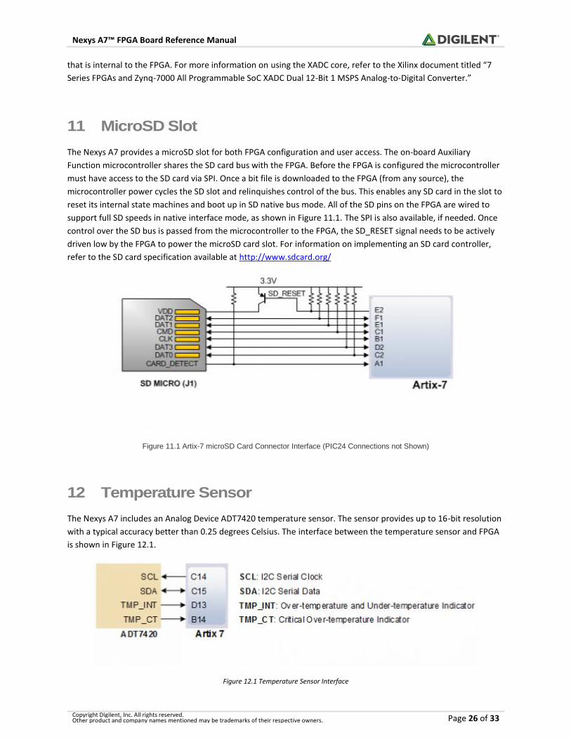
11 MicroSD Slot
The Nexys A7 provides a microSD slot for both FPGA configuration and user access. The on-board Auxiliary
Function microcontroller shares the SD card bus with the FPGA. Before the FPGA is configured the microcontroller
must have access to the SD card via SPI. Once a bit file is downloaded to the FPGA (from any source), the
microcontroller power cycles the SD slot and relinquishes control of the bus. This enables any SD card in the slot to
reset its internal state machines and boot up in SD native bus mode. All of the SD pins on the FPGA are wired to
support full SD speeds in native interface mode, as shown in Figure 11.1. The SPI is also available, if needed. Once
control over the SD bus is passed from the microcontroller to the FPGA, the SD_RESET signal needs to be actively
driven low by the FPGA to power the microSD card slot. For information on implementing an SD card controller,
refer to the SD card specification available at http://www.sdcard.org/
Figure 11.1 Artix-7 microSD Card Connector Interface (PIC24 Connections not Shown)
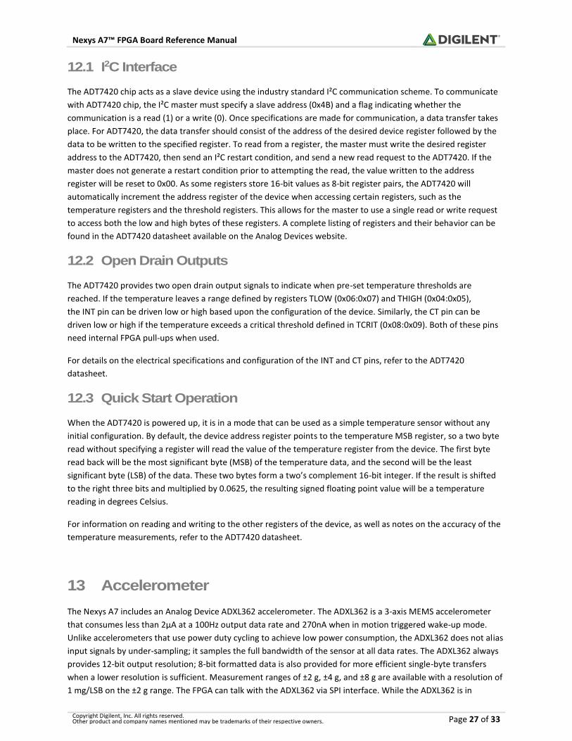
12 Temperature Sensor
The Nexys A7 includes an Analog Device ADT7420 temperature sensor. The sensor provides up to 16-bit resolution
with a typical accuracy better than 0.25 degrees Celsius. The interface between the temperature sensor and FPGA
is shown in Figure 12.1.
Figure 12.1 Temperature Sensor Interface
Nexys A7™ FPGA Board Reference Manual
Copyright Digilent, Inc. All rights reserved. Other product and company names mentioned may be trademarks of their respective owners. Page 27 of 33
12.1 I2C Interface
The ADT7420 chip acts as a slave device using the industry standard I²C communication scheme. To communicate
with ADT7420 chip, the I²C master must specify a slave address (0x4B) and a flag indicating whether the
communication is a read (1) or a write (0). Once specifications are made for communication, a data transfer takes
place. For ADT7420, the data transfer should consist of the address of the desired device register followed by the
data to be written to the specified register. To read from a register, the master must write the desired register
address to the ADT7420, then send an I²C restart condition, and send a new read request to the ADT7420. If the
master does not generate a restart condition prior to attempting the read, the value written to the address
register will be reset to 0x00. As some registers store 16-bit values as 8-bit register pairs, the ADT7420 will
automatically increment the address register of the device when accessing certain registers, such as the
temperature registers and the threshold registers. This allows for the master to use a single read or write request
to access both the low and high bytes of these registers. A complete listing of registers and their behavior can be
found in the ADT7420 datasheet available on the Analog Devices website.
12.2 Open Drain Outputs
The ADT7420 provides two open drain output signals to indicate when pre-set temperature thresholds are
reached. If the temperature leaves a range defined by registers TLOW (0x06:0x07) and THIGH (0x04:0x05),
the INT pin can be driven low or high based upon the configuration of the device. Similarly, the CT pin can be
driven low or high if the temperature exceeds a critical threshold defined in TCRIT (0x08:0x09). Both of these pins
need internal FPGA pull-ups when used.
For details on the electrical specifications and configuration of the INT and CT pins, refer to the ADT7420
datasheet.
12.3 Quick Start Operation
When the ADT7420 is powered up, it is in a mode that can be used as a simple temperature sensor without any
initial configuration. By default, the device address register points to the temperature MSB register, so a two byte
read without specifying a register will read the value of the temperature register from the device. The first byte
read back will be the most significant byte (MSB) of the temperature data, and the second will be the least
significant byte (LSB) of the data. These two bytes form a two’s complement 16-bit integer. If the result is shifted
to the right three bits and multiplied by 0.0625, the resulting signed floating point value will be a temperature
reading in degrees Celsius.
For information on reading and writing to the other registers of the device, as well as notes on the accuracy of the
temperature measurements, refer to the ADT7420 datasheet.
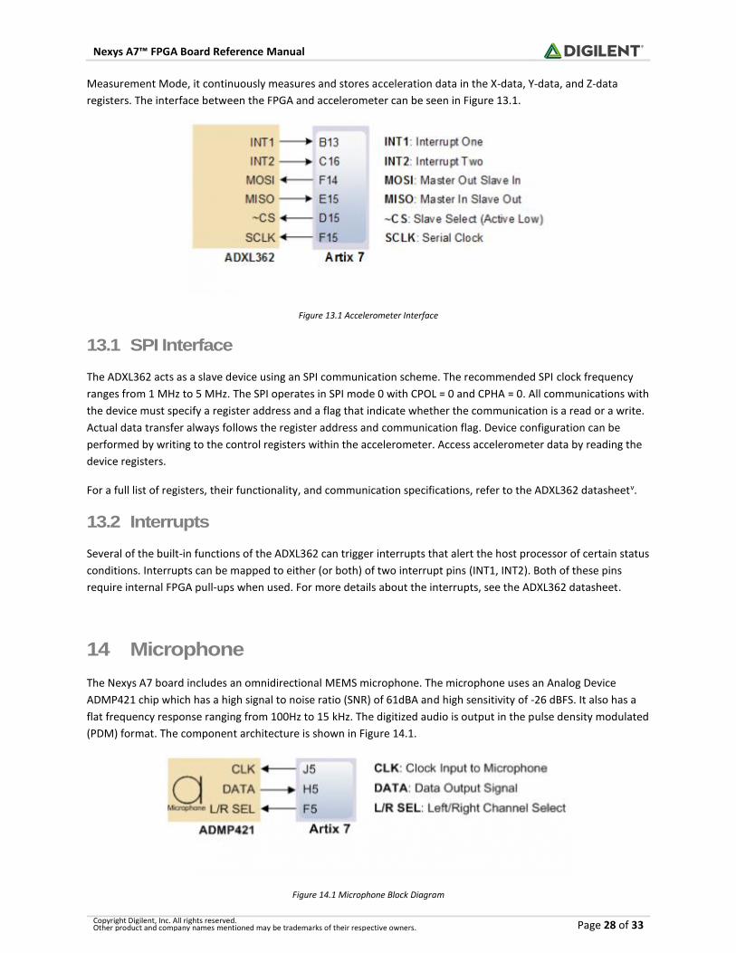
13 Accelerometer
The Nexys A7 includes an Analog Device ADXL362 accelerometer. The ADXL362 is a 3-axis MEMS accelerometer
that consumes less than 2μA at a 100Hz output data rate and 270nA when in motion triggered wake-up mode.
Unlike accelerometers that use power duty cycling to achieve low power consumption, the ADXL362 does not alias
input signals by under-sampling; it samples the full bandwidth of the sensor at all data rates. The ADXL362 always
provides 12-bit output resolution; 8-bit formatted data is also provided for more efficient single-byte transfers
when a lower resolution is sufficient. Measurement ranges of ±2 g, ±4 g, and ±8 g are available with a resolution of
1 mg/LSB on the ±2 g range. The FPGA can talk with the ADXL362 via SPI interface. While the ADXL362 is in
Nexys A7™ FPGA Board Reference Manual
Copyright Digilent, Inc. All rights reserved. Other product and company names mentioned may be trademarks of their respective owners. Page 28 of 33
Measurement Mode, it continuously measures and stores acceleration data in the X-data, Y-data, and Z-data
registers. The interface between the FPGA and accelerometer can be seen in Figure 13.1.
Figure 13.1 Accelerometer Interface
13.1 SPI Interface
The ADXL362 acts as a slave device using an SPI communication scheme. The recommended SPI clock frequency
ranges from 1 MHz to 5 MHz. The SPI operates in SPI mode 0 with CPOL = 0 and CPHA = 0. All communications with
the device must specify a register address and a flag that indicate whether the communication is a read or a write.
Actual data transfer always follows the register address and communication flag. Device configuration can be
performed by writing to the control registers within the accelerometer. Access accelerometer data by reading the
device registers.
For a full list of registers, their functionality, and communication specifications, refer to the ADXL362 datasheetv.
13.2 Interrupts
Several of the built-in functions of the ADXL362 can trigger interrupts that alert the host processor of certain status
conditions. Interrupts can be mapped to either (or both) of two interrupt pins (INT1, INT2). Both of these pins
require internal FPGA pull-ups when used. For more details about the interrupts, see the ADXL362 datasheet.
14 Microphone
The Nexys A7 board includes an omnidirectional MEMS microphone. The microphone uses an Analog Device
ADMP421 chip which has a high signal to noise ratio (SNR) of 61dBA and high sensitivity of -26 dBFS. It also has a
flat frequency response ranging from 100Hz to 15 kHz. The digitized audio is output in the pulse density modulated
(PDM) format. The component architecture is shown in Figure 14.1.
Figure 14.1 Microphone Block Diagram
Nexys A7™ FPGA Board Reference Manual
Copyright Digilent, Inc. All rights reserved. Other product and company names mentioned may be trademarks of their respective owners. Page 29 of 33
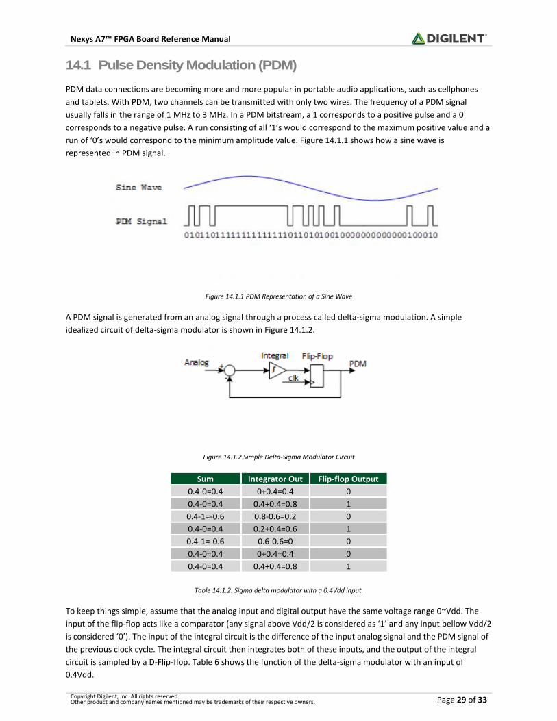
14.1 Pulse Density Modulation (PDM)
PDM data connections are becoming more and more popular in portable audio applications, such as cellphones
and tablets. With PDM, two channels can be transmitted with only two wires. The frequency of a PDM signal
usually falls in the range of 1 MHz to 3 MHz. In a PDM bitstream, a 1 corresponds to a positive pulse and a 0
corresponds to a negative pulse. A run consisting of all ‘1’s would correspond to the maximum positive value and a
run of ‘0’s would correspond to the minimum amplitude value. Figure 14.1.1 shows how a sine wave is
represented in PDM signal.
Figure 14.1.1 PDM Representation of a Sine Wave
A PDM signal is generated from an analog signal through a process called delta-sigma modulation. A simple
idealized circuit of delta-sigma modulator is shown in Figure 14.1.2.
Figure 14.1.2 Simple Delta-Sigma Modulator Circuit
Sum Integrator Out Flip-flop Output
0.4-0=0.4 0+0.4=0.4 0
0.4-0=0.4 0.4+0.4=0.8 1
0.4-1=-0.6 0.8-0.6=0.2 0
0.4-0=0.4 0.2+0.4=0.6 1
0.4-1=-0.6 0.6-0.6=0 0
0.4-0=0.4 0+0.4=0.4 0
0.4-0=0.4 0.4+0.4=0.8 1
Table 14.1.2. Sigma delta modulator with a 0.4Vdd input.
To keep things simple, assume that the analog input and digital output have the same voltage range 0~Vdd. The
input of the flip-flop acts like a comparator (any signal above Vdd/2 is considered as ‘1’ and any input bellow Vdd/2
is considered ‘0’). The input of the integral circuit is the difference of the input analog signal and the PDM signal of
the previous clock cycle. The integral circuit then integrates both of these inputs, and the output of the integral
circuit is sampled by a D-Flip-flop. Table 6 shows the function of the delta-sigma modulator with an input of
0.4Vdd.
Nexys A7™ FPGA Board Reference Manual
Copyright Digilent, Inc. All rights reserved. Other product and company names mentioned may be trademarks of their respective owners. Page 30 of 33
Note that the average of the flip-flop output equals the value of the input analog signal. So in order to get the
value of analog input, all that is needed is a counter that counts the ‘1’s for a certain period of time.
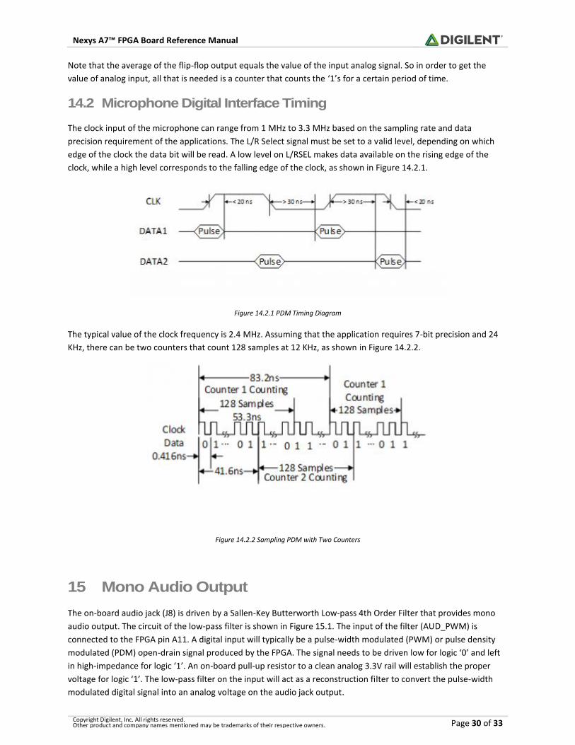
14.2 Microphone Digital Interface Timing
The clock input of the microphone can range from 1 MHz to 3.3 MHz based on the sampling rate and data
precision requirement of the applications. The L/R Select signal must be set to a valid level, depending on which
edge of the clock the data bit will be read. A low level on L/RSEL makes data available on the rising edge of the
clock, while a high level corresponds to the falling edge of the clock, as shown in Figure 14.2.1.
Figure 14.2.1 PDM Timing Diagram
The typical value of the clock frequency is 2.4 MHz. Assuming that the application requires 7-bit precision and 24
KHz, there can be two counters that count 128 samples at 12 KHz, as shown in Figure 14.2.2.
Figure 14.2.2 Sampling PDM with Two Counters
15 Mono Audio Output
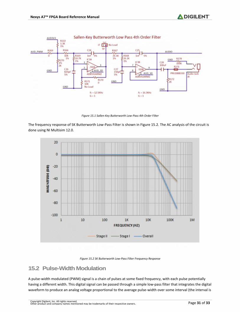
The on-board audio jack (J8) is driven by a Sallen-Key Butterworth Low-pass 4th Order Filter that provides mono
audio output. The circuit of the low-pass filter is shown in Figure 15.1. The input of the filter (AUD_PWM) is
connected to the FPGA pin A11. A digital input will typically be a pulse-width modulated (PWM) or pulse density
modulated (PDM) open-drain signal produced by the FPGA. The signal needs to be driven low for logic ‘0’ and left
in high-impedance for logic ‘1’. An on-board pull-up resistor to a clean analog 3.3V rail will establish the proper
voltage for logic ‘1’. The low-pass filter on the input will act as a reconstruction filter to convert the pulse-width
modulated digital signal into an analog voltage on the audio jack output.
Nexys A7™ FPGA Board Reference Manual
Copyright Digilent, Inc. All rights reserved. Other product and company names mentioned may be trademarks of their respective owners. Page 31 of 33
Figure 15.1 Sallen-Key Butterworth Low-Pass 4th Order Filter
The frequency response of SK Butterworth Low-Pass Filter is shown in Figure 15.2. The AC analysis of the circuit is
done using NI Multisim 12.0.
Figure 15.2 SK Butterworth Low-Pass Filter Frequency Response
15.2 Pulse-Width Modulation
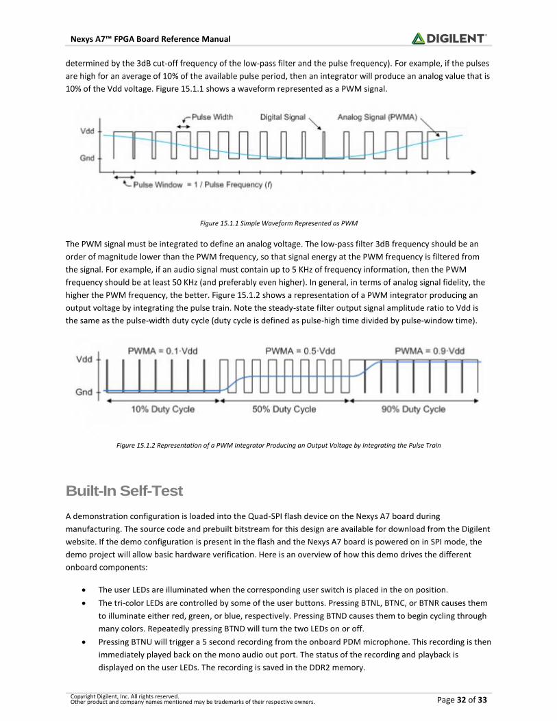
A pulse-width modulated (PWM) signal is a chain of pulses at some fixed frequency, with each pulse potentially
having a different width. This digital signal can be passed through a simple low-pass filter that integrates the digital
waveform to produce an analog voltage proportional to the average pulse-width over some interval (the interval is
Nexys A7™ FPGA Board Reference Manual
Copyright Digilent, Inc. All rights reserved. Other product and company names mentioned may be trademarks of their respective owners. Page 32 of 33
determined by the 3dB cut-off frequency of the low-pass filter and the pulse frequency). For example, if the pulses
are high for an average of 10% of the available pulse period, then an integrator will produce an analog value that is
10% of the Vdd voltage. Figure 15.1.1 shows a waveform represented as a PWM signal.
Figure 15.1.1 Simple Waveform Represented as PWM
The PWM signal must be integrated to define an analog voltage. The low-pass filter 3dB frequency should be an
order of magnitude lower than the PWM frequency, so that signal energy at the PWM frequency is filtered from
the signal. For example, if an audio signal must contain up to 5 KHz of frequency information, then the PWM
frequency should be at least 50 KHz (and preferably even higher). In general, in terms of analog signal fidelity, the
higher the PWM frequency, the better. Figure 15.1.2 shows a representation of a PWM integrator producing an
output voltage by integrating the pulse train. Note the steady-state filter output signal amplitude ratio to Vdd is
the same as the pulse-width duty cycle (duty cycle is defined as pulse-high time divided by pulse-window time).
Figure 15.1.2 Representation of a PWM Integrator Producing an Output Voltage by Integrating the Pulse Train
Built-In Self-Test
A demonstration configuration is loaded into the Quad-SPI flash device on the Nexys A7 board during
manufacturing. The source code and prebuilt bitstream for this design are available for download from the Digilent
website. If the demo configuration is present in the flash and the Nexys A7 board is powered on in SPI mode, the
demo project will allow basic hardware verification. Here is an overview of how this demo drives the different
onboard components:
• The user LEDs are illuminated when the corresponding user switch is placed in the on position.
• The tri-color LEDs are controlled by some of the user buttons. Pressing BTNL, BTNC, or BTNR causes them
to illuminate either red, green, or blue, respectively. Pressing BTND causes them to begin cycling through
many colors. Repeatedly pressing BTND will turn the two LEDs on or off.
• Pressing BTNU will trigger a 5 second recording from the onboard PDM microphone. This recording is then
immediately played back on the mono audio out port. The status of the recording and playback is
displayed on the user LEDs. The recording is saved in the DDR2 memory.
Nexys A7™ FPGA Board Reference Manual
Copyright Digilent, Inc. All rights reserved. Other product and company names mentioned may be trademarks of their respective owners. Page 33 of 33
• The VGA port displays feedback from the onboard microphone, temperature sensors, accelerometer, RGB
LEDs, and USB Mouse.
• Connecting a mouse to the USB-HID Mouse port will allow the pointer on the VGA display to be
controlled. Only mice compatible with the Boot Mouse HID interface are supported.
• The seven-segment display will display a moving snake pattern.
All Nexys A7 boards are 100% tested during the manufacturing process. If any device on the Nexys A7 board fails
test or is not responding properly, it is likely that damage occurred during transport or during use. Typical damage
includes stressed solder joints and contaminants in switches and buttons resulting in intermittent failures. Stressed
solder joints can be repaired by reheating and reflowing solder and contaminants can be cleaned with off-the-shelf
electronics cleaning products. If a board fails test within the warranty period, it will be replaced at no cost. Contact
Digilent for more details.
i Zynq-7000 SoC and 7 Series Devices Memory Interface Solutions from Xilinx ii Spansion S25FL032P_00 Datasheet iii 7-Series FPGAs Configuration User Guide from Xilinx iv SMSC LAN8720A Datasheet from Microchip v ADXL362 Product Page from Analog Devices