Embed Size (px)
DESCRIPTION
New Pipeline DAQ and 12GeV Trigger Systems. R. Chris Cuevas Group Leader – Fast Electronics. Hall C Summer Workshop Jefferson Lab 15-August-2013. OUTLINE. Overview - DAQ and Trigger design requirements Before Pipeline – The Classic method of DAQ - PowerPoint PPT Presentation
Citation preview
Thomas Jefferson National Accelerator Facility
IPR Nov 27-29, 2012Page 1
New Pipeline DAQand
12GeV Trigger Systems
R. Chris CuevasGroup Leader – Fast Electronics
Hall C Summer WorkshopJefferson Lab
15-August-2013
Thomas Jefferson National Accelerator Facility
IPR Nov 27-29, 2012Page 2
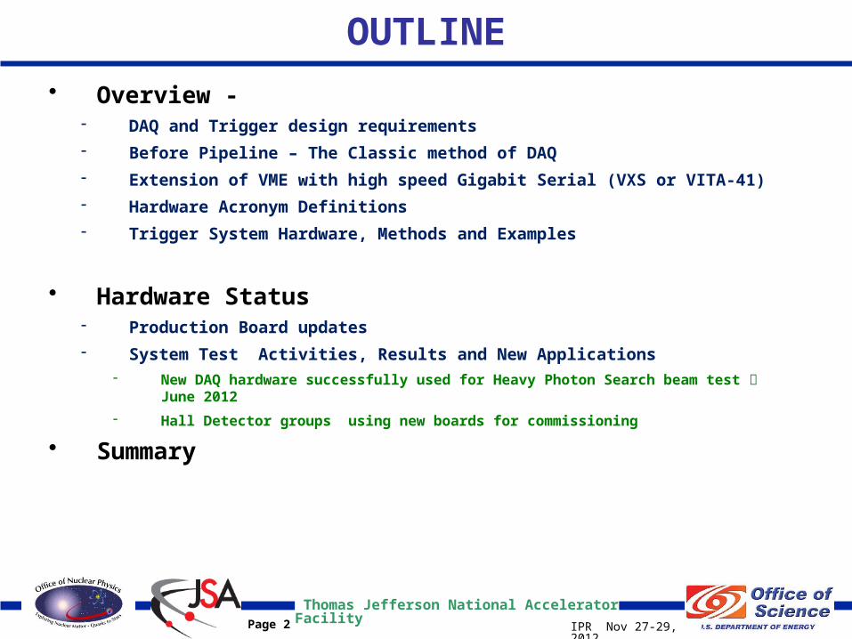
OUTLINE
• Overview - - DAQ and Trigger design requirements
- Before Pipeline – The Classic method of DAQ
- Extension of VME with high speed Gigabit Serial (VXS or VITA-41)
- Hardware Acronym Definitions
- Trigger System Hardware, Methods and Examples
• Hardware Status- Production Board updates
- System Test Activities, Results and New Applications- New DAQ hardware successfully used for Heavy Photon Search beam test June 2012
- Hall Detector groups using new boards for commissioning
• Summary
Thomas Jefferson National Accelerator Facility
IPR Nov 27-29, 2012Page 3
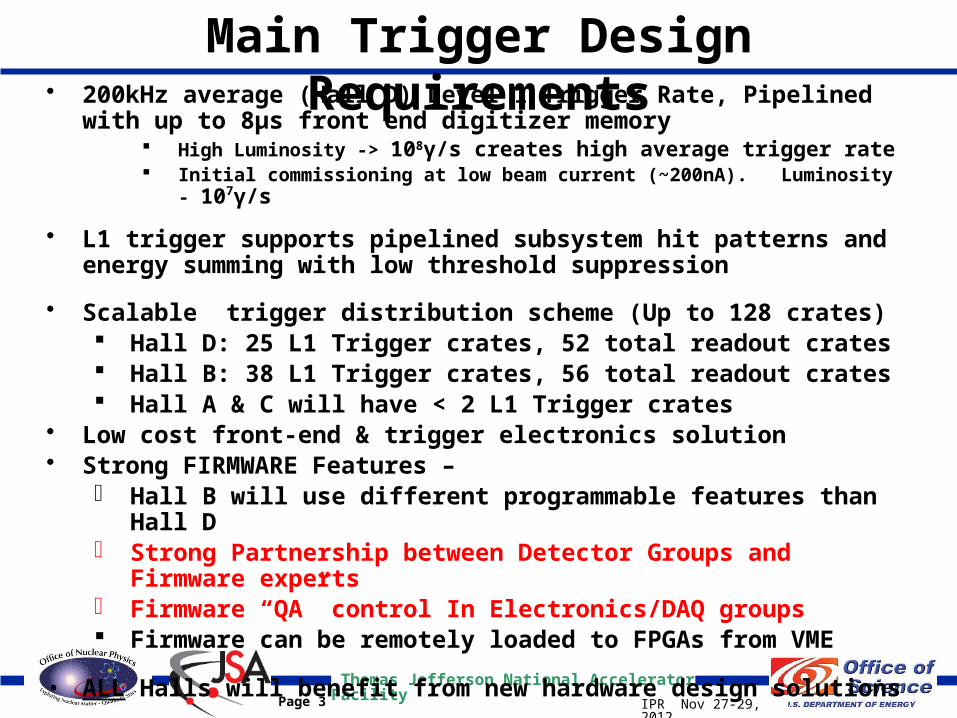
Main Trigger Design Requirements• 200kHz average (Hall D) Level 1 Trigger Rate, Pipelined with up to 8µs
front end digitizer memory High Luminosity -> 108γ/s creates high average trigger rate Initial commissioning at low beam current (~200nA). Luminosity - 107γ/s
• L1 trigger supports pipelined subsystem hit patterns and energy summing with low threshold suppression
• Scalable trigger distribution scheme (Up to 128 crates) Hall D: 25 L1 Trigger crates, 52 total readout crates Hall B: 38 L1 Trigger crates, 56 total readout crates Hall A & C will have < 2 L1 Trigger crates
• Low cost front-end & trigger electronics solution• Strong FIRMWARE Features –
- Hall B will use different programmable features than Hall D- Strong Partnership between Detector Groups and Firmware experts- Firmware “QA” control In Electronics/DAQ groups Firmware can be remotely loaded to FPGAs from VME
• ALL Halls will benefit from new hardware design solutions
Thomas Jefferson National Accelerator Facility
IPR Nov 27-29, 2012Page 4
SplitterQDC
Discriminator
Delay line
TDC
to primitivetrigger logic
detectorsignal
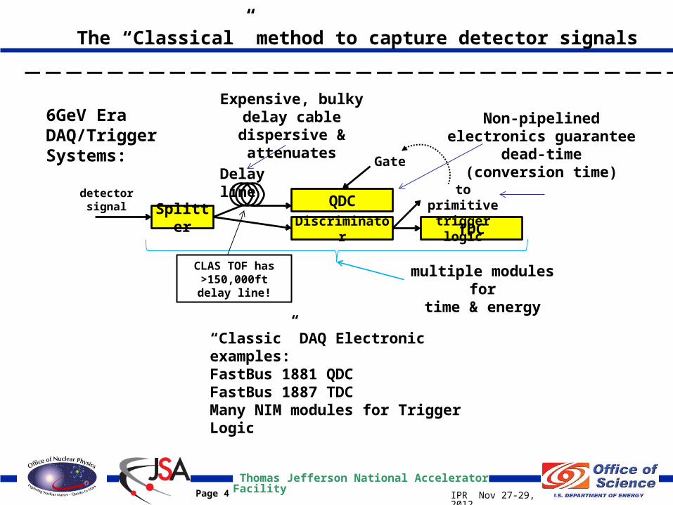
6GeV Era DAQ/TriggerSystems:
Expensive, bulky delay cabledispersive & attenuates
multiple modules fortime & energy
Non-pipelined electronics guarantee dead-time
(conversion time)
CLAS TOF has >150,000ft delay
line!
Gate
The “Classical” method to capture detector signals
“Classic” DAQ Electronic examples:FastBus 1881 QDCFastBus 1887 TDCMany NIM modules for Trigger Logic
Thomas Jefferson National Accelerator Facility
IPR Nov 27-29, 2012Page 5
Energy & Time AlgorithmsEvent #1 Event #2
VMEReadout
FADC12-bit
Trigger #1 Trigger #2
ADC Sample Pipeline
Trigger PulsePre-Processing
GigabitSerial
TriggerData
Physics‘Event’Trigger Input
detectorsignal
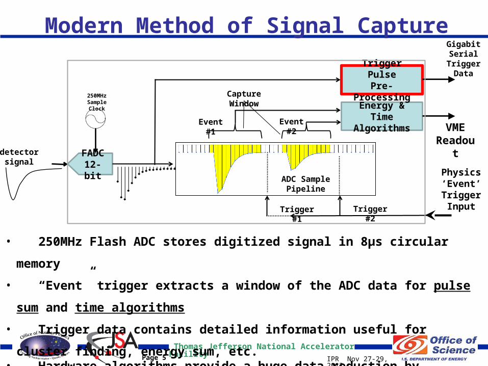
Modern Method of Signal Capture
• 250MHz Flash ADC stores digitized signal in 8μs circular memory
• “Event” trigger extracts a window of the ADC data for pulse sum and time
algorithms
• Trigger data contains detailed information useful for cluster finding, energy sum, etc.• Hardware algorithms provide a huge data reduction by reporting only time & energyestimates for readout instead of raw samples
250MHzSample Clock
Capture Window
Thomas Jefferson National Accelerator Facility
IPR Nov 27-29, 2012Page 6
Acronym Definitions
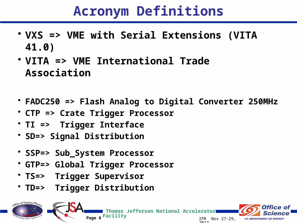
• VXS => VME with Serial Extensions (VITA 41.0)• VITA => VME International Trade Association
• FADC250 => Flash Analog to Digital Converter 250MHz• CTP => Crate Trigger Processor• TI => Trigger Interface• SD=> Signal Distribution
• SSP=> Sub_System Processor• GTP=> Global Trigger Processor• TS=> Trigger Supervisor• TD=> Trigger Distribution
Thomas Jefferson National Accelerator Facility
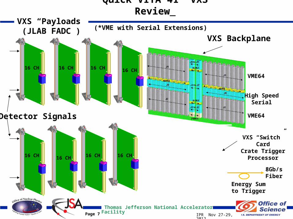
IPR Nov 27-29, 2012Page 7
VXS Backplane
VXS “Switch” CardCrate Trigger
Processor
VXS “Payloads”(JLAB FADC )
VME64
High SpeedSerial
VME64
16 CH
16 CH16 CH16 CH16 CH
16 CH 16 CH 16 CH
Detector Signals
Energy Sum to Trigger
Quick VITA 41 *VXS Review
8Gb/sFiber
(*VME with Serial Extensions)
Thomas Jefferson National Accelerator Facility
IPR Nov 27-29, 2012Page 8
Trigger System Diagram
Crate Trigger Processing
Flash ADC Modules
Detector Signals
Sub-System Processing(Multi-Crate)
Global Trigger Processing
TriggerSupervisor
(Distribution)
TS -> TD -> TILink
1.25Gb/sBi-Directional
BUSYTrigger SyncTrig_Comnd
CTP -> SSP -> GTPL1 Trig_Data
Uni_Directional
Energy Sums
Thomas Jefferson National Accelerator Facility
IPR Nov 27-29, 2012Page 9
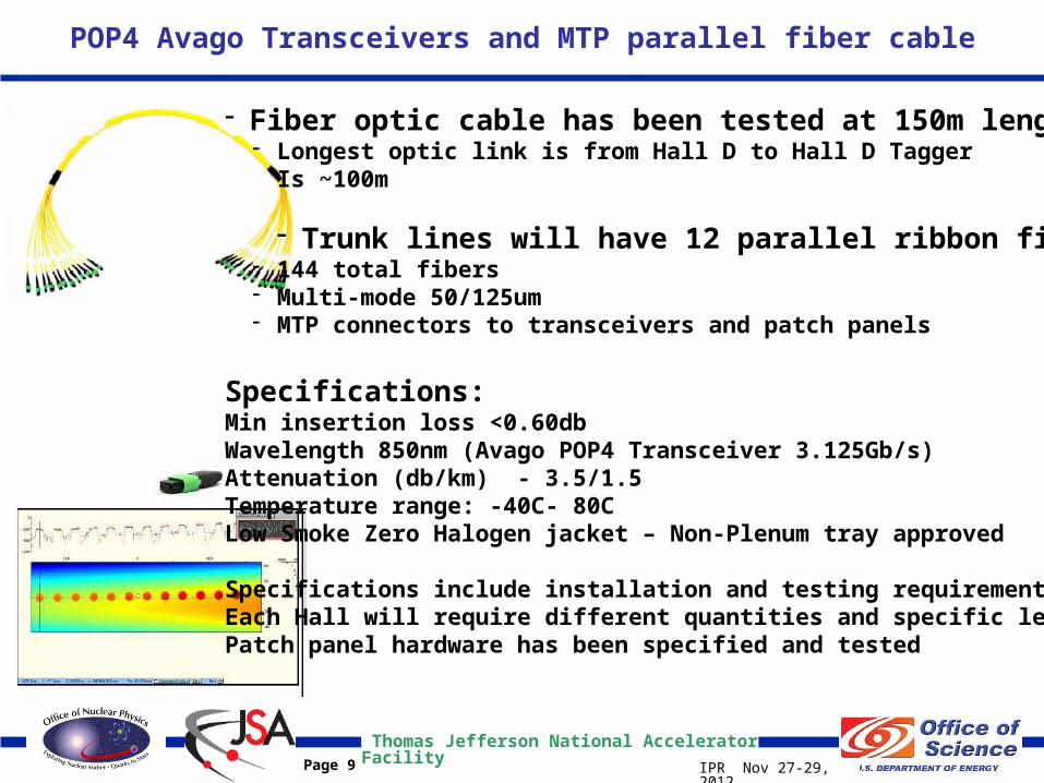
POP4 Avago Transceivers and MTP parallel fiber cable
- Fiber optic cable has been tested at 150m length- Longest optic link is from Hall D to Hall D Tagger
Is ~100m
- Trunk lines will have 12 parallel ribbon fibers- 144 total fibers- Multi-mode 50/125um- MTP connectors to transceivers and patch panels
Specifications:Min insertion loss <0.60dbWavelength 850nm (Avago POP4 Transceiver 3.125Gb/s)Attenuation (db/km) - 3.5/1.5Temperature range: -40C- 80CLow Smoke Zero Halogen jacket – Non-Plenum tray approved
Specifications include installation and testing requirementsEach Hall will require different quantities and specific lengthsPatch panel hardware has been specified and tested
Thomas Jefferson National Accelerator Facility
IPR Nov 27-29, 2012Page 10
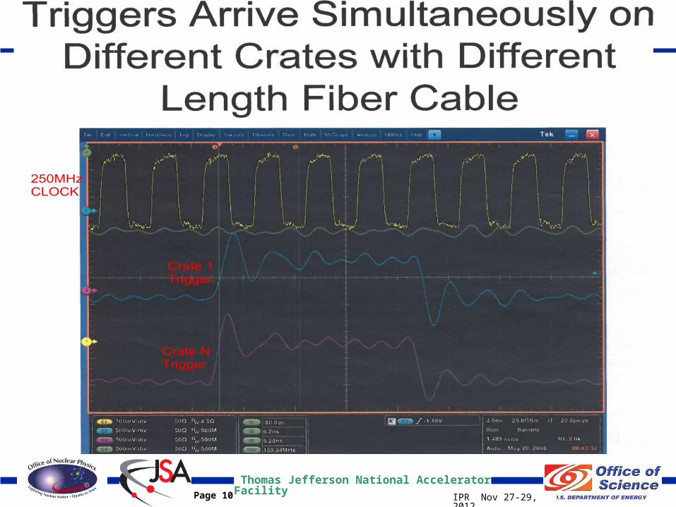
Synchronous Trigger Arrival
Thomas Jefferson National Accelerator Facility
IPR Nov 27-29, 2012Page 11
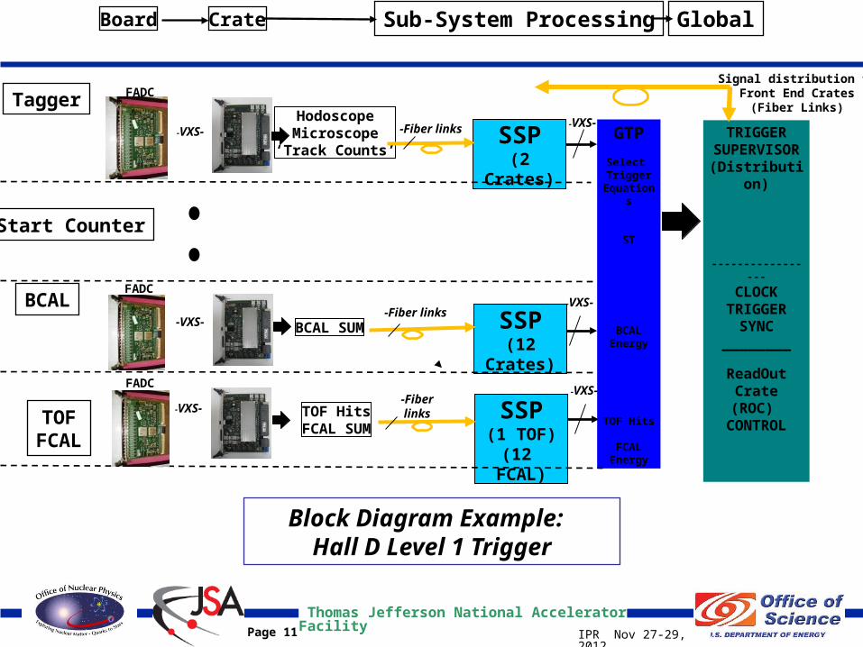
Block Diagram Example: Hall D Level 1 Trigger
HodoscopeMicroscope
‘Track Counts’SSP
(2 Crates)
FADC
FADC
FADC
-VXS-
-VXS-
-VXS- -Fiber links GTP
Select Trigger
Equations
ST
BCAL Energy
TOF Hits
FCALEnergy
TRIGGERSUPERVISOR(Distribution)
-----------------
CLOCKTRIGGER
SYNC________
ReadOutCrate
(ROC) CONTROL
Signal distribution toFront End Crates
(Fiber Links)
Board Sub-System Processing Global
Tagger
BCAL
Start Counter
BCAL SUM SSP(12 Crates)
-Fiber links
-VXS-
-VXS-
TOF HitsFCAL SUM
TOFFCAL
SSP(1 TOF)
(12 FCAL)
-VXS--Fiber links
Crate
Thomas Jefferson National Accelerator Facility
IPR Nov 27-29, 2012Page 12
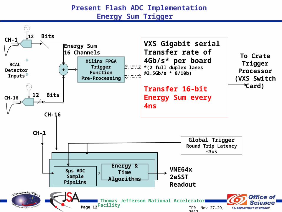
Xilinx FPGA Trigger FunctionPre-Processing
To CrateTrigger
Processor(VXS Switch Card)
BCAL Detector Inputs
Present Flash ADC ImplementationEnergy Sum Trigger
12 Bits
12 Bits
CH-1
CH-16
+
VXS Gigabit serial Transfer rate of 4Gb/s* per board*(2 full duplex lanes @2.5Gb/s * 8/10b)
Transfer 16-bit Energy Sum every 4ns
Energy Sum16 Channels
Energy & Time Algorithms
VME64x2eSST Readout
8μs ADC Sample Pipeline
Global TriggerRound Trip Latency <3us
CH-1
CH-16
Thomas Jefferson National Accelerator Facility
IPR Nov 27-29, 2012Page 13
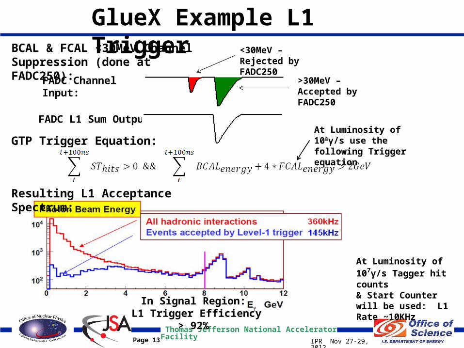
GlueX Example L1 TriggerBCAL & FCAL <30MeV Channel Suppression (done at FADC250):
FADC Channel Input:
FADC L1 Sum Output:
<30MeV – Rejected by FADC250
>30MeV – Accepted by FADC250
GTP Trigger Equation:
Resulting L1 Acceptance Spectrum:
In Signal Region: L1 Trigger Efficiency > 92%
At Luminosity of 108γ/s use the following Trigger equation
At Luminosity of 107γ/s Tagger hit counts & Start Counter will be used: L1 Rate ~10KHz
Thomas Jefferson National Accelerator Facility
IPR Nov 27-29, 2012Page 14
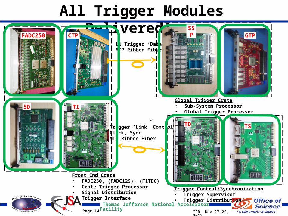
All Trigger Modules Delivered!
Front End Crate• FADC250, (FADC125), (F1TDC)• Crate Trigger Processor• Signal Distribution• Trigger Interface
Trigger Control/Synchronization• Trigger Supervisor• Trigger Distribution
FADC250 CTP
SD TI
SP
GTP
TSTD
L1 Trigger ‘Data’MTP Ribbon Fiber
Trigger ‘Link” ControlClock, SyncMTP Ribbon Fiber
Global Trigger Crate• Sub-System Processor• Global Trigger Processor
SSP
Thomas Jefferson National Accelerator Facility
IPR Nov 27-29, 2012Page 15
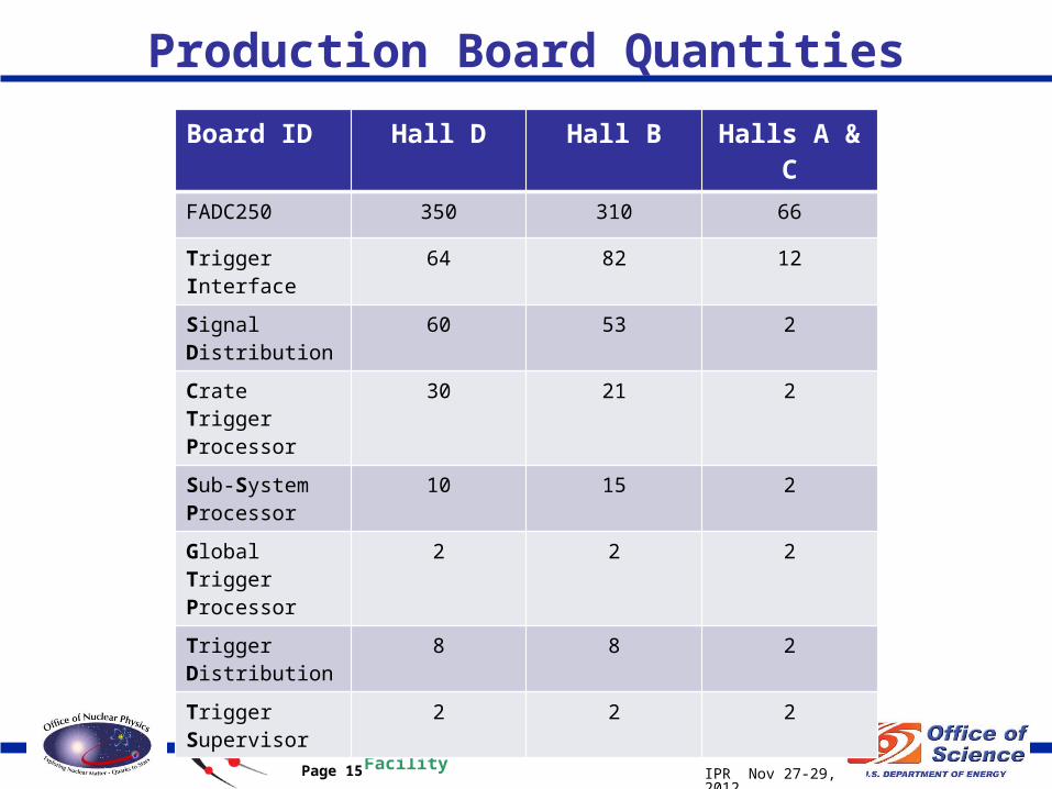
Production Board Quantities
Board ID Hall D Hall B Halls A & C
FADC250 350 310 66
Trigger Interface 64 82 12
Signal Distribution
60 53 2
Crate Trigger Processor
30 21 2
Sub-System Processor
10 15 2
Global Trigger Processor
2 2 2
Trigger Distribution
8 8 2
Trigger Supervisor
2 2 2
Thomas Jefferson National Accelerator Facility
IPR Nov 27-29, 2012Page 16
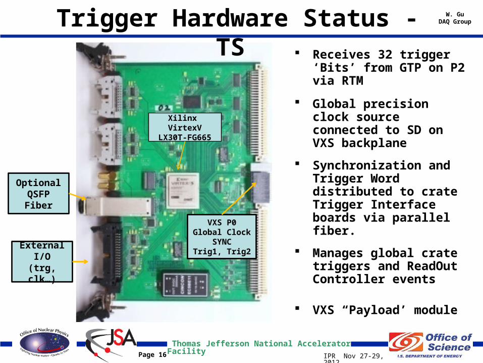
Trigger Hardware Status - TS Receives 32 trigger ‘Bits’
from GTP on P2 via RTM
Global precision clock source connected to SD on VXS backplane
Synchronization and Trigger Word distributed to crate Trigger Interface boards via parallel fiber.
Manages global crate triggers and ReadOut Controller events
VXS “Payload’ moduleExternal
I/O(trg, clk…)
Xilinx VirtexV
LX30T-FG665
W. GuDAQ Group
VXS P0Global Clock
SYNCTrig1, Trig2
Optional QSFP Fiber
Thomas Jefferson National Accelerator Facility
IPR Nov 27-29, 2012Page 17
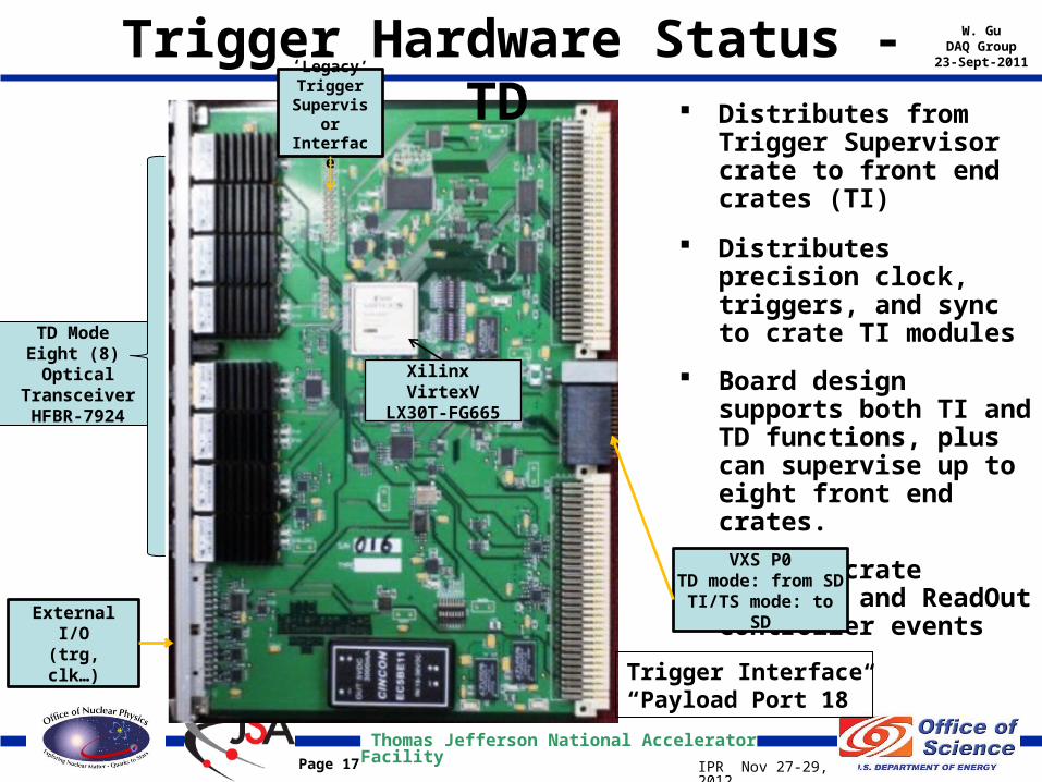
Trigger Hardware Status - TD Distributes from Trigger
Supervisor crate to front end crates (TI)
Distributes precision clock, triggers, and sync to crate TI modules
Board design supports both TI and TD functions, plus can supervise up to eight front end crates.
Manages crate triggers and ReadOut Controller events
Trigger Interface“Payload Port 18”
‘Legacy’Trigger
SupervisorInterface
External I/O(trg, clk…)
Xilinx VirtexV
LX30T-FG665
TD Mode Eight (8)
Optical TransceiverHFBR-7924
W. GuDAQ Group23-Sept-2011
VXS P0TD mode: from SDTI/TS mode: to SD
Thomas Jefferson National Accelerator Facility
IPR Nov 27-29, 2012Page 18
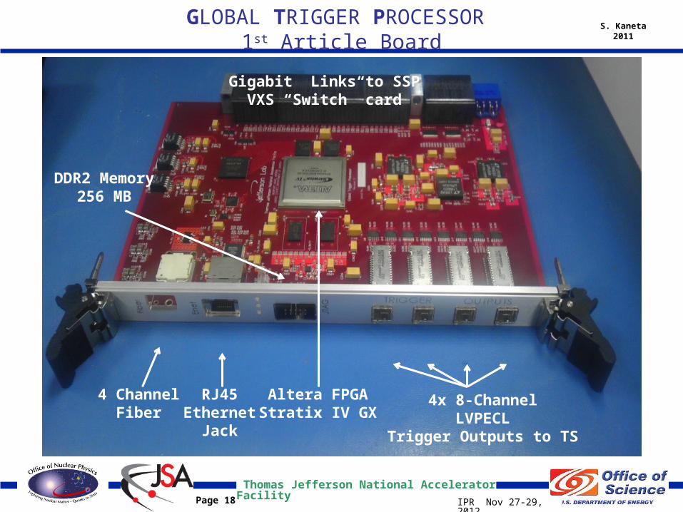
GLOBAL TRIGGER PROCESSOR 1st Article Board
4 ChannelFiber
RJ45Ethernet
Jack
4x 8-ChannelLVPECL
Trigger Outputs to TS
Altera FPGAStratix IV GX
DDR2 Memory256 MB
Gigabit Links to SSPVXS “Switch” card
S. Kaneta2011
Thomas Jefferson National Accelerator Facility
IPR Nov 27-29, 2012Page 19
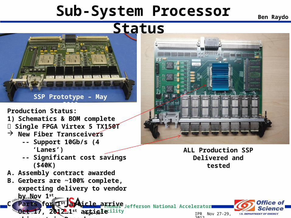
SSP Prototype – May 2010
Production Status:1) Schematics & BOM complete Single FPGA Virtex 5 TX150T New Fiber Transceivers
-- Support 10Gb/s (4 ‘Lanes’)-- Significant cost savings ($40K)
A. Assembly contract awardedB. Gerbers are ~100% complete, expecting
delivery to vendor by Nov 1st.C. Parts for 1st article arrive Oct 17, 2012…
1st article shipment in December
ALL Production SSP Delivered and tested
Sub-System Processor Status Ben Raydo
Thomas Jefferson National Accelerator Facility
IPR Nov 27-29, 2012Page 20
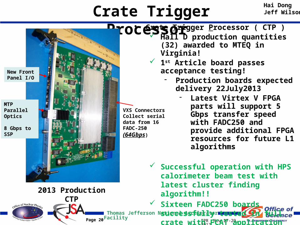
Crate Trigger Processor
VXS ConnectorsCollect serial data from 16 FADC-250(64Gbps)
Hai DongJeff Wilson
2013 Production CTP
New Front Panel I/O
• Crate Trigger Processor ( CTP ) Hall D production quantities (32)
awarded to MTEQ in Virginia! 1st Article board passes acceptance
testing!- Production boards expected
delivery 22July2013- Latest Virtex V FPGA parts
will support 5 Gbps transfer speed with FADC250 and provide additional FPGA resources for future L1 algorithms
Successful operation with HPS calorimeter beam test with latest cluster finding algorithm!!
Sixteen FADC250 boards successfully tested in full crate with FCAT application
MTP Parallel Optics
8 Gbps to SSP
Thomas Jefferson National Accelerator Facility
IPR Nov 27-29, 2012Page 21
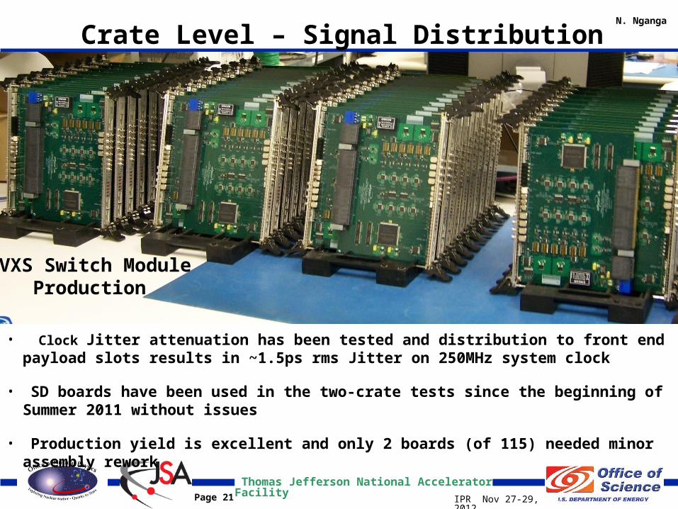
N. Nganga
Crate Level – Signal Distribution (SD)
• Clock Jitter attenuation has been tested and distribution to front end payload slots results in ~1.5ps rms Jitter on 250MHz system clock
• SD boards have been used in the two-crate tests since the beginning of Summer 2011 without issues
• Production yield is excellent and only 2 boards (of 115) needed minor assembly rework
VXS Switch ModuleProduction
Thomas Jefferson National Accelerator Facility
IPR Nov 27-29, 2012Page 22
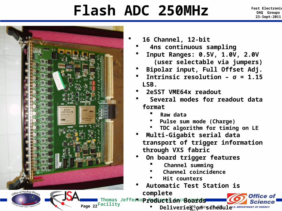
16 Channel, 12-bit 4ns continuous sampling Input Ranges: 0.5V, 1.0V, 2.0V
(user selectable via jumpers) Bipolar input, Full Offset Adj. Intrinsic resolution – σ = 1.15 LSB. 2eSST VME64x readout Several modes for readout data format
Raw data Pulse sum mode (Charge) TDC algorithm for timing on LE
Multi-Gigabit serial data transport of trigger information through VXS fabric
On board trigger features Channel summing Channel coincidence Hit counters
Automatic Test Station is complete Production Boards
Deliveries on schedule
Flash ADC 250MHz Fast ElectronicsDAQ Groups23-Sept-2011
Thomas Jefferson National Accelerator Facility
IPR Nov 27-29, 2012Page 23
CODA
MTP Fiber
MTP Fiber
LINUX
LINUX
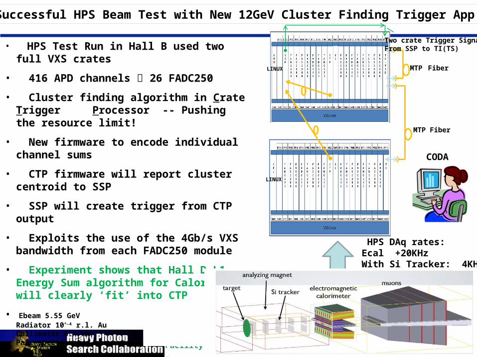
Two crate Trigger SignalFrom SSP to TI(TS)
Successful HPS Beam Test with New 12GeV Cluster Finding Trigger App
• HPS Test Run in Hall B used two full VXS crates
• 416 APD channels 26 FADC250
• Cluster finding algorithm in Crate Trigger Processor -- Pushing the resource limit!
• New firmware to encode individual channel sums
• CTP firmware will report cluster centroid to SSP
• SSP will create trigger from CTP output
• Exploits the use of the 4Gb/s VXS bandwidth from each FADC250 module
• Experiment shows that Hall D L1 Energy Sum algorithm for Calorimetry will clearly ‘fit’ into CTP
• Ebeam 5.55 GeV Radiator 10^-4 r.l. Au Collimator 6.4 mm Pair spectrometer convertor 1.8x10^-3, 4.5x10^-3 and 1.6x10^-2 r.l. Pair spectrometer field - -760A and +760A
HPS DAq rates:Ecal +20KHzWith Si Tracker: 4KHz
Thomas Jefferson National Accelerator Facility
IPR Nov 27-29, 2012Page 24
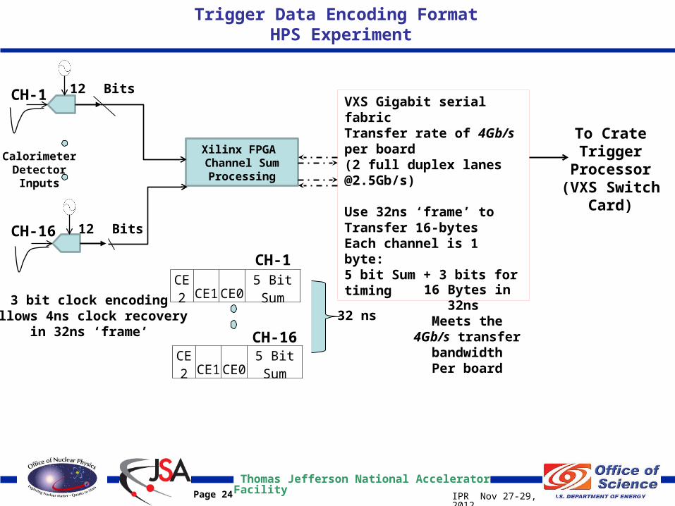
Xilinx FPGA Channel SumProcessing
To CrateTrigger
Processor(VXS Switch Card)
Trigger Data Encoding Format HPS Experiment
12 Bits
12 Bits
CH-1
CH-16
VXS Gigabit serial fabricTransfer rate of 4Gb/s per board(2 full duplex lanes @2.5Gb/s)
Use 32ns ‘frame’ to Transfer 16-bytes Each channel is 1 byte:5 bit Sum + 3 bits for timing
3 bit clock encodingAllows 4ns clock recovery
in 32ns ‘frame’
16 Bytes in 32ns Meets the 4Gb/s
transfer bandwidthPer board
CH-1
CH-16
32 ns
CE2 CE1 CE0 5 Bit Sum
CalorimeterDetector Inputs
CE2 CE1 CE0 5 Bit Sum
Thomas Jefferson National Accelerator Facility
IPR Nov 27-29, 2012Page 25
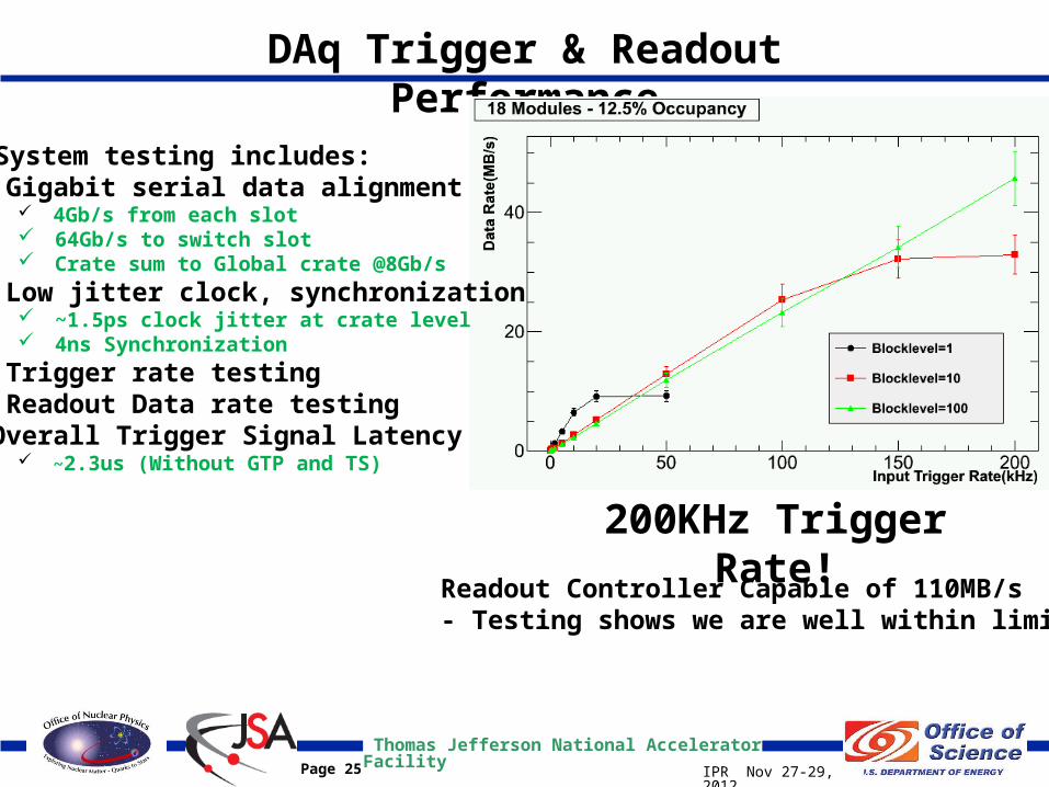
DAq Trigger & Readout Performance
200KHz Trigger Rate!
• System testing includes:• Gigabit serial data alignment
4Gb/s from each slot 64Gb/s to switch slot Crate sum to Global crate @8Gb/s
• Low jitter clock, synchronization ~1.5ps clock jitter at crate level 4ns Synchronization
• Trigger rate testing• Readout Data rate testing• Overall Trigger Signal Latency
~2.3us (Without GTP and TS)
Readout Controller Capable of 110MB/s- Testing shows we are well within limits
Thomas Jefferson National Accelerator Facility
IPR Nov 27-29, 2012Page 26
Summary FY12 production board schedules on track
• Production order for GTP and TS remain
• GTP and TS pre-production units are fully functional
- Global Crate testing has started
Parallel fiber optic transceivers/cable type has been tested
• Fiber and patch panels/cable have been ordered and received for Hall C
Two full crate DAq system used successfully for the Heavy Photon Search test in Hall B. (May 2012)• Excellent test foundation for software drivers, new calorimeter trigger
algorithms and detector commissioning tools.• Cluster finding Trigger application performance exceeds Energy
summation function required for other experiments.
Full crate hardware acceptance testing in progress • Verification of all boards in final crate configuration
Infrastructure and Engineering support/expertise exists for post CD4 Ops
Thomas Jefferson National Accelerator Facility
IPR Nov 27-29, 2012Page 27
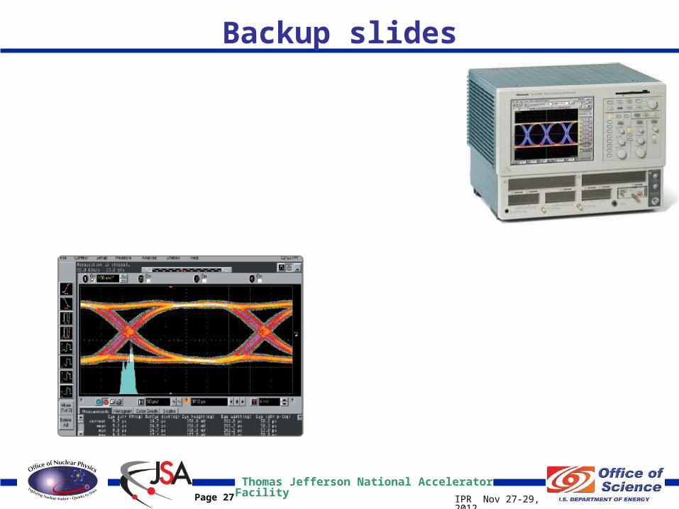
Backup slides
Thomas Jefferson National Accelerator Facility
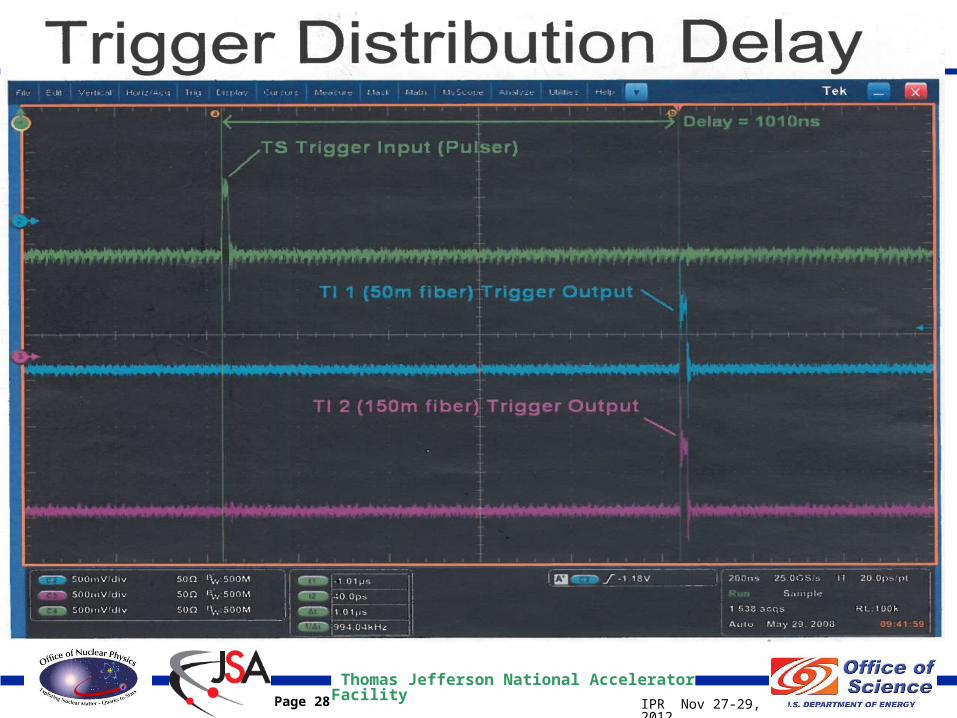
IPR Nov 27-29, 2012Page 28
Backup slides
Thomas Jefferson National Accelerator Facility
IPR Nov 27-29, 2012Page 29
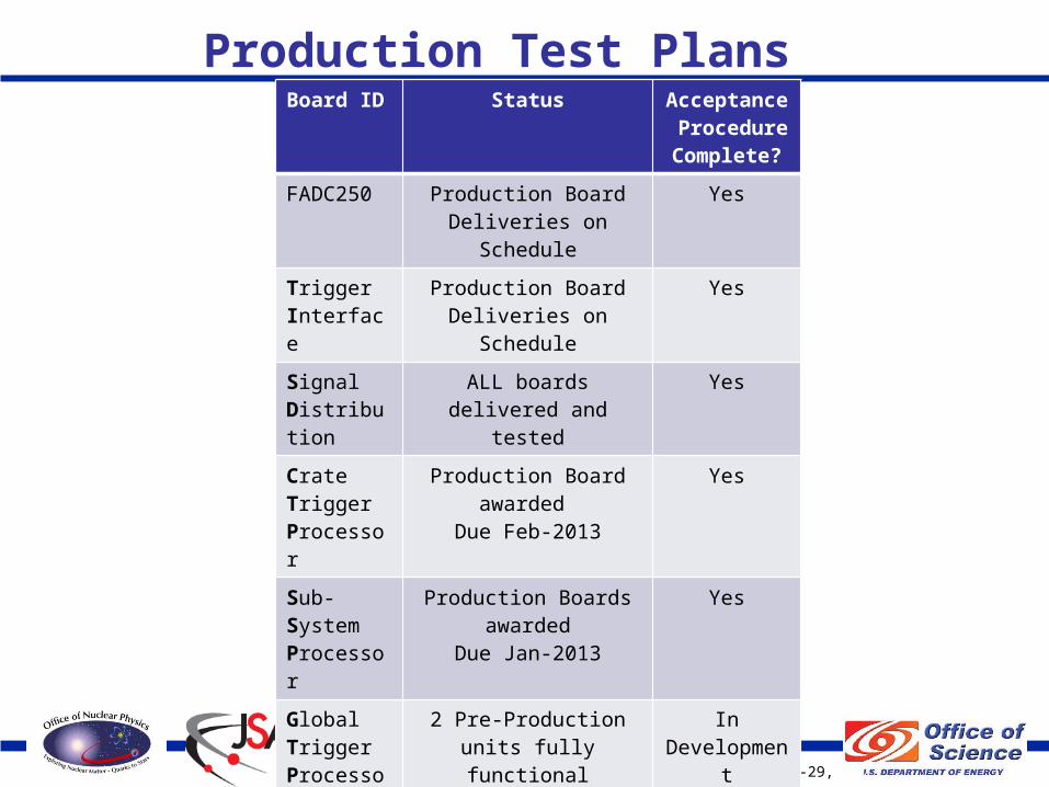
Production Test Plans Board ID Status Acceptance
Procedure Complete?
FADC250 Production Board Deliveries on Schedule
Yes
Trigger Interface
Production Board Deliveries on Schedule
Yes
Signal Distribution
ALL boards delivered and tested
Yes
Crate Trigger Processor
Production Board awarded
Due Feb-2013
Yes
Sub-System Processor
Production Boards awarded
Due Jan-2013
Yes
Global Trigger Processor
2 Pre-Production units fully functional
In Development
Trigger Distribution
Production Board Deliveries on Schedule
Yes
Trigger Supervisor
2 Pre-Production units fully functional
In Development
Thomas Jefferson National Accelerator Facility
IPR Nov 27-29, 2012Page 30
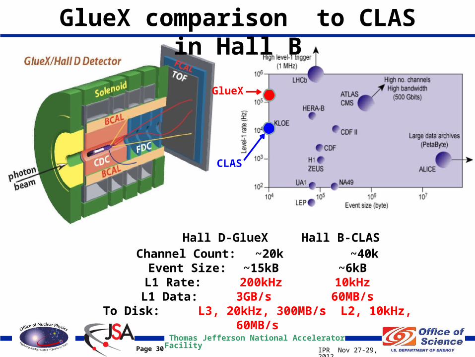
GlueX comparison to CLAS in Hall B
Hall D-GlueX Hall B-CLASChannel Count: ~20k ~40kEvent Size: ~15kB ~6kB
L1 Rate: 200kHz 10kHzL1 Data: 3GB/s 60MB/s
To Disk: L3, 20kHz, 300MB/s L2, 10kHz, 60MB/s
GlueX
CLAS
Thomas Jefferson National Accelerator Facility
IPR Nov 27-29, 2012Page 31
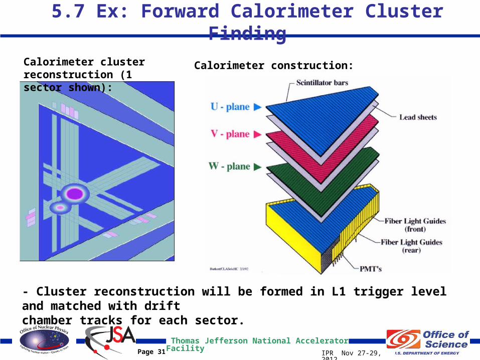
5.7 Ex: Forward Calorimeter Cluster Finding
Calorimeter clusterreconstruction (1 sector shown):
- Cluster reconstruction will be formed in L1 trigger level and matched with driftchamber tracks for each sector.
Calorimeter construction:
Thomas Jefferson National Accelerator Facility
IPR Nov 27-29, 2012Page 32
Specific to Hall D: (F. Barbosa, C. Stanislav, N. Sandoval, C. Dickover, A. Stepanyan, J. Wilson,
E. Jastrzembski(DAQ))
• F1TDC – Two versions: 32 channel high resolution; 48 channel normal resolution
• Production versions have been ordered and will be tested at UMass• FADC125 – Production boards awarded and deliveries have started• Significant production/assembly work at JLAB on the SiPM circuits for
BCAL, Start Counter and Pair Spectrometer detectors• FDC, CDC, circuit board design, inspection, testing, analysis, and
installation• Installation, schedules, coordination with collaborating institutions
Preparations for full crate DAq testing with production boards (F112) 12 full crates installed in the Hall D counting house for
CODA/DAq/Trigger testing.• Electrical safety guidance and review
More 12GeV Electronics support activities
April 19, 2023
32
Thomas Jefferson National Accelerator Facility
IPR Nov 27-29, 2012Page 33
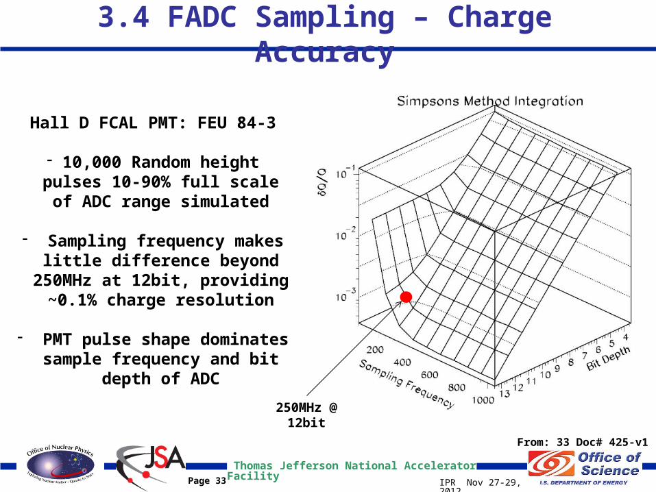
3.4 FADC Sampling – Charge Accuracy
250MHz @ 12bit
Hall D FCAL PMT: FEU 84-3
- 10,000 Random height pulses 10-90% full scale of ADC range
simulated
- Sampling frequency makes little difference beyond 250MHz at 12bit, providing ~0.1% charge resolution
- PMT pulse shape dominates sample frequency and bit depth of ADC
From: 33 Doc# 425-v1
Thomas Jefferson National Accelerator Facility
IPR Nov 27-29, 2012Page 34
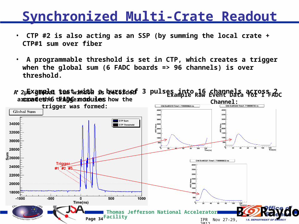
Synchronized Multi-Crate Readout• CTP #2 is also acting as an SSP (by summing the local crate + CTP#1 sum over
fiber
• A programmable threshold is set in CTP, which creates a trigger when the global sum (6 FADC boards => 96 channels) is over threshold.
• Example test with a burst of 3 pulses into 16 channels across 2 crates/6 FADC modulesA 2μs global sum window is recorded around the trigger to see how the trigger was formed:
Example Raw Event Data for 1 FADC Channel:
B. Raydo
Thomas Jefferson National Accelerator Facility
IPR Nov 27-29, 2012Page 35
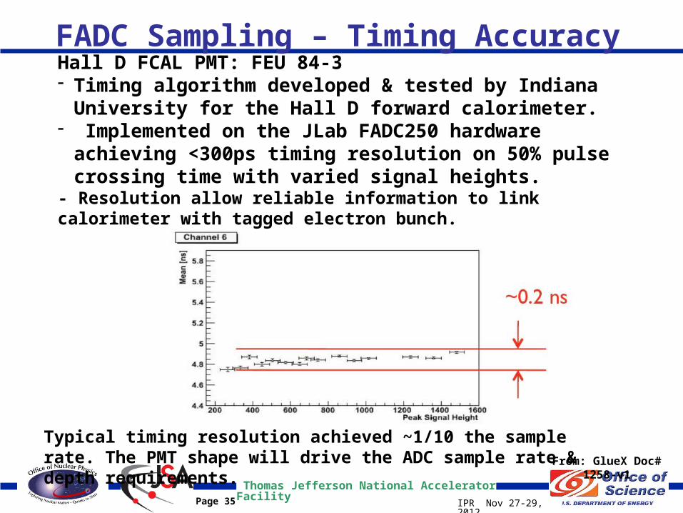
FADC Sampling – Timing Accuracy
From: GlueX Doc# 1258-v1
Hall D FCAL PMT: FEU 84-3- Timing algorithm developed & tested by Indiana University for the
Hall D forward calorimeter.- Implemented on the JLab FADC250 hardware achieving <300ps
timing resolution on 50% pulse crossing time with varied signal heights.
- Resolution allow reliable information to link calorimeter with tagged electron bunch.
Typical timing resolution achieved ~1/10 the sample rate. The PMT shape will drive the ADC sample rate & depth requirements.
Thomas Jefferson National Accelerator Facility
IPR Nov 27-29, 2012Page 36
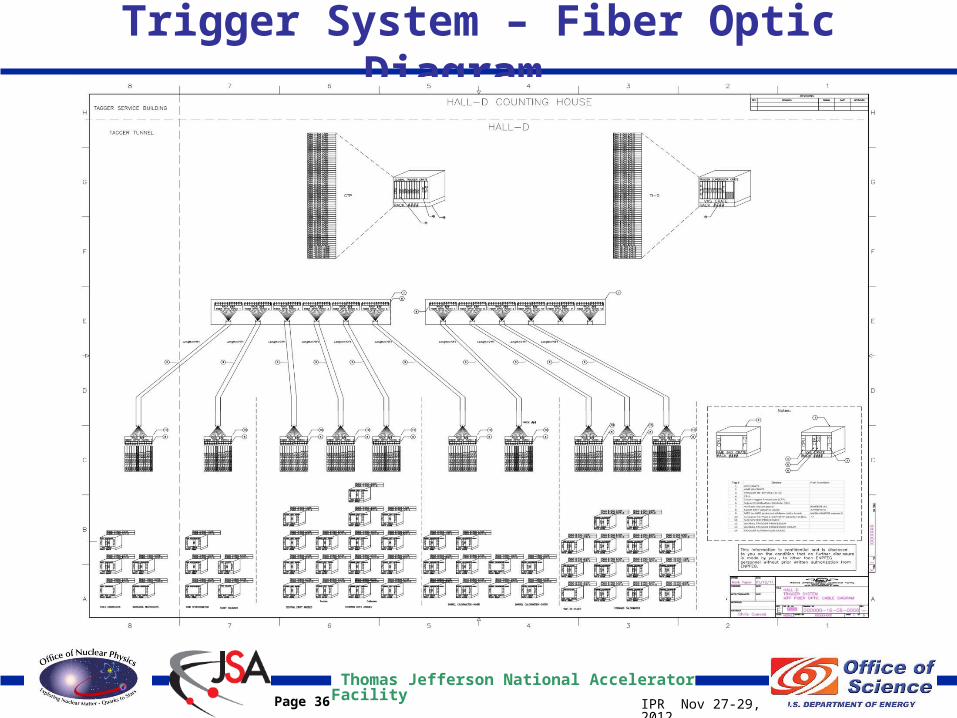
Trigger System – Fiber Optic Diagram
Thomas Jefferson National Accelerator Facility
IPR Nov 27-29, 2012Page 37
CLAS12 Data Acquisition System• 3724 channels of 12bit 250MHz Flash ADCs • 3724 channels of 85ps and 35ps resolution pipeline TDCs with
discriminators collecting data from:– 2 Calorimeters per sector – PCAL, ECAL– 2 Cerenkov counters – HTCC, CC/sector– Time-of-flight detectors – CTOF, TOF/sector
• All electronics is compatible with pipelined DAQ concept• 24192 channels from Drift Chambers (TDC w/1ns LSB)
– Drift Chamber Readout Board with Tracking Trigger Features• Central tracker readout system• >50 VME/VME64X/VXS crates equipped with Readout Controllers and
Trigger Interface Units• JLAB Trigger System Modules
– Benefit from Hall D 200KHz Trigger rate design requirement• JLAB CODA DAQ software