Embed Size (px)
Citation preview

T h e o p e n – a c c e s s j o u r n a l f o r p h y s i c s
New Journal of Physics
Spatially highly resolved study of AFM scanningtip–quantum dot local interaction
S Kicin1, A Pioda1, T Ihn1, M Sigrist1, A Fuhrer1, K Ensslin1,M Reinwald2 and W Wegscheider2
1 Solid State Physics, ETH Zürich, 8093 Zürich, Switzerland2 Institut für experimentelle und angewandte Physik, Universität Regensburg,GermanyE-mail: [email protected]
New Journal of Physics 7 (2005) 185Received 19 April 2005Published 26 August 2005Online at http://www.njp.org/doi:10.1088/1367-2630/7/1/185
Abstract. Scanning-gate imaging of semiconductor quantum dots (QDs)promises access to probability distributions of quantum states. It could thereforebe a novel tool for designing and optimizing tailored quantum states in suchsystems. A detailed study of a lithographically defined semiconductor QD inthe Coulomb-blockade regime is presented, making use of the scanning-gatetechnique at a base temperature of 300 mK. The method allows a one-by-onemanipulation of electrons in the structure. The obtained images interpreted witha suitable QD model guide the way to a local investigation of the electronicinterior of the QD. Future perspectives of scanning-gate experiments on QDs arediscussed.
New Journal of Physics 7 (2005) 185 PII: S1367-2630(05)98563-71367-2630/05/010185+18$30.00 © IOP Publishing Ltd and Deutsche Physikalische Gesellschaft

2 Institute of Physics �DEUTSCHE PHYSIKALISCHE GESELLSCHAFT
Contents
1. Introduction 22. Sample, setup and description of the experiment 3
2.1. Sample fabrication and characterization . . . . . . . . . . . . . . . . . . . . . 32.2. Preparation and description of the scanning-gate experiment . . . . . . . . . . 3
3. Scanning-gate measurements 63.1. Tip-voltage dependence . . . . . . . . . . . . . . . . . . . . . . . . . . . . . . 63.2. Model for the tip–dot interaction . . . . . . . . . . . . . . . . . . . . . . . . . 63.3. Discussion of the data in the light of the model . . . . . . . . . . . . . . . . . 83.4. Scanning-gate measurements in the QD interior . . . . . . . . . . . . . . . . . 113.5. Discussion in terms of the model . . . . . . . . . . . . . . . . . . . . . . . . . 11
4. Effects of the tip on lever arms and charging energy 155. What are the conditions for true wave function mapping? 166. Conclusions 16Acknowledgments 17References 17
1. Introduction
The physical realization of quantum communication and quantum computing requires veryprecise control over the quantum states used to represent the elementary carrier of information,the qubit, and over the phase-coherent interaction between qubits [1, 2]. In the last 15 years,experimental physicists have made enormous progress in quantum dot (QD) fabrication and theyhave achieved impressive control over the dot’s electronic charge [3, 4] and the properties of itsindividual orbital [5] and spin states [6]–[9]. As a consequence, proposals have been developedto utilize either orbital- or spin-degrees of freedom in QDs as the physical implementation of aqubit [10, 11]. Since then, QD design has been readily improved for achieving laterally definedQDs with one or two electrons [12] which exhibit the physics of (QD) hydrogen with only asingle occupied state [12]–[14], or helium with its singlet ground state and its triplet excited state[12, 13, 15].
Parallel to these developments, scanning probe microscopy (SPM) techniques have beenapplied for the investigation of semiconductor nanostructures. Spatially resolved single-chargedetection has, for example, been achieved using a scanning metallic single-electron transistor[16, 17]. Scanning experiments with only a sharp metallic tip coupled capacitively to a two-dimensional electron gas (2DEG) subject to a high magnetic field were interpreted in terms of theformation of a few-electron bubble forming underneath the tip [18]. SPM was also used to imagecoherent electron flow in the vicinity of a quantum point contact [19]. Similar experiments onquantum point contacts and quantum billiards were interpreted as showing the spatially resolvedprobability density distribution of quantum states [20].
Scanning-probe techniques can also be applied to QDs with the aim of extracting informationabout quantum states beyond that obtainable by transport experiments alone. These techniquespotentially offer spatially resolved access to the properties of QDs. The enormous variety ofmethods that have been developed or are within reach, promise unforeseen further potential
New Journal of Physics 7 (2005) 185 (http://www.njp.org/)

3 Institute of Physics �DEUTSCHE PHYSIKALISCHE GESELLSCHAFT
for improving qubit design, preparation, interaction and measurement. Pioneering scanningexperiments on QDs were reported by McEuen et al using dots forming at imperfections incarbon nanotubes [21]. They employed the so-called scanning-gate technique, in which a sharpscanning metallic tip couples capacitively to the QD under investigation. A lithographicallyfabricated semiconductor QD was recently studied with the same technique in [22, 23]. This typeof experiment was theoretically investigated in [24]. Despite the experimental achievements,no experiment has so far presented convincing evidence for mapping QD wave functions orprobability densities in real space and this issue remains one of the most challenging and importantmilestones for the extensive use of SPM for even more sophisticated experiments on single andcoupled QD qubits.
In this paper, we present a detailed study of a lithographically defined semiconductor QDin the Coulomb blockade (CB) regime using the scanning-gate technique at a temperature of300 mK. Compared with previous experiments, conductance resonances could be observed withthe tip scanning at a constant height above the interior of the QD. The experimental results arediscussed in terms of a QD model that captures the essential physics of the measurement. Thetip–dot interaction potential was reconstructed from experimental data. Future perspectives ofutilizing the scanning-gate technique for the investigation of QDs are discussed.
2. Sample, setup and description of the experiment
2.1. Sample fabrication and characterization
The QD under investigation was realized on a GaAs/AlGaAs heterostructure grown by molecularbeam epitaxy containing a 2DEG with electron density of 5 × 1011 cm−2 and 34 nm belowthe surface. The electron mobility was determined to be 450 000 cm2 V s−1 at a temperatureof 4.2 K. In the first processing step, a 25 × 25 µm2 mesa was defined by optical lithographyand subsequent wet chemical etching. In the second step, many nanostructures were defined onthe surface of the mesa by local anodic oxidation along certain lines using a room temperaturescanning force microscope (SFM) [25]–[27]. The 2DEG is depleted below the oxide lines suchthat mutually isolated structures were realized (see figure 1(a)). Among them was the QD ofinterest here with a topographic size of 350 × 400 nm2. The three quantum point contacts in thevicinity of the dot will not be further discussed in this paper.
Gates labelled ‘G1’ and ‘G2’ were used to tune the QD’s coupling to source and drainreservoirs. The lateral plunger gate (PG) allowed to control the number of electrons in the dot.Figure 1(b) shows a measurement of the dot conductance as a function of the voltage UPG on thePG. This measurement was taken at a temperature of 300 mK operating the QD in the CB regime.The average charging energy of the QD was determined from CB diamonds to be ∼0.8 meV.The average separation of single-particle energies estimated from the geometry of the QD is∼30 µeV assuming a depletion length of 100 nm. The conductance resonances in figure 1(b) arethermally broadened with an electron temperature of 550 mK. Since the average single-particlelevel spacing is smaller than the thermal broadening of conductance resonances, we operate thedot in a few-level transport regime.
2.2. Preparation and description of the scanning-gate experiment
Scanning-gate measurements were performed using a home-built low temperature SFM operatedin a He3 cryostat with a base temperature of 300 mK [28]. A piezoelectric tuning fork sensor with
New Journal of Physics 7 (2005) 185 (http://www.njp.org/)

4 Institute of Physics �DEUTSCHE PHYSIKALISCHE GESELLSCHAFT
-150 -100 -50
0.00
0.01
0.02
0.03
0.04
0.05
PG voltage (mV)
Dot
con
duct
ance
(e2
/h)
G1
G2
PG
ISD
QD
a.1(b)
(a)
930 nm
Figure 1. (a) Topography of the structure obtained by SFM at room temperature.Note that the microscope and tip used for acquiring this image differ from thecryogenic SFM equipment employed for the measurements presented in thefollowing figures. (b) Conductance resonances measured by sweeping UPG withUSD = 20 µV symmetrically applied.
an electrochemically sharpened PtIr tip which could be electrostatically biased, was employedas the scanning probe [28].
Experiments similar to those presented below were performed before on another sampleand on the sample presented here. Although scanning-gate images had been obtained in the CBregime, a direct study of the dot interior had not been possible due to a strong conductanceincrease when the negatively biased tip was positioned above the dot [22].
It turned out that in the experiments presented here, this conductance increase was notobserved. Our present experience suggests that this may be due to the fact that, in contrast toprevious cooldowns, we performed only scans at constant height above the surface (typically60–150 nm) at base temperature. Before these scans, the QD was positioned in the centre of thescan range using the built-in coarse positioning x–y-motor and a series of topography scans onthe surface with zero applied tip-voltage at an elevated temperature of 35 K. The aim of thisprocedure was to avoid any charging of the surface or charge rearrangements in the doping planeabove the structure. The tip position with respect to the dot and the sharpness of the tip wereagain verified at the end of all experiments.
While the tip was scanned, the source–drain current ISD was recorded. To this end, alow-frequency source–drain voltage USD = 20 µV was applied symmetrically (i.e., +10 µVapplied to the source contact and −10 µV to the drain). The resulting ac ISD was measuredwith a lock-in. Scanning-gate images, such as those presented in figure 2, are colour coded mapsof the linear response dot conductance G = ISD/USD = dISD/dUSD in the two-dimensional plane
New Journal of Physics 7 (2005) 185 (http://www.njp.org/)

5 Institute of Physics �DEUTSCHE PHYSIKALISCHE GESELLSCHAFT
0.05
0.04
0.03
0.02
0.01
0
Conductance (e
2/h)
0.015
0.010
0.005
0
Conductance (e
2/h)
0.008
0.006
0.004
0.002
0
Conductance (e
2/h)
0.006
0.005
0.004
0.003
0.002
0.001
0
0.01
0.008
0.006
0.004
0.002
0
0.025
0.02
0.015
0.01
0.005
0
400nm
(1)
(2)
(a) (b)
(c)
(e) (f)
(d)
Figure 2. Scanning-gate images (2500 × 2000 nm2) obtained by varying Utip.Tip-voltages are (a) Utip = 0 mV, (b) 30 mV, (c) 60 mV, (d) 120 mV, (e) 150 mVand (f) 510 mV.
of the tip position. The maximum resolution of the images was 88 000 pixel µm2 correspondingto a pixel separation of 3.37 nm.
Excellent reproducibility of the scans was found by repeating scans or by coming backto previous parameters after several other scans. During the experiment reported here, morethan 300 scans were taken. During this time three significant changes of the QD state occurredmaking it necessary to readjust the gate voltages. At least two of these events correspondedto the appearance of a particle on the surface in the vicinity of the dot. These particles weredetected in images of the tuning fork sensor frequency shift during constant height scans andverified by surface scanning at the end of the experiment. Each series of scanning-gate imagespresented below was recorded with the dot remaining in one of its stable states and during asingle condensation cycle of the 3He system.
New Journal of Physics 7 (2005) 185 (http://www.njp.org/)

6 Institute of Physics �DEUTSCHE PHYSIKALISCHE GESELLSCHAFT
3. Scanning-gate measurements
3.1. Tip-voltage dependence
Figure 2 shows scanning-gate images selected from a series taken at different tip-voltagesbetween Utip = 0 (figure 2(a)) and 540 mV in steps of 15 mV. The tip was scanned at a distance of150 nm from the surface. The images in figures 2(a)–(c) show a set of ring-shaped conductanceresonances called ‘set B’ (‘B’ stands for ‘bottom’) around the location of the QD. Between theresonances, the current is blocked and the number of electrons in the dot is fixed to an integervalue. Crossing a conductance resonance corresponds to changing the electron number in thedot by one.
The conductance rings show deformations of their shape, e.g., the one marked (1) infigure 2(a). In figure 2(d), a new conductance resonance spot marked (2) appears in the samelocation. For further increasing tip-voltages (figures 2(d)–(f)) another set of rings appears (‘set T’,where ‘T’stands for ‘top’) around the position of the spot. The separation of the centres of the twosets ‘B’ and ‘T’ is more than 600 nm.
Closer inspection of ‘set B’ in figures 2(a)–(e) shows that the diameter of conductanceresonance rings decreases continuously as a result of the increasing voltage. The image shownin figure 2(f) taken with Utip = 510 mV shows the situation where ‘set T’ dominates and‘set B’ consists of only two fringes. For even higher tip-voltage (not shown), ‘set B’ completelydisappears. In contrast to ‘set B’, the rings in ‘set T’ increase their diameter with increasing tip-voltage. In the following, we will show that the appearance of these two sets of fringes indicatethe existence of a double-tip shape.
3.2. Model for the tip–dot interaction
We present a pragmatic model for the influence of the tip on the dot which is essentially basedon the constant interaction model for QDs [29] taking the tip as an additional gate electrodewith variable position into account. Although our experiments have not been performed in thesingle-level transport regime, we neglect transport through several levels in order to achievea transparent and compact notation which still represents the underlying physics. With thesesimplifications, the energy required for adding an electron to the QD containing already n − 1excess electrons, i.e., the electrochemical potential µn, can be written as
µn = µn(�r; Utip) = εn(�r; Utip) − e∑
i
αi(�r)�Ui + ne2
C�(�r), (1)
where �r is the position of the tip. The last term on the right-hand side is the familiar chargingenergy term with the self-capacitance C� leading—in the absence of the other two terms—to aladder of equally spaced ‘energy levels’ in the dot for the number n of electrons running througha sequence of integer numbers. In the language of the Hartree approximation, e2/C� correspondsto the average Hartree energy per electron. The second term describes the influence of voltagechanges �Ui on gate i which allow to shift the ladder of energy levels up or down accordingto the gate-dependent lever arm αi. Within the Hartree approximation, each lever arm is theexpectation value of the characteristic electrostatic function of the corresponding gate electrodeevaluated with the relevant single-particle wave function in the QD. The last two terms takentogether describe the contribution of the electrostatic potential to the electrochemical potential.
New Journal of Physics 7 (2005) 185 (http://www.njp.org/)

7 Institute of Physics �DEUTSCHE PHYSIKALISCHE GESELLSCHAFT
The first term in equation (1) is the contribution of the quantization of quantum states due to theconfinement which can be seen as a single-particle energy level for the electron to be added inthe bare confinement potential, or as the chemical potential for adding electron number n.
The action of the tip on the QD enters in equation (1) in several places. Firstly, the tip is one ofthe gate electrodes i that have a certain lever arm on the QD. It is obvious that the lever arm of thetip, αtip, will depend on the position of the tip relative to the dot. If the tip–dot separation becomesmuch larger than the separation of other gates from the dot, αtip will be very small compared toall other lever arms. Because all the αi sum up to one due to fundamental arguments, the tip-position-dependence of αtip will in general also imply the tip-position-dependence of all otherlever arms. This effect can be interpreted as a result of screening, i.e., the metallic tip screens theelectric field lines originating from a specific gate and ending on the QD. While the screeningeffect itself is (in our pragmatic approximation) independent of the voltages applied to gatesand tip, the total second term in equation (1) depends linearly on the tip-voltage. This lineardependence can be seen as a result of a Taylor series expansion for small voltage changes aroundan operating point.
The second place where the presence of the tip enters equation (1) is the self-capacitance C�
of the QD. This quantity is the sum of all capacitance coefficients between gates and QD. Whenthe position of the tip relative to the dot is changed, the mutual capacitance between the two isalso changed implying a change in C�. This effect can also be seen as the screening influence ofthe tip, because its presence allows to screen an additional charge on the dot in a spatial region,where no screening would occur in the absence of the tip. This screening effect is in our modelindependent of the tip-voltage (again, assuming small tip-voltage changes).
The third way how the tip enters equation (1) is by changing the single-particle wave functionof the electron to be added and thereby the single-particle energy εn. For a weak tip-inducedpotential in the dot this effect may be treated by perturbation theory.
At this point, it is due to define what we call the interaction potential between the tip and theQD. When the tip is far away from the dot, its influence on the electrochemical potentials will benegligible and they will take on constant values µ(0)
n independent of the exact tip position. In thefollowing, we will call the tip-induced change �µn(�r) = µn(�r) − µ(0)
n the ‘interaction potentialbetween tip and dot’.
With this model of the electrochemical potential for adding an electron to the QD, we canexpress the (linear response) conductance through the dot in the weak-coupling regime as
G(�r) =∑
n
Gmax(�r)cosh2{[µn(�r) − µSD]/2kT } , (2)
with
Gmax(�r) = e2
4kTh
�(n)L (�r)�(n)
R (�r)�
(n)L (�r) + �
(n)R (�r) .
Here µSD is the electrochemical potential in the source and drain contacts, T is the electrontemperature and �
(n)L and �
(n)R are the tunnel coupling constants of the nth level to the left (source)
and right (drain) leads, respectively. The conductance shows thermally broadened resonanceswhenever one of the µn is equal to µSD. The conductance is exponentially suppressed, if µn
differs by more than 2 kT from resonance, implying that co-tunnelling is neglected in our model.In addition to the influence of the tip on µn discussed above, the tip also acts directly on the tunnel
New Journal of Physics 7 (2005) 185 (http://www.njp.org/)
8 Institute of Physics �DEUTSCHE PHYSIKALISCHE GESELLSCHAFT
coupling constants �(n)L and �
(n)R making Gmax tip-position-dependent as well. This modulates
the amplitude of conductance resonances as a function of tip position.
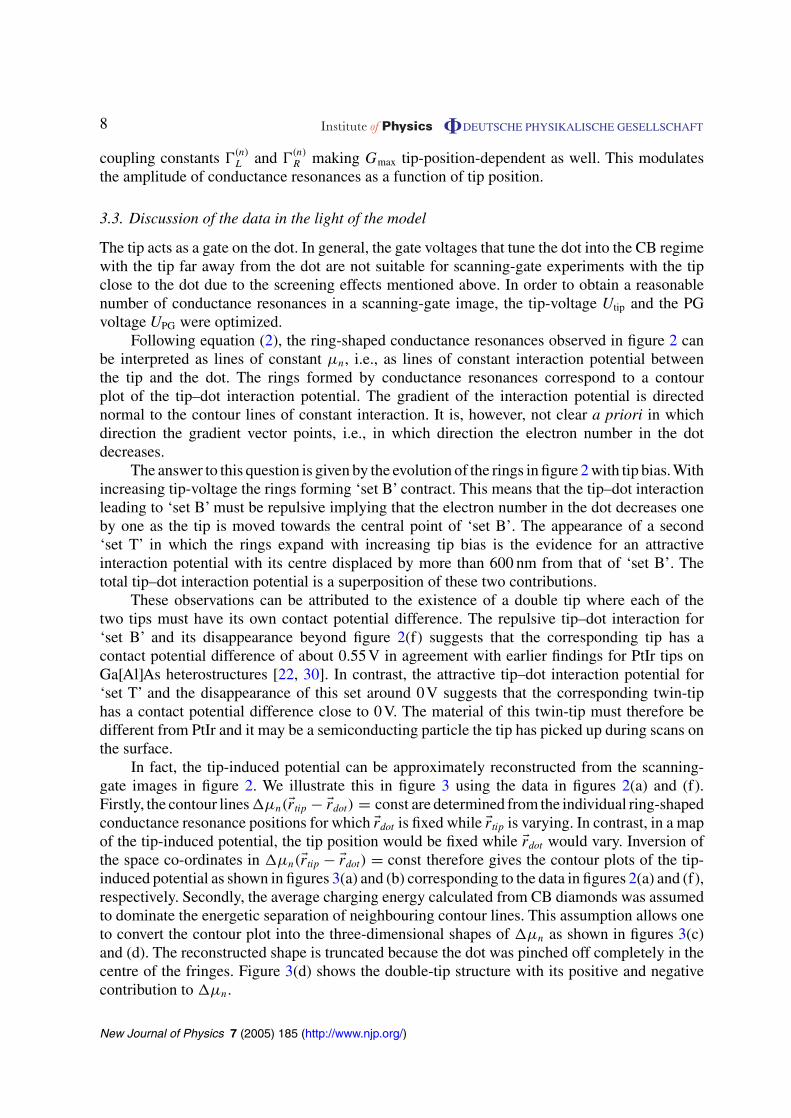
3.3. Discussion of the data in the light of the model
The tip acts as a gate on the dot. In general, the gate voltages that tune the dot into the CB regimewith the tip far away from the dot are not suitable for scanning-gate experiments with the tipclose to the dot due to the screening effects mentioned above. In order to obtain a reasonablenumber of conductance resonances in a scanning-gate image, the tip-voltage Utip and the PGvoltage UPG were optimized.
Following equation (2), the ring-shaped conductance resonances observed in figure 2 canbe interpreted as lines of constant µn, i.e., as lines of constant interaction potential betweenthe tip and the dot. The rings formed by conductance resonances correspond to a contourplot of the tip–dot interaction potential. The gradient of the interaction potential is directednormal to the contour lines of constant interaction. It is, however, not clear a priori in whichdirection the gradient vector points, i.e., in which direction the electron number in the dotdecreases.
The answer to this question is given by the evolution of the rings in figure 2 with tip bias. Withincreasing tip-voltage the rings forming ‘set B’ contract. This means that the tip–dot interactionleading to ‘set B’ must be repulsive implying that the electron number in the dot decreases oneby one as the tip is moved towards the central point of ‘set B’. The appearance of a second‘set T’ in which the rings expand with increasing tip bias is the evidence for an attractiveinteraction potential with its centre displaced by more than 600 nm from that of ‘set B’. Thetotal tip–dot interaction potential is a superposition of these two contributions.
These observations can be attributed to the existence of a double tip where each of thetwo tips must have its own contact potential difference. The repulsive tip–dot interaction for‘set B’ and its disappearance beyond figure 2(f) suggests that the corresponding tip has acontact potential difference of about 0.55V in agreement with earlier findings for PtIr tips onGa[Al]As heterostructures [22, 30]. In contrast, the attractive tip–dot interaction potential for‘set T’ and the disappearance of this set around 0V suggests that the corresponding twin-tiphas a contact potential difference close to 0V. The material of this twin-tip must therefore bedifferent from PtIr and it may be a semiconducting particle the tip has picked up during scans onthe surface.
In fact, the tip-induced potential can be approximately reconstructed from the scanning-gate images in figure 2. We illustrate this in figure 3 using the data in figures 2(a) and (f).Firstly, the contour lines �µn(�rtip − �rdot) = const are determined from the individual ring-shapedconductance resonance positions for which �rdot is fixed while �rtip is varying. In contrast, in a mapof the tip-induced potential, the tip position would be fixed while �rdot would vary. Inversion ofthe space co-ordinates in �µn(�rtip − �rdot) = const therefore gives the contour plots of the tip-induced potential as shown in figures 3(a) and (b) corresponding to the data in figures 2(a) and (f),respectively. Secondly, the average charging energy calculated from CB diamonds was assumedto dominate the energetic separation of neighbouring contour lines. This assumption allows oneto convert the contour plot into the three-dimensional shapes of �µn as shown in figures 3(c)and (d). The reconstructed shape is truncated because the dot was pinched off completely in thecentre of the fringes. Figure 3(d) shows the double-tip structure with its positive and negativecontribution to �µn.
New Journal of Physics 7 (2005) 185 (http://www.njp.org/)

9 Institute of Physics �DEUTSCHE PHYSIKALISCHE GESELLSCHAFT
Figure 3. Reconstruction of the tip–dot interaction potential �µn obtained fromscanning-gate images for two different Utip. Pictures (a) and (b) show contourlines representing constant tip–dot interaction potential (lines along currentresonances). They were obtained from figure 2(a) (Utip = 0 mV) and figure 2(f)(Utip = 510 mV). The energetic separation of the contour lines is taken to bethe average charging energy of the dot. (c) Three-dimensional image of �µn
reconstructed from (a) for Utip = 0 mV. The interaction potential is repulsive.(d) Three-dimensional image of �µn reconstructed for Utip = 510 mV. Theinteraction potential is mainly attractive.
The finding that the two tips were more than 600 nm displaced from each other, the verydifferent contact potential differences of the two and the fact that both offered a comparableresolution in scanning-gate images allowed us to use each of them separately for furtherinvestigations of the QD, if the scan range was kept well below their separation. Suchmeasurements will be described in section 3.4.
We continue with a discussion of the width and separation of conductance peaks in thescanning-gate images of figure 2. It can be seen, e.g., in figure 2(a) that the outer ring-shapedconductance resonances appear to be broader than the inner ones. At the same time, the spacingbetween the outer resonances is significantly larger than that of the inner ones. Both effects aremanifestations of the exact spatial shape of the tip–dot interaction potential. Energy differences�E, like the energetic spacing of conductance peaks, or the width of conductance peaks
New Journal of Physics 7 (2005) 185 (http://www.njp.org/)

10 Institute of Physics �DEUTSCHE PHYSIKALISCHE GESELLSCHAFT
A
B
C
∆x
∆x
∆x
∆E
∆Ε
∆Ε
X position
Tip
indu
ced
pote
ntia
l
Figure 4. Schematic drawing illustrating the influence of a repulsive tip–dotinteraction on the width and spacing of tip-induced conductance resonances. Thetip-induced change of µn is sketched in one dimension as a Lorentzian curve.�E represents the thermal broadening/spacing of conductance peaks. �x is thedistance necessary to go either through one Coulomb peak or from one Coulombpeak to the next one.
(about 3.5 kT for thermal broadening) are, to lowest order, translated into spatial separations|��r| by
|��r| = �E
|∇µn(�r)| . (3)
If the spatial gradient of the tip–dot interaction |∇µn(�r)| is small, conductance peaks are farapart in space and their spatial width is large as well. The opposite is true for large |∇µn(�r)|.Figure 4 illustrates this situation in one dimension with a Lorentzian-shaped model curve forµn(x). Large spacings and widths of conductance peaks are expected for large lateral tip–dotseparations (A) and for the case that the tip sits directly above the dot (C). The latter situation inwhich |∇µn(�r)| can become zero will be further discussed in section 3.4. Small separations andwidths of conductance resonances are observed in the intermediate regime of tip–dot separation(B), where the slope of |∇µn(�r)| is largest. The typical gradient of the tip–dot interaction potentialobserved in our experiments is |∇µn(�r)| = 2–4 µeV nm−1.
We conclude the analysis of the scans in figure 2 with a discussion about the dependenceof the conductance peak amplitude Gmax on tip position. In figures 2(a)–(e), it becomes evidentthat the amplitude for each of the conductance fringes in ‘set B’is enhanced with the tip to the rightof the fringe centre, while it is strongly suppressed with the tip to the left. The conductance peakamplitude Gmax obtained from conductance fringes of ‘set T’ in figure 2(f) shows the oppositebehaviour, i.e., peaks are enhanced to the left of the centre of the fringes and weaker to the right.For both sets, the action of the tip is much stronger on the left of the QD (i.e., the respectivefringe centre) indicating that the coupling to the left lead dominates Gmax. This behaviour ofthe two sets of fringes is another manifestation of the double-tip with a repulsive tip and anattractive twin.
New Journal of Physics 7 (2005) 185 (http://www.njp.org/)
11 Institute of Physics �DEUTSCHE PHYSIKALISCHE GESELLSCHAFT
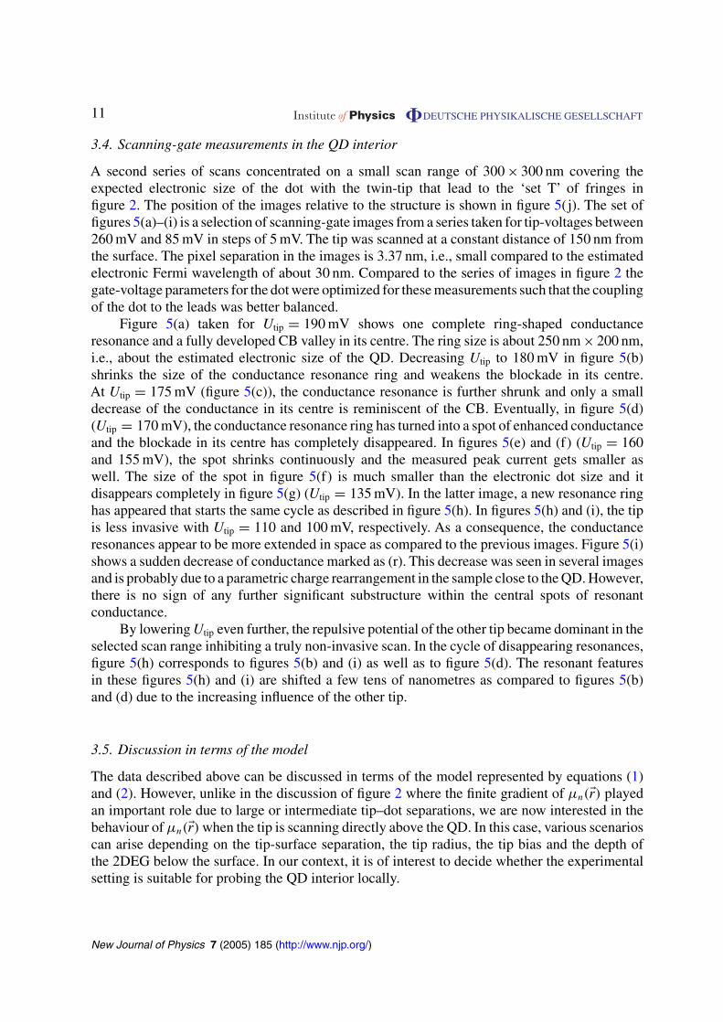
3.4. Scanning-gate measurements in the QD interior
A second series of scans concentrated on a small scan range of 300 × 300 nm covering theexpected electronic size of the dot with the twin-tip that lead to the ‘set T’ of fringes infigure 2. The position of the images relative to the structure is shown in figure 5(j). The set offigures 5(a)–(i) is a selection of scanning-gate images from a series taken for tip-voltages between260 mV and 85 mV in steps of 5 mV. The tip was scanned at a constant distance of 150 nm fromthe surface. The pixel separation in the images is 3.37 nm, i.e., small compared to the estimatedelectronic Fermi wavelength of about 30 nm. Compared to the series of images in figure 2 thegate-voltage parameters for the dot were optimized for these measurements such that the couplingof the dot to the leads was better balanced.
Figure 5(a) taken for Utip = 190 mV shows one complete ring-shaped conductanceresonance and a fully developed CB valley in its centre. The ring size is about 250 nm × 200 nm,i.e., about the estimated electronic size of the QD. Decreasing Utip to 180 mV in figure 5(b)shrinks the size of the conductance resonance ring and weakens the blockade in its centre.At Utip = 175 mV (figure 5(c)), the conductance resonance is further shrunk and only a smalldecrease of the conductance in its centre is reminiscent of the CB. Eventually, in figure 5(d)(Utip = 170 mV), the conductance resonance ring has turned into a spot of enhanced conductanceand the blockade in its centre has completely disappeared. In figures 5(e) and (f) (Utip = 160and 155 mV), the spot shrinks continuously and the measured peak current gets smaller aswell. The size of the spot in figure 5(f) is much smaller than the electronic dot size and itdisappears completely in figure 5(g) (Utip = 135 mV). In the latter image, a new resonance ringhas appeared that starts the same cycle as described in figure 5(h). In figures 5(h) and (i), the tipis less invasive with Utip = 110 and 100 mV, respectively. As a consequence, the conductanceresonances appear to be more extended in space as compared to the previous images. Figure 5(i)shows a sudden decrease of conductance marked as (r). This decrease was seen in several imagesand is probably due to a parametric charge rearrangement in the sample close to the QD. However,there is no sign of any further significant substructure within the central spots of resonantconductance.
By lowering Utip even further, the repulsive potential of the other tip became dominant in theselected scan range inhibiting a truly non-invasive scan. In the cycle of disappearing resonances,figure 5(h) corresponds to figures 5(b) and (i) as well as to figure 5(d). The resonant featuresin these figures 5(h) and (i) are shifted a few tens of nanometres as compared to figures 5(b)and (d) due to the increasing influence of the other tip.
3.5. Discussion in terms of the model
The data described above can be discussed in terms of the model represented by equations (1)and (2). However, unlike in the discussion of figure 2 where the finite gradient of µn(�r) playedan important role due to large or intermediate tip–dot separations, we are now interested in thebehaviour of µn(�r) when the tip is scanning directly above the QD. In this case, various scenarioscan arise depending on the tip-surface separation, the tip radius, the tip bias and the depth ofthe 2DEG below the surface. In our context, it is of interest to decide whether the experimentalsetting is suitable for probing the QD interior locally.
New Journal of Physics 7 (2005) 185 (http://www.njp.org/)
12 Institute of Physics �DEUTSCHE PHYSIKALISCHE GESELLSCHAFT
Figure 5. Scanning-gate images (300 × 300 nm) showing the development ofring-shaped conductance resonances in the central dot region when Utip isvaried. The attractive tip of the double-tip was situated above the dot for theseimages. The conductance resonance rings shrink continuously when Utip isdecreased. The tip-voltages are (a) Utip = 190 mV, (b) 180 mV, (c) 175 mV, (d)170 mV, (e) 160 mV, (f) 155 mV, (g) 135 mV, (h) 110 mV, (i) 100 mV, and (j)position of the scans with respect to the dot.
New Journal of Physics 7 (2005) 185 (http://www.njp.org/)
13 Institute of Physics �DEUTSCHE PHYSIKALISCHE GESELLSCHAFT
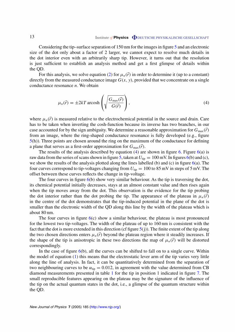
Considering the tip–surface separation of 150 nm for the images in figure 5 and an electronicsize of the dot only about a factor of 2 larger, we cannot expect to resolve much details inthe dot interior even with an arbitrarily sharp tip. However, it turns out that the resolutionis just sufficient to establish an analysis method and get a first glimpse of details withinthe QD.
For this analysis, we solve equation (2) for µn(�r) in order to determine it (up to a constant)directly from the measured conductance image G(x, y), provided that we concentrate on a singleconductance resonance n. We obtain
µn(�r) = ±2kT arcosh
√Gmax(�r)G(�r)
, (4)
where µn(�r) is measured relative to the electrochemical potential in the source and drain. Carehas to be taken when inverting the cosh-function because its inverse has two branches, in ourcase accounted for by the sign ambiguity. We determine a reasonable approximation for Gmax(�r)from an image, where the ring-shaped conductance resonance is fully developed (e.g., figure5(h)). Three points are chosen around the ring on the maximum of the conductance for defininga plane that serves as a first-order approximation for Gmax(�r).
The results of the analysis described by equation (4) are shown in figure 6. Figure 6(a) israw data from the series of scans shown in figure 5, taken at Utip = 100 mV. In figures 6(b) and (c),we show the results of the analysis plotted along the lines labelled (b) and (c) in figure 6(a). Thefour curves correspond to tip-voltages changing from Utip = 100 to 85 mV in steps of 5 mV. Theoffset between these curves reflects the change in tip-voltage.
The four curves in figure 6(b) show very similar behaviour. As the tip is traversing the dot,its chemical potential initially decreases, stays at an almost constant value and then rises againwhen the tip moves away from the dot. This observation is the evidence for the tip probingthe dot interior rather than the dot probing the tip. The appearance of the plateau in µn(�r)in the centre of the dot demonstrates that the tip-induced potential in the plane of the dot issmaller than the electronic width of the QD along this line by the width of the plateau which isabout 80 nm.
The four curves in figure 6(c) show a similar behaviour, the plateau is most pronouncedfor the lowest two tip-voltages. The width of the plateau of up to 160 nm is consistent with thefact that the dot is more extended in this direction (cf figure 5(j)). The finite extent of the tip alongthe two chosen directions enters µn(�r) beyond the plateau region where it steadily increases. Ifthe shape of the tip is anisotropic in these two directions the map of µn(�r) will be distortedcorrespondingly.
In the case of figure 6(b), all the curves can be shifted to fall on to a single curve. Withinthe model of equation (1) this means that the electrostatic lever arm of the tip varies very littlealong the line of analysis. In fact, it can be quantitatively determined from the separation oftwo neighbouring curves to be αtip = 0.012, in agreement with the value determined from CBdiamond measurements presented in table 1 for the tip in position 1 indicated in figure 7. Thesmall reproducible features appearing on the plateau may be the signature of the influence ofthe tip on the actual quantum states in the dot, i.e., a glimpse of the quantum structure withinthe QD.
New Journal of Physics 7 (2005) 185 (http://www.njp.org/)

14 Institute of Physics �DEUTSCHE PHYSIKALISCHE GESELLSCHAFT
0 100 200 300
1
2
3
4
(b)
(c)
( b )
(c)
V =100mVtip
(a)
V =100mVtip
V =100mVtip
95mV
90mV
85mV
95mV
90mV
85mV
Position of measurement (nm)
0Position of measurement (nm)
330
(b)
µ n(r
) / 2
kTµ n
(r)
/ 2kT
1
2
3160 nm
80 nm
Figure 6. Analysis of the development of µn for various Utip. µn was calculatedusing equation (4). (a) Map of µn for the image in figure 5(i) with a scan area of300 nm × 300 nm. The two lines (marked as (b) and (c)) indicate along which linesthe data were analysed. (b) Development of µn along line (b) for Utip = 85, 90, 95and 100 mV. (c) Development of µn along line (c) for the same values of Utip asin the previous case.
New Journal of Physics 7 (2005) 185 (http://www.njp.org/)

15 Institute of Physics �DEUTSCHE PHYSIKALISCHE GESELLSCHAFT
Table 1. Influence of the tip position relative to the dot on the lever arms of gatesand tip and on the charging energy e2/C� The absolute lever arms of the PG andthe charging energy e2/C� were determined directly from CB diamonds. Theabsolute lever arms of all other gates were calculated using measured relativelever arms.
Absolute lever arm
Pos. PG Tip G1 G2 e2/C� (µeV)
1 0.129 (±0.01) 0.013 (±7 × 10⁻⁴) 0.107 (±0.008) 0.065 (±0.005) 733 (±49)2 0.114 (±0.017) 0.0014 (±6 × 10⁻⁴) 0.093 (±0.008) 0.054 (±0.008) 772 (±10)3 0.138 (±0.011) 0.0017 (±4 × 10⁻⁴) 0.111 (±0.009) 0.069 (±0.007) 808 (±8)4 0.119 (±0.008) 0.0018 (±1 × 10⁻⁴) 0.101 (±0.006) 0.058 (±0.004) 786 (±12)5 0.132 0.004 0.111 0.0654 732 (±34)6 0.133 0.005 0.111 0.0653 810 (±10)7 0.096 (±0.016) 0.009 (±0.001) 0.082 (±0.014) 0.044 (±0.008) 766 (±42)
From the above analysis it becomes clear why conductance resonance features can beobserved in scanning-gate images that are much smaller than the electronic size of the QD. Thisis even the case, if the tip radius is larger than in our experiment and no plateau is observedin µn(�r). It can be easily shown from equation (2), if a parabolic approximation is made forµn(�r) around the dot centre. The size of conductance resonance rings depends in this situationon the curvature of µn(�r) where it is maximal. Sufficiently large curvature can lead to ringssmaller than the electronic size of the dot even though the full-width at half-maximum of the tip–dot interaction potential may be significantly larger. Tip-voltages closer to the contact potentialdifference lead to a smaller curvature and therefore to a larger size of comparable conductanceresonances.
4. Effects of the tip on lever arms and charging energy
As mentioned in the discussion of equation (1), it is expected that the presence of the tip close tothe QD may change the lever arms of the gates and the charging energy of the dot. We investigatedthis influence by placing the tip at several representative x–y-positions at a distance of 200 nmfrom the surface as indicated in figure 7. In each position CB diamonds were measured andthe relative lever arms of the gates were determined. The results are summarized in table 1. Asexpected, the lever arm of the tip is a strong function of its position relative to the QD. The leverarms of the gates PG, ‘G1’and ‘G2’were also found to change significantly for the tip in differentpositions giving evidence for the screening effects discussed in connection with equation (1). Therelatively unsystematic change of the lever arms with tip position is a consequence of the ratherpeculiar shape and double-tip character of this particular sensor. For a cylindrically symmetricsensor, a rather symmetric and systematic dependence of the lever arms on tip position wouldbe expected. The same argument applies to the corresponding charging energies given in the lastcolumn of table 1. The values also vary significantly from position to position although a moresymmetric and systematic dependence would be expected for a single symmetric tip.
New Journal of Physics 7 (2005) 185 (http://www.njp.org/)

16 Institute of Physics �DEUTSCHE PHYSIKALISCHE GESELLSCHAFT
1
2
3
4
56
7
Figure 7. Positions of the tip during the measurements of the tip-positiondependence of the lever arms.
5. What are the conditions for true wave function mapping?
From the above analysis it becomes clear that certain criteria need to be fulfilled for wave functionmapping in a lateral semiconductor QD. Firstly, the QD has to be operated in the single-leveltransport regime in which a single wave function dominates the conductance resonance. Thisrequires an electron temperature well below that determined in the presented experiments anddot sizes. In addition, a lithographically smaller dot would help for achieving the single-leveltransport regime by increasing the single-particle level spacing �. The second requirement forwave function mapping is a tip-diameter small compared to the Fermi wavelength which is ofthe order of 30–50 nm. Such tip-diameters were actually realized with our electrochemicallysharpened tips as confirmed by scanning electron microscopy. Thirdly, the separation betweenthe tip and the 2DEG needs to be smaller than the Fermi wavelength, i.e., shallow 2DEGs arerequired with cap layers of thickness less than 50 nm. This requirement is met in our samples.The tip–surface separation has to be minimized, but is less crucial than the cap layer thicknessdue to the high relative dielectric constant of the Ga[Al]As material.
Wave function mapping experiments would have to be performed at voltages where thetip–dot interaction is very close to the least invasive situation in order to perturb the QD wavefunctions only slightly. Highest sensitivity can be expected in the tail of a conductance peak atan operating point in PG where the slope of the conductance is maximized.
6. Conclusions
The presented scanning-gate experiment demonstrates the progress made and the problemsencountered in the local investigation of quantum states in semiconductor QDs. Many crucialrequirements such as reliable operation of the scanning probe microscope at cryogenic
New Journal of Physics 7 (2005) 185 (http://www.njp.org/)

17 Institute of Physics �DEUTSCHE PHYSIKALISCHE GESELLSCHAFT
temperatures, coarse positioning of the sample and the long-term stability of the sample duringscanning have been met. The spatial resolution has been put to its limits, so far given by the qualityof the tip, the cleanliness of the sample surface and the accessible electron temperature. Withinthese limits, the expected optimum in resolution has been demonstrated, allowing scanning-gate images within the electronic area of the QD. The results of these experiments promise thefeasibility of accessing the local quantum mechanical probability distributions of electronic statesin QD structures and even more complicated coupled mesoscopic systems. Such a technique hasthe potential to improve our abilities to design and tailor quantum states for highly demandingapplications such as quantum communication and quantum information processing.
Acknowledgments
We thank T Vancura for his contribution to the experimental setup. Financial support from theSwiss Science Foundation (Schweizerischer Nationalfonds) via NCCR Nanoscience is gratefullyacknowledged.
References
[1] Nielsn M A and Chuang I L 2000 Quantum Computation and Quantum Information (Cambridge: CambridgeUniversity Press)
[2] Quantum Information Science and Technology Roadmap, available at http://qist.lanl.gov/[3] Kouwenhoven L P, Schön G and Sohn L L 1997 NATO ASI Conf. Proc. (Dordrecht: Kluwer) pp 105–214[4] Grabert H and Devoret M H (eds) 1991 Single Charge Tunneling (New York: Plenum)[5] Fuhrer A, Lüscher S, Ihn T, Heinzel T, Ensslin K, Wegscheider W and Bichler M 2001 Nature 413 822[6] Lindemann S, Ihn T, Heinzel T, Zwerger W, Ensslin K, Maranowski K and Gossard A C 2002 Phys. Rev.
B 66 195314[7] Kyriakidis J, Pioro-Ladriere M, Ciorga M, Sachrajda A S and Hawrylak P 2002 Phys. Rev. B 66 35320[8] Hanson R, Witkamp B, Vandersypen L M, Willems van Beveren L H, Elzerman J M and Kouwenhoven L P
2003 Phys. Rev. Lett. 91 196802[9] Fuhrer A, Ihn T, Ensslin K, Wegscheider W and Bichler M 2003 Phys. Rev. Lett. 91 206802
[10] Loss D and DiVincenzo D P 1998 Phys. Rev. A 57 120[11] Burkhard G, Engel H-A and Loss D 2000 Fortschr. Phys. 48 965[12] Ciorga M, Sachrajda A S, Hawrylak P, Gould C, Zawadzki P, Jullian S, Feng Y and Wasilewski Z 2000
Phys. Rev. B 61 R16315[13] Kouwenhoven L P, Austing D G and Tarucha S 2001 Rep. Prog. Phys. 64 701[14] Hanson R, Witkamp B, Vandersypen L M K, Willems van Beveren L H, Elzerman J M and Kouwenhoven L P
2003 Phys. Rev. Lett. 91 196802[15] Zumbühl D M, Marcus C M, Hanson M P and Gossard A C 2004 Phys. Rev. Lett. 93 256801[16] Yoo M J, Fulton T A, Hess H F, Willett R L, Dunkleberger L N, Chichester R J, Pfeiffer L N and West K W
1997 Science 276 579[17] Ilani S, Martin J, Teitelbaum E, Smet J H, Mahalu D, Umansky V and Yacoby A 2004 Nature 427 328[18] Finkelstein G, Glicofridis P I, Ashoori R C and Shayegan M 2000 Science 289 90[19] Topinka M A, LeRoy B J, Westervelt R M, Shaw S E J, Fleischmann R, Heller E J, Maranowski K D and
Gossard A C 2001 Nature 410 183[20] Crook R, Smith C G, Graham A C, Farrer I, Beere H E and Ritchie D A 2003 Phys. Rev. Lett. 91 246803[21] Woodside M T and McEuen P L 2002 Science 296 1098[22] Pioda A, Kicin S, Ihn T, Sigrist M, Fuhrer A, Ensslin K, Weichselbaum A, Ulloa S E, Reinwald M and
Wegscheider W 2004 Phys. Rev. Lett. 93 216801
New Journal of Physics 7 (2005) 185 (http://www.njp.org/)

18 Institute of Physics �DEUTSCHE PHYSIKALISCHE GESELLSCHAFT
[23] Fallahi P, Bleszynski A C, Westervelt R M, Huang J, Walls J D, Heller E J, Hanson M and Gossard A C 2005Nano. Lett. 5 223
[24] Mendoza M and Schulz P A 2003 Phys. Rev. B 68 205302[25] Held R, Vancura T, Heinzel T, Ensslin K, Holland M and Wegscheider W 1998 Appl. Phys. Lett. 73 262[26] Heinzel T, Held R, Lüscher S, Ensslin K, Wegscheider W and Bichler M 2001 Physica E 9 84[27] Fuhrer A, Dorn A, Lüscher S, Heinzel T, Ensslin K, Wegscheider W and Bichler M 2002 Superlatt.
Microstruct. 31 19[28] Ihn T 2004 Electronic Transport in Mesoscopic Semiconductor Structures (Springer Tracts in Modern Physics
vol 192) (New York: Springer)[29] Beenakker C W J 1991 Phys. Rev. B 44 1646[30] Vancura T, Kicin S, Ihn T, Ensslin K, Bichler M and Wegscheider W 2003 Appl. Phys. Lett. 83 2602
New Journal of Physics 7 (2005) 185 (http://www.njp.org/)