Embed Size (px)
Citation preview
New Design Approach of Antennas with
Integrated Coupled Resonator Filters
Ekasit Nugoolcharoenlap
A thesis submitted to the University of Birmingham for the degree of Doctor of Philosophy
School of Electronic, Electrical and System Engineering
The University of Birmingham
March 2015

University of Birmingham Research Archive
e-theses repository This unpublished thesis/dissertation is copyright of the author and/or third parties. The intellectual property rights of the author or third parties in respect of this work are as defined by The Copyright Designs and Patents Act 1988 or as modified by any successor legislation. Any use made of information contained in this thesis/dissertation must be in accordance with that legislation and must be properly acknowledged. Further distribution or reproduction in any format is prohibited without the permission of the copyright holder.
Abstract
In the majority of microwave receiving and transmitting systems, a requirement is to
have a filter immediately adjacent to the antenna or antenna array. Conventionally the filter
and antenna are designed as separate components and a matching circuit is used in order to
get maximum power transfer between them. This thesis presents a new methodology for
antenna design where a filter is either fully or partially integrated with the antenna elements.
The design of this antenna-filter follows the well-established coupled-resonator filter design
theory, in which each resonator can not only be used as a filter element but also as a radiator.
In order to verify the concept, dipole antennas have been employed as antenna
elements, and in addition to their radiating properties they are treated as the resonators in the
filter circuit. For this purpose, an inductor has been integrated with each dipole antenna
forming the resonator circuit. A two-port bandpass filter designed using dipole antennas is the
first work in this thesis to verify the use of dipole antennas as resonators; this confirms the
design concepts. The coupling matrix has been used to obtain the filter response. Further work
demonstrates one-port antenna-filters made out of one, two and three dipoles; in these cases
the designed filtering response uses the dipoles as resonators as well as radiating elements.
The simulation and measurement results are in good agreement.
The method has also been utilised to implement X-band waveguide antenna
components, here the radiation is from the open end of a waveguide. An antenna-filter,
antenna-power divider and an antenna-diplexer are all demonstrated. The antenna-filter is
designed for improve the selectivity. The other two components are three-port components
and designed using the coupling matrix. The antenna power divider is designed so that the
radiation pattern can be controlled in addition to providing the filtering. The antenna-diplexer

is designed in order to include the radiation element into a structure which also provides
power splitting at two different frequencies. These three variations of the waveguide antenna-
filter has been designed, simulated, fabricated and measured. The results are in good
agreement. They have provided verification of the method, showing the antenna and filter
theories and can be applied to miniaturise these components. The results have application in
the wireless communication and radar systems.

Acknowledgements
I am extremely grateful for the guidance and support of my supervisors Prof. Michael
Lancaster and Dr. Frederick Huang. They gave me many important advices and helpful
suggestions during my study.
My appreciation also goes to my colleagues in the Emerging Device Technology for their
support and friendship (EDT) Research Group at the University of Birmingham. Especially,
I would like to thanks Dr. Xiaobang Shang for many helpful suggestions during my study,
Wenlin Xia for helpful discussion on the filter design, Rashad Hassan Mahmud for helpful
discussion on the antenna theory and David Glynn for helpful discussion on thesis writing.
I am also thankful Mr. Warren Hay for fabricating all the waveguide devices presented in this
thesis.
I appreciate Dr. Ghaith Elsanosi M. Mansour and Dr. Zhen Hua Sampson Hu. They gave
many advices for the antenna measurement technique. Thanks to Dr. Khurram Saleem
Alimgeer in many suggestions for doing the research work during his visited time.
Finally, my sincere gratitude goes to my parents for their invaluable support and
encouragement. I also appreciate the Royal Thai Government for financial and general
supports until course end.

Table of Contents
Chapter 1: Introduction.................................................................................. 1
1.1 Overview of Integration of the Antenna and Bandpass Filter Components................ 1
1.2 Literature review.......................................................................................................... 4
1.3 Thesis Motivation........................................................................................................ 8
1.4 Thesis Overview.......................................................................................................... 10
References.......................................................................................................................... 11
Chapter 2: Fundamental Theory.................................................................. 16
2.1 Antenna Theory.......................................................................................................... 16
2.1.1 Overview of Antennas....................................................................................... 16
2.1.2 Dipole Antennas................................................................................................ 21
2.1.2.1 Equivalent Circuit of Dipole Antenna.................................................. 25
2.1.2.2 Quality Factor of Dipole Antenna........................................................ 31
2.1.3 Waveguide Aperture Antennas......................................................................... 33
2.2 Microwave Filter Theory........................................................................................... 34
2.2.1 Overview of Microwave Filters........................................................................ 34
2.2.2 Microwave Resonators...................................................................................... 39
2.2.3 Rectangular Waveguide Cavity Resonator........................................................ 41
2.2.4 Coupled Resonator Filters................................................................................. 44
2.2.5 Coupling Matrix for Coupled Resonator Filters................................................ 45
2.3 Coupling Matrix for Antenna-Filters.......................................................................... 53
2.4 CST Microwave Studio............................................................................................. 55
2.4.1 CST Microwave Studio Overview................................................................... 56

2.4.2 Instruction for using CST Microwave Studio................................................ 56
References....................................................................................................................... 64
Chapter 3: Two-Port Dipole Bandpass Filter ............................................. 66
3.1 Introduction............................................................................................................... 66
3.2 Resonator Design...................................................................................................... 67
3.2.1 Equivalent Circuit of Dipole Antenna in Simulation....................................... 67
3.2.2 Design of Dipole Antenna with Inductor......................................................... 70
3.2.3 Unloaded Quality Factor.................................................................................. 73
3.3 Design of Two-Port Dipole Bandpass Filter............................................................. 73
3.4 Realisation of Two-Port Dipole Bandpass Filter...................................................... 76
3.4.1 Air Coil Inductor Design................................................................................. 76
3.4.2 Extraction of External Quality Factor............................................................. 79
3.4.3 Extraction of Coupling Coefficient................................................................. 81
3.4.4 Simulation Results........................................................................................... 82
3.4.5 Fabrication and Measurement.......................................................................... 85
3.5 Conclusions............................................................................................................... 87
References....................................................................................................................... 88
Chapter 4: One-Port Dipole Antenna-Filter............................................... 89
4.1 Introduction............................................................................................................... 89
4.2 One-Resonator Dipole Antenna-Filter...................................................................... 90
4.2.1 Antenna-Filter Design...................................................................................... 90
4.2.2 Extraction of Design Parameters from Physical Structure............................... 91
4.2.3 Calculation and Simulation Results................................................................. 95
4.2.4 Fabrication and Measurement.......................................................................... 96
4.3 Two-Resonator Dipole Antenna-Filter................................................................... 100
4.3.1 Antenna-Filter Design.................................................................................... 100
4.3.2 Calculation and Simulation Results............................................................... 104
4.3.3 Fabrication and Measurement........................................................................ 106
4.4 Three-Resonator Dipole Antenna-Filter................................................................. 109
4.4.1 Antenna-Filter Design................................................................................... 109
4.4.2 Calculation and Simulation Results.............................................................. 113
4.4.3 Fabrication and Measurement....................................................................... 114
4.5 Conclusions............................................................................................................ 125
References.................................................................................................................... 126
Chapter 5: Waveguide Antenna-Filters..................................................... 127
5.1 Introduction............................................................................................................ 127
5.2 Quality Factors of Cavity Resonators.................................................................... 129
5.2.1 Extraction of the External Quality Factor from Physical Structure.............. 130
5.3 Waveguide Aperture Antennas............................................................................... 133
5.4 Coupling Coefficient Extraction from the Physical Structure................................ 135
5.5 Coupling Matrix Synthesis for Multiple Port Antenna-Filters............................... 137
5.6 X-Band 5-Resonator Waveguide Antenna-Filter.................................................... 139
5.6.1 Waveguide Antenna-Filter Design................................................................. 139
5.6.2 Fabrication and Measurement........................................................................ 143
5.7 X-band 3-Resonator Antenna Power Divider......................................................... 146
5.7.1 Waveguide Antenna Power Divider Design.................................................. 146
5.7.2 Fabrication and Measurement........................................................................ 149
5.8 X-Band 3-Resonator Antenna-Diplexer................................................................. 153
5.8.1 Waveguide Antenna-Diplexer Design........................................................... 153
5.8.2 Fabrication and Measurement........................................................................ 157
5.9 Conclusions............................................................................................................. 161
References..................................................................................................................... 162
Chapter 6: Conclusions and Future Work................................................ 163
6.1 Conclusions............................................................................................................. 163
6.2 Future Work............................................................................................................ 165
References..................................................................................................................... 168
Appendix A: Q-calculation for the one-port component.......................... 169
References...................................................................................................................... 173
Appendix B: Publications …………………………................................... 174
1
Chapter 1
Introduction
1.1 Overview of Integration of Antenna and Bandpass Filter Components
Recently attention in the design of microwave circuits has been directed towards
miniaturisation and low profile for components in wireless communication systems. An
antenna and a bandpass filter are essential components employed at the front-ends. Examples
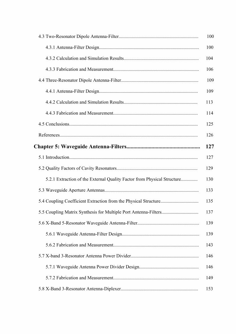
of the use of an antenna and a bandpass filter at the front-end of Radio Frequency (RF)
transmitter and receiver are shown in Figure 1.1. For the transmitter shown in Figure 1.1(a), a
bandpass filter follows a power amplifier and used for selecting a transmission frequency and
rejecting out of band frequency before being sent to an antenna for broadcasting the RF
signal. On the other hand, an antenna is the first device of the receiving system as shown in
Figure 1.1(b). The antenna is placed at the front of the receiver to receive the RF signal and
sent to a bandpass filter. It also acts as a pre-selector for the reception carrier frequency to the
input of a low-noise amplifier. This arrangement of the antenna and filter reduces noise and
interference before converting lower frequency by mixer and oscillator [1]. However, a
degradation of the front-end performance is caused by mismatched impedance of an antenna
and a bandpass filter. A matching network [1] is therefore needed for the front-end circuit to
match impedance between antenna and filter. The matching network may improve the
performance of the systems, but the circuit size may also be increased. In general, bandpass
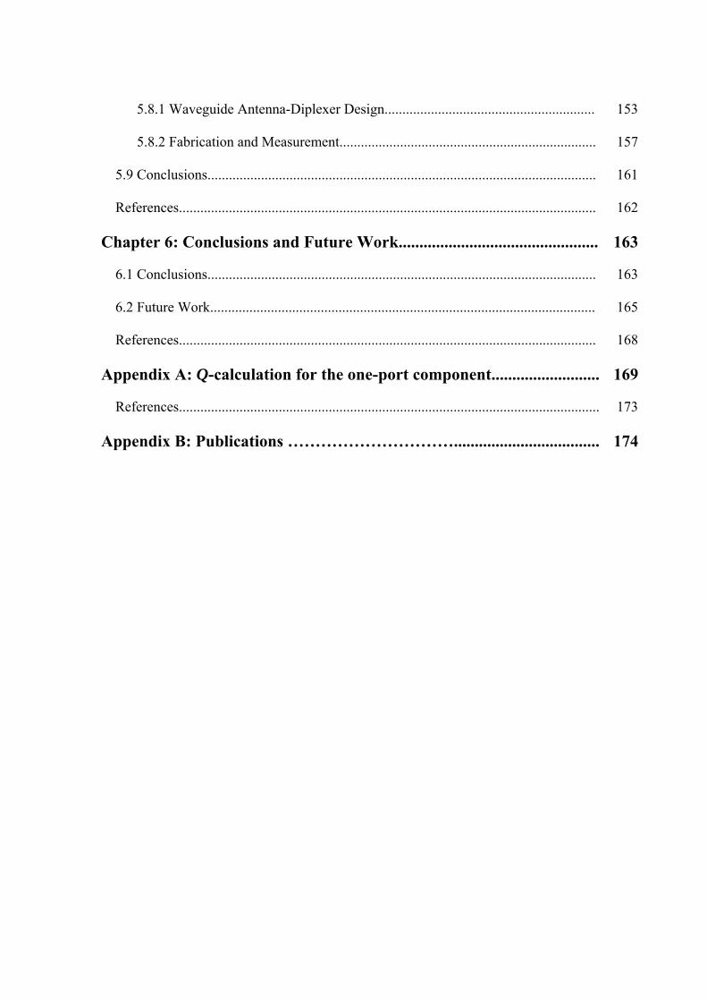
filters are designed based on coupled resonator circuits. This bandpass filter is named a
coupled resonator filter [2]. Figure 1.2 shows an example diagram of nth order coupled-
2
resonator bandpass filter, where white circles represent resonators, and the solid lines linking
resonators represent coupling.
(a)
(b)
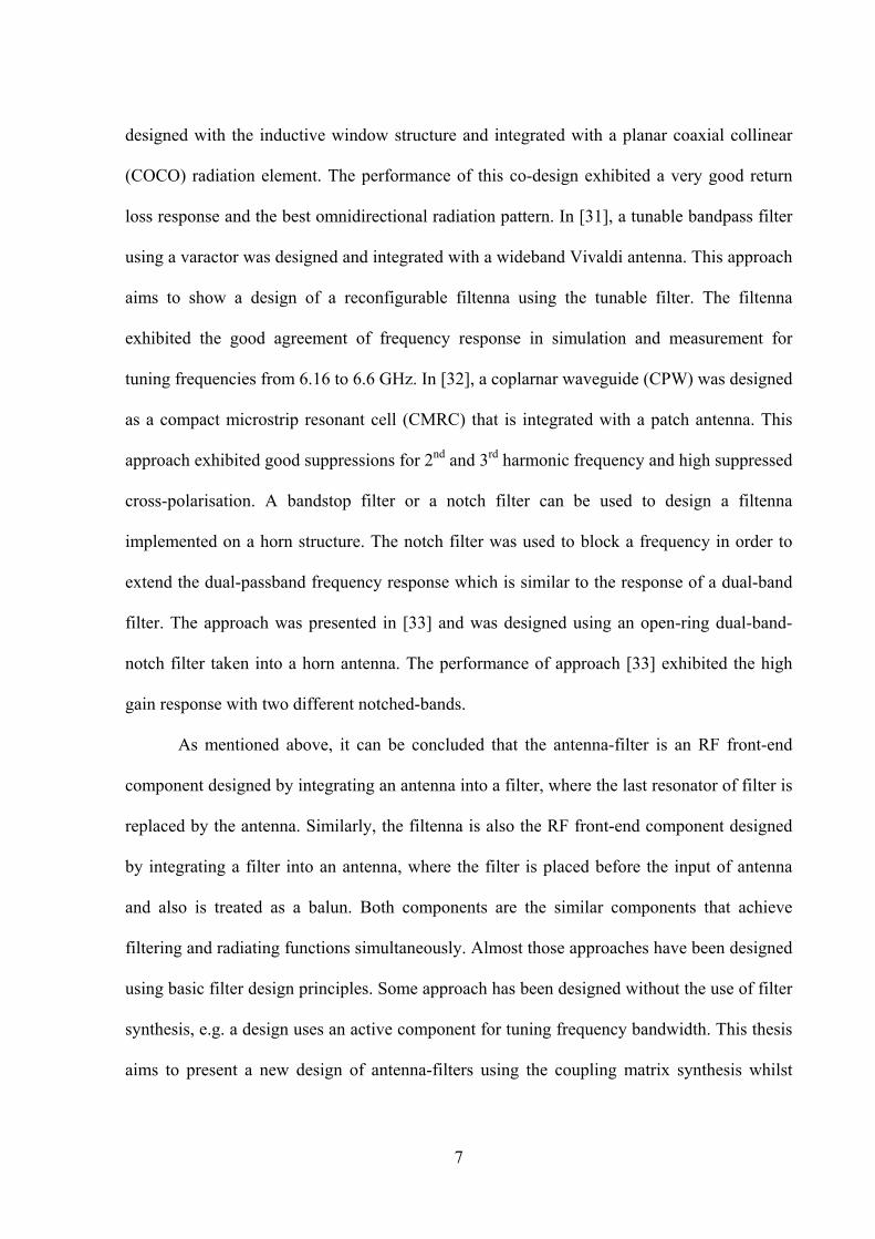
Figure 1.1 Block diagram of (a) An RF transmitter and (b) Block diagram of an RF receiver
[1].
Figure 1.2 An example diagram of nth order coupled-resonator bandpass filter.
As mentioned above, the main function of an antenna is to radiate the RF signal to free space.
It can also act as a resonator of the filter when it resonates at the operating frequency. It is
possible to demonstrate the relation of antenna and resonator by analysing and comparing the
resonant antenna circuit (i.e. the reactance (X) or the susceptance (B) of the reactive element is
3
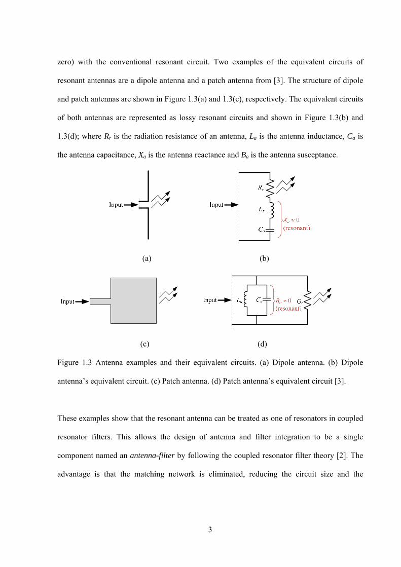
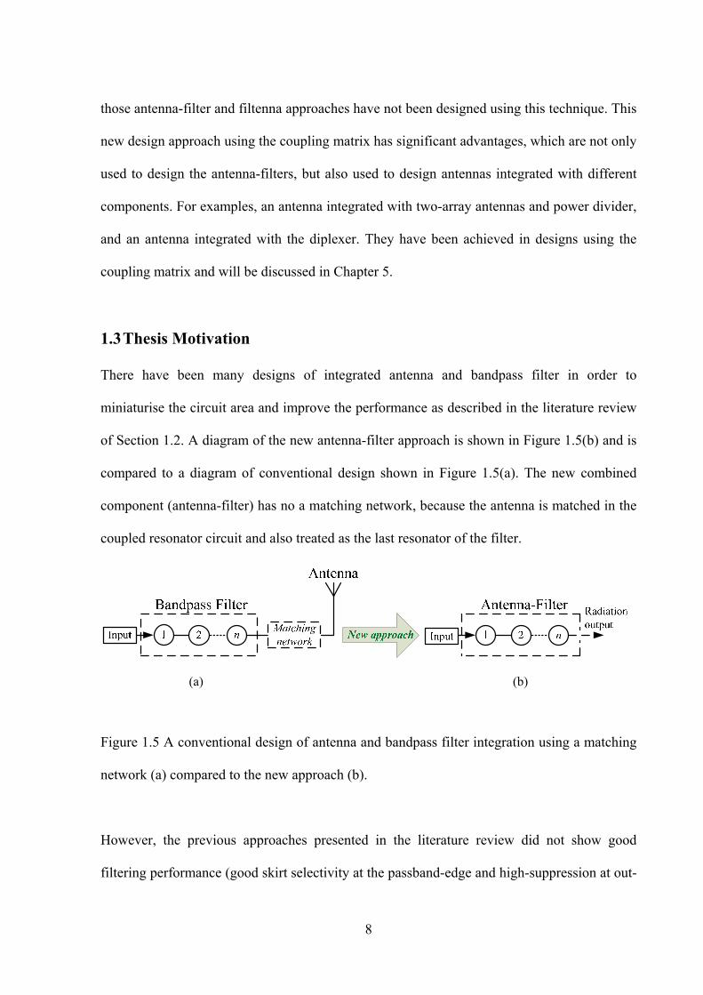
zero) with the conventional resonant circuit. Two examples of the equivalent circuits of
resonant antennas are a dipole antenna and a patch antenna from [3]. The structure of dipole
and patch antennas are shown in Figure 1.3(a) and 1.3(c), respectively. The equivalent circuits
of both antennas are represented as lossy resonant circuits and shown in Figure 1.3(b) and
1.3(d); where Rr is the radiation resistance of an antenna, La is the antenna inductance, Ca is
the antenna capacitance, Xa is the antenna reactance and Ba is the antenna susceptance.
(a) (b)
(c) (d)
Figure 1.3 Antenna examples and their equivalent circuits. (a) Dipole antenna. (b) Dipole
antenna’s equivalent circuit. (c) Patch antenna. (d) Patch antenna’s equivalent circuit [3].
These examples show that the resonant antenna can be treated as one of resonators in coupled
resonator filters. This allows the design of antenna and filter integration to be a single
component named an antenna-filter by following the coupled resonator filter theory [2]. The
advantage is that the matching network is eliminated, reducing the circuit size and the
4
problem of a connection between antenna and bandpass filter. This is the main work and will
be discussed in this thesis.
1.2 Literature Review
This section presents a literature review of antenna-filter approaches. In general, the
antenna-filter is usually designed using a matching network to cascade between an antenna
and a bandpass filter as described in the previous section. The design approaches using the
matching network were presented in [4], [5]. The advantage of the method is to enhance the
bandwidth of the microstrip antenna. A design approach of the antenna and filter integration
without the matching network has been firstly presented in [6] with the use of the filter
synthesis. The method was to consider an antenna as equivalent to a last resonator in the filter
circuit. This has been used to implement a slot-line dipole antenna with a coplanar filter. The
approached design can improve the filtering response by tuning the radiation resistance of the
resonant antenna to match the load resistance of filter circuits at the resonant frequency. In
addition, the filter synthesis has been implemented on the various structures for size
reduction, e.g. [7], [8] which show a microstrip filter integrated with a patch antenna, an E-
plane waveguide filter integrated with a patch antenna [9]. A multilayer technology is of
interest to RF circuit designer and can be employed to miniaturise the RF circuits and
integrate RF components into a single module. In [10], a composite ceramic-foam substrate
with the multilayer technology has been implemented to design a microstrip patch antenna
integrated with a filter. A similar concept in [6] is employed to design the antenna-filter
component. Moreover, the approach [10] has firstly introduced the design of antenna-filter
using the principle of the coupled-resonator filter design. The design method was simple by
5
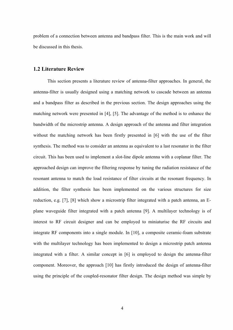
considering the quality factor of the antenna as the same external quality factor of the last
resonator of filter circuits. The circuit diagram of the approach in [10] is shown in Figure 1.4.
Figure 1.4 The diagram of the antenna integrated in the bandpass filter circuits [10].
A cavity filter integrated into a horn antenna has been presented in [11]. This work exhibited a
good two-pole filter response and radiation pattern shape. The integration of ultra-wide band
(UWB) antenna with a filter was presented in [12], [13]. These approaches have been
implemented on the planar structure in order to miniaturise the size. In [14], the design of a
patch antenna integrated with the folded step-impedance resonator (SIR) filter can be applied
to reject the unwanted harmonic response. In [15], multi-layer circuit technology has been
used to implement a multi-layer antenna-filter structure. The approach [15] has been used to
design a hairpin filter positioned at the bottom layer combined with the patch antenna placed
on the top layer of the component. This work exhibited a two-pole response and well-shaped
radiation pattern. In [16], the design approach presented the dual-band filter integrated with
the dual-band patch antenna. This component was designed for use in the modern wireless
system, e.g. the wireless LAN system. The concept of filter design has again been utilised
with the co-design of antenna and filter integration. The co-design approaches were
implemented on the microstrip filter with an inverted-L antenna [17], the microstrip filter with
-shaped antenna [18], the substrate-integrated waveguide (SIW) filters with patch antenna
6
[19], the waveguide slot antenna with integrated filters [20], the aperture evanescent
waveguide antenna with filter [21], [22], and the integration of aperture antenna and filter for
the SIW structure [23].
Antenna arrays can be used to improve radiation performance compared with single
antennas. The antenna array has been incorporated with the antenna-filter design for various
structures. For example, four-slot antenna arrays integrated with cavity filters [24], Yagi
antenna combined with a high Q-resonator [25] and four-patch antenna array integrated with
power dividers and filters [26]. In addition, it is possible to design the antenna and filter with
multi-band response. Previously, a dual-band antenna has been designed with an integrated
diplexer and presented in [27]. The approach exhibited a new combined component for the
transceiver of the wireless LAN system with a compact size and good filter performance. In
[28], the microstrip patch antenna was designed and combined with two bandpass filters to
create a single module.
A type of antenna with filtering function has been presented in [29] and is called a
filtering antenna or a filtenna. This component is designed by integrating a bandpass filter
into an antenna in order to enhance the filtering functionality of the antenna. Also cost and
size reductions are required for the component. Following the filtenna's design concept, the
gain response of filtenna can exhibit flat in-band gain, high out of band gain suppression and
high harmonic rejection. The approach presented in [29] aims to show a design technique of
filtenna implemented on horn structure by covering a substrate integrated waveguide cavity
(SIWC) FSS filter at the aperture of a horn antenna. The SIWC-FSS acts as a frequency
selector placed at the aperture to suppress the unwanted frequency from the received signals
before being sent to the input of receiver. This component is suitably utilised as a receiving
antenna. The planar filtennas have been presented in [30]-[32]. In [30], an SIW filter was
7
designed with the inductive window structure and integrated with a planar coaxial collinear
(COCO) radiation element. The performance of this co-design exhibited a very good return
loss response and the best omnidirectional radiation pattern. In [31], a tunable bandpass filter
using a varactor was designed and integrated with a wideband Vivaldi antenna. This approach
aims to show a design of a reconfigurable filtenna using the tunable filter. The filtenna
exhibited the good agreement of frequency response in simulation and measurement for
tuning frequencies from 6.16 to 6.6 GHz. In [32], a coplarnar waveguide (CPW) was designed
as a compact microstrip resonant cell (CMRC) that is integrated with a patch antenna. This
approach exhibited good suppressions for 2nd and 3rd harmonic frequency and high suppressed
cross-polarisation. A bandstop filter or a notch filter can be used to design a filtenna
implemented on a horn structure. The notch filter was used to block a frequency in order to
extend the dual-passband frequency response which is similar to the response of a dual-band
filter. The approach was presented in [33] and was designed using an open-ring dual-band-
notch filter taken into a horn antenna. The performance of approach [33] exhibited the high
gain response with two different notched-bands.
As mentioned above, it can be concluded that the antenna-filter is an RF front-end
component designed by integrating an antenna into a filter, where the last resonator of filter is
replaced by the antenna. Similarly, the filtenna is also the RF front-end component designed
by integrating a filter into an antenna, where the filter is placed before the input of antenna
and also is treated as a balun. Both components are the similar components that achieve
filtering and radiating functions simultaneously. Almost those approaches have been designed
using basic filter design principles. Some approach has been designed without the use of filter
synthesis, e.g. a design uses an active component for tuning frequency bandwidth. This thesis
aims to present a new design of antenna-filters using the coupling matrix synthesis whilst
8
those antenna-filter and filtenna approaches have not been designed using this technique. This
new design approach using the coupling matrix has significant advantages, which are not only
used to design the antenna-filters, but also used to design antennas integrated with different
components. For examples, an antenna integrated with two-array antennas and power divider,
and an antenna integrated with the diplexer. They have been achieved in designs using the
coupling matrix and will be discussed in Chapter 5.
1.3 Thesis Motivation
There have been many designs of integrated antenna and bandpass filter in order to
miniaturise the circuit area and improve the performance as described in the literature review
of Section 1.2. A diagram of the new antenna-filter approach is shown in Figure 1.5(b) and is
compared to a diagram of conventional design shown in Figure 1.5(a). The new combined
component (antenna-filter) has no a matching network, because the antenna is matched in the
coupled resonator circuit and also treated as the last resonator of the filter.
(a) (b)
Figure 1.5 A conventional design of antenna and bandpass filter integration using a matching
network (a) compared to the new approach (b).
However, the previous approaches presented in the literature review did not show good
filtering performance (good skirt selectivity at the passband-edge and high-suppression at out-
9
of-band) or good radiating performance (high antenna gain and well-shaped radiation pattern).
The main reasons for the problems in the antenna-filter approaches are (i) Poor match of
antenna to filter (ii) inaccurate values of the coupling coefficient and the external quality
factor in the design, and (iii) a small number of antenna elements which cannot enhance the
antenna gain.
This thesis addresses the development of a novel antenna-filter design technique based
on the coupled resonator filter using the coupling matrix synthesis. This technique will reduce
the complexity in the design procedure, enhance the design accuracy and allow more complex
antenna-filters to be designed. As a first step, dipole antennas are chosen with inductors
completing the resonator circuits. The proposed dipole antennas, integrated with inductors,
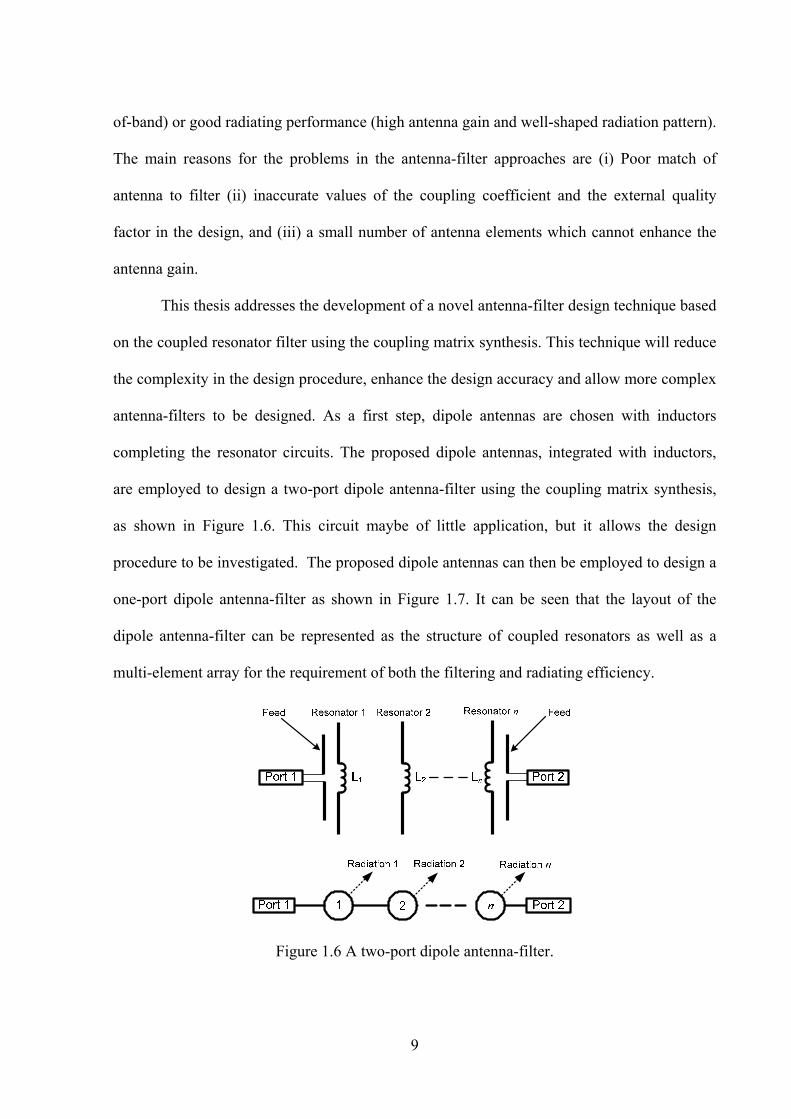
are employed to design a two-port dipole antenna-filter using the coupling matrix synthesis,
as shown in Figure 1.6. This circuit maybe of little application, but it allows the design
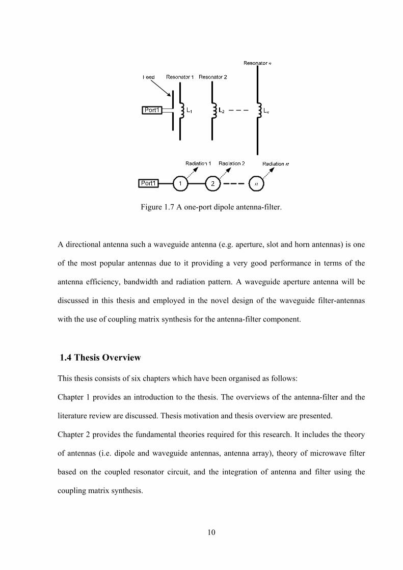
procedure to be investigated. The proposed dipole antennas can then be employed to design a
one-port dipole antenna-filter as shown in Figure 1.7. It can be seen that the layout of the
dipole antenna-filter can be represented as the structure of coupled resonators as well as a
multi-element array for the requirement of both the filtering and radiating efficiency.
Figure 1.6 A two-port dipole antenna-filter.
10
Figure 1.7 A one-port dipole antenna-filter.
A directional antenna such a waveguide antenna (e.g. aperture, slot and horn antennas) is one
of the most popular antennas due to it providing a very good performance in terms of the
antenna efficiency, bandwidth and radiation pattern. A waveguide aperture antenna will be
discussed in this thesis and employed in the novel design of the waveguide filter-antennas
with the use of coupling matrix synthesis for the antenna-filter component.
1.4 Thesis Overview
This thesis consists of six chapters which have been organised as follows:
Chapter 1 provides an introduction to the thesis. The overviews of the antenna-filter and the
literature review are discussed. Thesis motivation and thesis overview are presented.
Chapter 2 provides the fundamental theories required for this research. It includes the theory
of antennas (i.e. dipole and waveguide antennas, antenna array), theory of microwave filter
based on the coupled resonator circuit, and the integration of antenna and filter using the
coupling matrix synthesis.
11
Chapter 3 presents a new design technique of resonators using dipole antennas. The technique
is based on the antenna theory utilised to analyse the equivalent circuit of dipole antennas [3].
Inductors are employed with dipole antennas in order to complete to the resonator circuit. It
can be achieved by designing a bandpass filter using dipole antennas with inductors based on
the design of a direct-coupled resonator filter [34]. The coupling matrix is employed for this
approach with the comparison of S-parameters. The fabrication and measurement are also
provided.
Chapter 4 uses a similar design technique to that described in Chapter 3. This is intended to
design an antenna-filter as a single-port component with new coupling matrix synthesis. The
synthesis was derived from the equivalent circuit of the antenna-filter as described in Chapter
2. The approach for the work in this chapter has completed in fabrication for the single, two
and three resonator dipole antenna-filters.
Chapter 5 is the continuation of the work presented in chapter 4 which is employed to design
a waveguide antenna integrated with a cavity filter. This work is presented to show different
coupling topologies of the antenna-filter integrated with the physical structure of the
rectangular waveguide. The approach for this work has been used to implement three new
designs, which consist of five-resonator antenna-filter, three-resonator antenna power divider
and three-resonator antenna-diplexer.
Chapter 6 concludes the thesis with inclusion of the future work.
References
[1] Pozar D. M. Microwave Engineering. 3rd ed. USA: John Wiley & Sons; 2005.
[2] Hong J. S. and Lancaster M. J. Microstrip Filters for RF/Microwave Applications. New
York, USA: John Wiley & Sons; 2001.
12
[3] Balanis C. A. Antenna Theory Analysis and Design. 3rd ed. New Jersey, USA: John
Wiley & Sons; 2005.
[4] Pues, H.F., Van de Capelle, AR., An impedance-matching technique for increasing the
bandwidth of microstrip antennas. IEEE Trans. Antennas Propag., 1989 Nov., 37(11):
1345–1354.
[5] An H., Nauwelaers B., Van de Capelle A., A new approach of broadband microstrip
antenna design. in IEEE Antennas & Propag. Soc. Int. Symp., 1992 Jun. 18–25: 475–478.
[6] Le Nadan T., Coupez J.P., Toutain S., C. Person, Integration of an Antenna/Filter Device,
using a Multi-Layer, Multi-Technology Process. in 28nd Eur. Microw. Conf., 1998 Oct.:
672–677.
[7] Abbaspour-Tamijani A., Rizk J., Rebeiz G., Integration of Filters and Microstrip
Antennas. in IEEE Int. Antennas Propag. Symp. Dig., 2002 Jun.: 874–877.
[8] Queudet F., Pele I., Froppier B., Mahe Y., and Toutain S., Integration of pass-band filters
in patch antennas. in Proc. 32nd Eur. Microw. Conf., 2002 Sep. 23–26: 685–688.
[9] Goussetis G. and Budimir D., Antenna filter for modern wireless systems. in Proc. 32nd
Eur. Microw. Conf., 2002 Sep. 23–26: 1–3.
[10] Le Nadan T., Coupez J.P., Person C., Optimization and miniaturization of a filter/antenna
multi-function module using a composite ceramic-foam substrate. in Microwave Symp.
Dig., 1999 Jun. 13–19: 219–222.
[11] Froppier B., Mahe Y., Cruz E. M. and Toutain S., Integration of a filtering function in an
electromagnetic horn. in 33rd Eur. Microw. Conf., 2003 Oct. 7–9: 939–942.
[12] Lee J.N., Yoo J.H., Kim J.H., Park J.K., Kim J.S., The Design of UWB Bandpass Filter-
Combined Ultra-Wide Band Antenna. in Vehi. Tech. Conf., 2008 Sep. 21–24: 1–5.
13
[13] Yilin C. and Yonggang Z., Design of a filter-antenna subsystem for UWB
communications. in 3rd IEEE Int. Symp. on Mic., Ant., Prop. and EMC Tech. for
Wireless Comm., 2009 Oct. 27–29: 593–595.
[14] Zayniyev D. and Budimir D., An integrated antenna-filter with harmonic rejection. in 3rd
Eur. Conf. on Anten. and Propag., 2009 Mar. 23–27: 393–394.
[15] Jianhong Z., Xinwei C., Guorui H., Li L. and Wenmei Z., An Integrated Approach to RF
Antenna-Filter Co-Design. IEEE Antennas and Wireless Propagation Letters, 2009, 8:
141–144.
[16] Zayniyev D. and Budimir D., Dual-band microstrip antenna filter for wireless
communications. in IEEE Anten. and Propag. Soc. Int. Symp. (APSURSI), 2010 Jul. 11–
17: 1–4.
[17] Chuang C.-T. and Chung S.-J., Synthesis and Design of a New Printed Filtering Antenna.
IEEE Trans. Antennas Propag., 2011 Mar., 59(3): 1036–1042.
[18] Wu W.-J., Yin Y.-Z., Zuo S.-L., Zhang Z.-Y., Xie J.-J., A new compact filter-antenna for
morden wireless communication systems. IEEE Antennas Wireless Propag. Lett., 2011
Oct., 10: 1131–1134.
[19] Yusuf Y., Cheng H., Gong X., Co-Designed substrate-Integrated Waveguide Filters with
Patch Antennas. IET J. Microw., Antennas, Propag., 2013 May., 7(7): 493–501.
[20] Yang Y. and Lancaster M., Waveguide slot antenna with integrated filters. presented at
the ESA Workshop on Antennas for Space Applications, Noordwijk, Netherlands, 2010
Oct.: 48–54.
[21] Ludlow P. and Fusco V., Reconfigurable small-aperture evanescent waveguide antenna.
IEEE Trans. Antennas Propag., 2011 Dec., 59(12): 4815–4819.
14
[22] Ludlow P., Fusco V., Goussetis G. and Zelenchuk D. E., Small Aperture Evanescent-
mode waveguide antenna matched using distributed s. Electron. Lett., 2013 Apr., 49(9):
580–581.
[23] Yusuf Y., Gong X., Integration of three-dimensional high-Q filters with aperture antennas
and bandwidth enhancement utilising surface waves. IET J. Microw., Antennas, Propag.,
2013 May, 7(7): 468–475.
[24] Cheng H. T., Yusuf Y., and Gong X., Vertically integrated three-pole filter/antennas for
array applications. IEEE Antennas Wireless Propag. Lett., 2011, 10: 278–281.
[25] Wang Z., Hall P. S., Gardner P., Yagi antenna with frequency domain filtering
performance. in IEEE Antennas & Propag. Soc. Int. Symp., 2012 Jul.: 1–2.
[26] Lin C.-K. and Chung S.-J., A filtering microstrip antenna array, IEEE Trans. Microw.
Theory Tech. 2011 Nov., 59(11): 2856–2863.
[27] Demir V., Huang C. P., Elsherbeni A., Novel Dual-Band WLAN Antennas with
Integrated Band-Select Filter For 802.11 a/b/g WLAN Radios In Portable Devices.
Microw. & Opt. Technol. Lett., 2007 Aug., 49(8): 1868–1872.
[28] Zayniyev D., AbuTarboush H. F., Budimir D., Microstrip Antenna Diplexers for Wireless
Communications. in Proc. 39th Eur. Microw. Conf., 2009 Sep. 29–Oct. 1: 1508–1510.
[29] Luo G.-Q., Hong W., Tang H.-J., Chen J.-X., Yin X.-X., Kuai Z.-Q., Wu.K. Filtenna
Consisting of Horn Antenna and Substrate Integrated Waveguide Cavity FSS. IEEE
Trans. Antennas Propag., 2007 Jan., 55(1): 92–98.
[30] Yu C., Hong W., Zhenqi K., Wang H. Ku-Band Linearly Polarized Omnidirectional
Planar Filtenna. IEEE Antennas and Wireless Propagation Letters, 2012, 11: 310–313.
[31] Tawk Y., Costantine J., Christodoulou, C.G. A Varactor-Based Reconfigurable Filtenna.
IEEE Antennas and Wireless Propagation Letters, 2012, 11: 716–719.

15
[32] Ma Z., Vandenbosch, G.A.E. Wideband Harmonic Rejection Filtenna for Wireless Power
Transfer. IEEE Trans. Antennas Propag., 2014 Jan., 62(1): 371–377.
[33] Barbuto M., Trotta F., Bilotti F., Toscano A. Horn Antennas With Integrated Notch
Filters. IEEE Trans. Antennas Propag., 2015 Feb., 62(2): 781–785.
[34] Cohn S. B. Direct-Coupled-Resonator Filters. Proceedings of the IRE. 1957 Feb.; 45(2):
187–196.
16
Chapter 2
Fundamental Theory
This chapter presents a review of the relevant theory in three topic areas, firstly basic antenna
theory, secondly microwave filter theory and the thirdly integration of antenna and filter. Each
will be studied ready for the new design approaches presented in this thesis. Section 2.1
reviews the antenna theory used in the proposed design for the dipole antenna and aperture
antenna. Section 2.2 reviews the microwave filter theory to introduce the filter concept. Both
antenna and filter theories can be applied in the design of an antenna-filter presented in this
thesis. Section 2.3 presents the coupling matrix for antenna-filter utilised for the design
approaches in this thesis. CST microwave studio software instruction is also provided and is
presented in Section 2.4.
2.1 Antenna Theory
2.1.1 Overview of Antennas
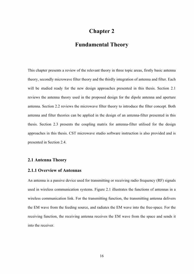
An antenna is a passive device used for transmitting or receiving radio frequency (RF) signals
used in wireless communication systems. Figure 2.1 illustrates the functions of antennas in a
wireless communication link. For the transmitting function, the transmitting antenna delivers
the EM wave from the feeding source, and radiates the EM wave into the free-space. For the
receiving function, the receiving antenna receives the EM wave from the space and sends it
into the receiver.
17
Figure 2.1 An example showing the antennas function in a wireless communication link [1].
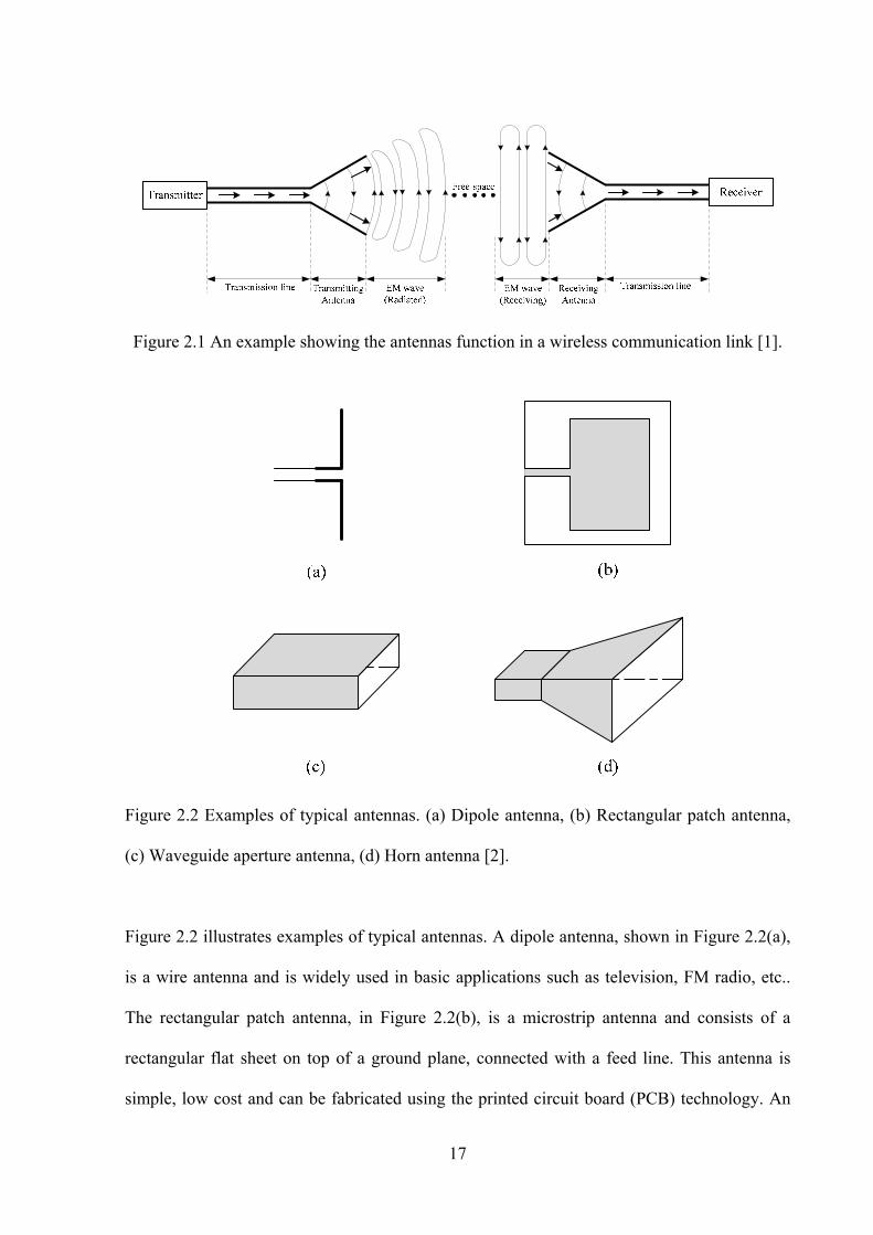
Figure 2.2 Examples of typical antennas. (a) Dipole antenna, (b) Rectangular patch antenna,
(c) Waveguide aperture antenna, (d) Horn antenna [2].
Figure 2.2 illustrates examples of typical antennas. A dipole antenna, shown in Figure 2.2(a),
is a wire antenna and is widely used in basic applications such as television, FM radio, etc..
The rectangular patch antenna, in Figure 2.2(b), is a microstrip antenna and consists of a
rectangular flat sheet on top of a ground plane, connected with a feed line. This antenna is
simple, low cost and can be fabricated using the printed circuit board (PCB) technology. An
18
open-ended waveguide antenna shown in Figure 2.2(c), is Type of aperture antenna and is
configured so the direction of EM radiation direction is based on the orientation of the
waveguide propagation mode (normally TE10 mode). This antenna is simple, efficient and can
also be installed on the surface of the spacecraft or aircraft [2]. A horn antenna, shown in
Figure 2.2(d), is also a waveguide aperture antenna that has a large aperture at the end for
improving the antenna gain and radiation patterns.
(a)
(b)
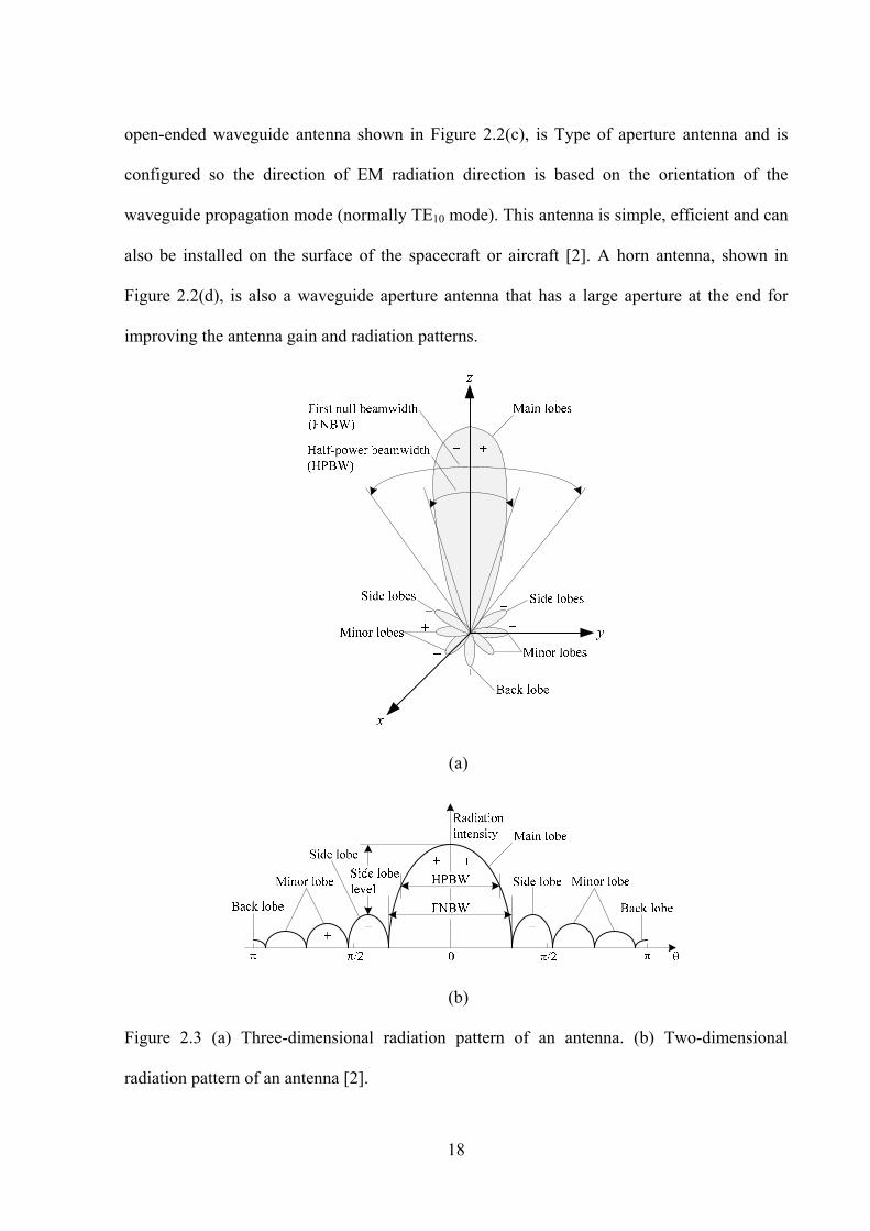
Figure 2.3 (a) Three-dimensional radiation pattern of an antenna. (b) Two-dimensional
radiation pattern of an antenna [2].
19
The performance of antennas can be described in terms of bandwidth, radiation
patterns, directivity, efficiency and gain. Figure 2.3 illustrates a typical radiation pattern of an
antenna. The lobes of the radiation pattern have different shapes, and can be divided into:
main, minor, side and back lobes [2]. The main lobe represents direction of the maximum
radiation intensity of an antenna. The half-power beam width (HPBW) can be calculated from
the main lobe. The HPBW is the angular width of the main lobe, as measured at the half-
power points. The zero level of the main lobe introduces the first null of the radiation pattern.
The angular distance between two first nulls is called the first-null beamwidth (FNBW). The
FNBW can also be used to estimate the HPBW of an antenna with a uniform distribution by
FNBW/2 HPBW [2]. A side lobe is close to the main lobe and is usually expressed as a
ratio of the radiation intensity between main lobe and side lobe. This is called the side lobe
level. A back lobe is in the opposite direction (180o) from the main lobe. A minor lobe is any
lobe except for the main lobe, side lobe and back lobe and represents the radiation in an
undesired direction [2].
The radiation performance of an antenna can be expressed in terms of directivity. The
directivity of an antenna is defined as [2]
0 rad
4U UD
U P
(2.1a)
In decibels;
10(dB) 10 logD D (2.1b)
where D is the directivity.
U is the radiation intensity (W/unit solid angle).
U0 is the radiation intensity of isotropic source (W/unit solid angle).
Prad is the total radiated power (W).
20
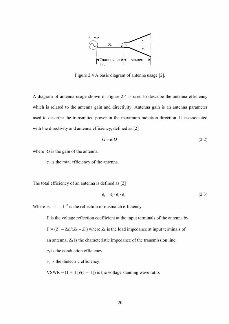
Figure 2.4 A basic diagram of antenna usage [2].
A diagram of antenna usage shown in Figure 2.4 is used to describe the antenna efficiency
which is related to the antenna gain and directivity. Antenna gain is an antenna parameter
used to describe the transmitted power in the maximum radiation direction. It is associated
with the directivity and antenna efficiency, defined as [2]
0G e D (2.2)
where G is the gain of the antenna.
e0 is the total efficiency of the antenna.
The total efficiency of an antenna is defined as [2]
0 r c de e e e (2.3)
Where er = 1 – ||2 is the reflection or mismatch efficiency.
is the voltage reflection coefficient at the input terminals of the antenna by
= (ZL – Z0)/(ZL – Z0) where ZL is the load impedance at input terminals of
an antenna, Z0 is the characteristic impedance of the transmission line.
ec is the conduction efficiency.
ed is the dielectric efficiency.
VSWR = (1 + ||)/(1 – ||) is the voltage standing wave ratio.
21
Essential background for antennas presented in this thesis is described in Section 2.1.2 for
dipole antennas and Section 2.1.3 for waveguide aperture antenna.
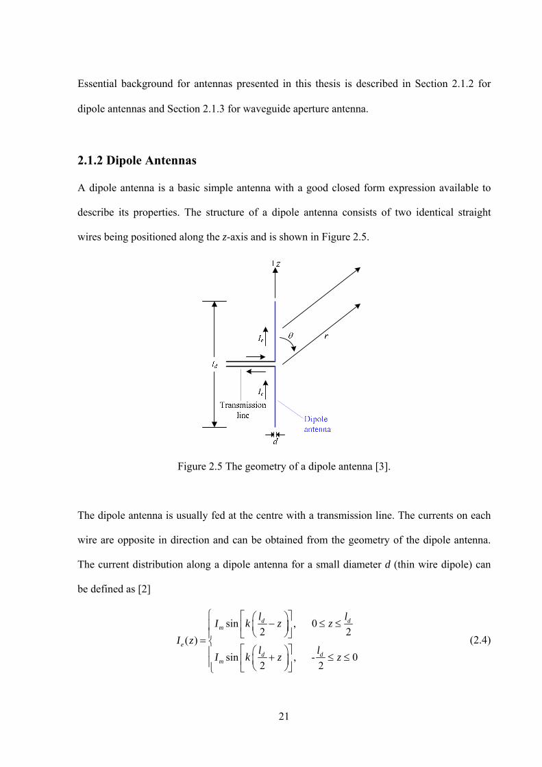
2.1.2 Dipole Antennas
A dipole antenna is a basic simple antenna with a good closed form expression available to
describe its properties. The structure of a dipole antenna consists of two identical straight
wires being positioned along the z-axis and is shown in Figure 2.5.
Figure 2.5 The geometry of a dipole antenna [3].
The dipole antenna is usually fed at the centre with a transmission line. The currents on each
wire are opposite in direction and can be obtained from the geometry of the dipole antenna.
The current distribution along a dipole antenna for a small diameter d (thin wire dipole) can
be defined as [2]
sin , 02 2
( )
sin , - 02 2
d dm
e
d dm
l lI k z z
I zl l
I k z z
(2.4)
22
where Ie is the current distribution along a thin wire dipole antenna.
Im is the maximum current magnitude.
k = 2/ is the propagation constant.
ld is the total dipole length.
The radiation pattern of the dipole antenna can be obtained from the line integral of the
current along the z-axis, given by [3]
/ 2 cos
/ 2sin sin
4
d
d
jkrl jkz
z el
eE j A j I z e dz
r
(2.5)
EH
(2.6)
where E is the electric field in the far field.
H is the magnetic field in the far field.
zA is the potential vector of the current along z-axis.
2 f is the radian frequency (rad/s).
is the permeability (H/m).
0
0
376.73 120
is the intrinsic impedance of free-space (ohms)
Substituting the current equation from (2.4) to (2.5) gives
0 cos
/ 2
/ 2 cos
0
sin sin4 2
sin (2.7)2
d
d
jkrjkzd
ml
l jkzdm
leE j I k z e dz
r
lI k z e dz
23
Solving the integral equation (2.7) gives
cos / 2 cos cos / 2
2 sin
jkrd dm
kl klI eE j
r
(2.8)
The magnetic field can be obtained as
cos / 2 cos cos / 2
2 sin
jkrd dm
kl klE I eH j
r
(2.9)
The current distribution and the normalised radiation pattern (E-field) for different dipole
lengths dl are obtained using equations (2.4) and (2.8), and shown in Table 2.1.
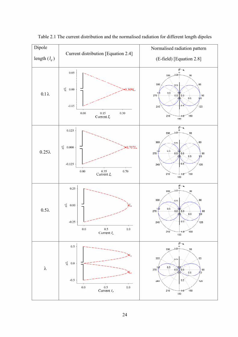
24
Table 2.1 The current distribution and the normalised radiation for different length dipoles
Dipole
length ( dl ) Current distribution [Equation 2.4]
Normalised radiation pattern
(E-field) [Equation 2.8]
25
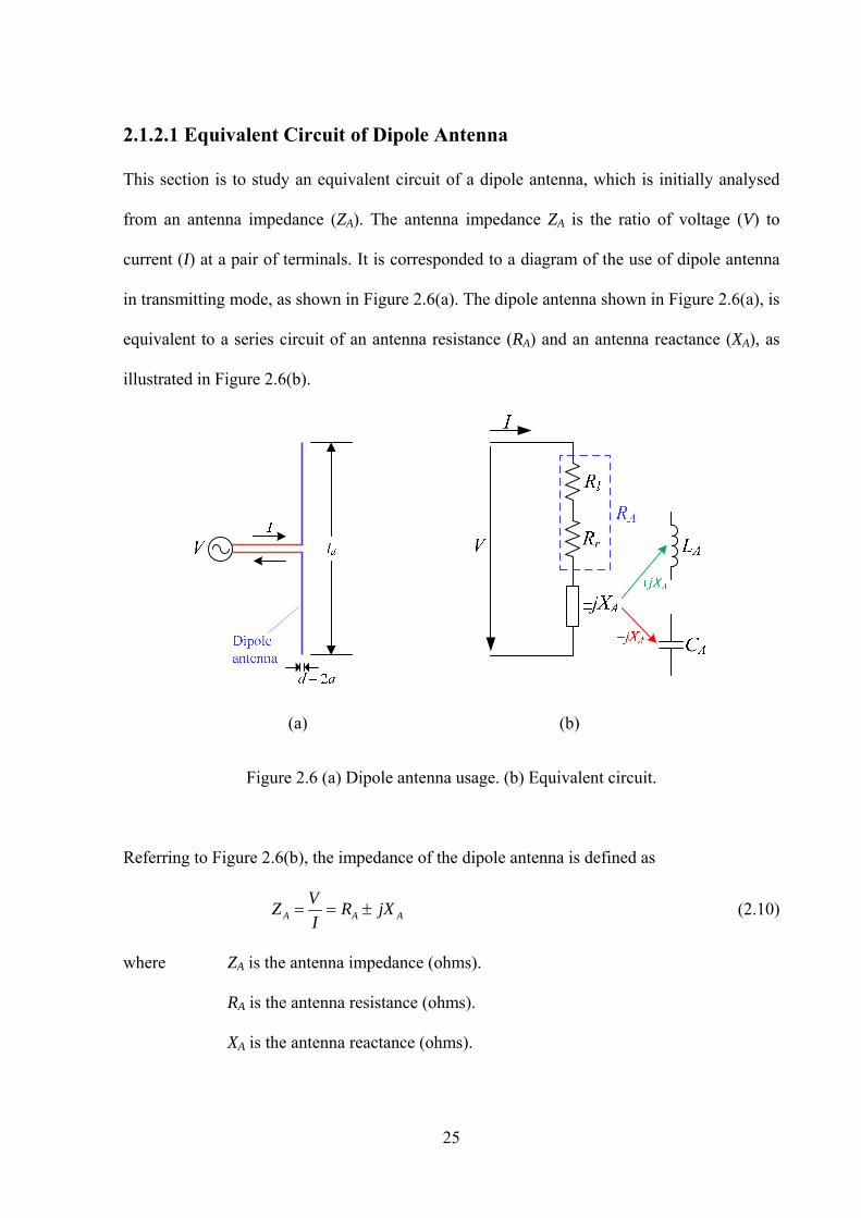
2.1.2.1 Equivalent Circuit of Dipole Antenna
This section is to study an equivalent circuit of a dipole antenna, which is initially analysed
from an antenna impedance (ZA). The antenna impedance ZA is the ratio of voltage (V) to
current (I) at a pair of terminals. It is corresponded to a diagram of the use of dipole antenna
in transmitting mode, as shown in Figure 2.6(a). The dipole antenna shown in Figure 2.6(a), is
equivalent to a series circuit of an antenna resistance (RA) and an antenna reactance (XA), as
illustrated in Figure 2.6(b).
(a) (b)
Figure 2.6 (a) Dipole antenna usage. (b) Equivalent circuit.
Referring to Figure 2.6(b), the impedance of the dipole antenna is defined as
A A A
VZ R jX
I (2.10)
where ZA is the antenna impedance (ohms).
RA is the antenna resistance (ohms).
XA is the antenna reactance (ohms).
26
For the resistive part of ZA, it represents RA by
RA = Rr + Rl (2.11)
where Rr is the radiation resistance (ohms).
Rl is the loss resistance (ohms).
For the reactive part of ZA, it represents XA, which can be a positive or a negative value. For
positive XA, it is equivalent to an antenna inductance (LA). For negative XA, it is equivalent to
an antenna capacitance (CA).
The equations used to calculate Rr and XA element values for finite length dipoles are derived
using the induced EMF method, given by [2]
1( ) ln sin 2 2
2 21
cos ln / 2 2 (2.12)2
r d d i d d i d i d
d d i d i d
R l C kl C kl kl S kl S kl
kl C kl C kl C kl
and
2
( ) 2 cos 2 24
2 sin 2 2 (2.13)
A d i d d i d i d
d i d i d id
X l S kl kl S kl S kl
kakl C kl C kl C
l
where ld is the length of the dipole antenna, a is the wire radius, k is the propagation constant
(k = 2/0), C = 0.5772 (Euler’s constant) and Ci(x) and Si(x) are the cosine and sine integrals
and given by
cosx
i
yC x dy
y (2.14)
0
sinx
i
yS x dy
y (2.15)
27
An example of Rr and XA calculation using equations (2.12) and (2.15) for a half-wavelength
(0.5) lossless dipole antenna (Rl = 0 ), the results shows that Rr is 73 ohms and XA is 42.5
ohms, which corresponded to the antenna theory.
The loss resistance Rl of wire dipole antenna represents the conductor loss and is considered
in a case of lossy dipole. Rl is calculated based on the current distribution, given by [3]
For a uniform current distribution,
0
4d
l
l fR
a
(2.16)
For a triangular current distribution,
0
6d
l
l fR
a
(2.17)
where a is the wire radius of dipole antenna.
f is the frequency (Hz).
0 is the permeability of free-space (4 x10⁻⁷ H/m).
is the conductivity of the metal (S/m).
For example, a loss resistance Rl of an half wave length dipole antenna made from the copper
( = 5.7x10⁷ S/m), wire radius a is 3x10⁻⁴. The Rl is calculated at f of 100 MHz using
equation (2.16) that is equal to 0.349 ohms. For equation (2.17), it is used to calculate Rl for a
short dipole antenna (ld << ).
28
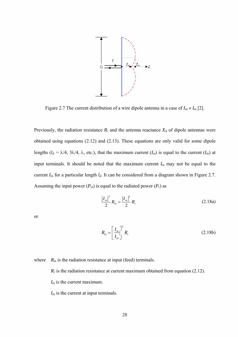
Figure 2.7 The current distribution of a wire dipole antenna in a case of Iin Im [2].
Previously, the radiation resistance Rr and the antenna reactance XA of dipole antennas were
obtained using equations (2.12) and (2.13). These equations are only valid for some dipole
lengths (ld = /4, 3/4, , etc.), that the maximum current (Im) is equal to the current (Iin) at
input terminals. It should be noted that the maximum current Im may not be equal to the
current Iin for a particular length ld. It can be considered from a diagram shown in Figure 2.7.
Assuming the input power (Pin) is equal to the radiated power (Pr) as
2 2
2 2in m
in r
I IR R (2.18a)
or
2
min r
in
IR R
I
(2.18b)
where Rin is the radiation resistance at input (feed) terminals.
Rr is the radiation resistance at current maximum obtained from equation (2.12).
Im is the current maximum.
Iin is the current at input terminals.
29
Referring to Figure 2.7, the current Iin is related to the maximum current Im for a length ld and
is given by [2]
sin2
din m
klI I
(2.19)
Substituting equations from (2.20) to (2.19), thus equation (2.19) can be written as
2sin2
rin
d
RR
kl
(2.20)
Also the antenna reactance (Xin) at input terminals of dipole antenna can be written as [2]
2sin2
Ain
d
XX
kl
(2.21)
Substituting equations from (2.12) to (2.21) and from (2.13) to (2.22) thus,
2
1( ) ln sin 2 2
22 sin
2
1 cos ln / 2 2 (2.22)
2
in d d i d d i d i dd
d d i d i d
R l C kl C kl kl S kl S klkl
kl C kl C kl C kl
and
2
2
( ) 2 cos 2 24 sin
2
2 sin 2 2 (2.23)
in d i d d i d i dd
d i d i d id
X l S kl kl S kl S klkl
kakl C kl C kl C
l
It is concluded that the input impedance (Zin) of a lossless dipole antenna is
inin in in
in
VZ R jX
I (2.24)
30
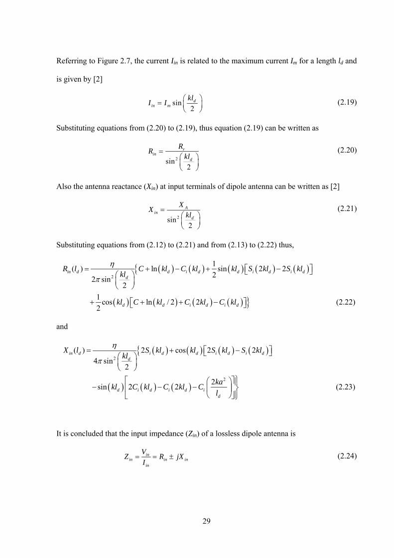
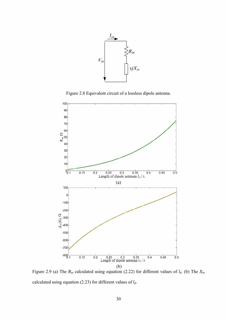
Figure 2.8 Equivalent circuit of a lossless dipole antenna.
(a)
(b)
Figure 2.9 (a) The Rin calculated using equation (2.22) for different values of ld. (b) The Xin
calculated using equation (2.23) for different values of ld.
31
It is represented as an equivalent circuit shown in Figure 2.8. The equivalent circuit of lossless
dipole will be used to define its quality factor that is a parameter in order to design a resonator
using dipole antenna in Chapter3. Figure 2.9 shows Rin and Xin calculated using equations
(2.23) and (2.24) for the length ld between 0.1 and 0.5. These Rin and Xin calculation will
then be utilised to calculate the quality factor (Q) of dipole antenna in Section 2.1.2.2.
2.1.2.2 Quality Factor of Dipole Antenna
The equivalent circuit of dipole antenna was analysed for different antenna lengths, as
described in Section 2.1.2.1. An antenna element can also be described as a resonator in terms
of the quality factor (Q). In this thesis, the dipole antenna will be initially studied and
designed for a lossless dipole (Rl = 0 ). This is because it is a simple way to determine its
quality factor, which is only related to the radiation or is named the radiation quality factor
Qr. The Qr can be obtained from the equivalent circuit of a lossless dipole, which is analysed
at the input. As mentioned in Section 2.1.2.1, a lossless dipole was equivalent to a Rin and Xin
series circuit. In this case, Qr of a lossless dipole can be calculated using the values of Rin and
Xin considering at f0, given by [4]
000
00 02
ininr
in
X fdX ffQ f
R f df f
(2.25)
where f0 is the centre frequency (Hz), Rin(f0) is the radiation resistance at the centre frequency
(), Xin(f0) is the antenna reactance at the centre frequency (), 0indX f
dfis the derivative of
Xin at the centre frequency and can also be defined as
32
0 0 0
2in in indX f X f f X f f
df f
and f is a small change in f
The value of f must be small to improve the accuracy of the calculation of Qr. The value
selected is about 1% of the bandwidth or 0.01 for this calculation.
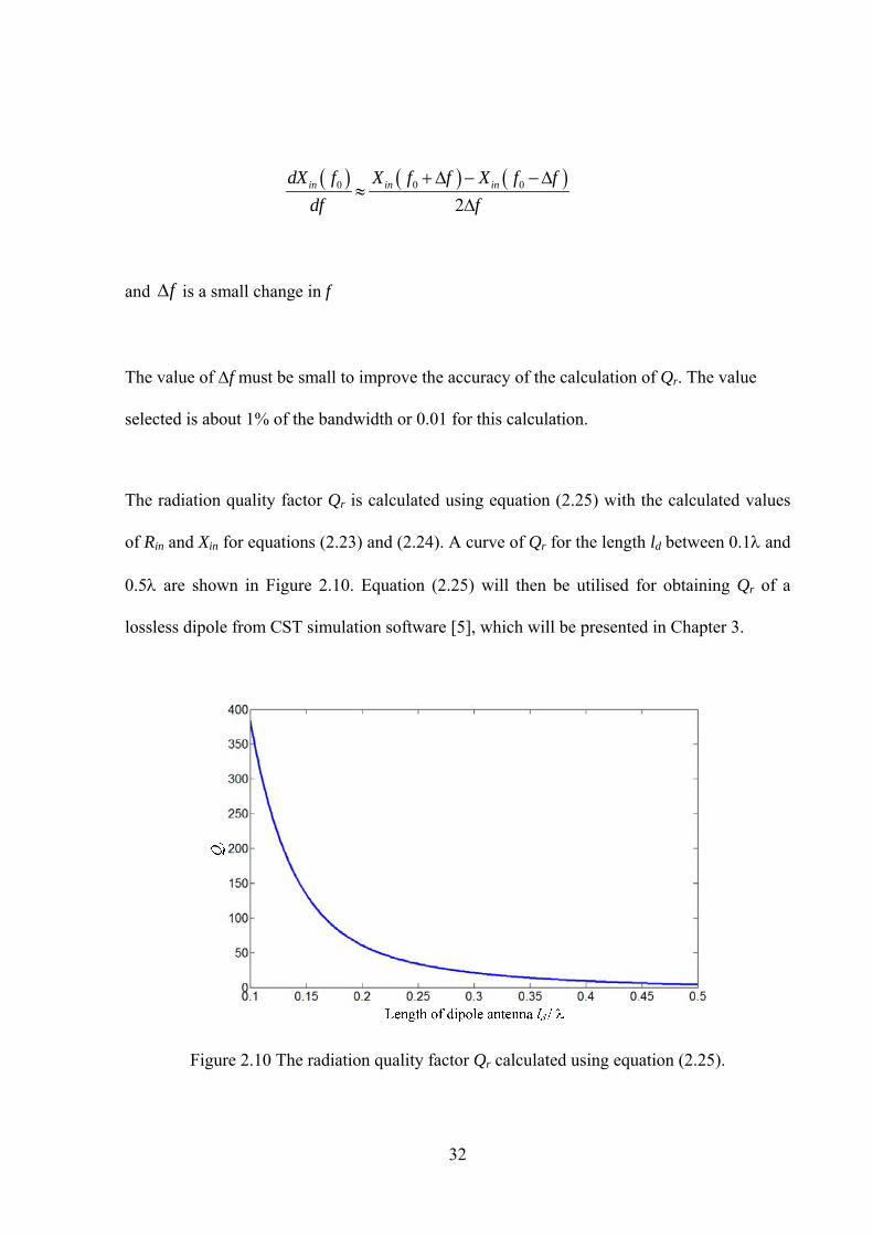
The radiation quality factor Qr is calculated using equation (2.25) with the calculated values
of Rin and Xin for equations (2.23) and (2.24). A curve of Qr for the length ld between 0.1 and
0.5 are shown in Figure 2.10. Equation (2.25) will then be utilised for obtaining Qr of a
lossless dipole from CST simulation software [5], which will be presented in Chapter 3.
Figure 2.10 The radiation quality factor Qr calculated using equation (2.25).

33
2.1.3 Waveguide Aperture Antennas
A waveguide aperture antenna is a simple antenna structure and is usually designed with an
opening at the end of a rectangular waveguide. The aperture area of the waveguide is used to
radiate the electromagnetic wave. Figure 2.11 shows the structure of the waveguide antenna
and the distribution of the E and H fields inside of the waveguide for the dominant TE10
mode.
Figure 2.11 The geometry of an open-ended waveguide antenna.
For the open-ended waveguide, the radiated power does not use the full physical aperture (Ap)
due to E-fields at the sidewall that becomes zero for TE10 propagation mode. Thus, the
effective area Ae of the aperture is less than the physical aperture Ap and corresponds to the
aperture efficiency ap of the antenna as given by [2]
eap
p
A
A (2.26)
The radiated power of the aperture antenna can be obtained by integrating the average
Poynting vector Wav and is given by [2]
2
0
4rad av
S
EP W dS ab
(2.27)
The maximum radiation intensity Umax at = 0o is given by [2]
34
220
max 2
8
4
EabU
(2.28)
The maximum directivity D0 of the aperture antenna is obtained using equation [2]:
max0 2 2 2 2 2
4 8 4 4 4 40.81 0.81 p em
rad
UD ab ab A A
P
(2.29)
where Ap = a x b is the physical aperture for the open-ended waveguide antenna.
Aem = apAp = 0.81Ap is the maximum effective aperture for the open-ended
waveguide antenna.
Thus, the aperture efficiency ap for the waveguide aperture antenna is equal to 0.81, which
indicates 81% efficiency of the physical aperture Ap can be utilised for radiating EM energy.
It is noted that the equation (2.29) is only valid for the aperture mounted on the infinite
ground plane.
2.2 Microwave Filter Theory
2.2.1 Overview of Microwave Filters
As this project is about combining antennas and filters we now move on the filter theory. A
microwave filter is a two-port passive component utilised for selecting a required frequency
and rejecting an unwanted frequency in the microwave frequency range (300 MHz–300 GHz)
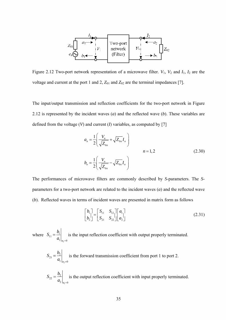
[6]. The microwave filter is represented by a two-port network [7], as shown in Figure 2.12.
35
Figure 2.12 Two-port network representation of a microwave filter. V1, V2 and I1, I2 are the
voltage and current at the port 1 and 2, Z01 and Z02 are the terminal impedances [7].
The input/output transmission and reflection coefficients for the two-port network in Figure
2.12 is represented by the incident waves (a) and the reflected wave (b). These variables are
defined from the voltage (V) and current (I) variables, as computed by [7]
0
0
0
0
1
2
1, 2
1
2
nn n n
n
nn n n
n
Va Z I
Z
n
Vb Z I
Z
(2.30)
The performances of microwave filters are commonly described by S-parameters. The S-
parameters for a two-port network are related to the incident waves (a) and the reflected wave
(b). Reflected waves in terms of incident waves are presented in matrix form as follows
1 11 12 1
2 21 22 2
b S S a
b S S a
(2.31)
where 2
111
1 0a
bS
a
is the input reflection coefficient with output properly terminated.
2
221
1 0a
bS
a
is the forward transmission coefficient from port 1 to port 2.
1
222
2 0a
bS
a
is the output reflection coefficient with input properly terminated.

36
1
112
2 0a
bS
a
is the reverse transmission coefficient from port 2 to port 1.
The characteristics of filters are shown by the transmission loss LA and the return loss LR
which are obtained from the magnitude of S-parameters for the two-port network in decibels,
as follows
10 2120logAL S dB (2.32a)
10 1120logRL S dB (2.32b)
The transmission and return losses are assumed to have positive values. The relation between
the transmission loss LA and return loss LR for a lossless network only are given by [7]
/101010log 1 10 RL
AL dB (2.33a)
/101010log 1 10 AL
RL dB (2.33b)
(a)
g0
g1
g2
g3
gn gn+1
(n even)
gn
gn+1
(n odd)
or
(b)
Figure 2.13 Lowpass prototype filters for all-pole filters with (a) A ladder circuit beginning
with a shunt element and (b) A ladder circuit beginning with a series element [7].
37
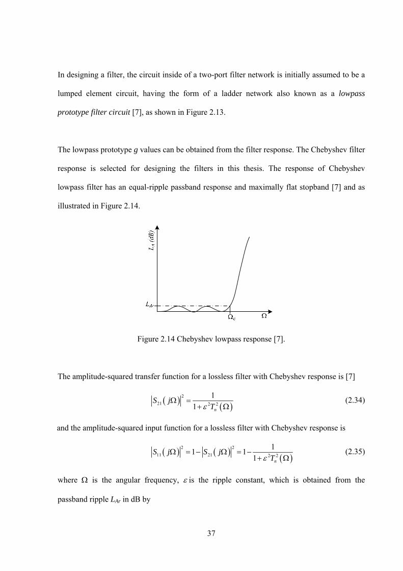
In designing a filter, the circuit inside of a two-port filter network is initially assumed to be a
lumped element circuit, having the form of a ladder network also known as a lowpass
prototype filter circuit [7], as shown in Figure 2.13.
The lowpass prototype g values can be obtained from the filter response. The Chebyshev filter
response is selected for designing the filters in this thesis. The response of Chebyshev
lowpass filter has an equal-ripple passband response and maximally flat stopband [7] and as
illustrated in Figure 2.14.
Figure 2.14 Chebyshev lowpass response [7].
The amplitude-squared transfer function for a lossless filter with Chebyshev response is [7]
2
21 2 2
1
1 n
S jT
(2.34)
and the amplitude-squared input function for a lossless filter with Chebyshev response is
2 2
11 21 2 2
11 1
1 n
S j S jT
(2.35)
where is the angular frequency, is the ripple constant, which is obtained from the
passband ripple LAr in dB by
38
1010 1ArL
(2.36)
A Chebyshev function Tn() of the nth order filter can be defined as [7]
1
1
cos cos 1
cosh cosh 1n
nT
n
(2.37)
The g values for a lowpass prototype filter having the Chebyshev response the passband
ripple is LAr in dB and the cutoff frequency c = 1 can be calculated using equations below
[7]: In these equations
0 1.0g
1
2sin
2g
n
1 2 2
2 1 2 34sin sin
2 21 for = 2, 3,
1sin
ii
i i
n ng i n
g i
n
(2.38)
1 2
1.0 for odd
coth for even4
n
n
gn
where
ln coth17.37
ArL
sinh2n
Using these equations a low pass prototype filters can be calculated and the g element values
shown in Figure 2.13 calculated.
39
2.2.2 Microwave Resonators
Microwave resonators are microwave devices utilised in microwave coupled resonator filters.
Examples are microstrip resonators, cavity resonators, dielectric resonators, etc.. The
microwave resonator can be modeled as a similar circuit to a lumped-element resonator (i.e. a
series or parallel resonant circuit). Figure 2.15 shows the equivalent circuit of several
microwave resonators. A lossless resonator is an ideal resonator with no loss, i.e. R = 0 in
Figure 2.15(a) for a series circuit and Figure 2.15(b) for a parallel circuit.
(a) (b)
(c) (d)
Figure 2.15 The resonant circuits represented as microwave resonators. (a) Series lossless
resonant circuit. (b) Parallel lossless resonant circuit. (c) Series lossy resonant circuit.
(d) Parallel lossy resonant circuit.
40
For lossy resonators, the losses in the resonator are conventionally represented by the
resistance (R) in the resonant circuit of Figure 2.15(c) or the conductance (G) in the resonant
circuit of Figure 2.15(d). The unloaded quality factor (Qu) is a parameter used to describe the
losses of a resonant circuit. For example, a low loss implies a high Qu, whereas a high loss
implies a low Qu. For the series lossy resonant circuit, the unloaded quality factor Qu is
defined by [7]
u
LQ
R
(2.39)
For the parallel lossy resonant circuit, The unloaded quality factor Qu is defined by [7]
u
CQ
G
(2.40)
In principle, the general definition of the unloaded quality factor Qu is [7]
Time-average energy stored in resonator
Average power lost in resonatoruQ (2.41)
The losses in the resonator are usually associated with the conductors, dielectrics in the
resonator and radiation from the resonator. Thus, the total unloaded quality factor Qu can be
determined by including these losses together [7]
1 1 1 1
u c d rQ Q Q Q (2.42)
where Qc is the conductor quality factor, Qd is the dielectric quality factor and Qr is the
radiation quality factor.
41
In filter design, the passband response of the filters may be distorted due to the losses in the
resonators of the filter circuits. The value of unloaded quality factor Qu can be used to
calculate the insertion loss in the bandpass filter design using the resonators with finite Qu,
given by [7]
C0
1
4.343 (dB)n
A ii ui
L gFBW Q
(2.43)
where 0AL is the increase of passband insertion loss in dB, FBW is the fractional bandwidth
(FBW = (f2 – f1)/2), f2 – f1 is the passband bandwidth, C is the cut-off frequency (C = 1), gi
is the g values for i elements obtained from the filter response and Qui is the unloaded quality
factor for i resonator.
2.2.3 Rectangular Waveguide Cavity Resonator
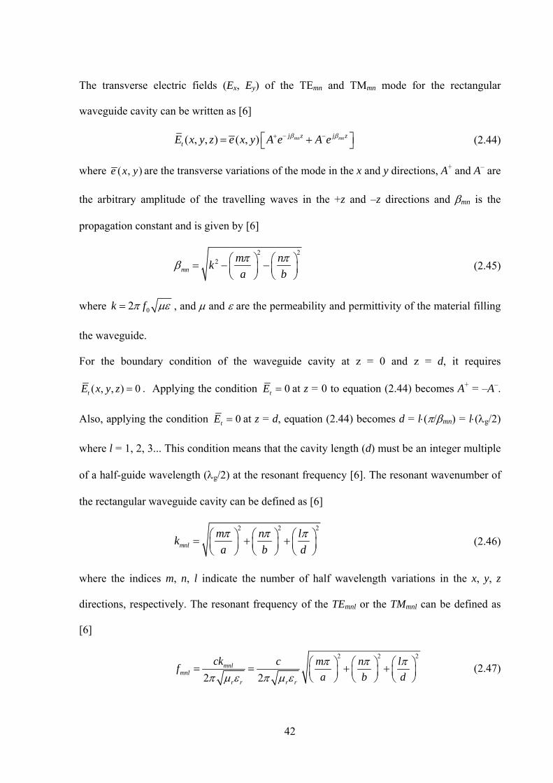
A rectangular waveguide cavity resonator can be made from a section of a rectangular
waveguide that is terminated at both ends with conducting plates. Figure 2.16 shows the
geometry of a rectangular waveguide cavity where a is the width, b is the height and d is the
length.
Figure 2.16 A rectangular waveguide cavity [6].
42
The transverse electric fields (Ex, Ey) of the TEmn and TMmn mode for the rectangular
waveguide cavity can be written as [6]
( , , ) ( , ) mn mnj z j ztE x y z e x y A e A e (2.44)
where ( , )e x y are the transverse variations of the mode in the x and y directions, A+ and A– are
the arbitrary amplitude of the travelling waves in the +z and –z directions and mn is the
propagation constant and is given by [6]
2 22
mn
m nk
a b
(2.45)
where 02k f , and and are the permeability and permittivity of the material filling
the waveguide.
For the boundary condition of the waveguide cavity at z = 0 and z = d, it requires
( , , ) 0tE x y z . Applying the condition 0tE at z = 0 to equation (2.44) becomes A+ = –A–.
Also, applying the condition 0tE at z = d, equation (2.44) becomes d = l(/mn) = l(g/2)
where l = 1, 2, 3... This condition means that the cavity length (d) must be an integer multiple
of a half-guide wavelength (g/2) at the resonant frequency [6]. The resonant wavenumber of
the rectangular waveguide cavity can be defined as [6]
2 2 2
mnl
m n lk
a b d
(2.46)
where the indices m, n, l indicate the number of half wavelength variations in the x, y, z
directions, respectively. The resonant frequency of the TEmnl or the TMmnl can be defined as
[6]
2 2 2
2 2mnl
mnl
r r r r
ck c m n lf
a b d
(2.47)
43
where c = 3 x 10⁸ m/s is the light speed, and r and r are the relative permeability and
permittivity of the material filling the waveguide. In the case of b < a < d, the mode with the
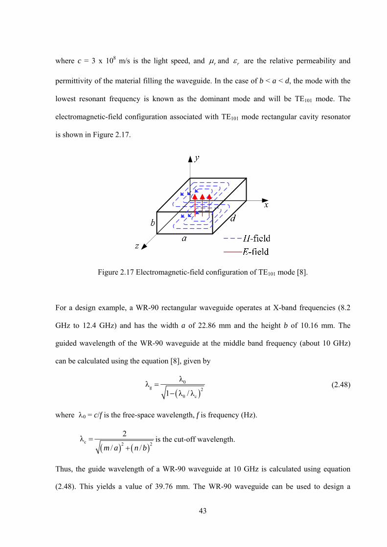
lowest resonant frequency is known as the dominant mode and will be TE101 mode. The
electromagnetic-field configuration associated with TE101 mode rectangular cavity resonator
is shown in Figure 2.17.
Figure 2.17 Electromagnetic-field configuration of TE101 mode [8].
For a design example, a WR-90 rectangular waveguide operates at X-band frequencies (8.2
GHz to 12.4 GHz) and has the width a of 22.86 mm and the height b of 10.16 mm. The
guided wavelength of the WR-90 waveguide at the middle band frequency (about 10 GHz)
can be calculated using the equation [8], given by
0
g 2
0 c
λλ
1 λ / λ
(2.48)
where 0 = c/f is the free-space wavelength, f is frequency (Hz).
c 2 2
2λ
/ /m a n b
is the cut-off wavelength.
Thus, the guide wavelength of a WR-90 waveguide at 10 GHz is calculated using equation
(2.48). This yields a value of 39.76 mm. The WR-90 waveguide can be used to design a
44
cavity resonator terminated at both ends with conducting plates. The resonator is half a guide
wavelength long. Using equation (2.47), and assuming that the inside of cavity is filled with
air (i.e. 1r r ), the calculated resonant frequency (f101) of the TE101 mode is 10 GHz.
2.2.4 Coupled Resonator Filters
Microwave bandpass filter is usually designed based on coupled resonator circuit. The filter
can be simply designed by combining all resonators using coupling theory, as described in
[7].
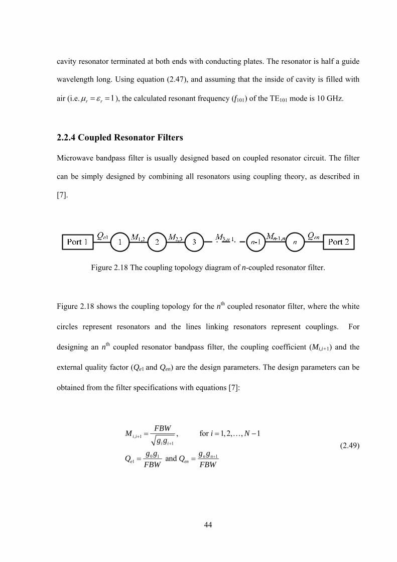
Figure 2.18 The coupling topology diagram of n-coupled resonator filter.
Figure 2.18 shows the coupling topology for the nth coupled resonator filter, where the white
circles represent resonators and the lines linking resonators represent couplings. For
designing an nth coupled resonator bandpass filter, the coupling coefficient (Mi,i+1) and the
external quality factor (Qe1 and Qen) are the design parameters. The design parameters can be
obtained from the filter specifications with equations [7]:
, 1
1
0 1 11
, for 1,2, , 1
and
i i
i i
n ne en
FBWM i N
g g
g g g gQ Q
FBW FBW
(2.49)
45
In the normalised form,
, 1, 1
1
1 1 0 1 1
1, for 1,2, , 1
and
i ii i
i i
e e en en n n
Mm i N
FBW g g
q FBW Q g g q FBW Q g g
(2.50)
where Mi,i+1 is the coupling coefficient between adjacent resonators.
Qe1 and Qen are the external quality factors of the input and output resonators.
2 1
0
f fFBW
f
is the fractional bandwidth.
f2 – f1 is the design bandwidth.
f0 is the centre frequency.
mi,i+1 is the normalised coupling coefficient between adjacent resonators.
qe1 and qen are the normalised external quality factors of the input and output
resonators.
g is the g value obtained from the filter response (e.g. Chebyshev filter response from
equation (2.38)).
The normalised design parameters will then be utilised with the coupling matrix to calculate
the filter response corresponding to filter specifications.
2.2.5 Coupling Matrix for Coupled Resonator Filters
The coupled resonator filters are conventionally designed using the coupling coefficient
(Mi,i+1) and the external quality factors (Qe1 and Qen), as described in the previous section. The
46
coupling matrix is a general technique for analysing the filter response of coupled resonator
filters based on the coupling coefficient and the external quality factor with couplings
potentially between any every pair of resonators. The coupling matrix is derived from the
coupled resonator circuits and can be applicable to design filters for different coupling
topologies. The calculated coupling values, from the coupling matrix, can then be utilised for
defining the physical dimensions for the filter structure. The coupling coefficient and the
external quality factor extraction technique are dependent on the filter structure and will be
described in the next chapters. This section derives the coupling matrix equations for coupled
resonator filters with the lossy and lossless resonators. Here the lossy resonators are assumed
in the filter circuit when deriving the coupling matrix equation in the case of filter circuits
with finite Qu. The n-coupled resonator filter circuits with finite Qu for the magnetic coupling
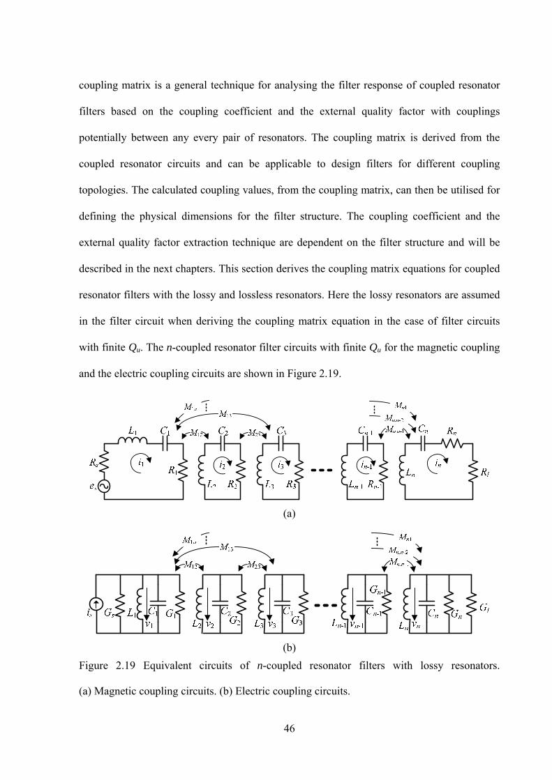
and the electric coupling circuits are shown in Figure 2.19.
(a)
(b)
Figure 2.19 Equivalent circuits of n-coupled resonator filters with lossy resonators.
(a) Magnetic coupling circuits. (b) Electric coupling circuits.
47
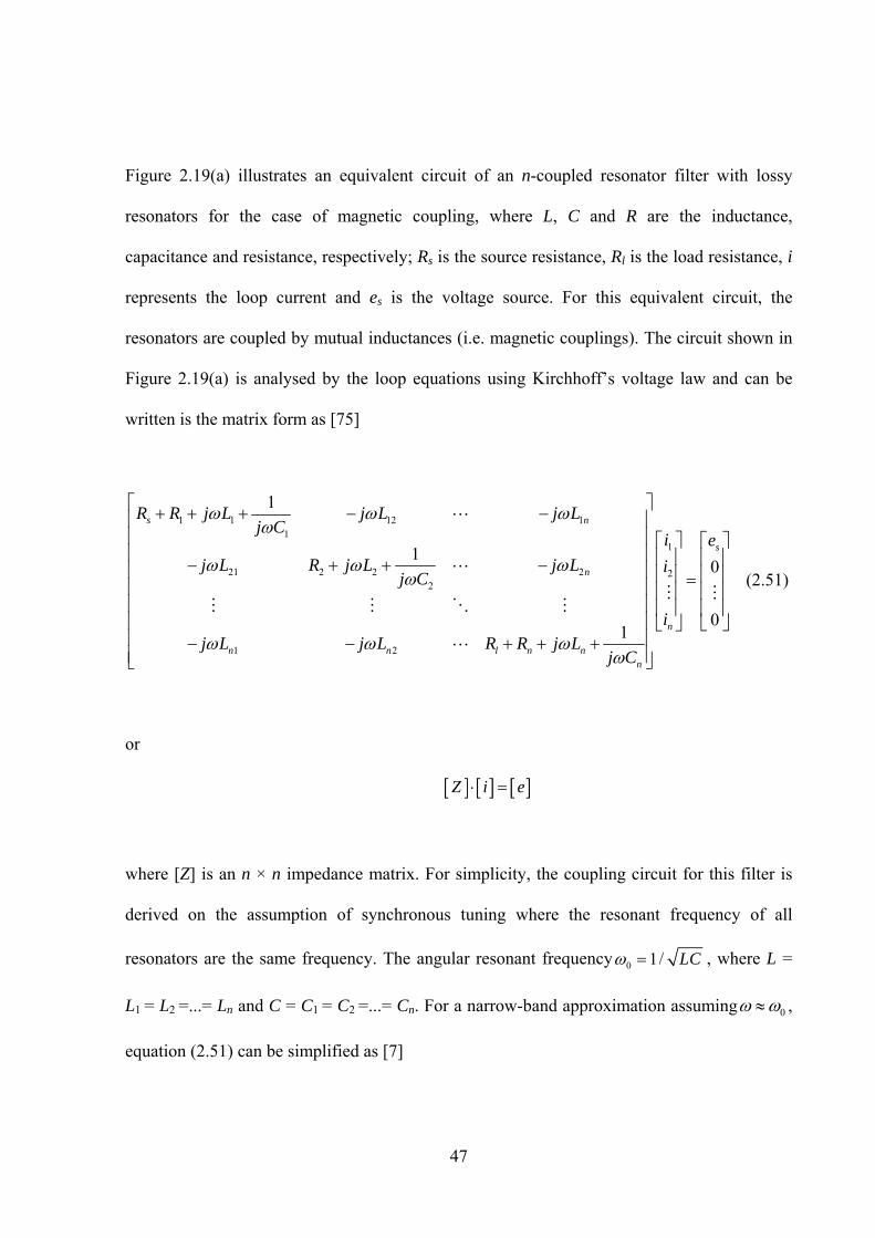
Figure 2.19(a) illustrates an equivalent circuit of an n-coupled resonator filter with lossy
resonators for the case of magnetic coupling, where L, C and R are the inductance,
capacitance and resistance, respectively; Rs is the source resistance, Rl is the load resistance, i
represents the loop current and es is the voltage source. For this equivalent circuit, the
resonators are coupled by mutual inductances (i.e. magnetic couplings). The circuit shown in
Figure 2.19(a) is analysed by the loop equations using Kirchhoff’s voltage law and can be
written is the matrix form as [75]
1 1 12 11
1
21 2 2 2 22
1 2
1
10
01
s n
s
n
n
n n l n nn
R R j L j L j Lj C
i e
j L R j L j L ij C
ij L j L R R j L
j C
(2.51)
or
Z i e
where [Z] is an n × n impedance matrix. For simplicity, the coupling circuit for this filter is
derived on the assumption of synchronous tuning where the resonant frequency of all
resonators are the same frequency. The angular resonant frequency 0 1/ LC , where L =
L1 = L2 =...= Ln and C = C1 = C2 =...= Cn. For a narrow-band approximation assuming 0 ,
equation (2.51) can be simplified as [7]
48
12 11 1
21 22
1 2
1 1
1
1 1
ne u
nu
n nen un
p jm jmq q
jm p jmqZ
jm jm pq q
(2.52)
where Z is the normalised impedance matrix.
0
0
1p j
FBW
is the complex frequency variable.
1 1 e eq FBW Q is the normalised external quality factor of input resonator.
01e
s
LQ
R
is the external quality factor of input resonator.
en enq FBW Q is the normalised external quality factor of output resonator.
0en
l
LQ
R
is the external quality factor of output resonator.
(for 1,2, , )ui uiq FBW Q i n is the normalised unloaded quality factor
of resonator i.
0 (for 1, 2, , )uii
LQ i n
R
is the unloaded quality factor of resonator i.
ijij
Mm
FBW is the normalised coupling coefficient of resonator i and j.
ijij
LM
L is the coupling coefficient of resonator i and j.
All resonators of the circuit of Figure 2.19(a) may have different resonant frequencies in the
case of asynchronously tuned coupled-resonator circuits [7]. The normalised self-coupling
49
coefficient mii accounts for asynchronous tuning and is related to the self-resonant frequency
of each resonator. The mii can be added into the diagonal entries in Z , for asynchronous
tuning as [7]
11 12 11 1
21 22 22
1 2
1 1
1
1 1
ne u
nu
n n nnen un
p jm jm jmq q
jm p jm jmqZ
jm jm p jmq q
(2.53)
(a)
(b)
Figure 2.20 Network representation of two-port circuit in (a) Figure 2.19(a) and (b) Figure
2.19 (b).
50
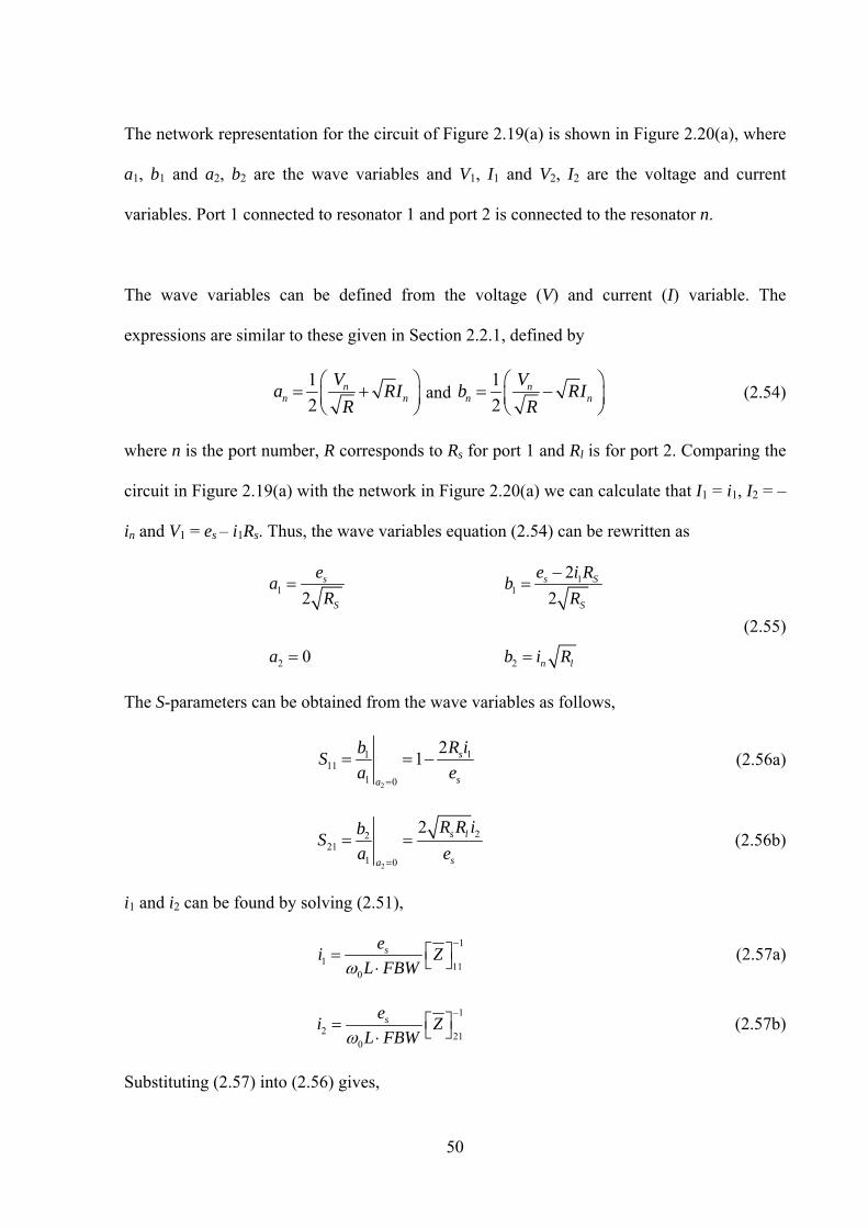
The network representation for the circuit of Figure 2.19(a) is shown in Figure 2.20(a), where
a1, b1 and a2, b2 are the wave variables and V1, I1 and V2, I2 are the voltage and current
variables. Port 1 connected to resonator 1 and port 2 is connected to the resonator n.
The wave variables can be defined from the voltage (V) and current (I) variable. The
expressions are similar to these given in Section 2.2.1, defined by
1
2n
n n
Va RI
R
and 1
2n
n n
Vb RI
R
(2.54)
where n is the port number, R corresponds to Rs for port 1 and Rl is for port 2. Comparing the
circuit in Figure 2.19(a) with the network in Figure 2.20(a) we can calculate that I1 = i1, I2 = –
in and V1 = es – i1Rs. Thus, the wave variables equation (2.54) can be rewritten as
11 1
2 2
2
2 2
0
s s S
S S
n l
e e i Ra b
R R
a b i R
(2.55)
The S-parameters can be obtained from the wave variables as follows,
2
1111
1 0
21 s
sa
R ibS
a e
(2.56a)
2
2221
1 0
2 s l
sa
R R ibS
a e
(2.56b)
i1 and i2 can be found by solving (2.51),
1
1 110
sei Z
L FBW
(2.57a)
1
2 210
sei Z
L FBW
(2.57b)
Substituting (2.57) into (2.56) gives,
51
1
11 110
21 sR
S ZL FBW
(2.58a)
1
21 210
2 s lR RS Z
L FBW
(2.58b)
Rewriting (2.58) in terms of the normalised external quality factors ( 1 0 /e sq L FBW R and
0 /en lq L FBW R ). Thus, S-parameters become,
1
11 111
21
e
S Zq
(2.59a)
1
2121
1
2
e en
S Zq q
(2.59b)
Similarly, the equivalent circuit of the resonators coupled by mutual capacitances (i.e. electric
couplings) shown in Figure 2.19(b) can be analysed by the node equation using Kirchhoff’s
current law. The normalised admittance matrix Y for the filter of Figure 2.19(b) can be
defined as
11 12 11 1
21 22 22
1 2
1 1
1
1 1
ne u
nu
n n nnen un
p jm jm jmq q
jm p jm jmqY
jm jm p jmq q
(2.60)
The S-parameters for the filter circuit in Figure 2.19(b) can be defined in a similar way to that
for the magnetic coupling circuit
1
11 111
21
e
S Yq
(2.61a)
52
1
211
1
12
ne en
S Yq q
(2.61b)
It can be concluded that the normalised impedance matrix Z and the normalised admittance
matrix Y are of the same form. Thus, the S-parameters for these coupling circuits may be
defined as
1
11 111
21
e
S Aq
(2.62a)
1
21 11
12
ne en
S Aq q
(2.62b)
where the matrix [A] is
1 111 12 1
21 22 22
1 2
1 10 0
1 0 01
0 0 0 1 0
0 0 11 1
0 0
e un
nu
n n nn
en un
q qm m m
m m mqA p j
m m m
q q
(2.63)
or A q p U j m
where [A] is the sum of three n x n matrices, [U] is the n x n identity matrix, [q] is an n x n
quality factor matrix, [m] is an n x n coupling matrix.
In a case of filters with lossless resonators, the coupling matrix equation is derived in a
similar way to that for filters with finite Qu by not considering the loss resistance in the all
resonators. Thus, the matrix [A] for the lossless filter is defined as [7]
53
1 11 12 1
21 22 2
1 2
10 0
1 0 0
0 0 0 0 1 0
1 0 0 10 0
e n
n
n n nn
en
q m m m
m m mA p j
m m m
q
(2.64)
The S-parameter equations for the lossless filter circuits are the same as the equations for the
filter with finite Qu (equations (2.62a) and (2.62b)).
2.3 Coupling Matrix for Antenna-Filters
Previously, the antenna and microwave filter theories have been presented and related to the
work in this thesis. Both theories will be used for the new design, involving antenna and filter
integration based on the coupled resonator filter theory [7]. The antenna theory will then be
applied to design the dipole antennas in Chapter 3 and 4, and waveguide aperture antennas in
Chapter 5. The antennas will then be designed to perform as resonators integrated into the
coupled resonator circuit. As a first step, we will follow the study of the coupled resonator
filter theory to design a conventional two-port bandpass filter using all the dipole antennas as
resonators presented in Chapter3. The principle of the work will then be used to design an
antenna-filter in which all resonators are dipole antennas with the second port replaced as the
radiation port. All the designs in this work are presented in Chapter 4 and are designed using
the coupling matrix synthesis. Figure 2.21(a) shows a topology of n-coupled resonator
antenna-filter; where the white circles represent resonators, the solid lines linking resonators
represent couplings and a dashed line with an arrow represents radiation from the antenna.
The coupling matrix equation for this topology can be derived in a similar way of to that
given in Section 2.2.5, considering the external output as the source of radiation (qen = qrn)

54
and assuming the antenna is lossless. The coupling matrix equation of the topology in Figure
2.21(a) is defined as
1 11 12 1
21 22 2
1 2
10 0
1 0 0
0 0 0 0 1 0
1 0 0 10 0
e n
n
n n nn
rn
q m jm jm
jm m jmA p j
jm jm m
q
(2.65)
or A q p U j m
where [A] is the sum of three n x n matrices, [U] is an n x n identity matrix, [q] is an n x n
quality factor matrix, [m] is an n x n matrix of coupling factors.
(a)
(b)
Figure 2.21 The coupling topology diagram of n-coupled resonator antenna-filter for (a) The
last resonator is the antenna (Chapter 5), (b) All resonators are antennas (Chapter 4).
Figure 2.21(b) shows the topology of an n-coupled resonator antenna-filter in which all
resonators are antennas, the white circles represent antennas. The coupling matrix equation
for this topology can be derived in a similar way to that shown in Section 2.2.5, assuming that
the antennas are lossless. The coupling matrix equation of the topology in Figure 2.21(b) is
defined as
55
1 111 12 1
21 22 22
1 2
1 10 0
1 0 01
0 0 0 1 0
0 0 11
0 0
e rn
nr
n n nn
rn
q qm jm jm
jm m jmqA p j
jm jm m
q
(2.66)
or A q p U j m
where [A] is the sum of three n x n matrices, [U] is the n x n identity matrix, [q] is an n x n
quality factor matrix, [m] is an n x n coupling matrix.
This is a one port component which is considered only the reflection coefficient S11. The
magnitude of S11, for this coupling matrix is given by
1
11 111
21
e
S Aq
(2.67)
The coupling matrix for equation (2.66) can be utilised to design the antenna-filter using the
dipole antennas which will be presented in Chapter 4. Also, the coupling matrix for equation
(2.65) can be utilised in the design of waveguide antenna-filters in Chapter 5.
2.4 CST Microwave Studio
High frequency (HF) components are usually designed and simulated using Electromagnetic
(EM) simulators in order to analyse their parameters such as S-parameters, radiation
patterns,..etc.. The EM simulator uses the Maxwell’s equation solver to analyse the modeled
structure depending on the boundary conditions. It also uses numerical methods in order to
56
obtain accurate results. The numerical methods consist of finite element method (FEM), finite
different time domain method (FDTD), method of moment (MOM) and integral equation
method (IEM). Each method is suitable for specific type of calculation. The main
requirements of users for the EM simulator are easy in use, fast simulation and high accurate
results. The structures of designed components presented in this thesis have been simulated
using CST Microwave studio software [5]. This section provides an overview of CST
software in Section 2.4.1 and a few instruction of CST usage.
2.4.1 CST Microwave Studio Overview
CST Microwave studio [5] is an EM commercial simulation software and can provide those
requirements of users. This software includes 3D solver, circuit simulator and optimiser. The
solvers in CST software package consist of a transient domain (TD) solver, frequency domain
(FD) solver, Eigenmode (EM) solver, Integral equation (IE) solver, Asymptotic (A) solver
and TLM solver. The work presented in this thesis is to design an antenna-filter which will be
simulated in the open boundary with add space using a solver in CST software package. Here
TD solver is a simulation tool for structures designed in the opened boundary using the finite
frequency domain (FDTD) method. This solver is suitable for use in this work and shows
good agreement between simulation and the measurement results.
2.4.2 Instruction for using CST Microwave Studio
Figure 2.22 shows a beginning of opened CST software usage. It shows a new project creator
which provides the supporting templates for user in order to set up the new project. It can be
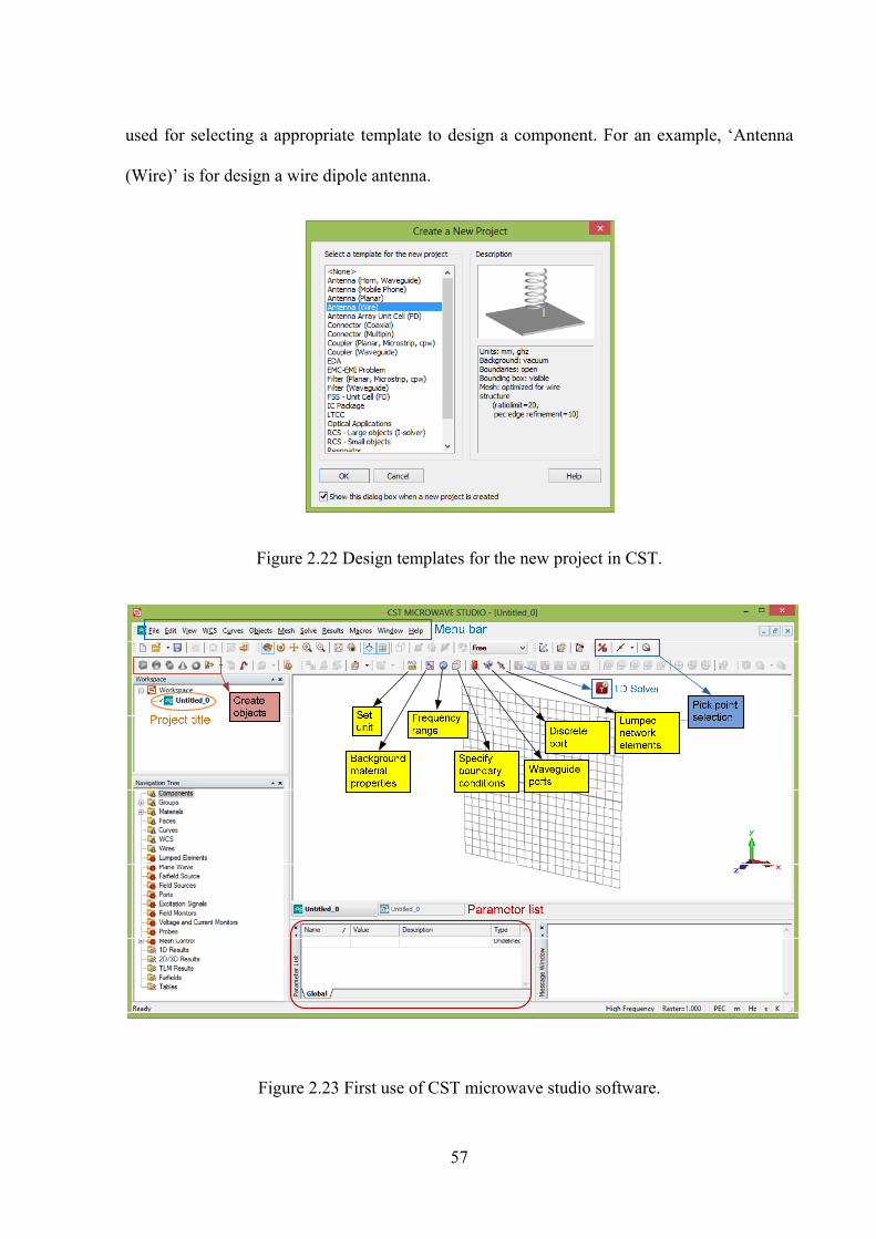
57
used for selecting a appropriate template to design a component. For an example, ‘Antenna
(Wire)’ is for design a wire dipole antenna.
Figure 2.22 Design templates for the new project in CST.
Figure 2.23 First use of CST microwave studio software.

58
After created the project, the CST microwave studio software will be displayed in Figure
2.23. In the CST software, there are many tools displayed as small icons. It is used for setting
up the design project. Here we will describe only the most tools shown in Figure 2.23 for
basic users. The tool box usage in CST microwave studio software will be described in step
by step as follows:
Figure 2.24 Unit setting menu.
Step 1, the units is firstly setting up in a design of component and is shown in Figure 2.24. It
can be set the required units that normally include the dimension, frequency, temperature and
time units.
Figure 2.25 Background property setting menu.
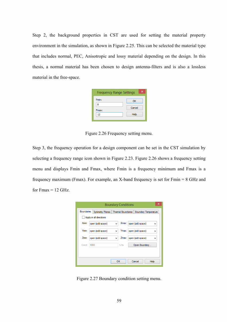
59
Step 2, the background properties in CST are used for setting the material property
environment in the simulation, as shown in Figure 2.25. This can be selected the material type
that includes normal, PEC, Anisotropic and lossy material depending on the design. In this
thesis, a normal material has been chosen to design antenna-filters and is also a lossless
material in the free-space.
Figure 2.26 Frequency setting menu.
Step 3, the frequency operation for a design component can be set in the CST simulation by
selecting a frequency range icon shown in Figure 2.23. Figure 2.26 shows a frequency setting
menu and displays Fmin and Fmax, where Fmin is a frequency minimum and Fmax is a
frequency maximum (Fmax). For example, an X-band frequency is set for Fmin = 8 GHz and
for Fmax = 12 GHz.
Figure 2.27 Boundary condition setting menu.
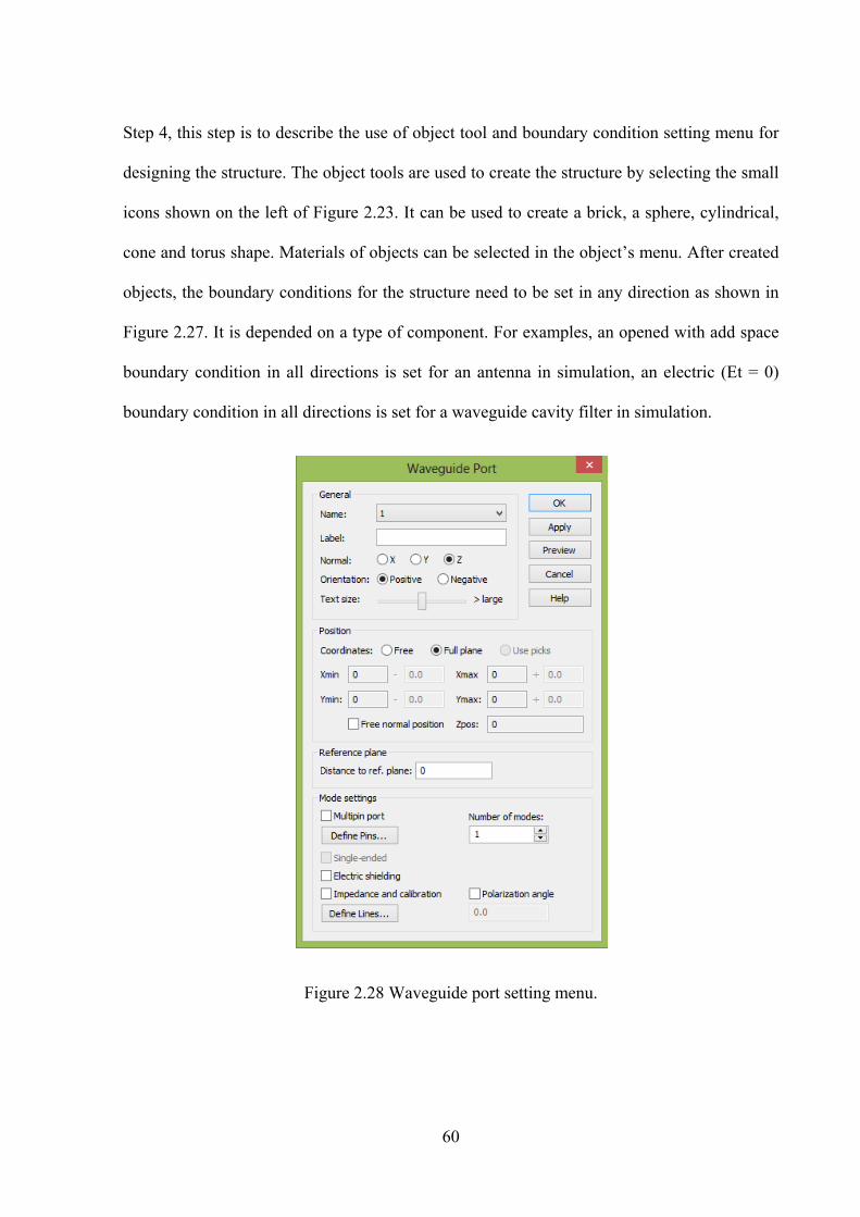
60
Step 4, this step is to describe the use of object tool and boundary condition setting menu for
designing the structure. The object tools are used to create the structure by selecting the small
icons shown on the left of Figure 2.23. It can be used to create a brick, a sphere, cylindrical,
cone and torus shape. Materials of objects can be selected in the object’s menu. After created
objects, the boundary conditions for the structure need to be set in any direction as shown in
Figure 2.27. It is depended on a type of component. For examples, an opened with add space
boundary condition in all directions is set for an antenna in simulation, an electric (Et = 0)
boundary condition in all directions is set for a waveguide cavity filter in simulation.
Figure 2.28 Waveguide port setting menu.

61
Figure 2.29 Discrete edge port setting menu.
Step 5, ports or input/output terminations of components in CST software is depended on a
component type and can be made as a waveguide port and a discrete edge port. Figure 2.28
shows a menu for setting ports that is used to define a waveguide port in simulation. This can
be set a label port, orientation in positive or negative, and coordinates in full plane for a
waveguide and in free plane for a microstrip. Figure 2.29 shows a menu for setting ports that
is used to define a discrete edge port in simulation. This can be set a label port, impedance
(default as 50 ohms), radius of the port and location of the port. This port is usually defined
for a wire dipole antenna and will be presented in this thesis.
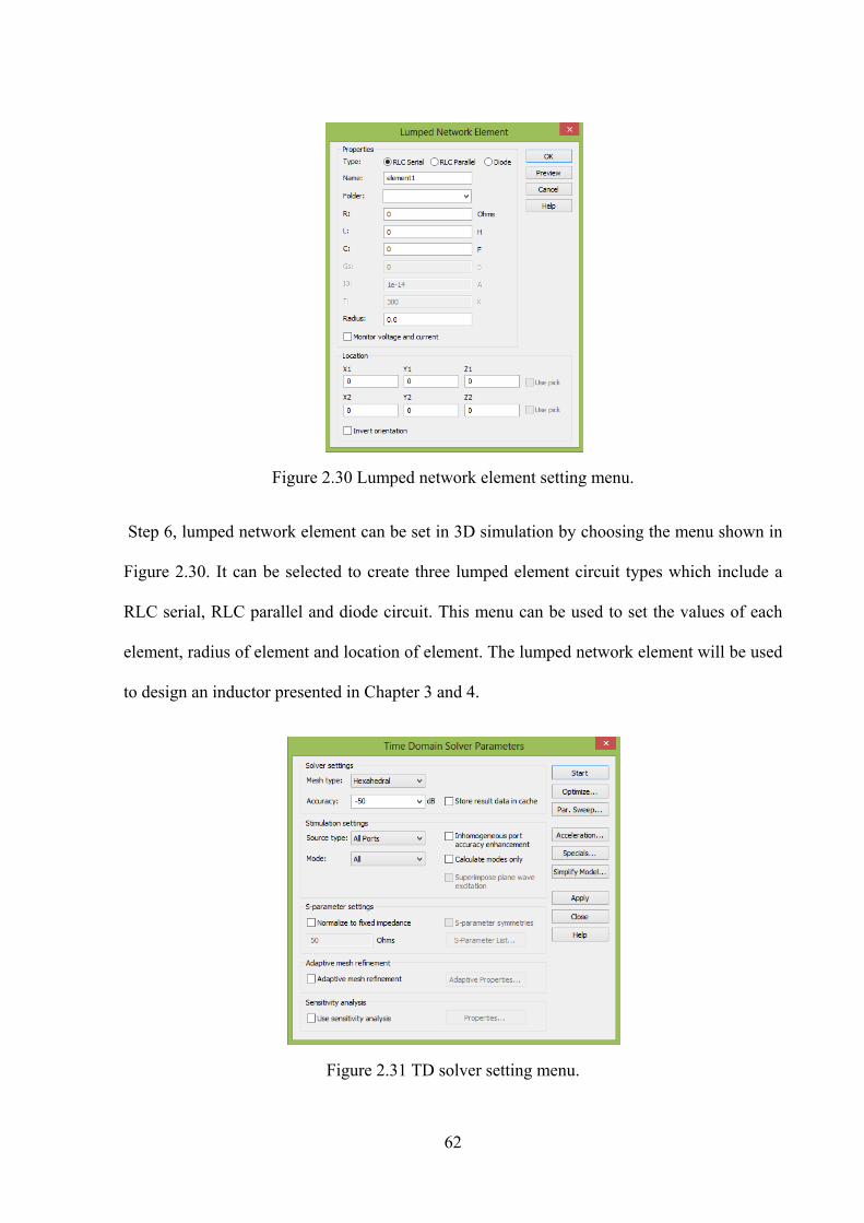
62
Figure 2.30 Lumped network element setting menu.
Step 6, lumped network element can be set in 3D simulation by choosing the menu shown in
Figure 2.30. It can be selected to create three lumped element circuit types which include a
RLC serial, RLC parallel and diode circuit. This menu can be used to set the values of each
element, radius of element and location of element. The lumped network element will be used
to design an inductor presented in Chapter 3 and 4.
Figure 2.31 TD solver setting menu.
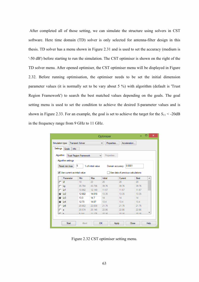
63
After completed all of those setting, we can simulate the structure using solvers in CST
software. Here time domain (TD) solver is only selected for antenna-filter design in this
thesis. TD solver has a menu shown in Figure 2.31 and is used to set the accuracy (medium is
'-50 dB') before starting to run the simulation. The CST optimiser is shown on the right of the
TD solver menu. After opened optimiser, the CST optimiser menu will be displayed in Figure
2.32. Before running optimisation, the optimiser needs to be set the initial dimension
parameter values (it is normally set to be vary about 5 %) with algorithm (default is 'Trust
Region Framework') to search the best matched values depending on the goals. The goal
setting menu is used to set the condition to achieve the desired S-parameter values and is
shown in Figure 2.33. For an example, the goal is set to achieve the target for the S11 < -20dB
in the frequency range from 9 GHz to 11 GHz.
Figure 2.32 CST optimiser setting menu.
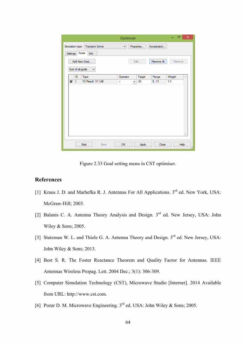
64
Figure 2.33 Goal setting menu in CST optimiser.
References
[1] Kraus J. D. and Marhefka R. J. Antennas For All Applications. 3rd ed. New York, USA:
McGraw-Hill; 2003.
[2] Balanis C. A. Antenna Theory Analysis and Design. 3rd ed. New Jersey, USA: John
Wiley & Sons; 2005.
[3] Stutzman W. L. and Thiele G. A. Antenna Theory and Design. 3rd ed. New Jersey, USA:
John Wiley & Sons; 2013.
[4] Best S. R. The Foster Reactance Theorem and Quality Factor for Antennas. IEEE
Antennas Wireless Propag. Lett. 2004 Dec.; 3(1): 306-309.
[5] Computer Simulation Technology (CST), Microwave Studio [Internet]. 2014 Available
from URL: http://www.cst.com.
[6] Pozar D. M. Microwave Engineering. 3rd ed. USA: John Wiley & Sons; 2005.

65
[7] Hong J. S. and Lancaster M. J. Microstrip Filters for RF/Microwave Applications. New
York, USA: John Wiley & Sons; 2001.
[8] Koryu Ishii T. Microwave Engineering. 2nd ed. USA: Oxford University Press; 1995.
66
Chapter 3
Two-Port Dipole Bandpass Filter
3.1 Introduction
The advantages of integrating RF/microwave components into a single module are to reduce
the microwave component count and miniaturise the total circuit area, and additionally
improve the noise and interference performance in the system. An antenna and a bandpass
filter are essential components employed at the front-end. An antenna is used for transmitting
and receiving RF signals [1], whereas a bandpass filter selects the required frequencies and
rejects unwanted frequencies. Usually the input impedance of the antenna and the output
impedance of the bandpass filter are different. A matching network is therefore required [2] to
improve power transfer. The integration of an antenna and a bandpass filter is considered here
as a new RF component called an antenna-filter.
In this chapter, a new design approach of antenna and filter integration will be started
from a bandpass filter designed using the antennas. This work is to demonstrate the antenna
elements which can serve as resonators of the filter, as well as performing their role as
radiating elements [3]. Here a dipole antenna is selected to design a resonator. The structure
of dipole is simple and can be arrayed as a side-by-side structure corresponding to the
structure of a coupled resonator filters [4]. The antenna and filter theories in [1] and [4] are
used in order to simplify the problem initially and get a good understanding in the design
approach. From a filter point of view the radiation from the antennas represent significant
source of loss for each resonator. At this stage no account is taken of the radiation pattern.
This design describes the initial concepts of an antenna-filter design based on the coupled
67
resonator filter theory. The proposed component will be called a Two-port dipole bandpass
filter. The measurements for the fabricated prototype are also presented in this chapter.
3.2 Resonator Design
This section presents a new method in the resonator design based on the structure of dipole
antennas. This work is firstly to study an equivalent circuit of a dipole antenna, which is
considered as a series resonant circuit [2]. This equivalent circuit will then be considered for
extracting the quality factor of antennas [5]. Here the quality factor of dipole is only
considered as the radiation quality factor (Qr), since the antenna is made from a lossless
material. This will be described in Section 3.2.1. The dipole antenna will be designed as a
resonator with an inductor to control the Qr and the centre frequency f0. This will be presented
in Section 3.2.2. The unloaded quality factor of resonator dipole antenna is presented in
Section 3.2.3.
3.2.1 Equivalent Circuit of Dipole Antenna in Simulation
In this section, a dipole antenna is selected and is designed at the centre frequency (f0) of 1
GHz [1]. For simplicity in the design, the dipole antenna is assumed to be made from a
lossless material (i.e. a Perfect Electric Conductor or PEC) in the CST simulation software [6]
and shown in Figure 3.1(a).
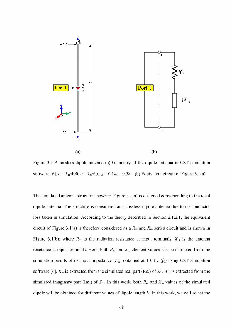
68
injX
(a) (b)
Figure 3.1 A lossless dipole antenna (a) Geometry of the dipole antenna in CST simulation
software [6]. a = 0/400, g = 0/60, ld = 0.10 – 0.50. (b) Equivalent circuit of Figure 3.1(a).
The simulated antenna structure shown in Figure 3.1(a) is designed corresponding to the ideal
dipole antenna. The structure is considered as a lossless dipole antenna due to no conductor
loss taken in simulation. According to the theory described in Section 2.1.2.1, the equivalent
circuit of Figure 3.1(a) is therefore considered as a Rin and Xin series circuit and is shown in
Figure 3.1(b); where Rin is the radiation resistance at input terminals, Xin is the antenna
reactance at input terminals. Here, both Rin and Xin element values can be extracted from the
simulation results of its input impedance (Zin) obtained at 1 GHz (f0) using CST simulation
software [6]. Rin is extracted from the simulated real part (Re.) of Zin. Xin is extracted from the
simulated imaginary part (Im.) of Zin. In this work, both Rin and Xin values of the simulated
dipole will be obtained for different values of dipole length ld. In this work, we will select the
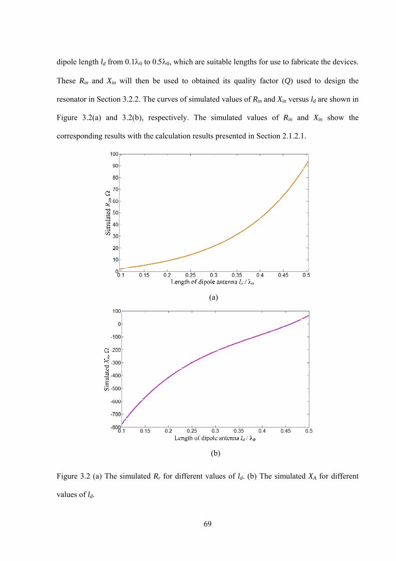
69
dipole length ld from 0.10 to 0., which are suitable lengths for use to fabricate the devices.
These Rin and Xin will then be used to obtained its quality factor (Q) used to design the
resonator in Section 3.2.2. The curves of simulated values of Rin and Xin versus ld are shown in
Figure 3.2(a) and 3.2(b), respectively. The simulated values of Rin and Xin show the
corresponding results with the calculation results presented in Section 2.1.2.1.
(a)
(b)
Figure 3.2 (a) The simulated Rr for different values of ld. (b) The simulated XA for different
values of ld.
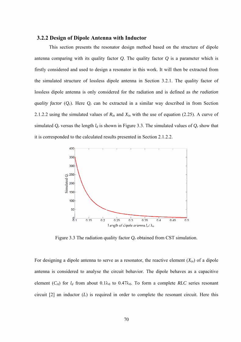
70
3.2.2 Design of Dipole Antenna with Inductor
This section presents the resonator design method based on the structure of dipole
antenna comparing with its quality factor Q. The quality factor Q is a parameter which is
firstly considered and used to design a resonator in this work. It will then be extracted from
the simulated structure of lossless dipole antenna in Section 3.2.1. The quality factor of
lossless dipole antenna is only considered for the radiation and is defined as the radiation
quality factor (Qr). Here Qr can be extracted in a similar way described in from Section
2.1.2.2 using the simulated values of Rin and Xin with the use of equation (2.25). A curve of
simulated Qr versus the length ld is shown in Figure 3.3. The simulated values of Qr show that
it is corresponded to the calculated results presented in Section 2.1.2.2.
Sim
ulat
edQ
r
Figure 3.3 The radiation quality factor Qr obtained from CST simulation.
For designing a dipole antenna to serve as a resonator, the reactive element (Xin) of a dipole
antenna is considered to analyse the circuit behavior. The dipole behaves as a capacitive
element (CA) for ld from about 0.10 to 0.470. To form a complete RLC series resonant
circuit [2] an inductor (L) is required in order to complete the resonant circuit. Here this
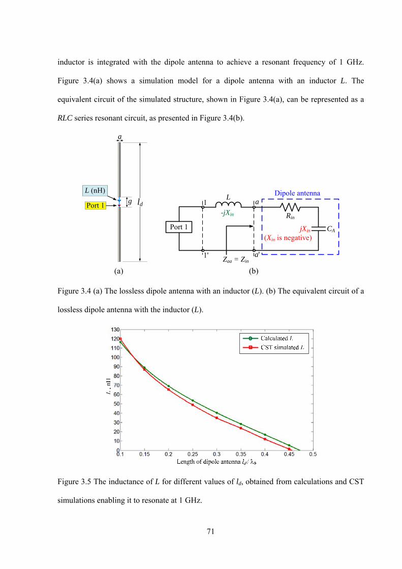
71
inductor is integrated with the dipole antenna to achieve a resonant frequency of 1 GHz.
Figure 3.4(a) shows a simulation model for a dipole antenna with an inductor L. The
equivalent circuit of the simulated structure, shown in Figure 3.4(a), can be represented as a
RLC series resonant circuit, as presented in Figure 3.4(b).
Port 1
L (nH)
ldg
a
L
Rin
CA
-jXin
jXin
(Xin is negative)
Dipole antenna
Port 1
1
1' Zaa = Zin
a
a'
(a) (b)
Figure 3.4 (a) The lossless dipole antenna with an inductor (L). (b) The equivalent circuit of a
lossless dipole antenna with the inductor (L).
Figure 3.5 The inductance of L for different values of ld, obtained from calculations and CST
simulations enabling it to resonate at 1 GHz.
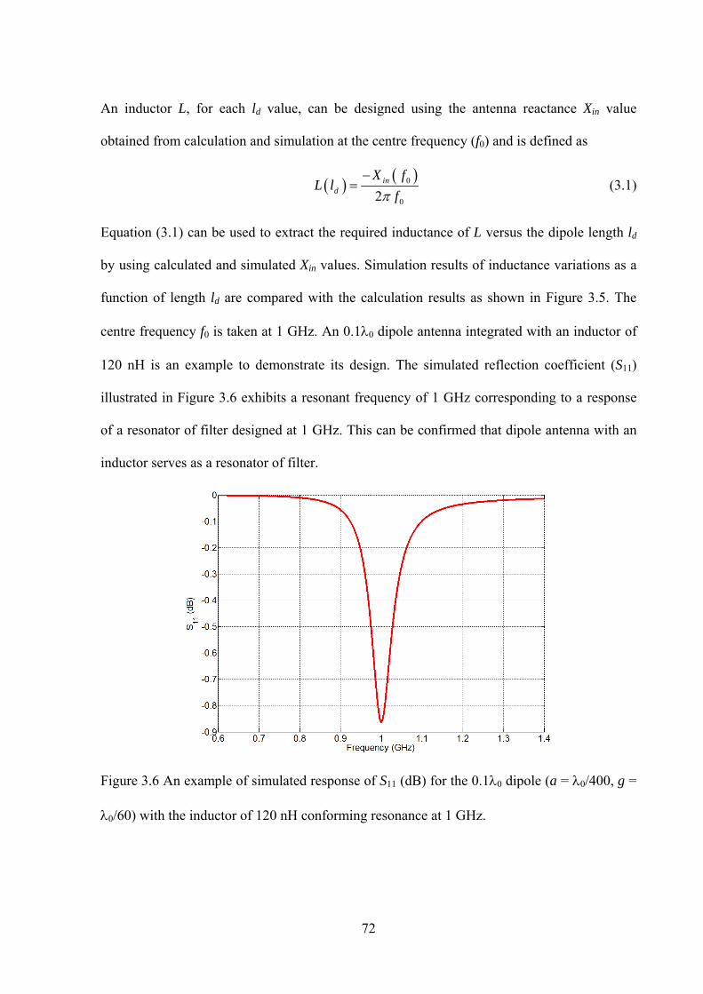
72
An inductor L, for each ld value, can be designed using the antenna reactance Xin value
obtained from calculation and simulation at the centre frequency (f0) and is defined as
0
02in
d
X fL l
f
(3.1)
Equation (3.1) can be used to extract the required inductance of L versus the dipole length ld
by using calculated and simulated Xin values. Simulation results of inductance variations as a
function of length ld are compared with the calculation results as shown in Figure 3.5. The
centre frequency f0 is taken at 1 GHz. An 0.10 dipole antenna integrated with an inductor of
120 nH is an example to demonstrate its design. The simulated reflection coefficient (S11)
illustrated in Figure 3.6 exhibits a resonant frequency of 1 GHz corresponding to a response
of a resonator of filter designed at 1 GHz. This can be confirmed that dipole antenna with an
inductor serves as a resonator of filter.
Figure 3.6 An example of simulated response of S11 (dB) for the 0.10 dipole (a = 0/400, g =
0/60) with the inductor of 120 nH conforming resonance at 1 GHz.
73
3.2.3 Unloaded Quality Factor
The total unloaded quality factor of a resonator (a dipole antenna with an inductor) may be
defined by adding these losses as follows [4],
1 1 1 1
u c r indQ Q Q Q (3.2)
where Qc, Qr, Qind are the conductor, radiation and inductor quality factors, respectively.
In this work, the dipole antenna is made from copper. This is associated with the loss
resistance (Rl) of antennas, which is considered to obtain the quality factor Qc described in
Section 2.1.2.1. The loss resistance Rl of a dipole antenna is calculated using equation (2.17).
The Rl value will then be used instead of Rin (f0) in equation (2.25) to obtained Qc of dipole
antenna. For example, the calculated Rl value for a 0.10 dipole antenna operating at 1 GHz is
found using equation (2.17), to be 0.0175 ohms. The calculated Rl is employed to calculate
the Qc value, using equation (2.25). The calculated Qc is about 4.9x10⁴. It implies that the Qc
value has negligible effect on the total unloaded Q of resonator. Thus, the total unloaded Q
factor of a resonator (a dipole antenna with an inductor) can be defined as
1 1 1
u ind rQ Q Q (3.3)
where Qr obtained from simulation is 380 for a 0.10 dipole antenna and the Qind can be
obtained from the physical dimensions of the inductor and is 320, which will be described in
Section 3.4. Thus, the total Qu results as 174.
3.3 Design of Two-Port Dipole Bandpass Filter
A new design of a third-order bandpass filter using dipole antennas is presented in this
section. The proposed component is designed using the concept of conventional coupled
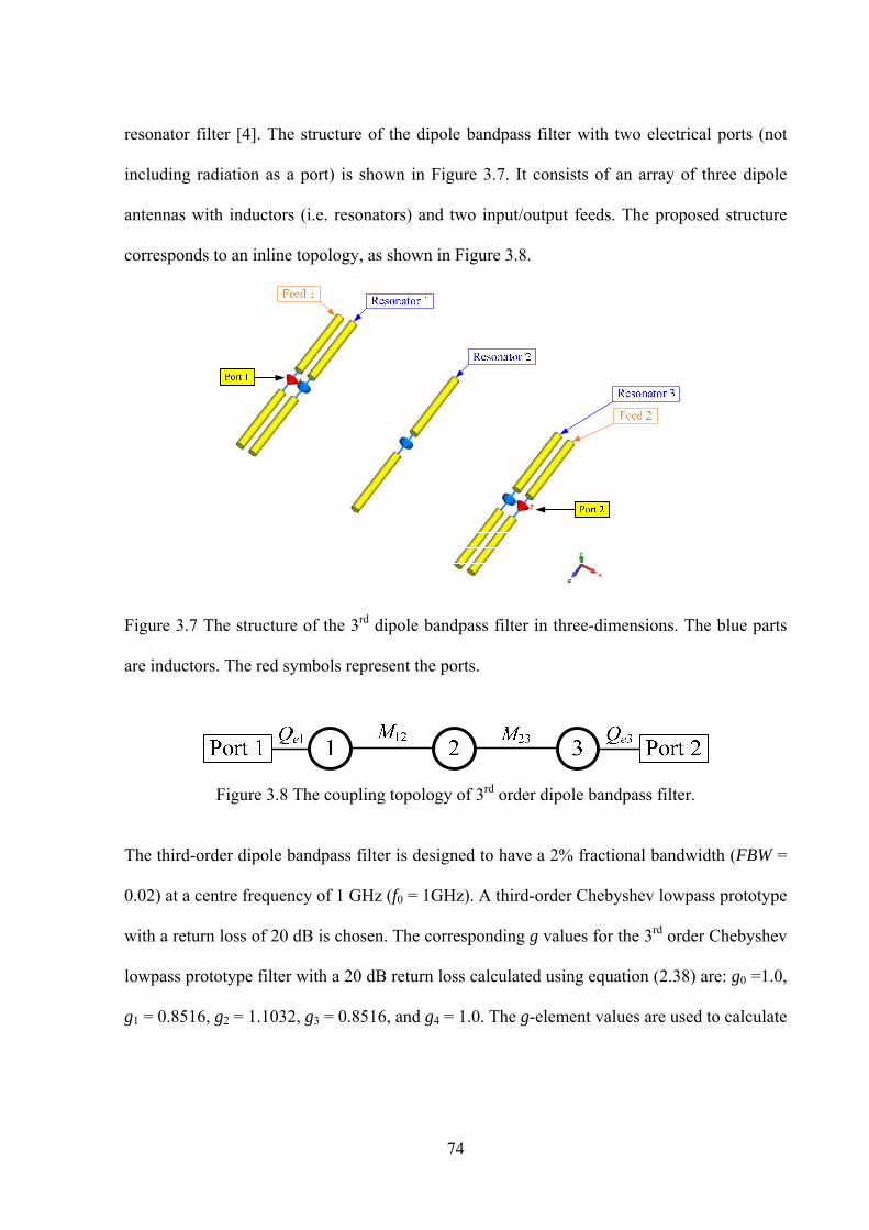
74
resonator filter [4]. The structure of the dipole bandpass filter with two electrical ports (not
including radiation as a port) is shown in Figure 3.7. It consists of an array of three dipole
antennas with inductors (i.e. resonators) and two input/output feeds. The proposed structure
corresponds to an inline topology, as shown in Figure 3.8.
Figure 3.7 The structure of the 3rd dipole bandpass filter in three-dimensions. The blue parts
are inductors. The red symbols represent the ports.
Figure 3.8 The coupling topology of 3rd order dipole bandpass filter.
The third-order dipole bandpass filter is designed to have a 2% fractional bandwidth (FBW =
0.02) at a centre frequency of 1 GHz (f0 = 1GHz). A third-order Chebyshev lowpass prototype
with a return loss of 20 dB is chosen. The corresponding g values for the 3rd order Chebyshev
lowpass prototype filter with a 20 dB return loss calculated using equation (2.38) are: g0 =1.0,
g1 = 0.8516, g2 = 1.1032, g3 = 0.8516, and g4 = 1.0. The g-element values are used to calculate
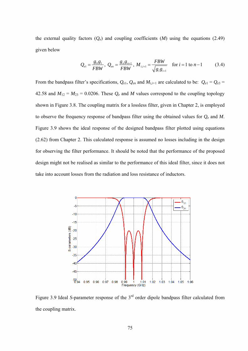
75
the external quality factors (Qe) and coupling coefficients (M) using the equations (2.49)
given below
0 1 11 , 1
1
, , for 1 to 1n ne en i i
i i
g g g g FBWQ Q M i n
FBW FBW g g
(3.4)
From the bandpass filter’s specifications, Qe1, Qen and Mi,i+1 are calculated to be: Qe1 = Qe3 =
42.58 and M12 = M23 = 0.0206. These Qe and M values correspond to the coupling topology
shown in Figure 3.8. The coupling matrix for a lossless filter, given in Chapter 2, is employed
to observe the frequency response of bandpass filter using the obtained values for Qe and M.
Figure 3.9 shows the ideal response of the designed bandpass filter plotted using equations
(2.62) from Chapter 2. This calculated response is assumed no losses including in the design
for observing the filter performance. It should be noted that the performance of the proposed
design might not be realised as similar to the performance of this ideal filter, since it does not
take into account losses from the radiation and loss resistance of inductors.
Figure 3.9 Ideal S-parameter response of the 3rd order dipole bandpass filter calculated from
the coupling matrix.
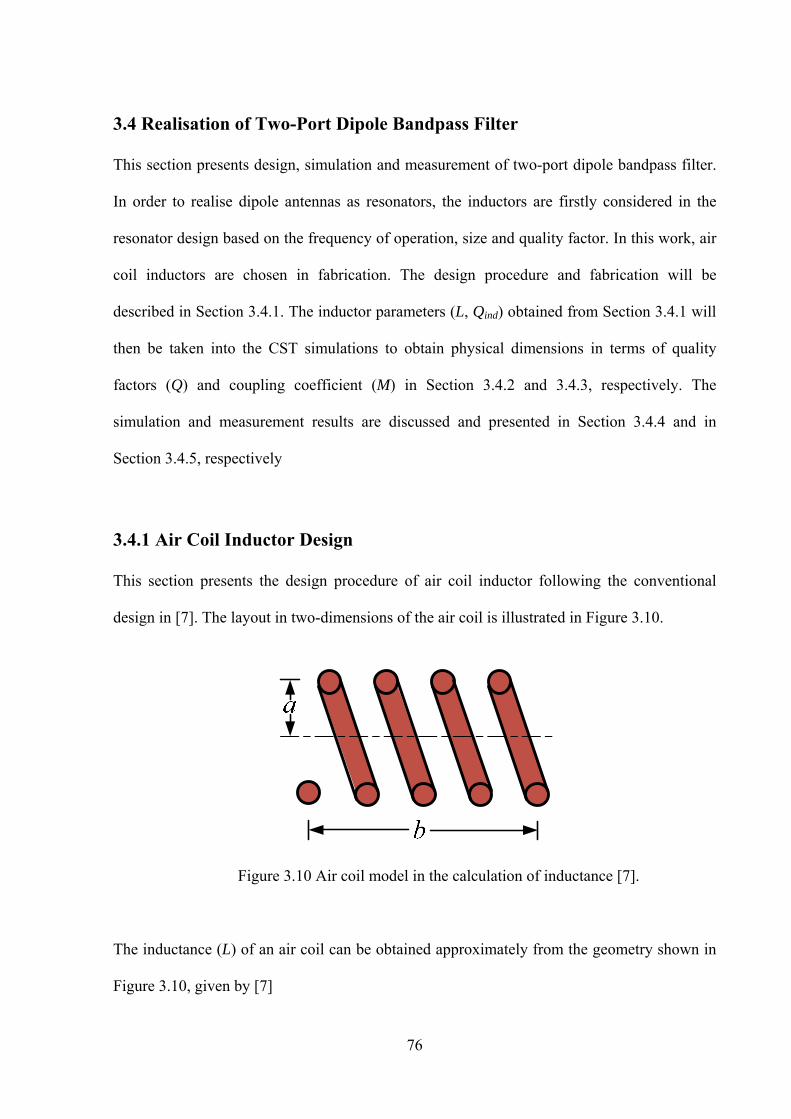
76
3.4 Realisation of Two-Port Dipole Bandpass Filter
This section presents design, simulation and measurement of two-port dipole bandpass filter.
In order to realise dipole antennas as resonators, the inductors are firstly considered in the
resonator design based on the frequency of operation, size and quality factor. In this work, air
coil inductors are chosen in fabrication. The design procedure and fabrication will be
described in Section 3.4.1. The inductor parameters (L, Qind) obtained from Section 3.4.1 will
then be taken into the CST simulations to obtain physical dimensions in terms of quality
factors (Q) and coupling coefficient (M) in Section 3.4.2 and 3.4.3, respectively. The
simulation and measurement results are discussed and presented in Section 3.4.4 and in
Section 3.4.5, respectively
3.4.1 Air Coil Inductor Design
This section presents the design procedure of air coil inductor following the conventional
design in [7]. The layout in two-dimensions of the air coil is illustrated in Figure 3.10.
Figure 3.10 Air coil model in the calculation of inductance [7].
The inductance (L) of an air coil can be obtained approximately from the geometry shown in
Figure 3.10, given by [7]
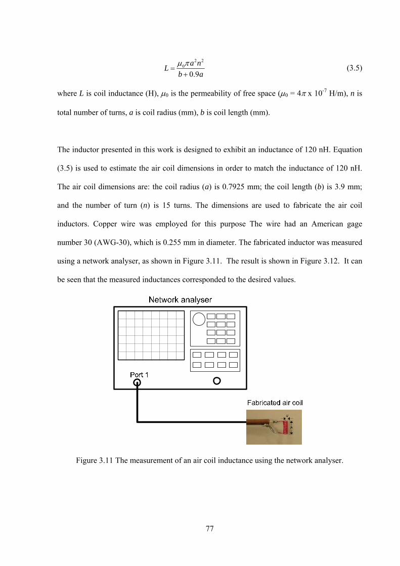
77
2 20
0.9
a nL
b a
(3.5)
where L is coil inductance (H), 0 is the permeability of free space (0 = 4 x 10⁻⁷ H/m), n is
total number of turns, a is coil radius (mm), b is coil length (mm).
The inductor presented in this work is designed to exhibit an inductance of 120 nH. Equation
(3.5) is used to estimate the air coil dimensions in order to match the inductance of 120 nH.
The air coil dimensions are: the coil radius (a) is 0.7925 mm; the coil length (b) is 3.9 mm;
and the number of turn (n) is 15 turns. The dimensions are used to fabricate the air coil
inductors. Copper wire was employed for this purpose The wire had an American gage
number 30 (AWG-30), which is 0.255 mm in diameter. The fabricated inductor was measured
using a network analyser, as shown in Figure 3.11. The result is shown in Figure 3.12. It can
be seen that the measured inductances corresponded to the desired values.
Figure 3.11 The measurement of an air coil inductance using the network analyser.
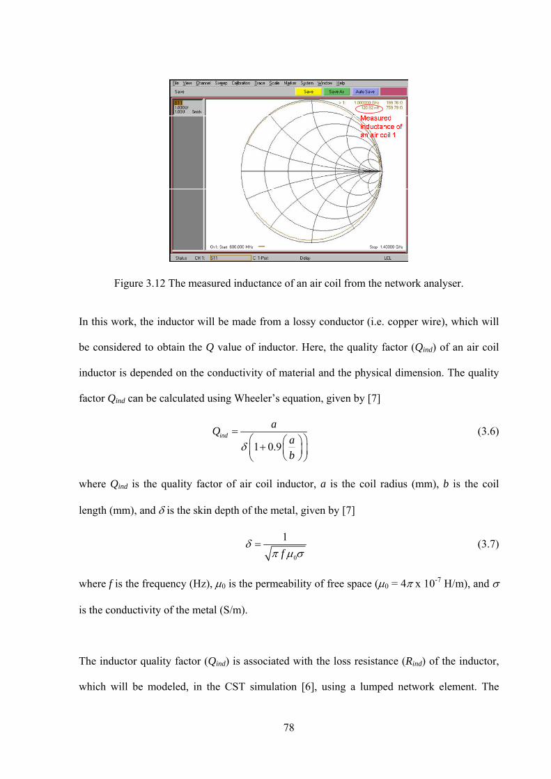
78
Figure 3.12 The measured inductance of an air coil from the network analyser.
In this work, the inductor will be made from a lossy conductor (i.e. copper wire), which will
be considered to obtain the Q value of inductor. Here, the quality factor (Qind) of an air coil
inductor is depended on the conductivity of material and the physical dimension. The quality
factor Qind can be calculated using Wheeler’s equation, given by [7]
1 0.9ind
aQ
ab
(3.6)
where Qind is the quality factor of air coil inductor, a is the coil radius (mm), b is the coil
length (mm), and is the skin depth of the metal, given by [7]
0
1
f
(3.7)
where f is the frequency (Hz), 0 is the permeability of free space (0 = 4 x 10⁻⁷ H/m), and
is the conductivity of the metal (S/m).
The inductor quality factor (Qind) is associated with the loss resistance (Rind) of the inductor,
which will be modeled, in the CST simulation [6], using a lumped network element. The
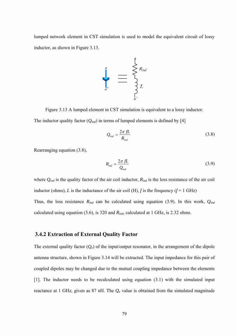
79
lumped network element in CST simulation is used to model the equivalent circuit of lossy
inductor, as shown in Figure 3.13.
Figure 3.13 A lumped element in CST simulation is equivalent to a lossy inductor.
The inductor quality factor (Qind) in terms of lumped elements is defined by [4]
2ind
ind
fLQ
R
(3.8)
Rearranging equation (3.8),
2ind
ind
fLR
Q
(3.9)
where Qind is the quality factor of the air coil inductor, Rind is the loss resistance of the air coil
inductor (ohms), L is the inductance of the air coil (H), f is the frequency (f = 1 GHz)
Thus, the loss resistance Rind can be calculated using equation (3.9). In this work, Qind
calculated using equation (3.6), is 320 and Rind, calculated at 1 GHz, is 2.32 ohms.
3.4.2 Extraction of External Quality Factor
The external quality factor (Qe) of the input/output resonator, in the arrangement of the dipole
antenna structure, shown in Figure 3.14 will be extracted. The input impedance for this pair of
coupled dipoles may be changed due to the mutual coupling impedance between the elements
[1]. The inductor needs to be recalculated using equation (3.1) with the simulated input
reactance at 1 GHz, given as 87 nH. The Qe value is obtained from the simulated magnitude
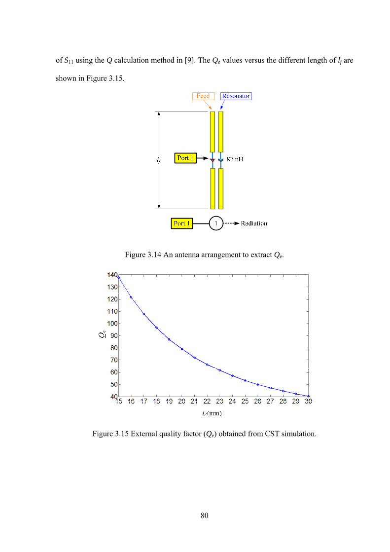
80
of S11 using the Q calculation method in [9]. The Qe values versus the different length of lf are
shown in Figure 3.15.
Figure 3.14 An antenna arrangement to extract Qe.
Figure 3.15 External quality factor (Qe) obtained from CST simulation.
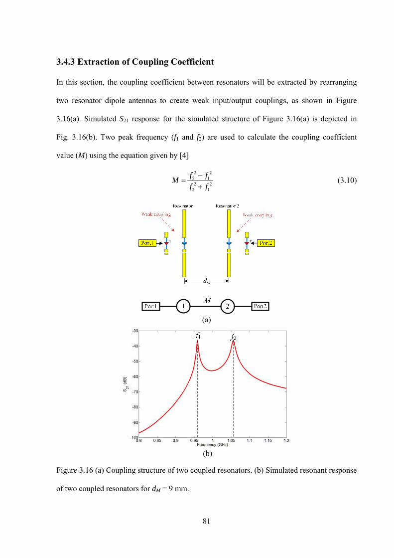
81
3.4.3 Extraction of Coupling Coefficient
In this section, the coupling coefficient between resonators will be extracted by rearranging
two resonator dipole antennas to create weak input/output couplings, as shown in Figure
3.16(a). Simulated S21 response for the simulated structure of Figure 3.16(a) is depicted in
Fig. 3.16(b). Two peak frequency (f1 and f2) are used to calculate the coupling coefficient
value (M) using the equation given by [4]
2 22 12 2
2 1
f fM
f f
(3.10)
(a)
(b)
Figure 3.16 (a) Coupling structure of two coupled resonators. (b) Simulated resonant response
of two coupled resonators for dM = 9 mm.
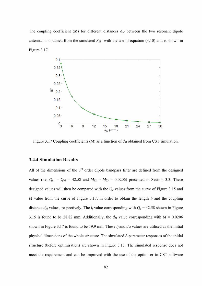
82
The coupling coefficient (M) for different distances dM between the two resonant dipole
antennas is obtained from the simulated S21 with the use of equation (3.10) and is shown in
Figure 3.17. M
Figure 3.17 Coupling coefficients (M) as a function of dM obtained from CST simulation.
3.4.4 Simulation Results
All of the dimensions of the 3rd order dipole bandpass filter are defined from the designed
values (i.e. Qe1 = Qe3 = 42.58 and M12 = M23 = 0.0206) presented in Section 3.3. These
designed values will then be compared with the Qe values from the curve of Figure 3.15 and
M value from the curve of Figure 3.17, in order to obtain the length lf and the coupling
distance dM values, respectively. The lf value corresponding with Qe = 42.58 shown in Figure
3.15 is found to be 28.82 mm. Additionally, the dM value corresponding with M = 0.0206
shown in Figure 3.17 is found to be 19.9 mm. These lf and dM values are utilised as the initial
physical dimensions of the whole structure. The simulated S-parameter responses of the initial
structure (before optimisation) are shown in Figure 3.18. The simulated response does not
meet the requirement and can be improved with the use of the optimiser in CST software
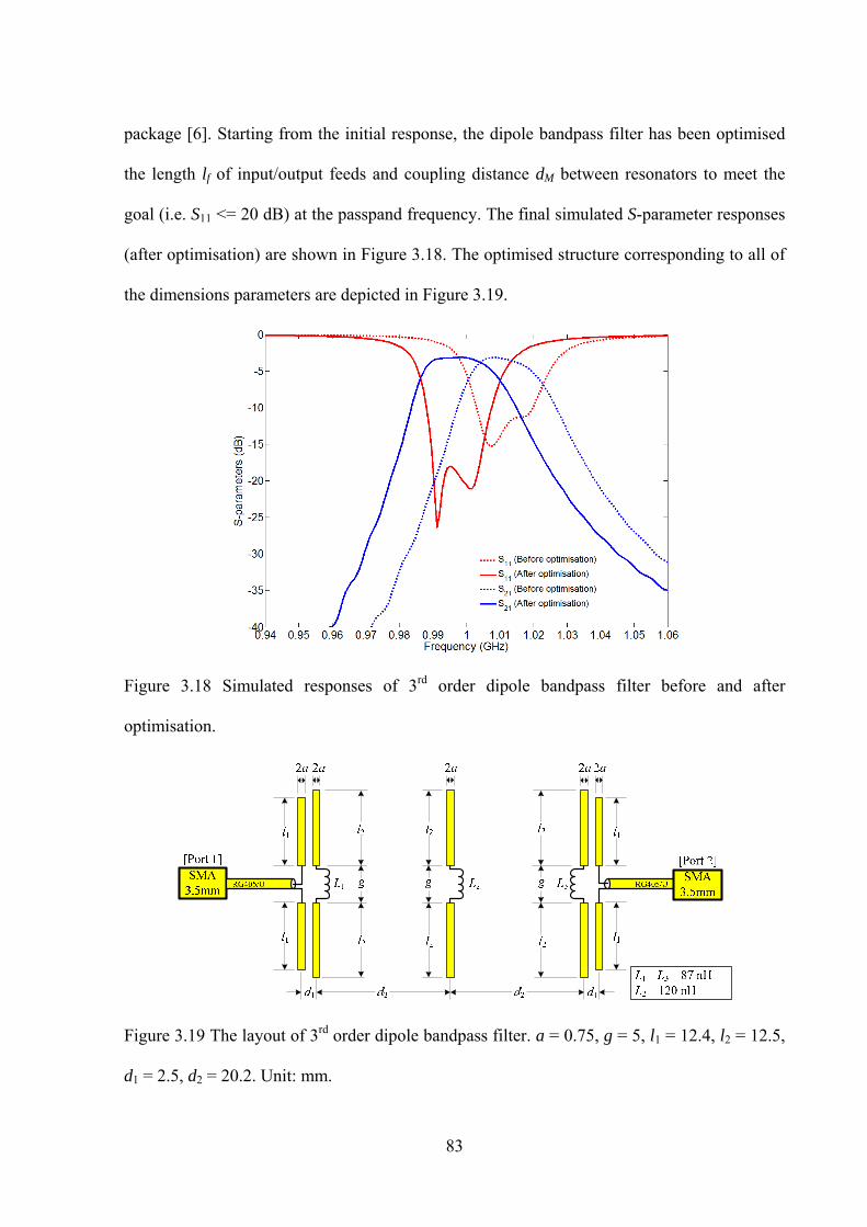
83
package [6]. Starting from the initial response, the dipole bandpass filter has been optimised
the length lf of input/output feeds and coupling distance dM between resonators to meet the
goal (i.e. S11 <= 20 dB) at the passpand frequency. The final simulated S-parameter responses
(after optimisation) are shown in Figure 3.18. The optimised structure corresponding to all of
the dimensions parameters are depicted in Figure 3.19.
Figure 3.18 Simulated responses of 3rd order dipole bandpass filter before and after
optimisation.
Figure 3.19 The layout of 3rd order dipole bandpass filter. a = 0.75, g = 5, l1 = 12.4, l2 = 12.5,
d1 = 2.5, d2 = 20.2. Unit: mm.
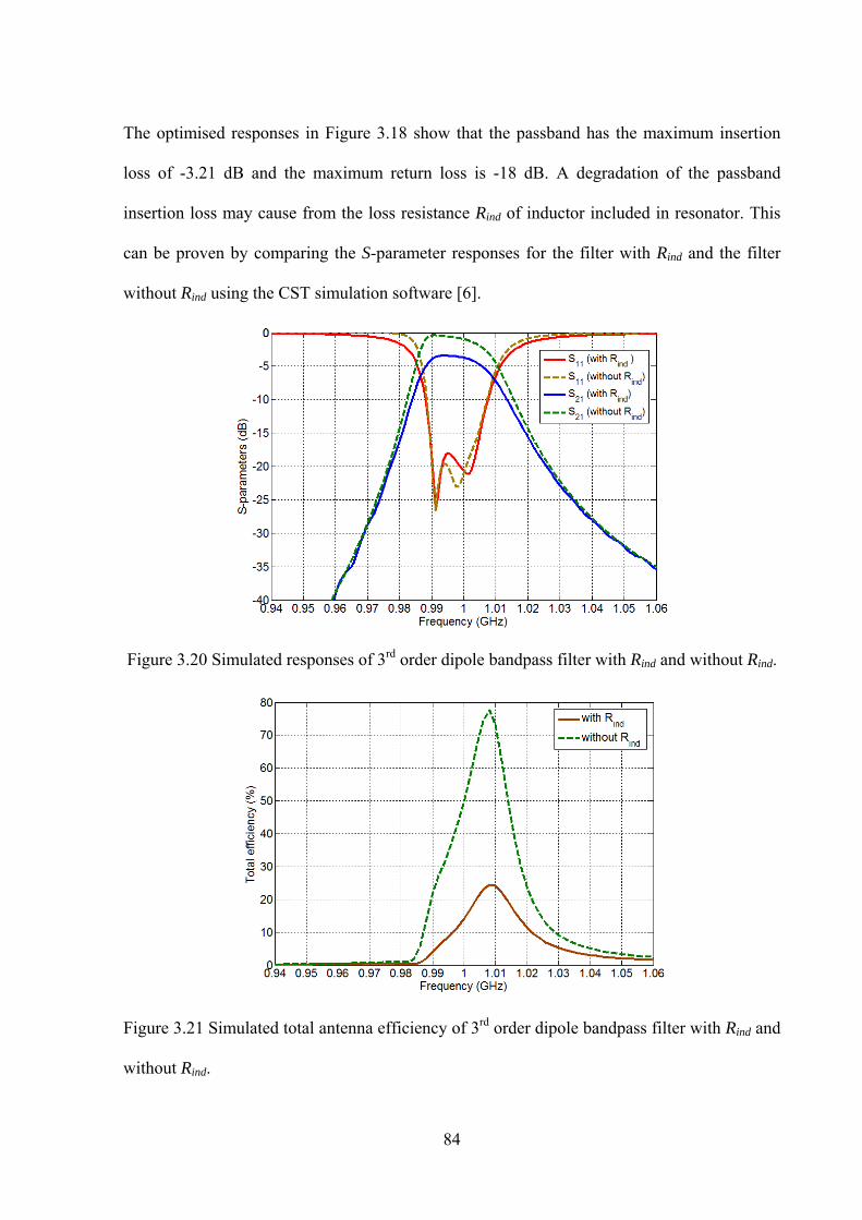
84
The optimised responses in Figure 3.18 show that the passband has the maximum insertion
loss of -3.21 dB and the maximum return loss is -18 dB. A degradation of the passband
insertion loss may cause from the loss resistance Rind of inductor included in resonator. This
can be proven by comparing the S-parameter responses for the filter with Rind and the filter
without Rind using the CST simulation software [6].
Figure 3.20 Simulated responses of 3rd order dipole bandpass filter with Rind and without Rind.
Figure 3.21 Simulated total antenna efficiency of 3rd order dipole bandpass filter with Rind and
without Rind.
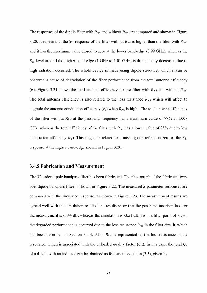
85
The responses of the dipole filter with Rind and without Rind are compared and shown in Figure
3.20. It is seen that the S21 response of the filter without Rind is higher than the filter with Rind,
and it has the maximum value closed to zero at the lower band-edge (0.99 GHz), whereas the
S21 level around the higher band-edge (1 GHz to 1.01 GHz) is dramatically decreased due to
high radiation occurred. The whole device is made using dipole structure, which it can be
observed a cause of degradation of the filter performance from the total antenna efficiency
(et). Figure 3.21 shows the total antenna efficiency for the filter with Rind and without Rind.
The total antenna efficiency is also related to the loss resistance Rind which will affect to
degrade the antenna conduction efficiency (ec) when Rind is high. The total antenna efficiency
of the filter without Rind at the passband frequency has a maximum value of 77% at 1.008
GHz, whereas the total efficiency of the filter with Rind has a lower value of 25% due to low
conduction efficiency (ec). This might be related to a missing one reflection zero of the S11
response at the higher band-edge shown in Figure 3.20.
3.4.5 Fabrication and Measurement
The 3rd order dipole bandpass filter has been fabricated. The photograph of the fabricated two-
port dipole bandpass filter is shown in Figure 3.22. The measured S-parameter responses are
compared with the simulated response, as shown in Figure 3.23. The measurement results are
agreed well with the simulation results. The results show that the passband insertion loss for
the measurement is -3.44 dB, whereas the simulation is -3.21 dB. From a filter point of view ,
the degraded performance is occurred due to the loss resistance Rind in the filter circuit, which
has been described in Section 3.4.4. Also, Rind is represented as the loss resistance in the
resonator, which is associated with the unloaded quality factor (Qu). In this case, the total Qu
of a dipole with an inductor can be obtained as follows an equation (3.3), given by
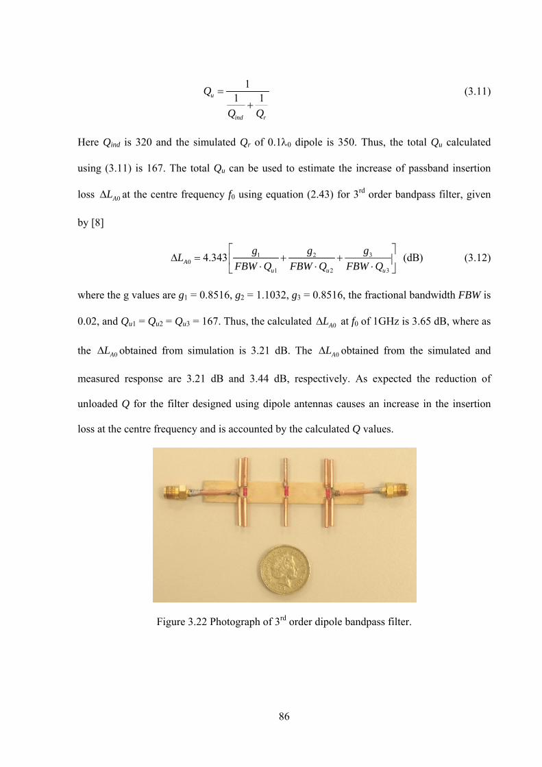
Here
using
loss
by [8
wher
0.02,
the
meas
unloa
loss a
e Qind is 320
g (3.11) is
0AL at the
8]
re the g valu
, and Qu1 =
0AL obtain
sured respo
aded Q for
at the centre
0 and the s
167. The to
centre freq
0AL
ues are g1 =
Qu2 = Qu3 =
ed from sim
onse are 3.2
the filter d
e frequency
Figure 3.
1u
ind
Q
Q
simulated Q
otal Qu can
quency f0 us
4.343FB
= 0.8516, g2
= 167. Thus
mulation is
21 dB and
designed us
y and is acco
22 Photogra
86
11
rQ
Qr of 0.10
be used to
sing equatio
1
1u
g
BW Q F
= 1.1032, g
s, the calcula
s 3.21 dB.
3.44 dB,
ing dipole
ounted by th
aph of 3rd o
dipole is 3
o estimate th
on (2.43) fo
2
2u
g
FBW Q
g3 = 0.8516
ated 0AL a
The 0AL o
respectively
antennas ca
he calculate
order dipole
50. Thus, t
he increase
or 3rd order
3
3u
g
FBW Q
, the fractio
at f0 of 1GH
obtained fro
y. As expe
auses an in
ed Q values.
bandpass fi
the total Qu
of passban
bandpass f
(dB)
onal bandwi
Hz is 3.65 dB
om the sim
ected the re
crease in th
.
filter.
(3.11)
u calculated
nd insertion
filter, given
(3.12)
idth FBW is
B, where as
mulated and
eduction of
he insertion
)
d
n
n
)
s
s
d
f
n
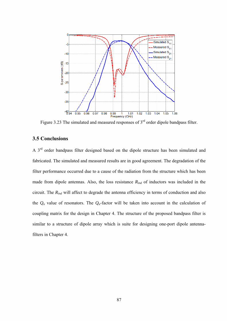
87
Figure 3.23 The simulated and measured responses of 3rd order dipole bandpass filter.
3.5 Conclusions
A 3rd order bandpass filter designed based on the dipole structure has been simulated and
fabricated. The simulated and measured results are in good agreement. The degradation of the
filter performance occurred due to a cause of the radiation from the structure which has been
made from dipole antennas. Also, the loss resistance Rind of inductors was included in the
circuit. The Rind will affect to degrade the antenna efficiency in terms of conduction and also
the Qu value of resonators. The Qu-factor will be taken into account in the calculation of
coupling matrix for the design in Chapter 4. The structure of the proposed bandpass filter is
similar to a structure of dipole array which is suite for designing one-port dipole antenna-
filters in Chapter 4.
88
References
[1] Balanis C. A. Antenna Theory Analysis and Design. 3rd ed. New Jersey, USA: John
Wiley & Sons; 2005.
[2] Pozar D. M. Microwave Engineering. 3rd ed. USA: John Wiley & Sons; 2005.
[3] Chang K., York R. A., Hall P. S., Itoh T. Active integrated antennas. IEEE Trans.
Microw. Theory Techn. 2002 Mar.; 50(3): 937-943.
[4] Hong J. S. and Lancaster M. J. Microstrip Filters for RF/Microwave Applications. New
York, USA: John Wiley & Sons; 2001.
[5] Best S. R. The Foster Reactance Theorem and Quality Factor for Antennas. IEEE
Antennas Wireless Propag. Lett. 2004 Dec.; 3(1): 306-309.
[6] Computer Simulation Technology (CST), Microwave Studio [Internet]. 2014 Available
from URL: http://www.cst.com.
[7] Wheeler H. A. Formulas for the Skin Effect. Proceedings of the IRE. 1942 Sep.; 30(9):
412-424.
[8] Lancaster M. J. Passive Microwave Device Applications of High-Temperature
Superconductors. Cambridge, UK: Cambridge University Press; 1997.
89
Chapter 4
One-Port Dipole Antenna-Filter
4.1 Introduction
In Chapter 3, a two-port dipole bandpass filter was designed based on the concept of coupled
resonator filter theory [1]. In this chapter, the design method of the two-port dipole bandpass
filter can be applied to the one-port dipole antenna-filter design (with radiation not considered
as a port). This chapter presents the three new designs of dipole antennas and bandpass filters
integrated into a single module using the coupling matrix synthesis. The coupling matrix can
be utilised to optimise design parameters (coupling coefficients and external quality factor) in
order to improve the frequency response corresponding to the specifications. The optimised
parameters will then be utilised to find the physical dimensions of dipole antenna-filters using
standard techniques [1]. The work presented in this chapter has been divided in three sections
as follows. Section 4.2 presents a one-resonator dipole antenna-filter in order to understand
the basic idea with the simplest antenna-filter. Section 4.3 presents a two-resonator dipole
antenna-filter. The two-resonator design provides improved passband return loss S11 and the
realised gain of the antenna-filter. Section 4.4 presents a three-resonator dipole antenna-filter.
Each of these three sections includes the design method using the coupling matrix, the
calculation and simulation results, and fabrication and measurement. The conclusion is
provided in Section 4.5.
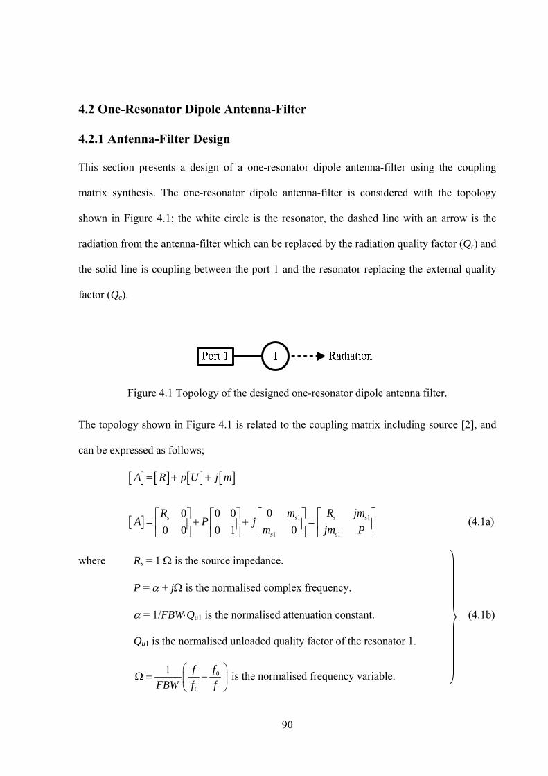
90
4.2 One-Resonator Dipole Antenna-Filter
4.2.1 Antenna-Filter Design
This section presents a design of a one-resonator dipole antenna-filter using the coupling
matrix synthesis. The one-resonator dipole antenna-filter is considered with the topology
shown in Figure 4.1; the white circle is the resonator, the dashed line with an arrow is the
radiation from the antenna-filter which can be replaced by the radiation quality factor (Qr) and
the solid line is coupling between the port 1 and the resonator replacing the external quality
factor (Qe).
Figure 4.1 Topology of the designed one-resonator dipole antenna filter.
The topology shown in Figure 4.1 is related to the coupling matrix including source [2], and
can be expressed as follows;
1 1
1 1
00 0 0 (4.1a)
00 0 0 1s s ss
s s
A R p U j m
m R jmRA P j
m jm P
where Rs = 1 is the source impedance.
P = + j is the normalised complex frequency.
= 1/FBWQu1 is the normalised attenuation constant. (4.1b)
Qu1 is the normalised unloaded quality factor of the resonator 1.
0
0
1 ff
FBW f f
is the normalised frequency variable.
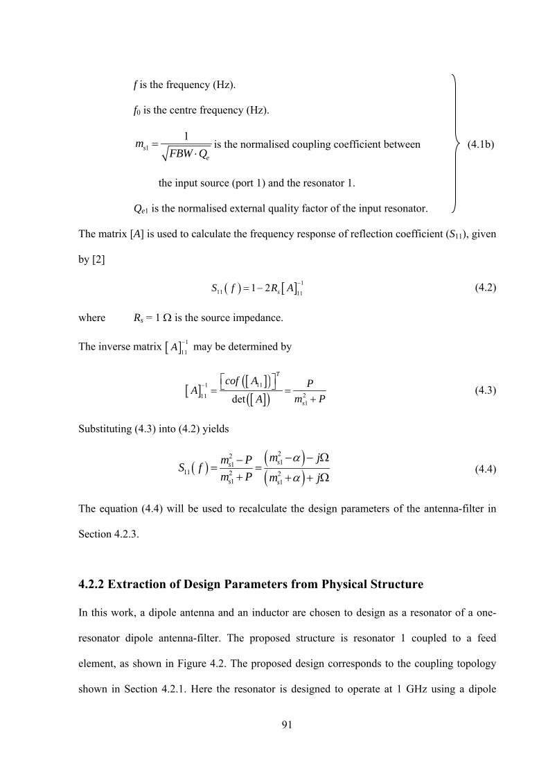
91
f is the frequency (Hz).
f0 is the centre frequency (Hz).
1
1s
e
mFBW Q
is the normalised coupling coefficient between (4.1b)
the input source (port 1) and the resonator 1.
Qe1 is the normalised external quality factor of the input resonator.
The matrix [A] is used to calculate the frequency response of reflection coefficient (S11), given
by [2]
1
11 111 2 sS f R A
(4.2)
where Rs = 1 is the source impedance.
The inverse matrix 1
11A
may be determined by
111
2111det
T
s
cof A PA
m PA
(4.3)
Substituting (4.3) into (4.2) yields
2211
11 2 21 1
ss
s s
m jm PS f
m P m j
(4.4)
The equation (4.4) will be used to recalculate the design parameters of the antenna-filter in
Section 4.2.3.
4.2.2 Extraction of Design Parameters from Physical Structure
In this work, a dipole antenna and an inductor are chosen to design as a resonator of a one-
resonator dipole antenna-filter. The proposed structure is resonator 1 coupled to a feed
element, as shown in Figure 4.2. The proposed design corresponds to the coupling topology
shown in Section 4.2.1. Here the resonator is designed to operate at 1 GHz using a dipole
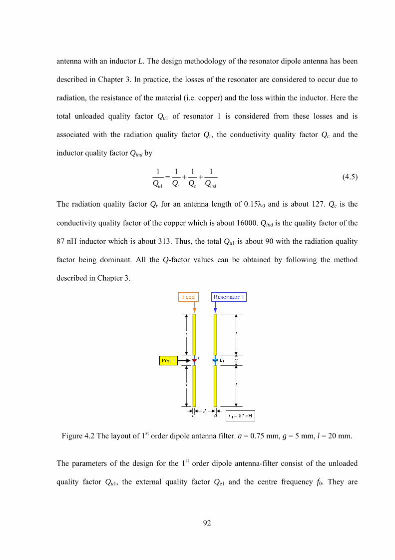
92
antenna with an inductor L. The design methodology of the resonator dipole antenna has been
described in Chapter 3. In practice, the losses of the resonator are considered to occur due to
radiation, the resistance of the material (i.e. copper) and the loss within the inductor. Here the
total unloaded quality factor Qu1 of resonator 1 is considered from these losses and is
associated with the radiation quality factor Qr, the conductivity quality factor Qc and the
inductor quality factor Qind by
1
1 1 1 1
u r c indQ Q Q Q (4.5)
The radiation quality factor Qr for an antenna length of 0.150 and is about 127. Qc is the
conductivity quality factor of the copper which is about 16000. Qind is the quality factor of the
87 nH inductor which is about 313. Thus, the total Qu1 is about 90 with the radiation quality
factor being dominant. All the Q-factor values can be obtained by following the method
described in Chapter 3.
Figure 4.2 The layout of 1st order dipole antenna filter. a = 0.75 mm, g = 5 mm, l = 20 mm.
The parameters of the design for the 1st order dipole antenna-filter consist of the unloaded
quality factor Qu1, the external quality factor Qe1 and the centre frequency f0. They are
93
extracted from the simulated response of S11 using CST simulation software [3] with the use
of Q-calculation method for the one-port component in [4].
df = 3 mmdf = 5 mmdf = 7 mmdf = 9 mmdf = 11 mmdf = 13 mmdf = 15 mm
(a)
(b)
Figure 4.3 (a) Simulated S11 responses of the structure in Figure 4.2 for different values of df.
(b) Simulated Qe1, Qu1 and f0 values for different values of df.
This structure can tune the S11 response by moving the feed or adjusting the separation df. The
simulated S11 response of the 1st order dipole antenna-filter for different value of df is shown
in Figure 4.3(a). At df = 3 mm, the S11 response of antenna-filter exhibits a large bandwidth
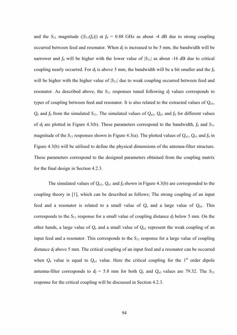
94
and the S11 magnitude (|S11(f0)|) at f0 = 0.88 GHz as about -4 dB due to strong coupling
occurred between feed and resonator. When df is increased to be 5 mm, the bandwidth will be
narrower and f0 will be higher with the lower value of |S11| as about -16 dB due to critical
coupling nearly occurred. For df is above 5 mm, the bandwidth will be a bit smaller and the f0
will be higher with the higher value of |S11| due to weak coupling occurred between feed and
resonator. As described above, the S11 responses tuned following df values corresponds to
types of coupling between feed and resonator. It is also related to the extracted values of Qu1,
Qe and f0 from the simulated S11. The simulated values of Qu1, Qe1 and f0 for different values
of df are plotted in Figure 4.3(b). These parameters correspond to the bandwidth, f0 and S11
magnitude of the S11 responses shown in Figure 4.3(a). The plotted values of Qu1, Qe1 and f0 in
Figure 4.3(b) will be utilised to define the physical dimensions of the antenna-filter structure.
These parameters correspond to the designed parameters obtained from the coupling matrix
for the final design in Section 4.2.3.
The simulated values of Qu1, Qe1 and f0 shown in Figure 4.3(b) are corresponded to the
coupling theory in [1], which can be described as follows; The strong coupling of an input
feed and a resonator is related to a small value of Qe and a large value of Qu1. This
corresponds to the S11 response for a small value of coupling distance df below 5 mm. On the
other hands, a large value of Qe and a small value of Qu1 represent the weak coupling of an
input feed and a resonator. This corresponds to the S11 response for a large value of coupling
distance df above 5 mm. The critical coupling of an input feed and a resonator can be occurred
when Qe value is equal to Qu1 value. Here the critical coupling for the 1st order dipole
antenna-filter corresponds to df = 5.8 mm for both Qe and Qu1 values are 79.32. The S11
response for the critical coupling will be discussed in Section 4.2.3.
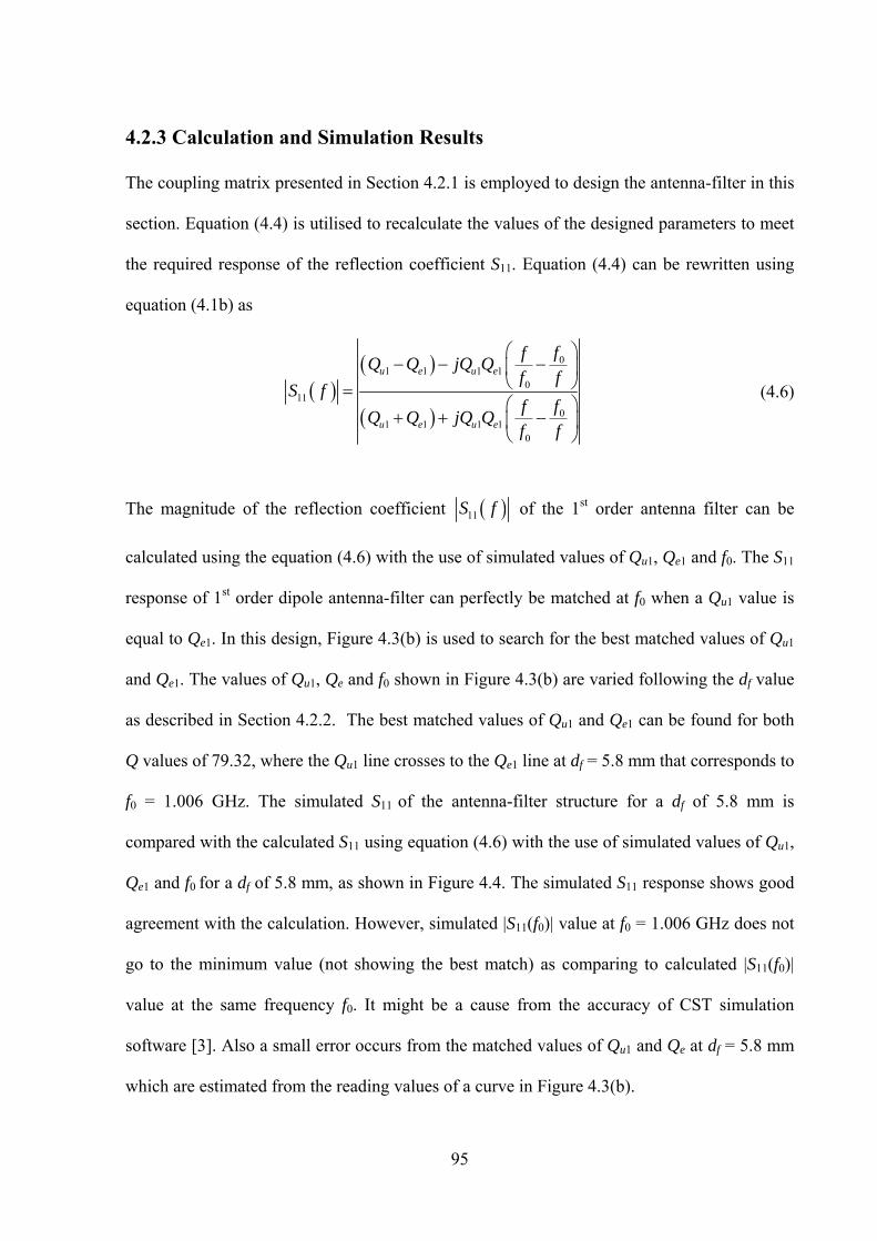
95
4.2.3 Calculation and Simulation Results
The coupling matrix presented in Section 4.2.1 is employed to design the antenna-filter in this
section. Equation (4.4) is utilised to recalculate the values of the designed parameters to meet
the required response of the reflection coefficient S11. Equation (4.4) can be rewritten using
equation (4.1b) as
01 1 1 1
011
01 1 1 1
0
u e u e
u e u e
ffQ Q jQ Q
f fS f
ffQ Q jQ Q
f f
(4.6)
The magnitude of the reflection coefficient 11S f of the 1st order antenna filter can be
calculated using the equation (4.6) with the use of simulated values of Qu1, Qe1 and f0. The S11
response of 1st order dipole antenna-filter can perfectly be matched at f0 when a Qu1 value is
equal to Qe1. In this design, Figure 4.3(b) is used to search for the best matched values of Qu1
and Qe1. The values of Qu1, Qe and f0 shown in Figure 4.3(b) are varied following the df value
as described in Section 4.2.2. The best matched values of Qu1 and Qe1 can be found for both
Q values of 79.32, where the Qu1 line crosses to the Qe1 line at df = 5.8 mm that corresponds to
f0 = 1.006 GHz. The simulated S11 of the antenna-filter structure for a df of 5.8 mm is
compared with the calculated S11 using equation (4.6) with the use of simulated values of Qu1,
Qe1 and f0 for a df of 5.8 mm, as shown in Figure 4.4. The simulated S11 response shows good
agreement with the calculation. However, simulated |S11(f0)| value at f0 = 1.006 GHz does not
go to the minimum value (not showing the best match) as comparing to calculated |S11(f0)|
value at the same frequency f0. It might be a cause from the accuracy of CST simulation
software [3]. Also a small error occurs from the matched values of Qu1 and Qe at df = 5.8 mm
which are estimated from the reading values of a curve in Figure 4.3(b).
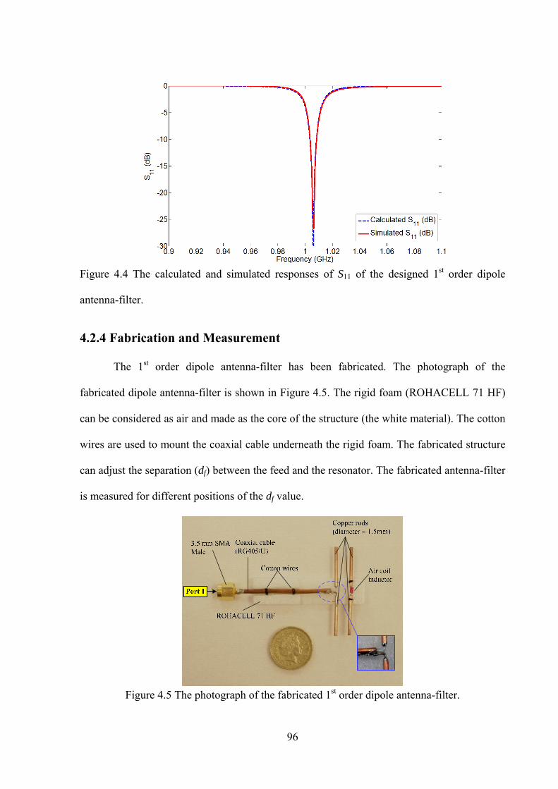
96
Figure 4.4 The calculated and simulated responses of S11 of the designed 1st order dipole
antenna-filter.
4.2.4 Fabrication and Measurement
The 1st order dipole antenna-filter has been fabricated. The photograph of the
fabricated dipole antenna-filter is shown in Figure 4.5. The rigid foam (ROHACELL 71 HF)
can be considered as air and made as the core of the structure (the white material). The cotton
wires are used to mount the coaxial cable underneath the rigid foam. The fabricated structure
can adjust the separation (df) between the feed and the resonator. The fabricated antenna-filter
is measured for different positions of the df value.
Figure 4.5 The photograph of the fabricated 1st order dipole antenna-filter.
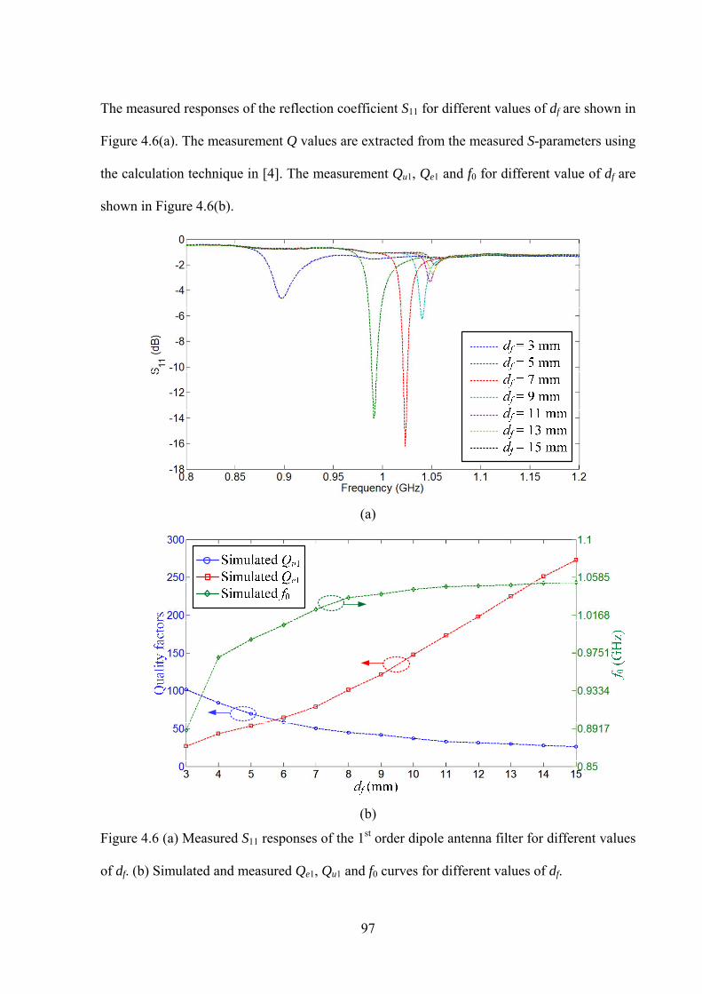
97
The measured responses of the reflection coefficient S11 for different values of df are shown in
Figure 4.6(a). The measurement Q values are extracted from the measured S-parameters using
the calculation technique in [4]. The measurement Qu1, Qe1 and f0 for different value of df are
shown in Figure 4.6(b).
(a)
(b)
Figure 4.6 (a) Measured S11 responses of the 1st order dipole antenna filter for different values
of df. (b) Simulated and measured Qe1, Qu1 and f0 curves for different values of df.
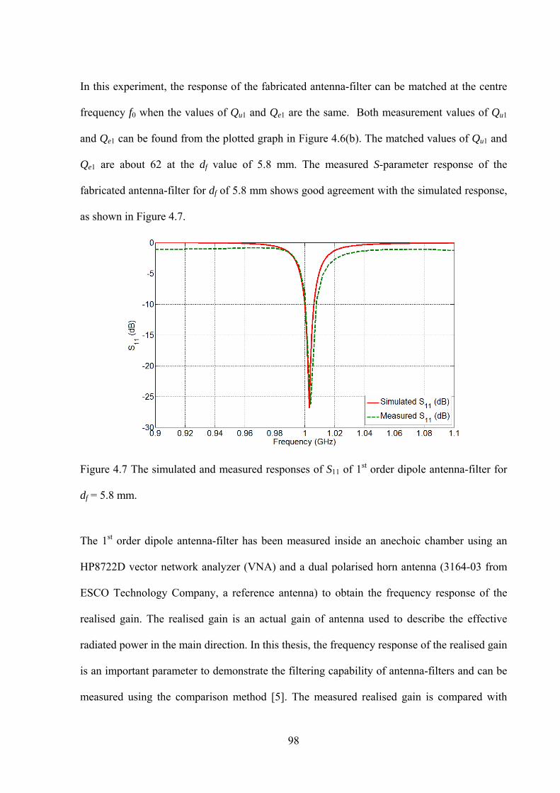
98
In this experiment, the response of the fabricated antenna-filter can be matched at the centre
frequency f0 when the values of Qu1 and Qe1 are the same. Both measurement values of Qu1
and Qe1 can be found from the plotted graph in Figure 4.6(b). The matched values of Qu1 and
Qe1 are about 62 at the df value of 5.8 mm. The measured S-parameter response of the
fabricated antenna-filter for df of 5.8 mm shows good agreement with the simulated response,
as shown in Figure 4.7.
Figure 4.7 The simulated and measured responses of S11 of 1st order dipole antenna-filter for
df = 5.8 mm.
The 1st order dipole antenna-filter has been measured inside an anechoic chamber using an
HP8722D vector network analyzer (VNA) and a dual polarised horn antenna (3164-03 from
ESCO Technology Company, a reference antenna) to obtain the frequency response of the
realised gain. The realised gain is an actual gain of antenna used to describe the effective
radiated power in the main direction. In this thesis, the frequency response of the realised gain
is an important parameter to demonstrate the filtering capability of antenna-filters and can be
measured using the comparison method [5]. The measured realised gain is compared with
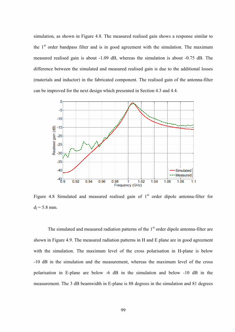
99
simulation, as shown in Figure 4.8. The measured realised gain shows a response similar to
the 1st order bandpass filter and is in good agreement with the simulation. The maximum
measured realised gain is about -1.09 dB, whereas the simulation is about -0.75 dB. The
difference between the simulated and measured realised gain is due to the additional losses
(materials and inductor) in the fabricated component. The realised gain of the antenna-filter
can be improved for the next design which presented in Section 4.3 and 4.4.
Figure 4.8 Simulated and measured realised gain of 1st order dipole antenna-filter for
df = 5.8 mm.
The simulated and measured radiation patterns of the 1st order dipole antenna-filter are
shown in Figure 4.9. The measured radiation patterns in H and E plane are in good agreement
with the simulation. The maximum level of the cross polarisation in H-plane is below
-10 dB in the simulation and the measurement, whereas the maximum level of the cross
polarisation in E-plane are below -6 dB in the simulation and below -10 dB in the
measurement. The 3 dB beamwidth in E-plane is 88 degrees in the simulation and 81 degrees
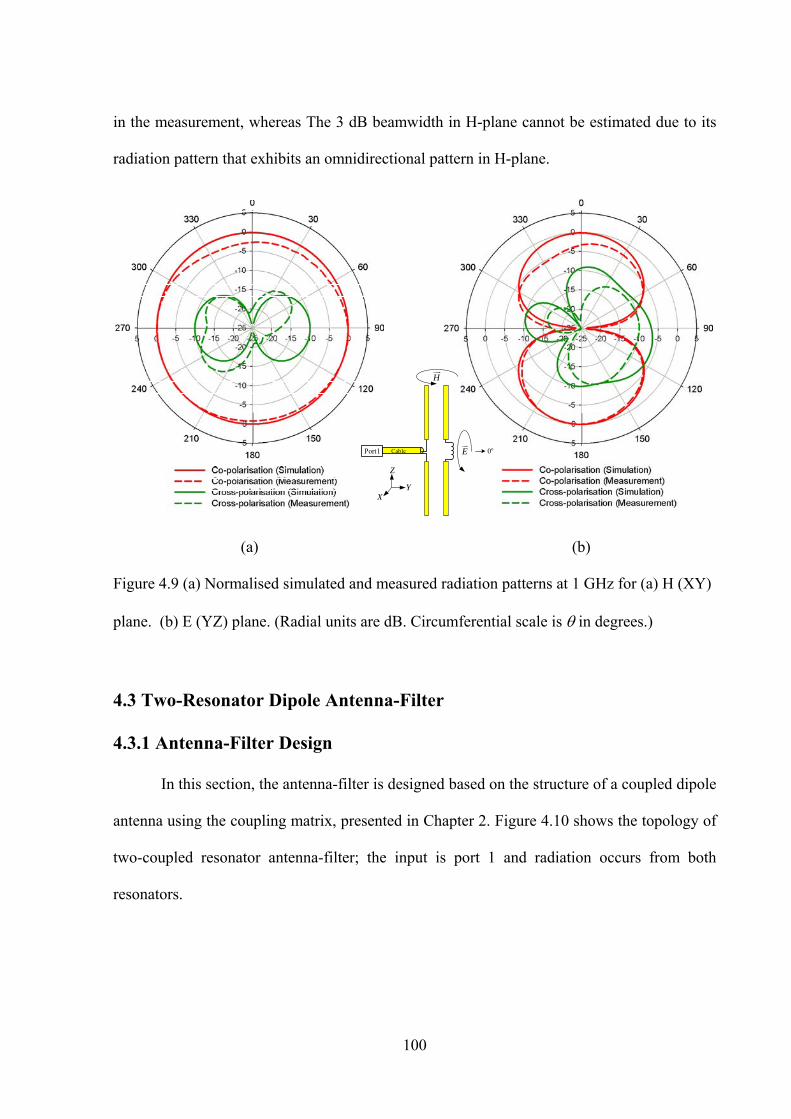
100
in the measurement, whereas The 3 dB beamwidth in H-plane cannot be estimated due to its
radiation pattern that exhibits an omnidirectional pattern in H-plane.
Port1 Cable 0o
H
E
Z
XY
(a) (b)
Figure 4.9 (a) Normalised simulated and measured radiation patterns at 1 GHz for (a) H (XY)
plane. (b) E (YZ) plane. (Radial units are dB. Circumferential scale is in degrees.)
4.3 Two-Resonator Dipole Antenna-Filter
4.3.1 Antenna-Filter Design
In this section, the antenna-filter is designed based on the structure of a coupled dipole
antenna using the coupling matrix, presented in Chapter 2. Figure 4.10 shows the topology of
two-coupled resonator antenna-filter; the input is port 1 and radiation occurs from both
resonators.
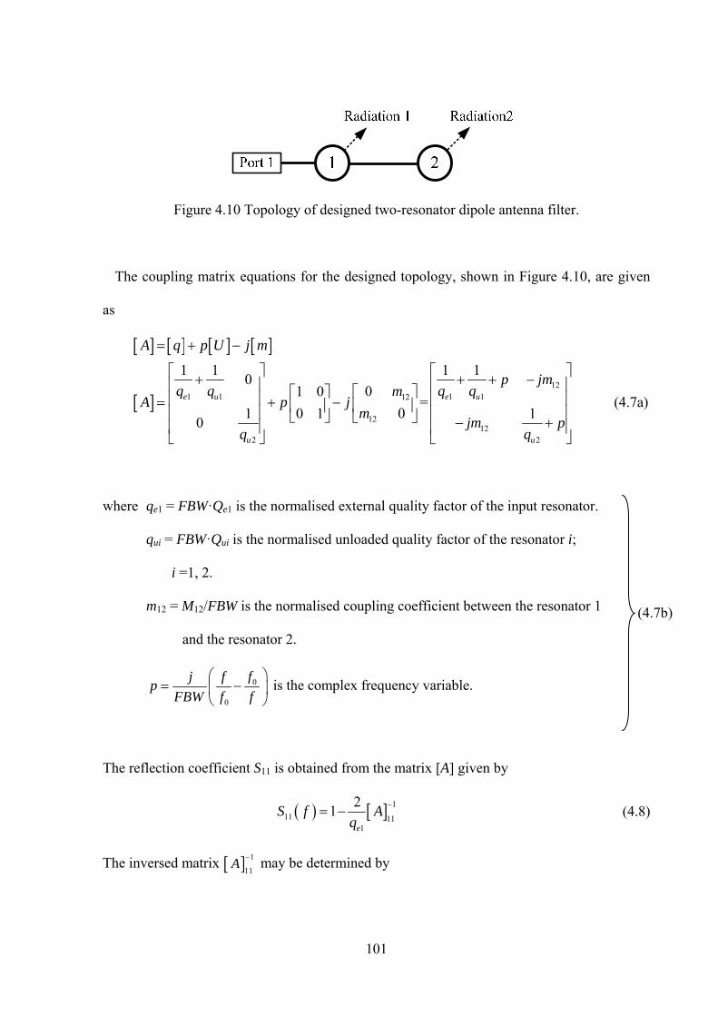
101
(4.7b)
Figure 4.10 Topology of designed two-resonator dipole antenna filter.
The coupling matrix equations for the designed topology, shown in Figure 4.10, are given
as
12
1 1 1 112
1212
2 2
1 1 1 10
01 0= (4.7a)
01 0 1 10
e u e u
u u
A q p U j m
p jmq q q qm
A p jm
jm pq q
where qe1 = FBW·Qe1 is the normalised external quality factor of the input resonator.
qui = FBW·Qui is the normalised unloaded quality factor of the resonator i;
i =1, 2.
m12 = M12/FBW is the normalised coupling coefficient between the resonator 1
and the resonator 2.
0
0
fj fp
FBW f f
is the complex frequency variable.
The reflection coefficient S11 is obtained from the matrix [A] given by
1
11 111
21
e
S f Aq
(4.8)
The inversed matrix 1
11A
may be determined by
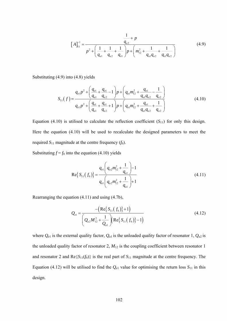
102
1 211
2 212
1 2 1 1 2 1 2
1
1 1 1 1 1u
u u e u u e u
pq
A
p p mq q q q q q q
(4.9)
Substituting (4.9) into (4.8) yields
2 21 1 1
1 1 121 2 1 2 2
112 21 1 1
1 1 121 2 1 2 2
11
11
e e ee e
u u u u u
e e ee e
u u u u u
q q qq p p q m
q q q q qS f
q q qq p p q m
q q q q q
(4.10)
Equation (4.10) is utilised to calculate the reflection coefficient (S11) for only this design.
Here the equation (4.10) will be used to recalculate the designed parameters to meet the
required S11 magnitude at the centre frequency (f0).
Substituting f = f0 into the equation (4.10) yields
2
1 2 121
11 02
1 2 121
11
Re 1
1
e uu
e uu
q q mq
S f
q q mq
(4.11)
Rearranging the equation (4.11) and using (4.7b),
11 0
12
2 12 11 01
Re 1
1Re 1
e
uu
S fQ
Q M S fQ
(4.12)
where Qe1 is the external quality factor, Qu1 is the unloaded quality factor of resonator 1, Qu2 is
the unloaded quality factor of resonator 2, M12 is the coupling coefficient between resonator 1
and resonator 2 and Re{S11(f0)} is the real part of S11 magnitude at the centre frequency. The
Equation (4.12) will be utilised to find the Qe1 value for optimising the return loss S11 in this
design.
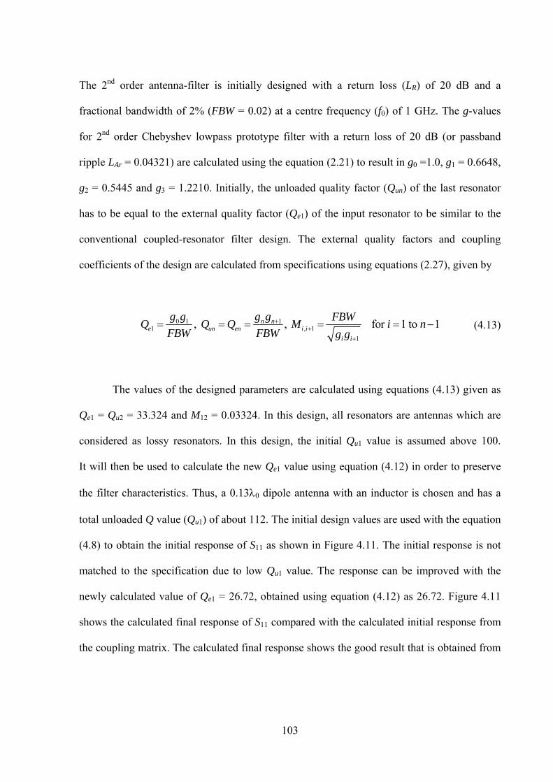
103
The 2nd order antenna-filter is initially designed with a return loss (LR) of 20 dB and a
fractional bandwidth of 2% (FBW = 0.02) at a centre frequency (f0) of 1 GHz. The g-values
for 2nd order Chebyshev lowpass prototype filter with a return loss of 20 dB (or passband
ripple LAr = 0.04321) are calculated using the equation (2.21) to result in g0 =1.0, g1 = 0.6648,
g2 = 0.5445 and g3 = 1.2210. Initially, the unloaded quality factor (Qun) of the last resonator
has to be equal to the external quality factor (Qe1) of the input resonator to be similar to the
conventional coupled-resonator filter design. The external quality factors and coupling
coefficients of the design are calculated from specifications using equations (2.27), given by
0 1 11 , 1
1
, , for 1 to 1n ne un en i i
i i
g g g g FBWQ Q Q M i n
FBW FBW g g
(4.13)
The values of the designed parameters are calculated using equations (4.13) given as
Qe1 = Qu2 = 33.324 and M12 = 0.03324. In this design, all resonators are antennas which are
considered as lossy resonators. In this design, the initial Qu1 value is assumed above 100.
It will then be used to calculate the new Qe1 value using equation (4.12) in order to preserve
the filter characteristics. Thus, a 0.130 dipole antenna with an inductor is chosen and has a
total unloaded Q value (Qu1) of about 112. The initial design values are used with the equation
(4.8) to obtain the initial response of S11 as shown in Figure 4.11. The initial response is not
matched to the specification due to low Qu1 value. The response can be improved with the
newly calculated value of Qe1 = 26.72, obtained using equation (4.12) as 26.72. Figure 4.11
shows the calculated final response of S11 compared with the calculated initial response from
the coupling matrix. The calculated final response shows the good result that is obtained from
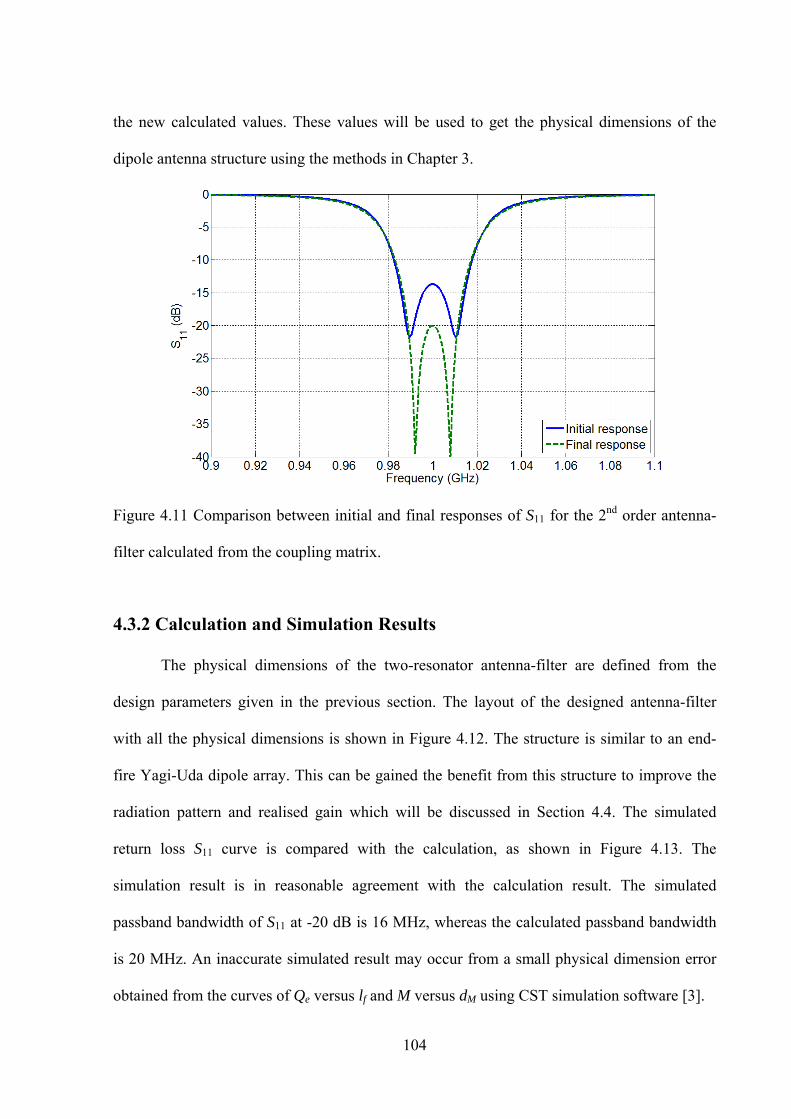
104
the new calculated values. These values will be used to get the physical dimensions of the
dipole antenna structure using the methods in Chapter 3.
Figure 4.11 Comparison between initial and final responses of S11 for the 2nd order antenna-
filter calculated from the coupling matrix.
4.3.2 Calculation and Simulation Results
The physical dimensions of the two-resonator antenna-filter are defined from the
design parameters given in the previous section. The layout of the designed antenna-filter
with all the physical dimensions is shown in Figure 4.12. The structure is similar to an end-
fire Yagi-Uda dipole array. This can be gained the benefit from this structure to improve the
radiation pattern and realised gain which will be discussed in Section 4.4. The simulated
return loss S11 curve is compared with the calculation, as shown in Figure 4.13. The
simulation result is in reasonable agreement with the calculation result. The simulated
passband bandwidth of S11 at -20 dB is 16 MHz, whereas the calculated passband bandwidth
is 20 MHz. An inaccurate simulated result may occur from a small physical dimension error
obtained from the curves of Qe versus lf and M versus dM using CST simulation software [3].
105
Figure 4.12 Geometry of 2nd order dipole antenna filter are a = 0.75 mm, g = 5mm, l1 = 16.1
mm, l2 = 17 mm, l3 = 32.75 mm, d1 = 2.5 mm, d2 = 21.3 mm.
Figure 4.13 Calculated and simulated response of S11 of 2nd order dipole antenna-filter.
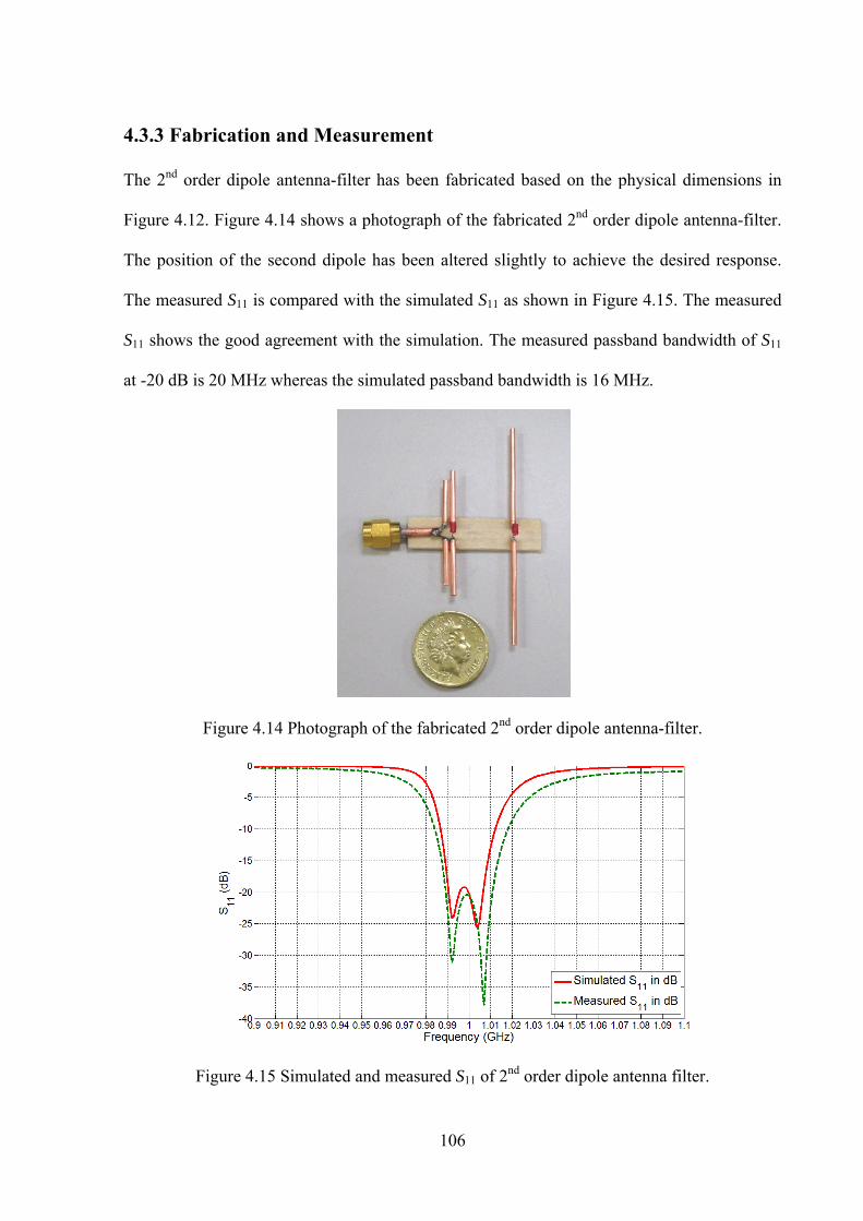
4.3.3
The
Figur
The
The m
S11 s
at -20
3 Fabrica
2nd order d
re 4.12. Fig
position of
measured S
hows the g
0 dB is 20 M
Figu
Figure
ation and
dipole anten
gure 4.14 sh
f the second
S11 is compa
ood agreem
MHz where
ure 4.14 Pho
e 4.15 Simu
Measurem
nna-filter ha
hows a phot
d dipole has
ared with th
ment with th
eas the simu
otograph of
ulated and m
106
ment
as been fabr
tograph of t
s been alter
he simulated
he simulatio
ulated passb
the fabricat
measured S1
ricated base
the fabricat
red slightly
d S11 as sho
on. The mea
and bandwi
ted 2nd orde
11 of 2nd ord
ed on the p
ed 2nd order
y to achieve
own in Figu
asured passb
idth is 16 M
r dipole ant
der dipole an
physical dim
r dipole ant
e the desired
ure 4.15. Th
band bandw
MHz.
tenna-filter.
ntenna filter
mensions in
tenna-filter.
d response.
e measured
width of S11
r.
n
.
.
d
1
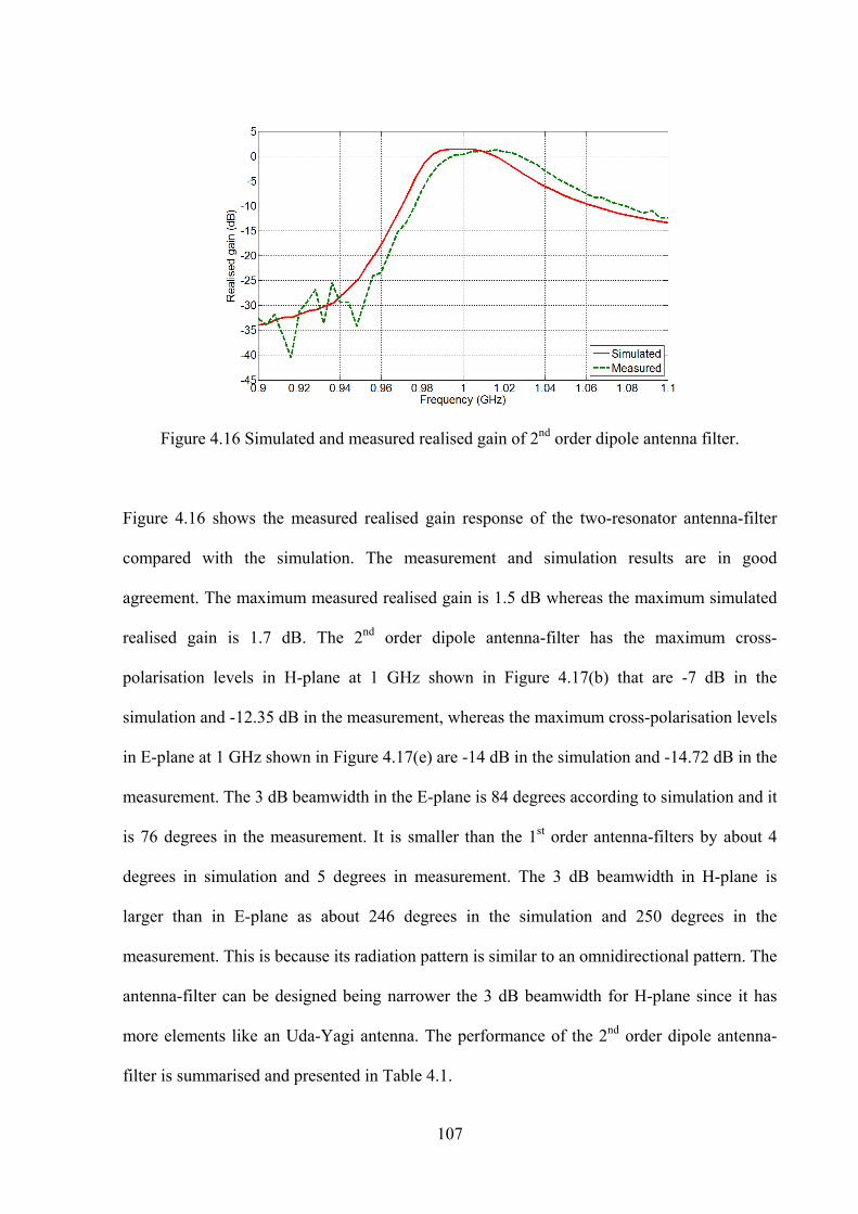
107
Figure 4.16 Simulated and measured realised gain of 2nd order dipole antenna filter.
Figure 4.16 shows the measured realised gain response of the two-resonator antenna-filter
compared with the simulation. The measurement and simulation results are in good
agreement. The maximum measured realised gain is 1.5 dB whereas the maximum simulated
realised gain is 1.7 dB. The 2nd order dipole antenna-filter has the maximum cross-
polarisation levels in H-plane at 1 GHz shown in Figure 4.17(b) that are -7 dB in the
simulation and -12.35 dB in the measurement, whereas the maximum cross-polarisation levels
in E-plane at 1 GHz shown in Figure 4.17(e) are -14 dB in the simulation and -14.72 dB in the
measurement. The 3 dB beamwidth in the E-plane is 84 degrees according to simulation and it
is 76 degrees in the measurement. It is smaller than the 1st order antenna-filters by about 4
degrees in simulation and 5 degrees in measurement. The 3 dB beamwidth in H-plane is
larger than in E-plane as about 246 degrees in the simulation and 250 degrees in the
measurement. This is because its radiation pattern is similar to an omnidirectional pattern. The
antenna-filter can be designed being narrower the 3 dB beamwidth for H-plane since it has
more elements like an Uda-Yagi antenna. The performance of the 2nd order dipole antenna-
filter is summarised and presented in Table 4.1.
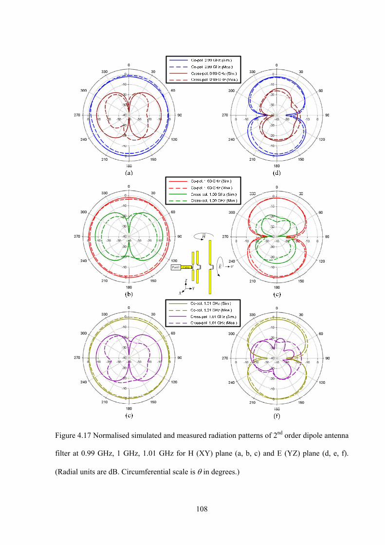
108
0o
H
E
Z
XY
Port1 Cable
Figure 4.17 Normalised simulated and measured radiation patterns of 2nd order dipole antenna
filter at 0.99 GHz, 1 GHz, 1.01 GHz for H (XY) plane (a, b, c) and E (YZ) plane (d, e, f).
(Radial units are dB. Circumferential scale is in degrees.)
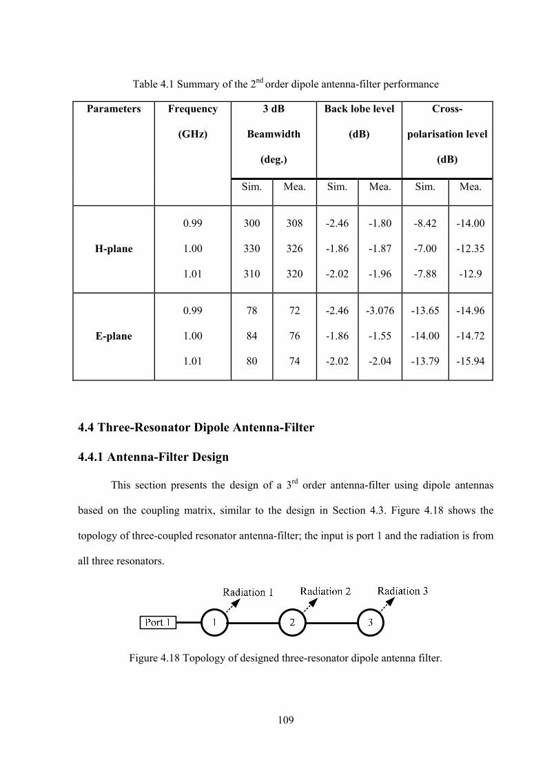
109
Table 4.1 Summary of the 2nd order dipole antenna-filter performance
Parameters Frequency
(GHz)
3 dB
Beamwidth
(deg.)
Back lobe level
(dB)
Cross-
polarisation level
(dB)
Sim. Mea. Sim. Mea. Sim. Mea.
H-plane
0.99
1.00
1.01
300
330
310
308
326
320
-2.46
-1.86
-2.02
-1.80
-1.87
-1.96
-8.42
-7.00
-7.88
-14.00
-12.35
-12.9
E-plane
0.99
1.00
1.01
78
84
80
72
76
74
-2.46
-1.86
-2.02
-3.076
-1.55
-2.04
-13.65
-14.00
-13.79
-14.96
-14.72
-15.94
4.4 Three-Resonator Dipole Antenna-Filter
4.4.1 Antenna-Filter Design
This section presents the design of a 3rd order antenna-filter using dipole antennas
based on the coupling matrix, similar to the design in Section 4.3. Figure 4.18 shows the
topology of three-coupled resonator antenna-filter; the input is port 1 and the radiation is from
all three resonators.
Figure 4.18 Topology of designed three-resonator dipole antenna filter.
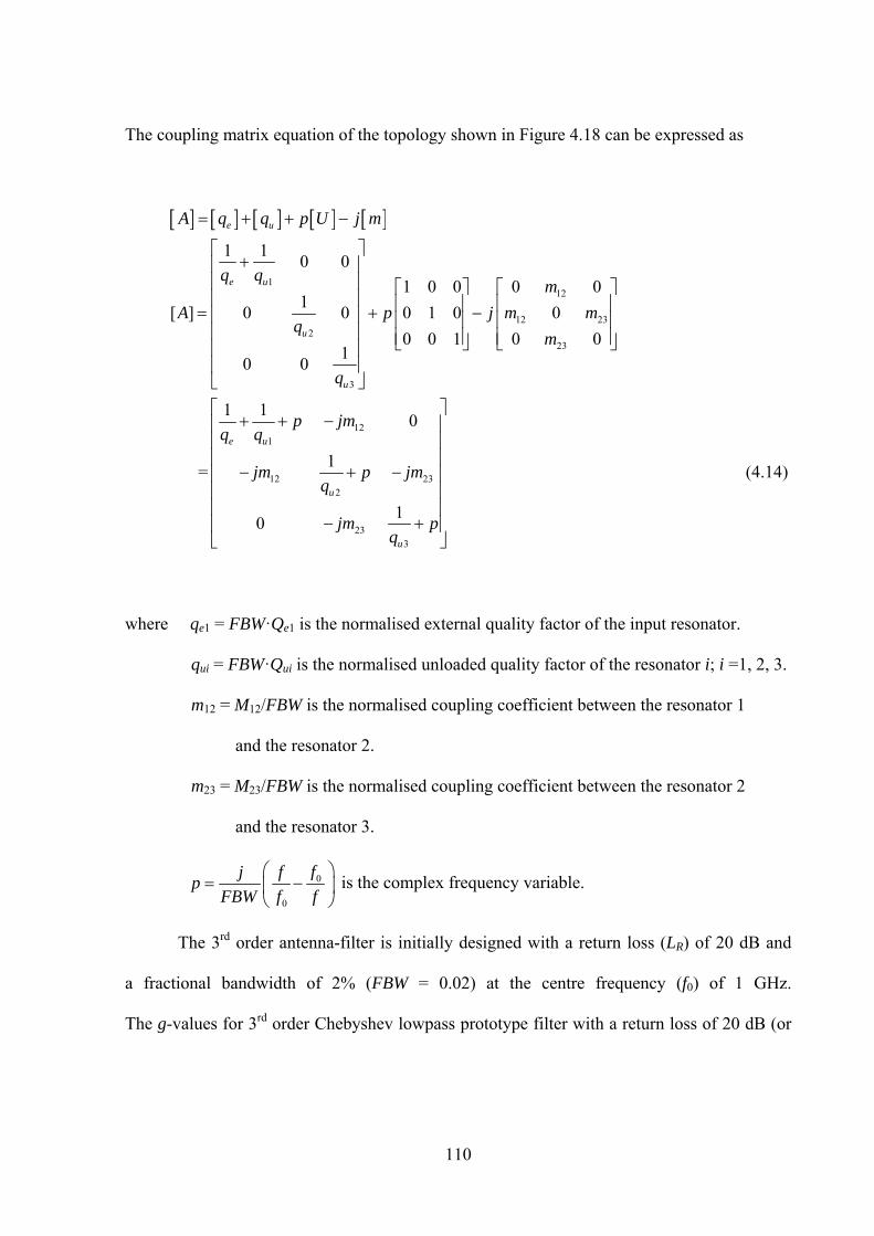
110
The coupling matrix equation of the topology shown in Figure 4.18 can be expressed as
112
12 232
23
3
121
12 232
233
1 10 0
1 0 0 0 01
[ ] 0 0 0 1 0 0
0 0 1 0 01
0 0
1 10
1 =
10
e u
e u
u
u
e u
u
u
A q q p U j m
q qm
A p j m mq
m
q
p jmq q
jm p jmq
jm pq
(4.14)
where qe1 = FBW·Qe1 is the normalised external quality factor of the input resonator.
qui = FBW·Qui is the normalised unloaded quality factor of the resonator i; i =1, 2, 3.
m12 = M12/FBW is the normalised coupling coefficient between the resonator 1
and the resonator 2.
m23 = M23/FBW is the normalised coupling coefficient between the resonator 2
and the resonator 3.
0
0
fj fp
FBW f f
is the complex frequency variable.
The 3rd order antenna-filter is initially designed with a return loss (LR) of 20 dB and
a fractional bandwidth of 2% (FBW = 0.02) at the centre frequency (f0) of 1 GHz.
The g-values for 3rd order Chebyshev lowpass prototype filter with a return loss of 20 dB (or
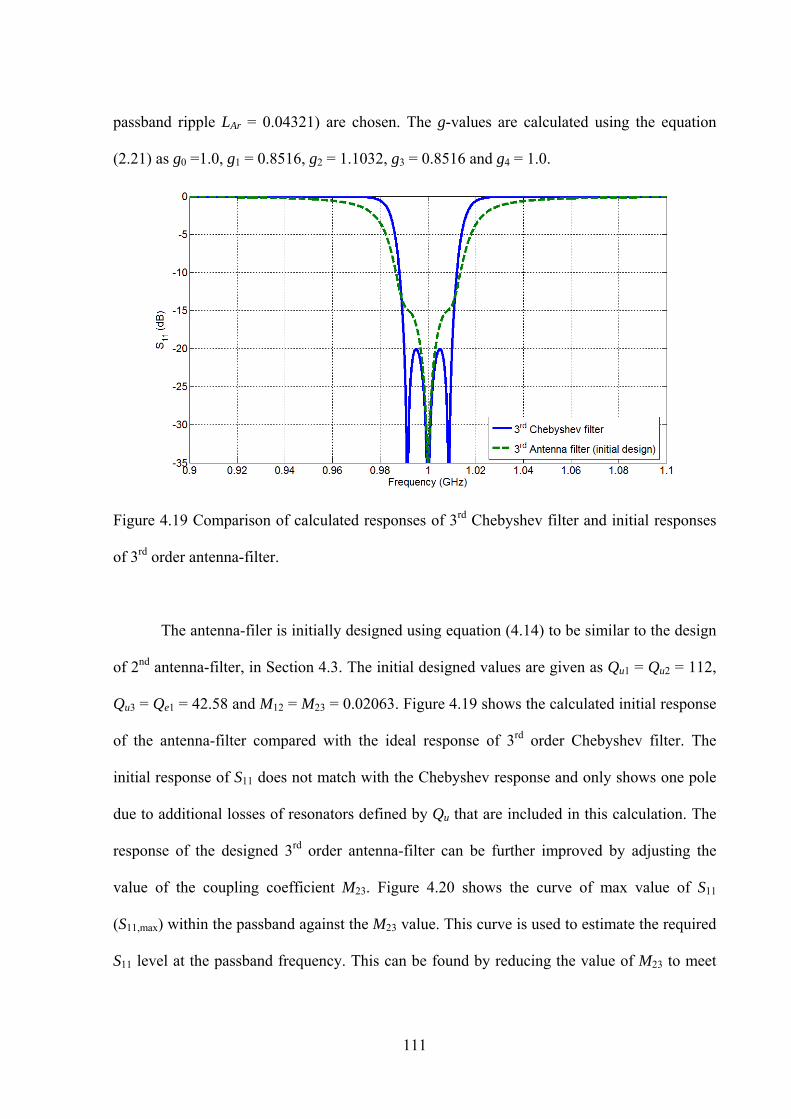
111
passband ripple LAr = 0.04321) are chosen. The g-values are calculated using the equation
(2.21) as g0 =1.0, g1 = 0.8516, g2 = 1.1032, g3 = 0.8516 and g4 = 1.0.
Figure 4.19 Comparison of calculated responses of 3rd Chebyshev filter and initial responses
of 3rd order antenna-filter.
The antenna-filer is initially designed using equation (4.14) to be similar to the design
of 2nd antenna-filter, in Section 4.3. The initial designed values are given as Qu1 = Qu2 = 112,
Qu3 = Qe1 = 42.58 and M12 = M23 = 0.02063. Figure 4.19 shows the calculated initial response
of the antenna-filter compared with the ideal response of 3rd order Chebyshev filter. The
initial response of S11 does not match with the Chebyshev response and only shows one pole
due to additional losses of resonators defined by Qu that are included in this calculation. The
response of the designed 3rd order antenna-filter can be further improved by adjusting the
value of the coupling coefficient M23. Figure 4.20 shows the curve of max value of S11
(S11,max) within the passband against the M23 value. This curve is used to estimate the required
S11 level at the passband frequency. This can be found by reducing the value of M23 to meet
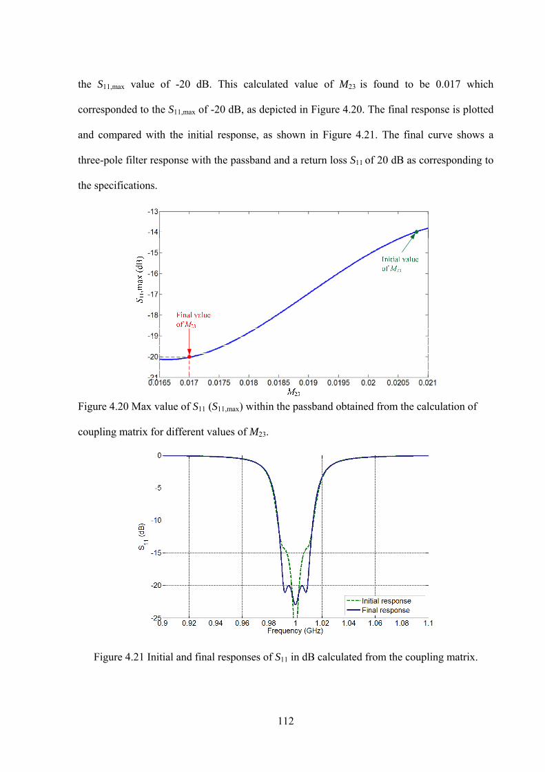
112
the S11,max value of -20 dB. This calculated value of M23 is found to be 0.017 which
corresponded to the S11,max of -20 dB, as depicted in Figure 4.20. The final response is plotted
and compared with the initial response, as shown in Figure 4.21. The final curve shows a
three-pole filter response with the passband and a return loss S11 of 20 dB as corresponding to
the specifications.
Figure 4.20 Max value of S11 (S11,max) within the passband obtained from the calculation of
coupling matrix for different values of M23.
Figure 4.21 Initial and final responses of S11 in dB calculated from the coupling matrix.
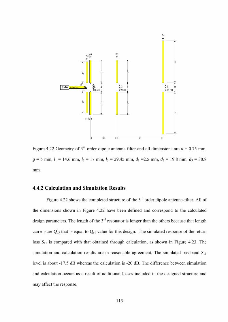
113
SMA L1
68 nHg
2a2a
l2
l2
l1
l1
gRG405/U
d1
d2
L3
54 nHg
l3
l3
2a
L2
93nHg
2a
l2
l2
d3
Figure 4.22 Geometry of 3rd order dipole antenna filter and all dimensions are a = 0.75 mm,
g = 5 mm, l1 = 14.6 mm, l2 = 17 mm, l3 = 29.45 mm, d1 =2.5 mm, d2 = 19.8 mm, d3 = 30.8
mm.
4.4.2 Calculation and Simulation Results
Figure 4.22 shows the completed structure of the 3rd order dipole antenna-filter. All of
the dimensions shown in Figure 4.22 have been defined and correspond to the calculated
design parameters. The length of the 3rd resonator is longer than the others because that length
can ensure Qu3 that is equal to Qe1 value for this design. The simulated response of the return
loss S11 is compared with that obtained through calculation, as shown in Figure 4.23. The
simulation and calculation results are in reasonable agreement. The simulated passband S11
level is about -17.5 dB whereas the calculation is -20 dB. The difference between simulation
and calculation occurs as a result of additional losses included in the designed structure and
may affect the response.
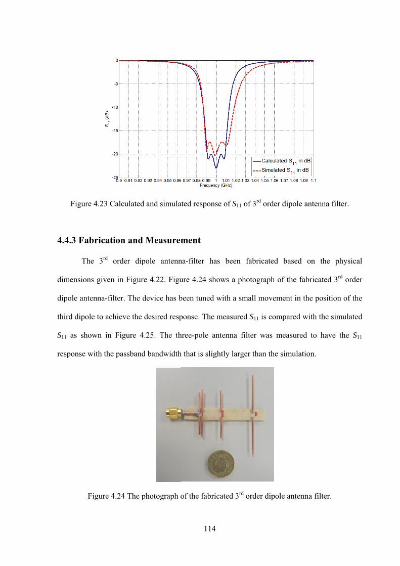
F
4.4.3
dime
dipol
third
S11 a
respo
Figure 4.23
3 Fabrica
The 3rd
ensions give
le antenna-f
d dipole to a
as shown in
onse with th
Figure
Calculated
ation and
order dip
en in Figure
filter. The d
achieve the d
n Figure 4.
he passband
e 4.24 The p
and simula
Measurem
pole antenn
e 4.22. Figu
device has b
desired resp
.25. The th
d bandwidth
photograph o
114
ated respons
ment
na-filter ha
ure 4.24 sho
been tuned w
ponse. The m
hree-pole an
h that is slig
of the fabric
se of S11 of 3
as been fab
ows a photo
with a smal
measured S
ntenna filte
htly larger t
cated 3rd ord
3rd order dip
bricated ba
ograph of th
ll movemen
S11 is compa
er was mea
than the sim
der dipole a
pole antenn
ased on th
he fabricate
nt in the pos
ared with th
asured to ha
mulation.
antenna filte
na filter.
he physical
ed 3rd order
sition of the
e simulated
ave the S11
er.
l
r
e
d
1
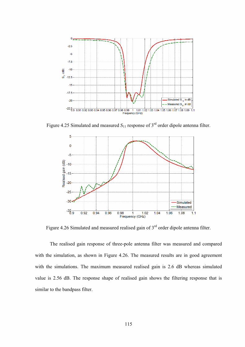
115
Figure 4.25 Simulated and measured S11 response of 3rd order dipole antenna filter.
Figure 4.26 Simulated and measured realised gain of 3rd order dipole antenna filter.
The realised gain response of three-pole antenna filter was measured and compared
with the simulation, as shown in Figure 4.26. The measured results are in good agreement
with the simulations. The maximum measured realised gain is 2.6 dB whereas simulated
value is 2.56 dB. The response shape of realised gain shows the filtering response that is
similar to the bandpass filter.
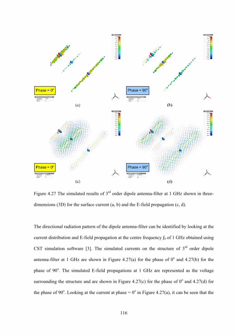
116
Figure 4.27 The simulated results of 3rd order dipole antenna-filter at 1 GHz shown in three-
dimensions (3D) for the surface current (a, b) and the E-field propagation (c, d).
The directional radiation pattern of the dipole antenna-filter can be identified by looking at the
current distribution and E-field propagation at the centre frequency f0 of 1 GHz obtained using
CST simulation software [3]. The simulated currents on the structure of 3rd order dipole
antenna-filter at 1 GHz are shown in Figure 4.27(a) for the phase of 0o and 4.27(b) for the
phase of 90o. The simulated E-field propagations at 1 GHz are represented as the voltage
surrounding the structure and are shown in Figure 4.27(c) for the phase of 0o and 4.27(d) for
the phase of 90o. Looking at the current at phase = 0o in Figure 4.27(a), it can be seen that the
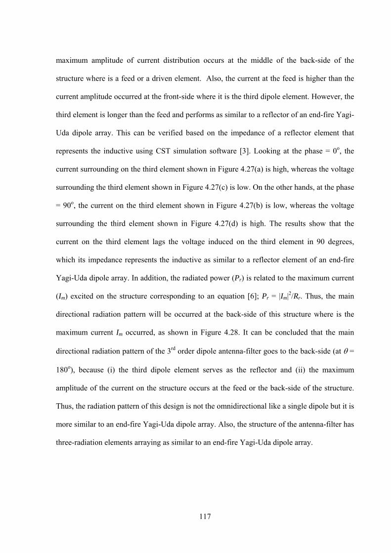
117
maximum amplitude of current distribution occurs at the middle of the back-side of the
structure where is a feed or a driven element. Also, the current at the feed is higher than the
current amplitude occurred at the front-side where it is the third dipole element. However, the
third element is longer than the feed and performs as similar to a reflector of an end-fire Yagi-
Uda dipole array. This can be verified based on the impedance of a reflector element that
represents the inductive using CST simulation software [3]. Looking at the phase = 0o, the
current surrounding on the third element shown in Figure 4.27(a) is high, whereas the voltage
surrounding the third element shown in Figure 4.27(c) is low. On the other hands, at the phase
= 90o, the current on the third element shown in Figure 4.27(b) is low, whereas the voltage
surrounding the third element shown in Figure 4.27(d) is high. The results show that the
current on the third element lags the voltage induced on the third element in 90 degrees,
which its impedance represents the inductive as similar to a reflector element of an end-fire
Yagi-Uda dipole array. In addition, the radiated power (Pr) is related to the maximum current
(Im) excited on the structure corresponding to an equation [6]; Pr = |Im|2/Rr. Thus, the main
directional radiation pattern will be occurred at the back-side of this structure where is the
maximum current Im occurred, as shown in Figure 4.28. It can be concluded that the main
directional radiation pattern of the 3rd order dipole antenna-filter goes to the back-side (at =
180o), because (i) the third dipole element serves as the reflector and (ii) the maximum
amplitude of the current on the structure occurs at the feed or the back-side of the structure.
Thus, the radiation pattern of this design is not the omnidirectional like a single dipole but it is
more similar to an end-fire Yagi-Uda dipole array. Also, the structure of the antenna-filter has
three-radiation elements arraying as similar to an end-fire Yagi-Uda dipole array.
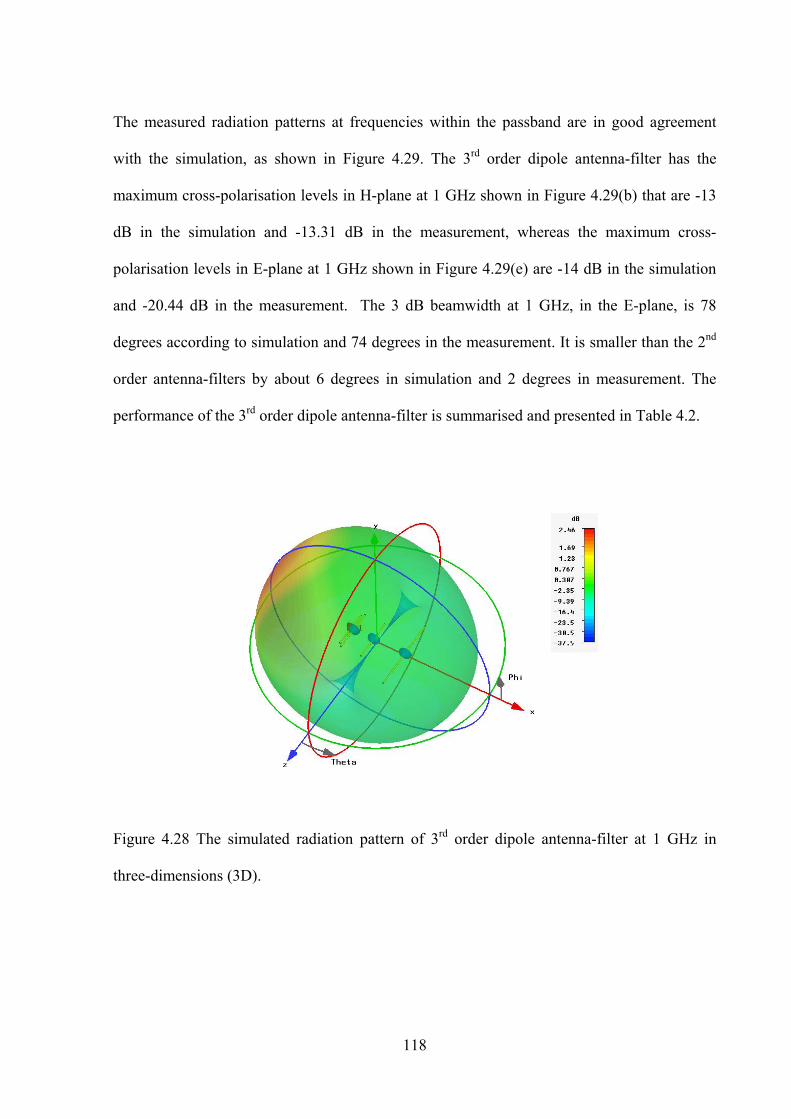
118
The measured radiation patterns at frequencies within the passband are in good agreement
with the simulation, as shown in Figure 4.29. The 3rd order dipole antenna-filter has the
maximum cross-polarisation levels in H-plane at 1 GHz shown in Figure 4.29(b) that are -13
dB in the simulation and -13.31 dB in the measurement, whereas the maximum cross-
polarisation levels in E-plane at 1 GHz shown in Figure 4.29(e) are -14 dB in the simulation
and -20.44 dB in the measurement. The 3 dB beamwidth at 1 GHz, in the E-plane, is 78
degrees according to simulation and 74 degrees in the measurement. It is smaller than the 2nd
order antenna-filters by about 6 degrees in simulation and 2 degrees in measurement. The
performance of the 3rd order dipole antenna-filter is summarised and presented in Table 4.2.
Figure 4.28 The simulated radiation pattern of 3rd order dipole antenna-filter at 1 GHz in
three-dimensions (3D).
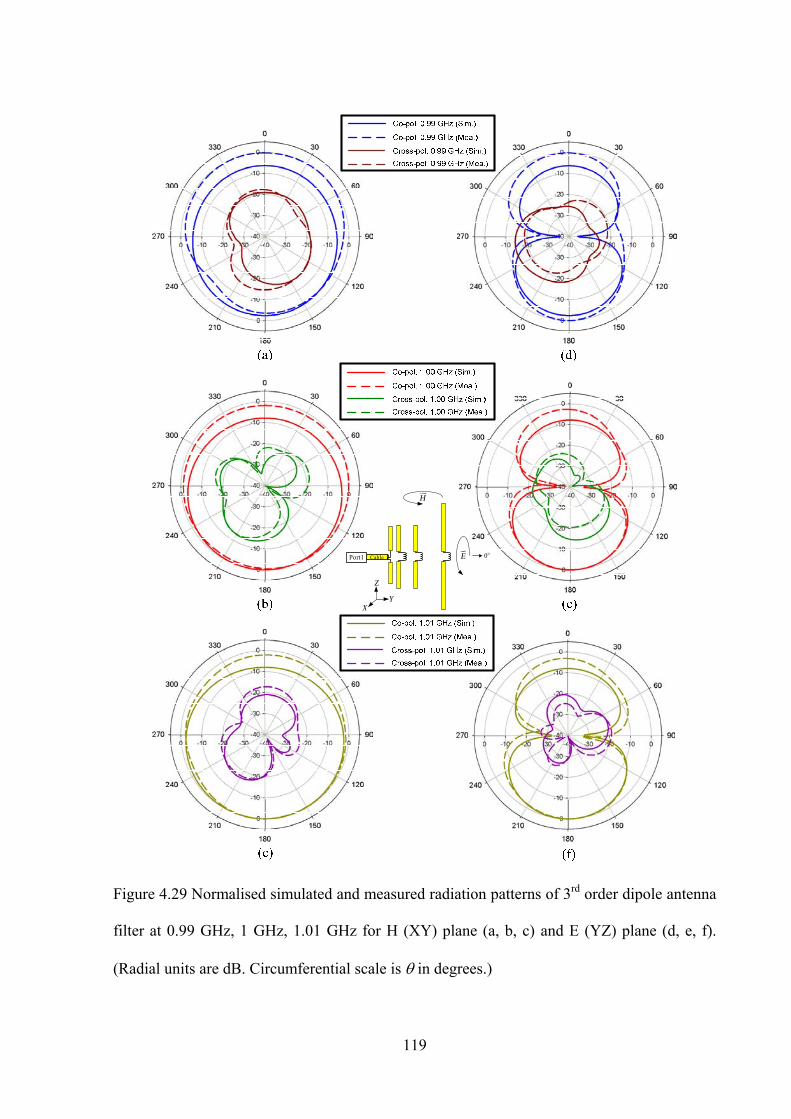
119
0o
H
E
Z
XY
Port1 Cable
Figure 4.29 Normalised simulated and measured radiation patterns of 3rd order dipole antenna
filter at 0.99 GHz, 1 GHz, 1.01 GHz for H (XY) plane (a, b, c) and E (YZ) plane (d, e, f).
(Radial units are dB. Circumferential scale is in degrees.)
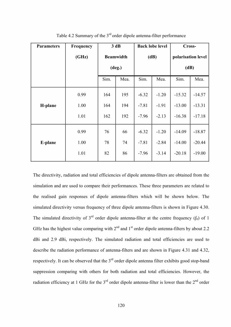
120
Table 4.2 Summary of the 3rd order dipole antenna-filter performance
Parameters Frequency
(GHz)
3 dB
Beamwidth
(deg.)
Back lobe level
(dB)
Cross-
polarisation level
(dB)
Sim. Mea. Sim. Mea. Sim. Mea.
H-plane
0.99
1.00
1.01
164
164
162
195
194
192
-6.32
-7.81
-7.96
-1.20
-1.91
-2.13
-15.32
-13.00
-16.38
-14.57
-13.31
-17.18
E-plane
0.99
1.00
1.01
76
78
82
66
74
86
-6.32
-7.81
-7.96
-1.20
-2.84
-3.14
-14.09
-14.00
-20.18
-18.87
-20.44
-19.00
The directivity, radiation and total efficiencies of dipole antenna-filters are obtained from the
simulation and are used to compare their performances. These three parameters are related to
the realised gain responses of dipole antenna-filters which will be shown below. The
simulated directivity versus frequency of three dipole antenna-filters is shown in Figure 4.30.
The simulated directivity of 3rd order dipole antenna-filter at the centre frequency (f0) of 1
GHz has the highest value comparing with 2nd and 1st order dipole antenna-filters by about 2.2
dBi and 2.9 dBi, respectively. The simulated radiation and total efficiencies are used to
describe the radiation performance of antenna-filters and are shown in Figure 4.31 and 4.32,
respectively. It can be observed that the 3rd order dipole antenna filter exhibits good stop-band
suppression comparing with others for both radiation and total efficiencies. However, the
radiation efficiency at 1 GHz for the 3rd order dipole antenna-filter is lower than the 2nd order
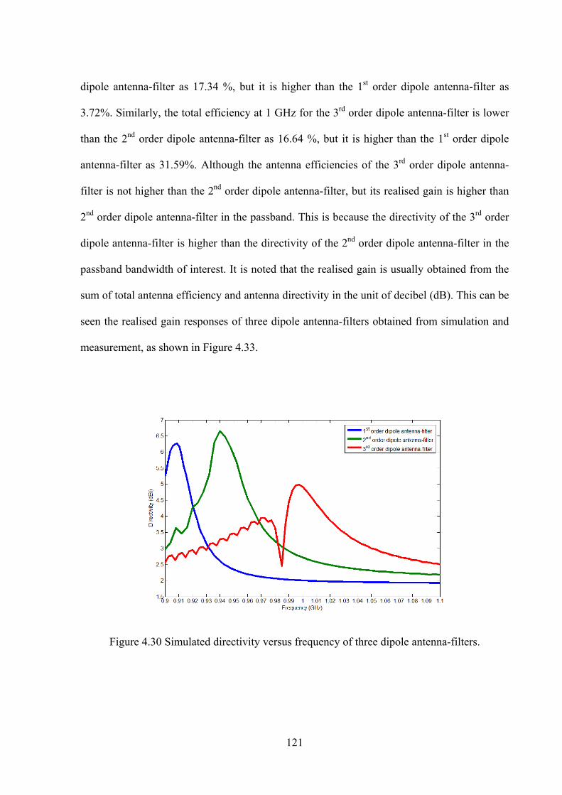
121
dipole antenna-filter as 17.34 %, but it is higher than the 1st order dipole antenna-filter as
3.72%. Similarly, the total efficiency at 1 GHz for the 3rd order dipole antenna-filter is lower
than the 2nd order dipole antenna-filter as 16.64 %, but it is higher than the 1st order dipole
antenna-filter as 31.59%. Although the antenna efficiencies of the 3rd order dipole antenna-
filter is not higher than the 2nd order dipole antenna-filter, but its realised gain is higher than
2nd order dipole antenna-filter in the passband. This is because the directivity of the 3rd order
dipole antenna-filter is higher than the directivity of the 2nd order dipole antenna-filter in the
passband bandwidth of interest. It is noted that the realised gain is usually obtained from the
sum of total antenna efficiency and antenna directivity in the unit of decibel (dB). This can be
seen the realised gain responses of three dipole antenna-filters obtained from simulation and
measurement, as shown in Figure 4.33.
Figure 4.30 Simulated directivity versus frequency of three dipole antenna-filters.
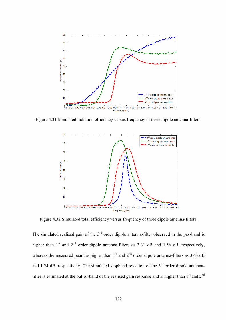
122
Figure 4.31 Simulated radiation efficiency versus frequency of three dipole antenna-filters.
Figure 4.32 Simulated total efficiency versus frequency of three dipole antenna-filters.
The simulated realised gain of the 3rd order dipole antenna-filter observed in the passband is
higher than 1st and 2nd order dipole antenna-filters as 3.31 dB and 1.56 dB, respectively,
whereas the measured result is higher than 1st and 2nd order dipole antenna-filters as 3.63 dB
and 1.24 dB, respectively. The simulated stopband rejection of the 3rd order dipole antenna-
filter is estimated at the out-of-band of the realised gain response and is higher than 1st and 2nd
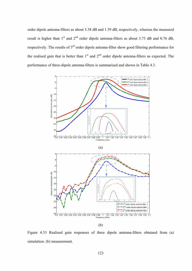
123
order dipole antenna-filters as about 3.38 dB and 1.39 dB, respectively, whereas the measured
result is higher than 1st and 2nd order dipole antenna-filters as about 3.73 dB and 0.76 dB,
respectively. The results of 3rd order dipole antenna-filter show good filtering performance for
the realised gain that is better than 1st and 2nd order dipole antenna-filters as expected. The
performance of three-dipole antenna-filters is summarised and shown in Table 4.3.
(a)
(b)
Figure 4.33 Realised gain responses of three dipole antenna-filters obtained from (a)
simulation. (b) measurement.
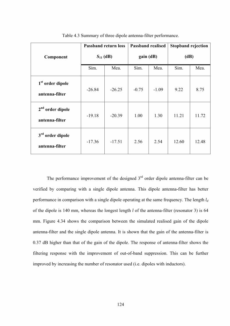
124
Table 4.3 Summary of three dipole antenna-filter performance.
Component
Passband return loss
S11 (dB)
Passband realised
gain (dB)
Stopband rejection
(dB)
Sim. Mea. Sim. Mea. Sim. Mea.
1st order dipole
antenna-filter
-26.84
-26.25
-0.75
-1.09
9.22
8.75
2nd order dipole
antenna-filter
-19.18
-20.39
1.00
1.30
11.21
11.72
3rd order dipole
antenna-filter
-17.36
-17.51
2.56
2.54
12.60
12.48
The performance improvement of the designed 3rd order dipole antenna-filter can be
verified by comparing with a single dipole antenna. This dipole antenna-filter has better
performance in comparison with a single dipole operating at the same frequency. The length ld
of the dipole is 140 mm, whereas the longest length l of the antenna-filter (resonator 3) is 64
mm. Figure 4.34 shows the comparison between the simulated realised gain of the dipole
antenna-filter and the single dipole antenna. It is shown that the gain of the antenna-filter is
0.37 dB higher than that of the gain of the dipole. The response of antenna-filter shows the
filtering response with the improvement of out-of-band suppression. This can be further
improved by increasing the number of resonator used (i.e. dipoles with inductors).
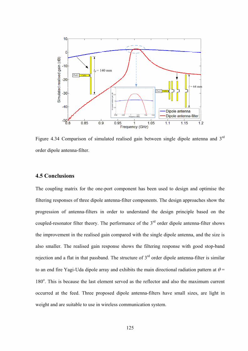
125
Port1 Cable
ld = 140 mm
Port1 Cable
l = 64 mm
Figure 4.34 Comparison of simulated realised gain between single dipole antenna and 3rd
order dipole antenna-filter.
4.5 Conclusions
The coupling matrix for the one-port component has been used to design and optimise the
filtering responses of three dipole antenna-filter components. The design approaches show the
progression of antenna-filters in order to understand the design principle based on the
coupled-resonator filter theory. The performance of the 3rd order dipole antenna-filter shows
the improvement in the realised gain compared with the single dipole antenna, and the size is
also smaller. The realised gain response shows the filtering response with good stop-band
rejection and a flat in that passband. The structure of 3rd order dipole antenna-filter is similar
to an end fire Yagi-Uda dipole array and exhibits the main directional radiation pattern at =
180o. This is because the last element served as the reflector and also the maximum current
occurred at the feed. Three proposed dipole antenna-filters have small sizes, are light in
weight and are suitable to use in wireless communication system.
126
References
[1] Hong J. S. and Lancaster M. J. Microstrip Filters for RF/Microwave Applications. New
York, USA: John Wiley & Sons; 2001.
[2] Cameron R. J., Kudsia C. M. And Mansour R. R. Microwave Filters for Communication
Systems: Fundamental, Design, and Applications. New Jersey, USA: John Wiley & Sons;
2007.
[3] Computer Simulation Technology (CST), Microwave Studio [Internet]. 2014 Available
from URL: http://www.cst.com.
[4] Lancaster M. J. Passive Microwave Device Applications of High-Temperature
Superconductors. Cambridge, UK: Cambridge University Press; 1997.
[5] Kraus J. D. and Marhefka R. J. Antennas For All Applications. 3rd ed. New York, USA:
McGraw-Hill; 2003.
[6] Balanis C. A. Antenna Theory Analysis and Design. 3rd ed. New Jersey, USA: John
Wiley & Sons; 2005.
127
Chapter 5
Waveguide Antenna-Filters
5.1 Introduction
Chapter 4 presented design methodology for a one-port dipole antenna-filter. This
methodology involved using the coupling matrix for lossy resonator circuits, to optimise
return loss (S11) of low Qu resonators. In general, all resonators in the filter circuit require a
high unloaded quality factor in order to improve the passband frequency response [1]. For
example, a rectangular waveguide cavity resonator can provide high unloaded quality factor.
The structure of a rectangular cavity [2] when enclosed has low energy loss in the resonator.
The design is simple and can be utilised to combine with other waveguide components such
as waveguide aperture antennas. This chapter presents three design approaches for X-band
waveguide aperture antennas which are integrated with the rectangular waveguide cavity
resonators. Figure 5.1(a) shows a diagram of the first design. The concept is to replace the last
resonator of the filter circuit with an antenna. In this case, the antenna can serve
simultaneously in as one of the resonators of the filter and a radiator. In addition, the approach
shown in Figure 5.1 (b) is called an antenna power divider. The principle of the filter design
is used here to combine the bandpass filter, the power divider and two-antenna array into a
single component. The third approach shown in Figure 5.1 (c), which involved integrating
with a pair of bandpass filters for splitting two frequency bands and is named an antenna-
diplexer. The three design approaches presented here may be of interest in the reduction of
sizes in comparison with the conventional designs. Coupling matrix synthesis is employed for
all three-designs. The three design approaches, mentioned above, have been fabricated. They
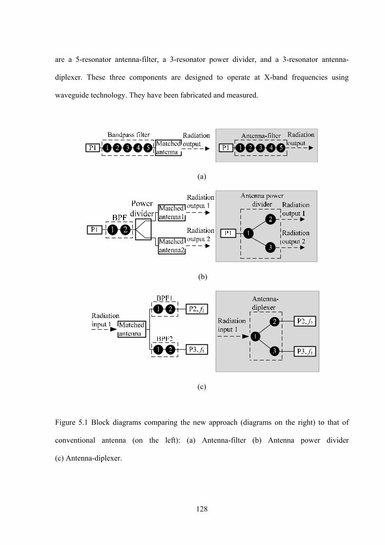
128
are a 5-resonator antenna-filter, a 3-resonator power divider, and a 3-resonator antenna-
diplexer. These three components are designed to operate at X-band frequencies using
waveguide technology. They have been fabricated and measured.
(a)
(b)
(c)
Figure 5.1 Block diagrams comparing the new approach (diagrams on the right) to that of
conventional antenna (on the left): (a) Antenna-filter (b) Antenna power divider
(c) Antenna-diplexer.
129
In this chapter, Section 5.2 presents the overview of the rectangular waveguide cavity. Section
5.3 presents the design of the waveguide aperture antenna. Section 5.4 describes the
methodology for extracting the coupling coefficient extraction from the physical structure of
waveguide components. The coupling matrix synthesis is presented in Section 5.5. The
design, simulation, fabrication and measurement of the X-band 5-resonator antenna-filter, the
X-band 3-resonator antenna power divider and the X-band 3-resonator antenna diplexer are
discussed in Section 5.6, Section 5.7 and Section 5.8, respectively. A conclusion is given in
Section 5.9.
5.2. Quality Factors of Cavity Resonators
The cavity resonator design has been described in Chapter 2. The total quality factor of a
cavity resonator coupled to an external circuit can be expressed using the loaded quality factor
(Ql), which may be defined as [3]
1 1 1
l e uQ Q Q (5.1)
where Qe is the external quality factor associated with the external coupling at the input port.
Qu is the unloaded quality factor associated with losses in the resonator.
The total Qu of the cavity resonator may be defined by adding these losses together as follows
[3]
1 1 1 1
u c d rQ Q Q Q (5.2)
where Qc, Qd and Qr are the conductor, dielectric and radiation quality factors, respectively.
For an air-filled waveguide cavity resonator, the resonator has an enclosed structure covered
with conducting material and no dielectric material within the cavity walls. It implies that the
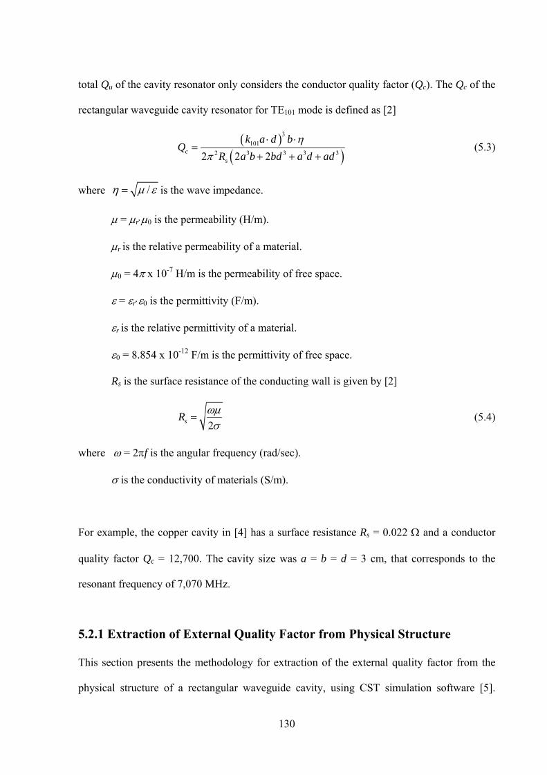
130
total Qu of the cavity resonator only considers the conductor quality factor (Qc). The Qc of the
rectangular waveguide cavity resonator for TE101 mode is defined as [2]
3
101
2 3 3 3 32 2 2c
s
k a d bQ
R a b bd a d ad
(5.3)
where / is the wave impedance.
= r0 is the permeability (H/m).
r is the relative permeability of a material.
0 = 4 x 10⁻⁷ H/m is the permeability of free space.
= r0 is the permittivity (F/m).
r is the relative permittivity of a material.
0 = 8.854 x 10⁻¹² F/m is the permittivity of free space.
Rs is the surface resistance of the conducting wall is given by [2]
2sR
(5.4)
where = 2f is the angular frequency (rad/sec).
is the conductivity of materials (S/m).
For example, the copper cavity in [4] has a surface resistance Rs = 0.022 and a conductor
quality factor Qc = 12,700. The cavity size was a = b = d = 3 cm, that corresponds to the
resonant frequency of 7,070 MHz.
5.2.1 Extraction of External Quality Factor from Physical Structure
This section presents the methodology for extraction of the external quality factor from the
physical structure of a rectangular waveguide cavity, using CST simulation software [5].
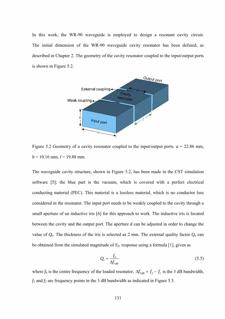
131
In this work, the WR-90 waveguide is employed to design a resonant cavity circuit.
The initial dimension of the WR-90 waveguide cavity resonator has been defined, as
described in Chapter 2. The geometry of the cavity resonator coupled to the input/output ports
is shown in Figure 5.2.
Figure 5.2 Geometry of a cavity resonator coupled to the input/output ports. a = 22.86 mm,
b = 10.16 mm, l = 19.88 mm.
The waveguide cavity structure, shown in Figure 5.2, has been made in the CST simulation
software [5]; the blue part is the vacuum, which is covered with a perfect electrical
conducting material (PEC). This material is a lossless material, which is no conductor loss
considered in the resonator. The input port needs to be weakly coupled to the cavity through a
small aperture of an inductive iris [6] for this approach to work. The inductive iris is located
between the cavity and the output port. The aperture d can be adjusted in order to change the
value of Qe. The thickness of the iris is selected as 2 mm. The external quality factor Qe can
be obtained from the simulated magnitude of S21 response using a formula [1], given as
0
3e
dB
fQ
f
(5.5)
where f0 is the centre frequency of the loaded resonator, 3 2 1dBf f f is the 3 dB bandwidth,
f1 and f2 are frequency points in the 3 dB bandwidth as indicated in Figure 5.3.
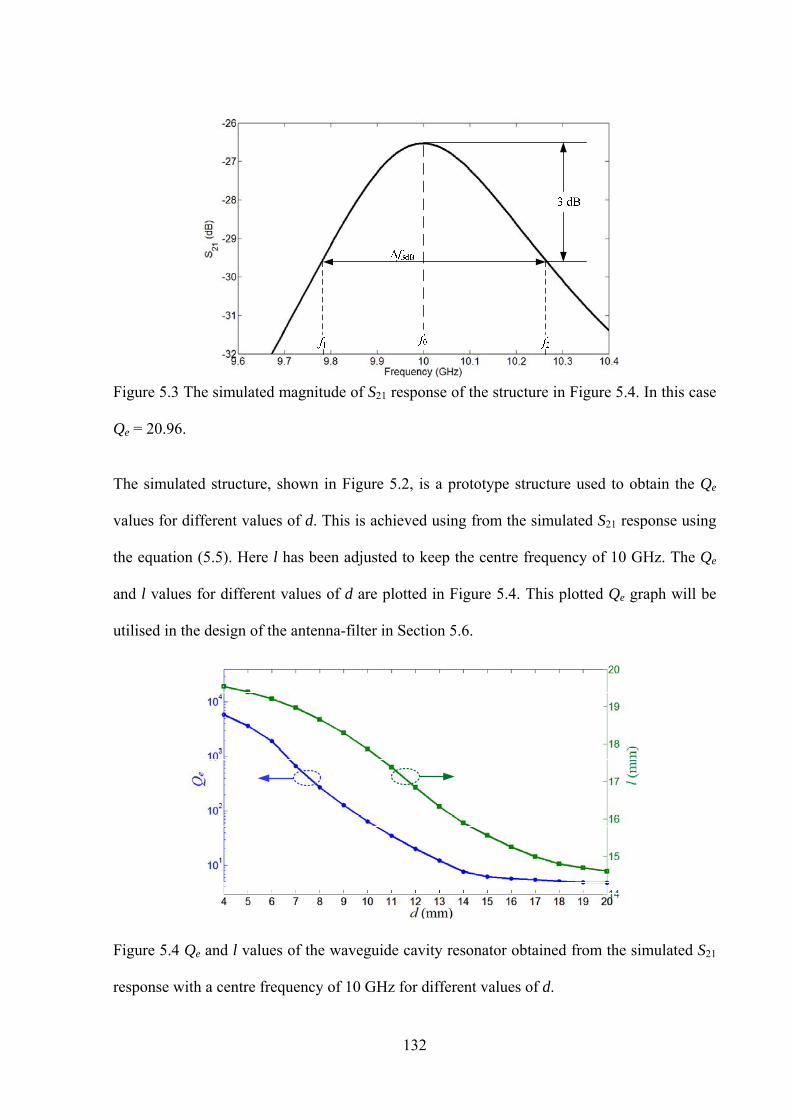
132
Figure 5.3 The simulated magnitude of S21 response of the structure in Figure 5.4. In this case
Qe = 20.96.
The simulated structure, shown in Figure 5.2, is a prototype structure used to obtain the Qe
values for different values of d. This is achieved using from the simulated S21 response using
the equation (5.5). Here l has been adjusted to keep the centre frequency of 10 GHz. The Qe
and l values for different values of d are plotted in Figure 5.4. This plotted Qe graph will be
utilised in the design of the antenna-filter in Section 5.6.
Figure 5.4 Qe and l values of the waveguide cavity resonator obtained from the simulated S21
response with a centre frequency of 10 GHz for different values of d.
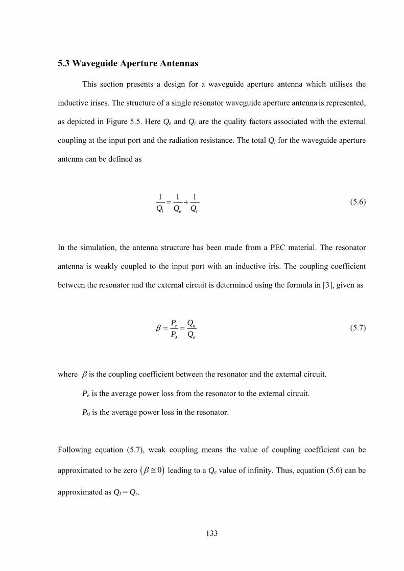
133
5.3 Waveguide Aperture Antennas
This section presents a design for a waveguide aperture antenna which utilises the
inductive irises. The structure of a single resonator waveguide aperture antenna is represented,
as depicted in Figure 5.5. Here Qe and Qr are the quality factors associated with the external
coupling at the input port and the radiation resistance. The total Ql for the waveguide aperture
antenna can be defined as
1 1 1
l e rQ Q Q (5.6)
In the simulation, the antenna structure has been made from a PEC material. The resonator
antenna is weakly coupled to the input port with an inductive iris. The coupling coefficient
between the resonator and the external circuit is determined using the formula in [3], given as
0
e u
e
P Q
P Q (5.7)
where is the coupling coefficient between the resonator and the external circuit.
Pe is the average power loss from the resonator to the external circuit.
P0 is the average power loss in the resonator.
Following equation (5.7), weak coupling means the value of coupling coefficient can be
approximated to be zero 0 leading to a Qe value of infinity. Thus, equation (5.6) can be
approximated as Ql = Qr.
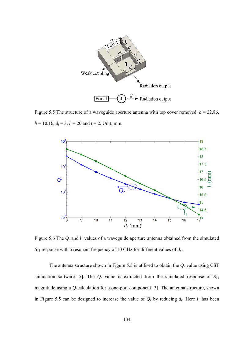
134
Figure 5.5 The structure of a waveguide aperture antenna with top cover removed. a = 22.86,
b = 10.16, di = 3, li = 20 and t = 2. Unit: mm.
dr (mm)
Qr
l1
Qr
l 1(m
m)
Figure 5.6 The Qr and l1 values of a waveguide aperture antenna obtained from the simulated
S11 response with a resonant frequency of 10 GHz for different values of dr.
The antenna structure shown in Figure 5.5 is utilised to obtain the Qr value using CST
simulation software [5]. The Qr value is extracted from the simulated response of S11
magnitude using a Q-calculation for a one-port component [3]. The antenna structure, shown
in Figure 5.5 can be designed to increase the value of Qr by reducing dr. Here l1 has been
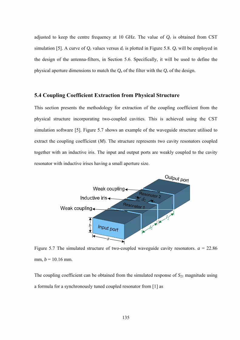
135
adjusted to keep the centre frequency at 10 GHz. The value of Qr is obtained from CST
simulation [5]. A curve of Qr values versus dr is plotted in Figure 5.8. Qr will be employed in
the design of the antenna-filters, in Section 5.6. Specifically, it will be used to define the
physical aperture dimensions to match the Qe of the filter with the Qr of the design.
5.4 Coupling Coefficient Extraction from Physical Structure
This section presents the methodology for extraction of the coupling coefficient from the
physical structure incorporating two-coupled cavities. This is achieved using the CST
simulation software [5]. Figure 5.7 shows an example of the waveguide structure utilised to
extract the coupling coefficient (M). The structure represents two cavity resonators coupled
together with an inductive iris. The input and output ports are weakly coupled to the cavity
resonator with inductive irises having a small aperture size.
Figure 5.7 The simulated structure of two-coupled waveguide cavity resonators. a = 22.86
mm, b = 10.16 mm.
The coupling coefficient can be obtained from the simulated response of S21 magnitude using
a formula for a synchronously tuned coupled resonator from [1] as
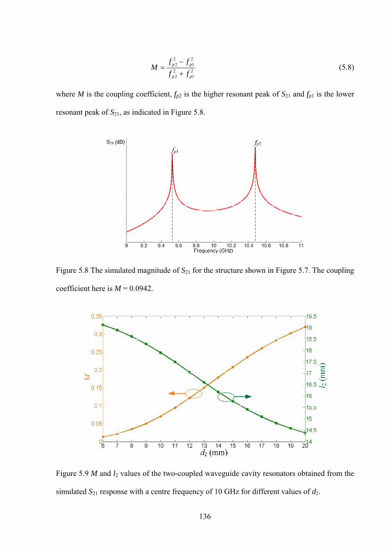
136
2 22 1
2 22 1
p p
p p
f fM
f f
(5.8)
where M is the coupling coefficient, fp2 is the higher resonant peak of S21 and fp1 is the lower
resonant peak of S21, as indicated in Figure 5.8.
Figure 5.8 The simulated magnitude of S21 for the structure shown in Figure 5.7. The coupling
coefficient here is M = 0.0942.
Figure 5.9 M and l2 values of the two-coupled waveguide cavity resonators obtained from the
simulated S21 response with a centre frequency of 10 GHz for different values of d2.

137
The simulated structure, shown in Figure 5.7, can be utilised to obtain the M values for
different values of d2 from the simulated S21 response using equation (5.8). Here l2 has been
adjusted to keep the centre frequency of 10 GHz. The M and l2 values for different values of
d2 are plotted in Figure 5.9. The graph showing M will be utilised in the design of antenna-
filter, in Section 5.6.
The self-coupling coefficient Mii is related to the self-resonant frequency of the
resonator i in a filter. For the case of asynchronous tuning, it is defined by [7]
2 20 02 2
0 0
2 iii
i
f fM
f f
(5.9)
where f0i is the resonant frequency of the resonator i and f0 is the desired centre frequency.
Equation (5.9) can be used to extracting the self-coupling coefficient Mii from the waveguide
structure for the design of an antenna-diplexer, in Section 5.8.
5.5 Coupling Matrix Synthesis for Multiple Port Antenna-Filters
In this work, the coupling matrix of the antenna-filter circuit is chosen for the design.
It is used in a similar way to the coupled-resonator two-port filter circuits [1] and Chapter 2.
Here the radiation inputs/outputs of proposed antenna-filters are considered as the
input/output ports of the equivalent filter. Matrix [A] can be expressed as [8]
[ ] [ ] [ ] [ ]A q p U j m (5.10)
where [U] is the n x n unit matrix, p is the complex frequency variable i.e. p = (j/FBW)(f/f0 –
f0/f), f0 is the centre frequency and FBW is the fractional bandwidth, [q] is an n x n matrix
with all entries zero, except for qii = 1/qei for the input/output ports and qii = 1/qri for the
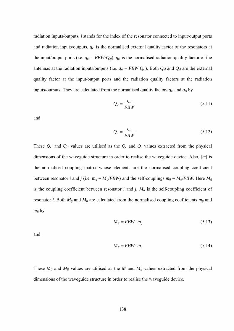
138
radiation inputs/outputs, i stands for the index of the resonator connected to input/output ports
and radiation inputs/outputs, qei is the normalised external quality factor of the resonators at
the input/output ports (i.e. qei = FBW·Qei), qri is the normalised radiation quality factor of the
antennas at the radiation inputs/outputs (i.e. qri = FBW·Qri). Both Qei and Qri are the external
quality factor at the input/output ports and the radiation quality factors at the radiation
inputs/outputs. They are calculated from the normalised quality factors qei and qri by
eiei
FBW (5.11)
and
riri
FBW (5.12)
These Qei and Qri values are utilised as the Qe and Qr values extracted from the physical
dimensions of the waveguide structure in order to realise the waveguide device. Also, [m] is
the normalised coupling matrix whose elements are the normalised coupling coefficient
between resonator i and j (i.e. mij = Mij/FBW) and the self-couplings mii = Mii/FBW. Here Mij
is the coupling coefficient between resonator i and j, Mii is the self-coupling coefficient of
resonator i. Both Mij and Mii are calculated from the normalised coupling coefficients mij and
mii by
ij ijM FBW m (5.13)
and
ii iiM FBW m (5.14)
These Mij and Mii values are utilised as the M and Mii values extracted from the physical
dimensions of the waveguide structure in order to realise the waveguide device.
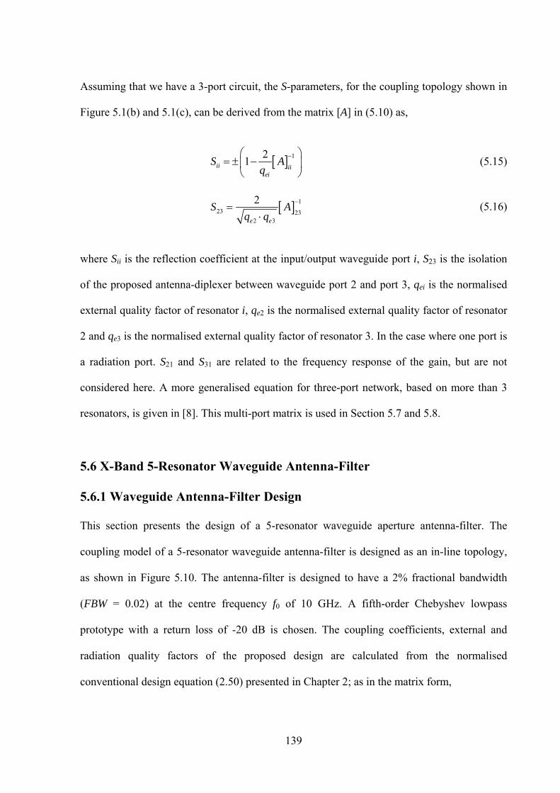
139
Assuming that we have a 3-port circuit, the S-parameters, for the coupling topology shown in
Figure 5.1(b) and 5.1(c), can be derived from the matrix [A] in (5.10) as,
121ii ii
ei
S Aq
(5.15)
1
23 232 3
2
e e
S Aq q
(5.16)
where Sii is the reflection coefficient at the input/output waveguide port i, S23 is the isolation
of the proposed antenna-diplexer between waveguide port 2 and port 3, qei is the normalised
external quality factor of resonator i, qe2 is the normalised external quality factor of resonator
2 and qe3 is the normalised external quality factor of resonator 3. In the case where one port is
a radiation port. S21 and S31 are related to the frequency response of the gain, but are not
considered here. A more generalised equation for three-port network, based on more than 3
resonators, is given in [8]. This multi-port matrix is used in Section 5.7 and 5.8.
5.6 X-Band 5-Resonator Waveguide Antenna-Filter
5.6.1 Waveguide Antenna-Filter Design
This section presents the design of a 5-resonator waveguide aperture antenna-filter. The
coupling model of a 5-resonator waveguide antenna-filter is designed as an in-line topology,
as shown in Figure 5.10. The antenna-filter is designed to have a 2% fractional bandwidth
(FBW = 0.02) at the centre frequency f0 of 10 GHz. A fifth-order Chebyshev lowpass
prototype with a return loss of -20 dB is chosen. The coupling coefficients, external and
radiation quality factors of the proposed design are calculated from the normalised
conventional design equation (2.50) presented in Chapter 2; as in the matrix form,

140
0 0.866 0 0 0
0.866 0 0.636 0 0
0 0.636 0 0.636 0
0 0 0.636 0 0.866
0 0 0 0.866 0
m
qe1 = qr5 = 0.9714
The calculated response of the S11 can be calculated from the values of [m], qe1 and qr5, using
equation (5.15), the result is shown in Figure 5.11.
Figure 5.10 Topology of the designed waveguide antenna-filter.
Figure 5.11 S11 in dB for the designed waveguide antenna-filter calculated from the coupling
matrix.
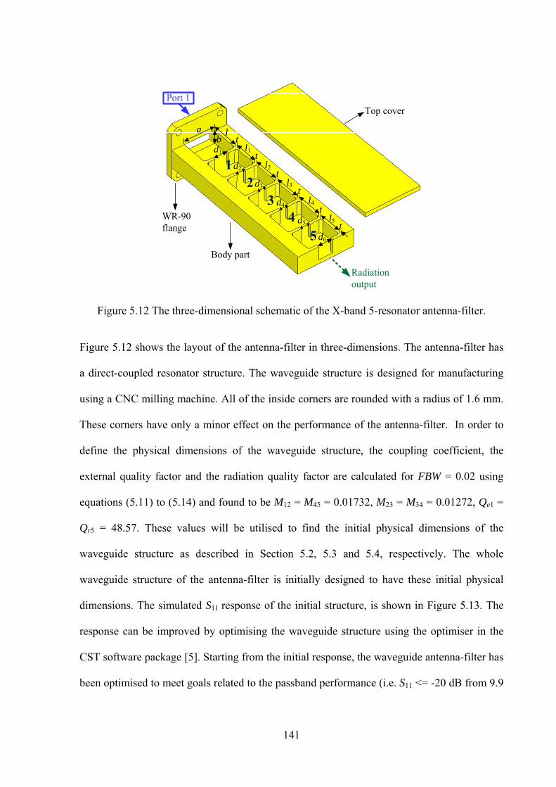
141
12
34
5
ab t
t
t
t
t
t
l
l1
l2
l3
l4
l5
d1
d2
d3
d4
d5
d6
Port 1
Radiation output
Top cover
WR-90 flange
Body part
Figure 5.12 The three-dimensional schematic of the X-band 5-resonator antenna-filter.
Figure 5.12 shows the layout of the antenna-filter in three-dimensions. The antenna-filter has
a direct-coupled resonator structure. The waveguide structure is designed for manufacturing
using a CNC milling machine. All of the inside corners are rounded with a radius of 1.6 mm.
These corners have only a minor effect on the performance of the antenna-filter. In order to
define the physical dimensions of the waveguide structure, the coupling coefficient, the
external quality factor and the radiation quality factor are calculated for FBW = 0.02 using
equations (5.11) to (5.14) and found to be M12 = M45 = 0.01732, M23 = M34 = 0.01272, Qe1 =
Qr5 = 48.57. These values will be utilised to find the initial physical dimensions of the
waveguide structure as described in Section 5.2, 5.3 and 5.4, respectively. The whole
waveguide structure of the antenna-filter is initially designed to have these initial physical
dimensions. The simulated S11 response of the initial structure, is shown in Figure 5.13. The
response can be improved by optimising the waveguide structure using the optimiser in the
CST software package [5]. Starting from the initial response, the waveguide antenna-filter has
been optimised to meet goals related to the passband performance (i.e. S11 <= -20 dB from 9.9
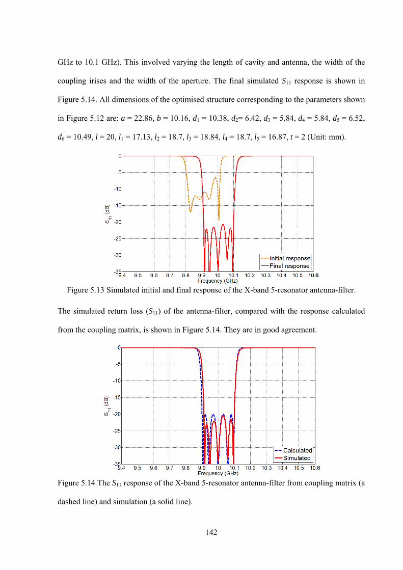
142
GHz to 10.1 GHz). This involved varying the length of cavity and antenna, the width of the
coupling irises and the width of the aperture. The final simulated S11 response is shown in
Figure 5.14. All dimensions of the optimised structure corresponding to the parameters shown
in Figure 5.12 are: a = 22.86, b = 10.16, d1 = 10.38, d2= 6.42, d3 = 5.84, d4 = 5.84, d5 = 6.52,
d6 = 10.49, l = 20, l1 = 17.13, l2 = 18.7, l3 = 18.84, l4 = 18.7, l5 = 16.87, t = 2 (Unit: mm).
Figure 5.13 Simulated initial and final response of the X-band 5-resonator antenna-filter.
The simulated return loss (S11) of the antenna-filter, compared with the response calculated
from the coupling matrix, is shown in Figure 5.14. They are in good agreement.
Figure 5.14 The S11 response of the X-band 5-resonator antenna-filter from coupling matrix (a
dashed line) and simulation (a solid line).
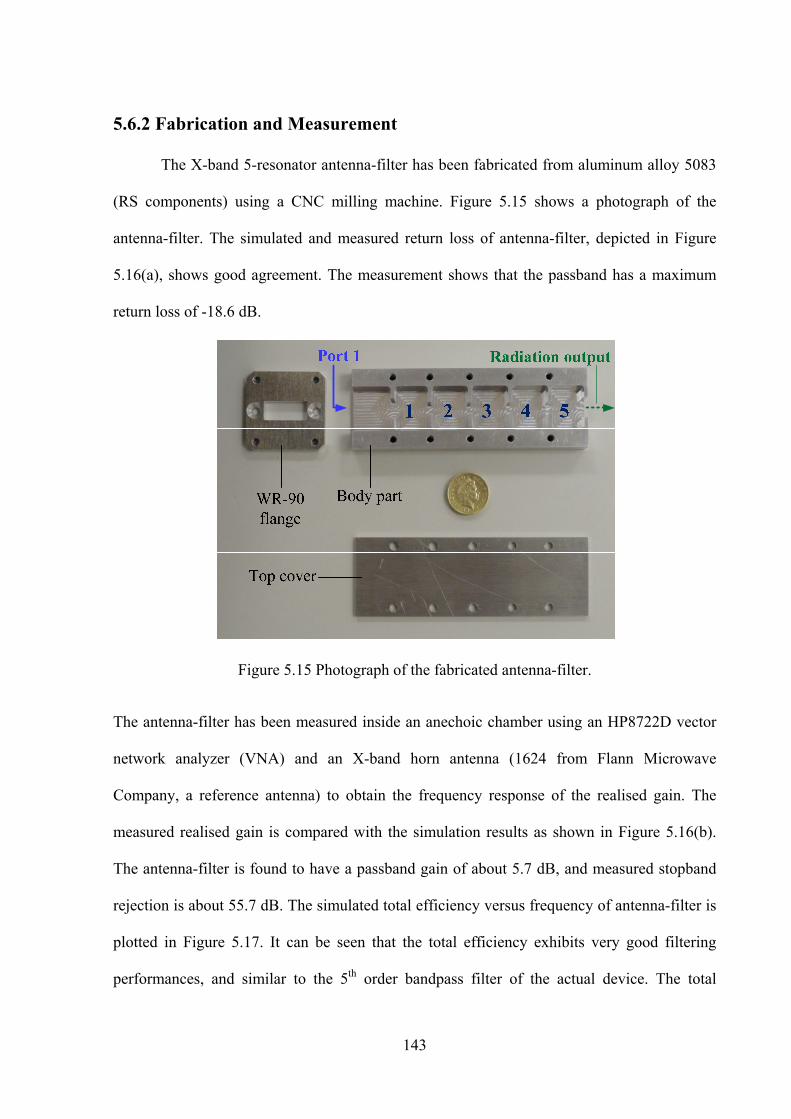
143
5.6.2 Fabrication and Measurement
The X-band 5-resonator antenna-filter has been fabricated from aluminum alloy 5083
(RS components) using a CNC milling machine. Figure 5.15 shows a photograph of the
antenna-filter. The simulated and measured return loss of antenna-filter, depicted in Figure
5.16(a), shows good agreement. The measurement shows that the passband has a maximum
return loss of -18.6 dB.
Figure 5.15 Photograph of the fabricated antenna-filter.
The antenna-filter has been measured inside an anechoic chamber using an HP8722D vector
network analyzer (VNA) and an X-band horn antenna (1624 from Flann Microwave
Company, a reference antenna) to obtain the frequency response of the realised gain. The
measured realised gain is compared with the simulation results as shown in Figure 5.16(b).
The antenna-filter is found to have a passband gain of about 5.7 dB, and measured stopband
rejection is about 55.7 dB. The simulated total efficiency versus frequency of antenna-filter is
plotted in Figure 5.17. It can be seen that the total efficiency exhibits very good filtering
performances, and similar to the 5th order bandpass filter of the actual device. The total
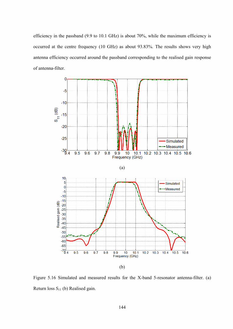
144
efficiency in the passband (9.9 to 10.1 GHz) is about 70%, while the maximum efficiency is
occurred at the centre frequency (10 GHz) as about 93.83%. The results shows very high
antenna efficiency occurred around the passband corresponding to the realised gain response
of antenna-filter.
(a)
(b)
Figure 5.16 Simulated and measured results for the X-band 5-resonator antenna-filter. (a)
Return loss S11 (b) Realised gain.
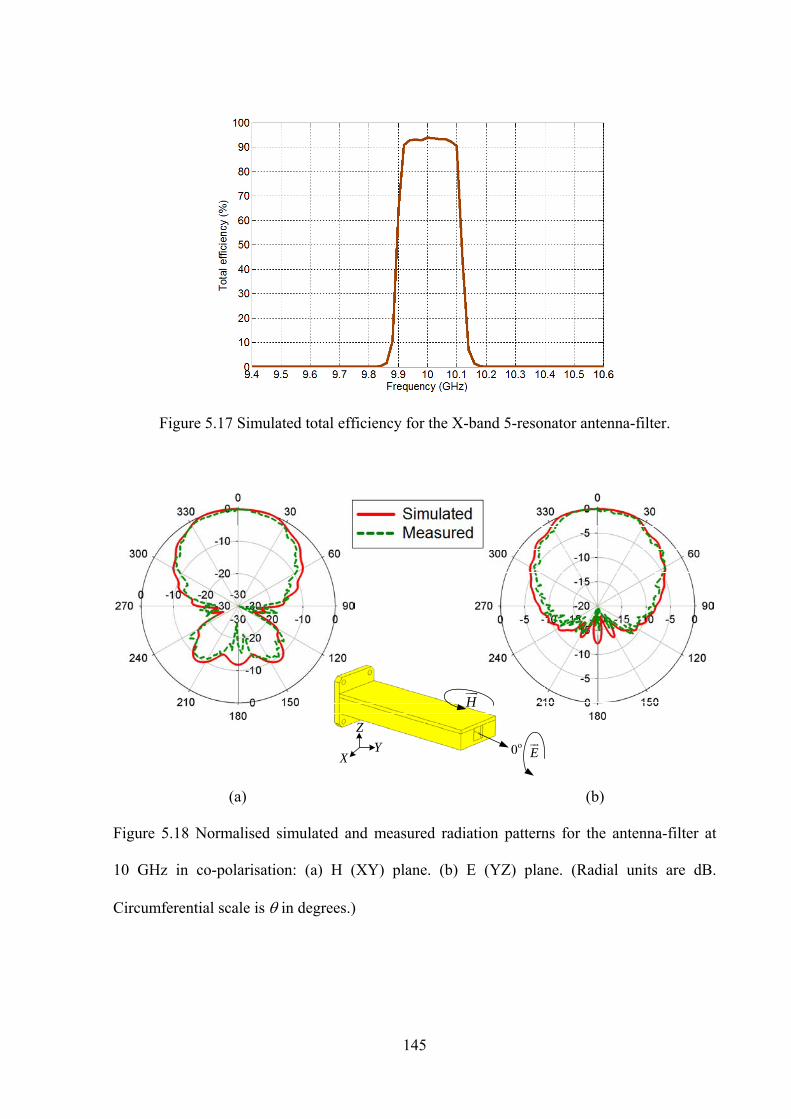
145
Figure 5.17 Simulated total efficiency for the X-band 5-resonator antenna-filter.
0o
H
E
Z
XY
(a) (b) Figure 5.18 Normalised simulated and measured radiation patterns for the antenna-filter at
10 GHz in co-polarisation: (a) H (XY) plane. (b) E (YZ) plane. (Radial units are dB.
Circumferential scale is in degrees.)
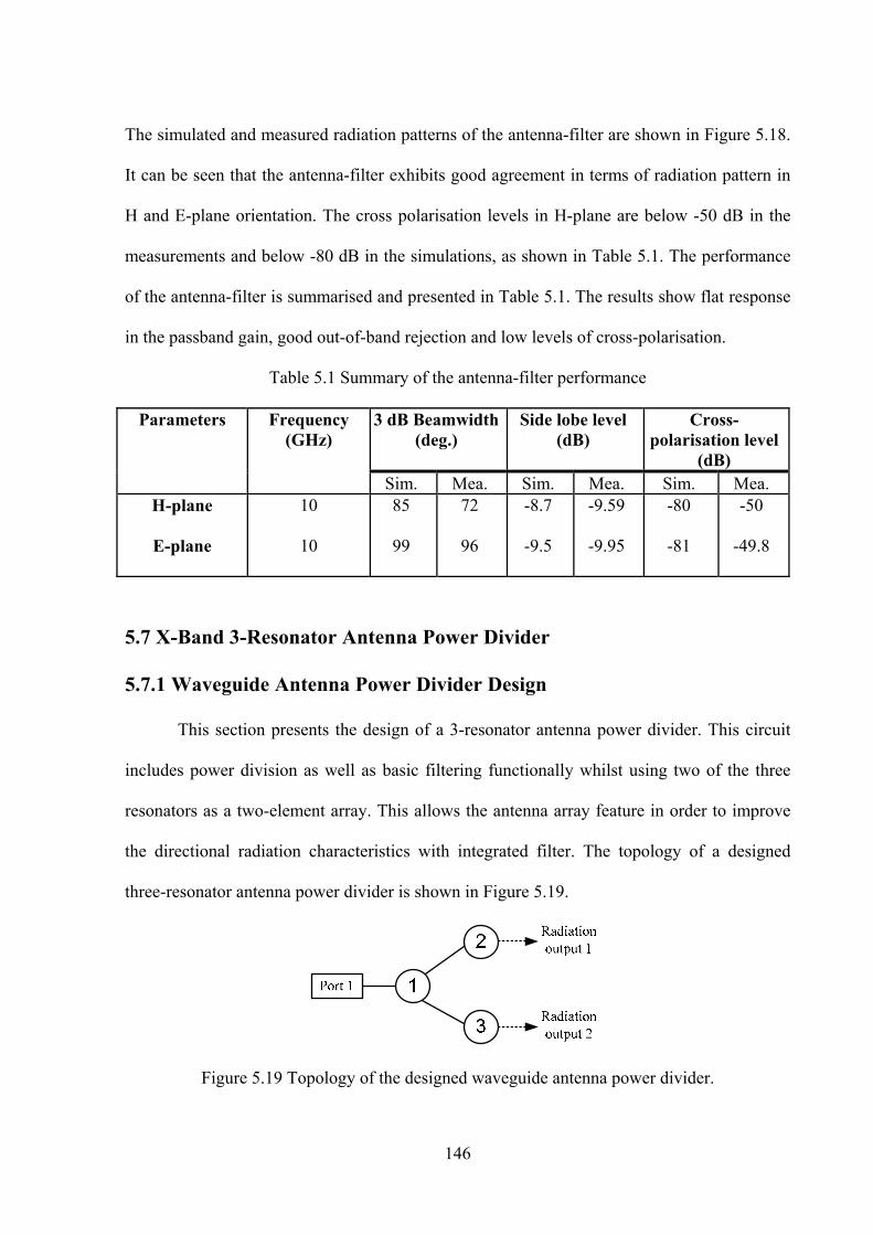
146
The simulated and measured radiation patterns of the antenna-filter are shown in Figure 5.18.
It can be seen that the antenna-filter exhibits good agreement in terms of radiation pattern in
H and E-plane orientation. The cross polarisation levels in H-plane are below -50 dB in the
measurements and below -80 dB in the simulations, as shown in Table 5.1. The performance
of the antenna-filter is summarised and presented in Table 5.1. The results show flat response
in the passband gain, good out-of-band rejection and low levels of cross-polarisation.
Table 5.1 Summary of the antenna-filter performance
Parameters Frequency (GHz)
3 dB Beamwidth (deg.)
Side lobe level (dB)
Cross-polarisation level
(dB) Sim. Mea. Sim. Mea. Sim. Mea.
H-plane
E-plane
10
10
85
99
72
96
-8.7
-9.5
-9.59
-9.95
-80
-81
-50
-49.8
5.7 X-Band 3-Resonator Antenna Power Divider
5.7.1 Waveguide Antenna Power Divider Design
This section presents the design of a 3-resonator antenna power divider. This circuit
includes power division as well as basic filtering functionally whilst using two of the three
resonators as a two-element array. This allows the antenna array feature in order to improve
the directional radiation characteristics with integrated filter. The topology of a designed
three-resonator antenna power divider is shown in Figure 5.19.
Figure 5.19 Topology of the designed waveguide antenna power divider.
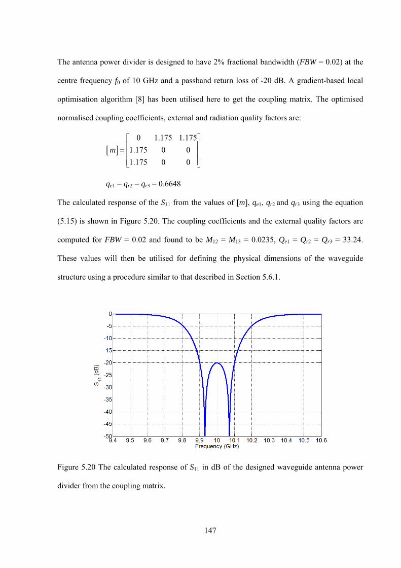
147
The antenna power divider is designed to have 2% fractional bandwidth (FBW = 0.02) at the
centre frequency f0 of 10 GHz and a passband return loss of -20 dB. A gradient-based local
optimisation algorithm [8] has been utilised here to get the coupling matrix. The optimised
normalised coupling coefficients, external and radiation quality factors are:
0 1.175 1.175
1.175 0 0
1.175 0 0
m
qe1 = qr2 = qr3 = 0.6648
The calculated response of the S11 from the values of [m], qe1, qr2 and qr3 using the equation
(5.15) is shown in Figure 5.20. The coupling coefficients and the external quality factors are
computed for FBW = 0.02 and found to be M12 = M13 = 0.0235, Qe1 = Qr2 = Qr3 = 33.24.
These values will then be utilised for defining the physical dimensions of the waveguide
structure using a procedure similar to that described in Section 5.6.1.
Figure 5.20 The calculated response of S11 in dB of the designed waveguide antenna power
divider from the coupling matrix.
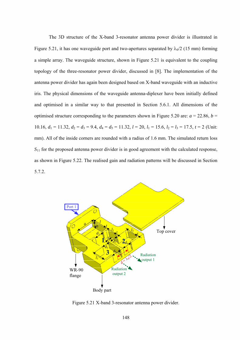
148
The 3D structure of the X-band 3-resonator antenna power divider is illustrated in
Figure 5.21, it has one waveguide port and two-apertures separated by 0/2 (15 mm) forming
a simple array. The waveguide structure, shown in Figure 5.21 is equivalent to the coupling
topology of the three-resonator power divider, discussed in [8]. The implementation of the
antenna power divider has again been designed based on X-band waveguide with an inductive
iris. The physical dimensions of the waveguide antenna-diplexer have been initially defined
and optimised in a similar way to that presented in Section 5.6.1. All dimensions of the
optimised structure corresponding to the parameters shown in Figure 5.20 are: a = 22.86, b =
10.16, d1 = 11.32, d2 = d3 = 9.4, d4 = d5 = 11.32, l = 20, l1 = 15.6, l2 = l3 = 17.5, t = 2 (Unit:
mm). All of the inside corners are rounded with a radius of 1.6 mm. The simulated return loss
S11 for the proposed antenna power divider is in good agreement with the calculated response,
as shown in Figure 5.22. The realised gain and radiation patterns will be discussed in Section
5.7.2.
d = 0/2
ab
l
l1d1
d2
d3
d4
d5
l2
l3
ttt
t
Radiation output 1
Radiation output 2
Port 1
3
Top cover
WR-90 flange
Body part
1 2
Figure 5.21 X-band 3-resonator antenna power divider.
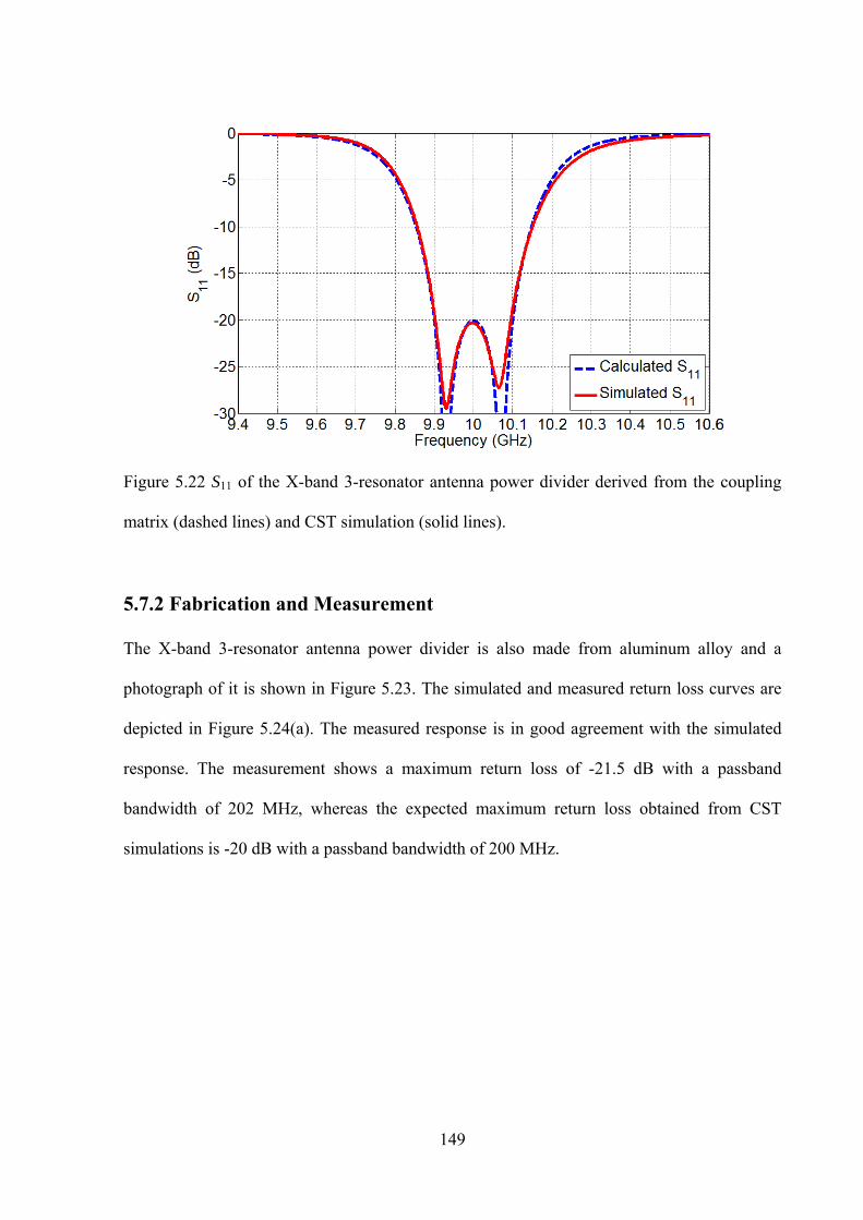
149
Figure 5.22 S11 of the X-band 3-resonator antenna power divider derived from the coupling
matrix (dashed lines) and CST simulation (solid lines).
5.7.2 Fabrication and Measurement
The X-band 3-resonator antenna power divider is also made from aluminum alloy and a
photograph of it is shown in Figure 5.23. The simulated and measured return loss curves are
depicted in Figure 5.24(a). The measured response is in good agreement with the simulated
response. The measurement shows a maximum return loss of -21.5 dB with a passband
bandwidth of 202 MHz, whereas the expected maximum return loss obtained from CST
simulations is -20 dB with a passband bandwidth of 200 MHz.
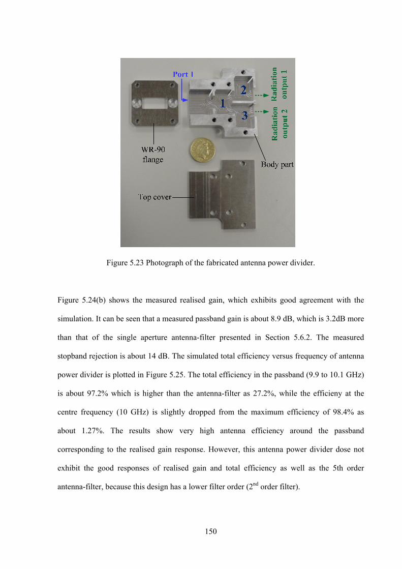
150
Figure 5.23 Photograph of the fabricated antenna power divider.
Figure 5.24(b) shows the measured realised gain, which exhibits good agreement with the
simulation. It can be seen that a measured passband gain is about 8.9 dB, which is 3.2dB more
than that of the single aperture antenna-filter presented in Section 5.6.2. The measured
stopband rejection is about 14 dB. The simulated total efficiency versus frequency of antenna
power divider is plotted in Figure 5.25. The total efficiency in the passband (9.9 to 10.1 GHz)
is about 97.2% which is higher than the antenna-filter as 27.2%, while the efficieny at the
centre frequency (10 GHz) is slightly dropped from the maximum efficiency of 98.4% as
about 1.27%. The results show very high antenna efficiency around the passband
corresponding to the realised gain response. However, this antenna power divider dose not
exhibit the good responses of realised gain and total efficiency as well as the 5th order
antenna-filter, because this design has a lower filter order (2nd order filter).
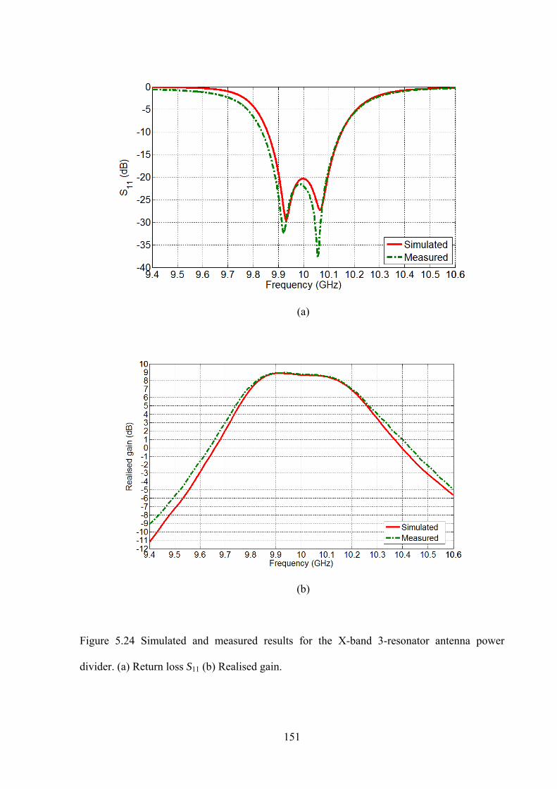
151
(a)
(b)
Figure 5.24 Simulated and measured results for the X-band 3-resonator antenna power
divider. (a) Return loss S11 (b) Realised gain.
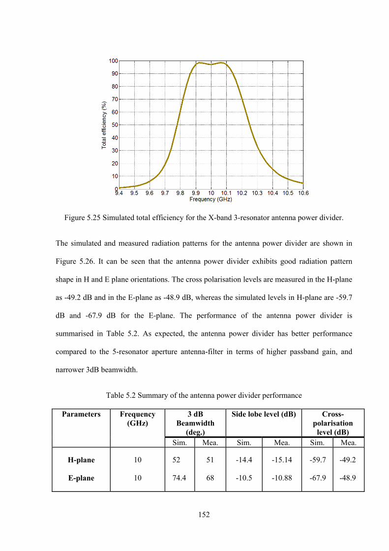
152
Figure 5.25 Simulated total efficiency for the X-band 3-resonator antenna power divider.
The simulated and measured radiation patterns for the antenna power divider are shown in
Figure 5.26. It can be seen that the antenna power divider exhibits good radiation pattern
shape in H and E plane orientations. The cross polarisation levels are measured in the H-plane
as -49.2 dB and in the E-plane as -48.9 dB, whereas the simulated levels in H-plane are -59.7
dB and -67.9 dB for the E-plane. The performance of the antenna power divider is
summarised in Table 5.2. As expected, the antenna power divider has better performance
compared to the 5-resonator aperture antenna-filter in terms of higher passband gain, and
narrower 3dB beamwidth.
Table 5.2 Summary of the antenna power divider performance
Parameters Frequency (GHz)
3 dB Beamwidth
(deg.)
Side lobe level (dB)
Cross-polarisation
level (dB) Sim. Mea. Sim. Mea. Sim. Mea.
H-plane
E-plane
10
10
52
74.4
51
68
-14.4
-10.5
-15.14
-10.88
-59.7
-67.9
-49.2
-48.9
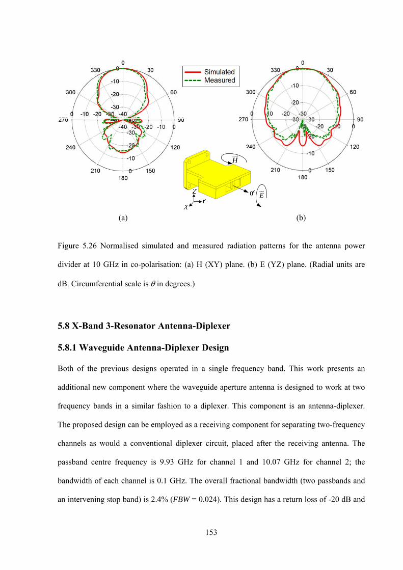
153
H
E
(a) (b)
Figure 5.26 Normalised simulated and measured radiation patterns for the antenna power
divider at 10 GHz in co-polarisation: (a) H (XY) plane. (b) E (YZ) plane. (Radial units are
dB. Circumferential scale is in degrees.)
5.8 X-Band 3-Resonator Antenna-Diplexer
5.8.1 Waveguide Antenna-Diplexer Design
Both of the previous designs operated in a single frequency band. This work presents an
additional new component where the waveguide aperture antenna is designed to work at two
frequency bands in a similar fashion to a diplexer. This component is an antenna-diplexer.
The proposed design can be employed as a receiving component for separating two-frequency
channels as would a conventional diplexer circuit, placed after the receiving antenna. The
passband centre frequency is 9.93 GHz for channel 1 and 10.07 GHz for channel 2; the
bandwidth of each channel is 0.1 GHz. The overall fractional bandwidth (two passbands and
an intervening stop band) is 2.4% (FBW = 0.024). This design has a return loss of -20 dB and
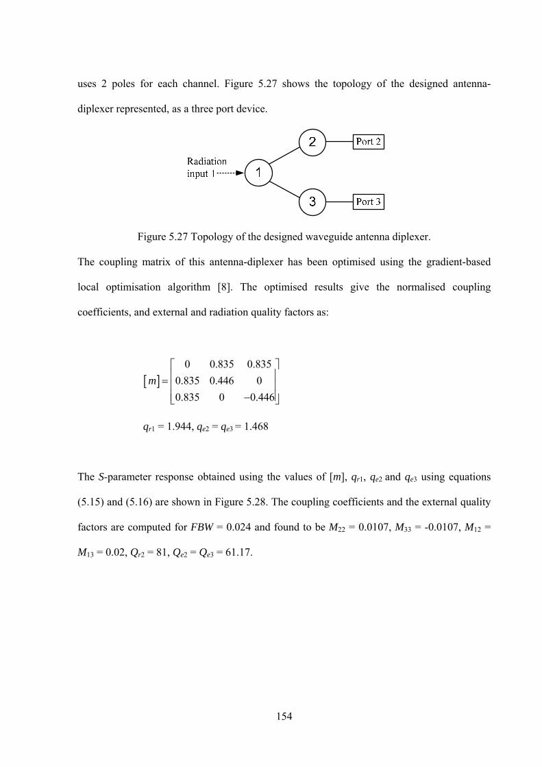
154
uses 2 poles for each channel. Figure 5.27 shows the topology of the designed antenna-
diplexer represented, as a three port device.
Figure 5.27 Topology of the designed waveguide antenna diplexer.
The coupling matrix of this antenna-diplexer has been optimised using the gradient-based
local optimisation algorithm [8]. The optimised results give the normalised coupling
coefficients, and external and radiation quality factors as:
0 0.835 0.835
0.835 0.446 0
0.835 0 0.446
m
qr1 = 1.944, qe2 = qe3 = 1.468
The S-parameter response obtained using the values of [m], qr1, qe2 and qe3 using equations
(5.15) and (5.16) are shown in Figure 5.28. The coupling coefficients and the external quality
factors are computed for FBW = 0.024 and found to be M22 = 0.0107, M33 = -0.0107, M12 =
M13 = 0.02, Qr2 = 81, Qe2 = Qe3 = 61.17.
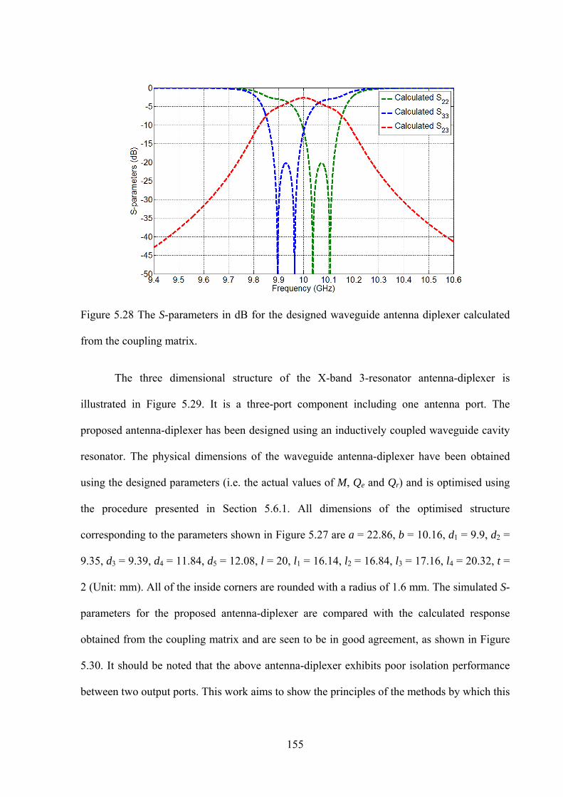
155
Figure 5.28 The S-parameters in dB for the designed waveguide antenna diplexer calculated
from the coupling matrix.
The three dimensional structure of the X-band 3-resonator antenna-diplexer is
illustrated in Figure 5.29. It is a three-port component including one antenna port. The
proposed antenna-diplexer has been designed using an inductively coupled waveguide cavity
resonator. The physical dimensions of the waveguide antenna-diplexer have been obtained
using the designed parameters (i.e. the actual values of M, Qe and Qr) and is optimised using
the procedure presented in Section 5.6.1. All dimensions of the optimised structure
corresponding to the parameters shown in Figure 5.27 are a = 22.86, b = 10.16, d1 = 9.9, d2 =
9.35, d3 = 9.39, d4 = 11.84, d5 = 12.08, l = 20, l1 = 16.14, l2 = 16.84, l3 = 17.16, l4 = 20.32, t =
2 (Unit: mm). All of the inside corners are rounded with a radius of 1.6 mm. The simulated S-
parameters for the proposed antenna-diplexer are compared with the calculated response
obtained from the coupling matrix and are seen to be in good agreement, as shown in Figure
5.30. It should be noted that the above antenna-diplexer exhibits poor isolation performance
between two output ports. This work aims to show the principles of the methods by which this
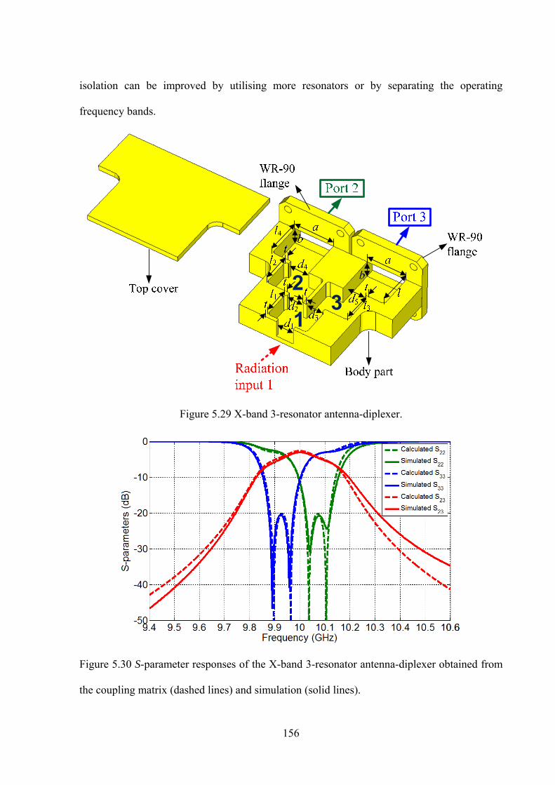
156
isolation can be improved by utilising more resonators or by separating the operating
frequency bands.
Figure 5.29 X-band 3-resonator antenna-diplexer.
Figure 5.30 S-parameter responses of the X-band 3-resonator antenna-diplexer obtained from
the coupling matrix (dashed lines) and simulation (solid lines).
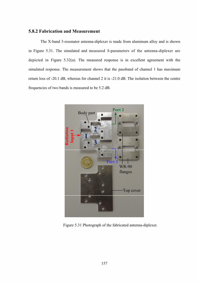
157
5.8.2 Fabrication and Measurement
The X-band 3-resonator antenna-diplexer is made from aluminum alloy and is shown
in Figure 5.31. The simulated and measured S-parameters of the antenna-diplexer are
depicted in Figure 5.32(a). The measured response is in excellent agreement with the
simulated response. The measurement shows that the passband of channel 1 has maximum
return loss of -20.1 dB, whereas for channel 2 it is -21.0 dB. The isolation between the centre
frequencies of two bands is measured to be 5.2 dB.
Port 2
WR-90 flanges
Body part
Top cover
Rad
iati
on
Inp
ut
1
Port 3
Figure 5.31 Photograph of the fabricated antenna-diplexer.
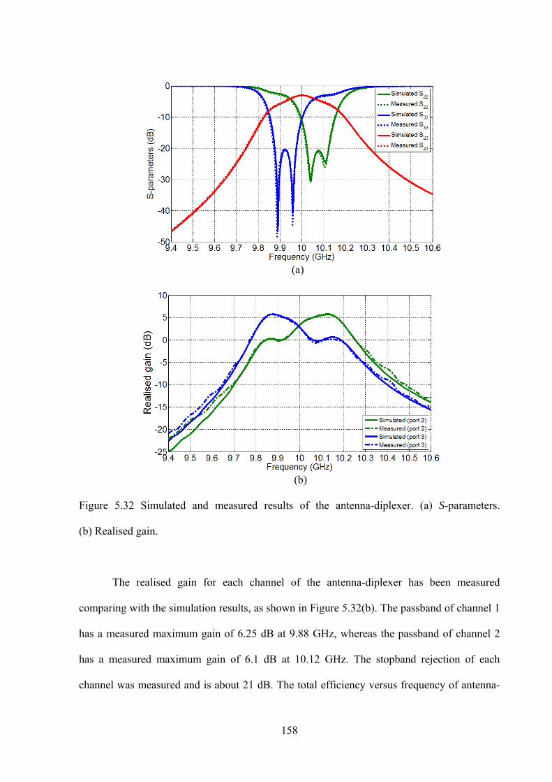
158
(a)
(b)
Figure 5.32 Simulated and measured results of the antenna-diplexer. (a) S-parameters.
(b) Realised gain.
The realised gain for each channel of the antenna-diplexer has been measured
comparing with the simulation results, as shown in Figure 5.32(b). The passband of channel 1
has a measured maximum gain of 6.25 dB at 9.88 GHz, whereas the passband of channel 2
has a measured maximum gain of 6.1 dB at 10.12 GHz. The stopband rejection of each
channel was measured and is about 21 dB. The total efficiency versus frequency of antenna-

159
diplexer is plotted with the simulation results, as shown in Figure 5.33. The passband of
channel 1 has a maximum total efficiency of 74.3% at 9.88 GHz, whereas the passband of
channel 2 has a maximum total efficiency of 71.38% dB at 10.12 GHz. The results show the
corresponding maximum realised gains with the maximum total efficiency at the same
frequency of each channel. However, the total efficiency and realised gain of antenna-diplexer
does not achieve better than previous designs. It can be achievable the good performance
since the number of antenna is increased with the antenna array design technique.
It should be noted that the results of Figure 5.32(a) show that on port 2, 20% of
received energy at the centre frequency goes to port 3 and vice versa. This work aims to show
the principle of the design method and this leaking of received energy between two output
ports can be improved by utilising more resonators and/or separating the bands.
Figure 5.33 Simulated total efficiency for the X-band 3-resonator antenna-diplexer.
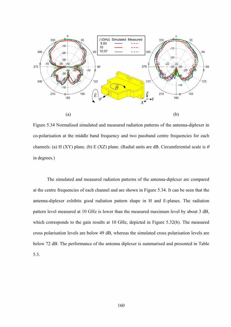
160
f (GHz) Simulated Measured9.931010.07
0o
H
E Z
XY
(a) (b) Figure 5.34 Normalised simulated and measured radiation patterns of the antenna-diplexer in
co-polarisation at the middle band frequency and two passband centre frequencies for each
channels: (a) H (XY) plane. (b) E (XZ) plane. (Radial units are dB. Circumferential scale is
in degrees.)
The simulated and measured radiation patterns of the antenna-diplexer are compared
at the centre frequencies of each channel and are shown in Figure 5.34. It can be seen that the
antenna-diplexer exhibits good radiation pattern shape in H and E-planes. The radiation
pattern level measured at 10 GHz is lower than the measured maximum level by about 3 dB,
which corresponds to the gain results at 10 GHz, depicted in Figure 5.32(b). The measured
cross polarisation levels are below 49 dB, whereas the simulated cross polarisation levels are
below 72 dB. The performance of the antenna diplexer is summarised and presented in Table
5.3.
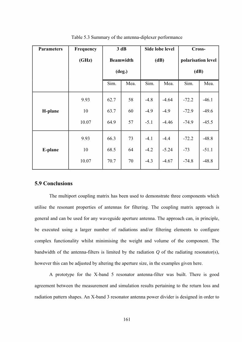
161
Table 5.3 Summary of the antenna-diplexer performance
Parameters Frequency
(GHz)
3 dB
Beamwidth
(deg.)
Side lobe level
(dB)
Cross-
polarisation level
(dB)
Sim. Mea. Sim. Mea. Sim. Mea.
H-plane
9.93
10
10.07
62.7
63.7
64.9
58
60
57
-4.8
-4.9
-5.1
-4.64
-4.9
-4.46
-72.2
-72.9
-74.9
-46.1
-49.6
-45.5
E-plane
9.93
10
10.07
66.3
68.5
70.7
73
64
70
-4.1
-4.2
-4.3
-4.4
-5.24
-4.67
-72.2
-73
-74.8
-48.8
-51.1
-48.8
5.9 Conclusions
The multiport coupling matrix has been used to demonstrate three components which
utilise the resonant properties of antennas for filtering. The coupling matrix approach is
general and can be used for any waveguide aperture antenna. The approach can, in principle,
be executed using a larger number of radiations and/or filtering elements to configure
complex functionality whilst minimising the weight and volume of the component. The
bandwidth of the antenna-filters is limited by the radiation Q of the radiating resonator(s),
however this can be adjusted by altering the aperture size, in the examples given here.
A prototype for the X-band 5 resonator antenna-filter was built. There is good
agreement between the measurement and simulation results pertaining to the return loss and
radiation pattern shapes. An X-band 3 resonator antenna power divider is designed in order to
162
improve antenna gain with compact size and is suitable for use in a transmitter. An X-band 3
resonator antenna-diplexer is designed for use in a receiver where it could be utilised as a
frequency splitter with compact size. The measurement results for this and the antenna-
diplexer agree very well with simulations. These proposed components have compact sizes,
light weights and small number of front-end microwave components, and as such they are
suitable for use of modern communication systems
References
[1] Hong J. S. and Lancaster M. J. Microstrip Filters for RF/Microwave Applications. New
York, USA: John Wiley & Sons; 2001.
[2] Pozar D. M. Microwave Engineering. 3rd ed. USA: John Wiley & Sons; 2005.
[3] Lancaster M. J. Passive Microwave Device Applications of High-Temperature
Superconductors. Cambridge, UK: Cambridge University Press; 1997.
[4] Collin R. E. Foundation for Microwave Engineering. 2nd ed. USA: John Wiley & Sons;
2011.
[5] Computer Simulation Technology (CST), Microwave Studio [Internet]. 2014 Available
from URL: http://www.cst.com.
[6] Matthaei G. L., Young L., Jones E.M.T. Microwave Filters, Impedance-matching
Networks and Coupling Structures. North Bergen, NJ, USA: Artech House, 1980.
[7] Talal F. Skaik, Synthesis of Coupled Resonator Circuits with Multiple Outputs using
Coupling Matrix Optimization, PhD thesis, University of Birmingham, UK, 2011.
[8] Skaik T., Lancaster M. J., and Huang F. Synthesis of multiple output coupled resonator
microwave circuits using coupling matrix optimization. IET J. Microw., Antennas,
Propag. 2011 Jun.; 5(9): 1081–1088.
163
Chapter 6
Conclusions and Future Work
6.1 Conclusions
This thesis presented new design techniques for antenna-filters involving use of
coupling matrix synthesis. The approach is applied to dipole and waveguide structures. The
work has been divided into three main parts: two port dipole antenna-filter, one port dipole
antenna-filter and waveguide antenna-filter.
The objective of the work presented in Chapter 3 was to design a coupled resonator
filter using antennas in order to help understand the antenna. In this work the antenna is
treated as a resonator within a filter circuit. A dipole antenna is selected as the resonator type
in this work. The structure of this antenna is simple and suited for designing the resonator.
The antennas can be arrayed to form an in-line structure which is suitable for design the two-
port coupled-resonator filter. The coupling matrix has been utilised to obtain the filter
response of the two-port dipole antenna-filter from specifications resulting in the design
parameters (quality factors and coupling coefficient). However, any loss in the filter needs to
be considered which consist of radiation, material and inductor loss. These losses are
associated with the low Qu value of the resonators which causes. The insertion loss of the
two-port dipole antenna-filter is 3.1 dB in simulation and is 3.4 dB in measurement, which are
in good agreement with the calculation obtained using the method in [1] which is about 3.5
dB. The proposed antenna-filter in Chapter 3 is a two-port device and has similar in structure
which is a conventional dipole antenna array. The design method used for two-port filter in
Chapter 3 can be utilised to design a one-port dipole antenna-filter presented in Chapter 4.
164
The work presented in Chapter 4 aimed to integrate the dipole antenna into a filter
circuit replacing the second port with a radiation port. All resonators in this antenna-filter are
dipole antennas integrated with inductors and can also be radiating elements. The work in
Chapter 4 has started looking at a 1st order antenna-filter for a clear understanding of the
concept of antenna and filter integration. The design of the 1st order dipole antenna-filter used
the coupling matrix synthesis to optimise the filter response with the optimised design
parameters (Qe1 and Qu1). The 1st order antenna-filter adjusts the Qe1 and Qu1 values by
changing the position between a feed and a resonator antenna. The realised gain response of
the 1st order antenna-filter has showed the similar shape of 1st order bandpass filter. The poor
realised gain for this design can be improved when the number of antenna elements is
increased as presented in 2nd and 3rd order designs. The 2nd order antenna-filter design is based
on the design concept of the antenna-filter work in the filter literature by assuming the Qu
value of the last resonator is the same Qe value of the input resonator to preserve the filter
characteristic. The design can be achieved with the optimised Qe value for this design as
described in Section 4.2.1. The measurement and simulation results showed in good
agreement. The realised gain of the 3rd order antenna-filter showed the filtering response with
good agreement between simulation and measurement. The work in Chapter4 has been
achieved following the principle theory of antenna and filter and the coupling matrix synthesis
for the antenna-filter component. This design method can be applicable in the coupled
resonator antenna-filter for different topologies, one of which is presented in Chapter 5.
The third part in Chapter 5 presented three design approaches of antenna-filters using
a waveguide structure [2]. All approaches have utilised waveguide aperture antennas as
resonators. A 5-resonator antenna-filter is the first design of this work and has an in-line
coupling topology with one input electrical port and one output is the radiation. The designed
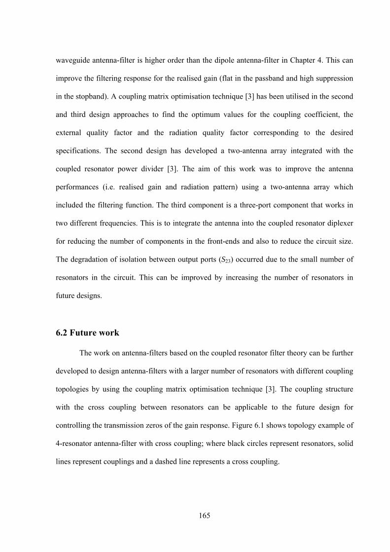
165
waveguide antenna-filter is higher order than the dipole antenna-filter in Chapter 4. This can
improve the filtering response for the realised gain (flat in the passband and high suppression
in the stopband). A coupling matrix optimisation technique [3] has been utilised in the second
and third design approaches to find the optimum values for the coupling coefficient, the
external quality factor and the radiation quality factor corresponding to the desired
specifications. The second design has developed a two-antenna array integrated with the
coupled resonator power divider [3]. The aim of this work was to improve the antenna
performances (i.e. realised gain and radiation pattern) using a two-antenna array which
included the filtering function. The third component is a three-port component that works in
two different frequencies. This is to integrate the antenna into the coupled resonator diplexer
for reducing the number of components in the front-ends and also to reduce the circuit size.
The degradation of isolation between output ports (S23) occurred due to the small number of
resonators in the circuit. This can be improved by increasing the number of resonators in
future designs.
6.2 Future work
The work on antenna-filters based on the coupled resonator filter theory can be further
developed to design antenna-filters with a larger number of resonators with different coupling
topologies by using the coupling matrix optimisation technique [3]. The coupling structure
with the cross coupling between resonators can be applicable to the future design for
controlling the transmission zeros of the gain response. Figure 6.1 shows topology example of
4-resonator antenna-filter with cross coupling; where black circles represent resonators, solid
lines represent couplings and a dashed line represents a cross coupling.
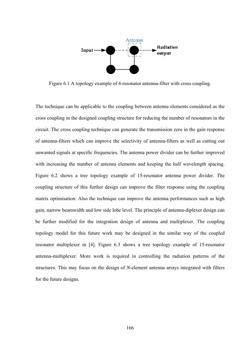
166
Figure 6.1 A topology example of 4-resonator antenna-filter with cross coupling.
The technique can be applicable to the coupling between antenna elements considered as the
cross coupling in the designed coupling structure for reducing the number of resonators in the
circuit. The cross coupling technique can generate the transmission zero in the gain response
of antenna-filters which can improve the selectivity of antenna-filters as well as cutting out
unwanted signals at specific frequencies. The antenna power divider can be further improved
with increasing the number of antenna elements and keeping the half wavelength spacing.
Figure 6.2 shows a tree topology example of 15-resonator antenna power divider. The
coupling structure of this further design can improve the filter response using the coupling
matrix optimisation. Also the technique can improve the antenna performances such as high
gain, narrow beamwidth and low side lobe level. The principle of antenna-diplexer design can
be further modified for the integration design of antenna and multiplexer. The coupling
topology model for this future work may be designed in the similar way of the coupled
resonator multiplexer in [4]. Figure 6.3 shows a tree topology example of 15-resonator
antenna-multiplexer. More work is required in controlling the radiation patterns of the
structures. This may focus on the design of N-element antenna arrays integrated with filters
for the future designs.
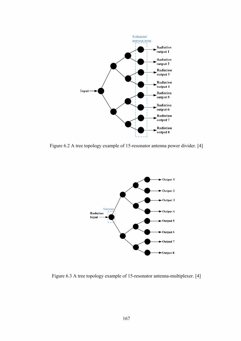
167
Figure 6.2 A tree topology example of 15-resonator antenna power divider. [4]
Figure 6.3 A tree topology example of 15-resonator antenna-multiplexer. [4]
168
References
[1] Hong J. S. and Lancaster M. J. Microstrip Filters for RF/Microwave Applications. New
York, USA: John Wiley & Sons; 2001.
[2] Pozar D. M. Microwave Engineering. 3rd ed. USA: John Wiley & Sons; 2005.
[3] Skaik T., Lancaster M. J., and Huang F. Synthesis of multiple output coupled resonator
microwave circuits using coupling matrix optimization. IET J. Microw., Antennas,
Propag. 2011 Jun.; 5(9): 1081–1088.
[4] Shang X., Wang Y., Xia W., Lancaster M. J. Novel Multiplexer Topologies Based on
All-Resonator Structures. IEEE Trans. Microw. Theory Tech. 2013 Nov.; 61(11): 3838–
3845.
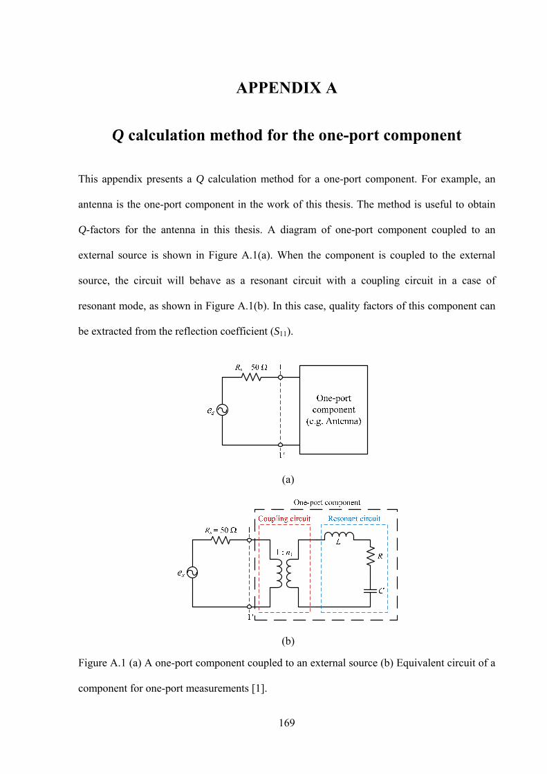
169
APPENDIX A
Q calculation method for the one-port component
This appendix presents a Q calculation method for a one-port component. For example, an
antenna is the one-port component in the work of this thesis. The method is useful to obtain
Q-factors for the antenna in this thesis. A diagram of one-port component coupled to an
external source is shown in Figure A.1(a). When the component is coupled to the external
source, the circuit will behave as a resonant circuit with a coupling circuit in a case of
resonant mode, as shown in Figure A.1(b). In this case, quality factors of this component can
be extracted from the reflection coefficient (S11).
(a)
(b)
Figure A.1 (a) A one-port component coupled to an external source (b) Equivalent circuit of a
component for one-port measurements [1].
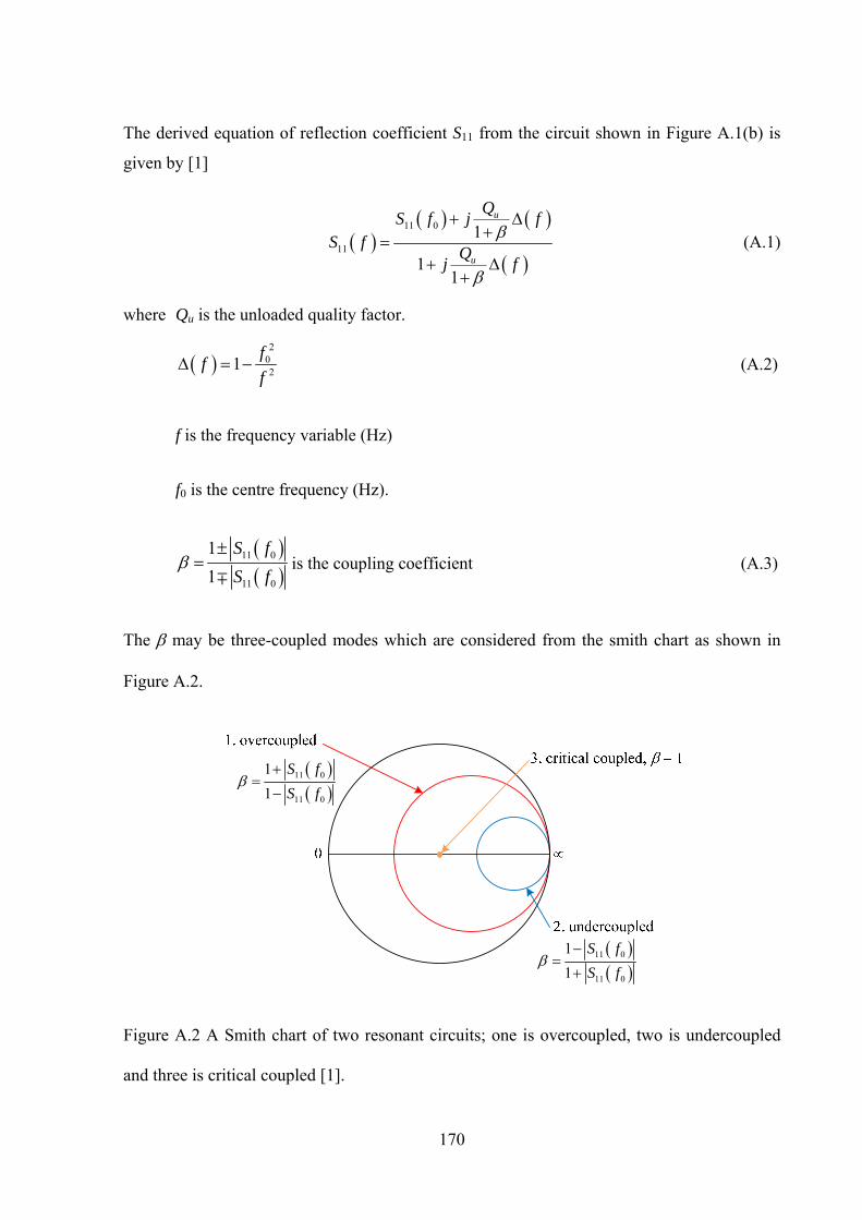
170
The derived equation of reflection coefficient S11 from the circuit shown in Figure A.1(b) is
given by [1]
11 0
11
1
11
u
u
QS f j f
S fQ
j f
(A.1)
where Qu is the unloaded quality factor.
2
02
1f
ff
(A.2)
f is the frequency variable (Hz)
f0 is the centre frequency (Hz).
11 0
11 0
1
1
S f
S f
is the coupling coefficient (A.3)
The may be three-coupled modes which are considered from the smith chart as shown in
Figure A.2.
11 0
11 0
1
1
S f
S f
11 0
11 0
1
1
S f
S f
Figure A.2 A Smith chart of two resonant circuits; one is overcoupled, two is undercoupled
and three is critical coupled [1].
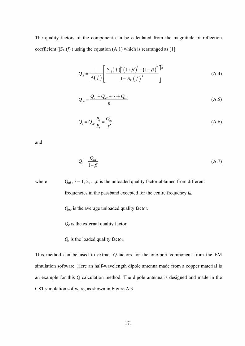
171
The quality factors of the component can be calculated from the magnitude of reflection
coefficient (|S11(f)|) using the equation (A.1) which is rearranged as [1]
12 2 2 2
11
2
11
1 11
1ui
S fQ
f S f
(A.4)
1 2u u unua
Q Q QQ
n
(A.5)
0 uae ua
e
P QQ Q
P (A.6)
and
1ua
l
(A.7)
where Qui , i = 1, 2, ...,n is the unloaded quality factor obtained from different
frequencies in the passband excepted for the centre frequency f0.
Qua is the average unloaded quality factor.
Qe is the external quality factor.
Ql is the loaded quality factor.
This method can be used to extract Q-factors for the one-port component from the EM
simulation software. Here an half-wavelength dipole antenna made from a copper material is
an example for this Q calculation method. The dipole antenna is designed and made in the
CST simulation software, as shown in Figure A.3.
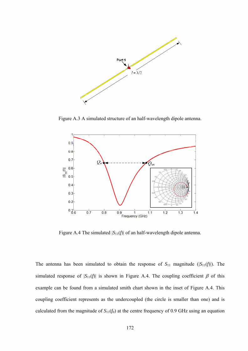
172
Figure A.3 A simulated structure of an half-wavelength dipole antenna.
Figure A.4 The simulated |S11(f)| of an half-wavelength dipole antenna.
The antenna has been simulated to obtain the response of S11 magnitude (|S11(f)|). The
simulated response of |S11(f)| is shown in Figure A.4. The coupling coefficient of this
example can be found from a simulated smith chart shown in the inset of Figure A.4. This
coupling coefficient represents as the undercoupled (the circle is smaller than one) and is
calculated from the magnitude of S11(f0) at the centre frequency of 0.9 GHz using an equation

173
(A.3). The calculated value using the equation (A.3) is 0.725. The Q-factors are calculated
from different values of |S11(f)| around half magnitude (0.15-0.65) of |S11(f)| within the
passband frequency (0.8 GHz–1.1 GHz) using equations (A.4) to (A.7). The calculated results
of average Q-factors are Qua = 5.26, Qe = 7.25 and Ql = 3.04. This is shown a calculation
example of the method and will be utilised in the work of this thesis. The method can be used
to obtain the radiation quality factor (Qr) for different antenna structure when the antenna is
made from a perfect electric conductor (PEC) material which considers the total Qu = Qr. This
has been described in Chapter 5.
References
[1] Lancaster M. J. Passive Microwave Device Applications of High-Temperature
Superconductors. Cambridge, UK: Cambridge University Press; 1997.

174
APPENDIX B
Publications
Nugoolcharoenlap E., Shang X., Lancaster M. and Huang F., “Design of Waveguide Aperture
Antenna-Filters using Coupling Matrix Theory” Submitted to Transaction on Microwave
Theory and Techniques on 5th Dec. 2014.
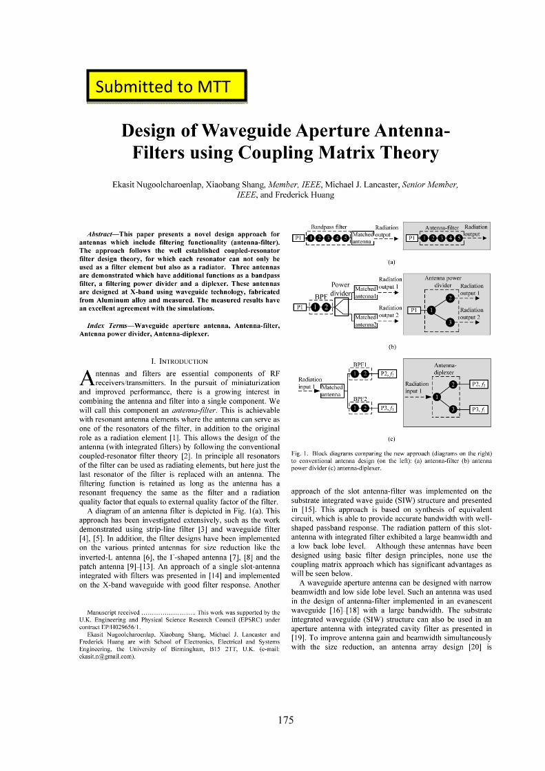
175
Submitted to MTT

176
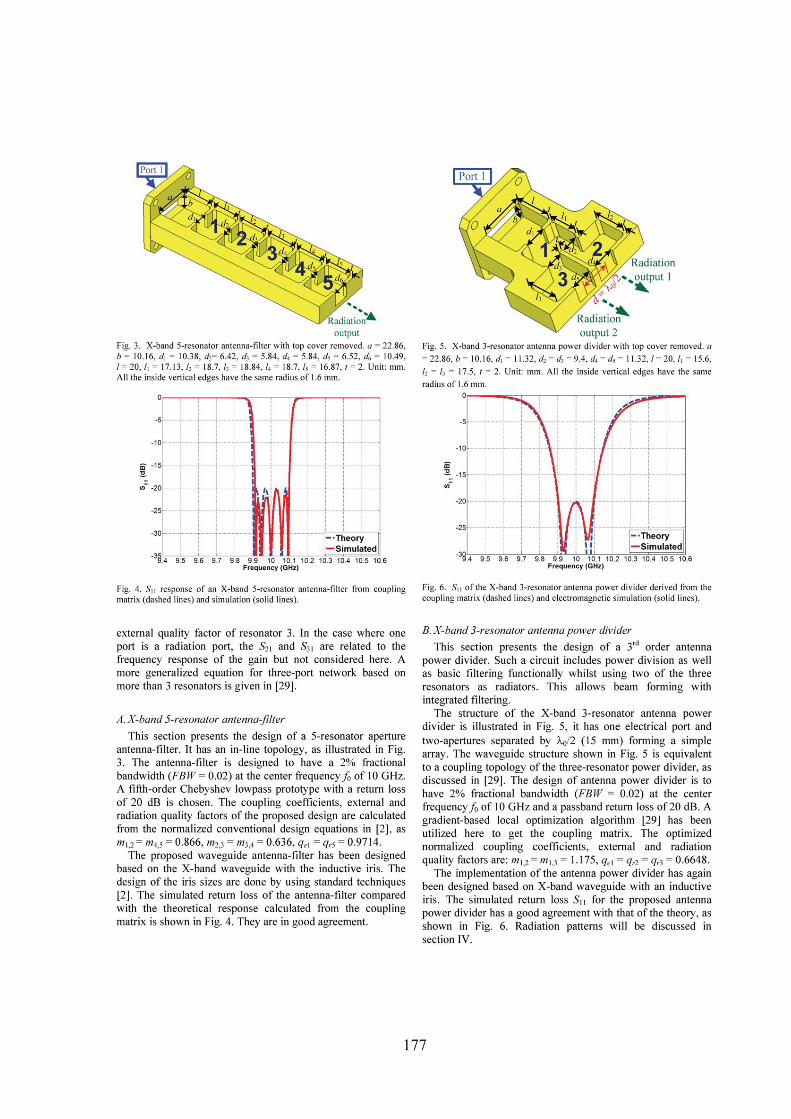
177
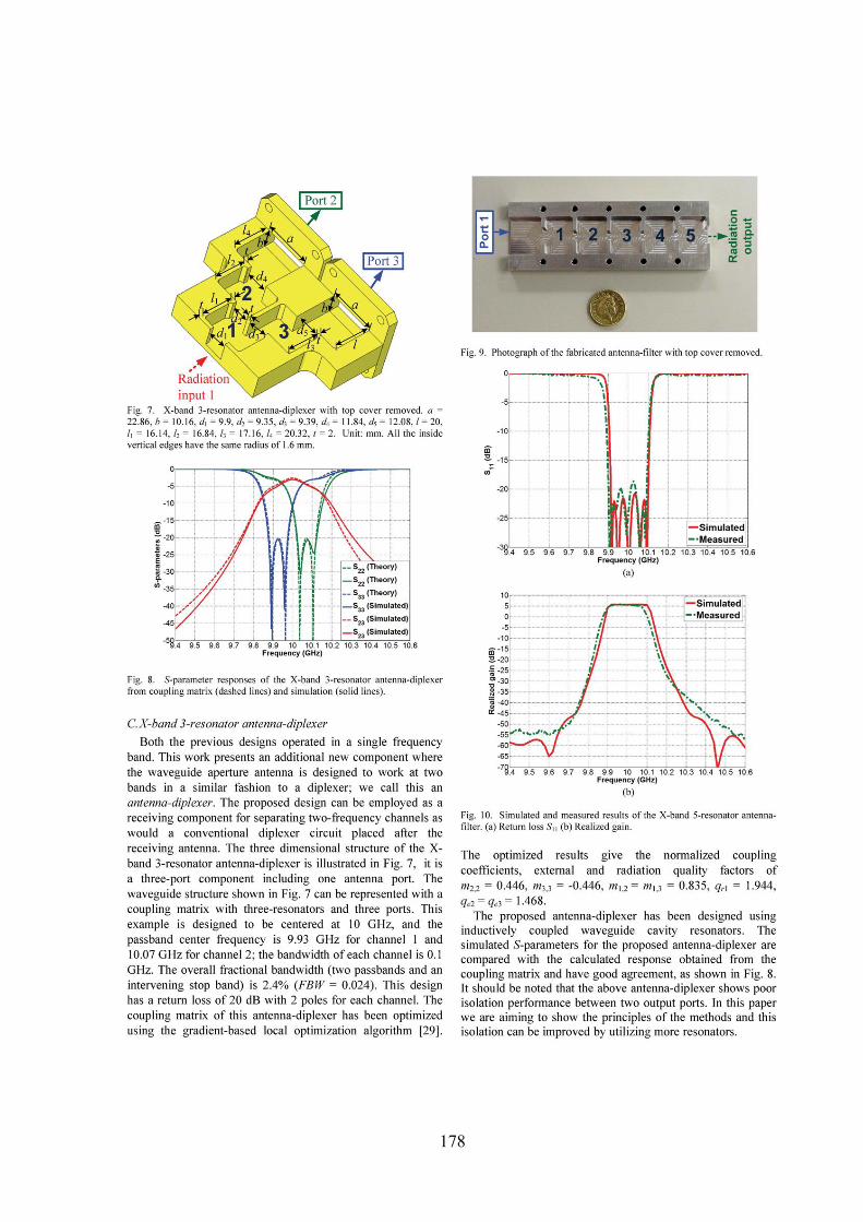
178
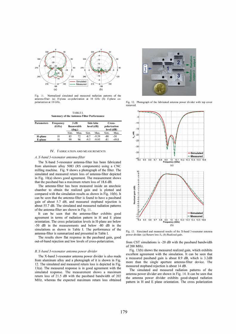
179
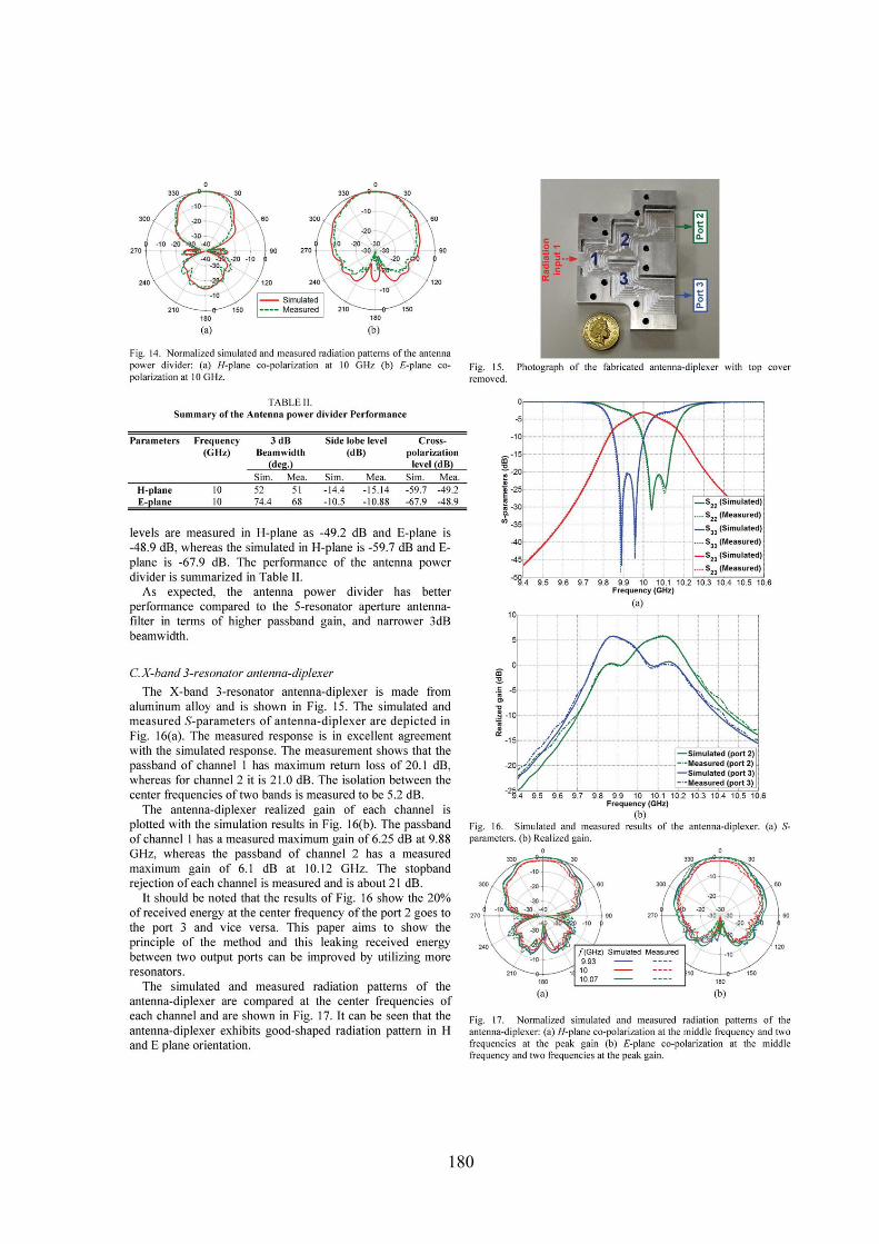
180
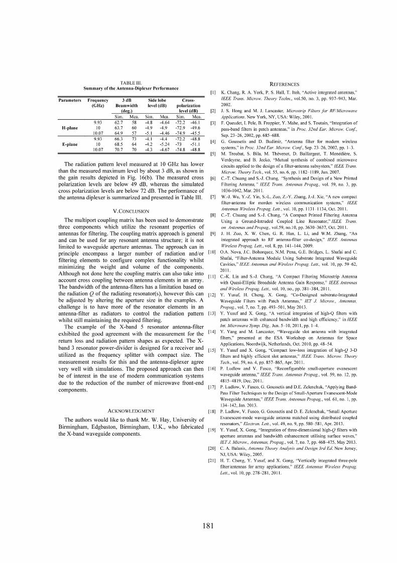
181
182