Embed Size (px)
Citation preview
©� Semiconductor Components Industries, LLC, 2008
February, 2008 - Rev. 31 Publication Order Number:
NCP1396/D
NCP1396A, NCP1396B
High Performance ResonantMode Controller featuringHigh-Voltage Drivers
The NCP1396 A/B offers everything needed to build a reliable andrugged resonant mode power supply. Its unique architecture includesa 500�kHz Voltage Controlled Oscillator whose control mode bringsflexibility when an ORing function is a necessity, e.g. in multiplefeedback paths implementations. Thanks to its proprietaryhigh-voltage technology, the controller welcomes a bootstrappedMOSFET driver for half-bridge applications accepting bulk voltagesup to 600�V. Protections featuring various reaction times, e.g.immediate shutdown or timer-based event, brown-out, brokenopto-coupler detection etc., contribute to a safer converter design,without engendering additional circuitry complexity. An adjustabledeadtime also helps lowering the shoot-through current contributionas the switching frequency increases.
Features
•�High-frequency Operation from 50 kHz up to 500 kHz
•�600 V High-Voltage Floating Driver•�Selectable Minimum Switching Frequency with ±3% Accuracy
•�Adjustable Deadtime from 100 ns to 2 �s.
•�Startup Sequence via an Adjustable Soft-start
•�Brown-out Protection for a Simpler PFC Association•�Latched Input for Severe Fault Conditions, e.g. Over Temperature
or OVP•�Timer-based Input with Auto-recovery Operation for Delayed
Event Reaction•�Enable Input for Immediate Event Reaction or Simple ON/OFF
Control•�VCC Operation up to 20 V•�Low Startup Current of 300 �A
•�1 A / 0.5 A Peak Current Sink / Source Drive Capability
•�Common Collector Optocoupler Connection for Easier ORing•�Internal Temperature Shutdown
•�B Version features 10 V VCC Startup Threshold
•�SO-16 or PDIP-16, Less Pin 13 Packages
Typical Applications
•�Flat Panel Display Power Converters
•�High Power AC/DC Adapters for Notebooks•�Industrial and Medical Power Sources
•�Offline Battery Chargers
PIN CONNECTIONS
http://onsemi.com
MARKINGDIAGRAMS
x = A or BA = Assembly LocationWL = Wafer LotYY, Y = YearWW = Work WeekG = Pb-Free Package
SO-16, LESS PIN 13D SUFFIX
CASE 751AM
1
16
1
2
3
4
5
6
7
8
16
15
14
12
11
10
9
(Top View)
BO
Css
Fmax
Ctimer
Rt
FB
DT
Fast Fault
Vboot
Mupper
Vcc
Mlower
Slow Fault
HB
Gnd
See detailed ordering and shipping information in the packagedimensions section on page 24 of this data sheet.
ORDERING INFORMATION
1
16
NCP1396xGAWLYWW
PDIP-16, LESS PIN 13P SUFFIX
CASE 626AB
16
1
NCP1396xAWLYYWWG16
1

NCP1396A, NCP1396B
http://onsemi.com2
Figure 1. Typical Application Example
C9
R19
C8
R9
C10
R7
R14 R18 R13
VoutL1
R23 D4
C6+M1
M2
R10
R11
T1
D1
D2
+
C13
C1
R16
D7
D9
C14
R21
Slow Input
C12
C7+D3 C11
R6
Soft-start
fmax
DTBOSkipSelection
Rt
OVPFB
U2A
FastInput
U5
D8
R20
R24R8R17
U3A
Timer
HV
R2
D6
C3
C4
U1
R3
U3BU2B
FB OVP
R12
R1R5C2
R4
R22
16
15
14
12
11
10
98
7
6
5
4
3
2
1
PIN FUNCTION DESCRIPTION
Pin No. Pin Name Function Pin Description
1 Css Soft-start Select the soft-start duration
2 Fmax Frequency clamp A resistor sets the maximum frequency excursion
3 Ctimer Timer duration Sets the timer duration in presence of a fault
4 Rt Timing resistor Connecting a resistor to this pin, sets the minimum oscillator frequencyreached for VFB = 1 V
5 BO Brown-Out Detects low input voltage conditions. When brought above Vlatch, it fullylatches off the controller.
6 FB Feedback Injecting current in this pin increases the oscillation frequency up to Fmax.
7 DT Dead-time A simple resistor adjusts the dead-time width
8 Fast Fault Quick fault detection Fast shut-down pin. Upon release, a clean startup sequence occurs. Can beused for skip cycle purposes.
9 Slow Fault Slow fault detection When asserted, the timer starts to countdown and shuts down the controllerat the end of its time duration.
10 Gnd Analog ground -
11 Mlower Low side output Drives the lower side MOSFET
12 Vcc Supplies the controller The controller accepts up to 20 V
13 - - -
14 HB Half-bridge connection Connects to the half-bridge output
15 Mupper High side output Drives the higher side MOSFET
16 Vboot Bootstrap pin The floating VCC supply for the upper stage
NCP1396A, NCP1396B
http://onsemi.com3
Vref
Rt
Vdd
C IDT
-+
+
DT Adj.
I = Imax for Vfb = 5.3 VI = 0 for Vfb < Vfb_min
Vref
Vdd
IminVfb ≤ Vfb_off
Vref
Vdd
ImaxVfb = 5
Fmax
Vdd
Itimer
If FAULT Itimer else 0
-+Timer
+Vref
PONResetFaultVdd
ISS
SS
FB
RFB
-+
+Vfb_fault
-+G = 1
> 0 onlyV = V(FB) - Vfb_min
IDT
Vref
Vdd
+
Vfb_min
DTDeadtime
AdjustmentVdd
-+BO
+VBO
-+
+Vlatch
20 �s NoiseFilter
Clk
D
S
Q
Q
R
S
Q Q
R PON Reset
50% DC
TemperatureShutdown
VC
CM
anagement
PONReset
Fault
TimeoutFault
Vref
BOReset
FF
+
-
+Vref Fault
FastFault
VCC
TimeoutFault
SS
Fault
Mlower
GND
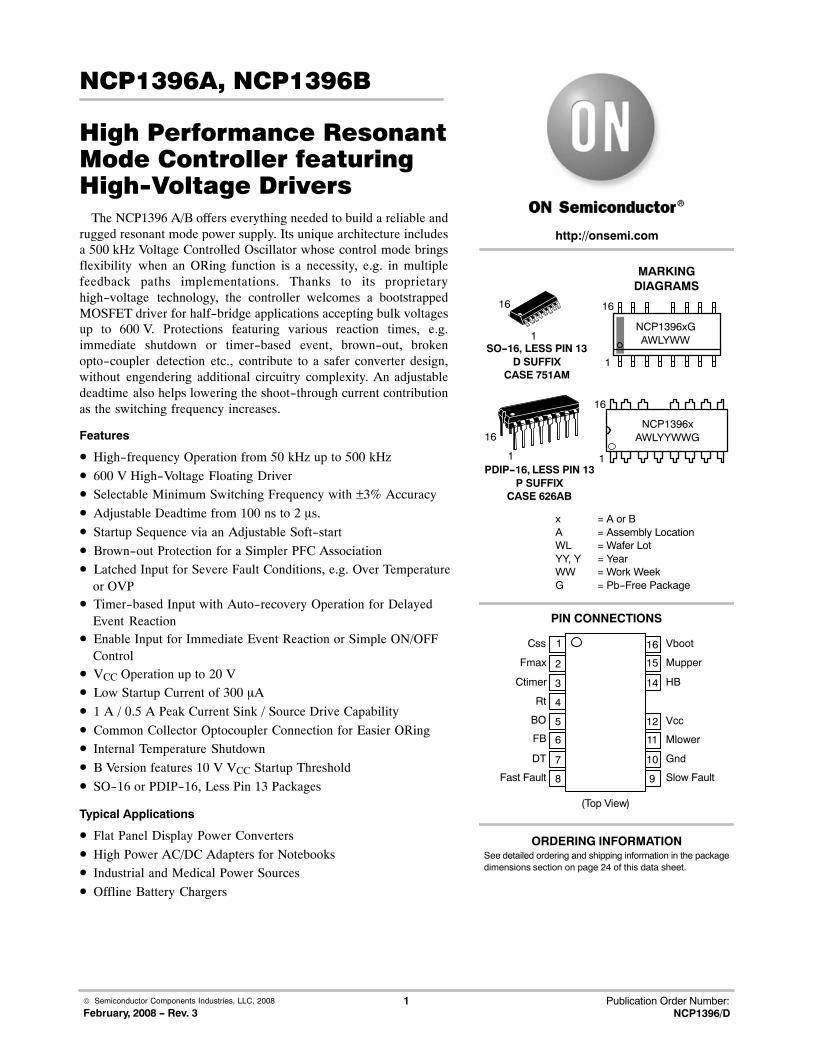
Figure 2. Internal Circuit Architecture
IBO20 �s Noise
Filter
20 ns NoiseFilter
+-Slow
Fault +Vref Fault
NC
VBOOT
Mupper
HB
UVLO
LevelShifter
FastFault

NCP1396A, NCP1396B
http://onsemi.com4
MAXIMUM RATINGS
Rating Symbol Value Unit
High Voltage bridge pin, pin 14 VBRIDGE -1 to 600 V
Floating supply voltage VBOOT-VBRIDGE
0 to 20 V
High side output voltage VDRV_HI VBRIDGE-0.3 toVBOOT+0.3
V
Low side output voltage VDRV_LO -0.3 to VCC + 0.3 V
Allowable output slew rate dVBRIDGE/dt 50 V/ns
Power Supply voltage, pin 12 Vcc 20 V
Maximum voltage, all pins (except pin 11 and 10) - -0.3 to 10 V
Thermal Resistance - Junction-to-Air, SOIC version RθJA 130 °C/W
Thermal Resistance - Junction-to-Air, PDIP version RθJA 100 °C/W
Operating Junction Temperature Range TJ -40 to +125 °C
Maximum Junction Temperature TJMAX +150 °C
Storage Temperature Range TSTG -60 to +150 °C
ESD Capability, HBM model (All pins except VCC and HV) - 2 kV
ESD Capability, Machine Model (All pins except pin 11 – see Note 1) - 200 V
Stresses exceeding Maximum Ratings may damage the device. Maximum Ratings are stress ratings only. Functional operation above theRecommended Operating Conditions is not implied. Extended exposure to stresses above the Recommended Operating Conditions may affectdevice reliability.1. This device series contains ESD protection and exceeds the following tests:
�Human Body Model 2000 V per Mil-Std-883, Method 3015�Machine Model Method 200 V�ESD Capability, Machine Model for pin 11 is 180 V.
2. This device meets latch-up tests defined by JEDEC Standard JESD78.

NCP1396A, NCP1396B
http://onsemi.com5
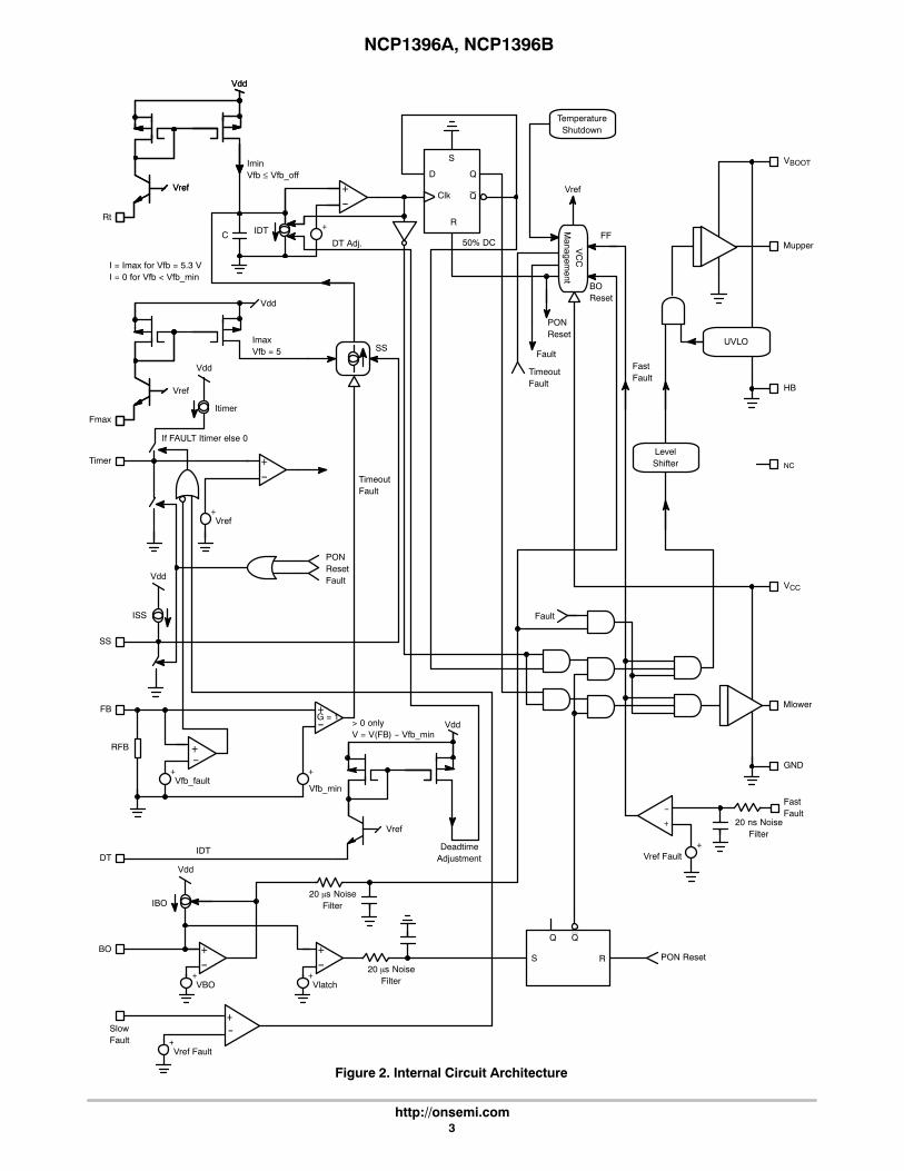
ELECTRICAL CHARACTERISTICS(For typical values TJ = 25°C, for min/max values TJ = -40°C to +125°C, Max TJ = 150°C, VCC = 12 V, unless otherwise noted.)
Characteristic Pin Symbol Min Typ Max Unit
SUPPLY SECTION
Turn-on threshold level, Vcc going up – A version 12 VCCON 12.3 13.4 14.3 V
Turn-on threshold level, Vcc going up – B version 12 VCCON 9.5 10.5 11.5 V
Minimum operating voltage after turn-on 12 VCC(min) 8.5 9.5 10.5 V
Startup voltage on the floating section 16-14 VbootON 8 9 10 V
Cutoff voltage on the floating section 16-14 Vboot(min) 7.4 8.4 9.4 V
Startup current, Vcc < VCCON 0°C < TJ < +125°C-40°C < TJ < +125°C
12 Istartup --
--
300350
�A
Vcc level at which the internal logic gets reset 12 VCCreset - 6.5 - V
Internal IC consumption, no output load on pin 15/14 – 11/10, Fsw =300�kHz
12 ICC1 - 4 - mA
Internal IC consumption, 1�nF output load on pin 15/14 – 11/10, Fsw =300�kHz
12 ICC2 - 11 - mA
Consumption in fault mode (All drivers disabled, VCC > VCC(min) ) 12 ICC3 - 1.2 - mA
VOLTAGE CONTROL OSCILLATOR (VCO)
Characteristic Pin Symbol Min Typ Max Unit
Minimum switching frequency, Rt = 18 k� on pin 4, Vpin 6 = 0.8 V, DT =300 ns
4 Fsw min 58.2 60 61.8 kHz
Maximum switching frequency, Rfmax = 1.3 k� on pin 2, Vpin 6 > 5.3 V,Rt = 18 k�, DT = 300 ns
2 Fsw max 425 500 575 kHz
Feedback pin swing above which Δf = 0 6 FBSW - 5.3 - V
Operating duty-cycle symetry 11-15 DC 48 50 52 %
Delay before any driver re-start in fault mode - Tdel - 20 - �s
FEEDBACK SECTION
Characteristic Pin Symbol Min Typ Max Unit
Internal pull-down resistor 6 Rfb - 20 - k�
Voltage on pin 6 below which the FB level has no VCO action 6 Vfb_min - 1.2 - V
Voltage on pin 6 below which the controller considers a fault 6 Vfb_off - 0.6 - V
DRIVE OUTPUT
Characteristic Pin Symbol Min Typ Max Unit
Output voltage rise-time @ CL = 1 nF, 10-90% of output signal 15-14/11-10
Tr - 40 - ns
Output voltage fall-time @ CL = 1 nF, 10-90% of output signal 15-14/11-10
Tf - 20 - ns
Source resistance 15-14/11-10
ROH - 13 - �
Sink resistance 15-14/11-10
ROL - 5.5 - �
Dead time with RDT = 10 k� from pin 7 to GND 7 T_dead 250 300 340 ns
Maximum dead-time with RDT = 82 k� from pin 7 to GND 7 T_dead-max - 2 - �s
Minimum dead-time, RDT = 3 k� from pin 7 to GND 7 T_dead-min - 100 - ns
Leakage current on high voltage pins to GND 14,15,16
IHV_LEAK - - 5 �A
NCP1396A, NCP1396B
http://onsemi.com6
ELECTRICAL CHARACTERISTICS(For typical values TJ = 25°C, for min/max values TJ = -40°C to +125°C, Max TJ = 150°C, VCC = 12 V, unless otherwise noted.)
TIMERS
Characteristic Pin Symbol Min Typ Max Unit
Timer charge current 3 Itimer - 160 - �A
Timer duration with a 1 �F capacitor and a 1 M� resistor 3 T-timer - 25 - ms
Timer recurrence in permanent fault, same values as above 3 T-timerR - 1.4 - s
Voltage at which pin 3 stops output pulses 3 VtimerON 3.5 4 4.4 V
Voltage at which pin 3 re-starts output pulses 3 VtimerOFF 0.9 1 1.1 V
Soft-start ending voltage 1 VSS - 2 - V
Soft-start charge current 0°C < TJ < +125°C-40°C < TJ < +125°C
1 ISS 8075
110110
125130
�A
Soft-start duration with a 100 nF capacitor (Note 3) 1 T-SS - 1.8 - ms
PROTECTION
Characteristic Pin Symbol Min Typ Max Unit
Reference voltage for fast input (Note 4) 8-9 VrefFaultF 1.00 1.05 1.10 V
Hysteresis for fast input (Note 4) 8-9 HysteFaultF - 80 - mV
Reference voltage for slow input 0°C < TJ < +125°C-40°C < TJ < +125°C
8-9 VrefFaultS 0.950.92
1.001.00
1.051.05
V
Hysteresis for slow input 8-9 HysteFaultS - 60 - mV
Propagation delay for fast fault input drive shutdown 8 TpFault - 55 90 ns
Brown-Out input bias current 5 IBObias - 0.02 - �A
Brown-Out level (Note 4) 5 VBO 0.99 1.04 1.09 V
Hysteresis current, Vpin5 > VBO – A version 0°C < TJ < +125°C-40°C < TJ < +125°C
5 IBO_A 21.519
26.5 26.5
31.5 33
�A
Hysteresis current, Vpin5 > VBO – B version 0°C < TJ < +125°C-40°C < TJ < +125°C
5 IBO_B 8680
106106
126132
�A
Latching voltage 5 Vlatch 3.6 4 4.4 V
Temperature shutdown - TSD 140 - - °C
Hysteresis - TSDhyste - 30 - °C
3. The A version does not activate soft-start (unless the feedback pin voltage is below 0.6 V) when the fast-fault is released, this is for skip cycleimplementation. The B version does activate the soft-start upon release of the fast-fault input for any feedback conditions.
4. Guaranteed by design
NCP1396A, NCP1396B
http://onsemi.com7
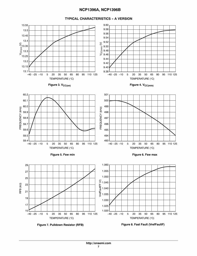
TYPICAL CHARACTERISTICS - A VERSION
Figure 3. VCC(on) Figure 4. VCC(min)
Figure 5. Fsw min Figure 6. Fsw max
Figure 7. Pulldown Resistor (RFB)
13.1
13.15
13.2
13.3
13.4
13.5
-40 5 50
VC
C(o
n) (
V)
TEMPERATURE (°C)
125-10 35 80-25 20 65
9.58
9.60
9.42
9.48
9.52
9.56
-40 5 50
VC
C(m
in) (
V)
TEMPERATURE (°C)
125-10 35 110-25 20 95
59.4
59.6
59.8
60.0
60.2
-40 5 65
FR
EQ
UE
NC
Y (
kHz)
TEMPERATURE (°C)
125-10 50 110-25 20 95493
495
497
499
501
-40 5 65
FR
EQ
UE
NC
Y (
kHz)
TEMPERATURE (°C)
125-10 35 110-25 20 95
15
17
19
21
27
29
-40 5 65
RF
B (
k�)
TEMPERATURE (°C)
125-10 50 110-25 20 951.020
1.030
1.040
1.050
1.060
-40 5 65
Vre
fFau
ltFF
(V
)
TEMPERATURE (°C)
125-10 50 110-25 20 95
95 110 65 809.38
9.40
9.46
9.44
9.50
9.54
35 80
59.5
59.7
59.9
60.1
50 80
494
496
498
500
23
25
35 80 35 80
1.025
1.035
1.045
1.055
Figure 8. Fast Fault (VrefFaultF)
13.25
13.35
13.45
13.55
NCP1396A, NCP1396B
http://onsemi.com8
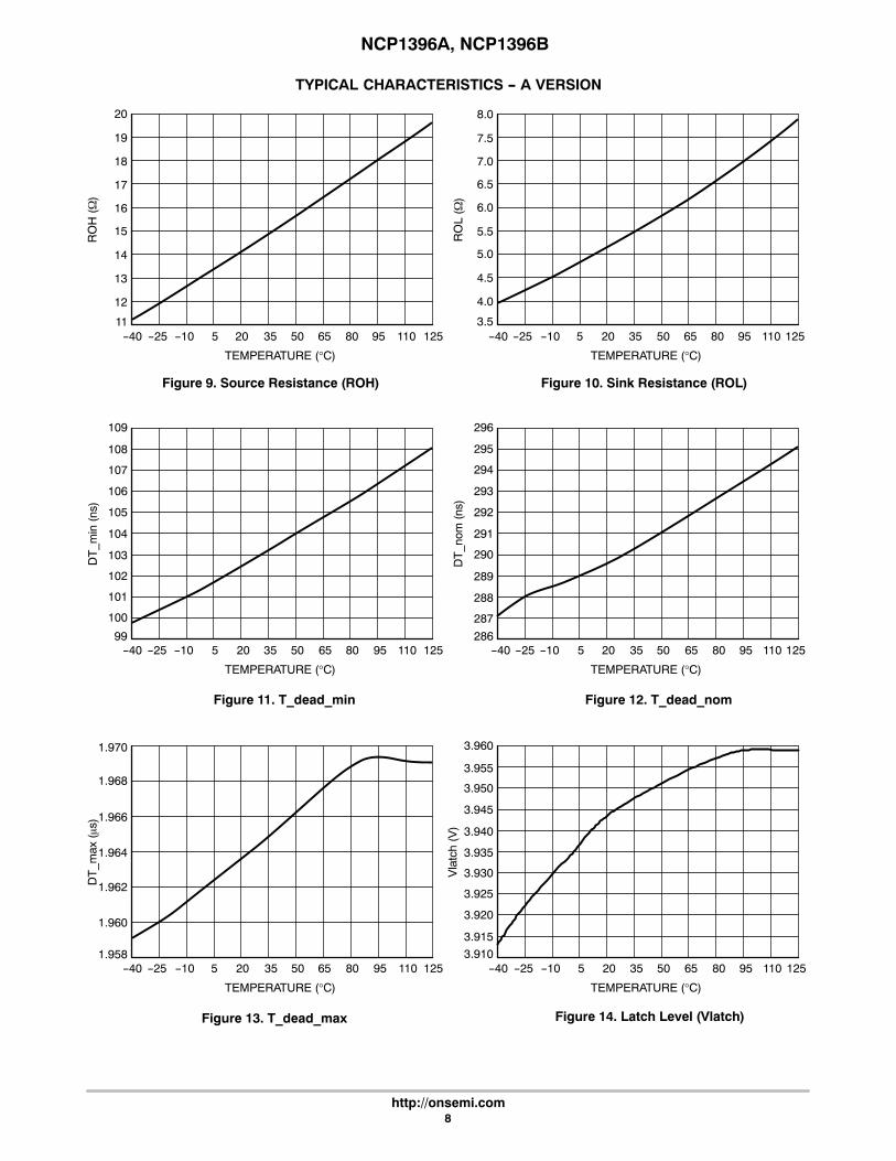
TYPICAL CHARACTERISTICS - A VERSION
Figure 9. Source Resistance (ROH) Figure 10. Sink Resistance (ROL)
Figure 11. T_dead_min Figure 12. T_dead_nom
Figure 13. T_dead_max
11
12
13
16
18
20
-40 5 50
RO
H (�
)
TEMPERATURE (°C)
125-10 35 80-25 20 653.5
4.0
5.0
7.0
8.0
-40 5 50
RO
L (�
)
TEMPERATURE (°C)
125-10 35 110-25 20 95
99
101
104
106
109
-40 5 65
DT
_min
(ns
)
TEMPERATURE (°C)
125-10 50 110-25 20 95286
288
290
292
296
-40 5 65
DT
_nom
(ns
)
TEMPERATURE (°C)
125-10 35 110-25 20 95
1.958
1.960
1.962
1.968
1.970
-40 5 65
DT
_max
(�s)
TEMPERATURE (°C)
125-10 50 110-25 20 953.910
3.920
3.930
3.950
3.960
-40 5 65
Vla
tch
(V)
TEMPERATURE (°C)
125-10 50 110-25 20 95
95 110 65 80
4.5
6.0
5.5
6.5
7.5
35 80
100
102
105
108
50 80
287
289
291
295
1.964
1.966
35 80 35 80
3.915
3.925
3.940
3.955
Figure 14. Latch Level (Vlatch)
14
15
17
19
103
107
293
294
3.935
3.945

NCP1396A, NCP1396B
http://onsemi.com9
TYPICAL CHARACTERISTICS - A VERSION
Figure 15. Brown-Out Reference (VBO) Figure 16. Brown-Out Hysteresis Current (IBO)
1.020
1.025
1.045
-40 5 50
VB
O (
V)
TEMPERATURE (°C)
125-10 35 80-25 20 6525.0
25.2
25.6
26.4
26.8
-40 5 50
IBO
(�A
)
TEMPERATURE (°C)
125-10 35 110-25 20 9595 110 65 80
25.4
26.0
25.8
26.2
26.6
1.030
1.035
1.040
NCP1396A, NCP1396B
http://onsemi.com10
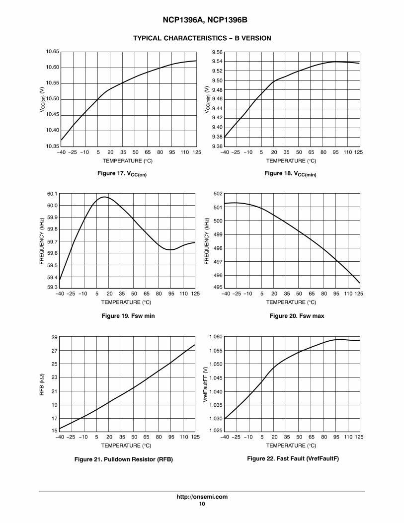
TYPICAL CHARACTERISTICS - B VERSION
Figure 17. VCC(on) Figure 18. VCC(min)
Figure 19. Fsw min Figure 20. Fsw max
Figure 21. Pulldown Resistor (RFB)
10.65
10.35
10.40
10.50
10.55
10.60
-40 5 50
VC
C(o
n) (
V)
TEMPERATURE (°C)
125-10 35 80-25 20 659.36
9.42
9.48
9.52
9.56
-40 5 50
VC
C(m
in) (
V)
TEMPERATURE (°C)
125-10 35 110-25 20 95
59.4
59.6
59.8
60.0
-40 5 65
FR
EQ
UE
NC
Y (
kHz)
TEMPERATURE (°C)
125-10 50 110-25 20 95495
497
499
501
-40 5 65
FR
EQ
UE
NC
Y (
kHz)
TEMPERATURE (°C)
125-10 35 110-25 20 95
15
17
19
21
27
29
-40 5 65
RF
B (
k�)
TEMPERATURE (°C)
125-10 50 110-25 20 95
1.030
1.040
1.050
1.060
-40 5 65
Vre
fFau
ltFF
(V
)
TEMPERATURE (°C)
125-10 50 110-25 20 95
95 110 65 80
9.38
9.40
9.46
9.44
9.50
9.54
35 80
59.5
59.7
59.9
60.1
50 80
496
498
500
23
25
35 80 35 801.025
1.035
1.045
1.055
Figure 22. Fast Fault (VrefFaultF)
10.45
59.3
502

NCP1396A, NCP1396B
http://onsemi.com11
TYPICAL CHARACTERISTICS - B VERSION
Figure 23. Source Resistance (ROH) Figure 24. Sink Resistance (ROL)
Figure 25. T_dead_min Figure 26. T_dead_nom
Figure 27. T_dead_max
11
12
13
16
18
-40 5 50
RO
H (�
)
TEMPERATURE (°C)
125-10 35 80-25 20 653.5
4.0
5.0
7.0
8.0
-40 5 50
RO
L (�
)
TEMPERATURE (°C)
125-10 35 110-25 20 95
99
101
104
106
-40 5 65
DT
_min
(ns
)
TEMPERATURE (°C)
125-10 50 110-25 20 95
286
288
290
292
-40 5 65
DT
_nom
(ns
)
TEMPERATURE (°C)
125-10 35 110-25 20 95
1.958
1.960
1.962
1.968
1.970
-40 5 65
DT
_max
(�s)
TEMPERATURE (°C)
125-10 50 110-25 20 953.930
3.940
3.950
3.970
3.980
-40 5 65
Vla
tch
(V)
TEMPERATURE (°C)
125-10 50 110-25 20 95
95 110 65 80
4.5
6.0
5.5
6.5
7.5
35 80
100
102
105
108
50 80
287
289
291
1.964
1.966
35 80 35 80
3.935
3.945
3.960
3.975
Figure 28. Latch Level (Vlatch)
14
15
17
19
103
107 293
294
3.955
3.965
10
284
285
98

NCP1396A, NCP1396B
http://onsemi.com12
TYPICAL CHARACTERISTICS - B VERSION
Figure 29. Brown-Out Reference (VBO) Figure 30. Brown-Out Hysteresis Current (IBO)
1.025
1.045
-40 5 50
VB
O (
V)
TEMPERATURE (°C)
125-10 35 80-25 20 6599
100
105
107
-40 5 50
IBO
(�A
)
TEMPERATURE (°C)
125-10 35 110-25 20 9595 110 65 80
101
103
102
104
106
1.030
1.035
1.040
1.050

NCP1396A, NCP1396B
http://onsemi.com13
Application Information
The NCP1396 A/B includes all necessary features to helpbuilding a rugged and safe switch-mode power supplyfeaturing an extremely low standby power. The belowbullets detail the benefits brought by implementing theNCP1396 controller:• Wide frequency range: A high-speed Voltage
Control Oscillator allows an output frequencyexcursion from 50�kHz up to 500 kHz on Mlower andMupper outputs.
• Adjustable dead-time: Thanks to a single resistorwired to ground, the user has the ability to includesome dead-time, helping to fight cross-conductionbetween the upper and the lower transistor.
• Adjustable soft-start: Every time the controller startsto operate (power on), the switching frequency ispushed to the programmed maximum value and slowlymoves down toward the minimum frequency, until thefeedback loop closes. The soft-start sequence isactivated in the following cases: a) normal startupb)�back to operation from an off state: during hiccupfaulty mode, brown-out or temperature shutdown(TSD). In the NCP1396A, the soft-start is notactivated back to operation from the fast fault input,unless the feedback pin voltage is below 0.6 V. To theopposite, in the B version, the soft-start is alwaysactivated back from the fast fault input whatever thefeedback level is.
• Adjustable minimum and maximum frequencyexcursion: In resonant applications, it is important tostay away from the resonating peak to keep operatingthe converter in the right region. Thanks to a singleexternal resistor, the designer can program its lowestfrequency point, obtained in lack of feedback voltage(during the startup sequence or in short-circuitconditions). Internally trimmed capacitors offer a ±3%precision on the selection of the minimum switchingfrequency. The adjustable upper stop being lessprecise to ±15%.
• Low startup current: When directly powered fromthe high-voltage DC rail, the device only requires300��A to start-up. In case of an auxiliary supply, theB version offers a lower start-up threshold to copewith a 12 V dc rail.
• Brown-Out detection: To avoid operation from a lowinput voltage, it is interesting to prevent the controllerfrom switching if the high-voltage rail is not withinthe right boundaries. Also, when teamed with a PFCfront-end circuitry, the brown-out detection canensure a clean start-up sequence with soft-start,ensuring that the PFC is stabilized before energizingthe resonant tank. The A version features a 26.5 �Ahysteresis current for the lowest consumption and the
B version slightly increases this current to 100 �A inorder to improve the noise immunity.
• Adjustable fault timer duration: When a fault isdetected on the slow fault input or when the FB path isbroken, a timer starts to charge an external capacitor.If the fault is removed, the timer opens the chargingpath and nothing happens. When the timer reaches itsselected duration (via a capacitor on pin 3), all pulsesare stopped. The controller now waits for thedischarge via an external resistor of pin 3 capacitor toissue a new clean startup sequence with soft-start.
• Cumulative fault events: In the NCP1396A/B, thetimer capacitor is not reset when the fault disappears.It actually integrates the information and cumulatesthe occurrences. A resistor placed in parallel with thecapacitor will offer a simple way to adjust thedischarge rate and thus the auto-recovery retry rate.
• Fast and slow fault detection: In some application,subject to heavy load transients, it is interesting togive a certain time to the fault circuit, beforeactivating the protection. On the other hands, somecritical faults cannot accept any delay before acorrective action is taken. For this reason, theNCP1396A/B includes a fast fault and a slow faultinput. Upon assertion, the fast fault immediately stopsall pulses and stays in the position as long as thedriving signal is high. When released low (the faulthas gone), the controller has several choices: in the Aversion, pulses are back to a level imposed by thefeedback pin without soft-start, but in the B version,pulses are back through a regular soft-start sequence.
• Skip cycle possibility: The absence of soft-start onthe NCP1396A fast fault input offers an easy way toimplement skip cycle when power saving features arenecessary. A simple resistive connection from thefeedback pin to the fast fault input, and skip can beimplemented.
• Broken feedback loop detection: Upon start-up orany time during operation, if the FB signal is missing,the timer starts to charge a capacitor. If the loop isreally broken, the FB level does not grow-up beforethe timer ends counting. The controller then stops allpulses and waits that the timer pin voltage collapses to1�V typically before a new attempt to re-start, via thesoft-start. If the optocoupler is permanently broken, ahiccup takes place.
• Finally, two circuit versions, A and B: The A and Bversions differ because of the following changes:
1. The startup thresholds are different, the A startsto pulse for VCC = 13.3 V whereas the B pulsesfor VCC = 10.5 V. The turn off levels are the samehowever. The A is recommended for consumer
NCP1396A, NCP1396B
http://onsemi.com14
products where the designer can use an externalstartup resistor, whereas the B is morerecommended for industrial / medicalapplications where a 12 V auxiliary supplydirectly powers the chip.
2. The A version does not activate the soft-startupon release of the fast fault input. This is to letthe designer implement skip cycle. To theopposite, the B version goes back to operationupon the fast fault pin release via a soft-startsequence.
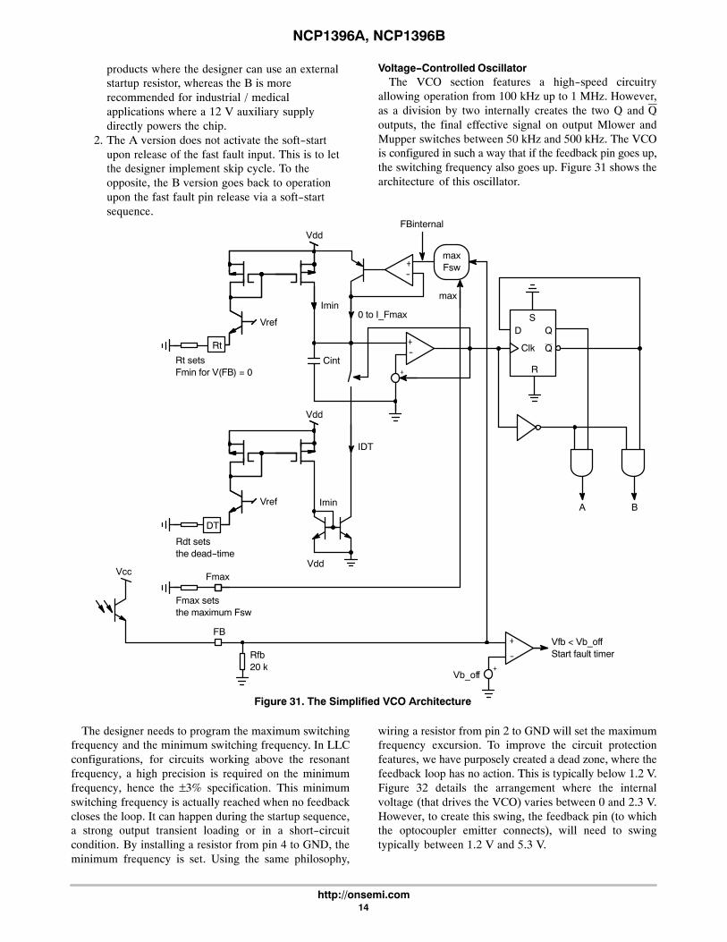
Voltage-Controlled OscillatorThe VCO section features a high-speed circuitry
allowing operation from 100 kHz up to 1 MHz. However,as a division by two internally creates the two Q and Qoutputs, the final effective signal on output Mlower andMupper switches between 50 kHz and 500 kHz. The VCOis configured in such a way that if the feedback pin goes up,the switching frequency also goes up. Figure 31 shows thearchitecture of this oscillator.
Figure 31. The Simplified VCO Architecture
Vref
Vdd
Rt setsFmin for V(FB) = 0
Cint
Imin
+-
0 to I_Fmax
IDT
FBinternal
maxFsw
max
+-
+
Clk
DS
Q
Q
R
A BVref
Vdd
Rdt setsthe dead-time
DT
Imin
VddFmax
Fmax setsthe maximum Fsw
Vcc
FB
Rfb20 k
+
-+
Vfb < Vb_offStart fault timer
Vb_off
Rt
The designer needs to program the maximum switchingfrequency and the minimum switching frequency. In LLCconfigurations, for circuits working above the resonantfrequency, a high precision is required on the minimumfrequency, hence the ±3% specification. This minimumswitching frequency is actually reached when no feedbackcloses the loop. It can happen during the startup sequence,a strong output transient loading or in a short-circuitcondition. By installing a resistor from pin 4 to GND, theminimum frequency is set. Using the same philosophy,
wiring a resistor from pin 2 to GND will set the maximumfrequency excursion. To improve the circuit protectionfeatures, we have purposely created a dead zone, where thefeedback loop has no action. This is typically below 1.2�V.Figure 32 details the arrangement where the internalvoltage (that drives the VCO) varies between 0 and 2.3�V.However, to create this swing, the feedback pin (to whichthe optocoupler emitter connects), will need to swingtypically between 1.2 V and 5.3 V.

NCP1396A, NCP1396B
http://onsemi.com15
Figure 32. The OPAMP Arrangement Limits theVCO Modulation Signal between 0.5 and 2.3 V
VCC
FB
R111.3 k
-+
+
Vref0.5 VR2
8.7 k
R3100 k
D12.3 V
Rfmax
Fmax
This techniques allows us to detect a fault on theconverter in case the FB pin cannot rise above 0.6�V (toactually close the loop) in less than a duration imposed bythe programmable timer. Please refer to the fault section fordetailed operation of this mode.
As shown on Figure 32, the internal dynamics of theVCO control voltage will be constrained between 0.5�Vand 2.3�V, whereas the feedback loop will drive pin 6 (FB)between 1.2�V and 5.3�V. If we take the default FB pinexcursion numbers, 1.2�V = 50�kHz, 5.3�V = 500�kHz, thenthe VCO maximum slope will be:
500�k � 50�k4.1
� 109.7�kHz�V
Figures 33 and 34 portray the frequency evolutiondepending on the feedback pin voltage level in a differentfrequency clamp combination.
Figure 33. Maximal Default Excursion, Rt =22�k� on pin 4 and Rfmax = 1.3 k� on pin 2
VFB
FMu&Lu
1.2 V 5.3 V
Fmin
Fmax
Faultarea
No variations
50 kHz
500 kHz
0.6 V
�Fsw = 450 kHz
�VFB = 4.1 V
Figure 34. Here a different minimum frequency wasprogrammed as well as a maximum frequency
excursion
VFB
FMu&Lu
1.2 V 5.3 V
Fmin
Fmax
Faultarea
No variations
150 kHz
450 kHz
0.6 V
�Fsw = 300 kHz
�VFB = 4.1 V
Please note that the previous small-signal VCO slope hasnow been reduced to 300 k / 4.1 = 73 kHz / V on Mupperand Mlower outputs. This offers a mean to magnify thefeedback excursion on systems where the load range doesnot generate a wide switching frequency excursion. Thanksto this option, we will see how it becomes possible toobserve the feedback level and implement skip cycle atlight loads. It is important to note that the frequencyevolution does not have a real linear relationship with thefeedback voltage. This is due to the deadtime presencewhich stays constant as the switching period changes.
The selection of the three setting resistors (Fmax, Fmindeadtime) requires the usage of the selection chartsdisplayed below:
50
150
250
350
450
550
650
1.5 3.5 5.5 7.5 9.5 11.5 13.5 15.5 17.5
Fm
ax (
kHz)
Fmin = 50 kHz
Fmin = 200 kHz
Figure 35. Maximum Switching Frequency ResistorSelection Depending on the Adopted Minimum
Switching Frequency
RFmax (k�)
Vcc = 12 VFB = 6.5 VDT = 300 ns

NCP1396A, NCP1396B
http://onsemi.com16
100
150
200
250
300
350
400
450
500
1 3 5 7 9 11
Fm
in (
kHz)
Figure 36. Minimum Switching Frequency ResistorSelection (Fmin = 100 kHz to 500 kHz)
Vcc = 12 VFB = 1 VDT = 300 ns
RFmin (k�)
20
30
40
50
60
70
80
90
100
10 15 20 25 30 35 40 45 50 55
Fm
in (
kHz)
Figure 37. Minimum Switching Frequency ResistorSelection (Fmin = 20 kHz to 100 kHz)
Vcc = 12 VFB = 1 VDT = 300 ns
RFmin (k�)
100200300400500600700800900
10001100120013001400150016001700180019002000
3.5 13.5 23.5 33.5 43.5 53.5 63.5 73.5 83.5
Vcc = 12 V
Figure 38. Dead-Time Resistor Selection
DT
(ns
)
Rdt (k�)
ORing CapabilityIf for any particular reason, there is a need for a
frequency variation linked to an event appearance (insteadof abruptly stopping pulses), then the FB pin lends itselfvery well to the addition of other sweeping loops. Severaldiodes can easily be used perform the job in case of reactionto a fault event or to regulate on the output current (CCoperation). Figure 39 shows how to do it.
Figure 39. Thanks to the FB Configuration, LoopORing is Easy to Implement
VCC
FBIn1
In220 k
VCO
Dead-time ControlDead-time control is an absolute necessity when the
half-bridge configuration comes to play. The dead-timetechnique consists in inserting a period during which bothhigh and low side switches are off. Of course, thedead-time amount differs depending on the switchingfrequency, hence the ability to adjust it on this controller.The option ranges between 100 ns and 2 �s. The dead-timeis actually made by controlling the oscillator dischargecurrent. Figure 40 portrays a simplified VCO circuit basedon Figure 31.

NCP1396A, NCP1396B
http://onsemi.com17
Figure 40. Dead-time Generation
Vdd
Icharge:Fsw min + Fsw max
Idis
Ct
RDT
DT
Vref
+ 3 V-1 V
-
+Clk
DS
Q
Q
R
A B
NCP1396A, NCP1396B
http://onsemi.com18
During the discharge time, the clock comparator is highand un-validates the AND gates: both outputs are low.When the comparator goes back to the low level, during thetiming capacitor Ct recharge time, A and B outputs arevalidated. By connecting a resistor RDT to ground, itcreates a current whose image serves to discharge the Ctcapacitor: we control the dead-time. The typical rangeevolves between 100 ns (RDT = 3.5 k�) and 2 �s (RDT =83.5�k�). Figure 43 shows the typical waveforms.
Soft-start SequenceIn resonant controllers, a soft-start is needed to avoid
suddenly applying the full current into the resonatingcircuit. In this controller, a soft-start capacitor connects topin 1 and offers a smooth frequency variation uponstart-up: when the circuit starts to pulse, the VCO is pushedto the maximum switching frequency imposed by pin 2.Then, it linearly decreases its frequency toward theminimum frequency selected by a resistor on pin 4. Ofcourse, practically, the feedback loop is suppose to take
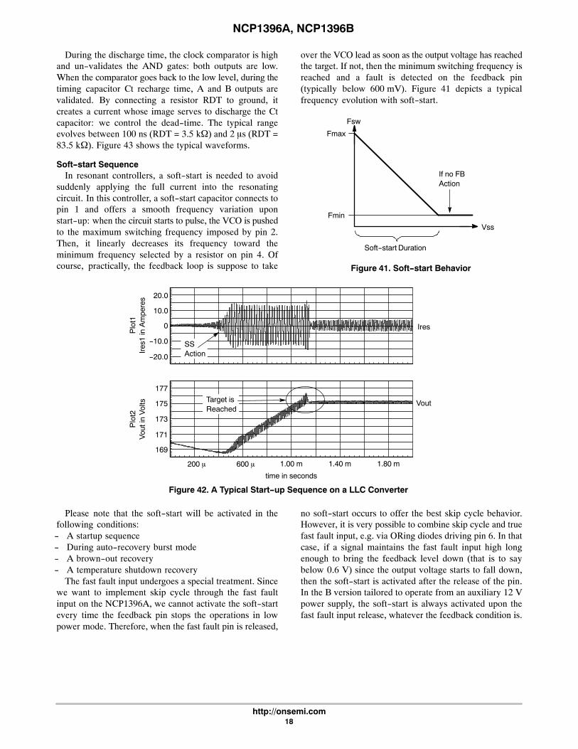
over the VCO lead as soon as the output voltage has reachedthe target. If not, then the minimum switching frequency isreached and a fault is detected on the feedback pin(typically below 600�mV). Figure 41 depicts a typicalfrequency evolution with soft-start.
Figure 41. Soft-start Behavior
Fsw
Fmax
Fmin
Vss
Soft-start Duration
If no FBAction
-20.0
-10.0
0
10.0
20.0
1.00 m 1.40 m 1.80 m
time in seconds
169
171
173
175
177
Figure 42. A Typical Start-up Sequence on a LLC Converter
Ires
Vout
600 �200 �
SSAction
Target isReached
Plo
t2V
out i
n V
olts
Plo
t1Ir
es1
in A
mpe
res
Please note that the soft-start will be activated in thefollowing conditions:- A startup sequence- During auto-recovery burst mode- A brown-out recovery- A temperature shutdown recovery
The fast fault input undergoes a special treatment. Sincewe want to implement skip cycle through the fast faultinput on the NCP1396A, we cannot activate the soft-startevery time the feedback pin stops the operations in lowpower mode. Therefore, when the fast fault pin is released,
no soft-start occurs to offer the best skip cycle behavior.However, it is very possible to combine skip cycle and truefast fault input, e.g. via ORing diodes driving pin 6. In thatcase, if a signal maintains the fast fault input high longenough to bring the feedback level down (that is to saybelow 0.6 V) since the output voltage starts to fall down,then the soft-start is activated after the release of the pin.In the B version tailored to operate from an auxiliary 12�Vpower supply, the soft-start is always activated upon thefast fault input release, whatever the feedback condition is.

NCP1396A, NCP1396B
http://onsemi.com19
0
1.00
2.00
3.00
4.00
0
4.00
8.00
12.0
16.0
time in seconds
-8.00
-4.00
0
4.00
8.00
Figure 43. Typical Oscillator Waveforms
Ct Voltage
56.2 � 65.9 � 75.7 � 85.4 � 95.1 �
Plo
t3D
iffer
ence
in V
olts
Plo
t2C
lock
in V
olts
Plo
t1V
ct in
Vol
ts
Clock Pulses DT
DTDT
A - B
Brown-Out ProtectionThe Brown-Out circuitry (BO) offers a way to protect the
resonant converter from low DC input voltages. Below agiven level, the controller blocks the output pulses, aboveit, it authorizes them. The internal circuitry, depicted byFigure�44, offers a way to observe the high-voltage (HV)rail. A resistive divider made of Rupper and Rlower, bringsa portion of the HV rail on pin 5. Below the turn-on level,the 26.5��A current source IBO is off. Therefore, theturn-on level solely depends on the division ratio broughtby the resistive divider.
Figure 44. The Internal Brown-out Configuration withan Offset Current Source
Vdd
+VBO
-
+
ON/OFFIBO
BO
Vbulk
Rupper
Rlower
BO
NCP1396A, NCP1396B
http://onsemi.com20
time in seconds
0
4.0
8.0
12.0
16.0
50
150
250
350
450
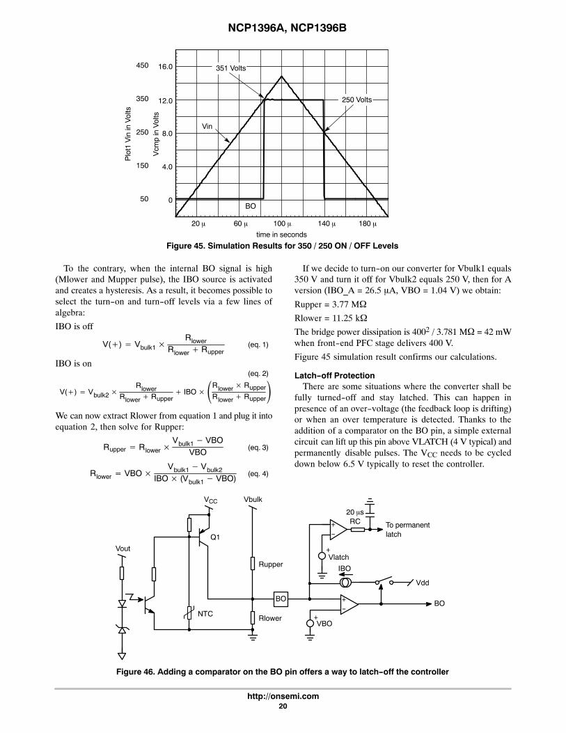
Figure 45. Simulation Results for 350 / 250 ON / OFF Levels
20 � 60 � 100 � 140 � 180 �
Vin
250 Volts
351 Volts
BO
Plo
t1 V
in in
Vol
ts
Vcm
p in
Vol
ts
To the contrary, when the internal BO signal is high(Mlower and Mupper pulse), the IBO source is activatedand creates a hysteresis. As a result, it becomes possible toselect the turn-on and turn-off levels via a few lines ofalgebra:
IBO is off
V(�) � Vbulk1 �Rlower
Rlower � Rupper(eq. 1)
IBO is on
V(�) � Vbulk2 �Rlower
Rlower � Rupper� IBO ��Rlower � Rupper
Rlower � Rupper�
(eq. 2)
We can now extract Rlower from equation 1 and plug it intoequation 2, then solve for Rupper:
Rupper � Rlower �Vbulk1 � VBO
VBO(eq. 3)
Rlower � VBO �Vbulk1 � Vbulk2
IBO � (Vbulk1 � VBO)(eq. 4)
If we decide to turn-on our converter for Vbulk1 equals350�V and turn it off for Vbulk2 equals 250�V, then for Aversion (IBO_A = 26.5 �A, VBO = 1.04 V) we obtain:
Rupper = 3.77 M�
Rlower = 11.25 k�
The bridge power dissipation is 4002 / 3.781�M� = 42�mWwhen front-end PFC stage delivers 400�V.
Figure 45 simulation result confirms our calculations.
Latch-off ProtectionThere are some situations where the converter shall be
fully turned-off and stay latched. This can happen inpresence of an over-voltage (the feedback loop is drifting)or when an over temperature is detected. Thanks to theaddition of a comparator on the BO pin, a simple externalcircuit can lift up this pin above VLATCH (4�V typical) andpermanently disable pulses. The VCC needs to be cycleddown below 6.5�V typically to reset the controller.
Figure 46. Adding a comparator on the BO pin offers a way to latch-off the controller
-+
20 �sRC To permanent
latch
+Vlatch
Vdd
-+
BO
+VBO
BO
Rlower
Rupper
VbulkVCC
Q1
NTC
Vout
IBO

NCP1396A, NCP1396B
http://onsemi.com21
On Figure 46, Q1 is blocked and does not bother the BOmeasurement as long as the NTC and the optocoupler arenot activated. As soon as the secondary optocoupler sensesan OVP condition, or the NTC reacts to a high ambienttemperature, Q1 base is brought to ground and the BO pingoes up, permanently latching off the controller.
Protection CircuitryThis resonant controller differs from competitors thanks
to its protection features. The device can react to variousinputs like:- Fast events input: like an over-current condition, a
need to shut down (sleep mode) or a way to force acontrolled burst mode (skip cycle at low outputpower): as soon as the input level exceeds 1�V typical,
pulses are immediately stopped. When the input isreleased, the controller performs a clean startupsequence including a soft-start period.
- Slow events input: this input serves as a delayedshutdown, where an event like a transient overloaddoes not immediately stopped pulses but start a timer.If the event duration lasts longer than what the timerimposes, then all pulses are disabled. The voltage onthe timer capacitor (pin 3) starts to decrease until itreaches 1�V. The decrease rate is actually dependingon the resistor the user will put in parallel with thecapacitor, giving another flexibility during design.
Figure 47 depicts the architecture of the fault circuitry.
Figure 47. This circuit combines a slow and fast input for improved protection features
Vdd
Itimer
ResetUVLORtimer
CtimerCtimer
+-
ON/OFF
1 = fault0 = ok
+Vref Fault
+ -
+
VtimerONVtimerOFF
1 = ok0 = fault
+-
Vref Fault
Fast Fault
+
1 = ok0 = fault
DRIVINGLOGIC
SS
A A
B B
Reset
Slow Fault
AverageInput
Current
To PrimaryCurrent SensingCircuitry
FB
Skip
Vcc
FB
Slow InputOn this circuit, the slow input goes to a comparator.
When this input exceeds 1�V typical, the current sourceItimer turns on, charging the external capacitor Ctimer. Ifthe fault duration is long enough, when Ctimer voltage
NCP1396A, NCP1396B
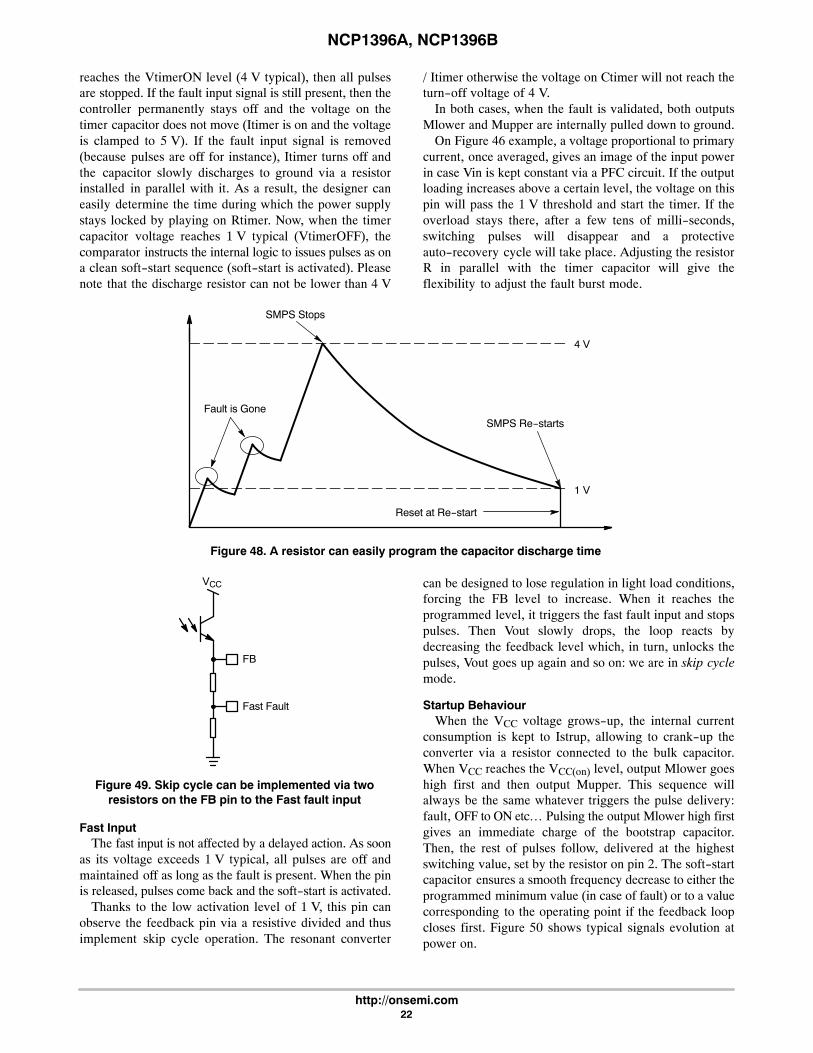
http://onsemi.com22
reaches the VtimerON level (4�V typical), then all pulsesare stopped. If the fault input signal is still present, then thecontroller permanently stays off and the voltage on thetimer capacitor does not move (Itimer is on and the voltageis clamped to 5�V). If the fault input signal is removed(because pulses are off for instance), Itimer turns off andthe capacitor slowly discharges to ground via a resistorinstalled in parallel with it. As a result, the designer caneasily determine the time during which the power supplystays locked by playing on Rtimer. Now, when the timercapacitor voltage reaches 1�V typical (VtimerOFF), thecomparator instructs the internal logic to issues pulses as ona clean soft-start sequence (soft-start is activated). Pleasenote that the discharge resistor can not be lower than 4�V
/ Itimer otherwise the voltage on Ctimer will not reach theturn-off voltage of 4�V.
In both cases, when the fault is validated, both outputsMlower and Mupper are internally pulled down to ground.
On Figure 46 example, a voltage proportional to primarycurrent, once averaged, gives an image of the input powerin case Vin is kept constant via a PFC circuit. If the outputloading increases above a certain level, the voltage on thispin will pass the 1�V threshold and start the timer. If theoverload stays there, after a few tens of milli-seconds,switching pulses will disappear and a protectiveauto-recovery cycle will take place. Adjusting the resistorR in parallel with the timer capacitor will give theflexibility to adjust the fault burst mode.
Figure 48. A resistor can easily program the capacitor discharge time
4 V
1 V
SMPS Re-starts
SMPS Stops
Reset at Re-start
Fault is Gone
Fast Fault
FB
VCC
Figure 49. Skip cycle can be implemented via tworesistors on the FB pin to the Fast fault input
Fast InputThe fast input is not affected by a delayed action. As soon
as its voltage exceeds 1�V typical, all pulses are off andmaintained off as long as the fault is present. When the pinis released, pulses come back and the soft-start is activated.
Thanks to the low activation level of 1�V, this pin canobserve the feedback pin via a resistive divided and thusimplement skip cycle operation. The resonant converter
can be designed to lose regulation in light load conditions,forcing the FB level to increase. When it reaches theprogrammed level, it triggers the fast fault input and stopspulses. Then Vout slowly drops, the loop reacts bydecreasing the feedback level which, in turn, unlocks thepulses, Vout goes up again and so on: we are in skip cyclemode.
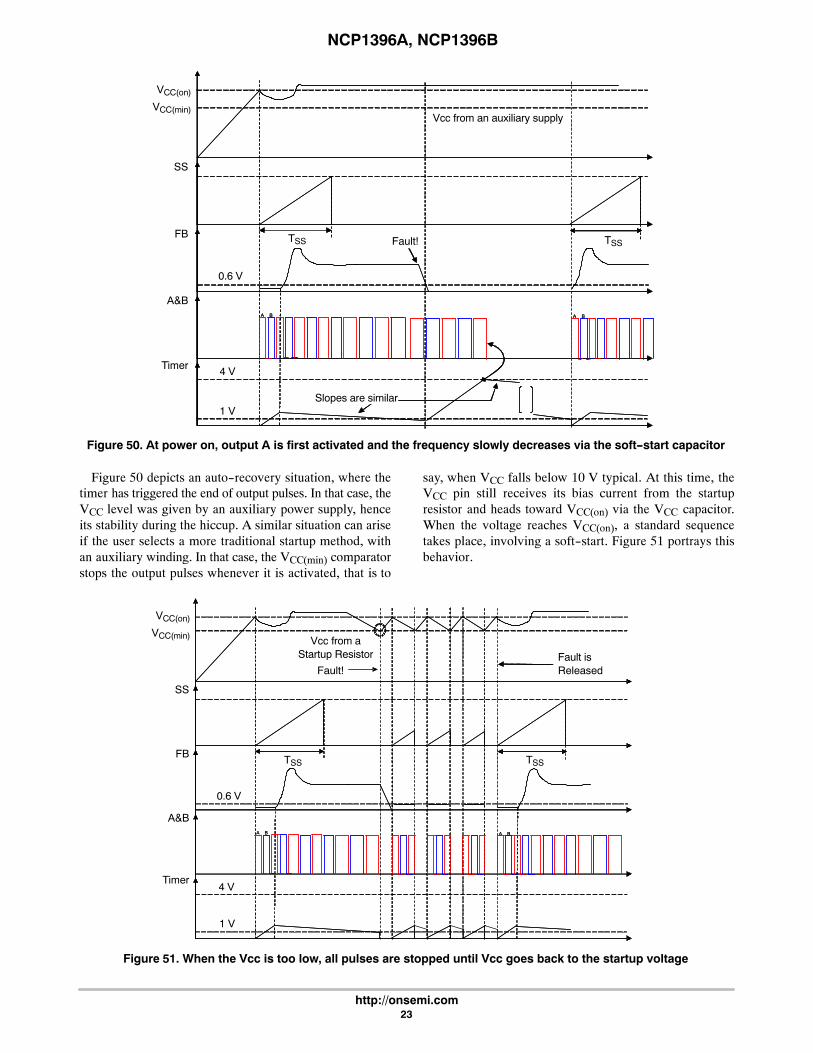
Startup BehaviourWhen the VCC voltage grows-up, the internal current
consumption is kept to Istrup, allowing to crank-up theconverter via a resistor connected to the bulk capacitor.When VCC reaches the VCC(on) level, output Mlower goeshigh first and then output Mupper. This sequence willalways be the same whatever triggers the pulse delivery:fault, OFF to ON etc… Pulsing the output Mlower high firstgives an immediate charge of the bootstrap capacitor.Then, the rest of pulses follow, delivered at the highestswitching value, set by the resistor on pin 2. The soft-startcapacitor ensures a smooth frequency decrease to either theprogrammed minimum value (in case of fault) or to a valuecorresponding to the operating point if the feedback loopcloses first. Figure 50 shows typical signals evolution atpower on.
NCP1396A, NCP1396B
http://onsemi.com23
Figure 50. At power on, output A is first activated and the frequency slowly decreases via the soft-start capacitor
A B
Fault!
0.6 V
Slopes are similar
A B
4 V
1 V
Vcc from an auxiliary supply
SS
FB
A B
A&B
Timer
A B
VCC(min)
VCC(on)
TSS TSS
Figure 50 depicts an auto-recovery situation, where thetimer has triggered the end of output pulses. In that case, theVCC level was given by an auxiliary power supply, henceits stability during the hiccup. A similar situation can ariseif the user selects a more traditional startup method, withan auxiliary winding. In that case, the VCC(min) comparatorstops the output pulses whenever it is activated, that is to
say, when VCC falls below 10�V typical. At this time, theVCC pin still receives its bias current from the startupresistor and heads toward VCC(on) via the VCC capacitor.When the voltage reaches VCC(on), a standard sequencetakes place, involving a soft-start. Figure 51 portrays thisbehavior.
Figure 51. When the Vcc is too low, all pulses are stopped until Vcc goes back to the startup voltage
SS
FB
A B
A&B
Timer
Fault!
0.6 V
A B
4 V
1 V
A B A B
VCC(min)
VCC(on)
Vcc from aStartup Resistor Fault is
Released
TSSTSS

NCP1396A, NCP1396B
http://onsemi.com24
As described in the data-sheet, two startup levelsVCC(on) are available, via two circuit versions. TheNCP1396 features sufficient hysteresis (3�V typically) toallow a classical startup method with a resistor connectedto the bulk capacitor. Then, at the end of the startupsequence, an auxiliary winding is supposed to take over thecontroller supply voltage. To the opposite, for applicationswhere the resonant controller is powered from a standbypower supply, the startup level is 10�V typically and allows
for the direct a connection from a 12�V source. Thanks tothis NCP1396B, simple ON/OFF operation is thereforefeasible.
The High-voltage DriverThe driver features a traditional bootstrap circuitry,
requiring an external high-voltage diode for the capacitorrefueling path. Figure 52 shows the internal architecture ofthe high-voltage section.
Figure 52. The Internal High-voltage Section of the NCP1396
+
Vboot
Mupper
HB
cboot
dboot
auxVcc
GND
Vcc
Mlower
HV
UVLO
S
Q
Q
R
Delay
LevelShifter
PulseTrigger
Fault
A
B
The device incorporates an upper UVLO circuitry thatmakes sure enough Vgs is available for the upper sideMOSFET. The B and A outputs are delivered by theinternal logic, as Figure 47 testifies. A delay is inserted inthe lower rail to ensure good matching between thesepropagating signals.
As stated in the maximum rating section, the floatingportion can go up to 600�VDC and makes the IC perfectlysuitable for offline applications featuring a 400�V PFCfront-end stage.
ORDERING INFORMATIONDevice Package Shipping†
NCP1396ADR2G SOIC-16, Less Pin 13(Pb-Free)
2500 / Tape & Reel
NCP1396BDR2G SOIC-16, Less Pin 13(Pb-Free)
2500 / Tape & Reel
NCP1396APG PDIP-16, Less Pin 13(Pb-Free)
25 Units / Rail
NCP1396BPG PDIP-16, Less Pin 13(Pb-Free)
25 Units / Rail
†For information on tape and reel specifications, including part orientation and tape sizes, please refer to our Tape and Reel Packaging SpecificationBrochure, BRD8011/D.
NCP1396A, NCP1396B
http://onsemi.com25
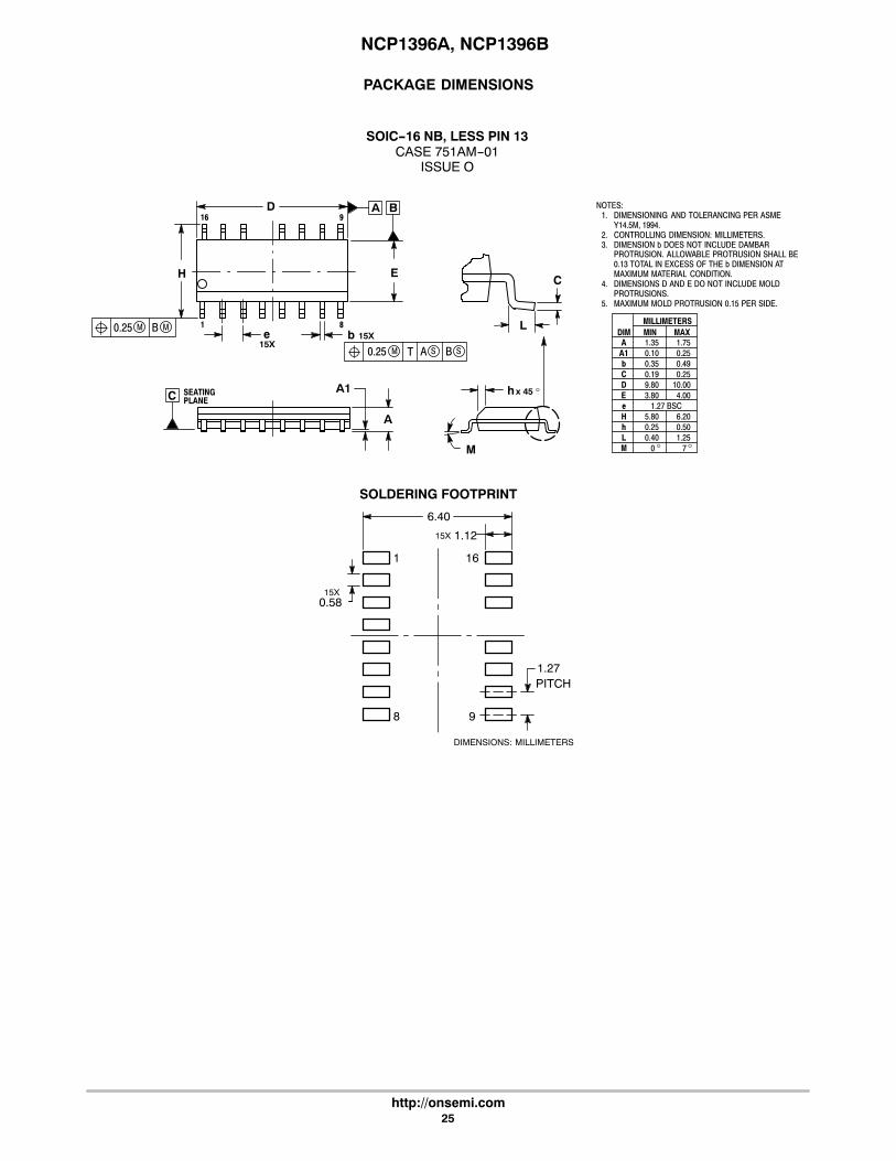
PACKAGE DIMENSIONS
SOIC-16 NB, LESS PIN 13CASE 751AM-01
ISSUE O
NOTES:1. DIMENSIONING AND TOLERANCING PER ASME
Y14.5M, 1994.2. CONTROLLING DIMENSION: MILLIMETERS.3. DIMENSION b DOES NOT INCLUDE DAMBAR
PROTRUSION. ALLOWABLE PROTRUSION SHALL BE0.13 TOTAL IN EXCESS OF THE b DIMENSION ATMAXIMUM MATERIAL CONDITION.
4. DIMENSIONS D AND E DO NOT INCLUDE MOLDPROTRUSIONS.
5. MAXIMUM MOLD PROTRUSION 0.15 PER SIDE.
1 8
16 9
SEATINGPLANE
L
M
hx 45�
e15X
H E
D
M0.25 B M
A1
A
DIM MIN MAXMILLIMETERS
D 9.80 10.00E 3.80 4.00
A 1.35 1.75
b 0.35 0.49
L 0.40 1.25
e 1.27 BSC
C 0.19 0.25
A1 0.10 0.25
M 0 7
H 5.80 6.20h 0.25 0.50
� �
6.40
15X0.58
15X 1.12
1.27
DIMENSIONS: MILLIMETERS
1
PITCH
SOLDERING FOOTPRINT
16
8 9
M0.25 A S
b 15X
T B S
A B
C
C
NCP1396A, NCP1396B
http://onsemi.com26
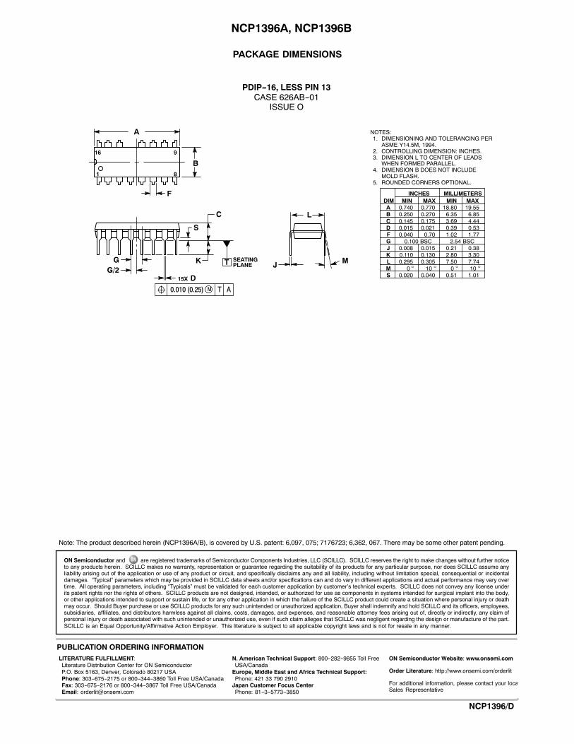
PACKAGE DIMENSIONS
PDIP-16, LESS PIN 13CASE 626AB-01
ISSUE O
NOTES:1. DIMENSIONING AND TOLERANCING PER
ASME Y14.5M, 1994.2. CONTROLLING DIMENSION: INCHES.3. DIMENSION L TO CENTER OF LEADS
WHEN FORMED PARALLEL.4. DIMENSION B DOES NOT INCLUDE
MOLD FLASH.5. ROUNDED CORNERS OPTIONAL.
B
F
C
S
G/2G
D
J
L
M
15X
SEATING
1 8
916
KPLANE
AM0.010 (0.25) T
DIM MIN MAX MIN MAXMILLIMETERSINCHES
A 0.740 0.770 18.80 19.55B 0.250 0.270 6.35 6.85C 0.145 0.175 3.69 4.44D 0.015 0.021 0.39 0.53F 0.040 0.70 1.02 1.77G 0.100 BSC 2.54 BSCJ 0.008 0.015 0.21 0.38K 0.110 0.130 2.80 3.30L 0.295 0.305 7.50 7.74M 0 10 0 10 S 0.020 0.040 0.51 1.01
����
A
T
ON Semiconductor and are registered trademarks of Semiconductor Components Industries, LLC (SCILLC). SCILLC reserves the right to make changes without further noticeto any products herein. SCILLC makes no warranty, representation or guarantee regarding the suitability of its products for any particular purpose, nor does SCILLC assume anyliability arising out of the application or use of any product or circuit, and specifically disclaims any and all liability, including without limitation special, consequential or incidentaldamages. “Typical” parameters which may be provided in SCILLC data sheets and/or specifications can and do vary in different applications and actual performance may vary overtime. All operating parameters, including “Typicals” must be validated for each customer application by customer's technical experts. SCILLC does not convey any license underits patent rights nor the rights of others. SCILLC products are not designed, intended, or authorized for use as components in systems intended for surgical implant into the body,or other applications intended to support or sustain life, or for any other application in which the failure of the SCILLC product could create a situation where personal injury or deathmay occur. Should Buyer purchase or use SCILLC products for any such unintended or unauthorized application, Buyer shall indemnify and hold SCILLC and its officers, employees,subsidiaries, affiliates, and distributors harmless against all claims, costs, damages, and expenses, and reasonable attorney fees arising out of, directly or indirectly, any claim ofpersonal injury or death associated with such unintended or unauthorized use, even if such claim alleges that SCILLC was negligent regarding the design or manufacture of the part.SCILLC is an Equal Opportunity/Affirmative Action Employer. This literature is subject to all applicable copyright laws and is not for resale in any manner.
PUBLICATION ORDERING INFORMATIONN. American Technical Support: 800-282-9855 Toll Free USA/CanadaEurope, Middle East and Africa Technical Support: Phone: 421 33 790 2910Japan Customer Focus Center Phone: 81-3-5773-3850
NCP1396/D
Note: The product described herein (NCP1396A/B), is covered by U.S. patent: 6,097, 075; 7176723; 6,362, 067. There may be some other patent pending.
LITERATURE FULFILLMENT: Literature Distribution Center for ON Semiconductor P.O. Box 5163, Denver, Colorado 80217 USA Phone: 303-675-2175 or 800-344-3860 Toll Free USA/Canada Fax: 303-675-2176 or 800-344-3867 Toll Free USA/Canada Email: [email protected]
ON Semiconductor Website: www.onsemi.com
Order Literature: http://www.onsemi.com/orderlit
For additional information, please contact your locaSales Representative