Embed Size (px)
Citation preview
© Semiconductor Components Industries, LLC, 2009
September, 2009 − Rev. 61 Publication Order Number:
NCP1271/D
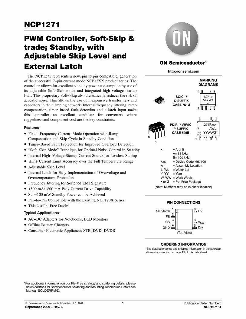
NCP1271
PWM Controller, Soft-Skip & trade; Standby, with Adjustable Skip Level and External Latch
The NCP1271 represents a new, pin to pin compatible, generation of the successful 7−pin current mode NCP12XX product series. The controller allows for excellent stand by power consumption by use of its adjustable Soft−Skip mode and integrated high voltage startup FET. This proprietary Soft−Skip also dramatically reduces the risk of acoustic noise. This allows the use of inexpensive transformers and capacitors in the clamping network. Internal frequency jittering, ramp compensation, timer−based fault detection and a latch input make this controller an excellent candidate for converters where ruggedness and component cost are the key constraints.
Features
• Fixed−Frequency Current−Mode Operation with RampCompensation and Skip Cycle in Standby Condition
• Timer−Based Fault Protection for Improved Overload Detection• “Soft−Skip Mode” Technique for Optimal Noise Control in Standby
• Internal High−Voltage Startup Current Source for Lossless Startup
• �5% Current Limit Accuracy over the Full Temperature Range
• Adjustable Skip Level• Internal Latch for Easy Implementation of Overvoltage and
Overtemperature Protection• Frequency Jittering for Softened EMI Signature
• +500 mA/−800 mA Peak Current Drive Capability
• Sub−100 mW Standby Power can be Achieved• Pin−to−Pin Compatible with the Existing NCP120X Series
• This is a Pb−Free Device
Typical Applications
• AC−DC Adapters for Notebooks, LCD Monitors
• Offline Battery Chargers
• Consumer Electronic Appliances STB, DVD, DVDR
*For additional information on our Pb−Free strategy and soldering details, pleasedownload the ON Semiconductor Soldering and Mounting Techniques ReferenceManual, SOLDERRM/D.
PIN CONNECTIONS
http://onsemi.com
MARKINGDIAGRAMS
(Top View)
1271xALYW�
�
x = A or BA= 65 kHzB= 100 kHz
xxx = Device Code: 65, 100A = Assembly LocationL, WL = Wafer LotY, YY = YearW, WW = Work Week� or G = Pb−Free Package
1
8
(Note: Microdot may be in either location)
Skip/latch
FB
CS
GND
1
2
3
4
HV
VCC
Drv
8
6
5
SOIC−7D SUFFIX
CASE 751U
See detailed ordering and shipping information in the packagedimensions section on page 19 of this data sheet.
ORDERING INFORMATION
PDIP−7 VHVICP SUFFIX
CASE 626B
1
8
1271PxxxAWL
YYWWG
1
NCP1271
http://onsemi.com2
Figure 1. Typical Application Circuit
skip/latchFBCSGnd
NCP1271
Voltage
+
−
ACInput
Output
Rramp
latch input*
EMI
Filter
Rskip
HV
VccDrv
**Optional
NCP1271
http://onsemi.com3
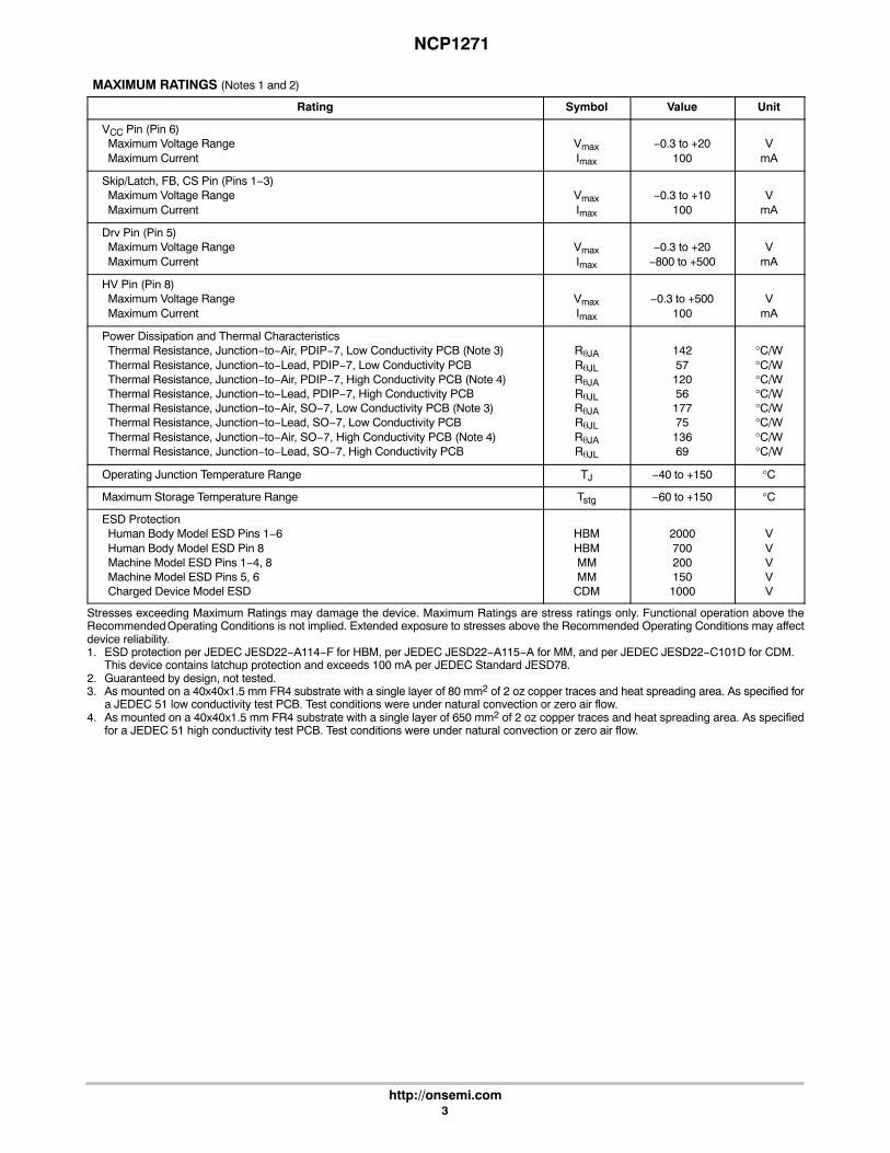
MAXIMUM RATINGS (Notes 1 and 2)
Rating Symbol Value Unit
VCC Pin (Pin 6)Maximum Voltage RangeMaximum Current
VmaxImax
−0.3 to +20100
VmA
Skip/Latch, FB, CS Pin (Pins 1−3)Maximum Voltage RangeMaximum Current
VmaxImax
−0.3 to +10100
VmA
Drv Pin (Pin 5)Maximum Voltage RangeMaximum Current
VmaxImax
−0.3 to +20−800 to +500
VmA
HV Pin (Pin 8)Maximum Voltage RangeMaximum Current
VmaxImax
−0.3 to +500100
VmA
Power Dissipation and Thermal CharacteristicsThermal Resistance, Junction−to−Air, PDIP−7, Low Conductivity PCB (Note 3)Thermal Resistance, Junction−to−Lead, PDIP−7, Low Conductivity PCBThermal Resistance, Junction−to−Air, PDIP−7, High Conductivity PCB (Note 4)Thermal Resistance, Junction−to−Lead, PDIP−7, High Conductivity PCBThermal Resistance, Junction−to−Air, SO−7, Low Conductivity PCB (Note 3)Thermal Resistance, Junction−to−Lead, SO−7, Low Conductivity PCBThermal Resistance, Junction−to−Air, SO−7, High Conductivity PCB (Note 4)Thermal Resistance, Junction−to−Lead, SO−7, High Conductivity PCB
R�JAR�JLR�JAR�JLR�JAR�JLR�JAR�JL
14257120561777513669
°C/W°C/W°C/W°C/W°C/W°C/W°C/W°C/W
Operating Junction Temperature Range TJ −40 to +150 °C
Maximum Storage Temperature Range Tstg −60 to +150 °C
ESD ProtectionHuman Body Model ESD Pins 1−6Human Body Model ESD Pin 8Machine Model ESD Pins 1−4, 8Machine Model ESD Pins 5, 6Charged Device Model ESD
HBMHBMMMMM
CDM
20007002001501000
VVVVV
Stresses exceeding Maximum Ratings may damage the device. Maximum Ratings are stress ratings only. Functional operation above theRecommended Operating Conditions is not implied. Extended exposure to stresses above the Recommended Operating Conditions may affectdevice reliability.1. ESD protection per JEDEC JESD22−A114−F for HBM, per JEDEC JESD22−A115−A for MM, and per JEDEC JESD22−C101D for CDM.
This device contains latchup protection and exceeds 100 mA per JEDEC Standard JESD78.2. Guaranteed by design, not tested.3. As mounted on a 40x40x1.5 mm FR4 substrate with a single layer of 80 mm2 of 2 oz copper traces and heat spreading area. As specified for
a JEDEC 51 low conductivity test PCB. Test conditions were under natural convection or zero air flow.4. As mounted on a 40x40x1.5 mm FR4 substrate with a single layer of 650 mm2 of 2 oz copper traces and heat spreading area. As specified
for a JEDEC 51 high conductivity test PCB. Test conditions were under natural convection or zero air flow.
NCP1271
http://onsemi.com4
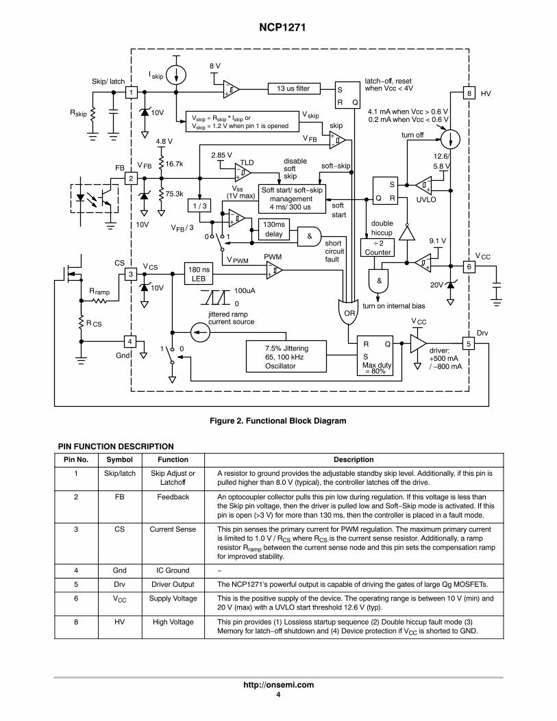
Figure 2. Functional Block Diagram
−
LEB
Skip/ latch
CS
FB
7.5% Jittering65, 100 kHzOscillator
130msdelay
HVS
R
Drv
Gnd
PWM
skip
OR
4.8 V
8 V
Max duty
R
S
= 80%
180 ns
0 &
+
−+
−+
−+
soft−skip
8
2
3
4
1
6
5
Vss
V FB
latch−off, resetwhen Vcc < 4V
jittered rampcurrent source
I
V
shortcircuitfault
12.6/5.8 V
9.1 V
turn off
UVLO
−+
−+
turn on internal bias
4.1 mA when Vcc > 0.6 V
driver:+500 mA/ −800 mA
10V
disablesoftskip
skip
&
doublehiccup
S
Q
10V
10V 20V
V CS
V CC
V CC
0
100uA
0.2 mA when Vcc < 0.6 V
Soft start/ soft−skipmanagement
−TLD
+
softstart
2.85 V
1 / 3
13 us filter
1 0
skip
Rskip
4 ms/ 300 us
R CS
Rramp
(1V max)
16.7k
75.3k
V / 3FB
V PWM
V FB
Q
R
Q
�2Counter
Vskip = Rskip * Iskip or Vskip = 1.2 V when pin 1 is opened
1
PIN FUNCTION DESCRIPTION
Pin No. Symbol Function Description
1 Skip/latch Skip Adjust orLatchoff
A resistor to ground provides the adjustable standby skip level. Additionally, if this pin ispulled higher than 8.0 V (typical), the controller latches off the drive.
2 FB Feedback An optocoupler collector pulls this pin low during regulation. If this voltage is less thanthe Skip pin voltage, then the driver is pulled low and Soft−Skip mode is activated. If thispin is open (>3 V) for more than 130 ms, then the controller is placed in a fault mode.
3 CS Current Sense This pin senses the primary current for PWM regulation. The maximum primary currentis limited to 1.0 V / RCS where RCS is the current sense resistor. Additionally, a rampresistor Rramp between the current sense node and this pin sets the compensation rampfor improved stability.
4 Gnd IC Ground −
5 Drv Driver Output The NCP1271’s powerful output is capable of driving the gates of large Qg MOSFETs.
6 VCC Supply Voltage This is the positive supply of the device. The operating range is between 10 V (min) and20 V (max) with a UVLO start threshold 12.6 V (typ).
8 HV High Voltage This pin provides (1) Lossless startup sequence (2) Double hiccup fault mode (3)Memory for latch−off shutdown and (4) Device protection if VCC is shorted to GND.
NCP1271
http://onsemi.com5
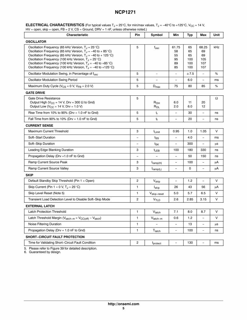
ELECTRICAL CHARACTERISTICS (For typical values TJ = 25°C, for min/max values, TJ = −40°C to +125°C, VCC = 14 V, HV = open, skip = open, FB = 2 V, CS = Ground, DRV = 1 nF, unless otherwise noted.)
Characteristic Pin Symbol Min Typ Max Unit
OSCILLATOR
Oscillation Frequency (65 kHz Version, TJ = 25�C)Oscillation Frequency (65 kHz Version, TJ = −40 to + 85�C)Oscillation Frequency (65 kHz Version, TJ = −40 to + 125�C)Oscillation Frequency (100 kHz Version, TJ = 25�C)Oscillation Frequency (100 kHz Version, TJ = −40 to +85�C)Oscillation Frequency (100 kHz Version, TJ = −40 to +125�C)
5 fosc 61.755855958985
656565100100100
68.256969105107107
kHz
Oscillator Modulation Swing, in Percentage of fosc 5 − − �7.5 − %
Oscillator Modulation Swing Period 5 − − 6.0 − ms
Maximum Duty Cycle (VCS = 0 V, VFB = 2.0 V) 5 Dmax 75 80 85 %
GATE DRIVE
Gate Drive ResistanceOutput High (VCC = 14 V, Drv = 300 � to Gnd)Output Low (VCC = 14 V, Drv = 1.0 V)
5ROHROL
6.02.0
116.0
2012
�
Rise Time from 10% to 90% (Drv = 1.0 nF to Gnd) 5 tr − 30 − ns
Fall Time from 90% to 10% (Drv = 1.0 nF to Gnd) 5 tf − 20 − ns
CURRENT SENSE
Maximum Current Threshold 3 ILimit 0.95 1.0 1.05 V
Soft−Start Duration − tSS − 4.0 − ms
Soft−Skip Duration − tSK − 300 − �s
Leading Edge Blanking Duration 3 tLEB 100 180 330 ns
Propagation Delay (Drv =1.0 nF to Gnd) − − − 50 150 ns
Ramp Current Source Peak 3 Iramp(H) − 100 − �A
Ramp Current Source Valley 3 Iramp(L) − 0 − �A
SKIP
Default Standby Skip Threshold (Pin 1 = Open) 2 Vskip − 1.2 − V
Skip Current (Pin 1 = 0 V, TJ = 25�C) 1 Iskip 26 43 56 �A
Skip Level Reset (Note 5) 1 Vskip−reset 5.0 5.7 6.5 V
Transient Load Detection Level to Disable Soft−Skip Mode 2 VTLD 2.6 2.85 3.15 V
EXTERNAL LATCH
Latch Protection Threshold 1 Vlatch 7.1 8.0 8.7 V
Latch Threshold Margin (Vlatch−m = VCC(off) − Vlatch) 1 Vlatch−m 0.6 1.2 − V
Noise Filtering Duration 1 − − 13 − �s
Propagation Delay (Drv = 1.0 nF to Gnd) 1 Tlatch − 100 − ns
SHORT−CIRCUIT FAULT PROTECTION
Time for Validating Short−Circuit Fault Condition 2 tprotect − 130 − ms
5. Please refer to Figure 39 for detailed description.6. Guaranteed by design.
NCP1271
http://onsemi.com6
ELECTRICAL CHARACTERISTICS (continued) (For typical values TJ = 25°C, for min/max values, TJ = −40°C to +125°C,VCC = 14 V, HV = open, skip = open, FB = 2 V, CS = Ground, DRV = 1 nF, unless otherwise noted.)
Characteristic Pin Symbol Min Typ Max Unit
STARTUP CURRENT SOURCE
High−Voltage Current SourceInhibit Voltage (ICC = 200 �A, HV = 50 V)Inhibit Current (VCC = 0 V, HV = 50 V)Startup (VCC = VCC(on) − 0.2 V, HV = 50 V)Leakage (VCC = 14 V, HV = 500 V)
6668
VinhibitIinhibitIHV
IHV−leak
190803.010
6002004.125
8003506.050
mV�AmA�A
Minimum Startup Voltage (VCC = VCC(on) – 0.2 V, ICC = 0.5 mA) 8 VHV(min) − 20 28 V
SUPPLY SECTION
VCC RegulationStartup Threshold, VCC IncreasingMinimum Operating Voltage After Turn−OnVCC Operating HysteresisUndervoltage Lockout Threshold Voltage, VCC DecreasingLogic Reset Level (VCC(latch) –VCC(reset) > 1.0 V) (Note 7)
6VCC(on)VCC(off)
VCC(on) − VCC(off)VCC(latch)VCC(reset)
11.28.23.05.0−
12.69.13.65.84.0
13.8104.26.5−
VVVVV
VCC Supply CurrentOperating (VCC = 14 V, 1.0 nF Load, VFB = 2.0 V, 65 kHz Version)Operating (VCC = 14 V, 1.0 nF Load, VFB = 2.0 V, 100 kHz Version)Output Stays Low (VCC = 14 V, VFB = 0 V)Latchoff Phase (VCC = 7.0 V, VFB = 2.0 V)
6ICC1ICC1ICC2ICC3
−−−−
2.33.11.3500
3.03.52.0720
mAmAmA�A
7. Guaranteed by design.
TYPICAL CHARACTERISTICS
Figure 3. Oscillation Frequency vs.Temperature
Figure 4. Maximum Duty Cycle vs.Temperature
TEMPERATURE (°C) TEMPERATURE (°C)
1251007550250−5050
60
70
80
90
100
110
1251007550250−5075
76
77
78
79
80
81
OS
CIL
LAT
ION
FR
EQ
UE
NC
Y (
kHz)
MA
XIM
UM
DU
TY
CY
CLE
(%
)
−25 −25
82
83
84
85
100 kHz
65 kHz
NCP1271
http://onsemi.com7
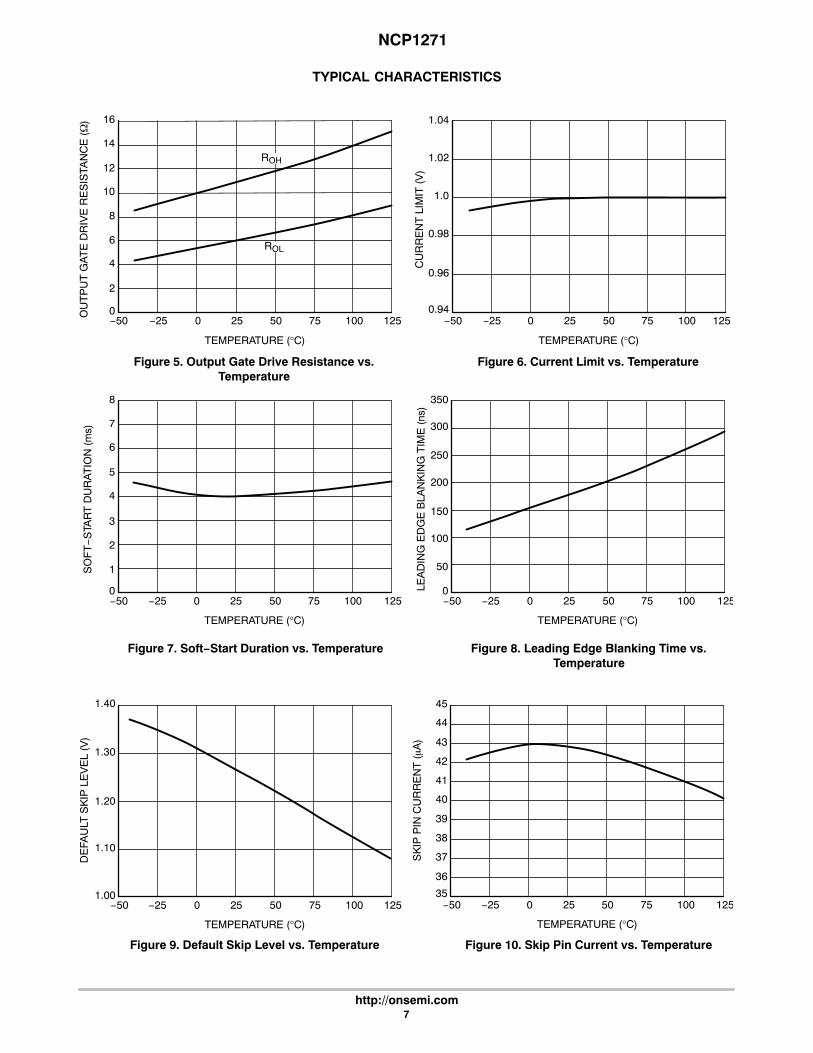
TYPICAL CHARACTERISTICS
Figure 5. Output Gate Drive Resistance vs.Temperature
Figure 6. Current Limit vs. Temperature
Figure 7. Soft−Start Duration vs. Temperature Figure 8. Leading Edge Blanking Time vs.Temperature
TEMPERATURE (°C) TEMPERATURE (°C)
1251007550250−500
2
4
6
8
10
1251007550250−500.94
0.96
0.98
1.0
1.04
OU
TP
UT
GA
TE
DR
IVE
RE
SIS
TAN
CE
(�
)
CU
RR
EN
T L
IMIT
(V
)
Figure 9. Default Skip Level vs. Temperature Figure 10. Skip Pin Current vs. Temperature
TEMPERATURE (°C)
1251007550250−500
100
200
300LE
AD
ING
ED
GE
BLA
NK
ING
TIM
E (
ns)
TEMPERATURE (°C)
1251007550250−501.00
1.10
1.20
1.30
1.40
DE
FAU
LT S
KIP
LE
VE
L (V
)
50
150
250
350
−25 −25
−25
−25
12
14
16
ROH
ROL
1.02
TEMPERATURE (°C)
1251007550250−500
2
4
6
SO
FT−
STA
RT
DU
RA
TIO
N (
ms)
1
3
5
8
−25
7
TEMPERATURE (°C)
1251007550250−5035
36
37
38
39
40
41
SK
IP P
IN C
UR
RE
NT
(�A
)
−25
42
43
44
45
NCP1271
http://onsemi.com8
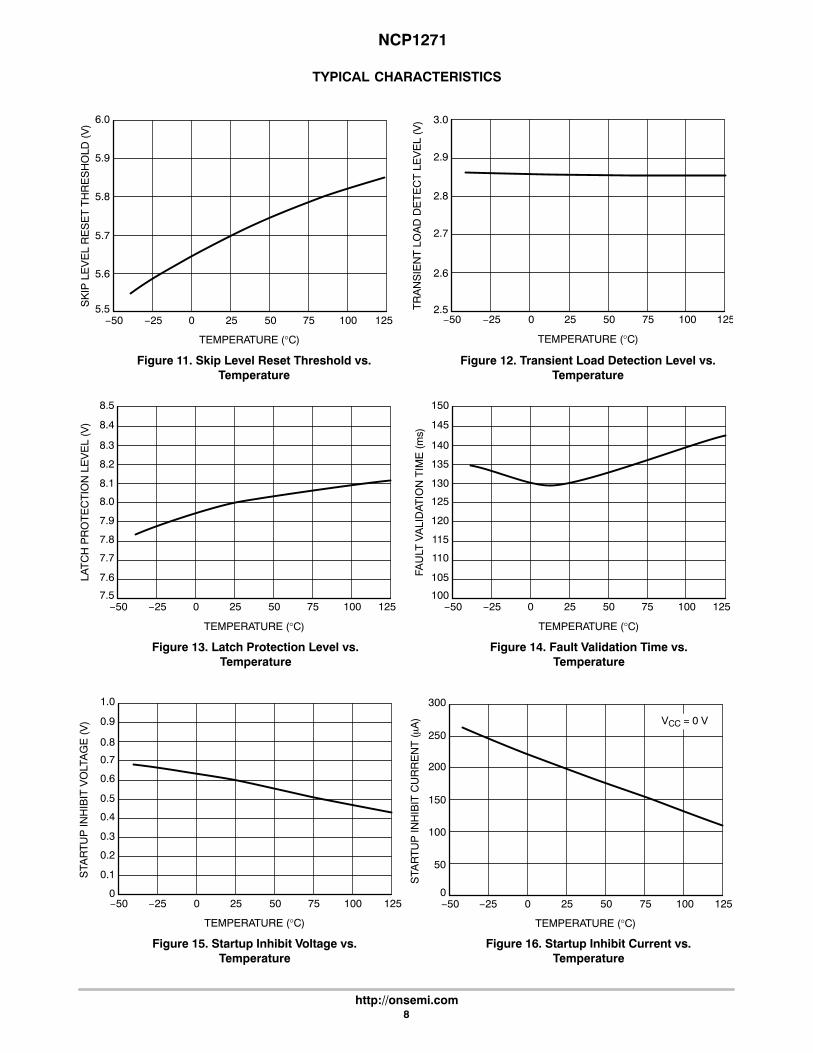
TYPICAL CHARACTERISTICS
Figure 11. Skip Level Reset Threshold vs.Temperature
Figure 12. Transient Load Detection Level vs.Temperature
TEMPERATURE (°C)
1251007550250−505.5
5.6
5.7
5.8
5.9
6.0
SK
IP L
EV
EL
RE
SE
T T
HR
ES
HO
LD (
V)
Figure 13. Latch Protection Level vs.Temperature
Figure 14. Fault Validation Time vs.Temperature
TEMPERATURE (°C)
TEMPERATURE (°C)
1251007550250−502.5
2.6
2.7
2.8
2.9
3.0
1251007550250−507.5
7.6
7.7
7.8
7.9
TR
AN
SIE
NT
LO
AD
DE
TE
CT
LE
VE
L (V
)
LAT
CH
PR
OT
EC
TIO
N L
EV
EL
(V)
Figure 15. Startup Inhibit Voltage vs.Temperature
Figure 16. Startup Inhibit Current vs.Temperature
TEMPERATURE (°C)
1251007550250−500
0.2
0.4
0.6
0.8
1.0
STA
RT
UP
INH
IBIT
VO
LTA
GE
(V
)
TEMPERATURE (°C)
1251007550250−500
50
100
150
200
250
STA
RT
UP
INH
IBIT
CU
RR
EN
T (�A
)
300
0.1
0.3
0.5
0.7
0.9
−25 −25
−25
−25 −25
8.0
8.1
8.2
8.3
8.4
8.5
VCC = 0 V
TEMPERATURE (°C)
1251007550250−50100
105
110
115
120
FAU
LT V
ALI
DAT
ION
TIM
E (
ms)
−25
125
130
135
140
145
150
NCP1271
http://onsemi.com9
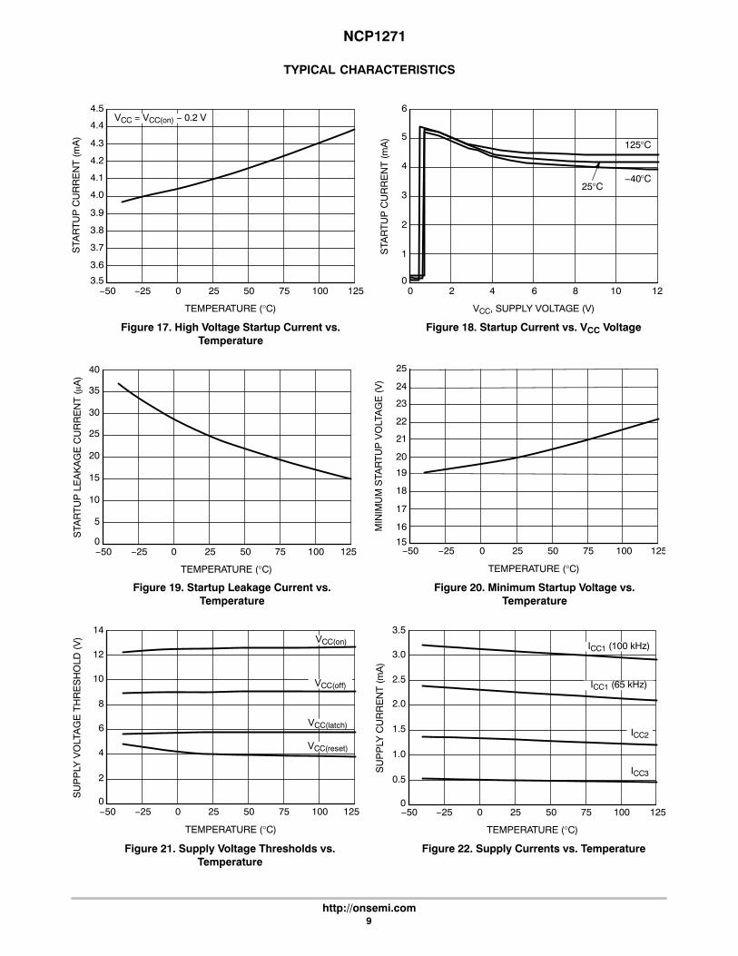
TYPICAL CHARACTERISTICS
Figure 17. High Voltage Startup Current vs.Temperature
Figure 18. Startup Current vs. VCC Voltage
TEMPERATURE (°C) VCC, SUPPLY VOLTAGE (V)
1251007550250−503.5
3.6
3.7
3.8
3.9
4.0
4.1
121086400
1
2
3
4
5
6
STA
RT
UP
CU
RR
EN
T (
mA
)
STA
RT
UP
CU
RR
EN
T (
mA
)
Figure 19. Startup Leakage Current vs.Temperature
Figure 20. Minimum Startup Voltage vs.Temperature
TEMPERATURE (°C)
TEMPERATURE (°C)
1251007550250−5015
17
19
21
23
25
1251007550250−500
2
4
6
8
MIN
IMU
M S
TAR
TU
P V
OLT
AG
E (
V)
SU
PP
LY V
OLT
AG
E T
HR
ES
HO
LD (
V)
Figure 21. Supply Voltage Thresholds vs.Temperature
TEMPERATURE (°C)
1251007550250−500
0.5
1.0
1.5
2.0
2.5
SU
PP
LY C
UR
RE
NT
(m
A)
−25 2
−25
−25 −25
VCC(reset)
VCC(on)
4.2
4.3
4.4
4.5
16
18
20
22
24
10
12
14
VCC(off)
VCC(latch)
VCC = VCC(on) − 0.2 V
3.0
3.5
Figure 22. Supply Currents vs. Temperature
TEMPERATURE (°C)
1251007550250−500
5
10
15
20
25
30
STA
RT
UP
LE
AK
AG
E C
UR
RE
NT
(�A
)
−25
35
40
125°C
−40°C25°C
ICC1 (100 kHz)
ICC2
ICC3
ICC1 (65 kHz)
NCP1271
http://onsemi.com10
OPERATING DESCRIPTION
IntroductionThe NCP1271 represents a new generation of the
fixed−frequency PWM current−mode flyback controllersfrom ON Semiconductor. The device features integratedhigh−voltage startup and excellent standby performance.The proprietary Soft−Skip Mode achieves extremelylow−standby power consumption while keeping powersupply acoustic noise to a minimum. The key features ofthe NCP1271 are as follows:• Timer−Based Fault Detection: In the event that an
abnormally large load is applied to the output for morethan 130 ms, the controller will safely shut theapplication down. This allows accurate overload (OL)or short−circuit (SC) detection which is not dependenton the auxiliary winding.
• Soft−Skip Mode: This proprietary feature of theNCP1271 minimizes the standby low−frequencyacoustic noise by ramping the peak current envelopewhenever skip is activated.
• Adjustable Skip Threshold: This feature allows thepower level at which the application enters skip to befully adjusted. Thus, the standby power for variousapplications can be optimized. The default skip levelis 1.2 V (40% of the maximum peak current).
• 500 V High−Voltage Startup Capability: ThisAC−DC application friendly feature eliminates theneed for an external startup biasing circuit, minimizesthe standby power loss, and saves printed circuit board(PCB) space.
• Dual High−Voltage Startup−Current Levels: TheNCP1271 uniquely provides the ability to reduce thestartup current supply when Vcc is low. This preventsdamage if Vcc is ever shorted to ground. After Vccrises above approximately 600 mV, the startup currentincreases to its full value and rapidly charges the Vcccapacitor.
• Latched Protection: The NCP1271 provides a pin,which if pulled high, places the part in a latched offmode. Therefore, overvoltage (OVP) andovertemperature (OTP) protection can be easilyimplemented. A noise filter is provided on this functionto reduce the chances of falsely triggering the latch. Thelatch is released when Vcc is cycled below 4 V.
• Non−Latched Protection/ Shutdown Option: Bypulling the feedback pin below the skip thresholdlevel, a non−latching shutdown mode can be easilyimplemented.
• 4.0 ms Soft−Start: The soft start feature slowly rampsup the drive duty cycle at startup. This forces theprimary current to also ramp up slowly anddramatically reduces the stress on power componentsduring startup.
• Current−Mode Operation: The NCP1271 usescurrent−mode control which provides better transientresponse than voltage−mode control. Current−modecontrol also inherently limits the cycle−by−cycleprimary current.
• Compensation Ramp: A drawback of current−moderegulation is that the circuit may become unstablewhen the operating duty cycle is too high. TheNCP1271 offers an adjustable compensation ramp tosolve this instability.
• 80% Maximum Duty Cycle Protection: This featurelimits the maximum on time of the drive to protect thepower MOSFET from being continuously on.
• Frequency Jittering: Frequency jittering softens theEMI signature by spreading out peak energy within aband +/− 7.5% from the center frequency.
• Switching Frequency Options: The NCP1271 isavailable in either 65 kHz or 100 kHz fixed frequencyoptions. Depending on the application, the designercan pick the right device to help reduce magneticswitching loss or improve the EMI signature beforereaching the 150 kHz starting point for morerestrictive EMI test limits.
NCP1271 Operating ConditionsThere are 5 possible operating conditions for the NCP1271:
1. Normal Operation – When VCC is above VCC(off)(9.1 V typical) and the feedback pin voltage (VFB)is within the normal operation range (i.e.,VFB < 3.0V), the NCP1271 operates as a fixed−frequencycurrent−mode PWM controller.
2. Standby Operation (or Skip−Cycle Operation)When the load current drops, the compensationnetwork responds by reducing the primary peakcurrent. When the peak current reaches the skippeak current level, the NCP1271 enters Soft−Skipoperation to reduce the power consumption. ThisSoft−Skip feature offers a modified peak currentenvelope and hence also reduces the risk of audiblenoise. In the event of a sudden load increase, thetransient load detector (TLD) disables Soft−Skipand applies maximum power to bring the outputinto regulation as fast as possible.
3. Fault Operation – When no feedback signal isreceived for 130 ms or when VCC drops belowVCC(off) (9.1 V typical), the NCP1271 recognizes itas a fault condition. In this fault mode, the Vccvoltage is forced to go through two cycles of slowlydischarging and charging. This is known as a“double hiccup.” The double hiccup insures thatample time is allowed between restarts to preventoverheating of the power devices. If the fault is
NCP1271
http://onsemi.com11
cleared after the double hiccup, then the applicationrestarts. If not, then the process is repeated.
4. Latched Shutdown – When the Skip/latch pin (Pin1) voltage is pulled above 8.0 V for more than13 �s, the NCP1271 goes into latchoff shutdown.The output is held low and VCC stays in hiccupmode until the latch is reset. The reset can onlyoccur if Vcc is allowed to fall below VCC(reset)(4.0 V typical). This is generally accomplished byunplugging the main input AC source.
5. Non−Latched Shutdown – If the FB pin is pulledbelow the skip level, then the device will enter anon−latched shutdown mode. This mode disablesthe driver, but the controller automatically recoverswhen the pulldown on FB is released. Alternatively,Vcc can also be pulled low (below 190 mV) toshutdown the controller. This has the added benefitof placing the part into a low current consumptionmode for improved power savings.
Biasing the ControllerDuring startup, the Vcc bias voltage is supplied by the
HV Pin (Pin 8). This pin is capable of supporting up to500 V, so it can be connected directly to the bulk capacitor.Internally, the pin connects to a current source whichrapidly charges VCC to its VCC(on) threshold. After thislevel is reached, the controller turns on and the transformerauxiliary winding delivers the bias supply voltage to VCC.The startup FET is then turned off, allowing the standbypower loss to be minimized. This in−chip startup circuitminimizes the number of external components and PrintedCircuit Board (PCB) area. It also provides much lowerpower dissipation and faster startup times when comparedto using startup resistors to VCC. The auxiliary windingneeds to be designed to supply a voltage above the VCC(off)level but below the maximum VCC level of 20 V.
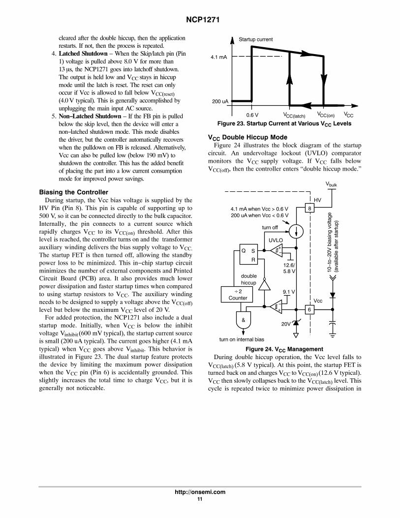
For added protection, the NCP1271 also include a dualstartup mode. Initially, when VCC is below the inhibitvoltage Vinhibit (600 mV typical), the startup current sourceis small (200 uA typical). The current goes higher (4.1 mAtypical) when VCC goes above Vinhibit. This behavior isillustrated in Figure 23. The dual startup feature protectsthe device by limiting the maximum power dissipationwhen the VCC pin (Pin 6) is accidentally grounded. Thisslightly increases the total time to charge VCC, but it isgenerally not noticeable.
Figure 23. Startup Current at Various VCC Levels
VVCC(on) CC
4.1 mA
200 uA
Startup current
0.6 V VCC(latch)
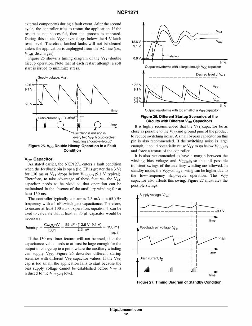
VCC Double Hiccup ModeFigure 24 illustrates the block diagram of the startup
circuit. An undervoltage lockout (UVLO) comparatormonitors the VCC supply voltage. If VCC falls belowVCC(off), then the controller enters “double hiccup mode.”
Figure 24. VCC Management
Vcc
HV
8
6
12.6/5.8 V
9.1 V
turn off
UVLO
−+
−+
turn on internal bias
&
doublehiccup
Q
R
20V
4.1 mA when Vcc > 0.6 V200 uA when Vcc < 0.6 V
10−t
o−20
V b
iasi
ng v
olta
ge(a
vaila
ble
afte
r st
artu
p)
�2Counter
S
Vbulk
During double hiccup operation, the Vcc level falls toVCC(latch) (5.8 V typical). At this point, the startup FET isturned back on and charges VCC to VCC(on) (12.6 V typical).VCC then slowly collapses back to the VCC(latch) level. Thiscycle is repeated twice to minimize power dissipation in
NCP1271
http://onsemi.com12
external components during a fault event. After the secondcycle, the controller tries to restart the application. If therestart is not successful, then the process is repeated.During this mode, VCC never drops below the 4 V latchreset level. Therefore, latched faults will not be clearedunless the application is unplugged from the AC line (i.e.,Vbulk discharges).
Figure 25 shows a timing diagram of the VCC doublehiccup operation. Note that at each restart attempt, a softstart is issued to minimize stress.
Figure 25. VCC Double Hiccup Operation in a FaultCondition
5.8 V
12.6 V9.1 V
Dtstartup
time
CCSupply voltage, V
time
Drain current, I
Switching is missing in every two VCC hiccup cyclesfeaturing a “double−hiccup”
VCC CapacitorAs stated earlier, the NCP1271 enters a fault condition
when the feedback pin is open (i.e. FB is greater than 3 V)for 130 ms or VCC drops below VCC(off) (9.1 V typical).Therefore, to take advantage of these features, the VCCcapacitor needs to be sized so that operation can bemaintained in the absence of the auxiliary winding for atleast 130 ms.
The controller typically consumes 2.3 mA at a 65 kHzfrequency with a 1 nF switch gate capacitance. Therefore,to ensure at least 130 ms of operation, equation 1 can beused to calculate that at least an 85 �F capacitor would benecessary.
tstartup �CVCC�V
ICC1�
85 �F · (12.6 V−9.1 V)2.3 mA
� 130 ms
(eq. 1)
If the 130 ms timer feature will not be used, then thecapacitance value needs to at least be large enough for theoutput to charge up to a point where the auxiliary windingcan supply VCC. Figure 26 describes different startupscenarios with different VCC capacitor values. If the VCCcap is too small, the application fails to start because thebias supply voltage cannot be established before VCC isreduced to the VCC(off) level.
Figure 26. Different Startup Scenarios of theCircuits with Different VCC Capacitors
time
V
Vout
CC
time
VCC
outV
9.1 V12.6 V
5.8 V
9.1 V12.6 V
tstartup0.6 V
0.6 V
Output waveforms with a large enough VCC capacitor
Output waveforms with too small of a VCC capacitor
Desired level of Vout
It is highly recommended that the VCC capacitor be asclose as possible to the VCC and ground pins of the productto reduce switching noise. A small bypass capacitor on thispin is also recommended. If the switching noise is largeenough, it could potentially cause VCC to go below VCC(off)and force a restart of the controller.
It is also recommended to have a margin between thewinding bias voltage and VCC(off) so that all possibletransient swings of the auxiliary winding are allowed. Instandby mode, the VCC voltage swing can be higher due tothe low−frequency skip−cycle operation. The VCCcapacitor also affects this swing. Figure 27 illustrates thepossible swings.
Figure 27. Timing Diagram of Standby Condition
V
FB
D
9.1 V
CC
skip
time
Supply voltage, V
time
Feedback pin voltage, V
time
Drain current, I
NCP1271
http://onsemi.com13
Soft−Start OperationFigures 28 and 29 show how the soft−start feature is
included in the pulse−width modulation (PWM)comparator. When the NCP1271 starts up, a soft−startvoltage VSS begins at 0 V. VSS increases gradually from 0 Vto 1.0 V in 4.0 ms and stays at 1.0 V afterward. This voltageVSS is compared with the divided−by−3 feedback pinvoltage (VFB/3). The lesser of VSS and (VFB/3) becomes themodulation voltage VPWM in the PWM duty cyclegeneration. Initially, (VFB/3) is above 1.0 V because theoutput voltage is low. As a result, VPWM is limited by thesoft start function and slowly ramps up the duty cycle (andtherefore the primary current) for the initial 4.0 ms. Thisprovides a greatly reduced stress on the power devicesduring startup.
Figure 28. VPWM is the lesser of VSS and (VFB/3)
0 1
−+
VSS
V / 3FB
VPWM
Figure 29. Soft−Start (Time = 0 at VCC = VCC(on))
time
time
time
1 V
4 ms
1 V
1 V
4 ms
time must be less than130 msto prevent fault condition
time4 ms
Feedback pin voltage divided−by−3, VFB/3
Pulse Width Modulation voltage, VPWM
Drain Current, ID
Soft−start voltage, VSS
Current−Mode Pulse−Width ModulationThe NCP1271 uses a current−mode fixed−frequency
PWM with internal ramp compensation. A pair of currentsense resistors RCS and Rramp sense the flyback draincurrent ID. As the drain current ramps up through theinductor and current sense resistor, a corresponding voltageramp is placed on the CS pin (pin 3). This voltage rangesfrom very low to as high as the modulation voltage VPWM(maximum of 1.0 V) before turning the drive off. If theinternal current ramp is ignored (i.e., Rramp ≈ 0) then themaximum possible drain current ID(max) is shown inEquation 2. This sets the primary current limit on a cycleby cycle basis.
ID(max) �1 V
RCS(eq. 2)
Figure 30. Current−Mode Implementation
LEBCS
PWMOutput
180ns+−
3
Vbulk
Rramp
(1V max. signal)VPWM
QS
VCS
Clock 1 0RCS
ID80%max duty
Iramp
R
Figure 31. Current−Mode Timing Diagram
PWMOutput
VPWM
CS
clock
V
The timing diagram of the PWM is in Figure 31. Aninternal clock turns the Drive Output (Pin 5) high in eachswitching cycle. The Drive Output goes low when the CS(Pin 3) voltage VCS intersects with the modulation voltageVPWM. This generates the pulse width (or duty cycle). Themaximum duty cycle is limited to 80% (typically) in theoutput RS latch.
NCP1271
http://onsemi.com14
Ramp CompensationRamp compensation is a known mean to cure
subharmonic oscillations. These oscillations take place athalf the switching frequency and occur only duringcontinuous conduction mode (CCM) with a duty−cyclegreater than 50%. To lower the current loop gain, oneusually injects between 50 and 75% of the inductor downslope. The NCP1271 generates an internal current rampthat is synchronized with the clock. This current ramp isthen routed to the CS pin. Figures 32 and 33 depict how theramp is generated and utilized. Ramp compensation issimply formed by placing a resistor, Rramp, between the CSpin and the sense resistor.
Figure 32. Internal Ramp Current Source
Ramp current, I
0
100uA
time
80% of period
ramp
100% of period
Figure 33. Inserting a Resistor in Series with theCurrent Sense Information brings Ramp Compensation
Clock
CurrentRamp
Oscillator
DRIVE
CS Rramp
Rsense
100 �A Peak
For the NCP1271, the current ramp features a swing of100 �A. Over a 65 kHz frequency with an 80% max dutycycle, that corresponds to an 8.1 �A/�s ramp. For a typicalflyback design, let’s assume that the primary inductance(Lp) is 350 �H, the SMPS output is 19 V, the Vf of theoutput diode is 1 V and the Np:Ns ratio is 10:1. The OFFtime primary current slope is given by:
(eq. 3)(Vout � Vf) � Np
Ns
Lp� 571 V�mH � 571 mA��s
When projected over an Rsense of 0.1�� (for example),this becomes or 57 mV/�s. If we select 75% of thedownslope as the required amount of ramp compensation,then we shall inject 43 mV/�s. Therefore, Rramp is simplyequal to:
(eq. 4)Rramp �43 mV��s8.1 �A��s
� 5.3 k�
It is recommended that the value of Rramp be limited toless then 10 k�. Values larger than this will begin to limitthe effective duty cycle of the controller and may result inreduced transient response.
Frequency JitteringFrequency jittering is a method used to soften the EMI
signature by spreading the energy in the vicinity of the mainswitching component. The NCP1271 switching frequencyranges from +7.5% to −7.5% of the switching frequency ina linear ramp with a typical period of 6 ms. Figure 34demonstrates how the oscillation frequency changes.
Figure 34. Frequency Jittering(The values are for the 100 kHz frequency option)
time
Oscillator Frequency
92.5 kHz
107.5 kHz
100 kHz
6 ms
Fault DetectionFigure 35 details the timer−based fault detection
circuitry. When an overload (or short circuit) event occurs,the output voltage collapses and the optocoupler does notconduct current. This opens the FB pin (pin 2) and VFB isinternally pulled higher than 3.0 V. Since (VFB/3) is greaterthan 1 V, the controller activates an error flag and starts a130 ms timer. If the output recovers during this time, thetimer is reset and the device continues to operate normally.However, if the fault lasts for more than 130 ms, then thedriver turns off and the device enters the VCC DoubleHiccup mode discussed earlier. At the end of the doublehiccup, the controller tries to restart the application.
Figure 35. Block Diagram of Timer−Based FaultDetection
Softstart
FB
130msdelay
1V max
Fault
&−+
2
VSS
VFB
disable Drv
VFB3
4.8V
NCP1271
http://onsemi.com15
Besides the timer−based fault detection, the NCP1271also enters fault condition when VCC drops below VCC(off)
(9.1 V typical). The device will again enter a double hiccupmode and try to restart the application.
Operation in Standby ConditionDuring standby operation, or when the output has a light
load, the duty cycle on the controller can become verysmall. At this point, a significant portion of the powerdissipation is related to the power MOSFET switching onand off. To reduce this power dissipation, the NCP1271“skips” pulses when the FB level (i.e. duty cycle) drops toolow. The level that this occurs at is completely adjustableby setting a resistor on pin 1.
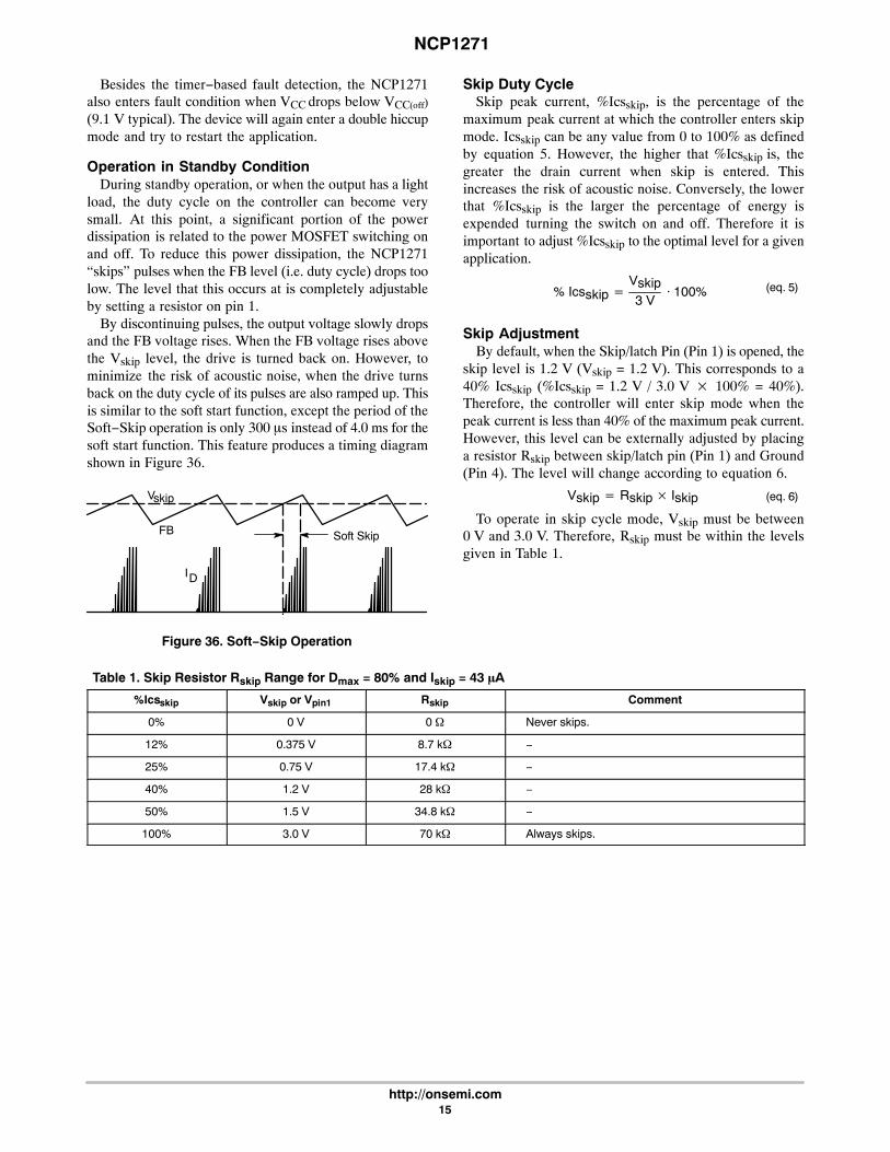
By discontinuing pulses, the output voltage slowly dropsand the FB voltage rises. When the FB voltage rises abovethe Vskip level, the drive is turned back on. However, tominimize the risk of acoustic noise, when the drive turnsback on the duty cycle of its pulses are also ramped up. Thisis similar to the soft start function, except the period of theSoft−Skip operation is only 300 �s instead of 4.0 ms for thesoft start function. This feature produces a timing diagramshown in Figure 36.
Figure 36. Soft−Skip Operation
V
FB
ID
skip
Soft Skip
Skip Duty CycleSkip peak current, %Icsskip, is the percentage of the
maximum peak current at which the controller enters skipmode. Icsskip can be any value from 0 to 100% as definedby equation 5. However, the higher that %Icsskip is, thegreater the drain current when skip is entered. Thisincreases the risk of acoustic noise. Conversely, the lowerthat %Icsskip is the larger the percentage of energy isexpended turning the switch on and off. Therefore it isimportant to adjust %Icsskip to the optimal level for a givenapplication.
% Icsskip �Vskip3 V
· 100% (eq. 5)
Skip AdjustmentBy default, when the Skip/latch Pin (Pin 1) is opened, the
skip level is 1.2 V (Vskip = 1.2 V). This corresponds to a40% Icsskip (%Icsskip = 1.2 V / 3.0 V � 100% = 40%).Therefore, the controller will enter skip mode when thepeak current is less than 40% of the maximum peak current.However, this level can be externally adjusted by placinga resistor Rskip between skip/latch pin (Pin 1) and Ground(Pin 4). The level will change according to equation 6.
Vskip � Rskip � Iskip (eq. 6)
To operate in skip cycle mode, Vskip must be between0 V and 3.0 V. Therefore, Rskip must be within the levelsgiven in Table 1.
Table 1. Skip Resistor Rskip Range for Dmax = 80% and Iskip = 43 �A
%Icsskip Vskip or Vpin1 Rskip Comment
0% 0 V 0 � Never skips.
12% 0.375 V 8.7 k� −
25% 0.75 V 17.4 k� −
40% 1.2 V 28 k� −
50% 1.5 V 34.8 k� −
100% 3.0 V 70 k� Always skips.
NCP1271
http://onsemi.com16
Recover from StandbyIn the event that a large load is encountered during skip
cycle operation, the circuit automatically disables thenormal Soft−Skip procedure and delivers maximum powerto the load (Figure 37). This feature, the Transient LoadDetector (TLD), is initiated anytime a skip event is exitedand the FB pin is greater than 2.85 V, as would be the casefor a sudden increase in output load.
Figure 37. Transient Response from Standby
VVFB
ID
skip
VTLD
load current
Maximum current availablewhen TLD level is hit
output voltage 300 �s max
External Latchoff ShutdownWhen the Skip/Latch input (Pin 1) is pulled higher than
Vlatch (8.0 V typical), the drive output is latched off untilVCC drops below VCC(reset) (4.0 Vtypical). If Vbulk staysabove approximately 30 Vdc, then the HV FET ensure thatVCC remains above VCC(latch) (5.8 Vtypical). Therefore, thecontroller is reset by unplugging the power supply from thewall and allowing Vbulk to discharge. Figure 38 illustratesthe timing diagram of VCC in the latchoff condition.
Figure 38. Latchoff VCC Timing Diagram
5.8 V
12.6 V
Startup current source ischarging the VCC capacitor
Startup current source isoff when VCC is 12.6 V
Startup current source turnson when VCC reaches 5.8 VCC
Figure 39 defines the different voltage regions of theSkip/latch Pin (Pin 1) operation.
1. When the voltage is above Vlatch (7.1 V min,8.7 V max), the circuit is in latchoff and all drivepulses are disabled until VCC cycles below 4.0 V(typical).
2. When the voltage is between Vskip−reset (5.0 Vmin, 6.5 V max) and Vlatch, the pin is considered
to be opened. The skip level Vskip is restored tothe default 1.2 V.
3. When the voltage is between about 3.0 V andVskip−reset, the Vskip level is above the normaloperating range of the feedback pin. Therefore,the output does not switch.
4. When the voltage is between 0 V and 3.0 V, theVskip is within the operating range of thefeedback pin. Then the voltage on this pin setsthe skip level as explained earlier.
Figure 39. NCP1271 Pin 1 Operating Regions
Output is latched off here.
Adjustable V range.
0 V (no skip)
3.0 V (always skip)
V pin1
8V (V )
10 V (max limit)
Output always low (skipped) here.
5.7 V (V )
Pin 1 considered to be opened.
skip−reset
latch
skip
Vskip is reset to default level 1.2 V.
The external latch feature allows the circuit designers toimplement different kinds of latching protection. TheNCP1271 applications note (AND8242/D) details severalsimple circuits to implement overtemperature protection(OTP) and overvoltage protection (OVP).
In order to prevent unexpected latchoff due to noise,it is very important to put a noise decoupling capacitornear Pin 1 to increase the noise immunity. It is alsorecommended to always have a resistor from pin 1 to GND.This further reduces the risk of premature latchoff. Alsonote that if the additional latch−off circuitry has leakage,it will modify the skip adjust setup.
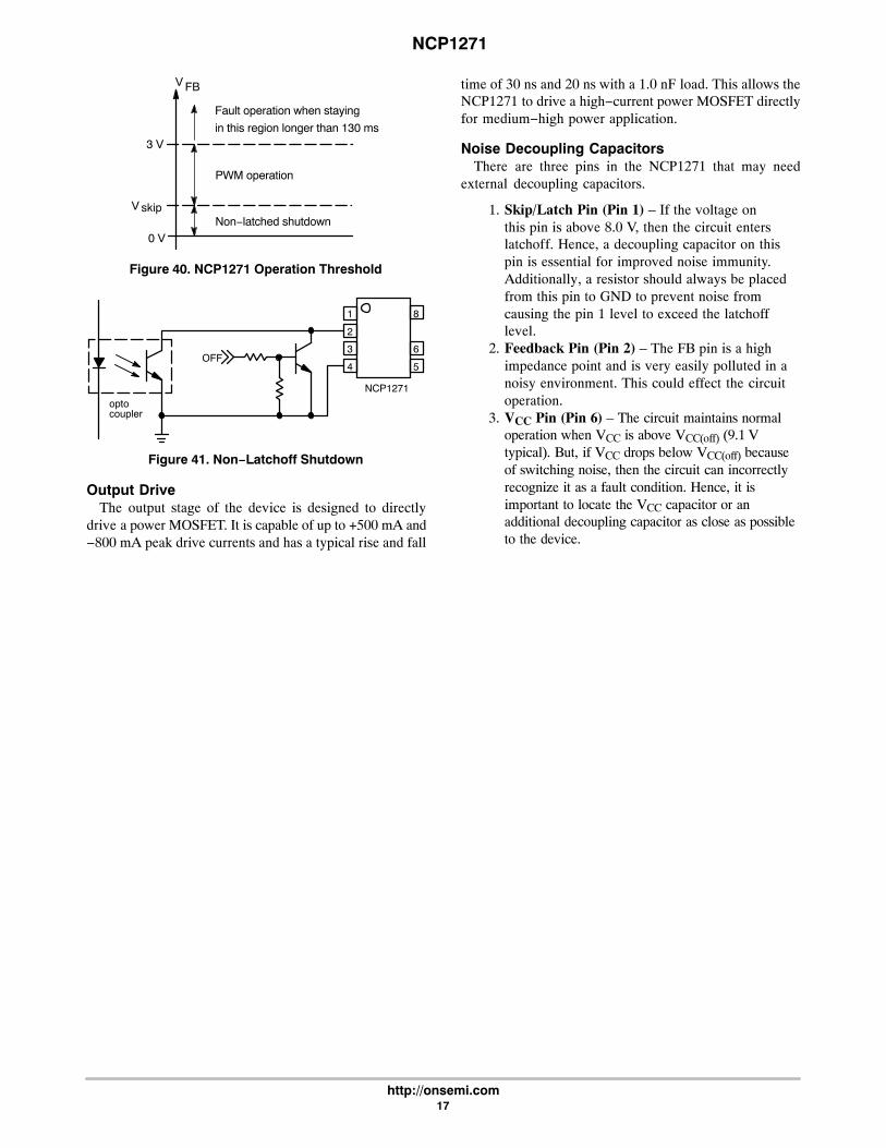
External Non−Latched ShutdownFigure 40 illustrates the Feedback (pin 2) operation. An
external non−latched shutdown can be easily implementedby simply pulling FB below the skip level. This is aninherent feature from the standby skip operation. Hence, itallows the designer to implement additional non−latchedshutdown protection.
The device can also be shutdown by pulling the VCC pinto GND (<190 mV). In addition to shutting off the output,this method also places the part into a low currentconsumption state.
NCP1271
http://onsemi.com17
Figure 40. NCP1271 Operation Threshold
Fault operation when staying
in this region longer than 130 ms
PWM operation
Non−latched shutdown
3 V
V FB
0 V
V skip
Figure 41. Non−Latchoff Shutdown
1
2
3
4
8
6
5
NCP1271
OFF
optocoupler
Output DriveThe output stage of the device is designed to directly
drive a power MOSFET. It is capable of up to +500 mA and−800 mA peak drive currents and has a typical rise and fall
time of 30 ns and 20 ns with a 1.0 nF load. This allows theNCP1271 to drive a high−current power MOSFET directlyfor medium−high power application.
Noise Decoupling CapacitorsThere are three pins in the NCP1271 that may need
external decoupling capacitors.
1. Skip/Latch Pin (Pin 1) – If the voltage onthis pin is above 8.0 V, then the circuit enterslatchoff. Hence, a decoupling capacitor on thispin is essential for improved noise immunity.Additionally, a resistor should always be placedfrom this pin to GND to prevent noise fromcausing the pin 1 level to exceed the latchofflevel.
2. Feedback Pin (Pin 2) – The FB pin is a highimpedance point and is very easily polluted in anoisy environment. This could effect the circuitoperation.
3. VCC Pin (Pin 6) – The circuit maintains normaloperation when VCC is above VCC(off) (9.1 Vtypical). But, if VCC drops below VCC(off) becauseof switching noise, then the circuit can incorrectlyrecognize it as a fault condition. Hence, it isimportant to locate the VCC capacitor or anadditional decoupling capacitor as close as possibleto the device.
NCP1271
http://onsemi.com18
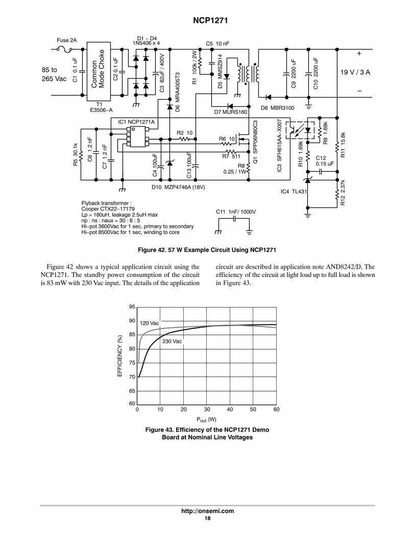
Figure 42. 57 W Example Circuit Using NCP1271
IC1 NCP1271A
+
−
85 to265 Vac
19 V / 3 A
Com
mon
Mod
e C
hoke
D8 MBR3100
R1
100
k / 2
W
R5
30.
1k
E3506−A D6
MR
A40
05T
3
1N5406 x 4
D7 MURS160
R7 511
R9
1.6
9k
C3
82u
F /
400V
IC4 TL431
Q1
SP
P06
N80
C3
0.25 / 1W
D5
MM
SZ
914
C4
100u
F
R2 10
D10 MZP4746A (18V)
R10
1.6
9kC
9 2
200
uF
C10
220
0 uF
R6 10
IC3
SF
H61
5AA−X
007
C5 10 nF
Flyback transformer :Cooper CTX22−17179Lp = 180uH, leakage 2.5uH maxnp : ns : naux = 30 : 6 : 5Hi−pot 3600Vac for 1 sec, primary to secondaryHi−pot 8500Vac for 1 sec, winding to core
C120.15 uF
C7
1.2
nF
C6
1.2
nF
C2
0.1
uF
T1
C1
0.1
uF
D1 − D4
R12
2.3
7kR
11 1
5.8k
C11 1nF/ 1000V
R8
Fuse 2A
C13
100
uF
Figure 42 shows a typical application circuit using theNCP1271. The standby power consumption of the circuitis 83 mW with 230 Vac input. The details of the application
circuit are described in application note AND8242/D. Theefficiency of the circuit at light load up to full load is shownin Figure 43.
Figure 43. Efficiency of the NCP1271 DemoBoard at Nominal Line Voltages
Pout (W)
6050403020060
65
70
75
80
85
90
EF
FIC
IEN
CY
(%
)
10
95
230 Vac
120 Vac
NCP1271
http://onsemi.com19
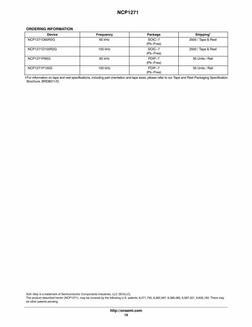
ORDERING INFORMATIONDevice Frequency Package Shipping†
NCP1271D65R2G 65 kHz SOIC−7(Pb−Free)
2500 / Tape & Reel
NCP1271D100R2G 100 kHz SOIC−7(Pb−Free)
2500 / Tape & Reel
NCP1271P65G 65 kHz PDIP−7(Pb−Free)
50 Units / Rail
NCP1271P100G 100 kHz PDIP−7(Pb−Free)
50 Units / Rail
†For information on tape and reel specifications, including part orientation and tape sizes, please refer to our Tape and Reel Packaging SpecificationBrochure, BRD8011/D.
Soft−Skip is a trademark of Semiconductor Components Industries, LLC (SCILLC).The product described herein (NCP1271), may be covered by the following U.S. patents: 6,271,735, 6,362,067, 6,385,060, 6,597,221, 6,633,193. There maybe other patents pending.
PDIP−7 (PDIP−8 LESS PIN 7)CASE 626B
ISSUE DDATE 22 APR 2015
STYLE 1:PIN 1. AC IN
2. DC + IN3. DC − IN4. AC IN5. GROUND6. OUTPUT7. NOT USED8. VCC
SCALE 1:1
1 4
58
b2NOTE 8
D
b
L
A1
A
eB
XXXXXXXXXAWL
YYWWG
E
GENERICMARKING DIAGRAM*
XXXX = Specific Device CodeA = Assembly LocationWL = Wafer LotYY = YearWW = Work WeekG = Pb−Free Package
*This information is generic. Please refer todevice data sheet for actual part marking.Pb−Free indicator, “G” or microdot “ �”,may or may not be present.
A
TOP VIEW
C
SEATINGPLANE
0.010 C ASIDE VIEW
END VIEW
END VIEW
WITH LEADS CONSTRAINED
NOTES:1. DIMENSIONING AND TOLERANCING PER ASME Y14.5M, 1994.2. CONTROLLING DIMENSION: INCHES.3. DIMENSIONS A, A1 AND L ARE MEASURED WITH THE PACK-
AGE SEATED IN JEDEC SEATING PLANE GAUGE GS−3.4. DIMENSIONS D, D1 AND E1 DO NOT INCLUDE MOLD FLASH
OR PROTRUSIONS. MOLD FLASH OR PROTRUSIONS ARENOT TO EXCEED 0.10 INCH.
5. DIMENSION E IS MEASURED AT A POINT 0.015 BELOW DATUMPLANE H WITH THE LEADS CONSTRAINED PERPENDICULARTO DATUM C.
6. DIMENSION eB IS MEASURED AT THE LEAD TIPS WITH THELEADS UNCONSTRAINED.
7. DATUM PLANE H IS COINCIDENT WITH THE BOTTOM OF THELEADS, WHERE THE LEADS EXIT THE BODY.
8. PACKAGE CONTOUR IS OPTIONAL (ROUNDED OR SQUARECORNERS).
E1
M
8X
c
D1
B
H
NOTE 5
e
e/2A2
NOTE 3
M B M NOTE 6
M
DIM MIN MAXINCHES
A −−−− 0.210A1 0.015 −−−−
b 0.014 0.022
C 0.008 0.014D 0.355 0.400D1 0.005 −−−−
e 0.100 BSC
E 0.300 0.325
M −−−− 10
−−− 5.330.38 −−−
0.35 0.56
0.20 0.369.02 10.160.13 −−−
2.54 BSC
7.62 8.26
−−− 10
MIN MAXMILLIMETERS
E1 0.240 0.280 6.10 7.11
b2
eB −−−− 0.430 −−− 10.92
0.060 TYP 1.52 TYP
A2 0.115 0.195 2.92 4.95
L 0.115 0.150 2.92 3.81°°
MECHANICAL CASE OUTLINE
PACKAGE DIMENSIONS
ON Semiconductor and are trademarks of Semiconductor Components Industries, LLC dba ON Semiconductor or its subsidiaries in the United States and/or other countries.ON Semiconductor reserves the right to make changes without further notice to any products herein. ON Semiconductor makes no warranty, representation or guarantee regardingthe suitability of its products for any particular purpose, nor does ON Semiconductor assume any liability arising out of the application or use of any product or circuit, and specificallydisclaims any and all liability, including without limitation special, consequential or incidental damages. ON Semiconductor does not convey any license under its patent rights nor therights of others.
98AON12198DDOCUMENT NUMBER:
DESCRIPTION:
Electronic versions are uncontrolled except when accessed directly from the Document Repository.Printed versions are uncontrolled except when stamped “CONTROLLED COPY” in red.
PAGE 1 OF 1PDIP−7 (PDIP−8 LESS PIN 7)
© Semiconductor Components Industries, LLC, 2019 www.onsemi.com
SOIC−7CASE 751U−01
ISSUE EDATE 20 OCT 2009
SEATINGPLANE
14
58
R
J
X 45�
K
NOTES:1. DIMENSIONING AND TOLERANCING PER
ANSI Y14.5M, 1982.2. CONTROLLING DIMENSION: MILLIMETER.3. DIMENSION A AND B ARE DATUMS AND T
IS A DATUM SURFACE.4. DIMENSION A AND B DO NOT INCLUDE
MOLD PROTRUSION.5. MAXIMUM MOLD PROTRUSION 0.15 (0.006)
PER SIDE.
S
DH
C
SCALE 1:1
DIMA
MIN MAX MIN MAXINCHES
4.80 5.00 0.189 0.197
MILLIMETERS
B 3.80 4.00 0.150 0.157C 1.35 1.75 0.053 0.069D 0.33 0.51 0.013 0.020G 1.27 BSC 0.050 BSCH 0.10 0.25 0.004 0.010J 0.19 0.25 0.007 0.010K 0.40 1.27 0.016 0.050M 0 8 0 8 N 0.25 0.50 0.010 0.020S 5.80 6.20 0.228 0.244
−A−
−B−
G
MBM0.25 (0.010)
−T−
BM0.25 (0.010) T S A S
M
XXX = Specific Device CodeA = Assembly LocationL = Wafer LotY = YearW = Work Week� = Pb−Free Package
GENERICMARKING DIAGRAM
7 PL� � � �
*This information is generic. Please refer todevice data sheet for actual part marking.Pb−Free indicator, “G” or microdot “ �”,may or may not be present.
XXXXXALYWX
�1
8
STYLES ON PAGE 2
1.520.060
7.00.275
0.60.024
1.2700.050
4.00.155
� mminches
�SCALE 6:1
*For additional information on our Pb−Free strategy and solderingdetails, please download the ON Semiconductor Soldering andMounting Techniques Reference Manual, SOLDERRM/D.
SOLDERING FOOTPRINT*
MECHANICAL CASE OUTLINE
PACKAGE DIMENSIONS
ON Semiconductor and are trademarks of Semiconductor Components Industries, LLC dba ON Semiconductor or its subsidiaries in the United States and/or other countries.ON Semiconductor reserves the right to make changes without further notice to any products herein. ON Semiconductor makes no warranty, representation or guarantee regardingthe suitability of its products for any particular purpose, nor does ON Semiconductor assume any liability arising out of the application or use of any product or circuit, and specificallydisclaims any and all liability, including without limitation special, consequential or incidental damages. ON Semiconductor does not convey any license under its patent rights nor therights of others.
98AON12199DDOCUMENT NUMBER:
DESCRIPTION:
Electronic versions are uncontrolled except when accessed directly from the Document Repository.Printed versions are uncontrolled except when stamped “CONTROLLED COPY” in red.
PAGE 1 OF 27−LEAD SOIC
© Semiconductor Components Industries, LLC, 2019 www.onsemi.com
SOIC−7CASE 751U−01
ISSUE EDATE 20 OCT 2009
STYLE 4:PIN 1. ANODE
2. ANODE3. ANODE4. ANODE5. ANODE6. ANODE7. NOT USED8. COMMON CATHODE
STYLE 1:PIN 1. EMITTER
2. COLLECTOR3. COLLECTOR4. EMITTER5. EMITTER6.7. NOT USED8. EMITTER
STYLE 2:PIN 1. COLLECTOR, DIE, #1
2. COLLECTOR, #13. COLLECTOR, #24. COLLECTOR, #25. BASE, #26. EMITTER, #27. NOT USED8. EMITTER, #1
STYLE 3:PIN 1. DRAIN, DIE #1
2. DRAIN, #13. DRAIN, #24. DRAIN, #25. GATE, #26. SOURCE, #27. NOT USED8. SOURCE, #1
STYLE 6:PIN 1. SOURCE
2. DRAIN3. DRAIN4. SOURCE5. SOURCE6.7. NOT USED8. SOURCE
STYLE 5:PIN 1. DRAIN
2. DRAIN3. DRAIN4. DRAIN5.6.7. NOT USED8. SOURCE
STYLE 7:PIN 1. INPUT
2. EXTERNAL BYPASS3. THIRD STAGE SOURCE4. GROUND5. DRAIN6. GATE 37. NOT USED8. FIRST STAGE Vd
STYLE 8:PIN 1. COLLECTOR (DIE 1)
2. BASE (DIE 1)3. BASE (DIE 2)4. COLLECTOR (DIE 2)5. COLLECTOR (DIE 2)6. EMITTER (DIE 2)7. NOT USED8. COLLECTOR (DIE 1)
STYLE 9:PIN 1. EMITTER (COMMON)
2. COLLECTOR (DIE 1)3. COLLECTOR (DIE 2)4. EMITTER (COMMON)5. EMITTER (COMMON)6. BASE (DIE 2)7. NOT USED8. EMITTER (COMMON)
STYLE 10:PIN 1. GROUND
2. BIAS 13. OUTPUT4. GROUND5. GROUND6. BIAS 27. NOT USED8. GROUND
STYLE 11:PIN 1. SOURCE (DIE 1)
2. GATE (DIE 1)3. SOURCE (DIE 2)4. GATE (DIE 2)5. DRAIN (DIE 2)6. DRAIN (DIE 2)7. NOT USED8. DRAIN (DIE 1)
ON Semiconductor and are trademarks of Semiconductor Components Industries, LLC dba ON Semiconductor or its subsidiaries in the United States and/or other countries.ON Semiconductor reserves the right to make changes without further notice to any products herein. ON Semiconductor makes no warranty, representation or guarantee regardingthe suitability of its products for any particular purpose, nor does ON Semiconductor assume any liability arising out of the application or use of any product or circuit, and specificallydisclaims any and all liability, including without limitation special, consequential or incidental damages. ON Semiconductor does not convey any license under its patent rights nor therights of others.
98AON12199DDOCUMENT NUMBER:
DESCRIPTION:
Electronic versions are uncontrolled except when accessed directly from the Document Repository.Printed versions are uncontrolled except when stamped “CONTROLLED COPY” in red.
PAGE 2 OF 27−LEAD SOIC
© Semiconductor Components Industries, LLC, 2019 www.onsemi.com
onsemi, , and other names, marks, and brands are registered and/or common law trademarks of Semiconductor Components Industries, LLC dba “onsemi” or its affiliatesand/or subsidiaries in the United States and/or other countries. onsemi owns the rights to a number of patents, trademarks, copyrights, trade secrets, and other intellectual property.A listing of onsemi’s product/patent coverage may be accessed at www.onsemi.com/site/pdf/Patent−Marking.pdf. onsemi reserves the right to make changes at any time to anyproducts or information herein, without notice. The information herein is provided “as−is” and onsemi makes no warranty, representation or guarantee regarding the accuracy of theinformation, product features, availability, functionality, or suitability of its products for any particular purpose, nor does onsemi assume any liability arising out of the application or useof any product or circuit, and specifically disclaims any and all liability, including without limitation special, consequential or incidental damages. Buyer is responsible for its productsand applications using onsemi products, including compliance with all laws, regulations and safety requirements or standards, regardless of any support or applications informationprovided by onsemi. “Typical” parameters which may be provided in onsemi data sheets and/or specifications can and do vary in different applications and actual performance mayvary over time. All operating parameters, including “Typicals” must be validated for each customer application by customer’s technical experts. onsemi does not convey any licenseunder any of its intellectual property rights nor the rights of others. onsemi products are not designed, intended, or authorized for use as a critical component in life support systemsor any FDA Class 3 medical devices or medical devices with a same or similar classification in a foreign jurisdiction or any devices intended for implantation in the human body. ShouldBuyer purchase or use onsemi products for any such unintended or unauthorized application, Buyer shall indemnify and hold onsemi and its officers, employees, subsidiaries, affiliates,and distributors harmless against all claims, costs, damages, and expenses, and reasonable attorney fees arising out of, directly or indirectly, any claim of personal injury or deathassociated with such unintended or unauthorized use, even if such claim alleges that onsemi was negligent regarding the design or manufacture of the part. onsemi is an EqualOpportunity/Affirmative Action Employer. This literature is subject to all applicable copyright laws and is not for resale in any manner.
PUBLICATION ORDERING INFORMATIONTECHNICAL SUPPORTNorth American Technical Support:Voice Mail: 1 800−282−9855 Toll Free USA/CanadaPhone: 011 421 33 790 2910
LITERATURE FULFILLMENT:Email Requests to: [email protected]
onsemi Website: www.onsemi.com
Europe, Middle East and Africa Technical Support:Phone: 00421 33 790 2910For additional information, please contact your local Sales Representative
◊
![PWM Solar Charge Controller filePWM Solar Charge Controller ... Anti-reverse connection protection make there is no reversely charging in night. ... Consumption at standby [mA]](https://img.pdfslide.us/doc/110x75/5c87e0dc09d3f24c348cb092/pwm-solar-charge-controller-solar-charge-controller-anti-reverse-connection.jpg)