Embed Size (px)
Citation preview
NAVAL POSTGRADUATE SCHOOLSMo n te r e y , C a lifo rn ia D TIC F LL C O P Y
DTIC-AELECTE
SOCT0 2.19870
THESISVIE USE OF COAXIAL TRANSMISSION LINE
ELEMENTSIN LOG-PERIODIC DIPOLE ARRAYS
by
Robert E. Tarleton, Jr.
June 1987
Thesiz Advisor R.chard W. Adler
Approved for public r'elease; distribution is unlimited.
o
r~

fl(RIjNI Ct hS.EIIATION 0$ r,41¶ PAGE
REPORT- DOCUMENTATION PAGEIj Rf PORT `IECURI.Y CLASISICATI0N tb RESTRICTIVE MARKINGSUNCLASSIFIED
2,1 WIbR'ty CLASSIFICATION AutWORIty 3 0ISTRIRUrIONJAVAILIA$ILItY Of R(PQRT
1b OECLLASSIFICATION /OOWNGSIAOING S~4WL Approved for public release;distribution unlimited
3 PERFORMING. ORGANIZATION REPORT NUMBER(S) IS MONITORING ORGANIZATION RkEPORr NUVOER(S)
6& NAME OF PERFORMING ORGANIZATION 60E O$$ICE SVIVSOL ?a NAME OF MONIroRNG ORGANIZATION
Naval Postgraduate School I Code 62 Naval Postgraduate School
6< AOORE$SS i~v Stato. e.d ZIP Cod#) lb A.OOA(SS(City. Stee. j'*d VP Cod).J
Monterey, California 93943-5000 Monterey, California 9-3943-5000
S& NAVE 06 1UNOING, SPONSORING lb 'ThICt SjyAA L PROCUREWEr -INS 1ROI)MNI TIONI(AtIOP.IJN".)RGANtNAtION - IeoicbJ
PIC 'OO0Es W-4'I Vftet on V.~e10 3 [IQ) SQI)RCE 0f fkNOING NUMVIUS
PIICRGRAMi PRO;ECT TMSK OI)RWe 'Nit
IL hICTft"AAJMNT NO* NO NO ACCE 1501 NIO
THE USE OF COAXIAL TRANSMISSION LINE ELEMENTS IN LOG-PERIODIC DIPOLFARRAYS
Tgr~leon. Bobert E.. Jr.* I,,'t -4 *IV'ORt 113 ' e.4( CelVVI 40 W1 ~ E Of I*EII0T (Yost W.PAtA 04y) C~A(, I)- 14
* Mstebs 1ijs I `10"A '0 __119P7 June 1170
COSAI? COD($¶ I1 SUMICI 1141-AS lCow-tvii ch ltve'we I$ m#c4pue. erP d woi tý riv wo'T flu-Ybo
10 G;u ueGOj Log-periodic dipole array, k-beta diagram,.Snyder dipole, Numerical Electromagnetics Code
I AWRA(I~i (Co'N's.~* OA '9ipt4e it notpiijr df "A#$ff Wqj AJiob oute
This thesis examines' the feasibility of designing a log-periodicdipole array (LPDA) with ccaxial. transmission line elements andcomparing the resulting operational bandwidth with that of aconventional. LPDA. Using the Numerical Electromagnetic s Code (NEC), acoaxial dipole was modeled to optimize the bandwidth and then u3n-d asthie element in a variety of uniform arrays. Different t7pes of elemernetconnections were examined including switched series, switched par~allel,and unswitched parallel.. The results of NEC for each of the arrays areplotted as k-fl diagrams to compare to the standard arrays.
The results of the investigAtion show that the Snyder dipoleprovides more operational bandwidth than a standard dipole, but whenplaced in a uniform array there is no more bandwidth than that of aconventional uniform array._
if 1 'OjAvAILAIlt.Tv 0 AgitUAC? 21 AqSVIACt I? N
"(%S$'0htM M 3SAI41A 4f 00, ýtj UNCLASSIFIlED _____
410tl %100 fiAMI -A5 A.f 0i-C 100
A. o,.r . Adler (48)6-3 52 62Pb14) P~.i~*...*~t~g~4B#6 ~~(**~, L.
All 00-0 944 0o Ste~ut~ U01001
Approved for public release; distribution is unlimited.
"The Use of Coaxial Transmission Line Elementsin Log-periodic Dipole Arrays
by
Robert E. Tarleton, Jr.Electronic Engineer, Department of Defense
B.S.E., Arizona State University, 1980
Submitted in partial fulfillment of the
requirements for the degree of
MASTER OF SCIENCE IN ELECTRICAL ENGINEERING
from the
NAVAL POSTGRADUATE SCHOOLJune 1987
Author: 27Robert E.&Trleton Jr. "'
Approved by-.,,SRichard W.Adler, Thesis Ad _or _
W. Ray Vihcent, Secodd Reader
"•_\Johin P. Powers, chairman, "Departmied of Electrical and Computer Engineering
(Gordon E. Schacher,
Dean of Science and Engineering
2

ABSTRACT
This thesis examines the feasibility of designing a log-periodic dipole array
(LPDA) with coaxial transmission line elements and comparing the resultingoperational bandwidth with that of a conventional LPDA. Using the NumericalElectromagnetics Code (NEC), a coaxial dipole was modeled to optimize thebandwidth and then used as the element in a variety of uniform arrays. Different typesof element connections were examined including switched series, switched parallel, and
unswitched parallel. The results of NEC for each of the arrays are plotted as k-p-'diagrams to compare to the standard arrays.
The results of the investigation show that the Snyder dipole provides more
operational bandwidth than a standard dipole, but when placed in a uniform array
there is no more bandwidth than that of a conventional uniform array.
/7
"Accesion ForNTIS CRA&I
= ~ OTIC TAB
By ...
i Avuil .t 1or0!
3
TABLE OF CONTENTS
. INTRODUCTION ..... ".................. 8A. THE LOG-PERIODIC ANTENNA ........................... 8B. THE LOG-PERIODIC DIPOLE ARRAY ...................... 9.C. CHARACTERISTICS OF SUCCESSFUL LOG-
PERIODIC ANTENNAS .................................. 11D. THE LPDA WITH COAXIAL ELEMENTS ................... 11
II. DEVELOPMENT OF THE SNYDER DIPOLE ..................... 13
A. THE NUMERICAL ELECTROMAGNETICS CODE .......... 13B. PROCEDURE FOR OBTAINING OPTIMUM SNYDER
DIPOLE ..... .. . .................................................... 13
III. K-BETA DIAGRAMS ........................................ 17
A. K-BETA DIAGRAM DESCRIPTION ........................ 17
B. OBTAINING THE K-BETA DIAGRAM DATA USINGN EC ...................... ,............................. .18
IV. EXPERIMENTAL PROCEDURES AND RESULTS ............... 20A. CHARACTERISTICS OF UNTAPERED ARRAYS ......... 20B. DEVELOPMN *OF T.N ERLPDA................ 20A R T . .... i i ..... .. ....... ......2C. E1CPER~INEN'A p~E~I'S...,........,........*...2
1, Switched S•ie Asra ...,.. ..... ,........212. Switched Pazal•el Array ............................. 23
3. Umnwitched Paralll Array ........................... 32D., COMPARISON OF SNYDER ARRAY TO
CONVENTIONAL ARRAY ................................ 32.
V. CONCLUSIONS AND RECOMMENDATIONS ...................
APPENDIX A: NEC DATA SETS ................................... 46
4

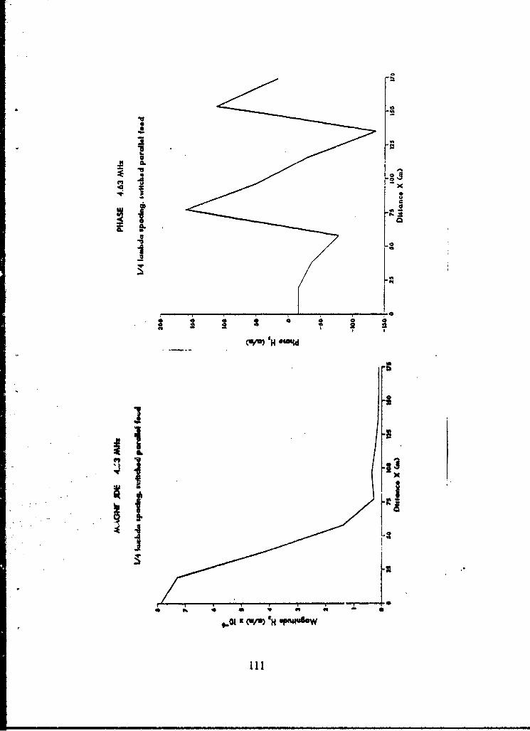
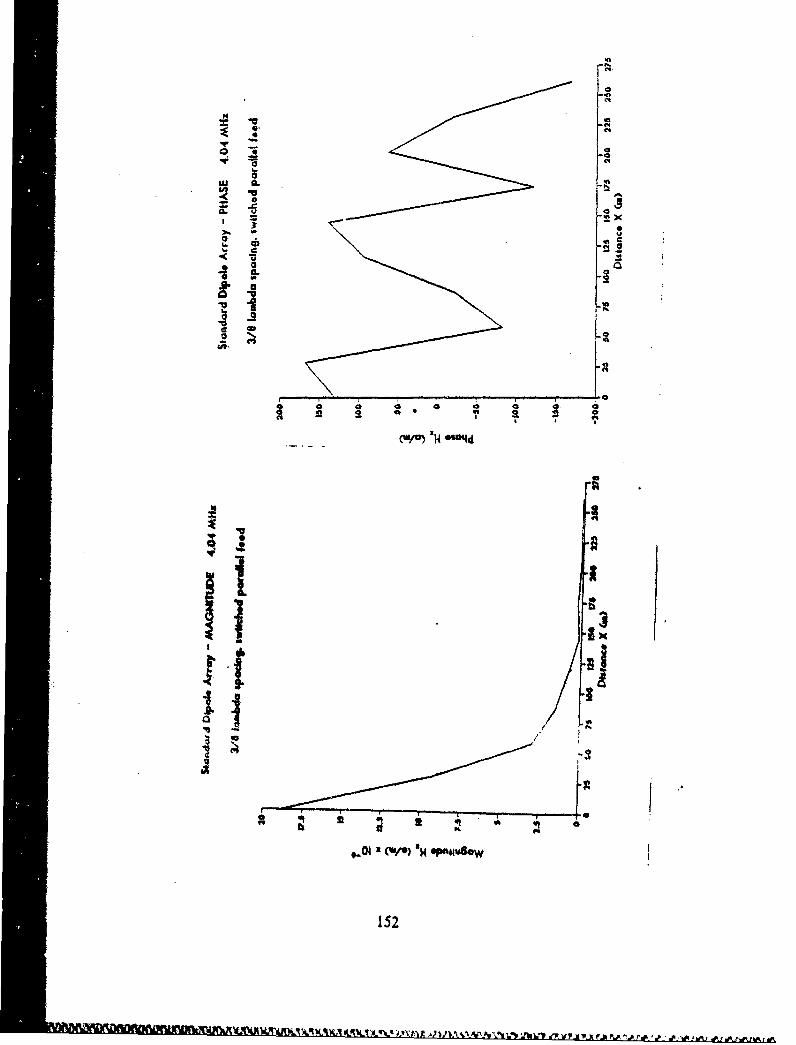
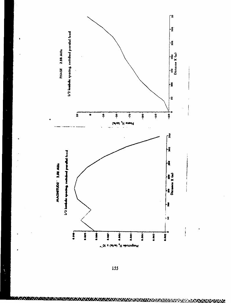
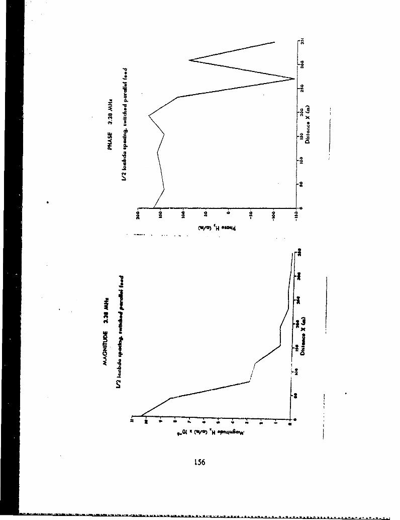
APPENDIX B: NEAR-MAGNETIC FIELD PLOTS FOR SNYDERSWITCHED SERIES ARRAYS .......................... 48
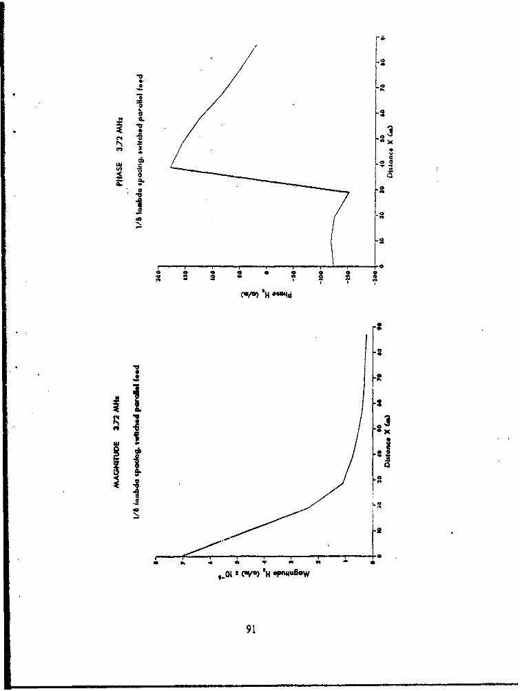
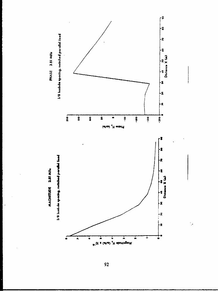
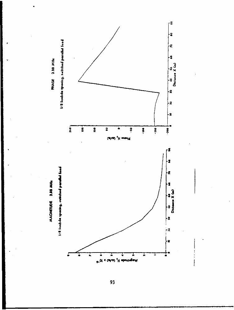
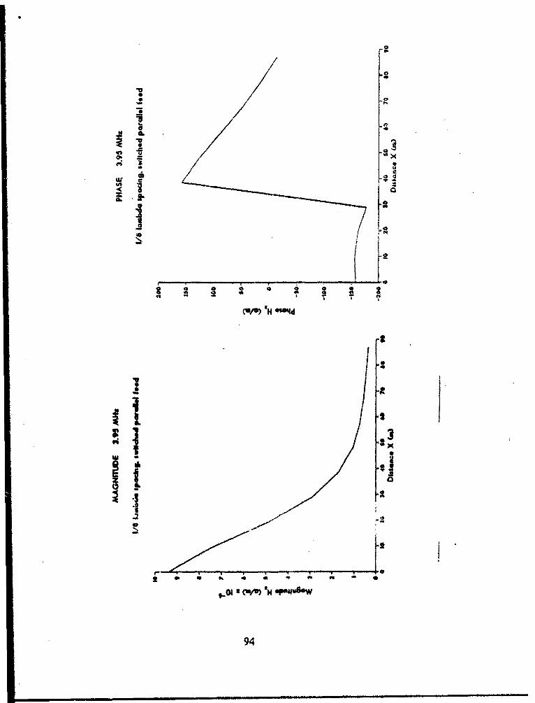
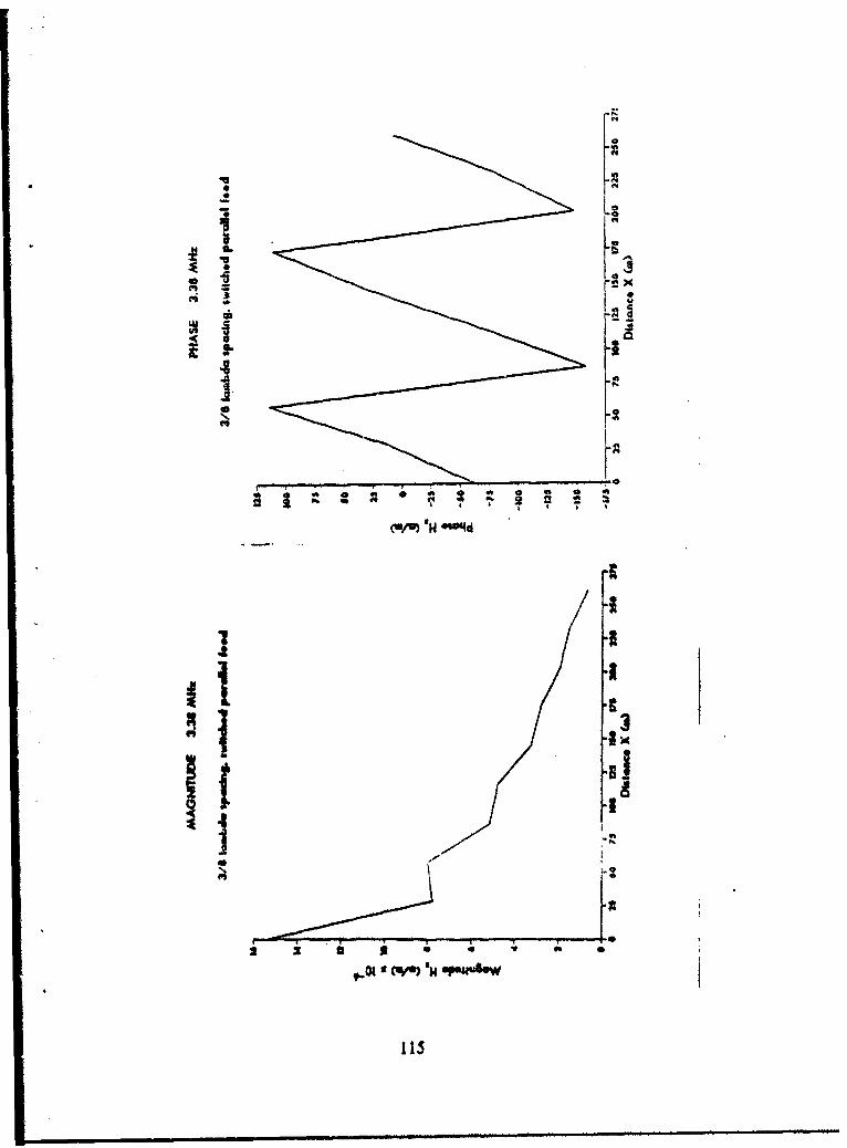
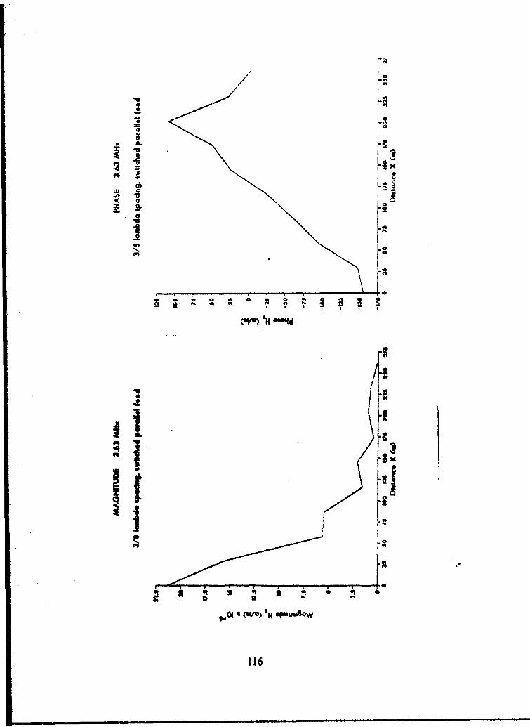
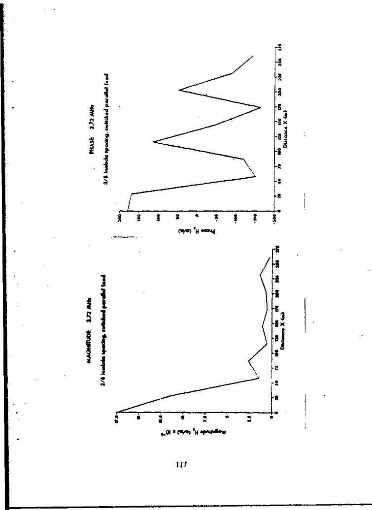
APPENDIX C: NEAR-MAGNETIC. FIELD PLOTS FOR SNYDERSWITCHED PARALLEL ARRAYS ....................... 87
APPENDIX D: NEAR-MAGNETIC FIELD PLOTS FOR SNYDERUNSWITCHED PARALLEL ARRAY ..................... 132
SAPPENDIX E: NEAR-MAGNETIC FIELD PLOTS FOR STANDARD
ELEMENT ARRAYS .................................. 147
LIST OF REFERENCES ............................................... 162
INITIAL DISTRIBUTION LIST ........................................ 163
5
LIST OF FIGURES
1.1 Log-periodic Toothed Planar Antenna (from Ref. 2) ..................... 91.2 Log-periodic Dipole Array (from Ref. 2) .............................. 101.3 Connection of LPDA Elements (from Ref. 3) ......................... 101.4 The Snyder Dipole (from Ref. 5) .................................... 12
2.1 Dipole and Transmission Line Susceptances ........................... 152.2 Standard Dipole and Snyder Dipole Bandwidths ........................ 16
3.1 k-I) Diagram (from Ref. 8) ....................... ...... 17
4.1 Types of Voltage Feed ............................................ 224.2 k-] Diagram for a Snyder Switched Series Array. Element Spacing -
1/8 W avelength .................................................. 244.3 Attenuation of a Snyder Switched Series Array. Element Spacing ,
118 W avelength ....................................... .......... 254.4 k-P Diagram for a Snyder Switched Series Array. Element Spacing -
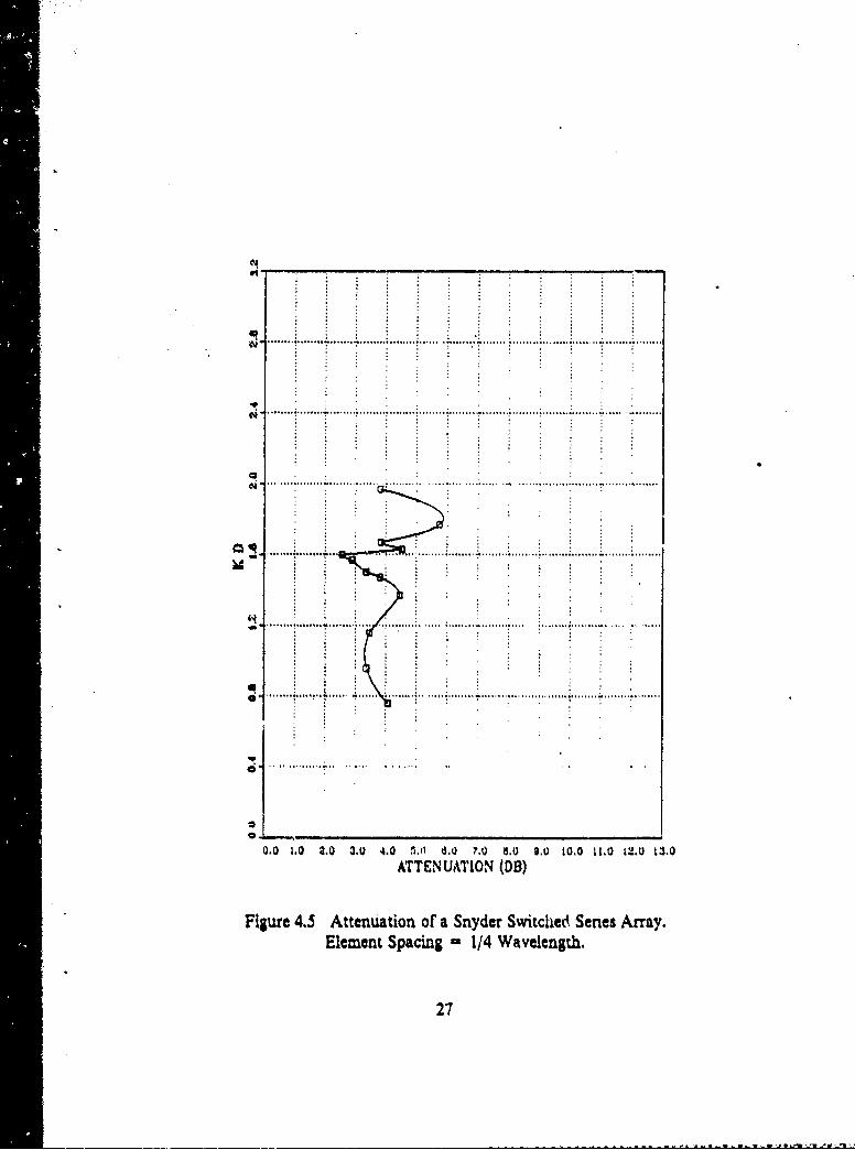
1/4 W avelength .................................................. 264.5 Attenuation of a Snyder Switched Series Array, Element Spacing -
1/4 W avelength .................................................. 27
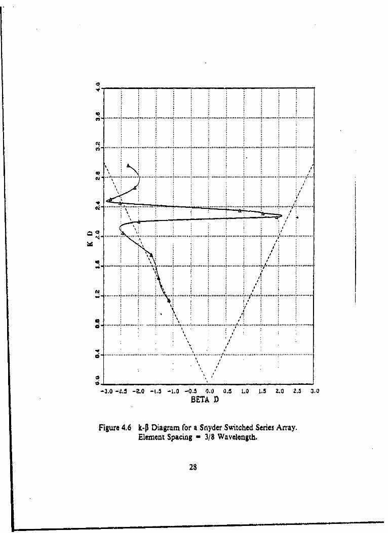
4.6 k-P Diagram for a Snyder Switched Series Array. Element Spacing -3;8 W avelength .......... .............. ................... 28
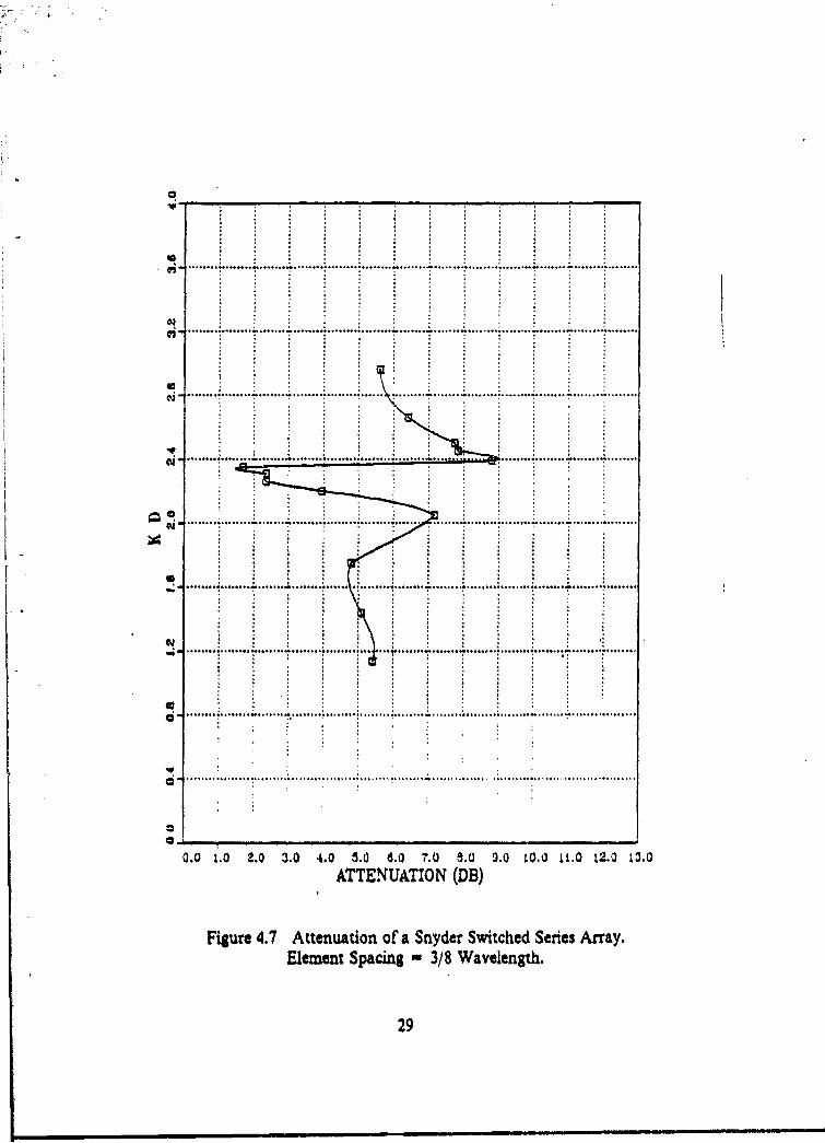
4.7 Attenuation of a Snyder Switched Series Array. Element Spacing -3/8 W avelength ........................... ...................... 29
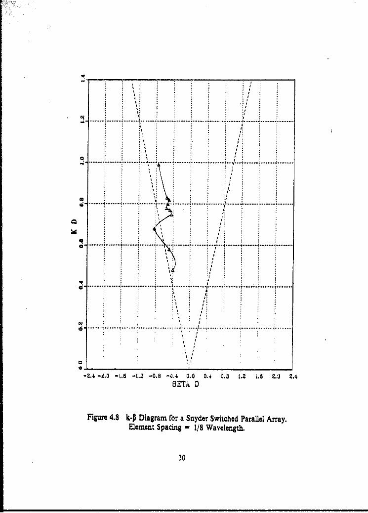
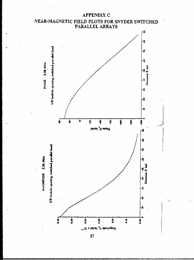
4.8 k-P Diagram for a Snyder Switched Parallel Array. Element Spacing- 1/8 W avelength ................................................ 30
4.9 Attenuation of a Snyder Switched Parallel Array. Element Spacing -118 W avelength .................................................. 31
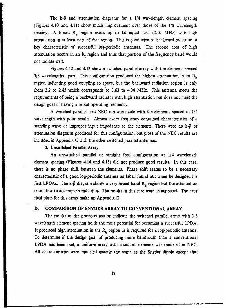
4.10 k-P Diagram for a Snyder Switched Parallel Array. Element SpacingS1a14 Wavelength ........................................ 33
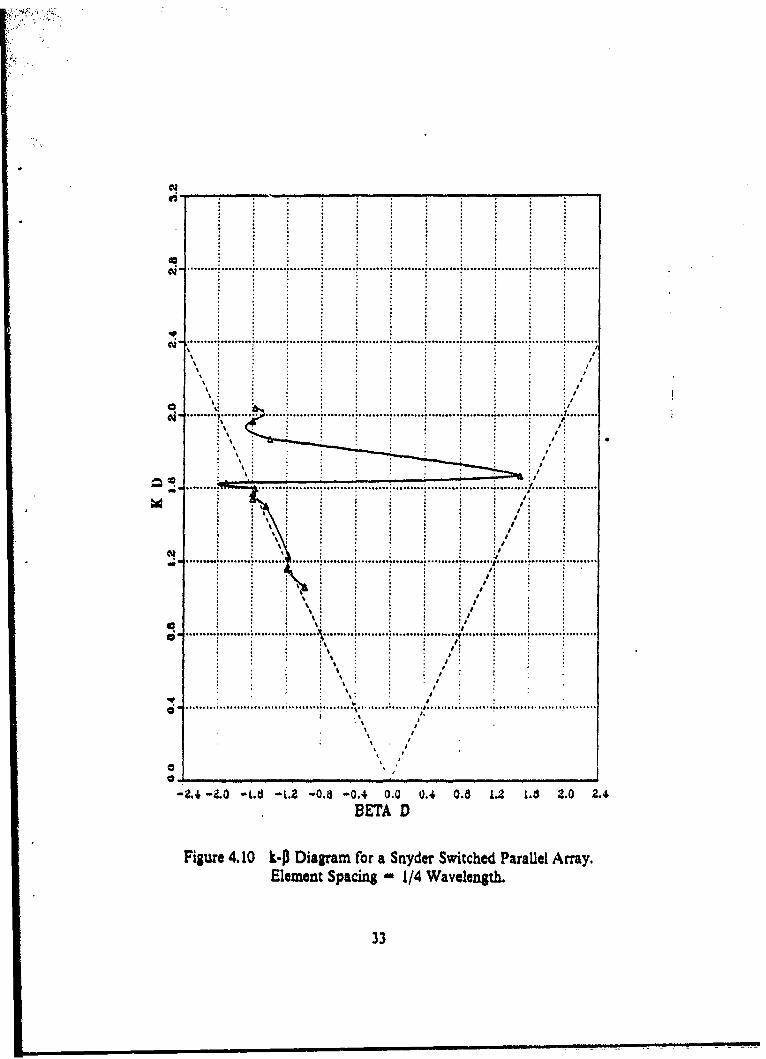
4.11 Attenuation of a Snyder Switched Parallel Array. Element Spacing -1:4 W avelength ..................................... ............ 34
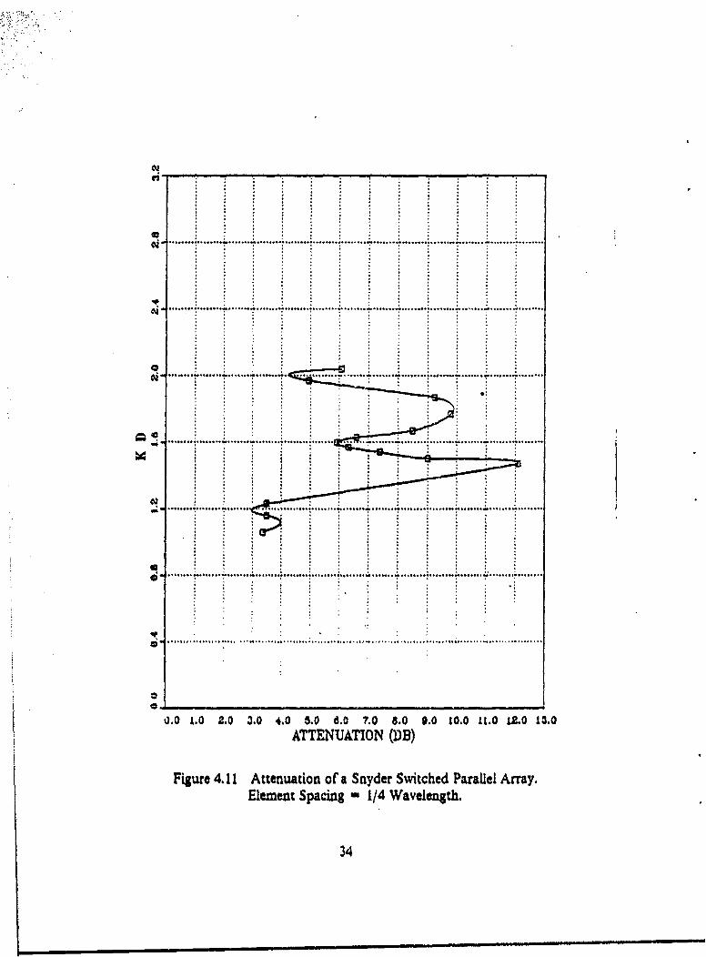
4.12 k-P Diagram for a Snyder Switched Parallel Array. Element Spacing- 3/8 W avelength ...................................... ......... 35
4.13 Attenuation of a Snyder Switched Parallel Array. Element Spacing -318 W avelength .................................................. 36
6
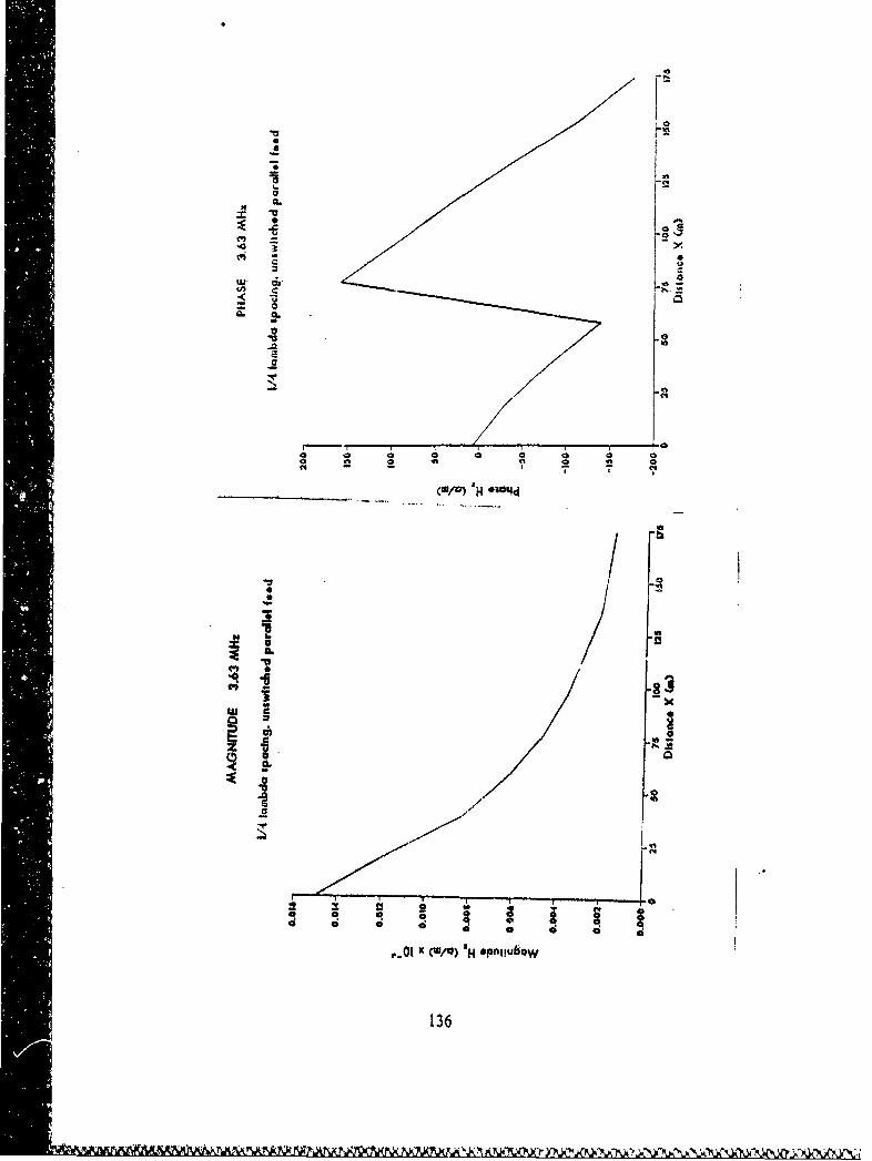
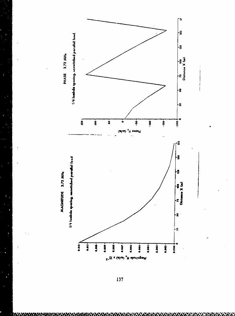
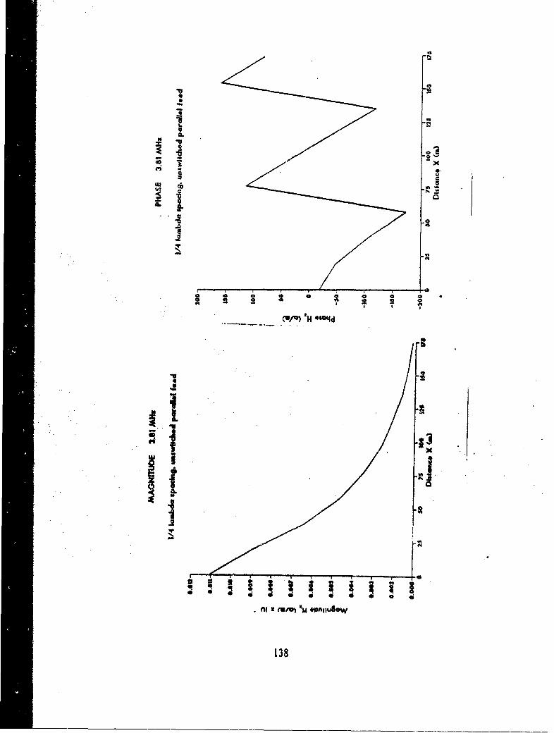
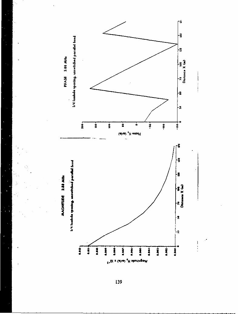
4.14 k-0 Diagram for a Snyder Unswitched Parallel Array. ElementSpacing - 1/4 W avelength ......................................... 37
4.15 Attenuation of a Snyder Unswitched Parallel Array. Element Spacing- 1/4 W avelength ................................................. 38
4.16 k-J3 Diagrain for a Standard Switched Parallel Array. ElementSpacing = 3/8 W avelength ........................................ 40
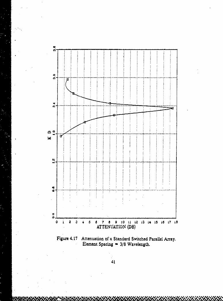
4.17 Attenuation of a Standard Switched Parallel Array. Element Spacing- 3/8 W avelength ................................................ 41
4.18 k-P Diagram Comparison .......................................... 42
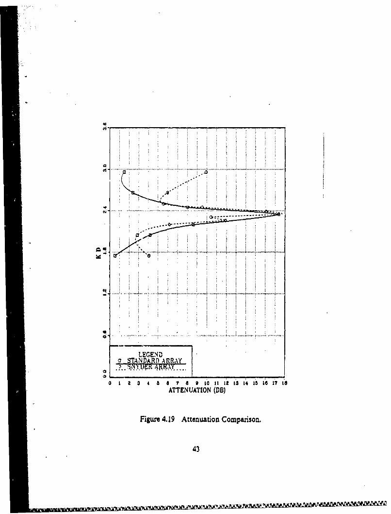
4.19 Attenuation Comparison ....... ........................ 43
7
L INTRODUCTION
A. THE LOG-PERIODIC ANTENNA
The log-periodic antenna (LPA) is structured so that its impedance and radiation
characteristics repeat periodically as the logarithm of frequency. The variations over
the operational frequency are minor so that the LPA is considered to be frequency
independent.
The LPA design is based on relatively simple ideas that produce bandwidths of
operation that were considered impossible several decades ago. One of these ideas is
the angle condition which specifies an ante-nwa array by angles only and not by specific
dimensions. In this case the antenna is self-scaling and eliminates the dependence on
its characteristic length and operating frequency. The second idea is that if an antenna
array's dimensions are scaled by a factor r, it will exhibit the same properties at one
frequency as at t times that frequency. These properties are a periodic function of the
logarithm of frequency with the period of log r. Thus the term log-periodic is used to
describe these types of antennas. (Ref. 1The first successful LPAs were discovered by R.H. DuHamel and D.E. Isbell in
the late 1950s. Many unsuccessful attempts were log-periodic but produced
unacceptable variations of pattern and impedance over a period. One of the first
successful LPAs was the log-periodic toothed planar antenna (Figure 1.1). Currentflows out along the teeth and is insignificant at the ends. The ratio of edge distance is
a constant factor given by:
TM Rm1/Rn< I (eqn 1.1)
The slot width is:
ar- an, Rn < I ieq~n 1_')
The scaling factor t gives the period of the antenna. The frequencies fýl and fn lead
to identical performance so the antenna is logarithmically periodic. (Ref. 2: p,2901
mm n• 8

Figure 1. 1 Log-periodic Toothed Planar Antenna (fronm Reff 2).
B. THE LOGPERIODIC DIPOLE ARRAY
After a few years of expermenting, Isbell developed the log-periodic dipole array
(LPDA), an array of parallel wire dipole elements of increasing length outward from
the apex feed point (Figure 1.2). He used a parallel load with switched phase from one
element to the next. This is still the most common method used, although other feedtypes have also been used successully. [Roe 3: p. 551
The switched feed in lsbell's LPDA produces a 180 degite phase shift between
elements. The elements near the input nearly cancel since they ate close together and
almost out of phase. As the spacing between elements (d) increases, the phase delay in
the transmission line combined with the 180 degree phase shift gives a total of
360(t•4'%) degrees. The radiated fields of the two dipoles are then d apart in phase in
the backward direction. Moving ftu'ther out increases :he phase delay, causing the in-
phase direction to move from backward to broadside to forward radiation. If the
elemeats are resonant with the total phase delay from one elcment to the next equal to
about 360(1-d/).) degrees, a good beam is generated off the apex. Due to this
condition, the transmission line power is exhausted before the phase changes very
much.
9
Figure 1.2 Log-periodic Dipole Array (from Ref 2).
Tha antenna is fed by running a coaxial line inside one side of the boom andconnecting its inner conductor to the other side at the input (Figure 1.3) (Ref. 3: p. 711.
This forrns a parallel feed with switched phasing between the elements. This method of
curent feed will be investigated and applied in this thesis as will series switched and
parallel unswitched feeds.
Figure 1.3 Connection of LPDA Elements (from Rer 3).
10
C. CHARACTERISTICS OF SUCCESSFUI LOG-PERIODIC ANTENNASThere are several characteristics associated with log-periodic antennas. By
definition, the electrical properties must repeat periodically with the logarithm of the
frequency to help ensure broadband performance. To maintain frequency
independence, the electrical properties must vary only slightly over a period, and thecurrent must decay rapidly over an active region to eliminate end effects caused bytruncation of the electrical length of the antenna. The log-periodic antenna must alsoprclduce backward wave radiation (towards the feed point). Backward radiation can bedetermined by observing an antenna array with the feed point on the left. As the wave
travels to the right, backward radiation occurs if the magnitude of the current issharply attenuated as it moves across the left most element of the active region and thephase increases in the element on the right. This will cause the antenna to radiate atthe feed point to the left with a null to the right. Thus the wave has propagated in thebackward direction. [Ref. 41
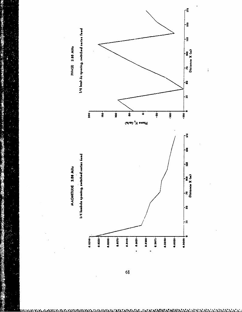
D. THE LPDA WITH COAXIAL ELEMENTS
Many LPDAs have been designed and built over the last thirty years. Whatmakes this research unique is the use of dipoles made of coaxial transmission line. Thecoax dipole was patented in 1984 by Mr. Richard D. Snyder and will be referred to as
the "Snyder dipole' throughout the remainder of this text to differentiate it from theconventional wire dipo!e. The Snyder dipole (Figure 1.4) is constructed using coaxialtransmission line for the inner portions of its segments, connected so that the outerconductor acts as part of the radiator, and the inner and outer conductors of the coax
form compensation stubs. The stubs' impedances vary with frequency in such a way asto cancel the dipole reactance normally exhibited with frequency change, and cAn beconnected in series or parallel. The coax conductors are shorted together at one end ofthe line so that the non-radiating conductor combines with the second conductor toform an impedance modifying stub and the second conductor forms part of theantenna segment (Ref. 51. This leads to a larger operational bandwidth than in theconventional dipole.
If an LPDA using Snyder eilements proves success!'l. ;t wvll have many
advantages in field use over the conventional LPDA, particularly at lower frequencieswith long wavelengths. Advantages include allowing a larger deviation from theoperating frequency, lighter weight, more rugged, and more easily transportable since
the conventional LPDA would require much thicker (and therefore heavier) elements to
11

-. [-'---TRANSMITTER---
Figure 1.4 The Snyder Dipole (from Ref 5).
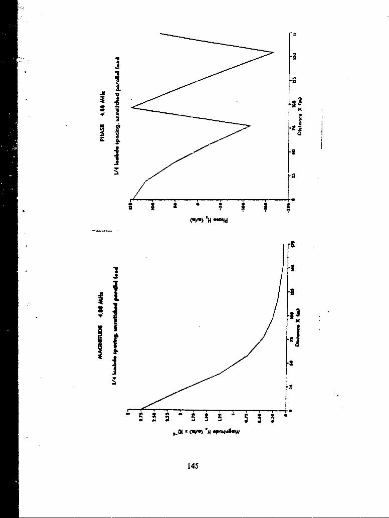
achieve the same bandwidth. Since many of the advantages are size and weight related,
the analysis presented herein will be performed on antenna arrays operating in the high
frequency (HF) band at 3.88 Megahertz (MHz) with a wavelength of 77.3 meters.
12

II. DEVELOPMENT OF THE SNYDER DIPOLE
A. THE NUMERICAL ELECTROMAGNETICS CODE
All antennas in this research were modeled on an IBM main-frame computer
using the Numerical Electromagnetics Code (NEC) version three. NEC was developed
by the Lawrence Livermore Laboratory for the Naval Ocean Systems Center (NOSC).
It is a user-oriented computer code used to analyze antennas or other metal structures
based on the use of numerical solutions of integral equations for currents induced on
the structure by an incident plane wave or a voltage source (Ref 6]. Outputs from
NEC include current and charge density, voltage standing wave ratio (VSWR), nearelectric or magnetic fields, and racliated fields. Single and double precision versions are
available for better accuracy as well as versions that allow for large numbers of
network. or wires.
B. PROCEDURE FOR OBTAINING OPTIMUM SNYDER DIPOLEThe goal for the optimum Snyder dipole was to achieve the widest bandwidth
possible with a VSWR no greater than 2:1 without exceeding size constraints. Sincethe operational bandwidth of a dipole increases as the diameter increases, this effort
was restricted to 0.3 inches in diameter, about the size of standard coaxial transmissioncable, This way the design is consistent with the stated advantages of light weight,
ruggedness, and transportability.
The Snyder dipole was modeled on NEC as a standard dipole with twotransmission lines in parallel to simulate the coax segments of the antenna. The firststep was to model a standard half-wave dipole. It was based on a frequency of 3.88
MHz which has a wavelength of 77.3 meters. The dipole was modeled for free space
propagation with no ground plane and the transmission line segments were modeled as
one-fourth wavelength stubs. Both the dipole and the transmission lines were swept
through a frequency range of 3.5 to 4.2 MHz with a resulting output of adnmttance ateach !'requency. The susceptance (imaginary part of the adrmttarice) for the dipole was
capacitive below resonance and inductive above resonance. The susceptance for the
parallel transmission lines was inductive below resonance and capacitive above
resonance, the opposite of the dipole. The impedance of tbe transmission lines were
then varied until a value was found which provided maximurn cancellation of the
13
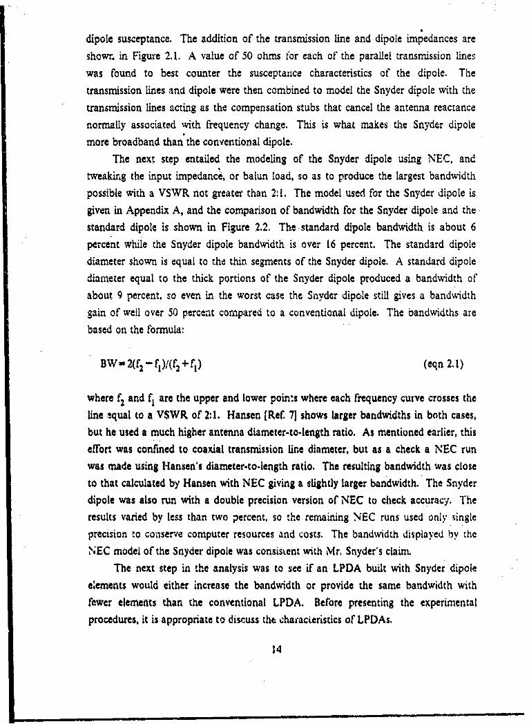
dipole susceptance. The addition of the transmission line and dipole impedances are
showr. in Figure 2.1. A value of 50 ohms for each of the parallel transmission lines
was found to best counter the susceptance characteristics of the dipole. The
transmission lines and dipole were then combined to model the Snyder dipole with the
transmission lines acting as the compensation stubs that cancel the antenna reactance
normally associated with frequency change. This is what makes the Snyder dipole
more broadband than the conventional dipole.
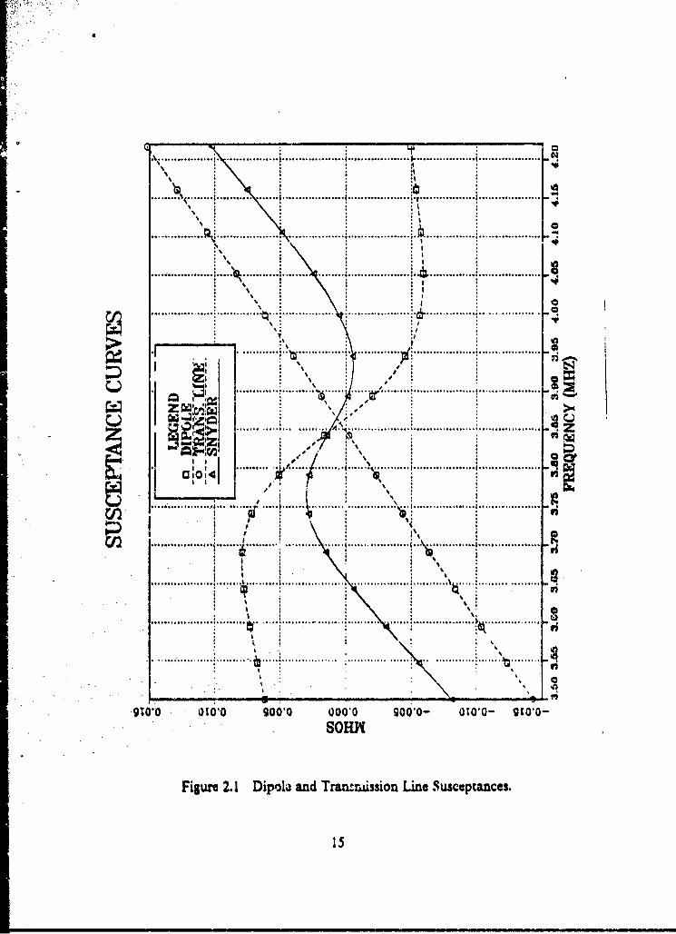
The next step entailed the modeling of the Snyder dipole using NEC, and
tweaking the input impedance, or balun load, so as to produce the largest bandwidth
possible with a VSWR not greater than 2:1. The model used for the Snyder dipole is
given in Appendix A, and the comparison of bandwidth for the Snyder dipole and the
standard dipole is shown in Figure 2.2. The standard dipole bandwidth is about 6
percent while the Snyder dipole bandwidth is over 16 percent. The standard dipole
diameter shown is equal to the thin segments of the Snyder dipole. A standard dipole
diameter equal to the thick portions of the Snyder dipole produced a bandwidth ofabout 9 percent, so even in the worst case the Snyder dipole still gives a bandwidth
gain of well over 50 percent compared to a conventional dipole. The bandwidths are
based on the formula:
BW- 2(f2- f1 V(f2 +f ) (eqn 2.1)
where f, and f, are the upper and lower poin:s where each frequency curve crosses the
line *qual to a VSWR of 2:1. Hansen [Ref. 71 shows larger bandwidths in both cases,
but he used a much higher antenna diameter-to-length ratio. As mentioned earlier, this
effort was confined to coaxial transmission line diameter, but as a check a NEC run
was made using Hansen's diarneter.to.length ratio. The resulting bandwidth was close
to that calculated by Hansen with NEC giving a slightly larger bandwidth. The Snyderdipole was also run with a double precision version of NEC to check accuracy. The
results varied by less than two percent, so the remaining NEC runs used only singleprecision to conserve computer resources and costs. The bandwidth displayed by theNEC model of the Snyder dipole was consistent with Mr. Snyder's claim.
The next step in the analysis was to see if an LPDA built with Snyder dipole
elements would either increase the bandwidth or provide the same bandwidth with
fewer elements than the conventional LPDA. Before presenting the experimentalprocedures, it is appropriate to discuss the characieristics of LPDAs.
14
A .................. ....:• ......... .. •........ h ......... ................... !.. ................ ...................... ........... .................................
.... ,............. ;L ................. ....... ;•..... • "ti...... .... ........ ...... .............. ....................-
.. ........... ........... .i ...... 4. ........ i...... .. ............ . ................ ................... .
. ............. " ............................... ..................
... ... ........... ...
S...... .... i. ... .......... . . . .. -, ............ ..... .. ............. •...................
... . ... .
........... . .... ....
.................. : ........ •... .......... , .......... •...... •..... • .................. ... .. .... ...... ..... .
.......... .. .. .... ......... ...... .........
".IO'0* 10'0 90010 000'0 900'0- 01010- 910o'-
SOHN]Y
Figure 2.1 Dipola and Tramrmi~sion Line Suscoptances.
4 15
....... ....... . . . . .. . . ........
oo.... ... ..... ..oo ...... . . .. ... . ... ...i........... o- -. .o•- - ..... .... .... .-.° ...... ........... ; ........ o .;............
S......:.... ... ! ........ ...... .. ..... .. ........ ...I ........... ........... i........... I ........... .QoS . ............ . .. ....... ... ....... .......... ................ ...............
. . .. . .. . ......•
......... I.. ................t......
.............. ..........
S. ... : . .. i .......... i...... •...... .... i......... .. i........... ........... i........... i............
..Z... ...... ... .. .... ........... . .. .... .. ....
. . . .- : • : : : '. . . . . +
.. .. ...... ........... e.... ... . . ..... ..... ! ..... .. ,,v•l............. ... ..... ...... ........ ... . . . .
Sz.i......i....... I I ...-- '..I..
m + •" z
2-i O's 91T i goWkA
Figure 2.2 Standard Dipole and Snyder Dipole Bandwidth3.
16
llI. lK-BETA DIAGRAMS
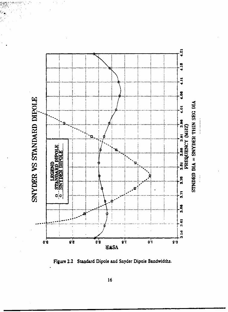
A. K-BETA DIAGRAM DESCRIPTIONOne of the characteristics of an LFDA mentioned in chapter one is that of
backward radiation. It is possible to tell whether or not an array possesses the
capacity for backward radiation by the use of a k-A diagram, also called a dispersion or
Brillouin diagram (Figure 3. 1).
AI d-- 8food side
("ilon 3CFwR)W4S
Sockw.rd. . *_ .wv .
Waves wofel
Slow waves 4~ Slow Waves
0
Figure 3.1 k.0 Diagram (from Ref. 8).
This diagram is obtained by plotting the free space constant k versus thepropagation constant P (or kd versus Pd where d is the antenna element spacing). It is
only necessary to show one period since the log-periodic antenna characteristics repeat
every 2n. For free space propagation:
k- 0 - Itn, (eqn 3.1)
According to Mittra and Jones [Ref. 9: p. 201, the k-I) diagram can be separatedinto three different frequency regions. These are the propagation (P) region, the
complex (C) region, and the radiation (R) region. The propagation region correspondsto the feed excitation region in the antenna and has little or no attenuation. The
17

complex region occurs at 7 t • and acts as a stopband where the attenuation is high
but coupling to space is poor, so the complex region does not facilitate radiation. The
third region, the radiation region, is where an antenna is an efficient radiator. It is also
where fast waves occur, that is, where k is greater than P. The radiation region can be
divided into an Rf region, for forward radiation (away from the feed), and the Rb
region, for backward radiation (towards the feed). Th.- most successful log-periodic
antennas have radiation occurring in the Rb region near the line where 03= - k. The
Rb region should also have a large amount of attenuation to facilitate radiation into
space. It is these characteristics of the k-P diagram that will be used to determine if
the Snyder LPDA has the possibility of producing backward radiation with high
attenuation and becoming a good log-periodic antenna.
B. OBTAINING THE K-BETA DIAGRAM DATA USING NEC
To determine 0, the amplitude and phase of the current along the transmission
feed line can be measured in the near field of the antenna array at different frequencies.
Early experimenters used a current loop placed in the near magnetic field of the
antenna elements and measured actual values for the current phase and amplitude in
relation to a reference point. For this thesis, "experimental data' was gathered by the
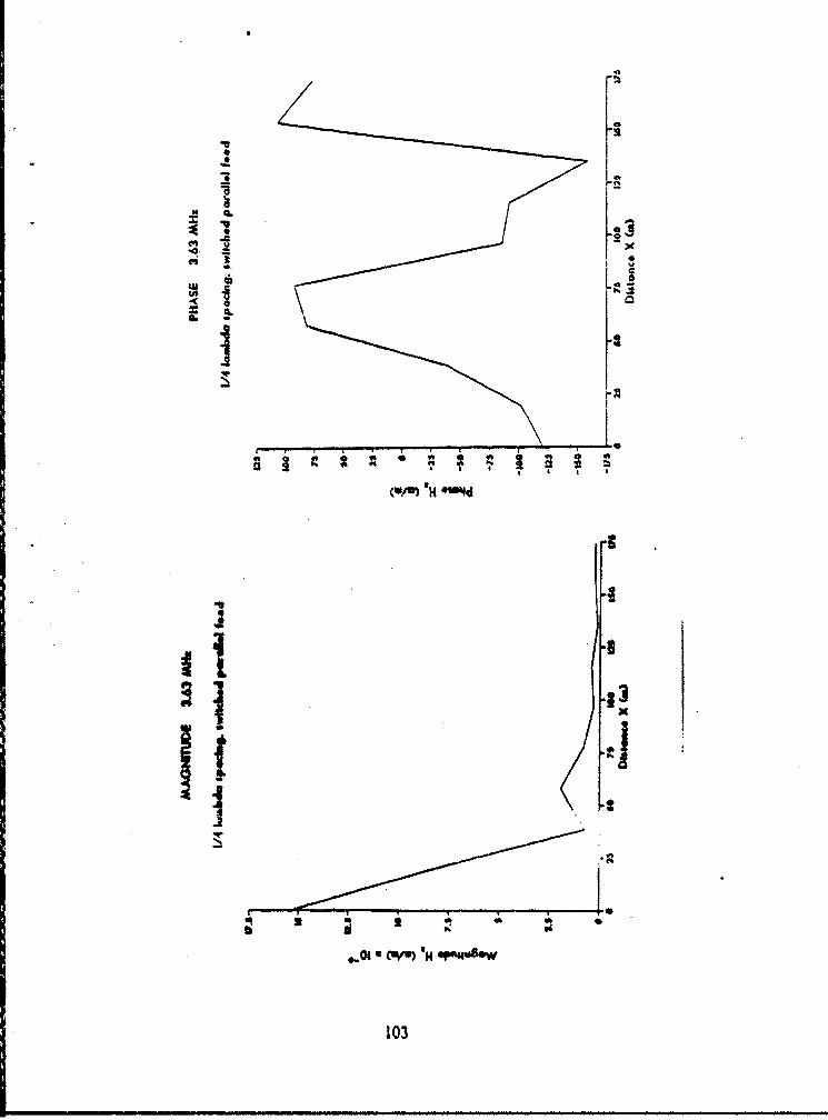
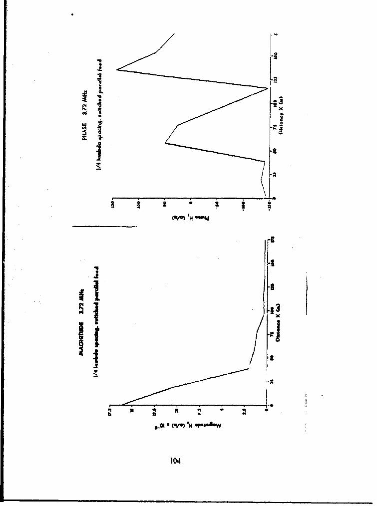
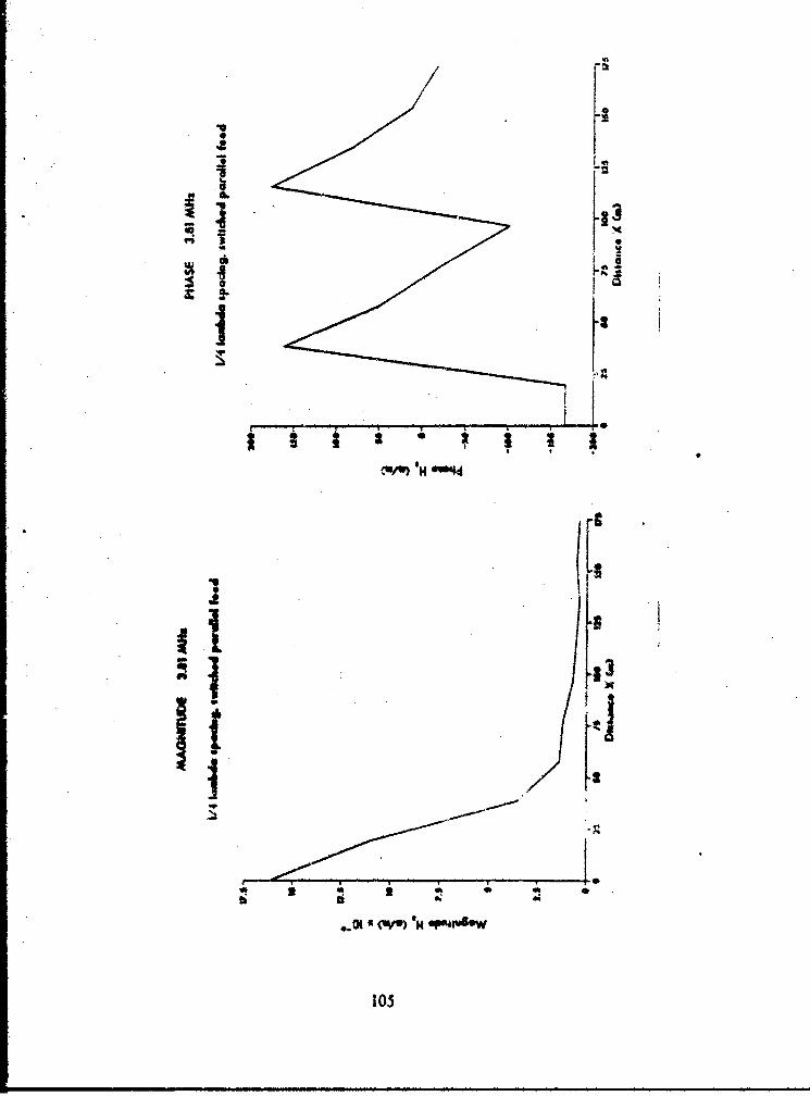
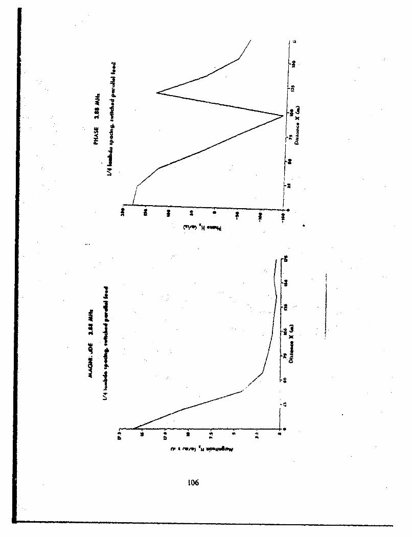
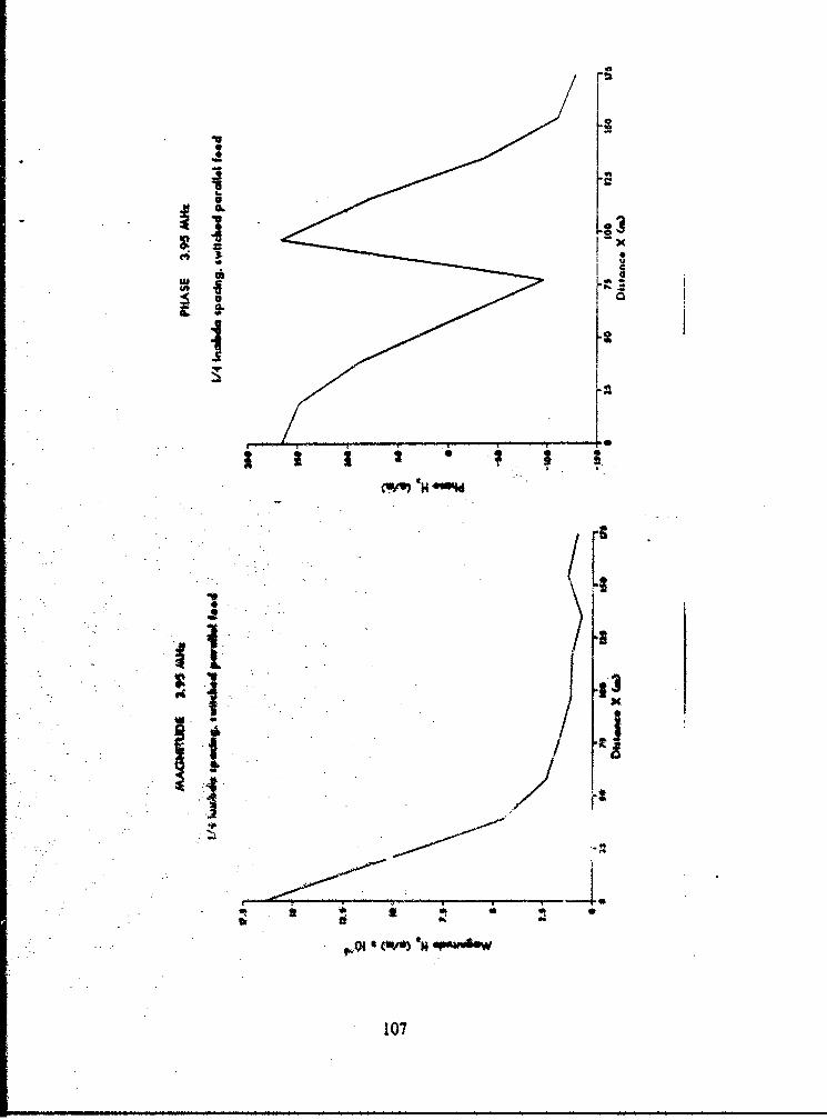
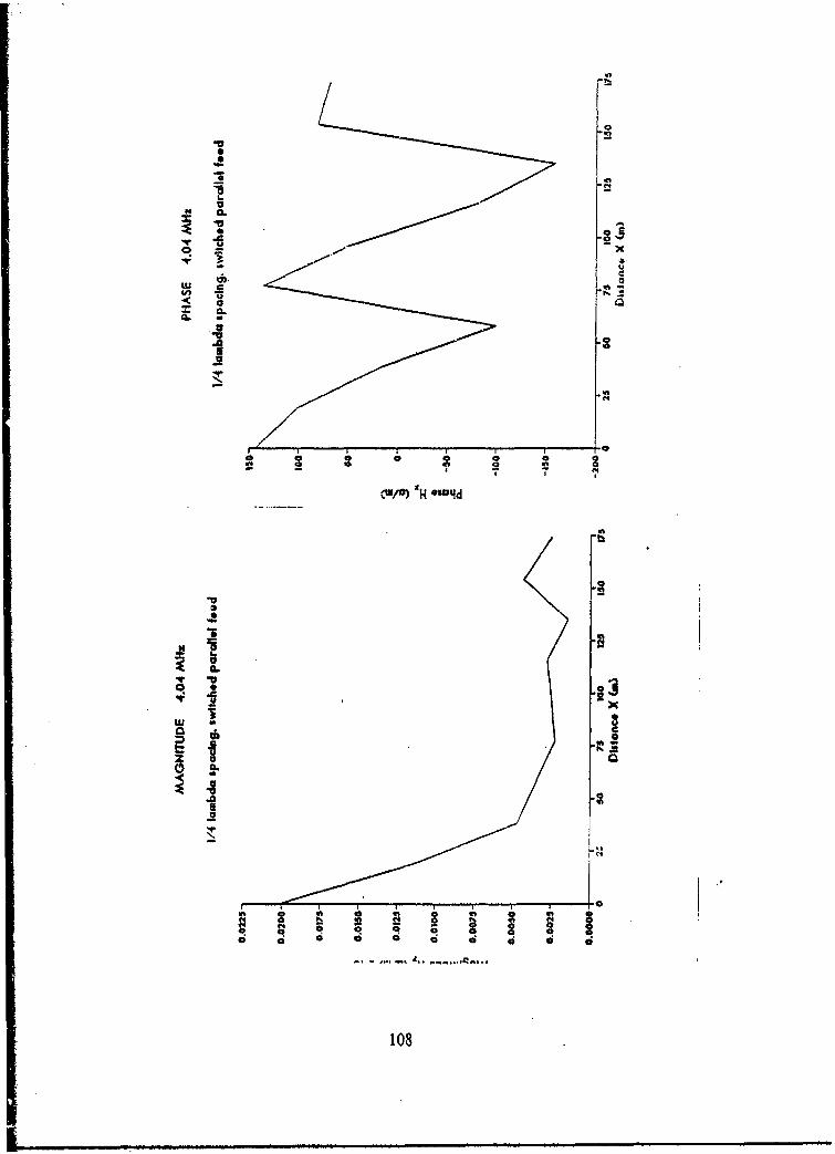
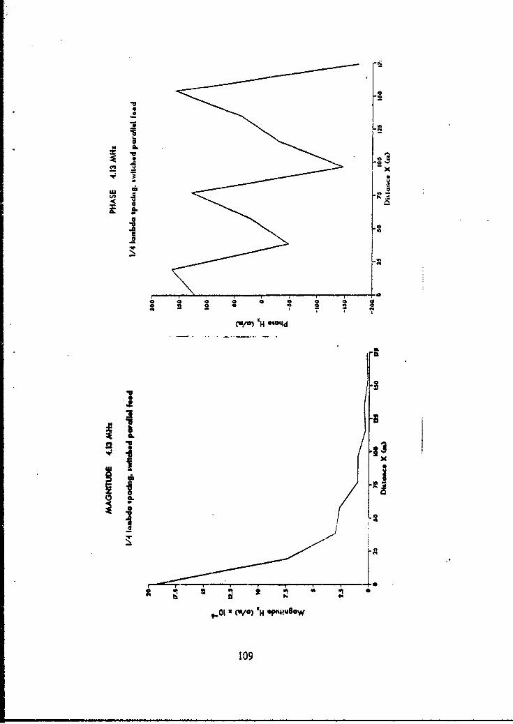
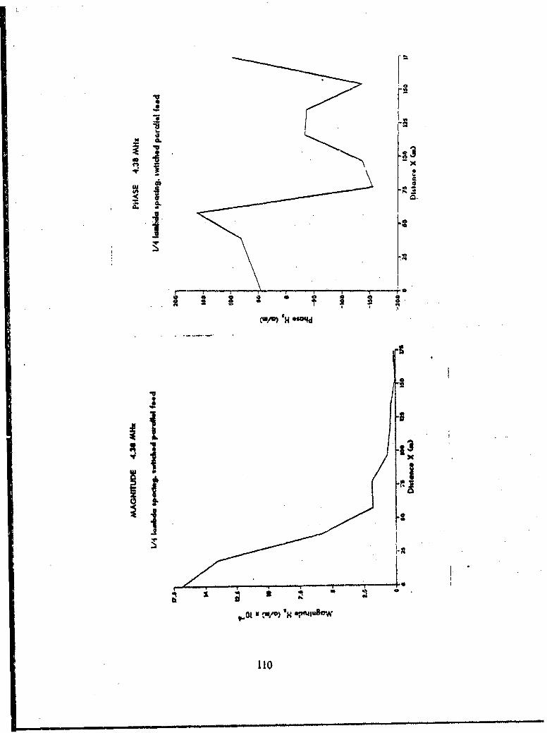
use of NEC to determine the amplitude and phase of the near magnetic fields. The
near field is usually considered to extend to 0.1).. NEC requires near field calculations
be taken at no closer than 0.001X., so several runs were performed taking magnetic field
calculations at distances of 0.002X, and 0.01k.. A comparison of the two distances gave
a magnitude difference of loss than two percent and a phase difference of less than ten
percent. All NEC !nformation used in the final analysis was near field calculations
taken at a distance of 0.01k.
When NEC is programmed for near magnetic fields at one frequency, the output
is the magnitude in amps per meter and the phase in degrees. These values are givenfor the X, Y, and Z directions at each antenna element. The X direction magnetic
fields were used for the analysis since the antenna array was placed in the X-Y plane
with the wave propagating in the X direction. Using a plotting program. the Phase
values were plotied for each type of antenna fied at several different frequenc,.es and
element spacings. The slope of each plot was then multiplied by the element spacing
(d) and converted to radians to produce one point on the k-P (or more specifically, kd-
Pd) diagram. The current magnitude output was used to derive a in the complex
propagation equation:
18
Y-a+jp (eqn 3.2)
These values were plotted using the same plotting program as before. The ratio of
maximum to minimum amplitude was converted to decibels per meter, divided by the
distance over which it varied, and then multiplied by the antenna element spacing to
produce one point on the attenuation plot.
The k-p and attenuation diagrams for the Snyder uniform array are presented
and discussed in the next chapter. By comparing the diagrams of the Snyder array with
those of a conventional array, it will be possible to determine whether or not the
Snyder array shows any ;mprovement over the conventional uniform array.
19
IV. EXPERIMENTAL PROCEDURES AND RESULTS
A. CHARACTERISTICS OF UNTAPERED ARRAYSThe LPDA is made up of elements tapering in length from the longer, low
frequency elements to the shorter, high frequency elements at the feed point. Anuntapered version of the LPDA, called a uniform array, was used to simplify the
modeling necessary for NEC. Mittra and Jones [Ref 9: p. 21] describe the k-0lcharacteristics required of the untapered counterpart of a potentially successful tapered
log-periodic antenna.
Starting from small values of k, the untapered antenna shall have a continuous Pregion, immediately beyond which it moves into an N• region. If the Rb regionis quite efficient (if the coupling to space for the wave in this region is farily (sic)effective), it is immaterial what the k-P properties of the structure are beyond theR region. However, if the P region is interrupted by a C or R1. region ahead ofthe Rb region, the tapered structure derived from it will be a potentiallyunsuccessful broadband antenna. It is therefore quite important to distinguishbetween the C and R regions as previously defined.
It is also important to have high attenuation in the Rb region for proper coupling ofthe wave to space. These guidelines will be applied to the k-P diagrams derived fromthe NEC runs for the various antenna array configurations.
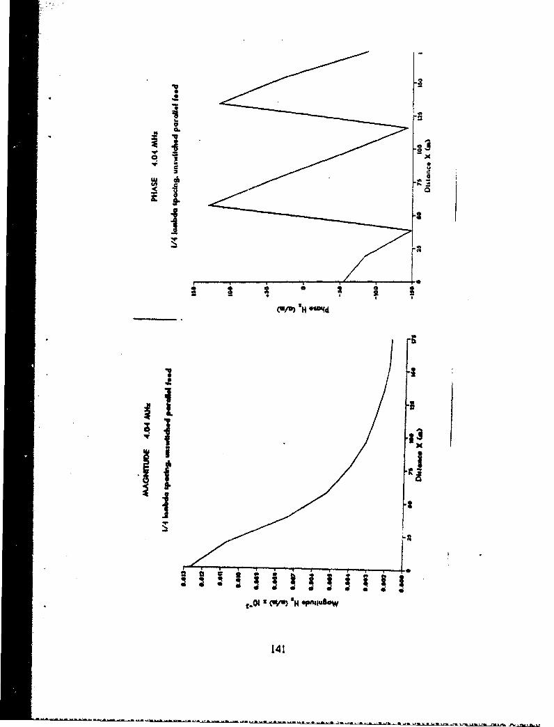
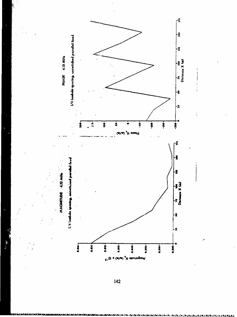
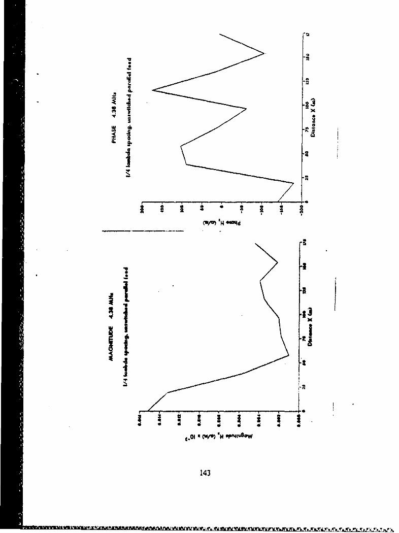
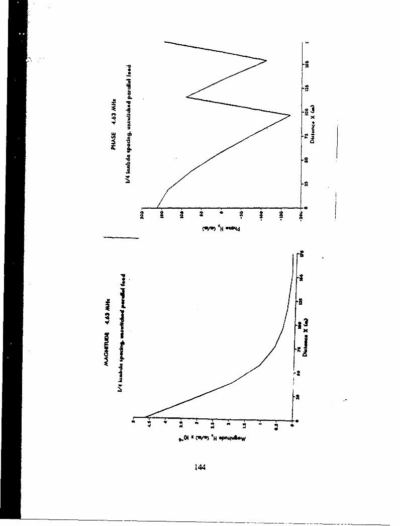
B. DEVELOPMENT OF THE SNYDER LPDAThe antenna modeled as the Snyder uniform array contains 10 elements, each
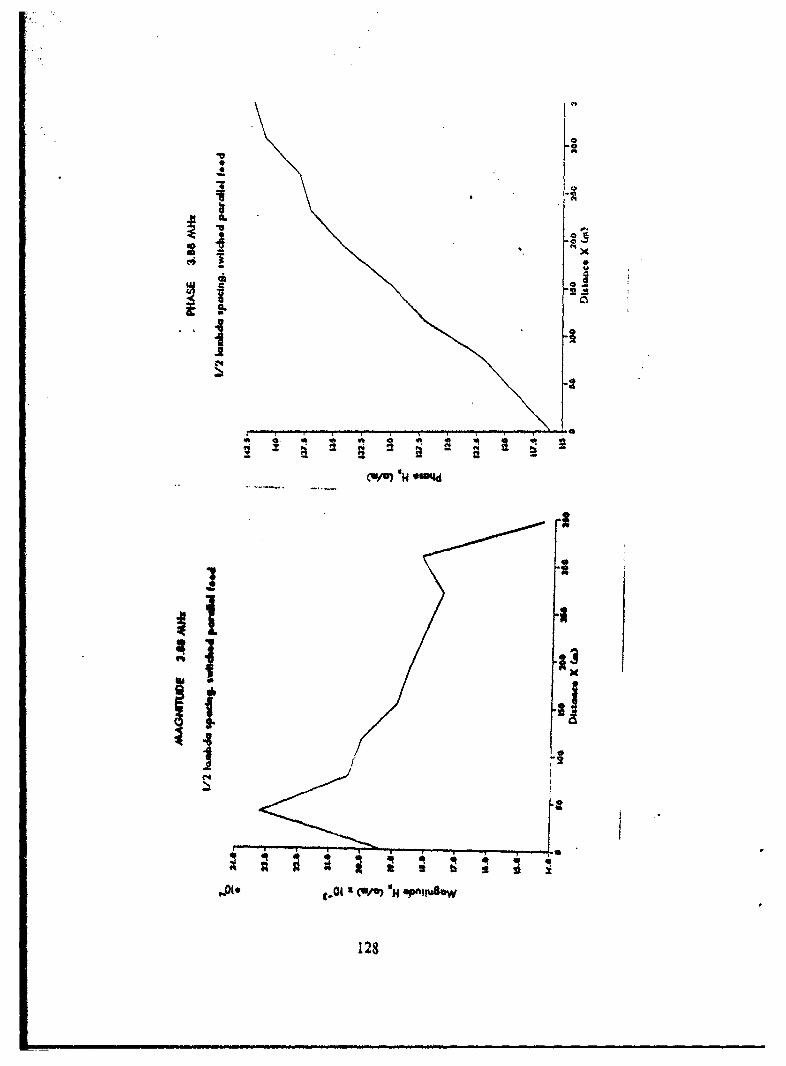
identical to the Snyder dipole (see the NEC code in Appendix A). Each elementconsists of a 1/4 wavelength (at 3.88 MHz) center section and a 1/8 wavelength sectionon each end. The center section is 0.296 inches in diameter and simulates the coaxialtransmission line section of the Snyder dipole by connecting the middle segment to 1/4wavelength stubs, These are the stubs that were described earlier that cancel the dipolereactance in the Snyder dipole. They are opencircuited at the element end and short-circuited at the stub end to produce the desired results. The 1/8 wavelength endsections are 0.144 inches in diameter, barely stretching the NEC requirement thatadjacent wire segments not vary in size by more than two to one. A 300 ohmtransmission line connects each element and the voltage source.
20
The elements were laid horizontally in the X-Y plane with the voltage source P'4
wavelength from the array in the minus X direction, and the 300 ohm transmission line
terminated in a matched impedance 1/4 wavelength from the array in the plus X
direction. The near magnetic fields were calculated in the Z direction at 0.8 meters,
approximately equal to 0.01IX, above the center of each element. The near field values
were calculated for several different frequencies for each array configuration. As
mentioned in the section on k-P diagram data, the plotted values for each frequency
form one point on the k-. and attenuation diagrams. Other sets of k-PJ and
attenuation diagrams were formed by changing the distance between the elements in
the array. If the elements can be spaced further apart in the Snyder LPDA without
losing any bandwidth, then maybe fewer elements would be necessary than in the
conventional LPDA. Different types of voltage feed were also modeled on NEC for
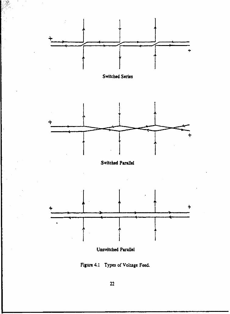
comparison and discussion in the next section (Figure 4.1). The use of the word "feed"
may be a poor choice since it refers to the way the elements are loaded, not the order
in which the voltage is supplied to the elements. All of the antenna configurations
modeled in this thesis receive excitation by means of a coaxial transmission line
running between adjacent elements.
C. EXPERIMENTAL RESULTS
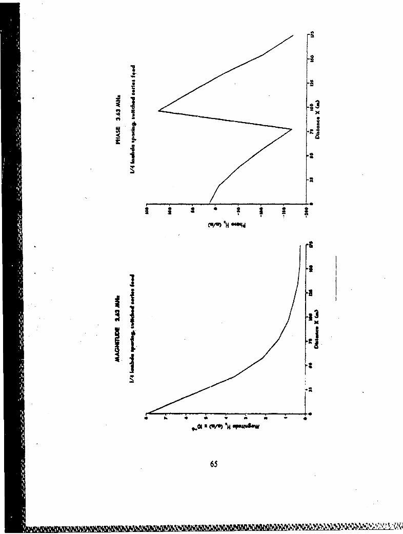
1. Switched Series Army
The switched series feed connects the antenna array elements in series with a180 degree phase shift between each element. This method is not commonly used for
LPDAs, but was tried since suggestions in various conversations led to the idea thatthe switched series feed might produce good results when using Snyder dipole elements.
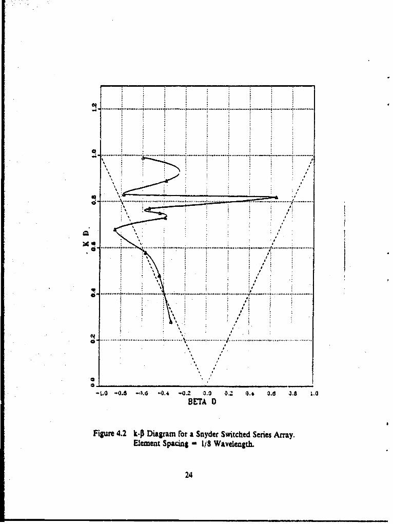
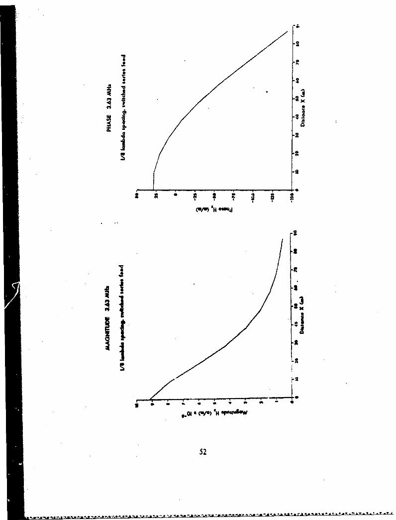
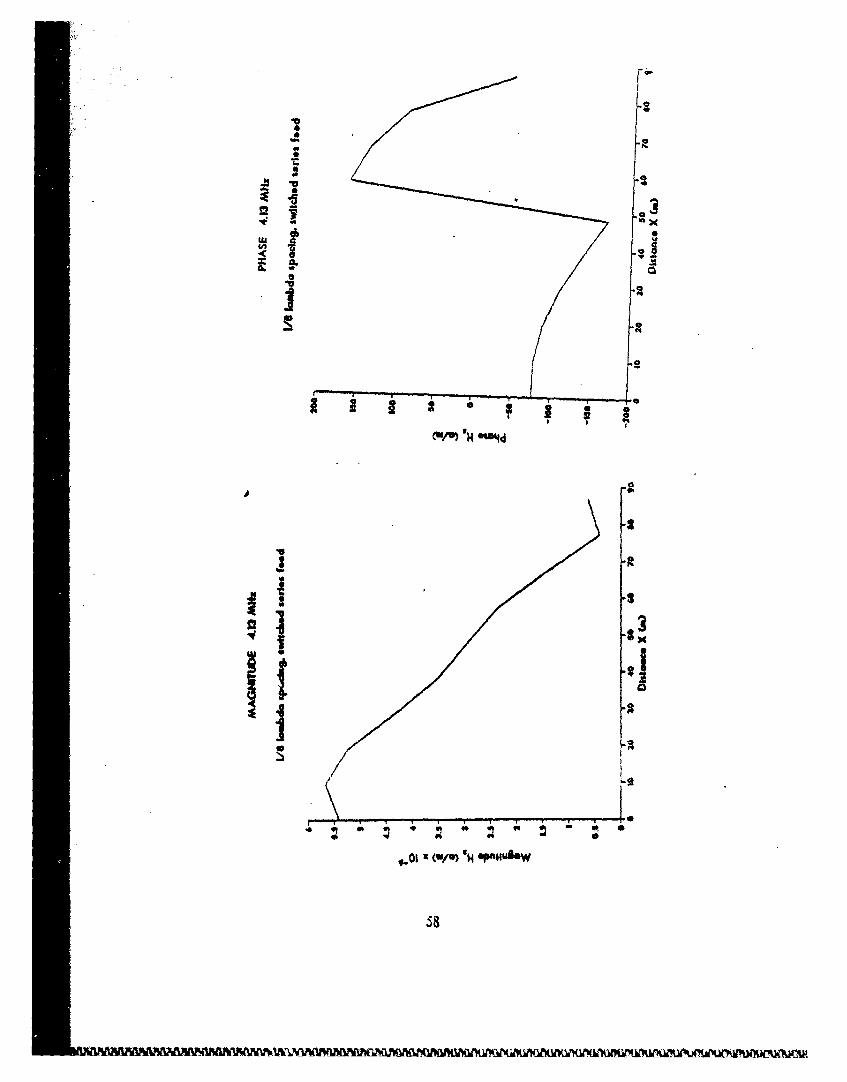
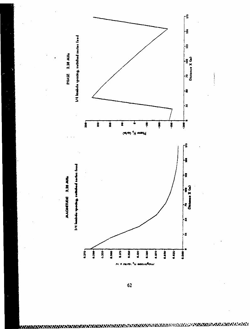
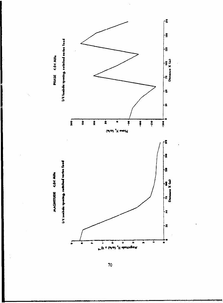
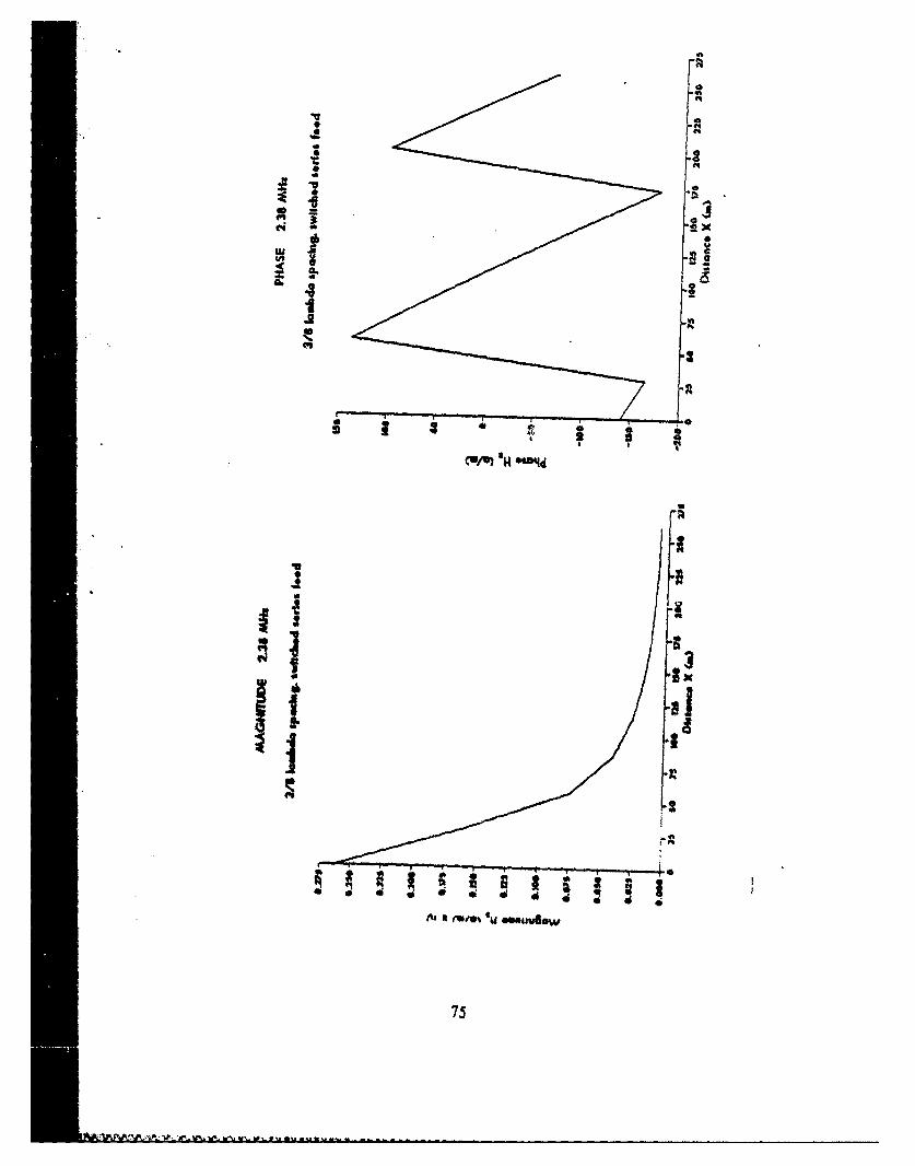
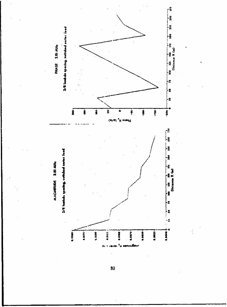
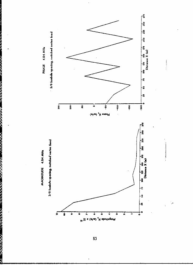
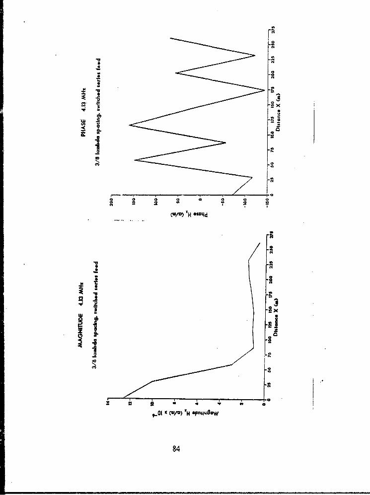
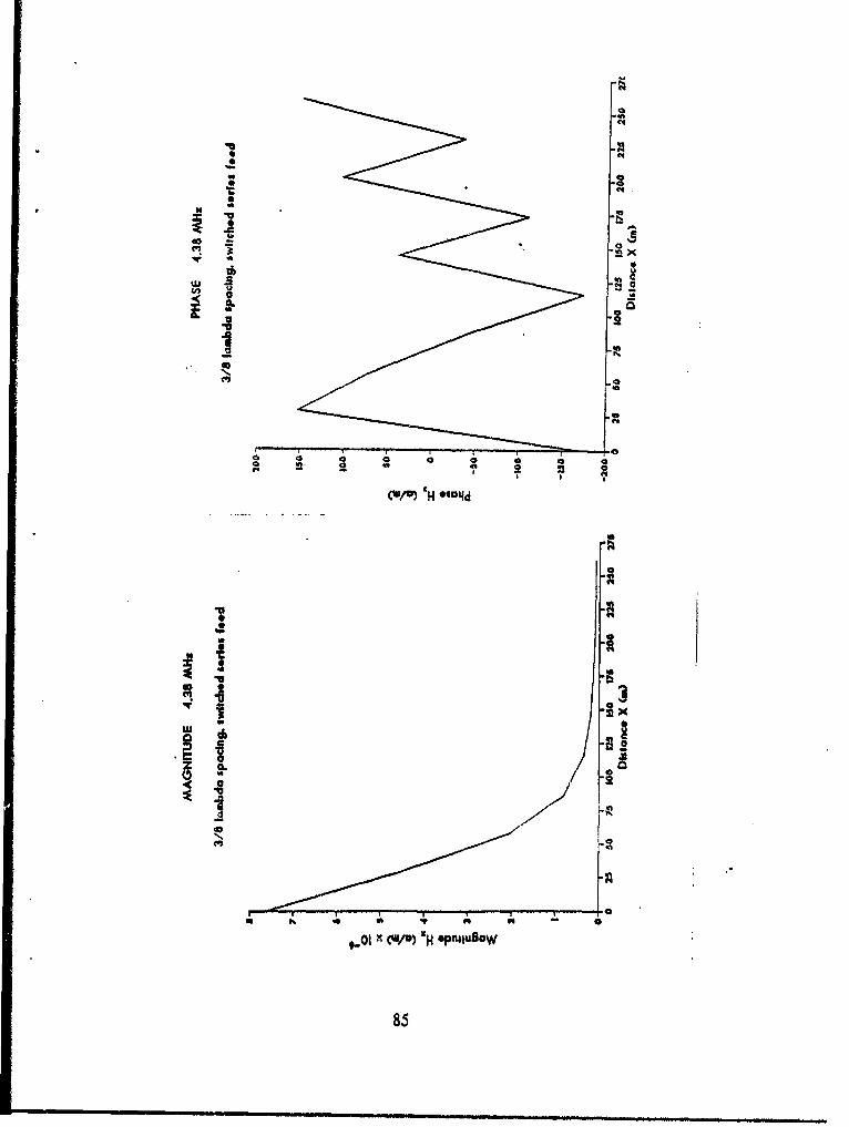
The k-P and attenuation diagrams for a switched seties fed array are presented
in Figures 4.2 and 4.3. The element spacing (d) is 1/8 wavelength for a frequency of3.88 MHz, which is the resonant frequency of the dipole element. All array element
spacings in the remainder of this study will also be in reference to the resonant
frequency of the dipole element. Following the guidelines of the previous section. these
figures show two areas of backward radiation, 3ne extending from the low kd vaiucs up
to 0.77 and the second from 0.82 to high kd values. The kd value of 0.77 corresponds
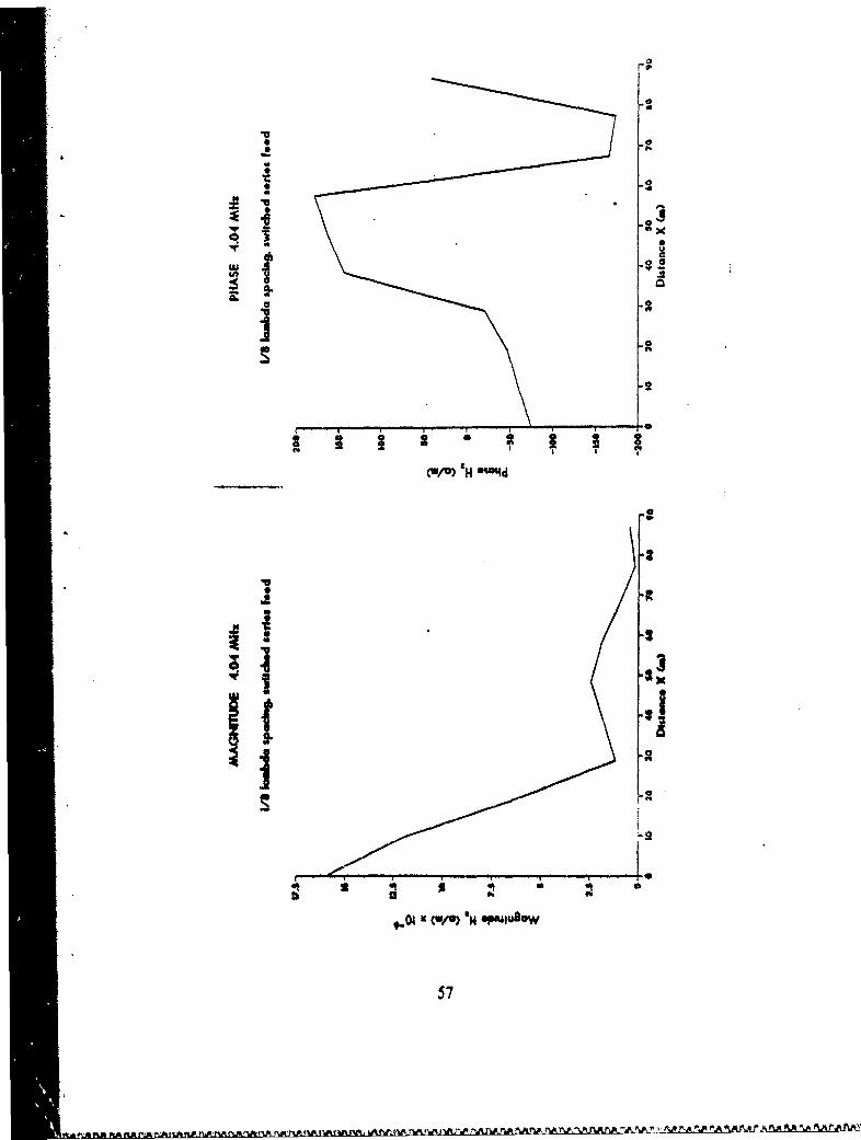
to a frequency of 3.81 MHz and 0.82 equals 4.04 MHz. Even though both of thebackward radiation (Rb) regions are preceded by a propagation region, the attenuation
never goes above 5 decibels (dB), which is not enough to facilitate coupling of the wave
into space. An attenuation of about 15 dB or higher in the Rb region is necessary for
21
Switched Series
Switched Paallel
___1 1 1 +
* IUnswitched Parallel
Figure 4.1 Types of Volage Feed.
22
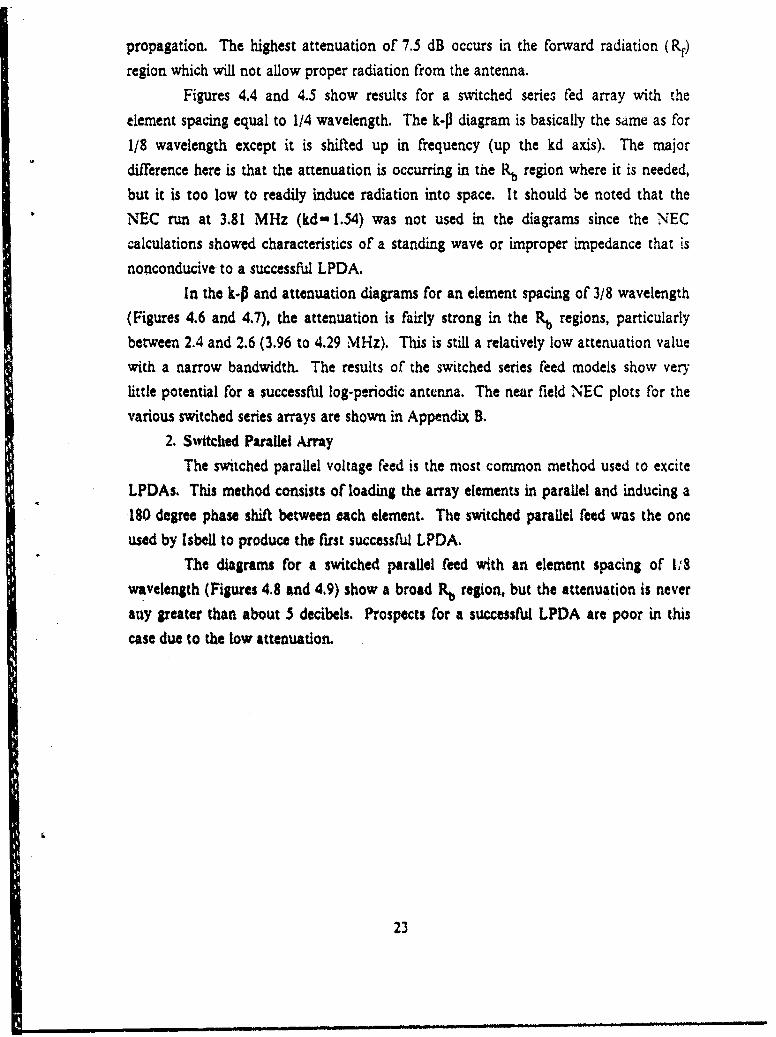
propagation. The highest attenuation of 7.5 dB occurs in the forward radiation (R,)
region which will not allow proper radiation from the antenna.
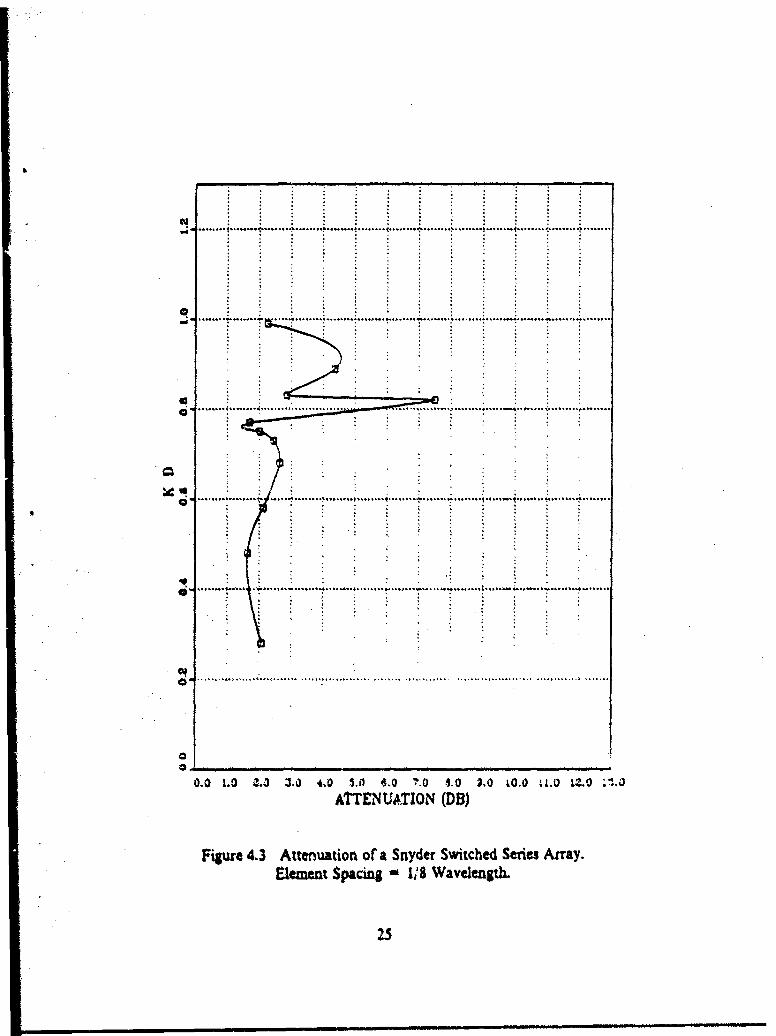
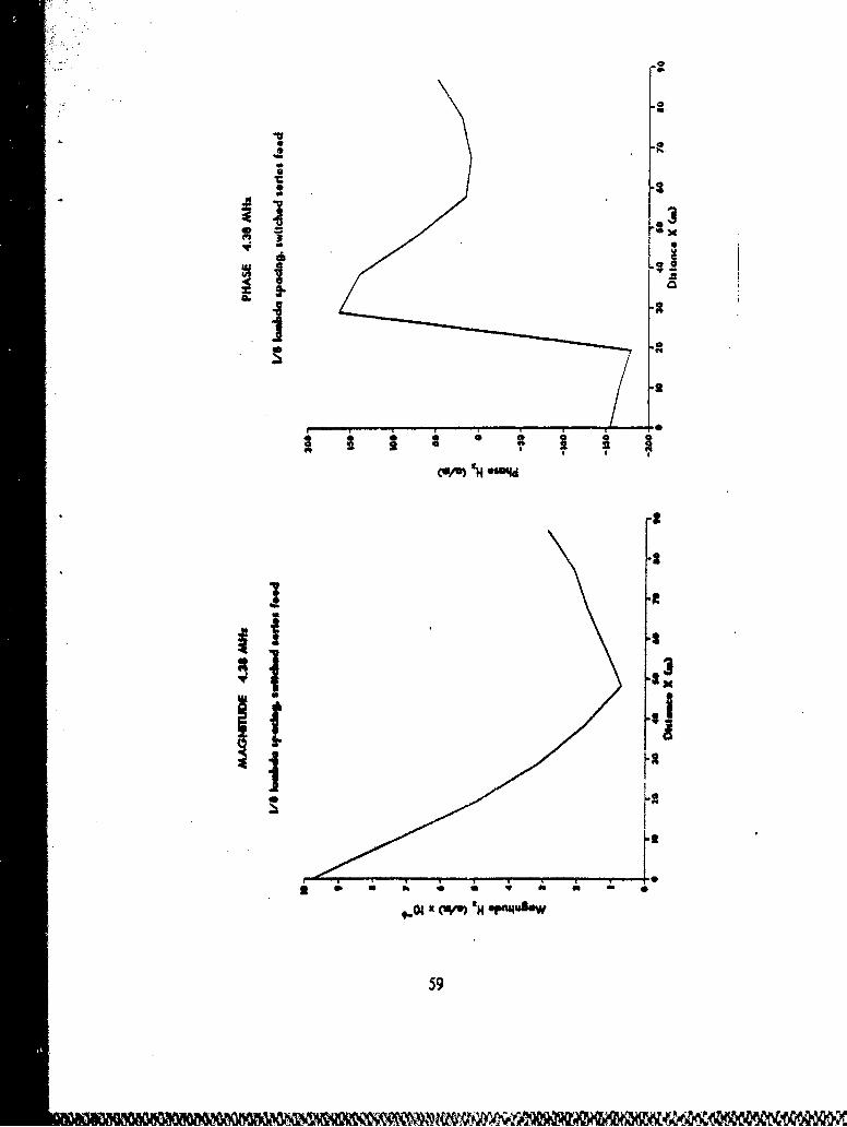
Figures 4.4 and 4.5 show results for a switched series fed array with the
element spacing equal to 1/4 wavelength. The k-fl diagram is basically the same as for
1/8 wavelength except it is shifted up in frequency (up the kd axis). The major
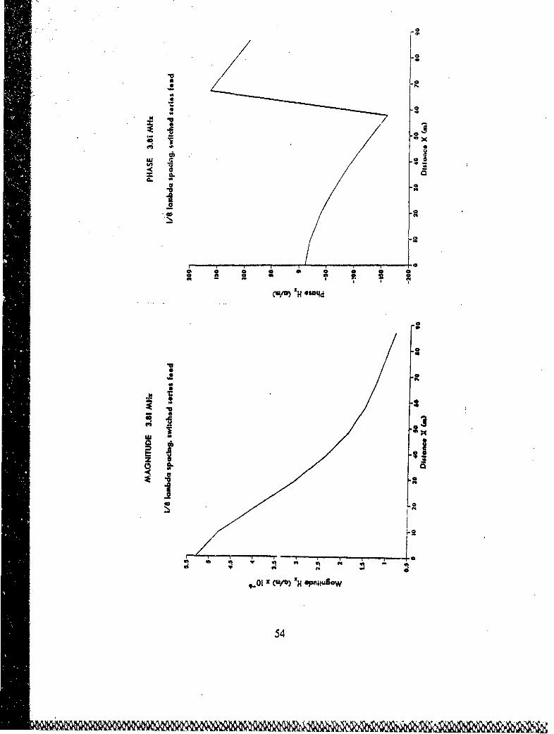
difference here is that the attenuation is occurring in the Rb region where it is needed,
but it is too low to readily induce radiation into space. It should be noted that theNEC run at 3.81 MHz (kd- 1.54) was not used in the diagrams since the NECcalculations showed characteristics of a standing wave or improper impedance that is
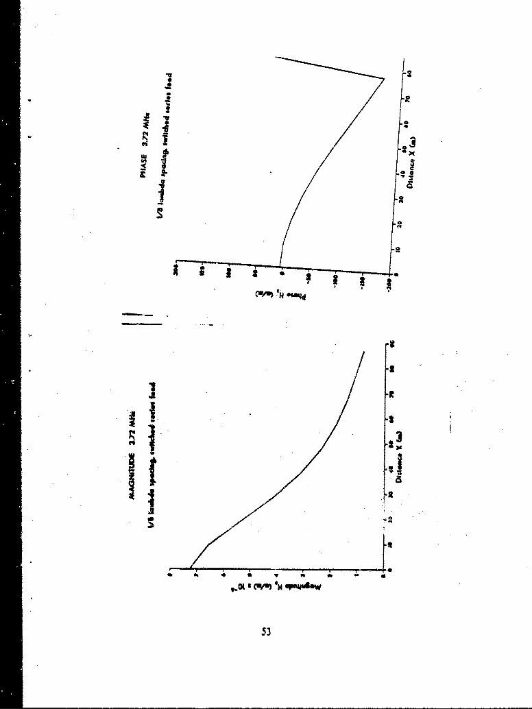
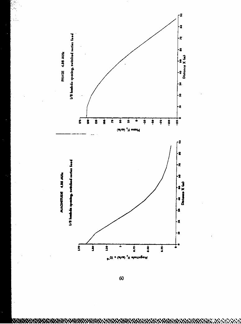
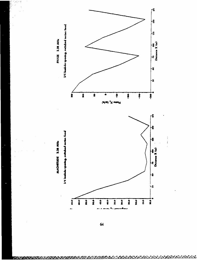
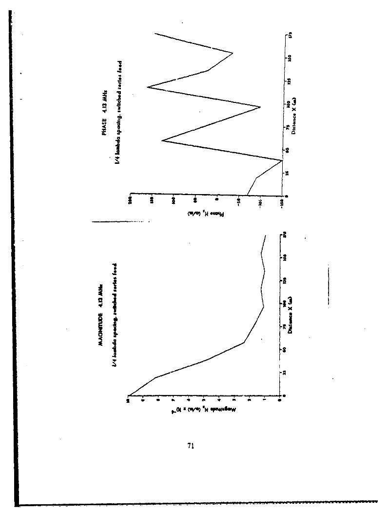
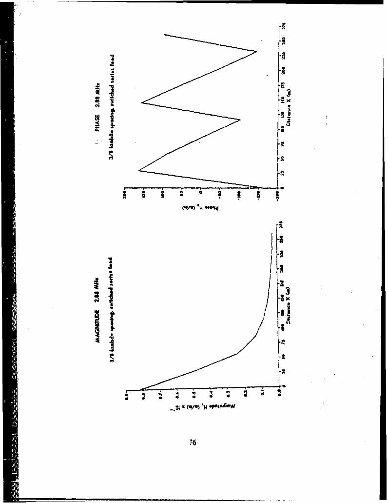
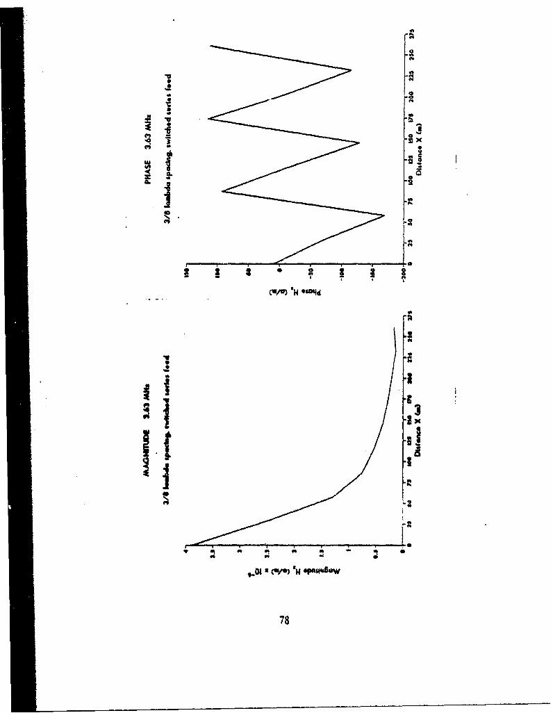
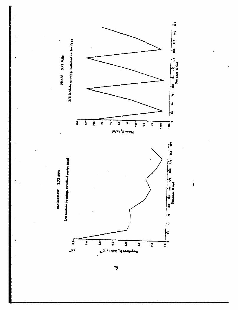
nonconducive to a successful LPDA.In the k-. and attenuation diagrams for an element spacing of 3/8 wavelength
(Figures 4.6 and 4.7), the attenuation is fairly strong in the Rb regions, particularlybetween 2.4 and 2.6 (3.96 to 4.29 MHz). This is still a relatively low attenuation value
with a narrow bandwidth. The results of the switched series feed models show verylittle potential for a successful log-periodic antenna. The near field NEC plots for the
various switched series arrays are shown in Appendix B.2. Switched Parallel Array
The switched parallel voltage feed is the most common method used to excite
LPDAs. This method consists of loading the array elements in parallel and inducing a
180 degree phase shift between each element. The switched parallel feed was the oneused by Isbell to produce the first successfil LPDA.
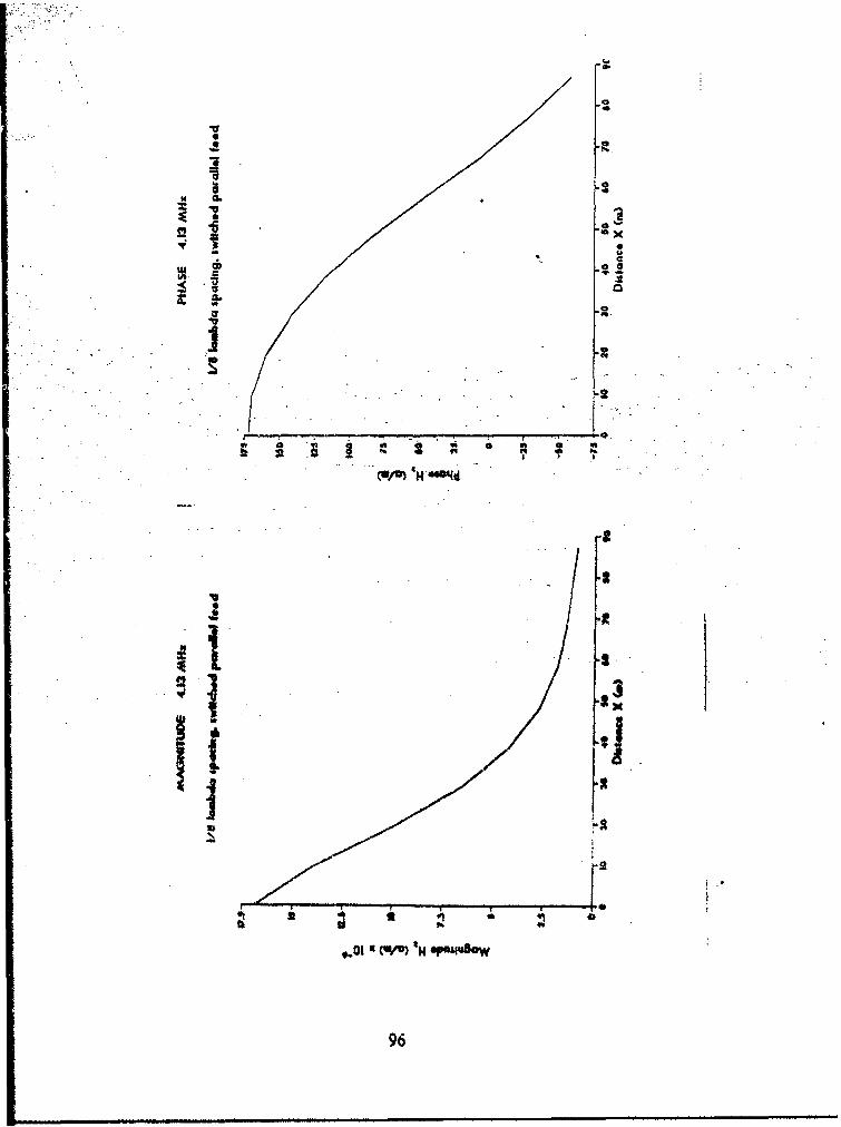
The diagrams for a switched parallel feed with an element spacing of 1:8wavelength (Figures 4.8 and 4.9) show a broad Rb region, but the attenuation is never
any greater than about 5 decibels. Prospects for a successful LPDA are poor in thiscase due to the low attenuation.
23
J_ .. " ** ....... ... . . .
0.. .. .1 .. ...
.. .. ..... ....". .. .......
. ... .... • ..... ... ............... .. .... ... ........ ..... ... ........ -. . . .. .
S I
C
-LO.aO4-4. -. 4-0.2 .JO~ 0 . 04d 3.-6
B ETA D
Fige 4.2 k-Il Diagram for a Snyvde Switched Series Array.Element SPA Ci - 1/8 Wavelegth.
24
m.
. ........ ... .• ........ . ...
.... ..... .. . ...... .... ...
*0.. ..... ...... ... . .... ............. ........ .. .... ..... ..... .. . ........ .. . ......... . . . .
0.0 1.0 2.0 3.0 4.0 5.11 4.0 ý.O 4.0 3.0 10.0 11.0 12.0 .
ATTENUATION (DB)
Figure 4.3 Attenuation of a Snyder Switched Series Array.Element Spacing a 18 Wavelengtd.
25
* I
........... . ............. .... ...... .. ......./.................. .
/0. .. . . ..I. .. ... ...** *` ' .;• • * *... .: . .. . ... ... . .. . ..• ` ` .•... .. .. .. ...` • * ` .* .•.• ......... ,°,......
p.r
... .. .. .... .. .. .... .. .. ...... .. . .. " .... . . . . . . . . ... .. . . . . . . .. . . . . . . .
-24-2.0 -1.8 -1.2 -0.3 -0.4 0.0 0.4 0.8 1.2 1.6 2.0 2.4BETA D
Figure 4.4 Jk.1 Diagram for a Snyder Switched Series Array.Element Spacing - 1/4 Wavelength.
26
iN
70 •
• • . .. ; :: . . . .
.. ........ ....... .. ................e . ..- . .. .. . .. ........... • ....... i ...... . ........................ . . . .. .
...... ... .. ...... ....... ., ....
0.0 1.0 2.0 3.U 4.0 l.(l 4 7. 7.0 8.0 2.0 10.0 11.0 12.0 13.0
ATTENUATION (DO)
Figmue 4.5 Attenuation of a Snyder Switched Series Array.Element Spacing - 1/4 Wavelength.
27
•vo °.o .. o .° ......:........ ..........o°° . .°... .. ~..................... .ooo ..•.° o.°...............°°° .°°•..~o.........
* j
.......... ................ .......... ....
7 ...... ... .................. . .. . ...
................... •......... .......... ,................... •.. ................. •........... ........ ...................
....... ....... ...... ................. I .... ......
. ...........................
. ..... ? . ... ..................... ............. ................. ............... ......... ...................
6 . ................... . . .. . . .................. , ....... . .. ; ............................... •....................* .1
-3.0 -4.5 -P-0 -l.3 -1.0 -0ý5 0.0 0.5 L.0 ,.5 2,0 2.3 3.0BETA D
Figure 4.6 k-lJ Diagram for a Snyder Switched Series Array.Element Spacing• - 3/8 Wavelengtha.
28
IlK N n ii IN I 1 Im I I I III I * I I I •j•"'
a
.. ....... ... ... .. .. .. °.... . °.. . ....... . ..... ... ...
0.0 1.0 2.0 3.0 4.0 5.0 4.0 7.0 ..0 9.0 LO.0 11.0 12.0 13.0
ATTENUATION (DB)
Figure 4.7 Attenuation of a Snyder Switched Series Array.Element Spacing - 3/8 Wavelength.
29
*i i * i, ,, 1111 .
. .. . . . ... *......... .... .... .........
I *
. . . . . ........... ............... ... ......... ........
; t a i
U 30
• *. ...... ..... ,....."","• -- ".... ..... :......... :...~U .Ut .U,..U..,.U..... .... :..... .....
; t , U,
* : ; ; i . ! ! !o . . . . . . . . . . . . . . . . . . . . . . . . . . . . . . . . .. . . . . . . . .
"Eemn Sacn " 1/ Waeegh
; t ' 30

.. .. . . . . ....... ............ ................ ........ ........
. .oo........... ..
... . ... ..... .- ........ .. . . .. .,. ....... ... ....... o...... . ..................
.......... ..... .. . ............. ......... .... ........ ........ ..... ........... ' . . ...
060 L.0 2.0 3.0 4.0 5.0 8.0 7.0 8.0 1?.0 MO. Iu.0 12.0 '13.0,kTTEINUATION (DB)
Figure 4.9 Attenuation of a Snyder Switched Parallel Array.
Element Spacing - 1/8 Wavelength.
31
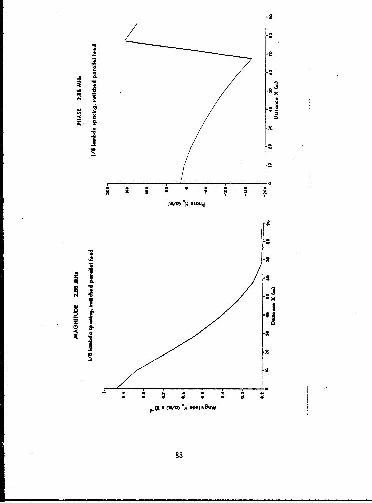
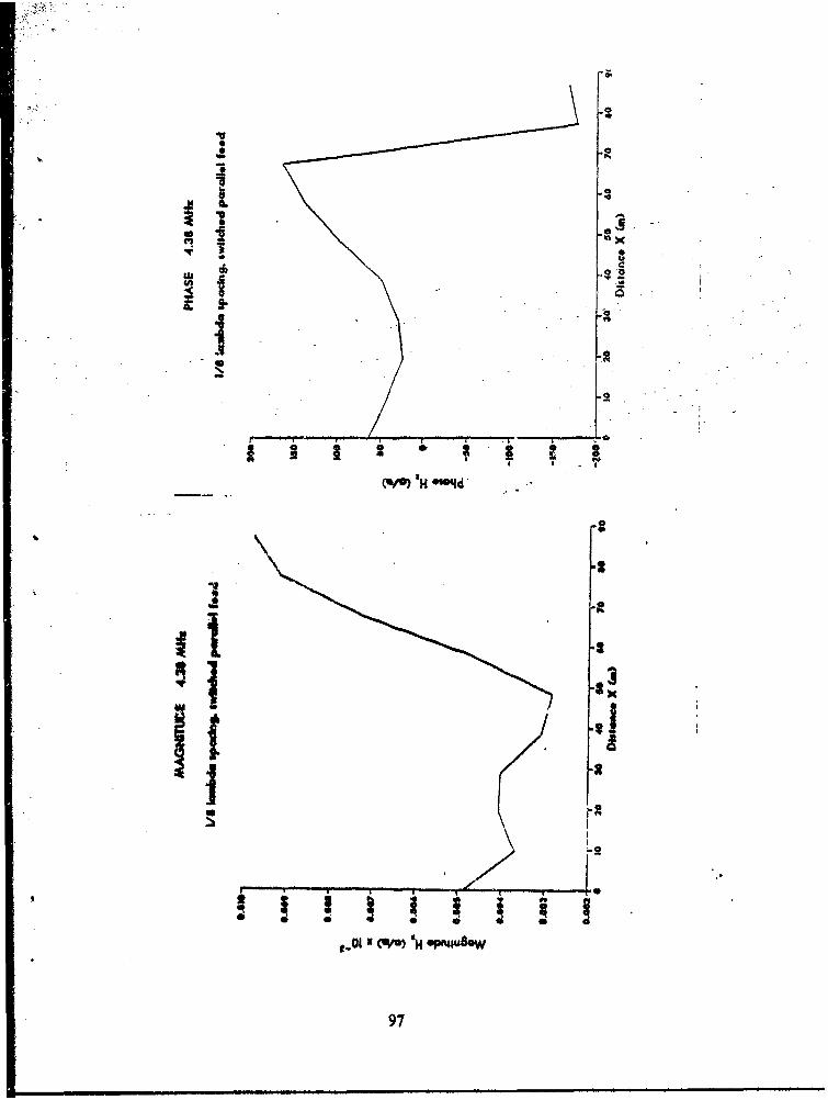
The k-l3 and attenuation diagrams for a 1/4 wavelength element spacing
(Figures 4.10 and 4.11) show much improvement over those of the 1/8 wavelength
spacing. A broad Rb region exists up to kd equal 1.65 (4.10 MHz) with high
attenuation in at least part of that region. This is conducive tu backward radiation, a
key characteristic of successful log-periodic antennas. The second area of highl
attenuation occurs in an Pf region and thus that portion of the frequency baild would
not radiate well.
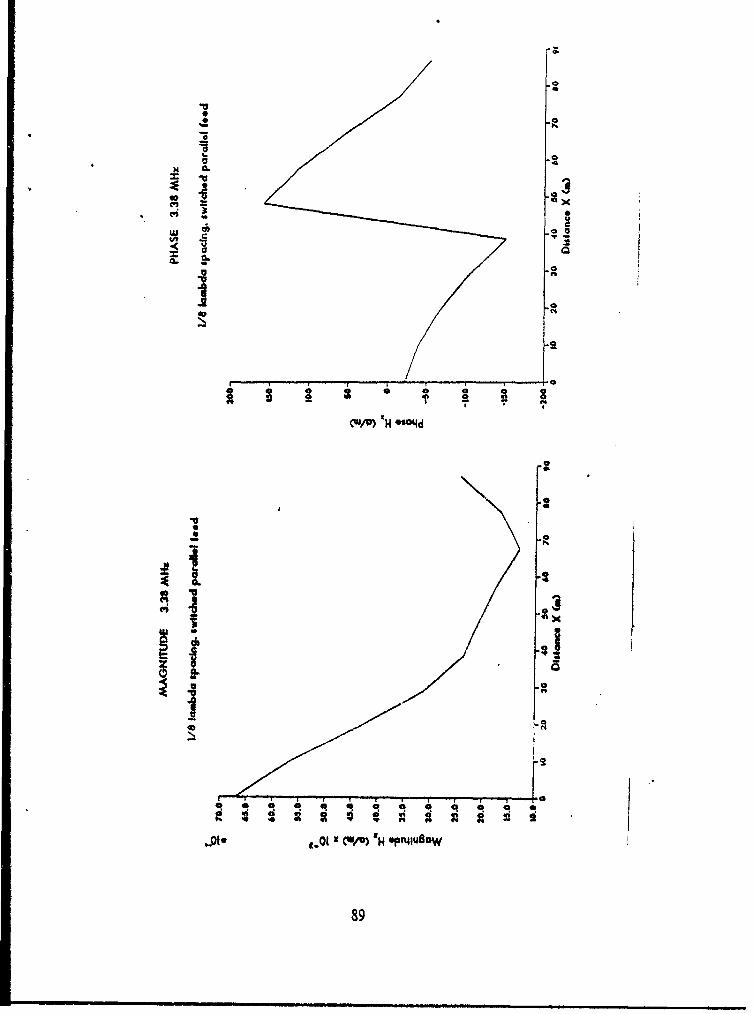
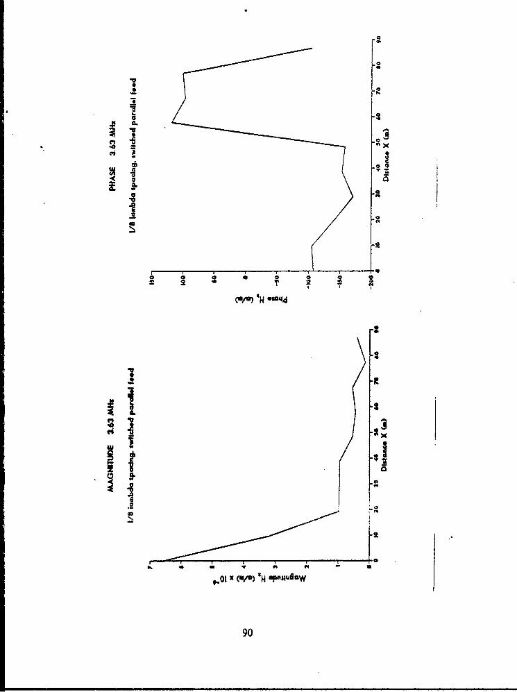
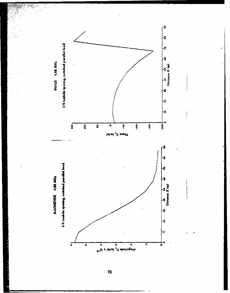
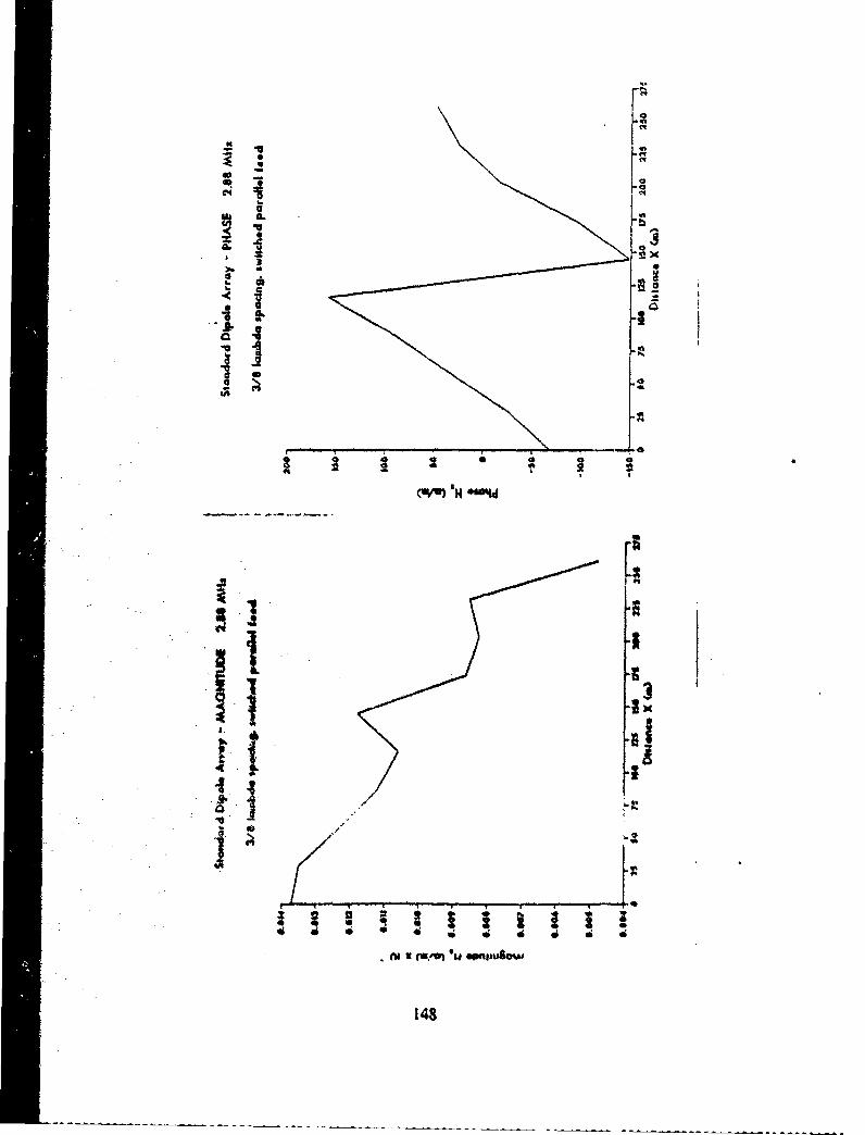
Figures 4.12 and 4.13 show a switched parallel array with the elements spaced
3/8 wavelengths apart. This configuration produced the highest attenuation in an Rb
region indicating good coupling to space, but the backward radiation region is only
from 2.2 to 2.45 which corresponds to 3.63 to 4.04 MHz. This antenna meets the
requirements of being a backward radiator with high attenuation but does not meet the
design goal of having a broad operating frequency.
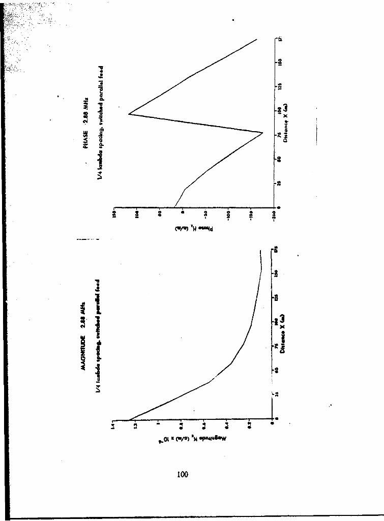
A switched parallel feed NEC run was made with the elements spaced at 1/2wavelength with poor results. Almost every frequency contained characteristics of a
standing wave or imprqper input impedance to the elements. There were no k-1 or
attenuation diagrams produced for this configuration, but plots of the NEC results are
included in Appendix C with the other switched parallel antennas.
3. Unswitched Parallel Array
An unswitched parallel or straight feed configuration at 1/4 wavelength
element spacing (Figures 4.14 and 4.15) did not produce good results, In this case,
there is no phase shift between the elements. Phase shift seems to be a necessary
characteristic of a good log.periodic antenna as Isbell found out when he designed his
farst LPDAs. The k-0 diagram shows a very broad band Rb region but the attenuation
is too low to accomplish radiation. The results in this case were as expected. The near
field plots for this array make up Appendix D.
D. COMPARISON OF SNYDER ARRAY TO CONVENTIONAL ARRAY
The results of the previous section indicate the switched parallel array with 3:'Swavelength element spacing holds the most potential for becoming a successful LPDA.
It produced high attenuation in the Rb region as is required for a log-periodic antenna.
To determine if the design goal of producing more bandwidth than a conventional
LPDA has been met, a uniform array with standard elements was modeled in NEC.
All characteristics were modeled exactly the same as the Snyder dipole except that
32
BC
•1 i i i-i - ,-,, - , *H - bI•ml
* II
...... .... ..... .... ......................... .... ...........:......... .......
V -
.• .......... .......... .. ................ ........ ;. ......... ...... ,............. ......... .I........ ,..........
.1
........... ......................... . ..... t ..... ...........
-2.4 -4O0 -L. -L.2. -0.8 -0.4 0.0 0.4 0.8 1. 1., 2.0 2.4BETA D
Figure 4.10 k-P Diagram for a Snyder Switched Parallel Array.Element Spacing - 1/4 Wavelength.
33
ql
?.....].... ....... T .. .... . .... ........... .............. " ....... It....... .........
•1•~ ~ .......o~~oo~. ...............
0.0 1.0 2.0 3.0 4.0 3.0 8.0 7.0 6.0 9.0 10.0 1L.0 12.0 13.0ATTENUATION (DB)
Figure 4.11 Attenuation of a Snyder Switched Parallel Array.Element Spacing - 1/4 Wavelength.
34
.......... m m mmm m m m wm • m m m ml lm ul l l - •..
.. . . . . .. . . . . . .. . . . . . .. . . . . . . . . . . . . I
.I
I ................ .... ........................................................... "._ : "... ........... ....................
• " ~ ~ ~ ~ ..... ...............................°"°°'° *'" :'" "°" ... ...... ........................-*°'°'"
.. ...... .... •....... :........ .V,..\. ....... •........:........•............... .................. ...... *.............I
"". , ; I * *
4d ....... i..... • ....... •....... . ........... ............... ................. -....... ....... ................
-3.0-2.5 -?.2 -1.8 -L.4 -L.0O-0.6 -- 2. U.2 0.6 1.0 1.4 L,.8 Z-6•. 3.0
BETA D
Figure 4.12 k-P Diagram for a Snyder Switched Parallel Array.Element Spacing - 3,18 Wavelength.
35
.°.., . .,~ ...°° , .. °.°. °... .°.• ° ..... .. ... .... .. . ° ° o ..... ... °. °o•o °. •°.. ° ,. .... °4.....
...... .... .... ... ... ........ ? ..........
6 a 9 OL 4 3 4I e1 is
A U :
u 4
m S
:36
01
o L. ! 3 4 5 * 7 5 9 10 11 iZ 13 14 15 18 17 18ATTENUATION (DB)
Figure 4.13 Attenuation of" a Snyder Switched Parallel Array.Element Spacing - 3/8 Wavelength.
36

..... ... ......... ......... •........... ......... ......... ......... •........... ........ . ......... •.......... .........
......... ..... . ............ .......... . ..... ...........
0'- , - . - . - - . - - -
... . . . .. ...
S........ ......... ......... .................... • .... ............. ; ................... ;.......................... ..
* . , .I .
-. -i,0i. 3 -0 , 4 0. 0. 0. t.2i 1. Z -0, 2. -4-
Figure- 4.14 k-P Diagram for a Snyder Unswitched Paralll Array.Element Spacing - 1/4 Wavelength.
37
Seg• inn ~~~~*Id ilMIm i f ~ildi ilbaqlMid~a~ i I~d
.......... I ........ ......... ........ ................. ......... T ....... ................ ................... ........
.: .................. ......... i .. ......i........ ....... T....... .i ........ i........ ........ ........ ...... .
S....... . ....
............... ..... . . . ..............
.. . . . . . . .. . .. . . .. . .. .. . .
ATTENUATION (DB)
Figure 4.15 Attenuation of a Snyder Unswitched Parallel Array.Elesnent Spacing - 1/4 Wavelength.
38
there are no coaxial transmission line sections and the input impedance to each
element is 73 ohms, the same as that used in the standard dipole in chapter two. The
same values were used for the physical dimensions, element spacing, transmission feed
lines, voltage excitation, near field measurements, and frequencies.
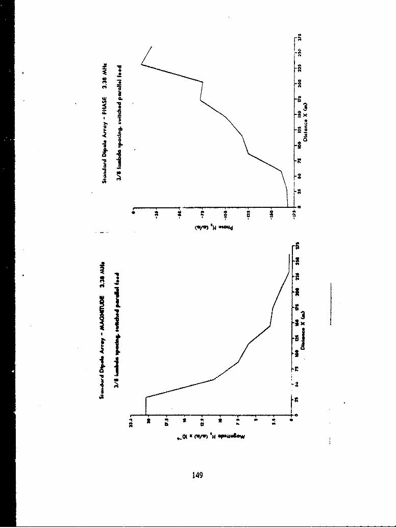
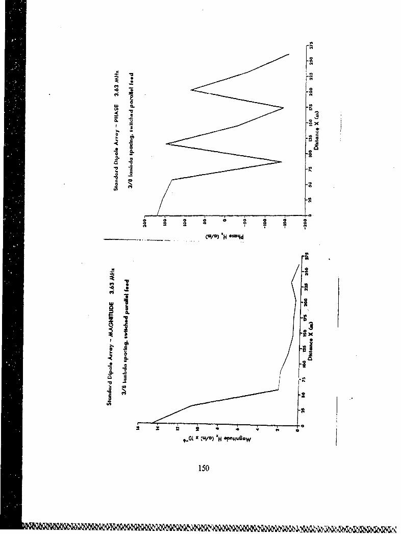
The resulting k-13 diagrams for the conventional array are Figures 4.16 and 4.17.
"These diagrams show very similar results as those for the 3/8 wavelength Snyder array
(Figures 4.12 and 4.13). The Rb and Rf regions are about the same in both cases, as
are the attenuation curves. The highest attenuation in both cases is about 17.5
decibels in the R. region. The frequency bands of the R-b regions are almost identical
so that there appears to be no bandwidth gain in the Snyder array. A direct
comparison of the two arrays is presented as Figures 4. 18 and 4.19.
A standard dipole array with 1/2 wavelength element spacing was also modeled
with NEC, but the results were as poor as the 142 wavelength Snyder switched parallel
array. The near field plots for the 3/8 and 112 wavelength standard dipole arrays are
included as Appendix E.
39
..
.......o.... ......... *....... .....
A D1
Elmn Sain - 3/ aeegh
040
-3. -,0 -24-. 1 0800 0. . € . . .
•o ..... ..... ..... :...................... ..BETA .......... ..... D....
Fiur 4.6kJ iga o Stndr ,w e Paale Aray
ElmetSpcig- / Wavelngth
• t: : " .40
'I t
... .... ..... .. .... .... .. .. ... . .
o 1 2 3 4 7 8 9 1 1± 12 13 L4 15 LO8 L7 L8ATTENUATION' (DB)
Figure 4.1i7 Attenuation of a Standard Switched Parallel Array,Element Spacing - 3/8 Wave-length.
41

/0
4.
LEGENDK =MINUS BETAK '= ET
-3.0-.0 -L4a -1.8 -1.8 -Q-6 0.0 0.0 1.2 1.8 P.6 3.0 3.8BETA D)
Figure 4.8 k-J3 Diagram Comparison.
42
0..
0 . . . ....... .
o .4
! .. .. . .. . . . .
l l!~~~~ ~ ~........ .... ...... ......+ .. ...+ + ++ +................... ..... ......LEGENDSSTANQ6ARIn ARRAY
a 6 7 a 9 t0 i t 1i 13 14 15 18 17 toATTENUATION (DB)
Figure 4.19 Attenuation Comparison.
43
V. CONCLUSIONS AND RECOMMENDATIONS
This thesis examined the feasibility of designing a log-periodic dipole array with
more operational bandwidth per element than the LPDAs currently in use. Toaccomplish this, a Snyder dipole made of coaxial transmission line was modeled using
the Numerical Electromagnetics Code (NEC). It was then placed in a uniform arrayand diflbrent configurations were tried by varying the type of feed and the element
spacing. The performance of each antenna was then based on the k-J3 and attenuationdiagrams created from the NEC output.
The first conclusion one can draw from the NEC results. is that a Snyder dipolecan be designed and built with an operational bandwidth greater than that of a
standard dipole. This greater bandwidth will then allow a larger deviation in theoperating frequency without serious degradation of the impedance match. Anotheradvantage of the Snyder dipole is that it achieves the same bandwidth a. a standard.dipole of larger diameter, and therefore reduces the weight.
The second conclusion drawn from the research is that the NEC model for theSnyder dipole is accurate since the results are consistent with the designer's claims andother antenna models. Since nothing was found in the literature to reference on theuse of coaxial transmission Line elements in uniform arrays, it is assumed the NEC
model for the array is also accurate. The k-P and attenuation diagrams showed thatbackward radiation was produced at some frequency for every kind of feed and element
spacing used, but the attenuation was often so low that no radiation from the antenna
could occur. For the case where there was high attenuation, the bandwidth was nobetter than that of a standard array of the same element spacing. This leads to thefinal conclusion; the Snyder dipole does not improve the bandwidth of a conventional
uniform array.The results of the Snyder uniform array data are disappointing, but before
completely disregarding the Snyder dipole as an LPDA element, it is recommended that
the effort of this study be continued by modeling a uniform array over various grounds
to see if there is any advantage in using the Snyder dipole in that situation. It is alsorecommended that a Snyder LPDA be modeled on NEC. This study showed that the
Snyder uniform array performed no better than a standard uniform array, but the
44
characteristics of the mutual impedance of the Snyder LPDA elements may prove
advantageous in a tapered array. Modeling a Snyder LPDA may require a new set of
design nomograms based on input impedance since the nomograms currently used for
standard LPDAs may not be applicable. If the same conclusions are reached as those
from this research, the Snyder dipole array should be removed from consideration as a
potentially successful LPDA.
It should be noted that even though the Snyder dipole failed as a uniform array,
it did produce excellent results as a single dipole. The Snyder dipole should be
considered for any use where an increased dipole bandwidth is desired or necessary,
particularly if coaxial transmission cable can be used to maximize the performance.
45
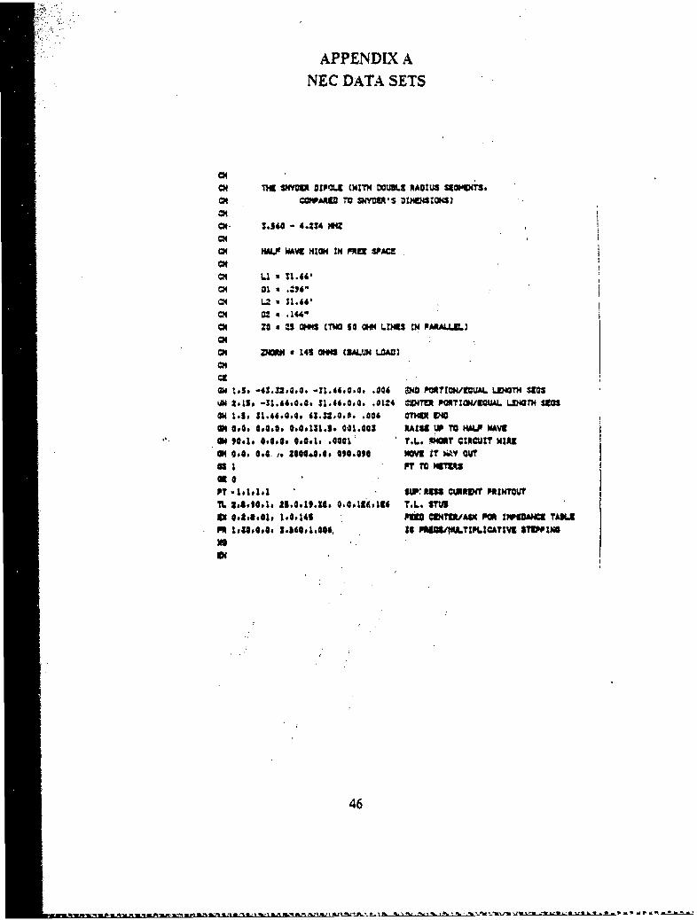
APPENDIX ANEC DATA SETS
c"c S'm D O tOlE C1mmTn Oumu RAOMUS stmeW4i,c 04t O ItO TO UNY=-S DIIV4,iON
cmcm- :.So - 4.2S4 MW
cmcm 14ALFWAVE HIGH INR IU SPACEcm
cm Ol 2 l.:96*
cm ,t a31.66'
ch ZO :3 0" (1' SO LfldIS 0N LIM 94 ,IL)cmcO x OM a 145 ONO CUMLN LUC)cmcgOW 1&3# -4342.0.0. -11.466040, .06 ýHO P• 'tNGNOH UAL. WL4OTN $103ON loll# -31.64.0.4. 11.46.,44. .0124 MTNT O"T?0d/5CUIL LVmOITH Sm0OW ls1 S1.66.40.4. is6.340,0. .006 QTMl[S V40
04 0.0$ 0.0,0. 40.0131.5., @41.003 RAISE S TO NN.P WAVC"ON 90.1s. 0.60. 00*Aft .0001 ?.1.. t•OT CICWUT MiWAeam 0.0. 0.C. if 200104.40 00.00 "m iT 4v CVt
03I P? m UTRS
Py "1.1.1.1 5.UIR, AUS c'to¢ PIl WTL. 2.5.10.l. 23.90.14s. 0,0.11'•6*146 T.L. flUIIX 00,2000•1 1,0.141 P W4T31AVC PM IWIDMG TAIMEPR 1#.18.0.0 S1.6001.004, S0 II1ftOSLTPL3CATSVI STUPtMN
S46
+.4

C.'4 UNIFORM :NYCER 0:P01. ARRAY
CM (SWITCHED SERIES FUD-JD
cM
C4 DIPOLE: LENGTHe 1/4 I.DAI41A AT FRED. 3.38 MMZ
'14 rZOMEN'T I.E-NG-.HSs .11.66 FT
LM THIN OIAMeT~q- 3.1644' 3..10183 METER R~ADIUS
C~m THICK D3IAIETVR* 3.1.76" 0.00376 4M TR ADIUS
C.14
Cm 10 M.".EN4T ARRAY
Cm ~ E-LEIMENT EPAC:.NG - 1/8 'dAVEL.E-NGT14 (29.93 ME&E S3
Cm
-4 ~ ~ o :sx 2S s OHM C:O 50 OHM L ZE N PARALLEL, OR
Cm 12.5 SEZIDE 12.5 :M PARALLE.L.]
Cm Z-NORM v 165 CHMS (3ALUM LOAD)
CM Z-FEEfl LINES - $00 OHMS
Cm
Gw 10.5. 0.-19.30.02 0.-9.65.0, 0.00183 FIRST ."4IN sEG'mer
G14 20.16. 3.-9.6S.J. 0.9.6S.0. 0.30376 MIDtDL THICK SEGMENTS
G3 0,S. 3,9.65..0 3.L0.:0.. 0.40183 OTHER THIN SEGMENT
GM 1.9. 0.4.4. '29.15.4.0. 010.310 9 MCRE, I/* LAMBDA AP'ART
314 40.1. 0.0.0. 0.0.1. 0.0001 TL. SHORT OCT STUD A FEED LINES
GM 1.21. 0.0.4. 21.9S.0.0,. 040.040 15 MORE T. SLUISS * 2 FE-ES
am4 0.3. 0.4.0. ;000,3.0. 340.361 MOVE 7.L. SZTUBS A F-'.D I.NES OUT
31M4.0.. 3.4.j. 4.4.43.i. 010.36,. RAISE ARRAY t.AMBD9A/Z MICH4
TL. Z0,8,4L,1,1Z.5,11.30,0,.1 *.[E TI. STUBS (2 PER EL4MNT)
TI. z¶9,9,41.,1Z.5,19..I00,0,156,1E6
STI, 19,4.1,.$2.S.9.300*.0,IEI.1E6
TL:2,., 4,1. 2.5,. .. S, IE
,TI. 22.,4,.,LZ.S,.1,.3*0,0.,E5.,j.I
TI.. 2384,6, L,.12.5.19d.:0,3, ,ES. LES
TI. 24.9,471.1,2.,S,9.Z0.Q0*0.1E,.1E
TI. 24,8,58,Z.IZ.S,.1..0.0,0.1E6,.IE
TI. 24,9,4,.1,1Z.5.19.30,0.0,.I,.IE
TI. 27,,550.1.12.5,19.S0,0,0.1!61,16
TI". Z68,.,S.1.12.S.15. S0,0.0.,I~l6~
Ti.. 27,9,$7,1,12.S.19.30,0,0,1E6,1E6
"TI. 22,9,SS.1,12.S.19.30,0.0.1E6.1E6
TI. :I,9,59,1.12.S.19.30,0,0,1E4,1E6 TI. STU3S COI9LETE
L 60,1,20,8.300.,1.:0,0,0,0,0 FEE LINE TO 1"Th• ARRAY
TI. 20.9.21.8.$00. ,0.0.0,0 START SNITCMED SERIES FEETL 21.9,22,3.300. .0,0.0,0
TI.2,9.24.8,300. .0.,0.00 FOR 3L.ANK T.I.. LZ4G'TH'
"i.. :s.,;,:7,a,:00, .3,3.0*0
71I. 27.S.8.73,00. ,.0.0.3.
TI. 28,9.ZS,8.S00, ,.0,0.0.Ti.. 29,.,61,1,S0O,19.30,0,0,0.0053,0 FEED• LINES ED 2 MTlC$O IMPONCE
EN 0,i0.1.01,1,0.145 UNCuT!. ARRAY/A.SK FOR IMP TABLE
FR 0.1,0.0.3.828. 1 F'REOUENCY
RI. 2.2,1.1 sTORE NE.AR FIEI.D N-COMPONENT1
NM 0,10,1,1,O0.00.8,22.9S.0.0 NEAR FIEL.D DATA. 0.8 )4T! UP
TL
TN
7
ITL
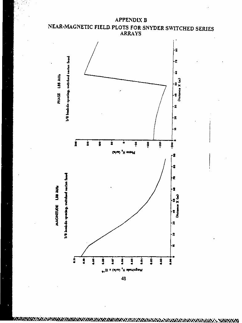
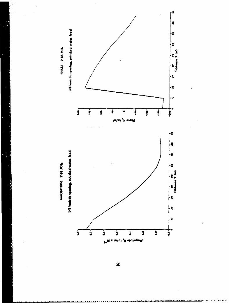
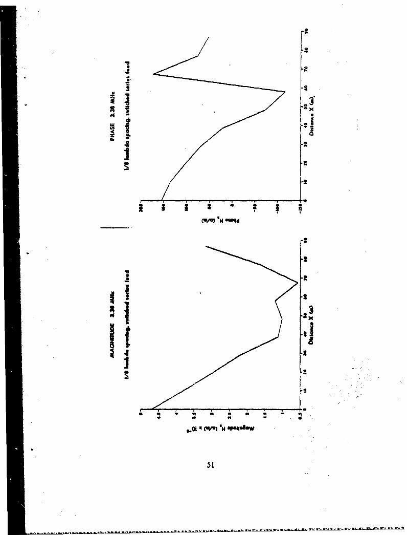
APPENDLX BNEARR-tMAGNETIC FIELD, PLOTS FOR SNYDER SWITCHED SERIES
ARRAYS
I_0 (W/), / "a
- 4
I||
48

I.
1.I., ! "i0
•i i~i ii ,,.,ii i 'I '' I'+
• . I l "H ui~o +a
~ 1 1 29
*r *
* p
4 /
Ii.4
/ i•2
500
*15S• w 2
a
0
* 0* N
0'
a0
03*
ax0g
OW.9-
aC
4 0
Ift
I I , �
*
t
II3
If *1I
'9. � 0
C�,,) '14 P4P�W
5!
+.P
i ! i
IIIS* 2
+Za
t *t1
-- - " •lllllli0
V" "
. _ ,. • I . - • 9
U, at
1 , 0 f
$33
I. a*10 4
- - -
- 0m
0 0z 1a./) H•IU~
54a
S• ~~, _•

4 -
* O
I III
4 .32
•I e A iI -• ;
C.01*.0 (0/0) 'N4 M6muW
55

-=ii•=_0
_• •
3
(U/fl) 'H 'RX~d
I
to
56
,0
* .e
0..
.£
111
F..
0
,t
0O -N0o
• • •
4-8
I.
I ii ,,,
0ft
1'* N
a ,4I / '3
t.lI• 'H v•
o0
- C
i! J-
610
0 -n
I 0
62a

j .:*
0.. 0
z *
a 0i
£1~3
•,•,•v• '•.•'• • k• • • • '• •• • • ••-••( _ _ _. .. . .__ •
£ /!
, o
*.
U••
,I
0 H*0 i
i -a I
a-:
_ •-- ---- •.
i .,Oi •c"• I+4+0
* a
!£

0 F•
p. -
a.if
1 3
* a •
II
I..-t

ii a
It a
' ' " "
: 1.:
g4
. 3 -"
67
|a
|C
MI ., .
i ?,,,/* zH $osod
in
w CC4
68
AXII.AAAWMA( ,klAW Vk U k*.VVIA%,t'kv A. lLk

0o
--- -- '0
• ml m
• [ .
m
J0
\0
- 69
"5~
it me) "Us
00
07
q ~nnWq • Jxi l ii lmal~l l~L• ~ ll~qmlilllmlO ll l lL ::: : ":llI l~ll • l lw~~mwllm_• . i '
060
lao,
£ 1 71

- •a
iC
I-a
, ; : * I(W/S) H •' 4d '
72g
w
.1
SI I Ia.;
4
*1 [I0 0
-J..
4aus
da;a 1.
', •.01 (/rn t 4 l .l
J0
74
Im| i n )m m mum i mamp m ~ mm ~ m mne~a mmmu~arupup m nm m ~ ml n amq
* C'
0?
Ix
*7 -L
I VI
=.r•( r H°uu°
* T6i,0VI
i Mmm - umnnmm ummJ,,mnllm ~ m,, v..l•.,m~m,. .0

• C.
* 'EqlI a•l
3'7
* 0
CN
EqF aEq* 1��
* Eq* I:* Eq
C
*7 GA
t
I aN
C0
a4..
'0
II: *
14 '814d
Ii F!Eq
II
�x3a'I AIaN
1.� Eq 04 04 04 - 04 0
.9
9.01 ' 14 SP�IW�SW
78
a
'[CA
-
x
-
0 L " 2 • - • . • • ,
Ik
11 1
* t i t .L . . . 1 iI I : I •
8.0 U uV' '4 op ftw goW
"79
•~I7
*1 -'I
i t•
Ii" s. /
Ii 7•.
- *
I ..I . ." I
a * ' 4, 0i~l .4U 4 0 9,
80

* eq
IiI
: ;~ ~ _ _ _ Z T -- • I • -L _ : -.. .J ;• ' T _: I L .T 3 ._ . : ; _ • " " _ -_ '.L . .. • . .: '' . .-- : .. .. .• .. -I_ .= _ _ _ -_ L • ._

I r
= aj. U
• . ,.• . ,.,,
C 2 , 0 C(4I -
(•/D) 'H otDn~d
C
o a*O I(')"H•nluo
N 2.IPII
"- . . ... . . . . . .. . . . . ... + . . . .
a•
-- o
o a
- .
o33
a
° • :•o • °
* Cl
0t J l
- |a(;I')x emlS•
0 84
**
(,.,
- i • i' i u ' ; 0
, 0.3"2
I InI,- i i "
* O0 • H°P~u~
NS
S.. ... • m flIf IN mIb • M I mm•h~li~ Dm •Um il i p l • i -:.• " U._!•-._ i e ili0

00C4
CA C
I -n
""
N0 x Cw/ c) "N opn;luS*W
86+
APPENDLX CNEAR-MIAGNETIC FIELD PLOTS FOR SNYDER SWITCHED
PARALLEL ARRAYS
.. 9
CWM/ =H ""qd "
w0
ch~
0t
o. "
0
U,' ,-
"•.01 x cw/0) 'N sJPnausaw
87
* 0•
< N.
0 4
* =
N U
I if | i , l i .'
"I 0
.20
4.4
* .0
C.,
49
I
.01cw/o) "N* opn 44dg
98
/---
n 3 i ll n u
9.O1 x 'N o)t p"~UsoW
90
I.
$ .u
IM4'
.1 91
o 0 0 0 0
- 0
CU/U (lt) tH '4 4dO
99
I
-- S
- "4w -.
• [.2
4 ft i : i
49
9.0
9 &i
933
ia
*t~
49
mNW~m••m m •

/
IlI-
<0 /
N '4d
*
95
-•,•,",-•o•. L-. 3 °
.- a
0 3Z10
J "-
-,-
0'
a
* 0N
400.
@30w 0
* UC
00ii. a4'
-ft0
; ; : *- t
':'/g)
0
2KaII 2
3IIAIi 2I
* 1 1 � � � I
K (U/o� SPI4WOSW
97
N 0.
.50
* 03
! i
U 0"
a 0
*1.0 I,' .nluo
A 08
|0

966
13
x
01 /o x O N epusod
* •
Ma
0'0
•.IxO/• H••lo
99S
i i
VC
.it Vo) 'm ""Uso-
'10

vq
ft
ii
1 I .I
US! 5 .5
10II

ii
0 ~ -- U
*1 S2
ii 'q. E I l l _]' ] :l i I l l m I ~ l l l I l l l l
"*0 I
, , I"
("0 i
M
IL
CL
114ii!
F
9t
Sebe
./.
'C [ i i i i ....
0. ('I'C/) '14 qgp
.10
.41ev it rM *Nwso
10
0
"so.
1 :3
~, I u
i!
-s '14 "iNed
107
Sn 0
CLC
ILI
/*"C
.. 3
U x
I4i6 ,"i .
108
IL __ _ + - . ... . . ... .. . . . .. ... . ...i, imm~qll lw rmlrtm .• ••:•+: N+
.0
0
(.., (Vo ', PxB°
10.0
N •.~q . .
,0.
a.1
. "if
mx
SI"I
I]

00
-;I
/ 0.
0 a,, ,, . . .. . . ' Z
4 ° ° x, ° • }
0 --
-4,E
Uiw ":a
41

N fl.
w
3110

Is -'
9L-i 0
S...... O/0) N" " w'
114
S• Lg
0.!
.11*
IL. . . .. ..i II • I I W I• I I I l lll l I I cs/uil p
cl
-2
.!u
ti
"w a
to.l meu ) 'X"Wl' ow
116
i m m i
lrr imui m • m ::w
C
... ; -m -ie• w~ m . ,m . ul•.
460
vs0
CW" w *M
0L
11

-4
,40t
I K.
14'1
--- 1
'II
1 II li t ,m 4 ,v • o
115

3 ; ; ..
S119

K9* KI1
11 Kj
Ii KN4.,
I.U I 0 0 00 0 0 0
:1It Ig
33;"(a U'AII
�0
i- i �0
,.Ot�cw'� I4"PE4�6W
120
494
itH
I *
Ix
*W SVI,*4'l0 ,
12i1
*12
-]I.
- .- . +. , .
w o-
,Cn 'r
• 0
:. .J.,+.. !
a I
-I /
122
-- _ - , . .. .. ;. -,, . . ..... . .. .
90
SC'S
Si 0.• -r ~ I0
S10'1-; -
0
9..mt 0) "N apnifusow
123
0 F!C.
a
cwmH Wmd
0 0.01 .0) IH 6otluBaw
124
.= .~.• qu
*0
00
00
0I
01 1�0 �"4
0�
I"4
(u/') 'N W4id
a
a�2
ii I
I�
II
0-5*.OI ('/) 'H 9141U@W
125
I I°AL-==w •
I.
wa
!13
iII
Ii
iI :
126
4.
w -"4$ 4 0 -rI D g " ,D • o -
o,.OIt • 0
* 0 0 0 0 010
o~ ani m al Igi 4m rww
ci"3IL
a 20
I2ZI
12

u0B
00
it4
-D h I• "
129
1 .

a
.j .,
w "
S..
*30
; n
4.Sa.!
S, ,S, ,
w3
APPENDIX DNEAR-MAGNETIC FIELD PLOTS FOR SNYDER UNSWITCHED
PARALLEL ARRAY
Va
"m oww
!13
132

Ii
g i *- 0 i L I
I F
.I
I .
.4 5 - 5 1 -
133
"0*
.2
I I
Cu/,""w H ""d
,ý.Ojx Me) 'M ftft12
134
*4
-l -
'--. F;I K • !
/3
lu a
'0 "
. ....
I --
_ _ _ _ _x (We/) NH opntlusw
136
- a
_-__-
-- 0.,
< ';
=0 . , , , , , . , ,, ,
.8!
I,
IaII I i I i ii i I I I i l. .
413
IL'
0
44
0F
-f 19 -u ow w . ,•
a138
a. ,• •!o
"L"
0
-I
C..) *•o t p•h
:11

!:..
:] ~i
Q,,~
i me--- "r. -•
I
_____€___ (3/0 'H luOW~
-_- •0
CM0 H:""""
Ix
S14111 3
C
0I
00
CI. Ua0.
N
-� 3 xw - 0
'I
CaC-
0
C
a *
(W/0) 14 01O44�
Cb
I09
a
* *Ji 4S
1..O (�/) '�4 P�4P�'W
142
- 3.Stt�.tPMtU%'tA.1fli �..f'.. .P : � � 's,,ss, .rC
iC.,
a.
! "i
- 0U
.. !
I '
I I
04
i i''
U 0:
1*4
~I I . ....
n0
-'•6 N ""d
4 06
01 mm 'N opwao
145

* I
! I 'ALi
*.. d i" ,, .6w
14 '

APPENDIX E
NEAR-MAGNETIC FIELD PLOTS FOR STANDARD ELEMENT ARRAYS
IIn
- i2x
.-01* s.0 mm 'N4 ,mqvow1
147
(I I
hb
46 4i 4MI ow-oue
1484
-F!
39
;423
,0(
149
C,
aC4
(4
C4
0 '0 0 00 0
U" , ..
a
'W/o) iq op~mlsad
n150

,a1
1 C4
-89ax
.3C4
o Ix
90 (W/O
0*0
M= .5 '.4� '.4
.q. _o - 0
*q* -�
0In a.
= .��
0Uo
I- W'- C
< .�
.3;.U
o .5N
C 0
U,
� ; :. *
11�q.
Ii I3
if NiA0
I N
2 9 Vt I *t 0U N
9.01 3(UyS) ')4 P'44'8 'W
152
p p p

i 0
ft
CLC
153
23
II

i - [ --
x "~
g 2 0
I i , ,,. M (z,• " .pn!•3
4'N
0
0
a F;33
=0UC
0-4'-
a. -a
I 'I
o* *
I 9
C�/') 14 '4d
I.;0
'S.0
ii a
IIf 'A
I
/ '04'
I I I.3 3 2 k I � I0.:: �
� (W) H
155
ii
= "~
| .f
I • ll l , ..2 • I
(..4 X I I•
150

0
C,
0C,0
00
:23n 0
Ii a
I I(.4
04
0 0 0 0 0 0 0� 21 & � ? q
________________ ('V.) 'H 0W8I4�
£
I I*
It a
ft II I
1�0
� 0
157

S°•I '
.=
a
151

0
[1
-- 2
a
*15,f i
____i
" II
(.
•'1 59
a

0
00
If.,0 I
'4 0. I
I�3=
'q� 3�
II r01
* [0* a*49
__________ ('S/W) 'N .8MW
I.
I1*
ii £
'2
ifI / -;'I..
I a '0 *9 S
' 14 P�a#&w
160

- C0
• u
_--a'....
I_._ ,...
LIST OF REFERENCES
S1. Johnson, Richard C. and Jasik, Henry, Antenna Engineering Handbook, McGraw-Hill Book Company, New York, 1984.
S2. Stutzman, Warren L., and Thiel•, Gary A., Antenna Theory and Design, JohnWiley and Sons, New York, 1981.
3. Rumsey, Victor H., Frequency Independent Antennas, Academic Press, New York,1966.
4. Johnsen, John Richard, An Investigation into the Potential for Developing aSucces.Xf'd Log-periodic Half Square Antenna with Dual-feed, MSEE Thesis. NavalPostgraduate School, Monterey, California, December 1986.
5. Snyder, Richard D., Broadband Antennae Employing Coaxial Transmission LineSections, U.S. Patent 4.479,130, 23 October 1984.
6. Naval Ocean Systems Center Technical. Document 116 volume 2, ,NumericalElectwomagnetics Code (NEC).Method of Moments, January 1981.
7. Hansenr, Robert C., 'Evaluation of' the Snyder Dipole', IEES 7Tansactions anAntennas and Propagation, voL AP-35, no. 2, February 1987.
8. Coln, Robert E., and Zucker, Fran.i2 J., Antenna ThAeuy Part 2, McGraw-HiglBook Company, New York, 1969.
9. ,Miurra, Raj and Jones, Kenneth E., 'How to Use k-fl Diagrans in Log-PeriodicAntenna Designi, Microwaves, pp; 18-26, June 1965.
162
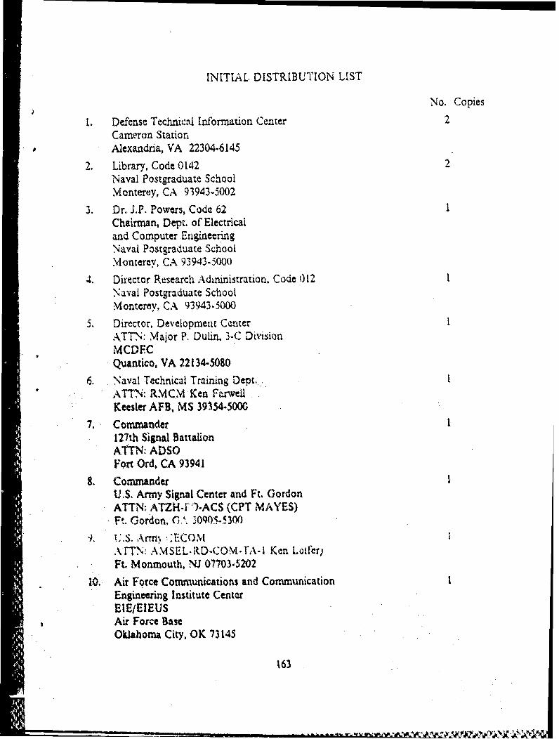
INITIAL. DISTRIBUTION LIST
No. Copies
1. Defense Technical Information Center 2Cameron StationAlexandria, VA 22304-6145
2. Library, Code 0142 2Naval Postgraduate SchoolMonterey, CA 93943-5002
3. Dr. J.P. Powers, Code 62Chairman, Dept. of Electricaland Computer EngineeringNaval Postgraduate SchoolMonterey, CA 93943-5000
4. Director Research Administration. Code 012Naval Postgraduate SchoolMonterey, CA 93943-5000
5, Director, Developmeat CenterATTN: Major P. Dulin. 3-C DivisionMCDECQuantico, VA 22134-5080
6. Naval Technical Training Dept.,ATTN: RMCM Ken Farwel .Keesler AFB, MS 39354-5000
7.-Commander127th Signal BattalionATTN: ADSOFort Ord, CA 93941
8. CommanderU.S. Army Signal Center and Ft. GordonATTN. ATZHf{'-),ACS (CPT MAYES)Ft. Gordon, 0.% 30905-5300
• . ;.S. ArmN -.'ECOM%,
\"TTN: AMSL.-RD-COM-- r..- I Ken Loiter)Ft, Monmouth, NJ 07703-5202
10. Air Force Communications and CommunicationEngineering Institute CenterEIE/EIEUSAir Force BaseOklahoma City, OK 73145
163
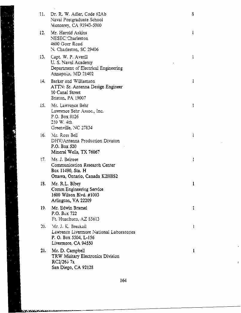
11. Dr. R. W. Adler, Code 62AbNaval Postgraduate SchoolMonterey, CA 93943-5000
12. Mr. Harold AskinsNESECiCharleston4600 Goer RoadN. Charleston, SC 29406
13. Capt. W. P. AverillU. S. Naval AcademyDepartment of Electrical EngineeringAnnapois, MD 21402
14. Barker and WilliamsonATTN: Sr. Antenna Design Engineer10 Canal StreetBriston, PA 19007
15. Mr. Lawrence BehrLawrence Behr Assoc., Inc.P.O. Box 80262 1,0 W. 4thGreenville, NC 27834
16. Mr. Ross BellDHV/Antenna Production DivisionP.O. Box 520Mineral Wells, TX 76067
17. Mr. J. BeiroseCommunication Research CenterBox 11490, Sta. HOttawa, Ontario, Canada K2H8S2
18. Mr. R.L. BibeyComm Engineering Service1600 Wilson Blvd. #1003Arlington, VA 22209
19. Mr. Edwin BramelP.O. Bux 722Ft. Huachuca, AZ 85613
20. Mr. J. K. BreakallLawrence Livermore National LaboratoriesP. 0. Box 5504, L-156Livermore, CA 94550
21. Mr. D. CampbellTRW Miditary Electronics DivisionRC2/266 7xSan Diego, CA 92128
164

22. Mr. Al Christman / Rodger Radcliff 2Ohio UniversityClippenger Research LaboratoryAthens, OH 45701
23. Mr. R. CorryUSACEEIACCC-CE-TPFt. Huachuca, AZ 85613
24. Mr. Lee W. CorringtonCommander USAISEICATTN: ASBI-STSFt. Huachuca, AZ85613-7300
25. Dr. Roger A. CoxTELEX Communications, Inc.8601 Northeast Hwy 6Lincoln, NE 68505
26. Mr. Pete CunninghamDRSEL-COM-RN-4CENCOM-CENCOMSFt. Monmouth, NJ 07703-5202
27. Mr. W. DecormierDielectric ProductsTower Hill RoadRaymond, ME 04071
28. Mr. E. DomingLawrence Livermore National LaboratoryP. 0. Box 5504, L-153Livermore, CA 94550
29. Mr. R.P. EckertFED COMM COMM2025 M Street, NWWashington, D.C. 20554
30. Mr. D. FaustEyring Research Institute1455 W, 820 N.Provo, UT 84601
31. Dr. AJ. FerraroPenn State Univ.Ionosphere Res. LabUniversity Park, PA 16802
32. D. FessendenNaval Underwater Systems Ctr
165
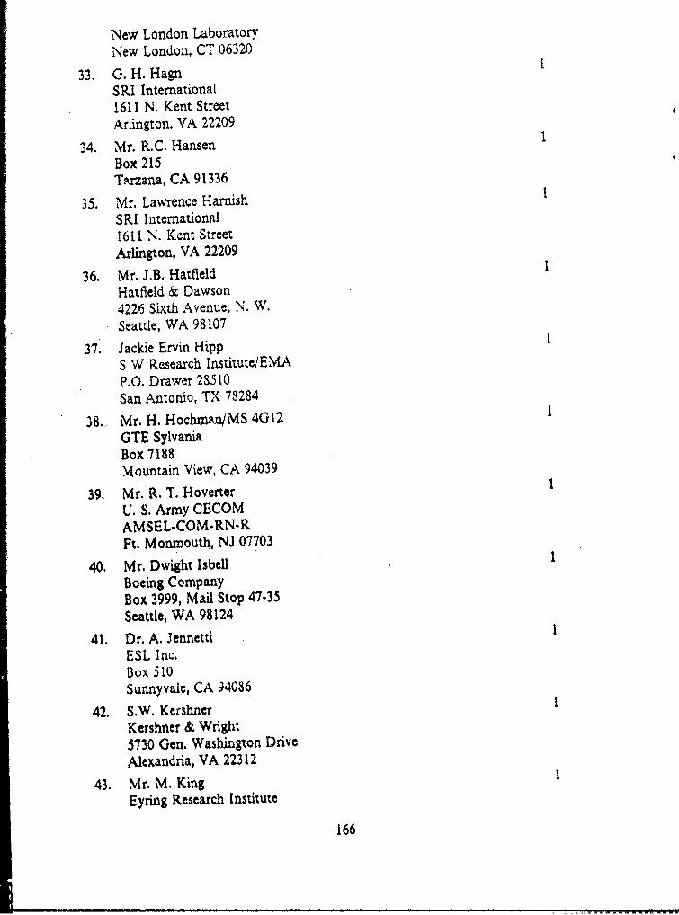
New London LaboratoryNew London, CT 06320
33. G. H. HagnSRI International1611 N. Kent StreetArlington, VA 22209
34. Mr. R.C. HansenBox 215Tarzana, CA 91336
35. Mr. Lawrence HarnishSRI International1611 N. Kent StreetArlington, VA 22209
36. Mr. J.B. HatfieldHatfield & Dawson4226 Sixth Avenue, N. W.Seattle, WA 98107
37. Jackie Ervin HippS W Research Institute/EMAP.O. Drawer 28510San Antonio, TX 78284
38. Mr. H. Hochman/MS 4G12GTE SylvaniaBox 7188Mountain View, CA 94039
39. Mr. R. T. HoverterU. S. Army CECOMAMSEL-COM-RN-RFt. Monmouth, NJ 07703
40. Mr. Dwight IsbellBoeing CompanyBox 3999, Mail Stop 47-35Seattle, WA 98124
41. Dr. A. JennettiESL Inc.Box 5 10Sunnyvale, CA 94086
42. S.W. KershnerKershner & Wright5730 Gen. Washington DriveAlexandria, VA 22312
43. Mr. M. KingEyring Research Institute
166

1455 W. 820 N.?rovo, UT 84601
44. H. Kobayashi1607 Cliff DriveEdgewater, MD 21037
45. Dr. H. M. Lze, Code 62LhNaval Postgradua, SchoolMonterey, CA 93943-5000
-16. Mr. George LaneVoise of America/ESBA601 D. Street, NWWashington, DC 20547
47. Mr. Jim LilyLitton/Amecon5115 Calvert RoadCollege Park, MD 20740
-48. Mr. J. Logan, Code 822 (T)Naval Ocean System Center271 Catalina BoulevardSar, Diego, CA 92152
49. R. LuebbersPenn State UniversityEE DepartmentUniversity Park, PA 16802
50. Ms. Janet McDonaldUSAISESAASBH-SET-PFt. Huachuca, AZ 85613-5300
51. Mr. B. John Meloy333 Ravenswood /Pldg. GMenlo Park, CA 94025
52. E.K. MillerRockwell Science CenterBox 1085Thousand Oaks. CA 91365
53. Mr. L.C. MinorlIT Research lnst./,ECAC185 Admiral Cochrane Dr.Annapolis, MD 21401
54. J. MolnarSpace and Naval Warfare Systems CommandCode G141National Center #1
167

Washington, DC 20363
55. Mr. Wes Olsen2005 Yacht DefenderNewport Beach, CA 92660
56. Mr. D. J. Pinion74 Harper StreetSan Francisco, CA 9413i
57. C.E. PooleFCC/Field Pens Bur555 Battery Street Rm. 323ASan Francisco, CA 94111
58. Mr. J. J. Rea ves Jr.Naval Elec. System Engineering Center4600 Marriott DriveN. Charleston, SC 29413
59. Mr. A. ResnickCapital Cities Communication, ABC Radio1345 Avenue of Americas / 26th FloorNew York, NY 10705
60. R.3. Riegel8806 Crandall RoadLanham, MD 20801
61. Dr. J. W. Rockway, Code 8112 (T)Naval Ocean System Center27t Catalina BoulevardSan Diego, CA 92152
62. Mr. Joseph R. RomanoskyNational Security Agency/R632Electronic EngineerFt. Meade, MD 20155
63. R. RoyceNaval Research LaboratoryWashington, DC 20375
64. Dr. Jacob Z. SchankerScientific Radio Systems367 Orchard StreetRochester, NY 14606
65. Mr. T.B. Sullivan108 Market StreetNewburgh, IN 47630
66. T. SimpsonUniv, of S. CarolinaCollege of Engineering
168
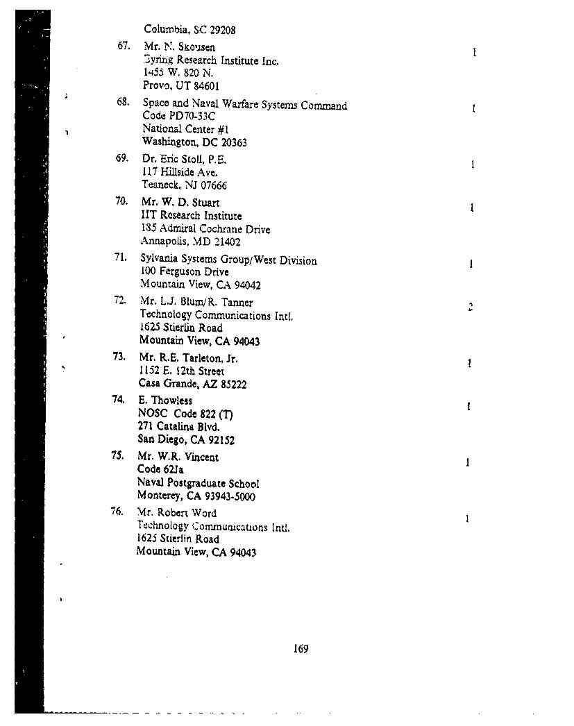
Columbia, SC 2920867. Mr. N. Siousen
Zyring Research Institute Inc.1-455 W. 820 N.Provo, UT 84601
68. Space and Naval Warfare Systems CommandCode PD70-33CNational Center #1Washington, DC 20363
69. Dr. Eric Stoll, P.E.117 Hillside Ave.Teaneck, NJ 07666
70. Mr. W. D. StuartIIT Research Institute185 Admiral Cochrane DriveAnnapolis, MD 21402
71. Sylvania Systems Group/West Division100 Ferguson DriveMountain View, CA. 94042
72. Mr. LJ. Blum,/R. TannerTechnology Communications Intl.1625 Stierlin RoadMountain View, CA 94043
73. Mr. R.E. Tarleton, Jr.1152 E. 12th StreetCasa Grande, AZ 85222
74. E. ThowlessNOSC Code 822 (T)271 Catalina Blvd.San Diego, CA 92152
75. Mr. W.R. VincentCode 621aNaval Postgraduate SchoolMonterey, CA 93943.5000
"76. Mr. Robert WordTechnology Commuaications Incl.1625 Stierfin RoadMountain View, CA 94043
169