Embed Size (px)
Citation preview

NAVAL
POSTGRADUATE SCHOOL
MONTEREY, CALIFORNIA
THESIS
Approved for public release; distribution is unlimited
AN IMPROVED RECTENNA FOR WIRELESS POWER TRANSMISSION FOR UNMANNED AIR VEHICLES
by
Chun-Yi Liu
September 2011 Thesis Advisor: David C. Jenn Second Reader: Ric Romero

THIS PAGE INTENTIONALLY LEFT BLANK

i
REPORT DOCUMENTATION PAGE Form Approved OMB No. 0704-0188Public reporting burden for this collection of information is estimated to average 1 hour per response, including the time for reviewing instruction, searching existing data sources, gathering and maintaining the data needed, and completing and reviewing the collection of information. Send comments regarding this burden estimate or any other aspect of this collection of information, including suggestions for reducing this burden, to Washington headquarters Services, Directorate for Information Operations and Reports, 1215 Jefferson Davis Highway, Suite 1204, Arlington, VA 22202-4302, and to the Office of Management and Budget, Paperwork Reduction Project (0704-0188) Washington DC 20503.
1. AGENCY USE ONLY (Leave blank)
2. REPORT DATE September 2011
3. REPORT TYPE AND DATES COVERED Master’s Thesis
4. TITLE AND SUBTITLE An Improved Rectenna for Wireless Power Transmission for Unmanned Air Vehicles
5. FUNDING NUMBERS
6. AUTHOR(S) Chun-Yi Liu
7. PERFORMING ORGANIZATION NAME(S) AND ADDRESS(ES) Naval Postgraduate School Monterey, CA 93943-5000
8. PERFORMING ORGANIZATION REPORT NUMBER
9. SPONSORING /MONITORING AGENCY NAME(S) AND ADDRESS(ES) N/A
10. SPONSORING/MONITORING AGENCY REPORT NUMBER
11. SUPPLEMENTARY NOTES The views expressed in this thesis are those of the author and do not reflect the official policy or position of the Department of Defense or the U.S. Government. IRB Protocol number NA.
12a. DISTRIBUTION / AVAILABILITY STATEMENT Approved for public release; distribution is unlimited
12b. DISTRIBUTION CODE A
13. ABSTRACT (maximum 200 words)
This thesis continues an NPS project related to wireless power transmission for micro air vehicles (MAVs). The conversion of radio-frequency (rf) power into usable direct-current (dc) power is performed by a rectifying antenna, or rectenna. The emphasis of this thesis is the simulation and experimental study of various rectenna designs to determine which best provides high efficiency, stable output power, and lightweight design.
The analysis of rectenna design focuses on four subsystems: (1) the receiving antenna, (2) the matching sections, (3) the rectification, and (4) the post-rectification filter. Based on the findings of this research, the ultimate rectenna design implements a half-wave dipole antenna that performs full-wave rectification with two diodes. The post-rectification filter is implemented by a capacitor to obtain stable dc power. The final design achieved an efficiency of nearly 66% for input power in the range of 200 mW.
14. SUBJECT TERMS Rectenna, Wireless Power Transmission, Dipole Antenna, MAV 15. NUMBER OF
PAGES 95
16. PRICE CODE
17. SECURITY CLASSIFICATION OF REPORT
Unclassified
18. SECURITY CLASSIFICATION OF THIS PAGE
Unclassified
19. SECURITY CLASSIFICATION OF ABSTRACT
Unclassified
20. LIMITATION OF ABSTRACT
UU
NSN 7540-01-280-5500 Standard Form 298 (Rev. 2-89) Prescribed by ANSI Std. 239-18

ii
THIS PAGE INTENTIONALLY LEFT BLANK
iii
Approved for public release; distribution is unlimited
AN IMPROVED RECTENNA FOR WIRELESS POWER TRANSMISSION FOR UNMANNED AIR VEHICLES
Chun-Yi Liu Captain, Republic of China Army
B.S., Chung Cheng Institute of Technology, 2005
Submitted in partial fulfillment of the requirements for the degree of
MASTER OF SCIENCE IN ELECTRONIC WARFARE SYSTEMS ENGINEERING
From the
NAVAL POSTGRADUATE SCHOOL September 2011
Author: Chun-Yi Liu
Approved by: David C. Jenn Thesis Advisor
Ric Romero Second Reader
Dan C. Boger Chair, Department of Information Science

iv
THIS PAGE INTENTIONALLY LEFT BLANK

v
ABSTRACT
This thesis continues an NPS project related to wireless power transmission for micro air
vehicles (MAVs). The conversion of radio-frequency (rf) power into usable direct-current
(dc) power is performed by a rectifying antenna, or rectenna. The emphasis of this thesis
is the simulation and experimental study of various rectenna designs to determine which
best provides high efficiency, stable output power, and lightweight design.
The analysis of rectenna design focuses on four subsystems: (1) the receiving
antenna, (2) the matching sections, (3) the rectification, and (4) the post-rectification
filter. Based on the findings of this research, the ultimate rectenna design implements a
half-wave dipole antenna that performs full-wave rectification with two diodes. The post-
rectification filter is implemented by a capacitor to obtain stable dc power. The final
design achieved an efficiency of nearly 66% for input power in the range of 200 mW.

vi
THIS PAGE INTENTIONALLY LEFT BLANK

vii
TABLE OF CONTENTS
I. INTRODUCTION........................................................................................................1 A. BACKGROUND ..............................................................................................1 B. OBJECTIVE ....................................................................................................2 C. THESIS OUTLINE ..........................................................................................3
II. BACKGROUND ..........................................................................................................5 A. EARLY EXPERIMENTS WITH WPT .........................................................5 B. RECENT DEVELOPMENTS IN WPT .........................................................8 C. RECENT RESEARCH IN RECTENNAS.....................................................9 D. PREVIOUS NPS RESEARCH .....................................................................12 E. SUMMARY ....................................................................................................13
III. RECTENNA DESIGN ...............................................................................................15 A. DISCUSSION OF RECTENNA DESIGN ...................................................15
1. General Rectenna Design ..................................................................15 2. Antenna Design ..................................................................................19 3. Power Budget .....................................................................................23
B. COMPARISON OF DIFFERENT DESIGNS USING ADS ......................25 1. Half-Wave-Rectification Rectenna Design ......................................26 2. Hybrid Rectenna Design ....................................................................32 3. Full-Wave Rectenna Design ..............................................................38 4. Conclusion ..........................................................................................44
C. EVALUATION OF HARMONIC FREQUENCIES ..................................44 1. Harmonic Balance Analysis for the Half-Wave Rectenna .............45 2. Harmonic Balance Analysis for the Full-Wave Rectenna ..............51 3. Findings ...............................................................................................59
IV. RECTENNA IMPLEMENTATION ........................................................................61 A. RECTENNA IMPEDANCE DESIGN .........................................................61
1. Full-Wave Rectenna Design ..............................................................61 2. Performance of Full-Wave Rectenna Impedance Design ...............62
B. CIRCUIT LAYOUT AND TUNING ...........................................................64 1. Circuit Design Layout........................................................................64 2. Calculation of the Matching Unit .....................................................65
V. SUMMARY, CONCLUSIONS AND RECOMMENDATIONS ...........................71 A. SUMMARY ....................................................................................................71 B. RECOMMENDATIONS ...............................................................................71
1. Using High-Power Transmitter and High-Gain Antenna ..............71 2. Building a Hardware Prototype .......................................................72 3. Running Simulations for an Array ...................................................72 4. Reducing Polarization Loss ...............................................................72
LIST OF REFERENCES ......................................................................................................73
INITIAL DISTRIBUTION LIST .........................................................................................75

viii
THIS PAGE INTENTIONALLY LEFT BLANK
ix
LIST OF FIGURES
Figure 1. Conceptual powering of an MAV by a ground station (From [6]). ...................2 Figure 2. Generic WPT-system block diagram. ................................................................5 Figure 3. Experiment with radio waves for power transmission (From [1]). ....................6 Figure 4. A helicopter powered by WPT (From [1]). .......................................................7 Figure 5. Satellite solar-power model (From [14]). ..........................................................8 Figure 6. Circuit configuration of the dual-frequency rectenna (From [15]). ...................9 Figure 7. Block diagram of the conventional and the proposed rectenna (From [17]). ..10 Figure 8. Full-wave rectification (From [19]). ................................................................11 Figure 9. Circuit design of the rectenna (From [20]). .....................................................12 Figure 10. Basic configuration of NPS rectenna system (From [7]). ................................15 Figure 11. 11S frequency response of circular-patch antenna design (From [7]). .............16
Figure 12. Simulated response of sixth-order low pass filter using ADS software (From [7]).........................................................................................................17
Figure 13. Simulated response of Schottky diode using ADS software (From [7]). .......18 Figure 14. Two views of the half-wave, dipole-antenna structure. ...................................20 Figure 15. 11S frequency response of half-wave, dipole-antenna design. .........................21
Figure 16. Smith chart of the half-wave, dipole-antenna design. ......................................22 Figure 17. Three-dimensional, far-field radiation pattern of the half-wave, dipole-
antenna design. .................................................................................................23 Figure 18. Diagram of the transmit antenna and rectenna. ...............................................23 Figure 19. Required transmitting power versus distance with 200 mW received power.
..........................................................................................................................25 Figure 20. Block diagram of half-wave rectification rectenna (From [22]). .....................26 Figure 21. ADS S-parameter circuit model of Toh’s rectenna (From [7]). .......................26 Figure 22. ADS model of a half-wave rectenna design with a pre-LPF. ..........................27 Figure 23. ADS model of a half-wave rectenna design with a post-LPF. .........................28 Figure 24. ADS model of a half-wave rectenna design without LPF. ..............................28 Figure 25. Output power (watts) versus time for a half-wave rectenna design with a
pre-LPF. ...........................................................................................................30 Figure 26. Output power (watts) versus time for a half-wave rectenna design with a
post-LPF. ..........................................................................................................30 Figure 27. Output power (watts) versus time for a half-wave rectenna design without
LPF. ..................................................................................................................31 Figure 28. Conversion efficiency of simulated half-wave rectenna designs using ADS.
..........................................................................................................................32 Figure 29. Block diagram of hybrid rectenna (From [18]). ...............................................33 Figure 30. ADS model of a hybrid rectenna design with a pre-LPF. ................................34 Figure 31. ADS model of a hybrid rectenna design with a post-LPF. ..............................35 Figure 32. ADS model of a hybrid rectenna design without LPF. ....................................35 Figure 33. Output power (watts) versus time for a hybrid rectenna design with a pre-
LPF. ..................................................................................................................36
x
Figure 34. Output power (watts) versus time for a hybrid rectenna design with a post-LPF. ..................................................................................................................36
Figure 35. Output power (watts) versus time for a hybrid rectenna design without LPF. ..................................................................................................................37
Figure 36. Simulated conversion efficiency of the hybrid rectennas. ...............................38 Figure 37. Block diagram of full-wave rectifier (From [23]). ...........................................39 Figure 38. ADS model of a full-wave rectenna design with a pre-LPF. ...........................40 Figure 39. ADS model of a full-wave rectenna design with a post-LPF. .........................40 Figure 40. ADS model of a full-wave rectenna design without LPF. ...............................41 Figure 41. Output power (watts) versus time for a full-wave rectenna design with a
pre-LPF. ...........................................................................................................42 Figure 42. Output power (watts) versus time for a full-wave rectenna design with a
post-LPF. ..........................................................................................................42 Figure 43. Output power (watts) versus time for a full-wave rectenna design without
LPF. ..................................................................................................................43 Figure 44. Simulated conversion efficiency of full-wave rectenna using ADS with
different LPF. ...................................................................................................44 Figure 45. Harmonic balance of configuration in half-wave rectenna with pre-LPF. ......45 Figure 46. Simulated input power, reradiated harmonic powers, and dc power (in
dBm) versus frequency for the half-wave rectenna with pre-LPF. ..................46 Figure 47. Harmonic balance simulation configuration for the half-wave rectenna
with post-LPF...................................................................................................47 Figure 48. Simulated input power, reradiated harmonic powers, and dc power (in
dBm) versus frequency for the half-wave rectenna with post-LPF. ................48 Figure 49. Harmonic balance simulation configuration for the half-wave rectenna
without LPF. ....................................................................................................49 Figure 50. Simulated input power, reradiated harmonic power, and dc power (in
dBm) versus frequency for the half-wave rectenna without LPF. ...................50 Figure 51. Harmonic-balance simulation configuration for the full-wave rectenna
with pre-LPF. ...................................................................................................51 Figure 52. Simulated input power, reradiated harmonic power, and dc power (in
dBm) versus frequency in full-wave rectenna with pre-LPF. ..........................52 Figure 53. Harmonic-balance simulation configuration for the full-wave rectenna
with post-LPF...................................................................................................54 Figure 54. Simulated input power, reradiated harmonic power, and dc power (in
dBm) versus frequency for the full-wave rectenna with post-LPF. .................55 Figure 55. Harmonic-balance simulation configuration for the full-wave rectenna
without LPF. ....................................................................................................57 Figure 56. Simulated input power, reradiated harmonic power, and dc power (in
dBm) versus frequency for the full-wave rectenna without LPF. ....................58 Figure 57. Final circuit design of full-wave rectification rectenna. ..................................61 Figure 58. Simulated output power, voltage, and current-versus-time for the full-
wave rectenna with a 23 dBm input. ................................................................62 Figure 59. Conversion efficiency of final full-wave rectenna design. ..............................63 Figure 60. Output power (watts) of final full-wave rectenna design. ...............................63

xi
Figure 61. Final circuit layout of the full-wave rectenna modeled in CST. ......................64 Figure 62. Circuit diagram showing the stub position. .....................................................66 Figure 63. CST model of the circuit. .................................................................................68 Figure 64. 11S frequency response of full-wave rectenna using CST. ..............................68
Figure 65. Simulated result of the far-field radiation of full-wave rectenna using CST. ..69

xii
THIS PAGE INTENTIONALLY LEFT BLANK

xiii
LIST OF TABLES
Table 1. Measured data for the MAV motor (From [7]). ...............................................19 Table 2. Design specifications for the half-wave dipole antenna. .................................21 Table 3. Harmonic balance data for the half-wave rectenna with pre-LPF. ..................47 Table 4. Harmonic balance data for the half-wave rectenna with post-LPF. .................49 Table 5. Harmonic-balance data for the half-wave rectenna without LPF. ...................51 Table 6. Harmonic balance data for the full-wave rectenna with pre-LPF. ...................53 Table 7. Harmonic-balance data for the full-wave rectenna with post-LPF. .................56 Table 8. Harmonic-balance data for the full-wave rectenna without LPF. ....................59 Table 9. Properties of Rogers Duroid 5880LZ. .............................................................65

xiv
THIS PAGE INTENTIONALLY LEFT BLANK

xv
LIST OF ACRONYMS AND ABBREVIATIONS
ADS Advanced Design System
BPF Bandpass Filter
CST Computer Simulation Technology
CW Continuous Wave
dc Direct Current
DARPA Defense Advanced Research Project Agency
FGCPW Finite-width Ground Coplanar Waveguide
LPF Lowpass Filter
LTSA Linear Tapered Slot Antenna
MAV Micro Air Vehicle
rf Radio Frequency
SL Slot Line
SPS Solar Power Satellite
S-Parameters Scattering Parameters
SSP Space Solar Power
UAVs Unmanned Air Vehicles
WPT Wireless Power Transmission

xvi
THIS PAGE INTENTIONALLY LEFT BLANK

xvii
ACKNOWLEDGMENTS
I would like to express sincere thanks to my thesis advisor, Professor David C.
Jenn, for his patience and encouragement throughout these nine months. He always put
aside his precious time to discuss thesis topics with me and gave me strength to keep
working on this project. I could not have completed this thesis without the assistance of
Professor Jenn.
I would also like to thank Assistant Professor Ric Romero, who was my second
reader for this thesis.
I am grateful to the Chung-Shan Institute of Science and Technology for
providing this opportunity to study at the Naval Postgraduate School.
Finally, I would like to thank my family for their encouragement and
understanding. Their support enabled me to graduate from the Naval Postgraduate School.

xviii
THIS PAGE INTENTIONALLY LEFT BLANK

1
I. INTRODUCTION
A. Background
The concept of wireless power transmission (WPT) dates back to the days of
Heinrich Hertz and Nikola Tesla [1], who discovered that energy could be transported by
electromagnetic waves in free space. Tesla considered the use of wireless power
transmission employing low-frequency transmission, sustained by the earth’s natural
electromagnetic resonance. His concept is important to later studies of electromagnetic-
wave propagation. There has been intense interest in WPT recently for a number of
applications. These include remote propulsion of vehicles [2], transmission of solar
power from space [3] and wireless battery charging [4]. A related area is energy
harvesting, where stray electromagnetic fields from the many systems in the environment
are collected and used as a free energy source [5].
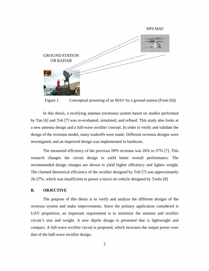
Micro-air-vehicle (MAV) propulsion is the main application of interest in this
research. MAVs are a category of unmanned air vehicles (UAVs) being developed
around the world. The definition of an MAV, according to the Defense Advanced
Research Project Agency (DARPA), is a fully functional UAV no larger than 15 cm in
length, width, and height [6]. The main reason for using wireless power transmission for
military ground-surveillance applications is to achieve unlimited duration of flight
without requiring onboard fuel supplies. One application that employs a MAV remotely
powered by a small ground station is illustrated in Figure 1.
2
NPS MAV
GROUND STATIONOR RADAR
Figure 1. Conceptual powering of an MAV by a ground station (From [6]).
In this thesis, a rectifying antenna (rectenna) system based on studies performed
by Tan [6] and Toh [7] was re-evaluated, simulated, and refined. This study also looks at
a new antenna design and a full-wave rectifier concept. In order to verify and validate the
design of the rectenna model, many tradeoffs were made. Different rectenna designs were
investigated, and an improved design was implemented in hardware.
The measured efficiency of the previous NPS rectenna was 26% to 37% [7]. This
research changes the circuit design to yield better overall performance. The
recommended design changes are shown to yield higher efficiency and lighter weight.
The claimed theoretical efficiency of the rectifier designed by Toh [7] was approximately
26-37%, which was insufficient to power a micro air vehicle designed by Tsolis [8].
B. OBJECTIVE
The purpose of this thesis is to verify and analyze the different designs of the
rectenna system and make improvements. Since the primary application considered is
UAV propulsion, an important requirement is to minimize the antenna and rectifier
circuit’s size and weight. A new dipole design is presented that is lightweight and
compact. A full-wave rectifier circuit is proposed, which increases the output power over
that of the half-wave rectifier design.

3
C. THESIS OUTLINE
This thesis is divided into six chapters. The next five are organized as follows:
Chapter II introduces the development of WPT from the early 1950s through
today. References to various WPT studies and applications are also covered in this
chapter. An overview of related thesis projects that were conducted at the Naval
Postgraduate School is presented.
Chapter III focuses on three different rectenna designs, the components of a
rectenna circuit, and evaluation of various circuit designs by using Advanced Design
System (ADS) 2009 software from Agilent Technologies. Analysis of the dipole antenna
dimensions, Schottky diode, and substrate material are covered in this chapter. Chapter
III also discusses the effects of pre- and post-rectification filtering. The design of a
rectenna with and without filters is documented, and a comparative study of the
performance of the pre-, post-, and no-filter designs analyzed.
Chapter IV discusses the impedance of the rectenna and dipole-antenna array.
Chapter V summarizes the findings of this research and presents conclusions and
recommendations for future research.

4
THIS PAGE INTENTIONALLY LEFT BLANK
5
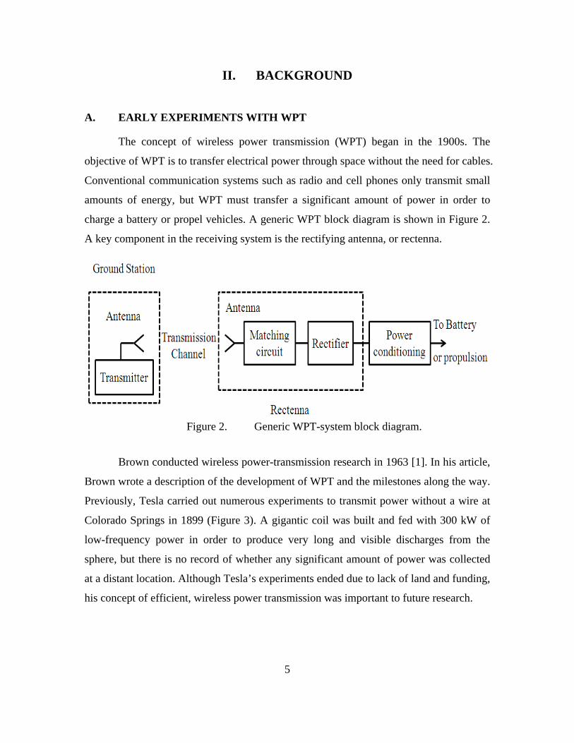
II. BACKGROUND
A. EARLY EXPERIMENTS WITH WPT
The concept of wireless power transmission (WPT) began in the 1900s. The
objective of WPT is to transfer electrical power through space without the need for cables.
Conventional communication systems such as radio and cell phones only transmit small
amounts of energy, but WPT must transfer a significant amount of power in order to
charge a battery or propel vehicles. A generic WPT block diagram is shown in Figure 2.
A key component in the receiving system is the rectifying antenna, or rectenna.
Figure 2. Generic WPT-system block diagram.
Brown conducted wireless power-transmission research in 1963 [1]. In his article,
Brown wrote a description of the development of WPT and the milestones along the way.
Previously, Tesla carried out numerous experiments to transmit power without a wire at
Colorado Springs in 1899 (Figure 3). A gigantic coil was built and fed with 300 kW of
low-frequency power in order to produce very long and visible discharges from the
sphere, but there is no record of whether any significant amount of power was collected
at a distant location. Although Tesla’s experiments ended due to lack of land and funding,
his concept of efficient, wireless power transmission was important to future research.

6
Figure 3. Experiment with radio waves for power transmission (From [1]).
In the late 1930s, a further advance in WPT occurred with the invention of the
klystron tube, which converted microwave power into dc power by using microwave
power tube at one end and dc diode tubes at the other. Advances in the microwave-cavity
magnetron led to higher efficiency for WPT applications during World War II.
In the 1950s, two advances were enabled by the invention of the amplifier tube,
which created a larger amount of transmitting power [9] to drive an electromagnetic
beam, and the focusing of electromagnetic power into a beam for high efficiencies [10].
In May 1963, Raytheon demonstrated the first microwave-power transmission system,
which converted 400 W of CW power at the transmitter to 100 W of dc power to drive a
motor.
7
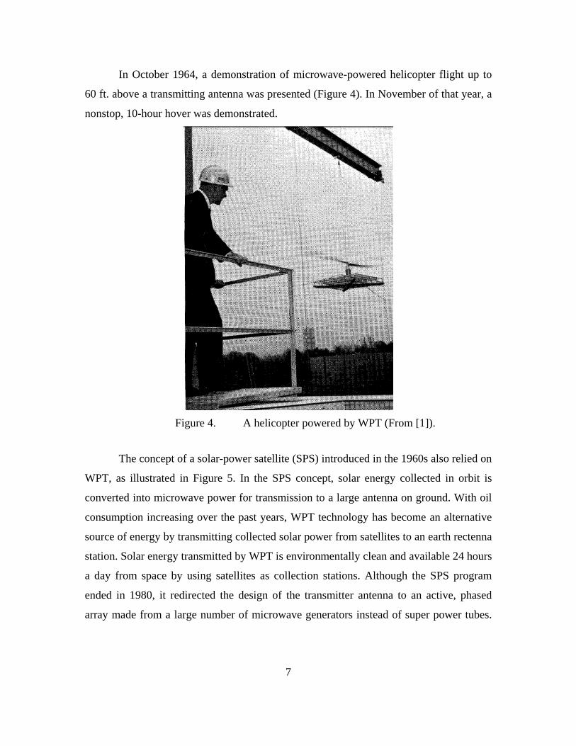
In October 1964, a demonstration of microwave-powered helicopter flight up to
60 ft. above a transmitting antenna was presented (Figure 4). In November of that year, a
nonstop, 10-hour hover was demonstrated.
Figure 4. A helicopter powered by WPT (From [1]).
The concept of a solar-power satellite (SPS) introduced in the 1960s also relied on
WPT, as illustrated in Figure 5. In the SPS concept, solar energy collected in orbit is
converted into microwave power for transmission to a large antenna on ground. With oil
consumption increasing over the past years, WPT technology has become an alternative
source of energy by transmitting collected solar power from satellites to an earth rectenna
station. Solar energy transmitted by WPT is environmentally clean and available 24 hours
a day from space by using satellites as collection stations. Although the SPS program
ended in 1980, it redirected the design of the transmitter antenna to an active, phased
array made from a large number of microwave generators instead of super power tubes.
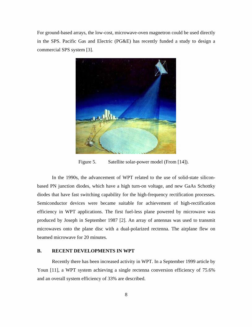
8
For ground-based arrays, the low-cost, microwave-oven magnetron could be used directly
in the SPS. Pacific Gas and Electric (PG&E) has recently funded a study to design a
commercial SPS system [3].
Figure 5. Satellite solar-power model (From [14]).
In the 1990s, the advancement of WPT related to the use of solid-state silicon-
based PN junction diodes, which have a high turn-on voltage, and new GaAs Schottky
diodes that have fast switching capability for the high-frequency rectification processes.
Semiconductor devices were became suitable for achievement of high-rectification
efficiency in WPT applications. The first fuel-less plane powered by microwave was
produced by Joseph in September 1987 [2]. An array of antennas was used to transmit
microwaves onto the plane disc with a dual-polarized rectenna. The airplane flew on
beamed microwave for 20 minutes.
B. RECENT DEVELOPMENTS IN WPT
Recently there has been increased activity in WPT. In a September 1999 article by
Youn [11], a WPT system achieving a single rectenna conversion efficiency of 75.6%
and an overall system efficiency of 33% are described.
9
Hagerty [12] proposed an array of 64 circularly polarized spiral elements and used
a broadband-antenna array to convert more microwave power into dc power. The
achievement of 20% efficiency over a frequency range of 2–18 GHz was reported.
A December 2002 survey article on space solar-power (SSP) program research
was written by McSpadden [13]. McSpadden gave insight on achieving practical SSP and
emphasized three critical components: the transmitter, beam control, and rectennas.
Although it was acknowledged that the technology was immature, a strategic roadmap
was highlighted for future investigation.
In [14], Goel proposed that a solar-power satellite could be placed in halo orbit to
be fixed over the earth’s midnight as the earth rotates. The proposed orbit, known as the
trans-earth Lagrange point, obviates the need for a rotating joint between the solar array
and microwave transmitter, making a simpler design possible.
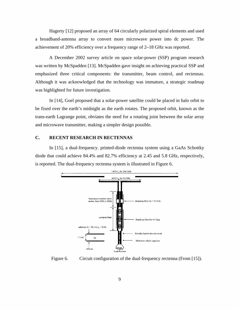
C. RECENT RESEARCH IN RECTENNAS
In [15], a dual-frequency. printed-diode rectenna system using a GaAs Schottky
diode that could achieve 84.4% and 82.7% efficiency at 2.45 and 5.8 GHz, respectively,
is reported. The dual-frequency rectenna system is illustrated in Figure 6.
Figure 6. Circuit configuration of the dual-frequency rectenna (From [15]).
10
Reference [16] by Strassner contains an article on a 5.8 GHz, circularly polarized
rectenna design and array. Strassner demonstrated the feasibility of a rectenna array
scaled 3 feet wide by 2 feet long and 4 inches tall, with an efficiency of 82% and output
power of 7.6 W.
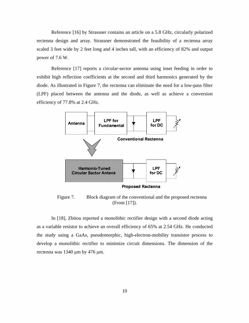
Reference [17] reports a circular-sector antenna using inset feeding in order to
exhibit high reflection coefficients at the second and third harmonics generated by the
diode. As illustrated in Figure 7, the rectenna can eliminate the need for a low-pass filter
(LPF) placed between the antenna and the diode, as well as achieve a conversion
efficiency of 77.8% at 2.4 GHz.
Figure 7. Block diagram of the conventional and the proposed rectenna (From [17]).
In [18], Zbitou reported a monolithic rectifier design with a second diode acting
as a variable resistor to achieve an overall efficiency of 65% at 2.54 GHz. He conducted
the study using a GaAs, pseudomorphic, high-electron-mobility transistor process to
develop a monolithic rectifier to minimize circuit dimensions. The dimension of the
rectenna was 1340 μm by 476 μm.
11
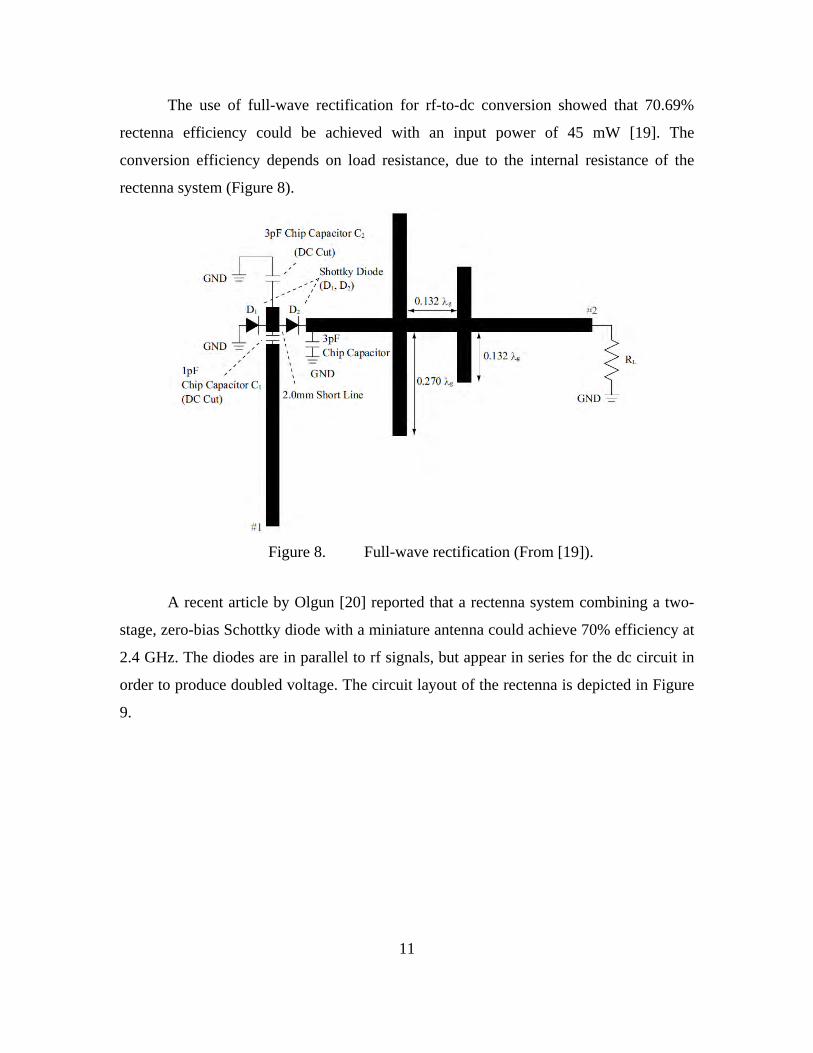
The use of full-wave rectification for rf-to-dc conversion showed that 70.69%
rectenna efficiency could be achieved with an input power of 45 mW [19]. The
conversion efficiency depends on load resistance, due to the internal resistance of the
rectenna system (Figure 8).
Figure 8. Full-wave rectification (From [19]).
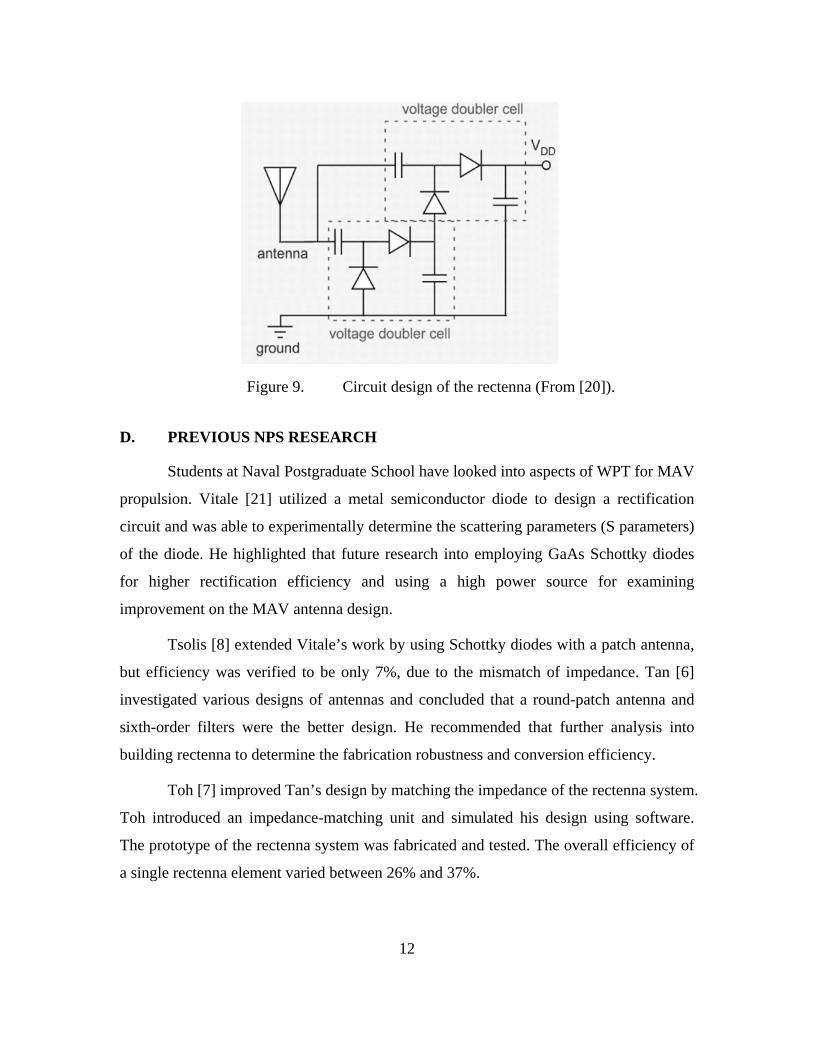
A recent article by Olgun [20] reported that a rectenna system combining a two-
stage, zero-bias Schottky diode with a miniature antenna could achieve 70% efficiency at
2.4 GHz. The diodes are in parallel to rf signals, but appear in series for the dc circuit in
order to produce doubled voltage. The circuit layout of the rectenna is depicted in Figure
9.
12
Figure 9. Circuit design of the rectenna (From [20]).
D. PREVIOUS NPS RESEARCH
Students at Naval Postgraduate School have looked into aspects of WPT for MAV
propulsion. Vitale [21] utilized a metal semiconductor diode to design a rectification
circuit and was able to experimentally determine the scattering parameters (S parameters)
of the diode. He highlighted that future research into employing GaAs Schottky diodes
for higher rectification efficiency and using a high power source for examining
improvement on the MAV antenna design.
Tsolis [8] extended Vitale’s work by using Schottky diodes with a patch antenna,
but efficiency was verified to be only 7%, due to the mismatch of impedance. Tan [6]
investigated various designs of antennas and concluded that a round-patch antenna and
sixth-order filters were the better design. He recommended that further analysis into
building rectenna to determine the fabrication robustness and conversion efficiency.
Toh [7] improved Tan’s design by matching the impedance of the rectenna system.
Toh introduced an impedance-matching unit and simulated his design using software.
The prototype of the rectenna system was fabricated and tested. The overall efficiency of
a single rectenna element varied between 26% and 37%.

13
E. SUMMARY
In this chapter, the major milestones in the development of WPT were highlighted
and a brief history of WPT was covered. Much research has been conducted to determine
the feasibility of implementing WPT and its applications, which range from miniaturized
versions of remotely powered vehicles to large-scale systems. In the next chapter,
rectenna design is addressed in detail.
Equation Chapter 3 Section 1

14
THIS PAGE INTENTIONALLY LEFT BLANK
15
III. RECTENNA DESIGN
A. DISCUSSION OF RECTENNA DESIGN
1. General Rectenna Design
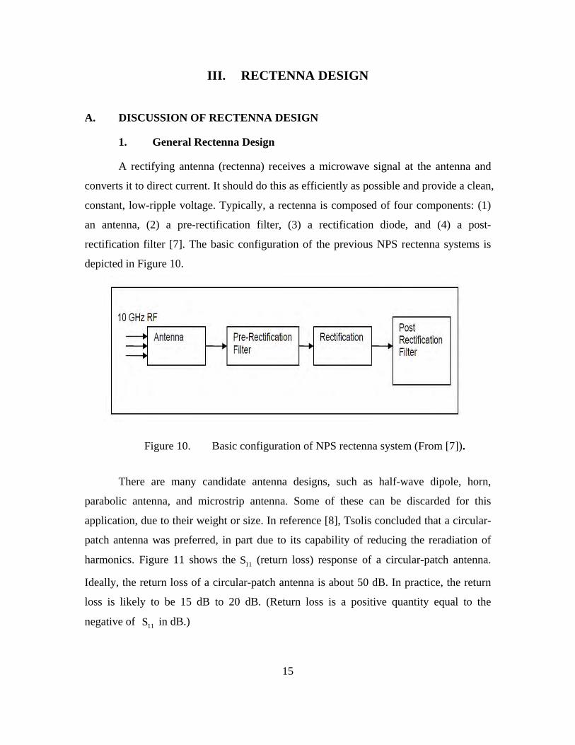
A rectifying antenna (rectenna) receives a microwave signal at the antenna and
converts it to direct current. It should do this as efficiently as possible and provide a clean,
constant, low-ripple voltage. Typically, a rectenna is composed of four components: (1)
an antenna, (2) a pre-rectification filter, (3) a rectification diode, and (4) a post-
rectification filter [7]. The basic configuration of the previous NPS rectenna systems is
depicted in Figure 10.
Figure 10. Basic configuration of NPS rectenna system (From [7]).
There are many candidate antenna designs, such as half-wave dipole, horn,
parabolic antenna, and microstrip antenna. Some of these can be discarded for this
application, due to their weight or size. In reference [8], Tsolis concluded that a circular-
patch antenna was preferred, in part due to its capability of reducing the reradiation of
harmonics. Figure 11 shows the 11S (return loss) response of a circular-patch antenna.
Ideally, the return loss of a circular-patch antenna is about 50 dB. In practice, the return
loss is likely to be 15 dB to 20 dB. (Return loss is a positive quantity equal to the
negative of 11S in dB.)
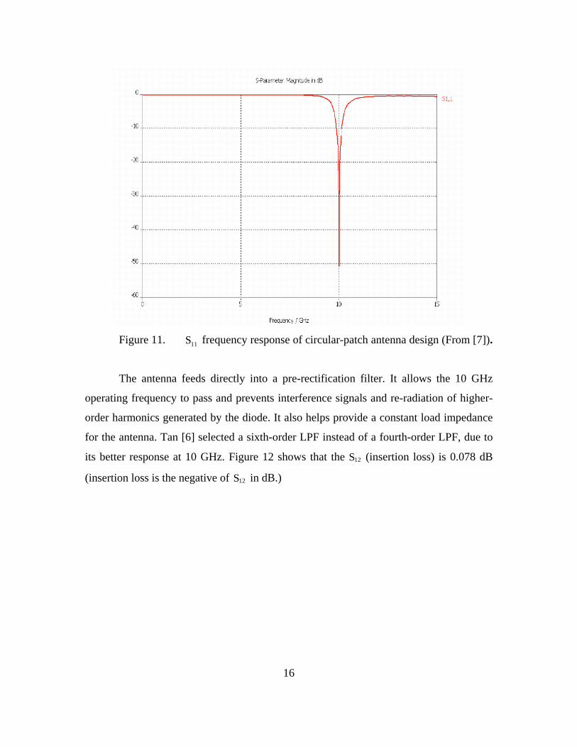
16
Figure 11. 11S frequency response of circular-patch antenna design (From [7]).
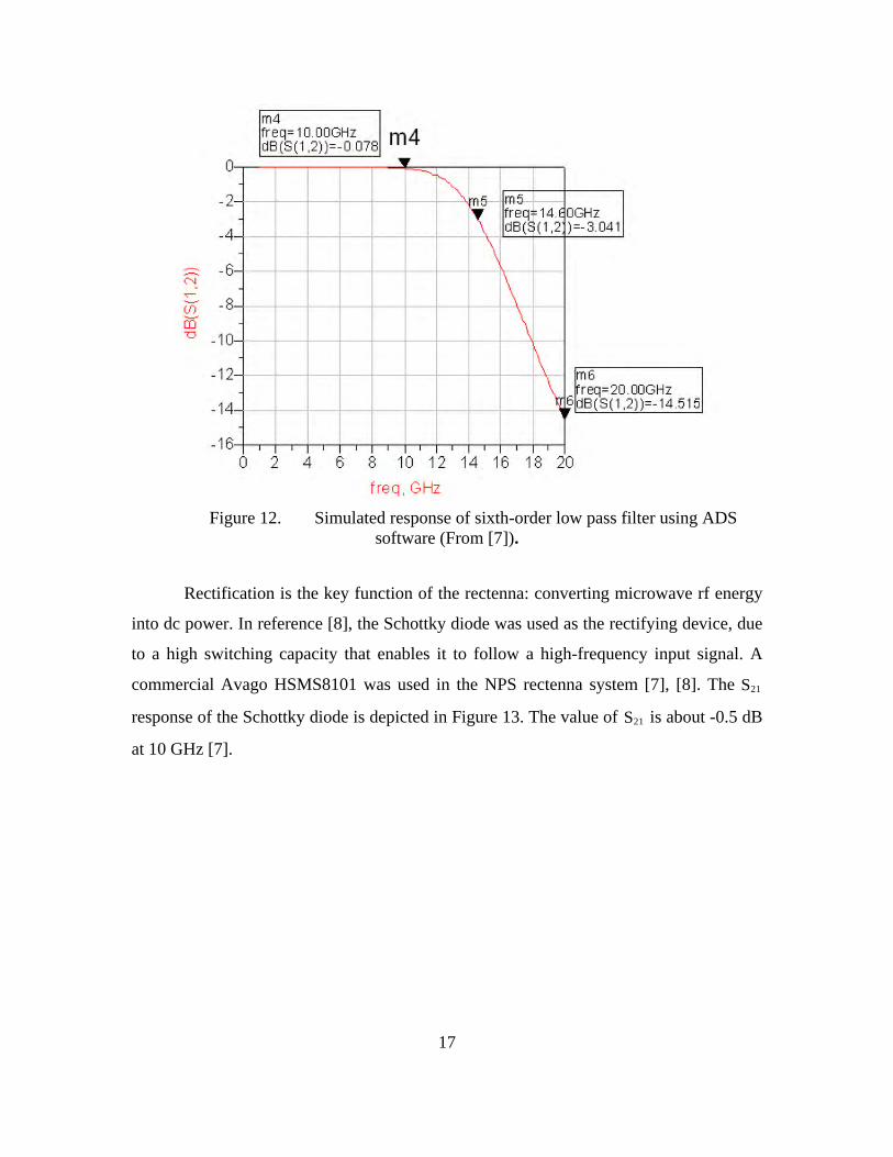
The antenna feeds directly into a pre-rectification filter. It allows the 10 GHz
operating frequency to pass and prevents interference signals and re-radiation of higher-
order harmonics generated by the diode. It also helps provide a constant load impedance
for the antenna. Tan [6] selected a sixth-order LPF instead of a fourth-order LPF, due to
its better response at 10 GHz. Figure 12 shows that the 12S (insertion loss) is 0.078 dB
(insertion loss is the negative of 12S in dB.)
17
Figure 12. Simulated response of sixth-order low pass filter using ADS software (From [7]).
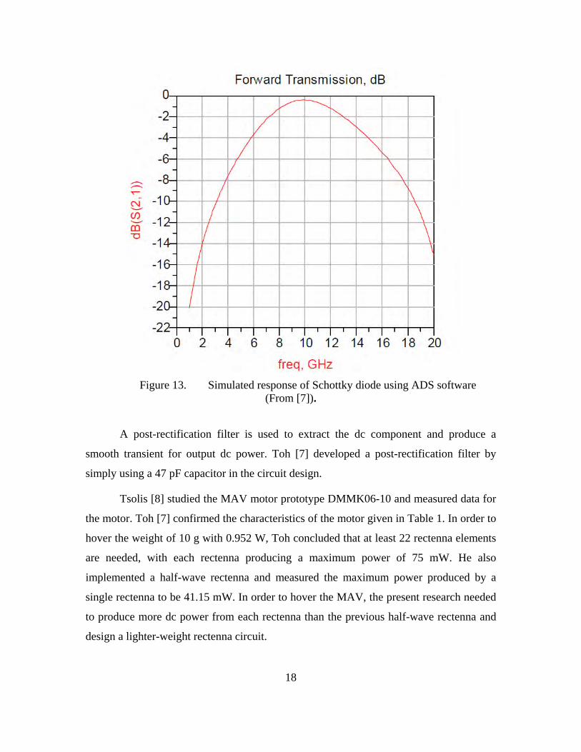
Rectification is the key function of the rectenna: converting microwave rf energy
into dc power. In reference [8], the Schottky diode was used as the rectifying device, due
to a high switching capacity that enables it to follow a high-frequency input signal. A
commercial Avago HSMS8101 was used in the NPS rectenna system [7], [8]. The 21S
response of the Schottky diode is depicted in Figure 13. The value of 21S is about -0.5 dB
at 10 GHz [7].
18
Figure 13. Simulated response of Schottky diode using ADS software (From [7]).
A post-rectification filter is used to extract the dc component and produce a
smooth transient for output dc power. Toh [7] developed a post-rectification filter by
simply using a 47 pF capacitor in the circuit design.
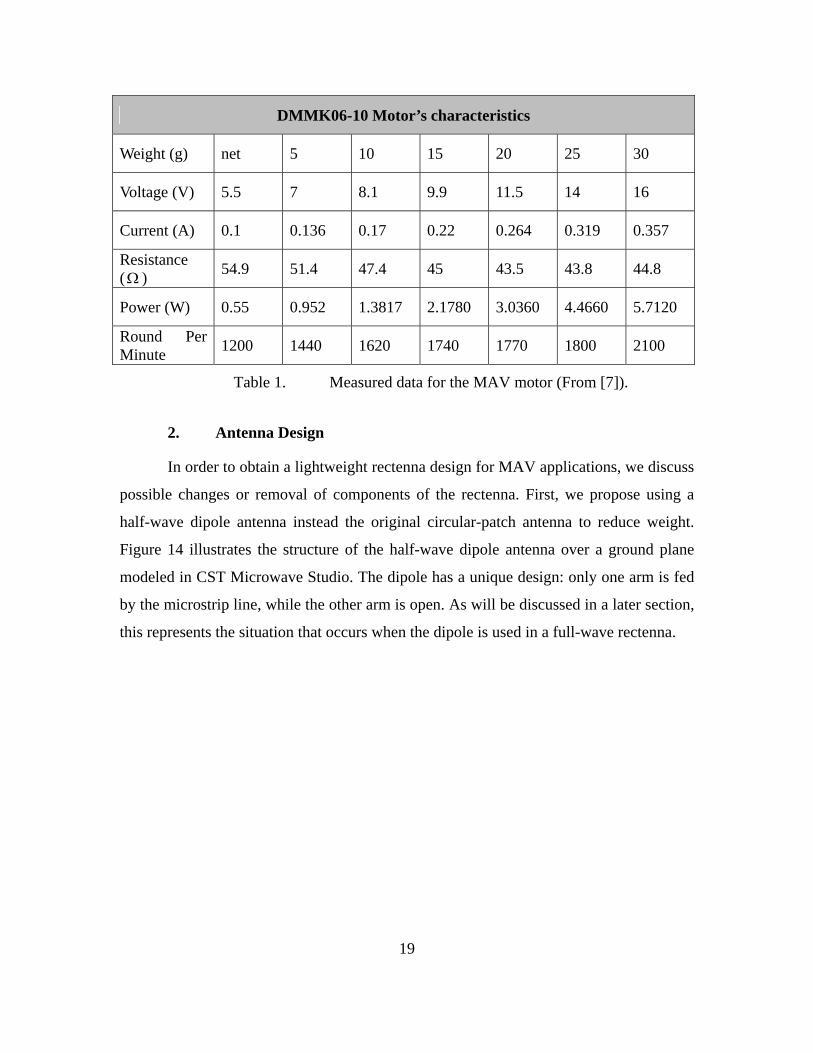
Tsolis [8] studied the MAV motor prototype DMMK06-10 and measured data for
the motor. Toh [7] confirmed the characteristics of the motor given in Table 1. In order to
hover the weight of 10 g with 0.952 W, Toh concluded that at least 22 rectenna elements
are needed, with each rectenna producing a maximum power of 75 mW. He also
implemented a half-wave rectenna and measured the maximum power produced by a
single rectenna to be 41.15 mW. In order to hover the MAV, the present research needed
to produce more dc power from each rectenna than the previous half-wave rectenna and
design a lighter-weight rectenna circuit.
19
DMMK06-10 Motor’s characteristics
Weight (g) net 5 10 15 20 25 30
Voltage (V) 5.5 7 8.1 9.9 11.5 14 16
Current (A) 0.1 0.136 0.17 0.22 0.264 0.319 0.357
Resistance ( )
54.9 51.4 47.4 45 43.5 43.8 44.8
Power (W) 0.55 0.952 1.3817 2.1780 3.0360 4.4660 5.7120
Round Per Minute
1200 1440 1620 1740 1770 1800 2100
Table 1. Measured data for the MAV motor (From [7]).
2. Antenna Design
In order to obtain a lightweight rectenna design for MAV applications, we discuss
possible changes or removal of components of the rectenna. First, we propose using a
half-wave dipole antenna instead the original circular-patch antenna to reduce weight.
Figure 14 illustrates the structure of the half-wave dipole antenna over a ground plane
modeled in CST Microwave Studio. The dipole has a unique design: only one arm is fed
by the microstrip line, while the other arm is open. As will be discussed in a later section,
this represents the situation that occurs when the dipole is used in a full-wave rectenna.

20
Figure 14. Two views of the half-wave, dipole-antenna structure.
Table 2 lists the design specifications for the data in Figure 15 through 17.
21
Half-wave dipole’s specifications
Dipole wire radius (r) 0.25 Gap width (g) 1.5
Substrate height (t) 0.508 Dipole height above ground (h) 9
50 ohm line width (d) 1.6829 Sample width (X) 25
Dipole length (L) 25 Sample length (Y) 35
Table 2. Design specifications for the half-wave dipole antenna.
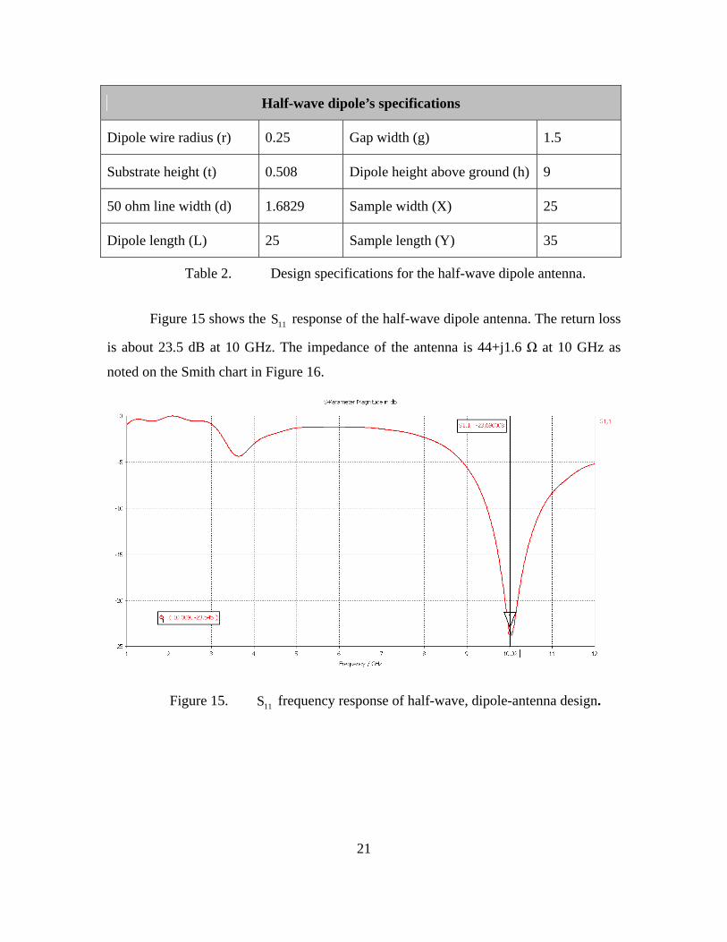
Figure 15 shows the 11S response of the half-wave dipole antenna. The return loss
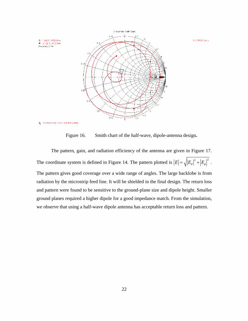
is about 23.5 dB at 10 GHz. The impedance of the antenna is 44+j1.6 Ω at 10 GHz as
noted on the Smith chart in Figure 16.
Figure 15. 11S frequency response of half-wave, dipole-antenna design.
22
Figure 16. Smith chart of the half-wave, dipole-antenna design.
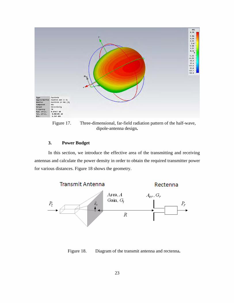
The pattern, gain, and radiation efficiency of the antenna are given in Figure 17.
The coordinate system is defined in Figure 14. The pattern plotted is 22
E E E .
The pattern gives good coverage over a wide range of angles. The large backlobe is from
radiation by the microstrip feed line. It will be shielded in the final design. The return loss
and pattern were found to be sensitive to the ground-plane size and dipole height. Smaller
ground planes required a higher dipole for a good impedance match. From the simulation,
we observe that using a half-wave dipole antenna has acceptable return loss and pattern.
23
Figure 17. Three-dimensional, far-field radiation pattern of the half-wave, dipole-antenna design.
3. Power Budget
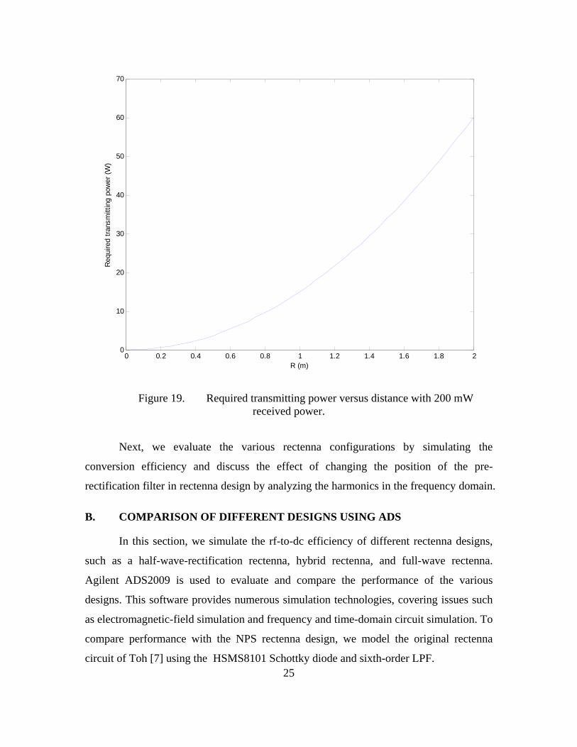
In this section, we introduce the effective area of the transmitting and receiving
antennas and calculate the power density in order to obtain the required transmitter power
for various distances. Figure 18 shows the geometry.
Figure 18. Diagram of the transmit antenna and rectenna.

24
The effective area of the dipole antenna over a perfect ground plane is calculated
using:
2
4r
er
GA
(3.1)
where rG is the gain of the dipole antenna and is the wavelength at 10 GHz. From
Figure 17, the gain is 6.16 dB = 4.13. Using Eq. (3.1), the effective area of the dipole
antenna is 42.96 10 2m . The power density iW transmitted by the horn antenna at
distance R can be expressed as
2
2 2 2 2
4
4 4
ett
t t t eti
APPG P A
WR R R
(3.2)
where tP is the transmitted power, etA is the effective area of the horn antenna, and R is
the distance between transmitting and receiving antennas. The effective area of the horn
antenna is the physical area ( A ) times the efficiency, te . Assuming horn dimensions of 3
inches by 4 inches and an efficiency of 0.7, 0.0054etA 2m , the power rP received by
dipole antenna can be expressed as
2 2
.t et err i er
P A AP W A
R (3.3)
Using Equation (3.3), the required transmitting power versus the distance between
transmitting and receiving antennas to obtain 200 mW of received power is given in
Figure 19. From Figure 19, the transmitted power is 1.35 W for the distance of 30 cm,
and the received power will be 200 mW. This analysis assumes the distance R is in the
far field of the horn antenna.
25
0 0.2 0.4 0.6 0.8 1 1.2 1.4 1.6 1.8 20
10
20
30
40
50
60
70
R (m)
Req
uire
d tr
ansm
ittin
g po
wer
(W
)
Figure 19. Required transmitting power versus distance with 200 mW received power.
Next, we evaluate the various rectenna configurations by simulating the
conversion efficiency and discuss the effect of changing the position of the pre-
rectification filter in rectenna design by analyzing the harmonics in the frequency domain.
B. COMPARISON OF DIFFERENT DESIGNS USING ADS
In this section, we simulate the rf-to-dc efficiency of different rectenna designs,
such as a half-wave-rectification rectenna, hybrid rectenna, and full-wave rectenna.
Agilent ADS2009 is used to evaluate and compare the performance of the various
designs. This software provides numerous simulation technologies, covering issues such
as electromagnetic-field simulation and frequency and time-domain circuit simulation. To
compare performance with the NPS rectenna design, we model the original rectenna
circuit of Toh [7] using the HSMS8101 Schottky diode and sixth-order LPF.
26
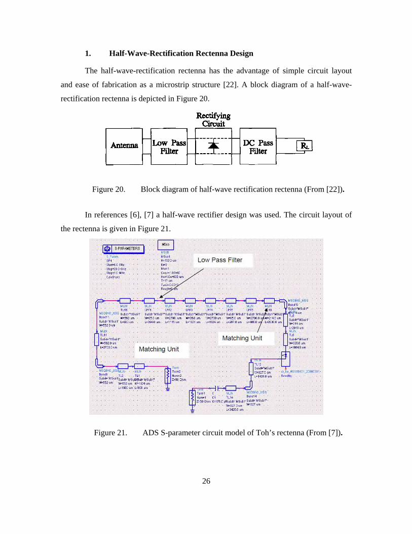
1. Half-Wave-Rectification Rectenna Design
The half-wave-rectification rectenna has the advantage of simple circuit layout
and ease of fabrication as a microstrip structure [22]. A block diagram of a half-wave-
rectification rectenna is depicted in Figure 20.
Figure 20. Block diagram of half-wave rectification rectenna (From [22]).
In references [6], [7] a half-wave rectifier design was used. The circuit layout of
the rectenna is given in Figure 21.
Figure 21. ADS S-parameter circuit model of Toh’s rectenna (From [7]).
27
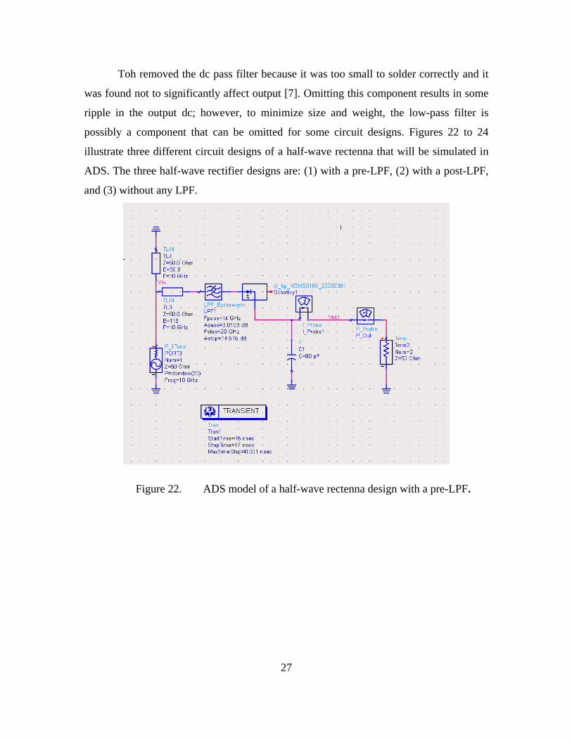
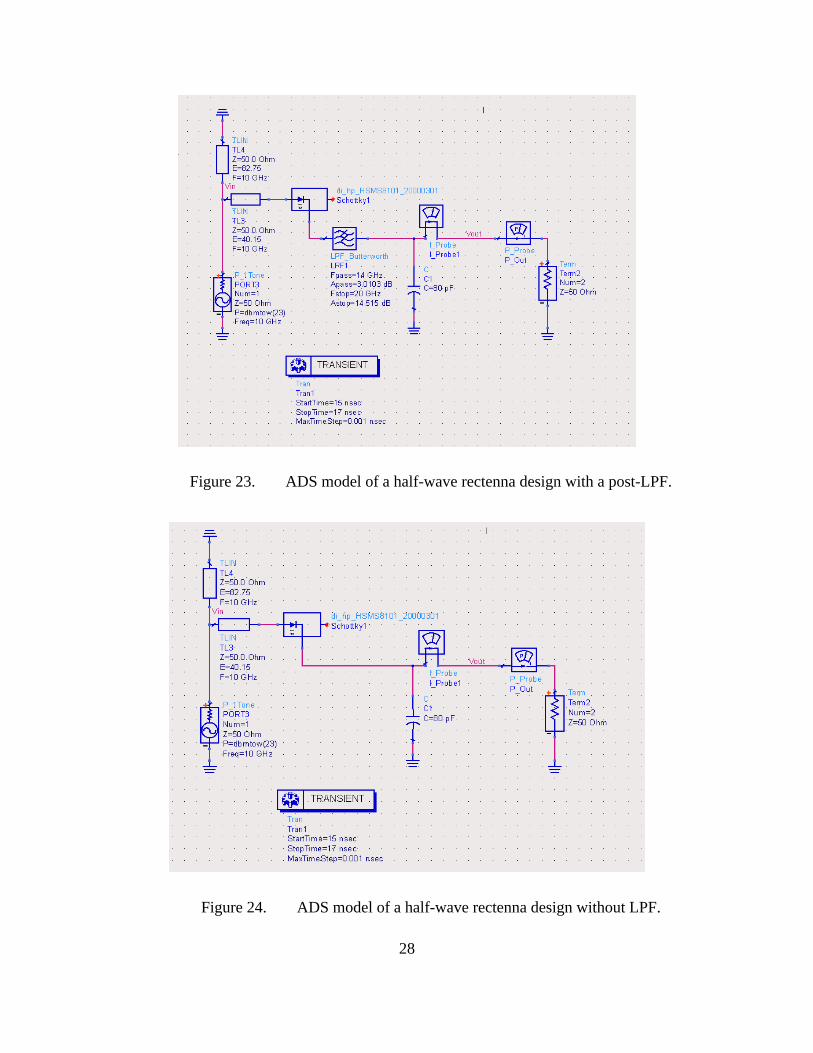
Toh removed the dc pass filter because it was too small to solder correctly and it
was found not to significantly affect output [7]. Omitting this component results in some
ripple in the output dc; however, to minimize size and weight, the low-pass filter is
possibly a component that can be omitted for some circuit designs. Figures 22 to 24
illustrate three different circuit designs of a half-wave rectenna that will be simulated in
ADS. The three half-wave rectifier designs are: (1) with a pre-LPF, (2) with a post-LPF,
and (3) without any LPF.
Figure 22. ADS model of a half-wave rectenna design with a pre-LPF.
28
Figure 23. ADS model of a half-wave rectenna design with a post-LPF.
Figure 24. ADS model of a half-wave rectenna design without LPF.

29
All three designs utilize a capacitor after the diode. In reference [21], Vitale noted
that the output voltage when the diode is not conducting is compensated for by the
discharge of the filter capacitor. It can be expressed as
Lt R Cout PV t V e (3.4)
where PV is the peak voltage of the rectified signal, LR is the load resistance, and C is
the filter capacitance. For LR C T , the exponential can be approximated by
1L
TR C
and the minimum output voltage can be expressed as
min 1PL
TV V
R C
(3.5)
where T is a full period of the input sinusoid. He also determined that the output dc
voltage outV is approximated by the average voltage between the peak voltage and the
minimum output voltage
1
1 .2out P
L
V VfR C
(3.6)
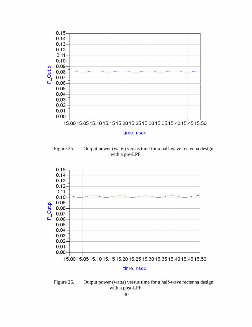
Figures 25 to 27 illustrate the output dc power produced by the three different circuit
designs of a half-wave rectenna that were simulated in ADS.
30
Figure 25. Output power (watts) versus time for a half-wave rectenna design with a pre-LPF.
Figure 26. Output power (watts) versus time for a half-wave rectenna design with a post-LPF.
31
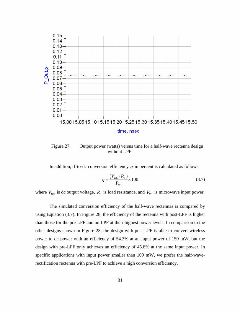
Figure 27. Output power (watts) versus time for a half-wave rectenna design without LPF.
In addition, rf-to-dc conversion efficiency in percent is calculated as follows:
100DC L
RF
V R
P (3.7)
where DCV is dc output voltage, LR
is load resistance, and RFP is microwave input power.
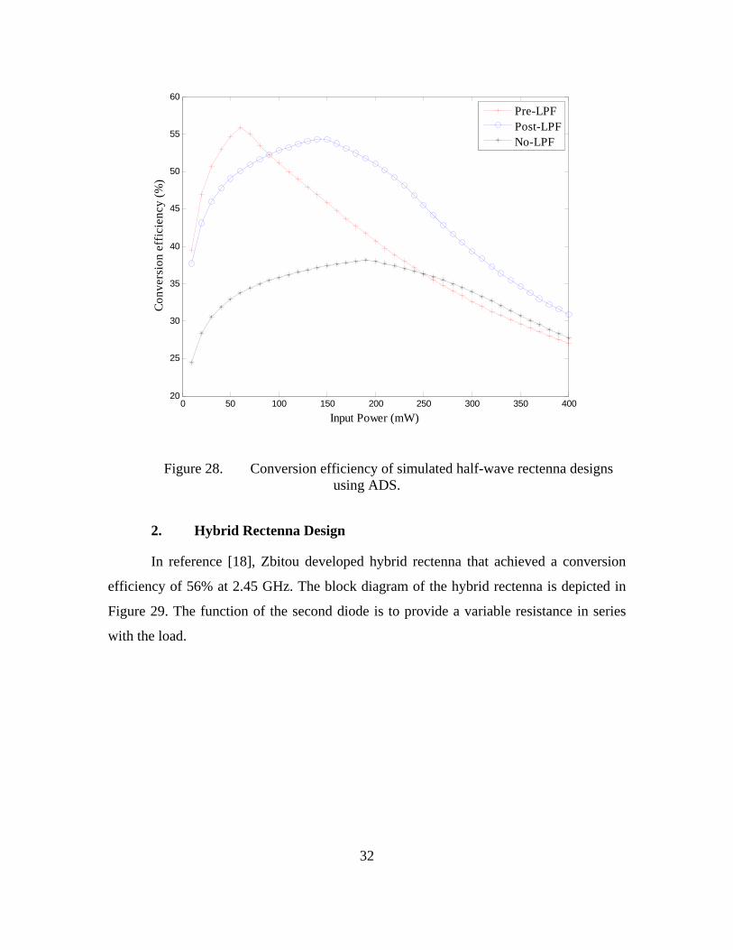
The simulated conversion efficiency of the half-wave rectennas is compared by
using Equation (3.7). In Figure 28, the efficiency of the rectenna with post-LPF is higher
than those for the pre-LPF and no LPF at their highest power levels. In comparison to the
other designs shown in Figure 28, the design with post-LPF is able to convert wireless
power to dc power with an efficiency of 54.3% at an input power of 150 mW, but the
design with pre-LPF only achieves an efficiency of 45.8% at the same input power. In
specific applications with input power smaller than 100 mW, we prefer the half-wave-
rectification rectenna with pre-LPF to achieve a high conversion efficiency.
32
0 50 100 150 200 250 300 350 40020
25
30
35
40
45
50
55
60
Input Power (mW)
Con
vers
ion
effi
cien
cy (
%)
Pre-LPFPost-LPFNo-LPF
Figure 28. Conversion efficiency of simulated half-wave rectenna designs using ADS.
2. Hybrid Rectenna Design
In reference [18], Zbitou developed hybrid rectenna that achieved a conversion
efficiency of 56% at 2.45 GHz. The block diagram of the hybrid rectenna is depicted in
Figure 29. The function of the second diode is to provide a variable resistance in series
with the load.
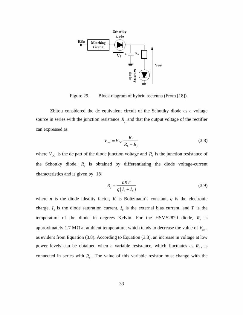
33
Figure 29. Block diagram of hybrid rectenna (From [18]).
Zbitou considered the dc equivalent circuit of the Schottky diode as a voltage
source in series with the junction resistance jR and that the output voltage of the rectifier
can expressed as
Lout DC
L j
RV V
R R
(3.8)
where DCV is the dc part of the diode junction voltage and jR is the junction resistance of
the Schottky diode. jR is obtained by differentiating the diode voltage-current
characteristics and is given by [18]
j
s b
nKTR
q I I
(3.9)
where n is the diode ideality factor, K is Boltzmann’s constant, q is the electronic
charge, sI is the diode saturation current, bI is the external bias current, and T is the
temperature of the diode in degrees Kelvin. For the HSMS2820 diode, jR is
approximately 1.7 M at ambient temperature, which tends to decrease the value of outV ,
as evident from Equation (3.8). According to Equation (3.8), an increase in voltage at low
power levels can be obtained when a variable resistance, which fluctuates as jR , is
connected in series with LR . The value of this variable resistor must change with the
34
rectified current. Thus, Zbitou employed a technique using the same Schottky diode in
series with LR , in the dc portion of the rectifier, to act as a variable resistor (due to its
current dependence in the junction resistance).
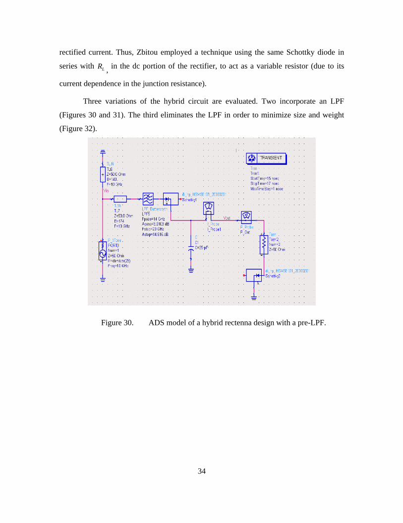
Three variations of the hybrid circuit are evaluated. Two incorporate an LPF
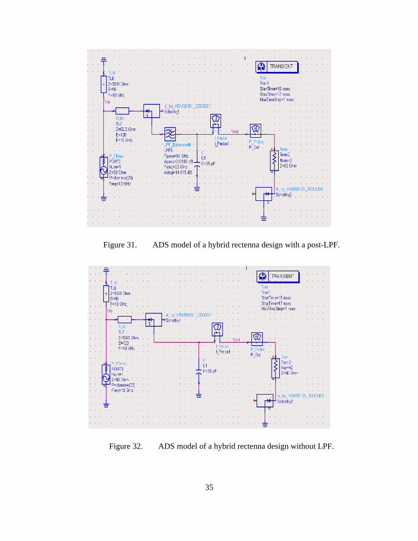
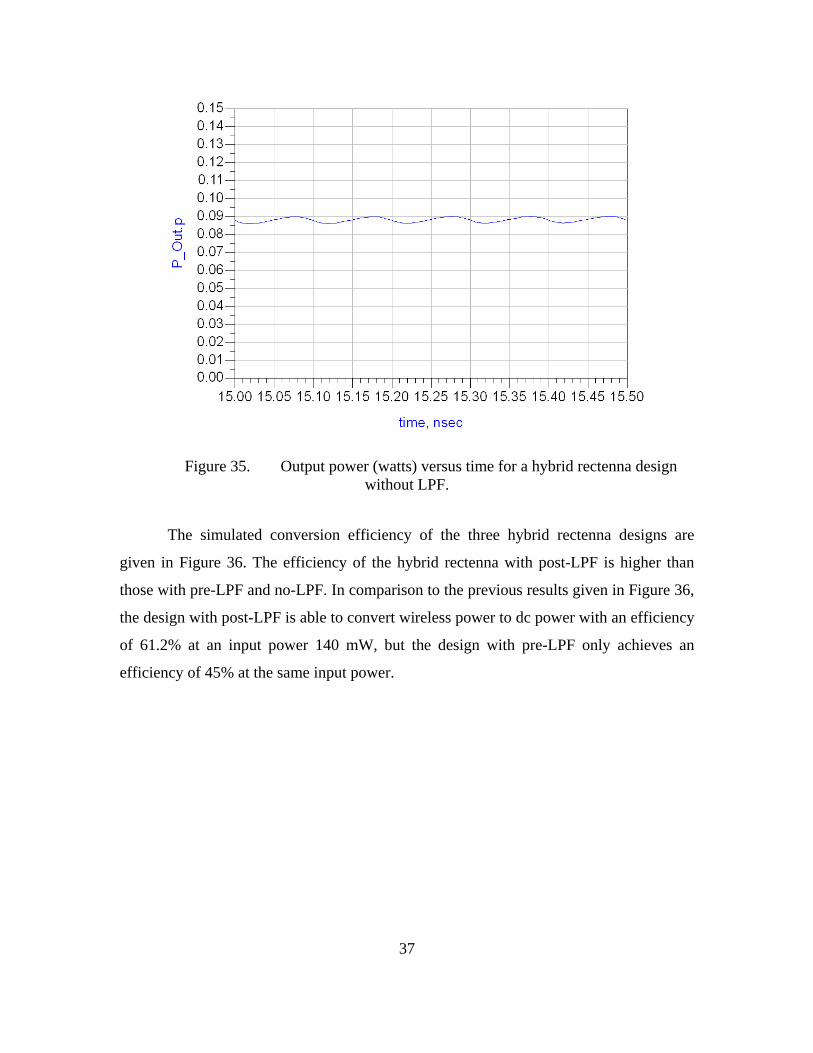
(Figures 30 and 31). The third eliminates the LPF in order to minimize size and weight
(Figure 32).
Figure 30. ADS model of a hybrid rectenna design with a pre-LPF.
35
Figure 31. ADS model of a hybrid rectenna design with a post-LPF.
Figure 32. ADS model of a hybrid rectenna design without LPF.

36
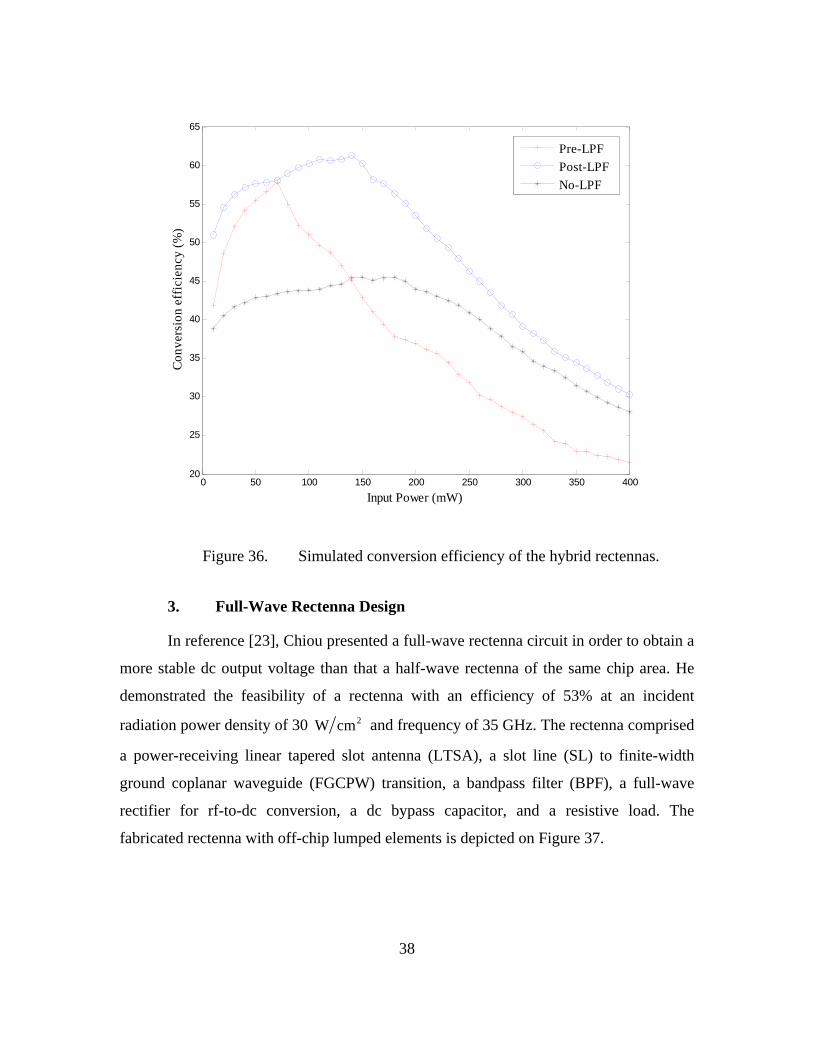
Figures 33 to 35 illustrate the output dc power produced by three different circuit
designs of hybrid rectenna that were simulated in ADS.
Figure 33. Output power (watts) versus time for a hybrid rectenna design with a pre-LPF.
Figure 34. Output power (watts) versus time for a hybrid rectenna design with a post-LPF.
37
Figure 35. Output power (watts) versus time for a hybrid rectenna design without LPF.
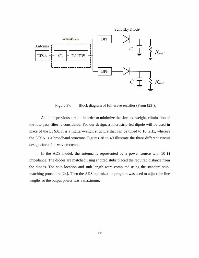
The simulated conversion efficiency of the three hybrid rectenna designs are
given in Figure 36. The efficiency of the hybrid rectenna with post-LPF is higher than
those with pre-LPF and no-LPF. In comparison to the previous results given in Figure 36,
the design with post-LPF is able to convert wireless power to dc power with an efficiency
of 61.2% at an input power 140 mW, but the design with pre-LPF only achieves an
efficiency of 45% at the same input power.
38
0 50 100 150 200 250 300 350 40020
25
30
35
40
45
50
55
60
65
Input Power (mW)
Con
vers
ion
effi
cien
cy (
%)
Pre-LPF
Post-LPF
No-LPF
Figure 36. Simulated conversion efficiency of the hybrid rectennas.
3. Full-Wave Rectenna Design
In reference [23], Chiou presented a full-wave rectenna circuit in order to obtain a
more stable dc output voltage than that a half-wave rectenna of the same chip area. He
demonstrated the feasibility of a rectenna with an efficiency of 53% at an incident
radiation power density of 30 2W cm and frequency of 35 GHz. The rectenna comprised
a power-receiving linear tapered slot antenna (LTSA), a slot line (SL) to finite-width
ground coplanar waveguide (FGCPW) transition, a bandpass filter (BPF), a full-wave
rectifier for rf-to-dc conversion, a dc bypass capacitor, and a resistive load. The
fabricated rectenna with off-chip lumped elements is depicted on Figure 37.
39
Figure 37. Block diagram of full-wave rectifier (From [23]).
As in the previous circuit, in order to minimize the size and weight, elimination of
the low-pass filter is considered. For our design, a microstrip-fed dipole will be used in
place of the LTSA. It is a lighter-weight structure that can be tuned to 10 GHz, whereas
the LTSA is a broadband structure. Figures 38 to 40 illustrate the three different circuit
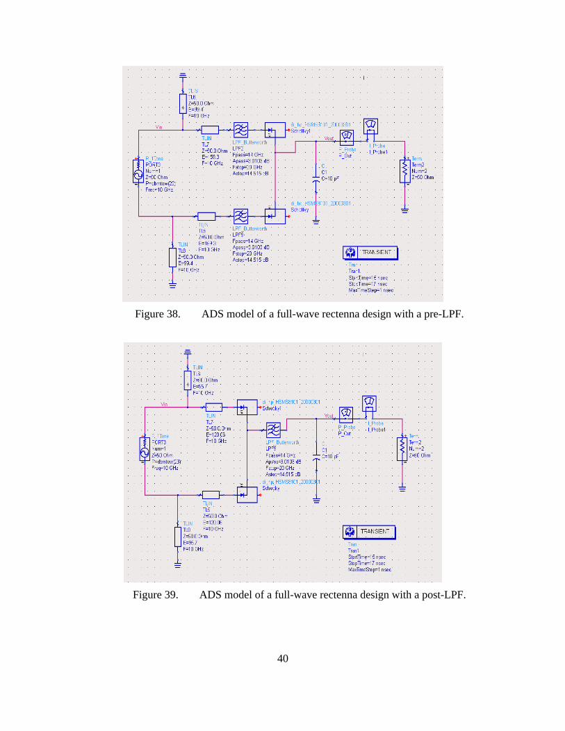
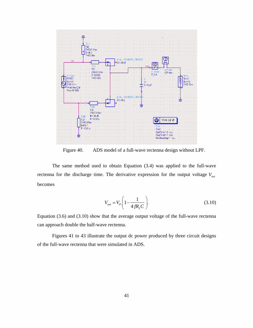
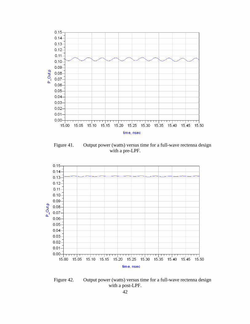
designs for a full-wave rectenna.
In the ADS model, the antenna is represented by a power source with 50 Ω
impedance. The diodes are matched using shorted stubs placed the required distance from
the diodes. The stub location and stub length were computed using the standard stub-
matching procedure [24]. Then the ADS optimization program was used to adjust the line
lengths so the output power was a maximum.
40
Figure 38. ADS model of a full-wave rectenna design with a pre-LPF.
Figure 39. ADS model of a full-wave rectenna design with a post-LPF.
41
Figure 40. ADS model of a full-wave rectenna design without LPF.
The same method used to obtain Equation (3.4) was applied to the full-wave
rectenna for the discharge time. The derivative expression for the output voltage outV
becomes
1
1 .4out P
L
V VfR C
(3.10)
Equation (3.6) and (3.10) show that the average output voltage of the full-wave rectenna
can approach double the half-wave rectenna.
Figures 41 to 43 illustrate the output dc power produced by three circuit designs
of the full-wave rectenna that were simulated in ADS.
42
Figure 41. Output power (watts) versus time for a full-wave rectenna design with a pre-LPF.
Figure 42. Output power (watts) versus time for a full-wave rectenna design with a post-LPF.
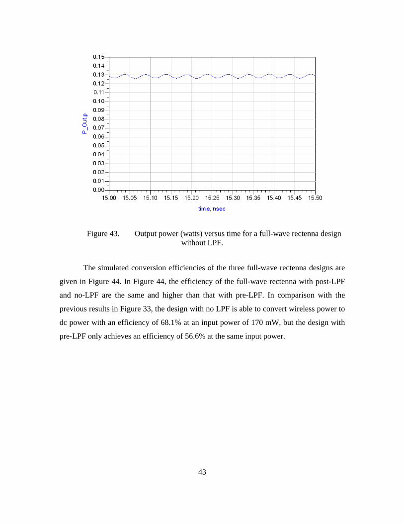
43
Figure 43. Output power (watts) versus time for a full-wave rectenna design without LPF.
The simulated conversion efficiencies of the three full-wave rectenna designs are
given in Figure 44. In Figure 44, the efficiency of the full-wave rectenna with post-LPF
and no-LPF are the same and higher than that with pre-LPF. In comparison with the
previous results in Figure 33, the design with no LPF is able to convert wireless power to
dc power with an efficiency of 68.1% at an input power of 170 mW, but the design with
pre-LPF only achieves an efficiency of 56.6% at the same input power.
44
0 50 100 150 200 250 300 350 40030
35
40
45
50
55
60
65
70
Input Power (mW)
Con
vers
ion
effi
cien
cy (
%)
Pre-LPFPost-LPFNo-LPF
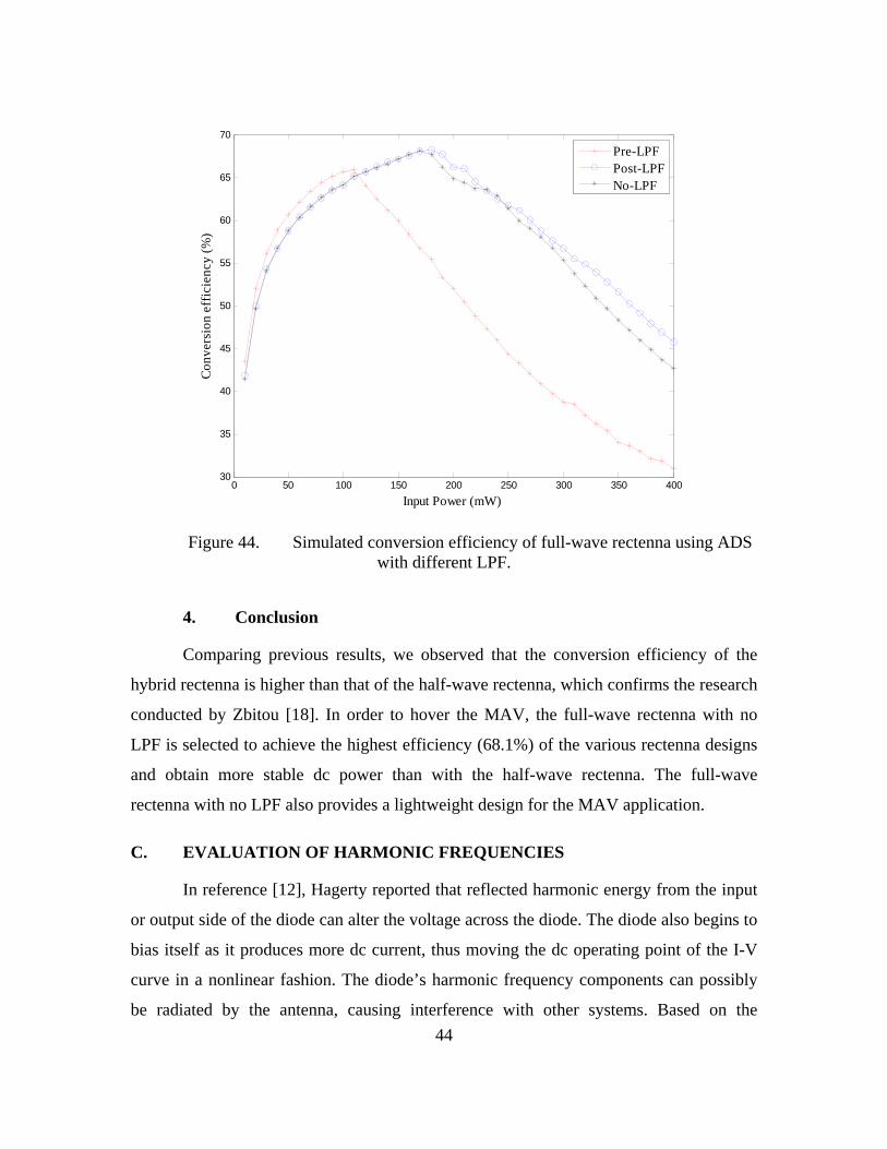
Figure 44. Simulated conversion efficiency of full-wave rectenna using ADS with different LPF.
4. Conclusion
Comparing previous results, we observed that the conversion efficiency of the
hybrid rectenna is higher than that of the half-wave rectenna, which confirms the research
conducted by Zbitou [18]. In order to hover the MAV, the full-wave rectenna with no
LPF is selected to achieve the highest efficiency (68.1%) of the various rectenna designs
and obtain more stable dc power than with the half-wave rectenna. The full-wave
rectenna with no LPF also provides a lightweight design for the MAV application.
C. EVALUATION OF HARMONIC FREQUENCIES
In reference [12], Hagerty reported that reflected harmonic energy from the input
or output side of the diode can alter the voltage across the diode. The diode also begins to
bias itself as it produces more dc current, thus moving the dc operating point of the I-V
curve in a nonlinear fashion. The diode’s harmonic frequency components can possibly
be radiated by the antenna, causing interference with other systems. Based on the
45
properties of the diode at microwave frequencies, we simulate and analyze the radiated
harmonics and dc power of different rectenna designs for an input microwave power at
10 GHz. This can be accomplished using the harmonic balance (HB), nonlinear-circuit
analysis module of the ADS software.
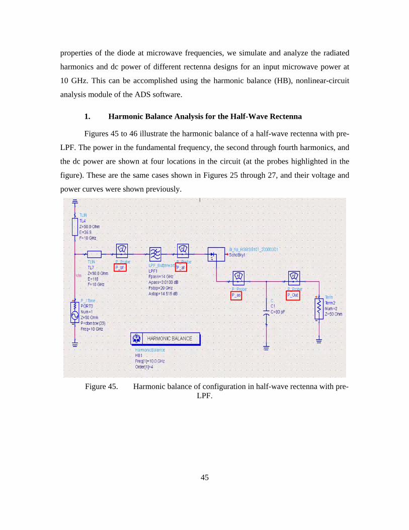
1. Harmonic Balance Analysis for the Half-Wave Rectenna
Figures 45 to 46 illustrate the harmonic balance of a half-wave rectenna with pre-
LPF. The power in the fundamental frequency, the second through fourth harmonics, and
the dc power are shown at four locations in the circuit (at the probes highlighted in the
figure). These are the same cases shown in Figures 25 through 27, and their voltage and
power curves were shown previously.
Figure 45. Harmonic balance of configuration in half-wave rectenna with pre-LPF.
46
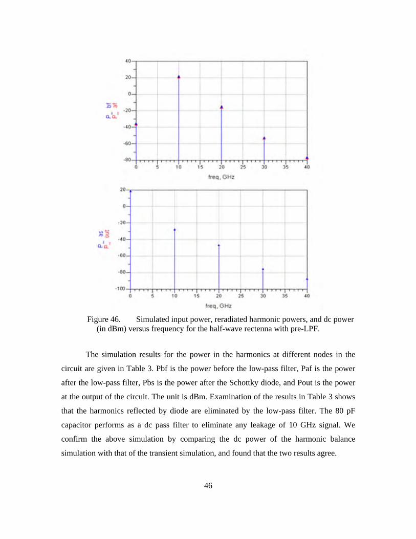
Figure 46. Simulated input power, reradiated harmonic powers, and dc power (in dBm) versus frequency for the half-wave rectenna with pre-LPF.
The simulation results for the power in the harmonics at different nodes in the
circuit are given in Table 3. Pbf is the power before the low-pass filter, Paf is the power
after the low-pass filter, Pbs is the power after the Schottky diode, and Pout is the power
at the output of the circuit. The unit is dBm. Examination of the results in Table 3 shows
that the harmonics reflected by diode are eliminated by the low-pass filter. The 80 pF
capacitor performs as a dc pass filter to eliminate any leakage of 10 GHz signal. We
confirm the above simulation by comparing the dc power of the harmonic balance
simulation with that of the transient simulation, and found that the two results agree.
47
Harmonic balance analysis data for fundamental frequency of 10 GHz (Pin=23 dBm)
Node 0 Hz 10 GHz 20 GHz 30 GHz 40 GHz
Pbf (dBm) -34.302 22.887 -13.708 -51.469 -75.358
Paf (dBm) -34.302 22.887 -13.708 -51.469 -75.358
Pas (dBm) 19.634 -26.804 -45.813 -74.595 -86.818
Pout (dBm) 19.634 -26.804 -45.813 -74.595 -86.818
Table 3. Harmonic balance data for the half-wave rectenna with pre-LPF.
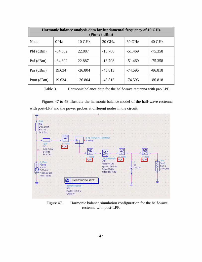
Figures 47 to 48 illustrate the harmonic balance model of the half-wave rectenna
with post-LPF and the power probes at different nodes in the circuit.
Figure 47. Harmonic balance simulation configuration for the half-wave rectenna with post-LPF.
48
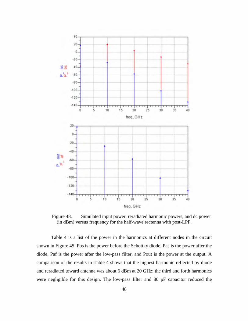
Figure 48. Simulated input power, reradiated harmonic powers, and dc power (in dBm) versus frequency for the half-wave rectenna with post-LPF.
Table 4 is a list of the power in the harmonics at different nodes in the circuit
shown in Figure 45. Pbs is the power before the Schottky diode, Pas is the power after the
diode, Paf is the power after the low-pass filter, and Pout is the power at the output. A
comparison of the results in Table 4 shows that the highest harmonic reflected by diode
and reradiated toward antenna was about 6 dBm at 20 GHz; the third and forth harmonics
were negligible for this design. The low-pass filter and 80 pF capacitor reduced the
49
harmonics produced by diode and produced stable dc power. We confirmed the above
simulation by comparing the dc power of harmonic balance simulation with the transient
simulation, and the results agree.
Harmonic balance analysis data for fundamental frequency of 10 GHz (Pin=23 dBm)
Node 0 Hz 10 GHz 20 GHz 30 GHz 40 GHz
Pbs (dBm) -34.555 22.342 5.914 -10.423 -28.589
Pas (dBm) 19.381 -25.154 -55.312 -99.631 -129.019
Paf (dBm) 19.381 -25.154 -55.312 -99.631 -129.019
Pout (dBm) 19.381 -25.154 -55.312 -99.631 -129.019
Table 4. Harmonic balance data for the half-wave rectenna with post-LPF.
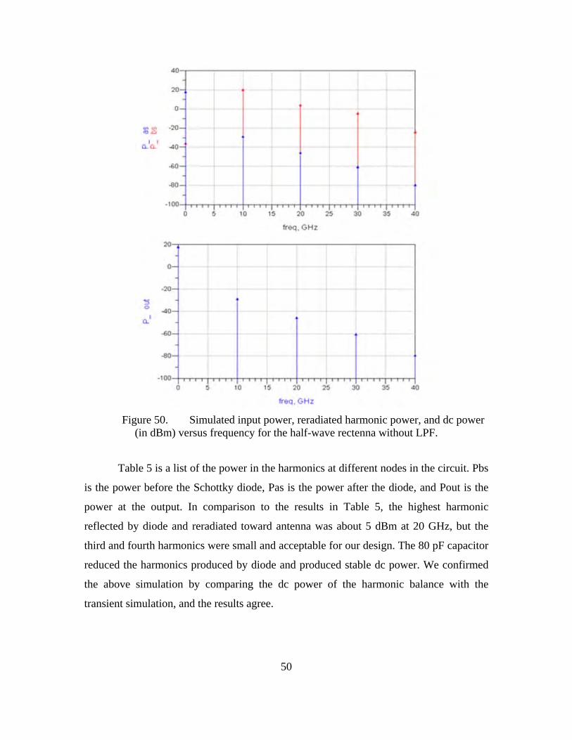
Figures 49 to 50 illustrate the harmonic balance of the half-wave rectenna without
LPF and the power in the fundamental frequency, harmonics, and dc at different nodes in
the circuit.
Figure 49. Harmonic balance simulation configuration for the half-wave rectenna without LPF.
50
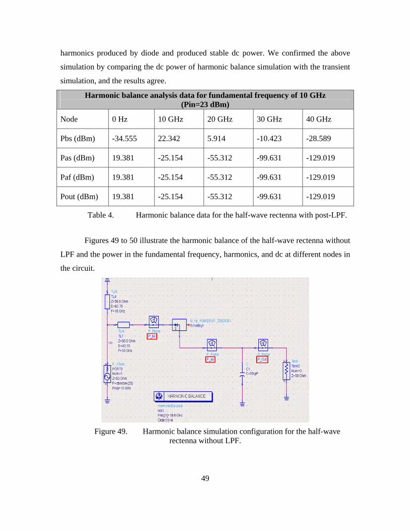
Figure 50. Simulated input power, reradiated harmonic power, and dc power (in dBm) versus frequency for the half-wave rectenna without LPF.
Table 5 is a list of the power in the harmonics at different nodes in the circuit. Pbs
is the power before the Schottky diode, Pas is the power after the diode, and Pout is the
power at the output. In comparison to the results in Table 5, the highest harmonic
reflected by diode and reradiated toward antenna was about 5 dBm at 20 GHz, but the
third and fourth harmonics were small and acceptable for our design. The 80 pF capacitor
reduced the harmonics produced by diode and produced stable dc power. We confirmed
the above simulation by comparing the dc power of the harmonic balance with the
transient simulation, and the results agree.
51
Harmonic balance analysis data for fundamental frequency of 10 GHz (Pin=23 dBm)
Node 0 Hz 10 GHz 20 GHz 30 GHz 40 GHz
Pbs (dBm) -35.061 21.128 4.968 -3.422 -22.986
Pas (dBm) 18.876 -27.815 -44.730 -59.540 -78.615
Pout (dBm) 18.876 -27.815 -44.730 -59.540 -78.615
Table 5. Harmonic-balance data for the half-wave rectenna without LPF.
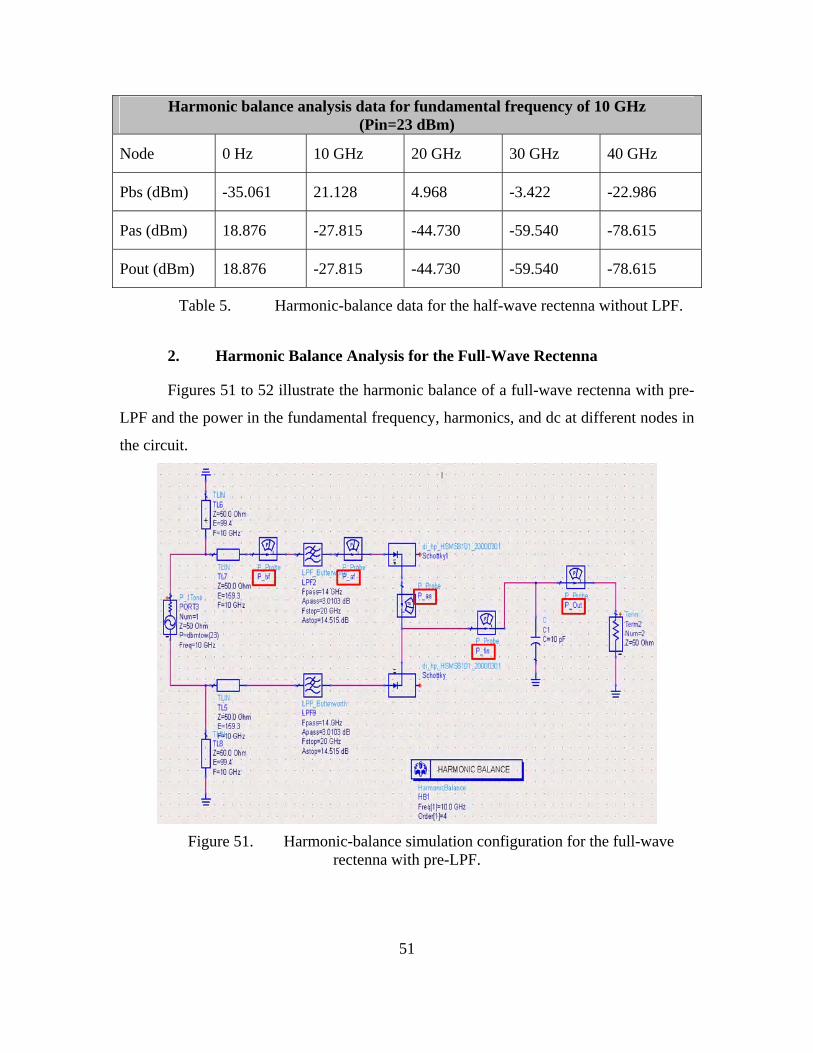
2. Harmonic Balance Analysis for the Full-Wave Rectenna
Figures 51 to 52 illustrate the harmonic balance of a full-wave rectenna with pre-
LPF and the power in the fundamental frequency, harmonics, and dc at different nodes in
the circuit.
Figure 51. Harmonic-balance simulation configuration for the full-wave rectenna with pre-LPF.
52
Figure 52. Simulated input power, reradiated harmonic power, and dc power (in dBm) versus frequency in full-wave rectenna with pre-LPF.
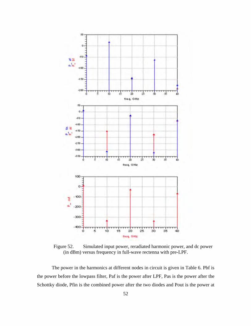
The power in the harmonics at different nodes in circuit is given in Table 6. Pbf is
the power before the lowpass filter, Paf is the power after LPF, Pas is the power after the
Schottky diode, Pfin is the combined power after the two diodes and Pout is the power at

53
the output of the circuit. The harmonics reflected by diode were eliminated by the low-
pass filter. The full-wave architecture essentially eliminates the frequencies of 10 GHz
and 30 GHz at the output. The 10 pF capacitor performs as a dc pass filter to eliminate
the frequencies 20 GHz and 40 GHz. These simulation results were compared to the
transient simulation, and the results agree.
Harmonic balance analysis data for fundamental frequency of 10 GHz (Pin=23 dBm)
Node 0 Hz 10 GHz 20 GHz 30 GHz 40 GHz
Pbf (dBm) -40.149 19.934 -145.177 -59.528 -188.391
Paf (dBm) -40.149 19.934 -140.204 -59.528 -172.270
Pas (dBm) 16.797 -145.791 -23.490 -170.867 -63.062
Pfin (dBm) 19.808 -304.622 -20.480 -313.664 -60.051
Pout (dBm) 19.808 -326.624 -20.480 -330.596 -60.051
Table 6. Harmonic balance data for the full-wave rectenna with pre-LPF.
Figures 53 to 54 illustrate the harmonic balance of the full-wave rectenna with
post-LPF and the power in the fundamental, harmonics, and dc at different nodes in
circuit.

54
Figure 53. Harmonic-balance simulation configuration for the full-wave rectenna with post-LPF.
55
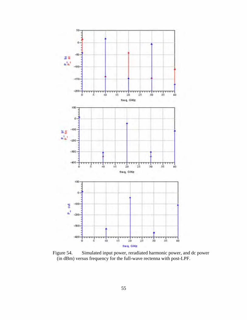
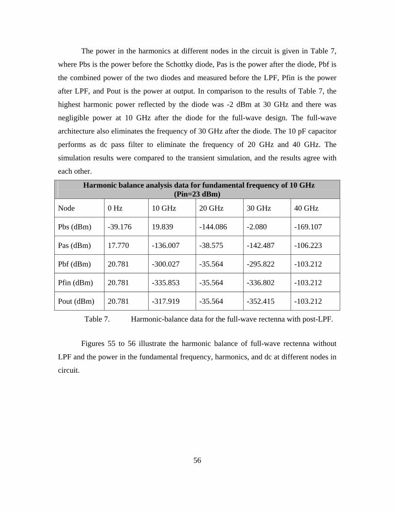
Figure 54. Simulated input power, reradiated harmonic power, and dc power (in dBm) versus frequency for the full-wave rectenna with post-LPF.
56
The power in the harmonics at different nodes in the circuit is given in Table 7,
where Pbs is the power before the Schottky diode, Pas is the power after the diode, Pbf is
the combined power of the two diodes and measured before the LPF, Pfin is the power
after LPF, and Pout is the power at output. In comparison to the results of Table 7, the
highest harmonic power reflected by the diode was -2 dBm at 30 GHz and there was
negligible power at 10 GHz after the diode for the full-wave design. The full-wave
architecture also eliminates the frequency of 30 GHz after the diode. The 10 pF capacitor
performs as dc pass filter to eliminate the frequency of 20 GHz and 40 GHz. The
simulation results were compared to the transient simulation, and the results agree with
each other.
Harmonic balance analysis data for fundamental frequency of 10 GHz (Pin=23 dBm)
Node 0 Hz 10 GHz 20 GHz 30 GHz 40 GHz
Pbs (dBm) -39.176 19.839 -144.086 -2.080 -169.107
Pas (dBm) 17.770 -136.007 -38.575 -142.487 -106.223
Pbf (dBm) 20.781 -300.027 -35.564 -295.822 -103.212
Pfin (dBm) 20.781 -335.853 -35.564 -336.802 -103.212
Pout (dBm) 20.781 -317.919 -35.564 -352.415 -103.212
Table 7. Harmonic-balance data for the full-wave rectenna with post-LPF.
Figures 55 to 56 illustrate the harmonic balance of full-wave rectenna without
LPF and the power in the fundamental frequency, harmonics, and dc at different nodes in
circuit.
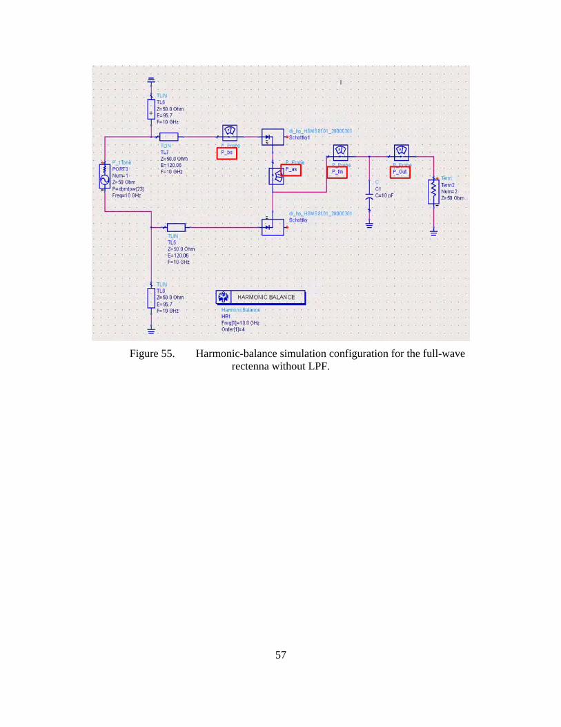
57
Figure 55. Harmonic-balance simulation configuration for the full-wave rectenna without LPF.

58
Figure 56. Simulated input power, reradiated harmonic power, and dc power (in dBm) versus frequency for the full-wave rectenna without LPF.
The simulation results for the power in the harmonics at different nodes in the
circuit are given in Table 8. Pbs is the power before the Schottky diode, Pas is the power
after the diode, Pfin is the combined power of the two diodes before the capacitor, and
Pout is the power at the output. In comparison to the results in Table 8, the highest
harmonic power generated by the diode was -3 dBm at 30 GHz and there was negligible
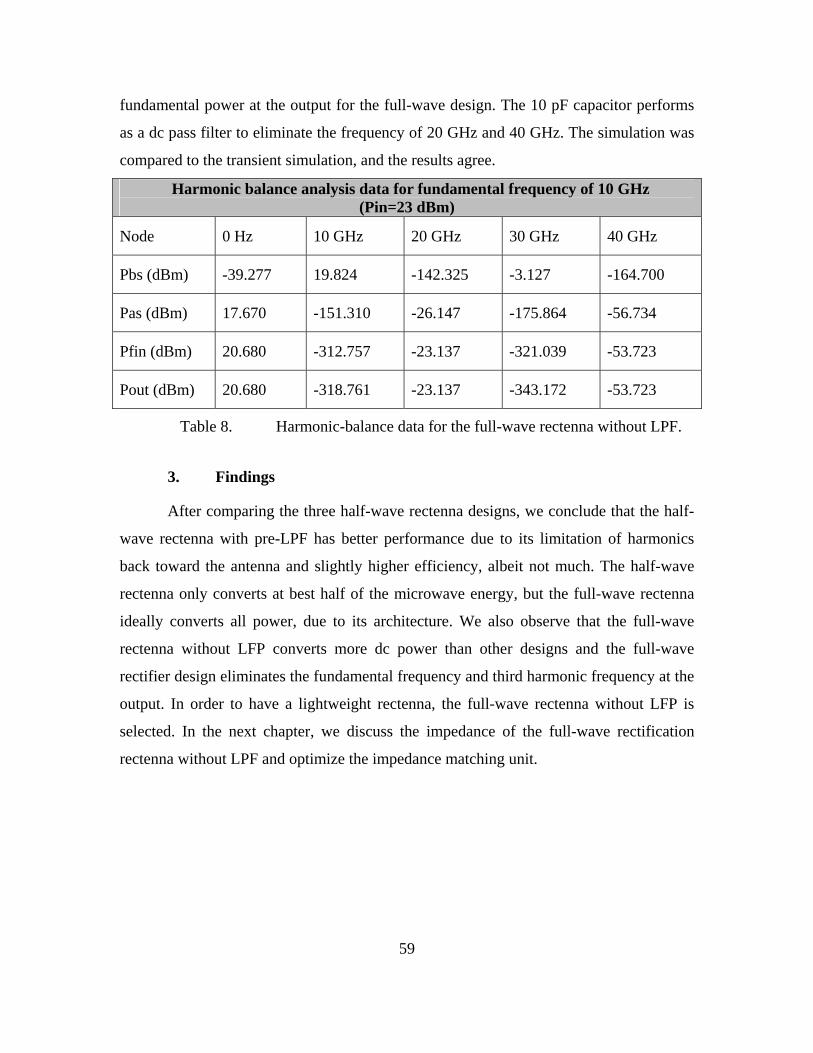
59
fundamental power at the output for the full-wave design. The 10 pF capacitor performs
as a dc pass filter to eliminate the frequency of 20 GHz and 40 GHz. The simulation was
compared to the transient simulation, and the results agree.
Harmonic balance analysis data for fundamental frequency of 10 GHz (Pin=23 dBm)
Node 0 Hz 10 GHz 20 GHz 30 GHz 40 GHz
Pbs (dBm) -39.277 19.824 -142.325 -3.127 -164.700
Pas (dBm) 17.670 -151.310 -26.147 -175.864 -56.734
Pfin (dBm) 20.680 -312.757 -23.137 -321.039 -53.723
Pout (dBm) 20.680 -318.761 -23.137 -343.172 -53.723
Table 8. Harmonic-balance data for the full-wave rectenna without LPF.
3. Findings
After comparing the three half-wave rectenna designs, we conclude that the half-
wave rectenna with pre-LPF has better performance due to its limitation of harmonics
back toward the antenna and slightly higher efficiency, albeit not much. The half-wave
rectenna only converts at best half of the microwave energy, but the full-wave rectenna
ideally converts all power, due to its architecture. We also observe that the full-wave
rectenna without LFP converts more dc power than other designs and the full-wave
rectifier design eliminates the fundamental frequency and third harmonic frequency at the
output. In order to have a lightweight rectenna, the full-wave rectenna without LFP is
selected. In the next chapter, we discuss the impedance of the full-wave rectification
rectenna without LPF and optimize the impedance matching unit.

60
THIS PAGE INTENTIONALLY LEFT BLANK
Equation Chapter 4 Section 1Equation Chapter 4 Section 1
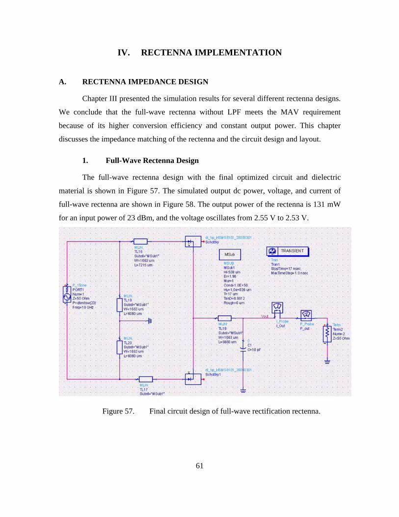
61
IV. RECTENNA IMPLEMENTATION
A. RECTENNA IMPEDANCE DESIGN
Chapter III presented the simulation results for several different rectenna designs.
We conclude that the full-wave rectenna without LPF meets the MAV requirement
because of its higher conversion efficiency and constant output power. This chapter
discusses the impedance matching of the rectenna and the circuit design and layout.
1. Full-Wave Rectenna Design
The full-wave rectenna design with the final optimized circuit and dielectric
material is shown in Figure 57. The simulated output dc power, voltage, and current of
full-wave rectenna are shown in Figure 58. The output power of the rectenna is 131 mW
for an input power of 23 dBm, and the voltage oscillates from 2.55 V to 2.53 V.
Figure 57. Final circuit design of full-wave rectification rectenna.
62
Figure 58. Simulated output power, voltage, and current-versus-time for the full-wave rectenna with a 23 dBm input.
2. Performance of Full-Wave Rectenna Impedance Design
The simulated conversion efficiency of the full-wave rectenna as a function of
input power is shown in Figure 59. The full-wave design is able to convert microwave
power to dc power with an efficiency of 65.9% at an input power of 200 mW. The
simulated output power of the full-wave rectenna design is shown in Figure 60. The full-
wave design is able to produce 132 mW at an input power of 200 mW. In addition, the
full-wave input–output characteristic is nearly linear, from 20 mW to 200 mW. From 200
mW to 400 mW of input power, the output begins to saturate. As a result, we prefer using
the full-wave rectenna design for MAV application at an input power of 200 mW because
it achieves the highest efficiency. However, to obtain this high power output requires a
very large power density at the antenna, as observed in Figure 19.
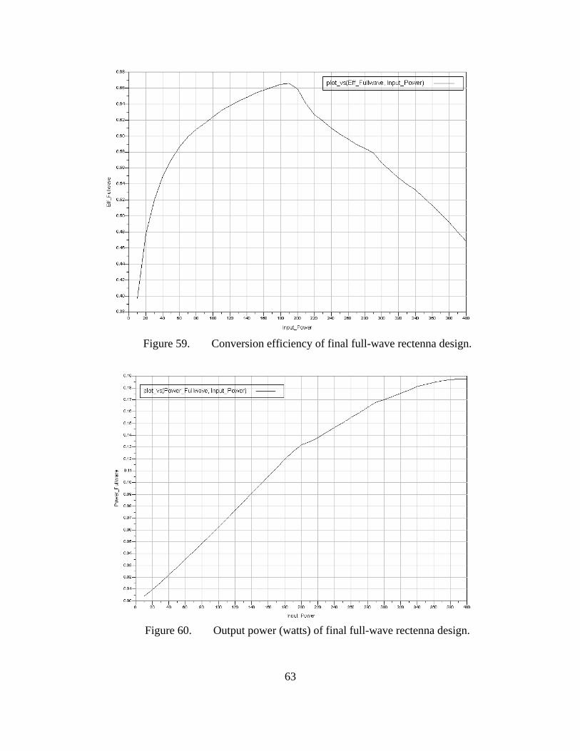
63
Figure 59. Conversion efficiency of final full-wave rectenna design.
Figure 60. Output power (watts) of final full-wave rectenna design.
64
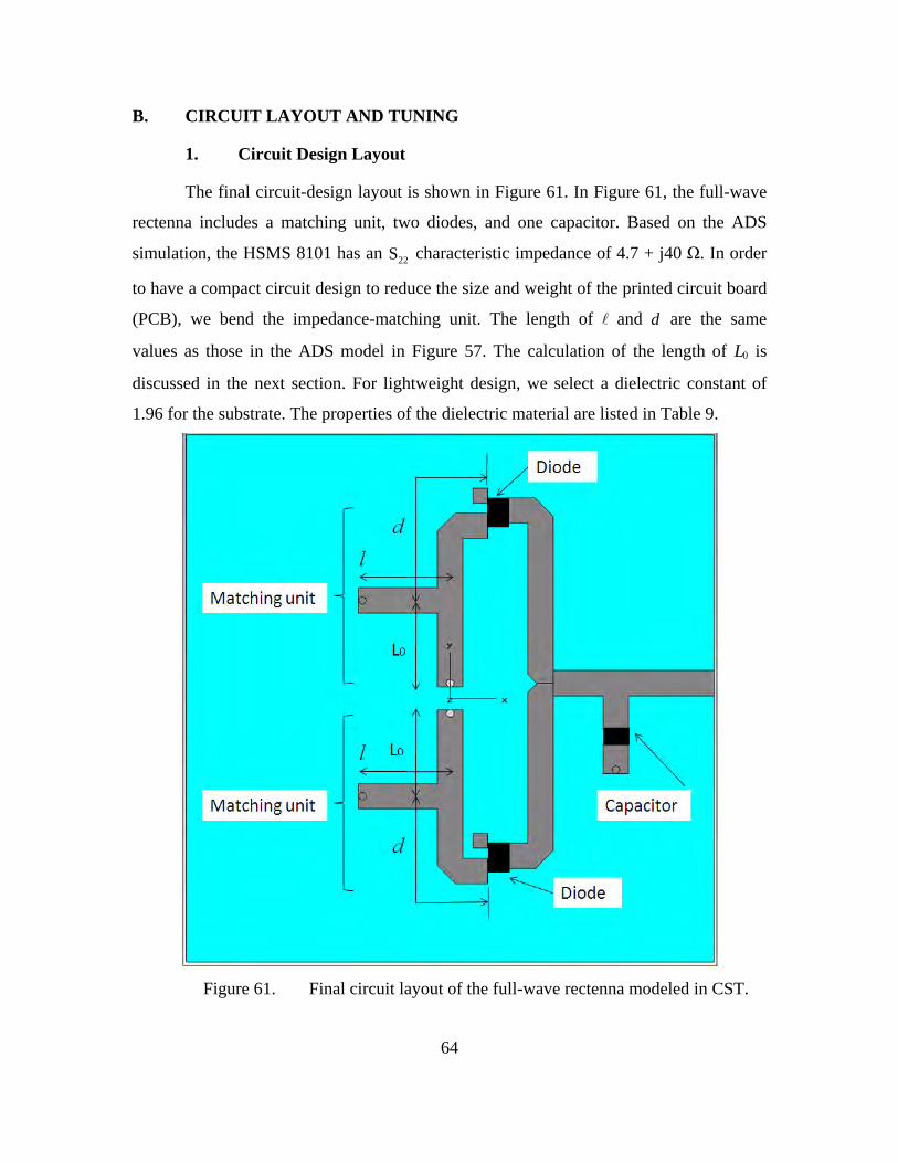
B. CIRCUIT LAYOUT AND TUNING
1. Circuit Design Layout
The final circuit-design layout is shown in Figure 61. In Figure 61, the full-wave
rectenna includes a matching unit, two diodes, and one capacitor. Based on the ADS
simulation, the HSMS 8101 has an 22S characteristic impedance of 4.7 + j40 Ω. In order
to have a compact circuit design to reduce the size and weight of the printed circuit board
(PCB), we bend the impedance-matching unit. The length of and d are the same
values as those in the ADS model in Figure 57. The calculation of the length of 0L is
discussed in the next section. For lightweight design, we select a dielectric constant of
1.96 for the substrate. The properties of the dielectric material are listed in Table 9.
Figure 61. Final circuit layout of the full-wave rectenna modeled in CST.

65
Dielectric Material Duroid 5880LZ from Rogers Corporation
Dielectric Constant r 1.96 0.04
Loss Tangent, tan 0.0019 @ 10 GHz
Substrate Height, h 0.508 mm microstrip circuit
Copper Thickness 0.5 oz or 17 μm
Table 9. Properties of Rogers Duroid 5880LZ.
2. Calculation of the Matching Unit
Figure 62 shows the portion of the circuit between an antenna terminal and the
diode. As seen in Figure 61, the circuit occurs at both dipole terminals. When a sinusoidal
voltage is applied at the terminals, one diode will conduct, appearing as a complex
impedance. The values of and d have been chosen to match the conducting diode to
the 50 Ω characteristic impedance of the line. This was done using the ADS parameter
sweep.
In order for the dipole to be matched at the conducting diode side, the other side
must present an open circuit at the antenna terminal. Therefore 0L must be chosen so that
the combination of the open circuit at the diode ( d ) and its matching stub ( ) present an
open circuit at the antenna terminal.

66
Figure 62. Circuit diagram showing the stub position.
The impedance of the shorted transmission line at the junction can expressed as
0
0 00
tantan
tanLs
insLs
Z jZZ Z jZ
Z jZ
(4.1)
and the admittance is
0
1 1
taninsins
YZ jZ
(4.2)
where 0Z is 50 Ω and LsZ is approximately 0 Ω. In addition, the impedance of the
transmission line d at the junction can be expressed as
0 00
0
tan
tan tanLd
indLd
Z jZ d ZZ Z
Z jZ d j d
(4.3)
where
4.7 40 conducting
nonconductingLd
jZ
(4.4)
and its admittance at the junction is
0
tan1.ind
ind
j dY
Z Z
(4.5)

67
The total admittance at the junction is
0 0
tan.
tantot ins ind
j djY Y Y
Z Z
(4.6)
The impedance looking into the junction must be transformed through a distance 0L .
0 0 00
0 0 0 0
tan 1 tan1
tan tantot tot
intot tot
Z jZ L jy LZ Z
Z jZ L y y j L
(4.7)
where 0
tottot
Yy
Y . Therefore
0
0
tan1.
1 tantot
inin tot
y j LY
Z jy L
(4.8)
The maximum power from the antenna occurs when inY equals to 0, therefore
0tan 0toty j L (4.9)
or
10
0
1tan .totY
L jY
(4.10)
This is the initial value of the length of the stub 0L which is a function of totY . The length
of this stub depends on the length of matching lines and d .
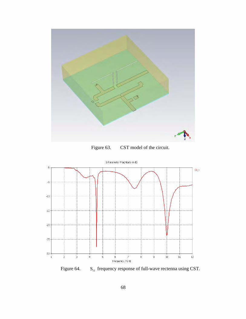
The parameter sweep in CST was used to fine-tune the value of 0L . Figure 63
shows the CST model of the circuit with one terminal of the dipole connected to a 50 Ω
line and the other diode open, to simulate a nonconducting half cycle. Figure 64 shows
the best match at 10 GHz obtained with the parameter sweep. The value of 0L is 4.226
mm, which was used in the final design. The radiation pattern for the circuit of Figure 63
is shown in Figure 65.
68
Figure 63. CST model of the circuit.
Figure 64. 11S frequency response of full-wave rectenna using CST.

69
Figure 65. Simulated result of the far-field radiation of full-wave rectenna using CST.

70
THIS PAGE INTENTIONALLY LEFT BLANK

71
V. SUMMARY, CONCLUSIONS AND RECOMMENDATIONS
A. SUMMARY
This thesis evaluated different rectenna designs for wireless power transmission
for MAV applications using the ADS simulation software. The first and second chapters
covered the history of WPT and research performed previously at NPS. Various
rectification circuit designs and antennas were simulated using Agilent ADS software and
CST Microwave Studio. A shorted stub microstrip tuner was introduced for impedance
matching. The dipole-antenna array was selected to reduce the weight of the rectenna in
order to hover a MAV.
A full-wave rectenna without low-pass filter was selected to reduce the weight of
the rectenna element yet achieve high conversion efficiency. In addition, a harmonic
balance analysis was conducted in order to compare the influence of the harmonics on
various circuit designs. The full-wave rectenna circuit was simulated to verify
performance, and the conversion efficiency is about 65%. The length of matching units
were calculated and optimized in Microwave Studio in order to lay out the circuit.
B. RECOMMENDATIONS
The result of this thesis shows that the improved full-wave rectanna converts
more dc power than a half-wave rectenna, as verified by simulation. A dipole antenna
was used instead of a circular-patch antenna in order to reduce the weight of the rectenna
system. The conversion efficiency of the rectenna can be improved, however, and some
recommendations follow.
1. Using High-Power Transmitter and High-Gain Antenna
The performance of the WPT can be further enhanced by complementing it with a
high-power transmitter and high-gain antenna to increase the power-density incident on
the rectenna array.

72
2. Building a Hardware Prototype
Upon the successful design of the dipole antenna and rectifier circuit using CST
Microwave Studio, it is necessary to build a prototype of the full-wave rectenna to
measure the output dc voltage and current and determine the realized efficiency.
3. Running Simulations for an Array
The MWS simulation should be done for an array of dipoles to assess the effect of
mutual coupling. The array element may need to be returned to compensate for the
mutual coupling.
4. Reducing Polarization Loss
The dipole is linearly polarized, and therefore loss of signal will occur if the
MAV antenna is orientated in a cross-polarized direction in flight. A circularly polarized
antenna should be considered to reduce the polarization loss factor.

73
LIST OF REFERENCES
[1] W. C. Brown, “The History of Power Transmission by Radio Waves,” IEEE Transactions on Microwave Theory and Techniques, Vol. MTT-32, No. 9, September 1984.
[2] J. J. Schlesak, Adrian Alden and Tom Ohno, “A Microwave Powered High Altitude Platform,” IEEE MTT-S Digest, 1988.
[3] M. Mecham, “California’s PG&E links with startup on 200-megawatt SSP initiative,” Aviation Week & Space Technology, April 2009.
[4] S. V. Georgakopoulos and S. Jiang, “Wireless Powering of Sensors Embedded in Concrete,” Wireless and Microwave Technology IEEE 11th Annual Conference, 2010.
[5] U. Olgun, C.-C.Chen and J. L. Volakis, “Investigation of Rectenna Array Configurations for Enhanced RF Power Harvesting,” IEEE Antennas and Wireless Propagation Letters, vol. 10, no. 1, pp. 262–265, April 2011.
[6] M. T. L. Meng, “Efficient Rectenna Design for Wireless Power Transmission For MAV application,” Naval Postgraduate School, December 2005.
[7] L. H. Toh, “A Follow-up Study on Wireless Power Transmission for Unmanned Air Vehicles,” Naval Postgraduate School, December 2007.
[8] G. Tsolis, “Theoretical and experimental study of micro air vehicle powered by RF Signal at 10 GHz,” Naval Postgraduate School, December 2003.
[9] W. C. Brown, “Description and operating characteristics of the platinotron – A new microwave tub device,” Proc. IRE, vol. 45, no. 9, pp.1209–1222, September 1957.
[10] G. Goubau and F. Schwering, “On the guided propagation of electromagnetic wave beams,” IRE Transactions on Antenna Propagation, vol. AP-9, pp.248–256, May 1961.
[11] D.-G.Youn, Y.-H. Park, K.-H. Kim and Y.-C. Rhee, “A Study on the Fundamental Transmission Experiment for Wireless Power Transmission System,” 1999 IEEE TENCON.
[12] J. A. Hagerty, F. B. Helmbrecht, W. H. McCalpin, R. Zane and Z. B. Popovic, “Recycling Ambient Microwave Energy With Broad-Band Rectenna Arrays,” IEEE Transactions on Microwave Theory and Techniques, vol. 52, no. 3, pp.1014–1024, March 2004.

74
[13] J. O. McSpadden and J. C. Mankins, “Space Solar Power Programs and Microwave Wireless Power Transmission Technology” IEEE Microwave Magazine, December 2002.
[14] A.goel, R.P. Jamdagni, and N. K. Mishra, “New Hope for Clean Energy through Exploring Space,” Recent Advances in Space Technology Services and Climate Change, pp 87–89, November 2010.
[15] Y.-H. Suh and K. Chang, “A High-Efficiency Dual-Frequency Rectenna for 2.45- and 5.8-GHz Wireless Power Transmission,” IEEE Transactions on Microwave Theory and Techniques, vol. 50, no. 7, pp.1784–1789, July 2002.
[16] B. Strassner, S. Kokel and K. Chang, “5.8 GHz Circularly Polarized Low Incident Power Density Rectenna Design and Array Implementation,” IEEE Antennas and Propagation Society International Symposium, vol. 3, pp.950–953, June 2003.
[17] J.-Y. Park, S.-M. Han and T. Itoh, “A Rectenna Design With Harmonic-Rejecting Circular-Sector Antenna,” IEEE Antennas and Wireless Propagation Letters, vol. 3, no. 1, pp.52–54, December 2004.
[18] J. Zbitou, M. Latrach and S. Toutain, “Hybrid Rectenna and Monolithic Integrated Zero-Bias Microwave Rectifier,” IEEE Transaction on Microwave Theory and Techniques, vol. 54, no. 1, pp.147–152, January 2006.
[19] T. Yamamoto, K. Fujimori, M. Sanagi and S. Nogi, “The Design of mw-Class RF-DC Conversion Circuit using the Full-Wave Rectification,” The 37th European Microwave Conference, Proceeding, 9–12 October 2007, pp.905–908.
[20] U. Olgun, C.-C. Chen and J. L. Volakis, “Low-profile Planar Rectenna for Batteryless RFID Sensors,” IEEE Antennas and Propagation Society International Symposium, pp.1–4, July 2010.
[21] R. L. Vitale, “Design and Prototype Development of a Wireless Power Transmission System For a Micro Air Vehicle (MAV),” Naval Postgraduate School, June 1999.
[22] T.-W. Yoo and K. Chang, “Theoretical and Experimental Development of 10 and 35 GHz Rectennas,” IEEE Transactions on Microwave Theory and Techniques, vol. 40, no. 6, pp.1259–1266, June 1992.
[23] H.-K. Chiou and I.-S. Chen, “High-Efficiency Dual-Band On-chip Rectenna for 35- and 94-GHz Wireless Power Transmission in 0.13-μm CMOS Technology,” IEEE Transactions on Microwave Theory and Techniques, vol. 58, no. 12, pp. 3598–3606, December 2010.
[24] F. T. Ulaby, Fundamentals of Applied Electromagnetics, pp.88–92, Prentice Hall, Person Education Inc, 2004.

75
INITIAL DISTRIBUTION LIST
1. Defense Technical Information Center Ft. Belvoir, Virginia 2. Dudley Know Library Naval Postgraduate School Monterey, California 3. Dan C. Boger Chairman, Information Science Department Naval Postgraduate School Monterey, California 4. Professor David C. Jenn Professor, Department of Electrical & Computer Engineering Naval Postgraduate School Monterey, California 5. Professor Ric Romero Assistant Professor, Department of Electrical & Computer Engineering Naval Postgraduate School Monterey, California 6. Robert D. Broadston Staff, Department of Electrical & Computer Engineering Naval Postgraduate School Monterey, California 7. Chun-Yi Liu Department of Electronic Warfare Systems Engineering Naval Postgraduate School Monterey, California 8. Deanna Y. Tyler US Army CERDEC, C2D Aberdeen, Maryland