Embed Size (px)
Citation preview

Long-Term Reliability of High Speed SiGe/Si Heterojunction Bipolar Transistors
NASA-GRC Grant No. NAG3-2530
NASA Technical Officer Dr. George E. Ponchak
Electron Device Technology Branch Mail Stop 54-5
NASA-Glenn Research Center 2 1000 Brookpark Road
Cleveland, Ohio 44 135-3 19 1
Principal Investigator Professor Pallab Bhattacharya
Department of Electrical Engineering and Computer Science University of Michigan
Ann Arbor, MI 48 109-2 122 Phone: (734) 763-6678
Email: pkb @eecs.umich.edu FAX: (734) 763-9324
https://ntrs.nasa.gov/search.jsp?R=20030061418 2018-05-23T09:06:36+00:00Z
.
Long-Term Reliability of High Speed SiGdSi Heterojunction Bipolar Transistors
Principal Investigator Professor Pallab Bhattacharya
Department of Electrical Engineering and Computer Science University of Michigan
Ann Arbor, MI 48109-2122
Abstract
Accelerated lifetime tests were performed on double-mesa structure Si/Si,,,Ge,,/Si npn heterojunction bipolar transistors, grown by molecular beam epitaxy, in the temperature range of 175"C-275"C. Both single- and multiple finger transistors were tested. The single-finger transistors (with 5x20 pm2 emitter area) have DC current gains - 40-50 and fT and f,, of up to 22 GHz and 25 GHz, respectively. The multiple finger transistors (1.4 pm finger width, 9 emitter fingers with total emitter area of 403 pm') have similar DC current gain but fT of 50 GHz. It is found that a gradual degradation in these devices is caused by the recombination enhanced impurity diffusion (REID) of boron atoms from the p-type base region and the associated formation of parasitic energy barriers to electron transport from the emitter to collector layers. Th i s REID has been quantitatively modeled and explained, to the first order of approximation, and the agreement with the measured data is good. The mean time to failure (MTTF) of the devices at room temperature is estimated from the extrapolation of the Arrhenius plots of device lifetime versus reciprocal temperature. The results of the reliability tests offer valuable feedback for SiGe heterostructure design in order to improve the long-term reliability of the devices and circuits made with them. Hot electron induced degradation of the base-emitter junction was also observed during the accelerated lifetime testing. In order to improve the HBT reliability endangered by the hot electrons, deuterium sintered techniques have been proposed. The preliminary results from this study show t h a t a deuterium-sintered HBT is, indeed, more resistant to hot-electron induced base-emitter
2
junction degradation. SiGe/Si based amplifier circuits were also subjected to lifetime testing and we extrapolate MTTF - 1.1-106 hours at 125iC junction temperature from the circuit lifetime data.
3
1. INTRODUCTION
The rapid progress of Si/SiGe heterojunction bipolar transistor (HBT) technology has made Si-based devices very attractive for microwave applications. Among t h e existing SiGe technologies, Si/SiGe/Si HBTs have been most widely studied [1]- [SI owing to the advantage in material characteristics, such as the near-zero conduction band offset between Si and strained SiGe layers, which is preferred for npn HBT applications. The use of a smaller bandgap SiGe alloy in the base of the HBT increases the efficiency of minority carrier injection. This results in an increase of collector current and current gain even though the base doping is high. The high base doping yields a smaller base resistance, which in turn leads to high maximum oscillation frequency f-, high Early voltage and low noise figure. However, the p-n junctions in a HBT must be well defined and coincident with the heterojunctions. Base dopant outdiffusion during epitaxy and/or during device processing and operation shifts the location of p-n junctions, usually resulting in the formation of parasitic energy barriers near the base-emitter and base- collector junctions, which can significantly reduce the current gain and cutoff frequency
Device performance is a function of time in general, since the device performance parameters are liable to change, gradually or abruptly, as the operation time accumulates. Therefore, excellent performance observed during the initial measurement on a device does not necessarily guarantee long-term reliability. For the Si/SiGe HBT technology to be a choice for commercial radio frequency integrated circuits the long-term reliability of Si/SiGe HBTs has to be proven and, to our knowledge, very limited report on this subj ect exists in the literature. Neugroschel et aZ[8] have investigated the time-to-failure of GeSi bipolar transistors with current-acceleration method in which base-emitter reverse-bias stress was applied at room temperature. While this method can significantly accelerate the degradation of devices and is effective for observing the device degradation caused by hot carriers, it is not suitable for evaluating the device degradation caused by atomic diffusion. Another investigation, on the effects of base-emitter reverse-bias stress on the cryogenic operation of SiGe HBTs, has been reported by Babcock et aZ[9]. Specially tailored techniques are required to evaluate the long-term reliability of devices since it takes impractically long times to observe any appreciable degradation in the device performance under normal operating conditions. The long-term reliability can be m o s t effectively evaluated by accelerated lifetime testing (ALT), i.e., measuring the dev ice lifetime at elevated temperatures under normal bias conditions [lo]-[ 121. Unlike t h e current-acceleration method used by Neugroschel et aZ [8], this ALT method resembles the real operating condition of HBTs. By extrapolating the HBT lifetimes at h i g h temperatures from the Arrhenius plot, the mean time to failure (MTTF) of the device at room temperature can be estimated. The extrapolation is based on the assumption t h a t the degradation mechanism remains unchanged over the entire temperature range of testing and the same activation energy applies. The common sources of device degradation are diffusion of dopants, dielectric breakdown, surface or interface i o n migration, metal contact degradation, electromigration of metal lines, etc. In particular, boron outdiffusion is one of the major concerns in the context of thermal budget in t h e
[a 171.
4
fabrication and operation of SiGe/Si HBT, as it leads to the degradation of critical device parameters as mentioned above [7 ] . The accelerated lifetime test can be used as an effective tool to identify the source of degradation. Additionally, analysis of the failure mechanism can offer valuable feedback on the design of device structures for long-term reliability of the devices and circuits.
In this study, it has been found that forward-bias electrical-thermal stress can induce boron-outdi ffusion and associated degradation for double-mesa structure npn Si/SiGe HBTs. The degradation behavior has been quantitatively modeled, to the first order of approximation. The device failure mechanism has been analyzed and its impact on device heterostructure design for improvement of long-term reliability is discussed. In what follows, the experimental techniques are described in Section 2. The experimental results of the accelerated life-time testing will be presented and analyzed in Section 3. The REID model based on low-level injection theory is presented in Section 4. The comparison of hot-electron reliability between deuterium-sintered SiGe/Si HBT and the control HBT will be presented in Section 5 and the important results are summarized in Section 6 .
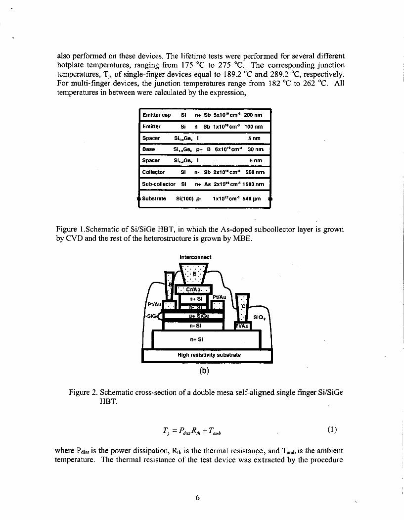
2. EXPERIMENTAL TECHNIQUES The HBTs used in this testing are grown by solid-source MBE. The devices (Fig. 1)
have a 30 nm boron doped Sio.7Geo.3 base layer with two undoped Si0.7Ge0.3 spacers of thickness 5 nm on each side of it. Antimony was used to dope the emitter and collector layers. The epitaxial heterostructures are fabricated into mesa type devices with 5x20 pm2 emitter size, using standard photolithography and wet and dry etching techniques. Multiple finger devices were also fabricated with 1 .4~20 pm2 finger size and 9 emitter fingers. The total emitter area, including emitter contact areas, is 403 pm2. Details of these procedures have been described in Ref.13. The schematic cross-section of a finished HBT (single finger cross section is drawn only) is shown in Fig. 2. T h e measurement setup used for the lifetime test is briefly described. The single finger device under test (DUT) was placed on a temperature-controlled hotplate and biased with collector-emitter voltage VCE and base current IB in the common-emitter configuration. VCE, supplied by a Keithley 230 voltage source, was fixed at 3 V, while IB, supplied by a Keithley 220 current source, was feedback-controlled by computer to maintain a constant collector current IC of 13.5 mA, which corresponds to a current density JC of 1.35 x10⁴ Ncm2 and dissipated DC power Pdiss of 40.5 mW. For the multiple finger devices, VCE of 3.5 V and JC of 1.75 x10⁴ A/cm2 were applied. It is necessary to maintain a constant collector current level, which can vary with a fixed base current due to the possible degradation of the current gain during the test, in order to keep a constant electrical stress condition throughout the entire duration of each test run. A HP2378A multimeter was included to monitor the collector current levels so that the base current could be adjusted by feedback-control in case of deviation from the acceptable range. The multimeter was also used to display the actual value of VCE applied to the devices. The test w a s performed without any interruption, the bias being applied to the devices continuously till they stopped operating. Post-stress measurements were then made. Identical devices on the same wafer, which were only subjected to thermal stress without any electrical stress during each test run, are classified as control devices and post-stress measurements were
5
also performed on these devices. The lifetime tests were performed for several different hotplate temperatures, ranging from 175 OC to 275 "C. The corresponding junction temperatures, Tj, of single-finger devices equal to 189.2 O C and 289.2 "C, respectively. For multi-finger devices, the junction temperatures range from 182 "C to 262 O C . All temperatures in between were calculated by the expression,
I Emitter cap Si n+ Sb 5x101*cmJ 200 nm I I Emitter Si n Sb lxlO'*cm" 100nm I I Spacer Si,,Ge. I 5nm I
~ _ _ _ _ _ ~~~ I Base Si,,G& p+ B 6 ~ 1 0 ' ~ c m ~ 30 n m l
I Spacer Si,,Ge. i ' 5nm I I Collector Si n- Sb 2 ~ 1 0 ~ ~ c m ~ 250nm I I Sub-collector Si n+ As 2 ~ 1 0 ' ~ c m ~ 1500 n m I + +Substrate Si(100) p- 1xlO'*cmJ 540 pn
Figure 1.Schematic of Si/SiGe HBT, in which the As-doped subcollector layer is grown by CVD and the rest of the heterostructure is grown by MBE.
Interconnect
I High resistivity substrate I
Figure 2. Schematic cross-section of a double mesa self-aligned single finger Si/SiGe HBT.
where Pdiss is the power dissipation, Rh is the thermal resistance, and Tamb is the ambient temperature. The thermal resistance of the test device was extracted by the procedure
6
outlined in Ref. 14. After VBE is measured as a function of DC power dissipation with increasing VCE and a fixed IC at room temperature, VBE is measured as a fimction of temperature with both VCE and IC fixed. The two plots are then combined and a relation between the temperature and the DC power dissipation is obtained. The slope of this plot corresponds to the thermal resistance Rth, which was 350 OC/W (170 OC/W for multiple fingers) in this case. It is assumed in this calculation that the hotplate temperature is close to the junction temperature of the device, which is the case for the soft bias used in the measurements.
The acceleration of base-emitter junction degradation was performed by applying a reverse bias (VBE= -3.5 V) on the base-emitter junction and a forward bias (VBc = 1.2 V) on the base-collector junction, as proposed by Neugroschel [8] so that a much larger hot electron stream can be applied across the base-emitter junction. This acceleration scheme is called current acceleration and it was performed at the room temperature. T h e degradation of the device was monitored with the measurement (under VBE = 0.65 V a n d VCE = 4V) of DC current gain, p, at a certain time interval. Two identical devices were tested with one subjected to deuterium sintering and the other without any sintering as the control device.
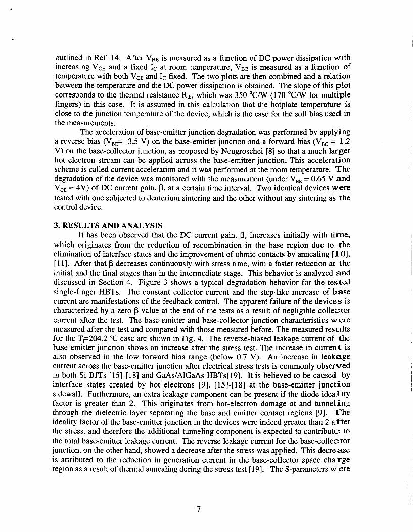
3. RESULTS AND ANALYSIS It has been observed that the DC current gain, p, increases initially with t ime,
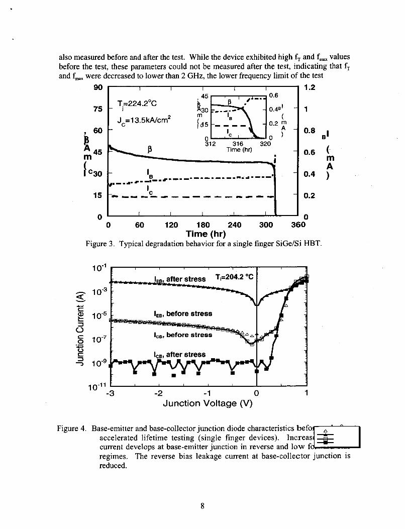
which originates from the reduction of recombination in the base region due to the elimination of interface states and the improvement of ohmic contacts by annealing [ 1 01, [ l 11. After that p decreases continuously with stress time, with a faster reduction at the initial and the final stages than in the intermediate stage. This behavior is analyzed a n d discussed in Section 4. Figure 3 shows a typical degradation behavior for the tested single-finger HBTs. The constant collector current and the step-like increase of base current are manifestations of the feedback control. The apparent failure of the devices is characterized by a zero p value at the end of the tests as a result of negligible collector current after the test. The base-emitter and base-collector junction characteristics were measured after the test and compared with those measured before. The measured results for the Tj=204.2 "C case are shown in Fig. 4. The reverse-biased leakage current of the base-emitter junction shows an increase after the stress test. The increase in current is also observed in the low forward bias range (below 0.7 V). An increase in leakage current across the base-emitter junction after electrical stress tests is commonly observed in both Si BJTs [15]-[18] and GaAs/AlGaAs HBTs[l9]. It is believed to be caused by interface states created by hot electrons [9], [ 151-[ 181 at the base-emitter junction sidewall. Furthermore, an extra leakage component can be present if the diode ideality factor is greater than 2. This originates from hot-electron damage at and tunneling through the dielectric layer separating the base and emitter contact regions [9]. T h e ideality factor of the base-emitter junction in the devices were indeed greater than 2 after the stress, and therefore the additional tunneling component is expected to contribute to the total base-emitter leakage current. The reverse leakage current for the base-collec tor junction, on the other hand, showed a decrease after the stress was applied. This decrease is attributed to the reduction in generation current in the base-collector space charge region as a result of thermal annealing during the stress test [19]. The S-parameters w e r e
7
.
also measured before and after the test. While the device exhibited high fT and f,, values before the test, these parameters could not be measured after the test, indicating that fT
and f- were decreased to lower than 2 GHz, the lower frequency limit of the test 90
75
b 6o A 45 m
1 c30
15
0
I I I I I 1 1.2
1
0.8 I B
0 60 120 180 240 300 360
Figure 3. Typical degradation behavior for a single finger SiGe/Si HBT. Time (hr)
1
1 0-1
10-3
10-5
1 o - ~
10-9
0-11 . I I I I I I
a
-3 -2 -1 0 1 Junction Voltage (V)
Figure 4. Base-emitter and base-collector junction diode characteristics befo accelerated lifetime testing (single finger devices). current develops at base-emitter junction in reverse regimes. The reverse bias leakage current at base-collector junction is reduced.
8
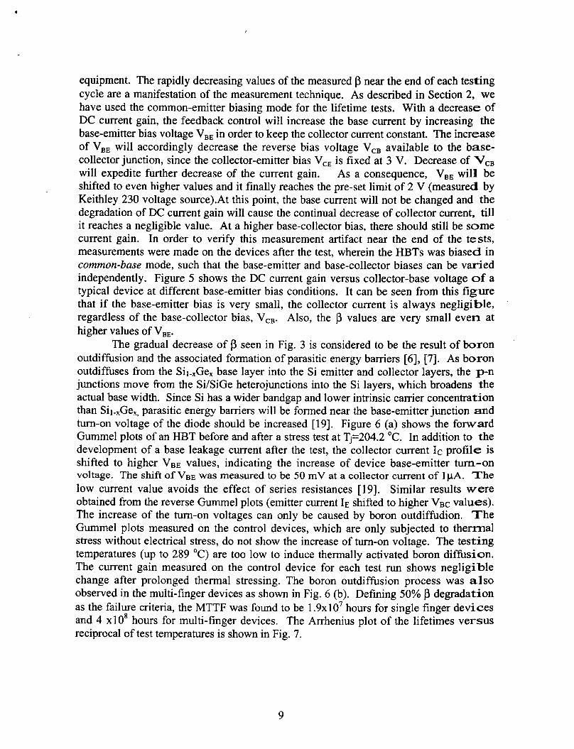
equipment. The rapidly decreasing values of the measured p near the end of each testing cycle are a manifestation of the measurement technique. As described in Section 2, we have used the common-emitter biasing mode for the lifetime tests. With a decrease of DC current gain, the feedback control will increase the base current by increasing the base-emitter bias voltage VBE in order to keep the collector current constant. The increase of VBE will accordingly decrease the reverse bias voltage V,, available to the base- collector junction, since the collector-emitter bias V,, is fixed at 3 V. Decrease of VcB will expedite further decrease of the current gain. As a consequence, VBE will be shifted to even higher values and it finally reaches the pre-set limit of 2 V (measured by Keithley 230 voltage source).At this point, the base current will not be changed and the degradation of DC current gain will cause the continual decrease of collector current, till it reaches a negligible value. At a higher base-collector bias, there should still be some current gain. In order to verify this measurement artifact near the end of the tests, measurements were made on the devices after the test, wherein the HBTs was biased in common-base mode, such that the base-emitter and base-collector biases can be varied independently. Figure 5 shows the DC current gain versus collector-base voltage of a typical device at different base-emitter bias conditions. It can be seen from this figure that if the base-emitter bias is very small, the collector current is always negligible, regardless of the base-collector bias, VcB. Also, the p values are very small even at higher values of VBE.
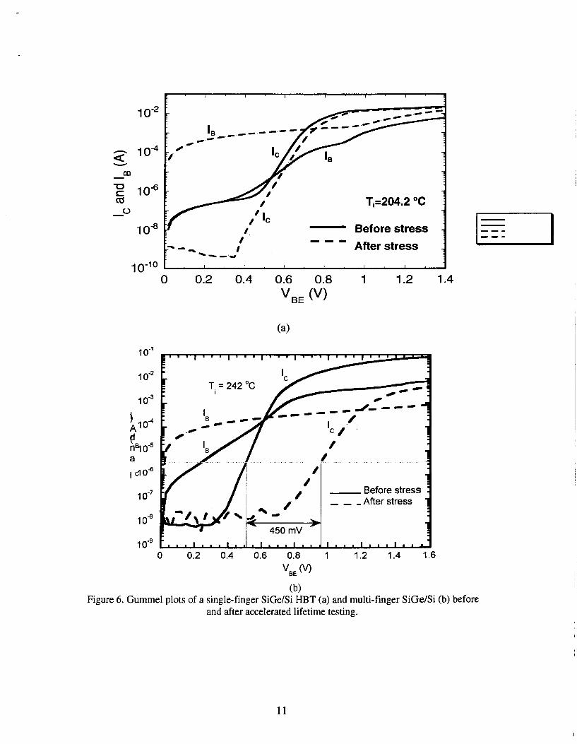
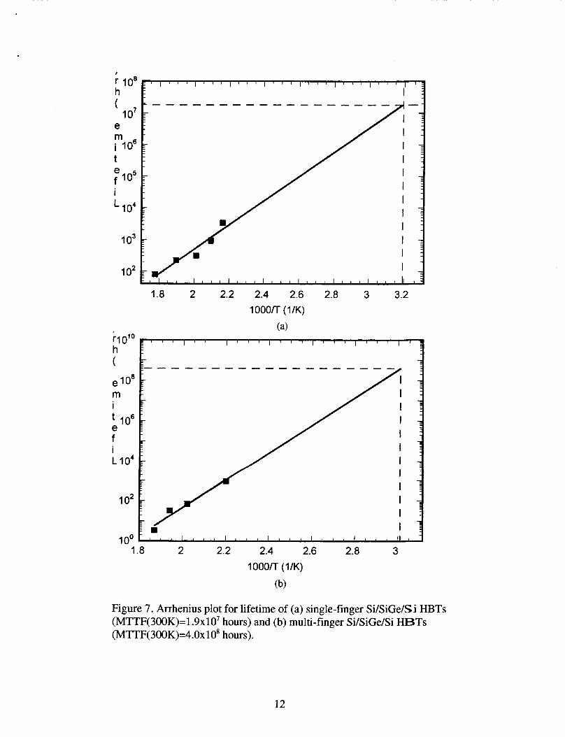
The gradual decrease of p seen in Fig. 3 is considered to be the result of boron outdiffusion and the associated formation of parasitic energy barriers [6], [7]. As boron outdiffuses from the Sil-,Ge, base layer into the Si emitter and collector layers, the p-n junctions move from the Si/SiGe heterojunctions into the Si layers, which broadens the actual base width. Since Si has a wider bandgap and lower intrinsic carrier concentration than Sil_,Ge, parasitic energy barriers will be formed near the base-emitter junction a n d turn-on voltage of the diode should be increased [19]. Figure 6 (a) shows the forward Gummel plots of an HBT before and after a stress test at Tjz204.2 "C. In addition to the development of a base leakage current after the test, the collector current IC profile is shifted to higher VBE values, indicating the increase of device base-emitter turn-on voltage. The shift of VBE was measured to be 50 mV at a collector current of 1pA. T h e low current value avoids the effect of series resistances [19]. Similar results w e r e obtained from the reverse Gummel plots (emitter current IE shifted to higher VBC values). The increase of the turn-on voltages can only be caused by boron outdiffudion. 'The Gummel plots measured on the control devices, which are only subjected to thermal stress without electrical stress, do not show the increase of turn-on voltage. The testing temperatures (up to 289 "C) are too low to induce thermally activated boron diffusion. The current gain measured on the control device for each test run shows negligible change after prolonged thermal stressing. The boron outdiffusion process was also observed in the multi-finger devices as shown in Fig. 6 (b). Defining 50% p degradation as the failure criteria, the MTTF was found to be 1 . 9 ~ 1 0 ~ hours for single finger devices and 4 x10⁸ hours for multi-finger devices. The Arrhenius plot of the lifetimes versus reciprocal of test temperatures is shown in Fig. 7.
9
4. DIFFUSION MODEL FOR GRADUAL DEGRADATION Since boron outdiffusion occurs during the testing, a further step was taken to
analyze the outdiffusion-related gradual degradation behavior with a simple diffusion model as outlined below. All the analysis is based on low-level injection theory, since the base-emitter bias during the gradual p degradation is about 0.6-0.7 V.
In a npn SiGe HBT, the collector current density J,, assuming absence of hot- electron effects, can be expressed as [23], [24]:
8
6
u 4
2
V,,=0.5 V 0
0 1 2 3 4 5 6 v,, (V)
Figure 5. DC current gain versus base-collector bias voltage at different base-emitter biases after accelerated lifetime testing (single-finger
+ - (2)
where W, is the neutral base width, V,, is the base-emitter voltage, p(x) is the base doping, D,(x) is the minority carrier diffusion coefficient and n,(x) is the intrinsic carrier concentration of SiGe base, respectively. Assuming that the base current is generated
only by hole injection from base into emitter, it is modeled as [20] J B = J B O ~ ~ and the analytical current gain takes the form:
4 'BE
10
h a v
m - U c ca
lo-*
1 o4
1 o4
1 os
E I I I I I I
-
Before stress - I I I 1 I I 1
0 0.2 0.4 0.6 0.8 1 1.2 1.4
lo- '
1 o-2
a , do6
1 o-'
10"
10" r . I I I I . I I I .I I I I I . I I I 1 I I I I I I I I I I I . 1 0 0.2 0.4 0.6 0.8 1 1.2 1.4 1.6
VBE (V)
I= I
(b) Figure 6. Gummel plots of a single-finger SiGe/Si HBT (a) and multi-finger SiGe/Si (b) before
and after accelerated lifetime testing.
11
IO8 h ( 10'
e
:I 06 t e io5 i
io4
1 o3
1 o2
I , , , , I , , , , I , , , I , I , I , , I , , I
I
1.8 2 2.2 2.4 2.6 2.8 3 3.2 1 OOO/T (1/K)
IO6 e f i L io4
1 o2
1.8 2 2.2 2.4 2.6 2.8 3 1 OOO/T (1/K)
(b)
Figure 7. Arrhenius plot for lifetime of (a) single-finger Si/SiGe/Si HBTs (MTTF(300K)=l .9x107 hours) and (b) multi-finger Si/SiGe/Si HBTs (MTTF(300K)=4.0x10⁸ hours).
12
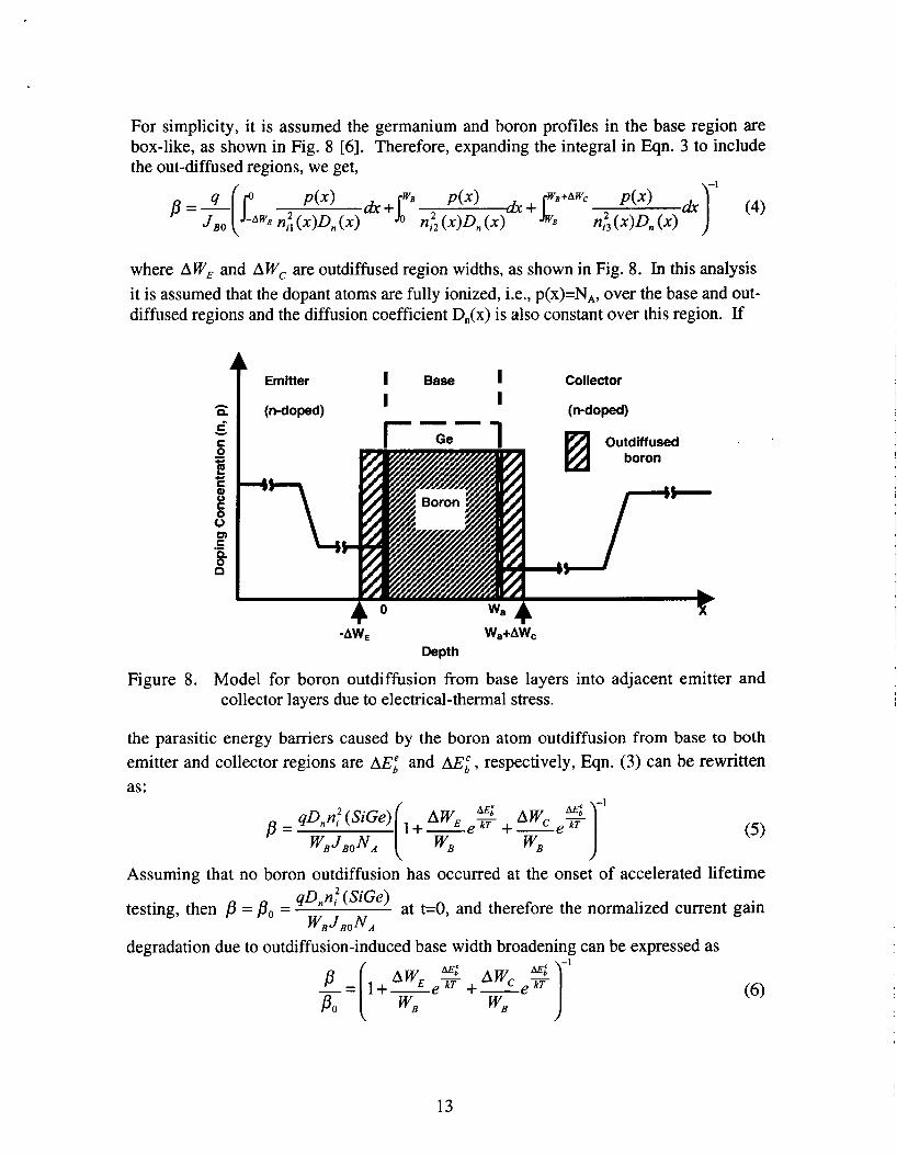
For simplicity, it is assumed the germanium and boron profiles in the base region are box-like, as shown in Fig. 8 [6]. Therefore, expanding the integral in Eqn. 3 to include the out-diffused regions, we get, . -1
where AWE and AWc are outdiffused region widths, as shown in Fig. 8. In this analysis it is assumed that the dopant atoms are fully ionized, Le., p(x)=N,, over the base and out- diffused regions and the diffusion coefficient D,(x) is also constant over this region. If
t Emitter I Base I Collector
(n-doped) I I I (n-doped)
L
-AWE W,+AW, Depth
Figure 8. Model for boron outdiffusion from base layers into adjacent emitter and collector layers due to electrical-thermal stress.
the parasitic energy barriers caused by the boron atom outdiffusion from base to both emitter and collector regions are A,?$ and Mi, respectively, Eqn. (3) can be rewritten as:
Assuming that no boron outdiffusion has occurred at the onset of accelerated lifetime qD,nf (SiGe)
testing, then P = Po = at t=O, and therefore the normalized current gain WE J d ' A
degradation due to outdiffusion-induced base width broadening can be expressed as
13
This equation is used to analyze the measured degradation of current gain p with stress time. In this work it is assumed that A W E = A W ~ = A L = ~ , where D, is the effective boron diffusion constant and t is the stress time. Thus the desired P(t) relation is obtained. D, can be expressed as [21]
where D,!’) and 0,”) are the diffusion coefficients of boron-neutral-point-defect pairs and of boron-positively-charged-point-defect pairs, respectively. E, is a bandgap a n d doping related activation energy. Originally, values of D:’) and 0;’) at our testing temperatures were extrapolated from those obtained in the literature [21] in this analysis. However, it is noted here that the diffusion coefficient, 0,“) , is enhanced by a factor of lo6 under bias conditions. Similar results were reported in the reliability tests of Be doped GaAs Esaki tunnel diodes [22]. The values of A,??; and A,??,’ are computed from the changes in Fermi levels produced by the boron outdiffusion. The decrease in the Sil- xGex bandgap, Mg, with composition is calculated from [23], [24], A,??g =0.85x. Finally, it is important to note that the heavy doping level in the base and out-diffused regions will cause bandgap narrowing, which can be approximately expressed by the empirical
equation [25], [26], A,??: = Eo ln[%), where E, =18 meV and N , =lo” cm”.
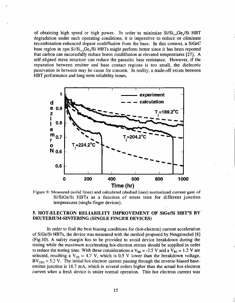
The calculated variation of current gain with stress time is shown in Fig. 9 alongside measured data for several stress temperatures. The agreement of the calculated results at the initial and the intermediate stages of each test run is fairly good, indicating that the device degradation at each testing temperature is due to boron outdiffusion. As mentioned before, the failure at the end of a test run is defined by different processes.
In formulating the diffusion model described above and utilizing it to analyze o u r data, it was found that the diffusion coefficient of boron-positively-charged-point-defect pairs (DY’) was enhanced by 6 orders under bias conditions. This anomalous behavior of the boron dopant is attributed to recombination-enhanced impurity diffusion (REID), which is reported in Be-doped GaAs [22]. For boron-doped npn Si/Si,-,Ge,/Si H B T s under forward active bias, electrons are injected from the emitter into the base. A fraction of the injected electrons will be captured by traps and recombination centers. The excess energy of the electrons is released non-radiatively and transferred to boron atoms, thereby enhancing their vibration and diffusivity. Because of the high efficiency of the non-radiative energy transfer, the enhancement of boron diffusivity should be m o r e significant than thermally activated diffusion. This explains why a control device, under the same thermal stress but without electrical stress, shows negligible DC current g a i n degradation. Similar results were reported from reliability tests on Be-doped GaAsIAlGaAs HBTs [19]. It is also appropriate to expect a more rapid degradation of Si/Si,-,Ge,/Si HBTs at higher stress current levels.
The reliability study offers valuable feedback to device heterostructure design. In practical applications, devices are usually driven at high current density for the purpase
14
of obtaining high speed or high power. In order to minimize Si/Si,-,Ge,/Si HBT degradation under such operating conditions, it is imperative to reduce or eliminate recombination-enhanced dopant outdiffusion from the base. In this context, a SiGeC base region in npn Si/Si,-,Ge,/Si HBTs might perform better since it has been reported that carbon can successfully reduce boron outdiffusion at elevated temperatures [27]. A self-aligned mesa structure can reduce the parasitic base resistance. However, if the separation between emitter and base contact regions is too small, the dielectric passivation in between may be cause for concern. In reality, a trade-off exists between HBT performance and long-term reliability issues.
1
d e 0.9 Z i I 0.8 a
0.7
0 N 0.6
r
0.6
I I I I
- - - calculation
-
-I --- --a - .I
0 200 400 600 800 1000 Time (hr)
Figure 9. Measured (solid lines) and calculated (dashed lines) normalized current gain of Si/SiGe/Si HBTs as a function of stress time for different junction temperatures (single-finger devices).
5. HOT-ELECTRON RELIABILITY IMPROVEMENT OF SiGe/Si HBT’S BY DEUTERILJM-SINTERING (SINGLE FINGER DEVICES)
In order to find the best biasing conditions for (hot-electron) current acceleration of SiGe/Si HBTs, the device was measured with the method proposed by Neugroschel [8] (Fig.10). A safety margin has to be provided to avoid device breakdown during the testing while the maximum accelerating hot-electron stream should be supplied in order to reduce the testing time. With these considerations a V,, = -3.5 V and a VBC = 1.2 V are selected, resulting a V,, = 4.7 V, which is 0.5 V lower than the breakdown voltage, BV,,, = 5.2 V. The initial hot electron current passing through the reverse-biased base- emitter junction is 18.7 mA, which is several orders higher than the actual hot-electron current when a fresh device is under normal operation. This hot electron current was
15
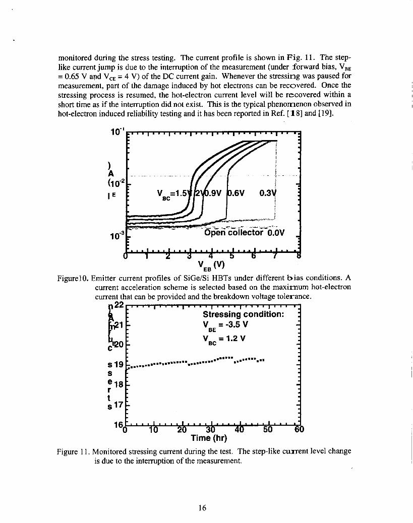
monitored during the stress testing. The current profile is shown in Fig. 1 1 . The step- like current jump is due to the interruption of the measurement (under forward bias, V,, = 0.65 V and V,, = 4 V) of the DC current gain. Whenever the stressing was paused for measurement, part of the damage induced by hot electrons can be recovered. Once the stressing process is resumed, the hot-electron current level will be recovered within a short time as if the interruption did not exist. This is the typical phenomenon observed in hot-electron induced reliability testing and it has been reported in Ref. [ 181 and [ 191.
Figurelo. Emitter current profiles of SiGe/Si HBTs under different b ias conditions. A current acceleration scheme is selected based on the maximum hot-electron current that can be provided and the breakdown voltage tolerance.
Stressing condition: v = -3.5 v
BE
C v =1.2v
BC
20 30 0 ' ' ' ' ' ' ' ' ' ' ' ' I I I ' ' bb' ' '
jj ' ' =-J Time (hr)
Figure 1 1. Monitored stressing current during the test. The step-like current level change is due to the interruption of the measurement.
16
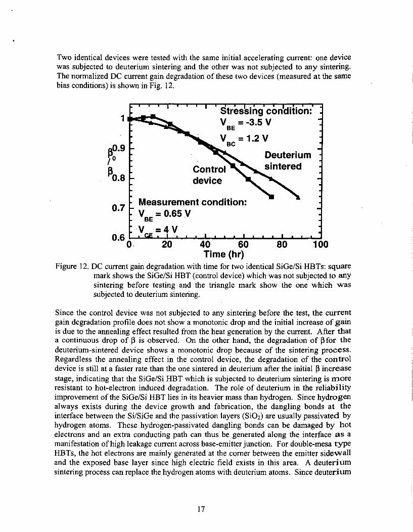
Two identical devices were tested with the same initial accelerating current: one device was subjected to deuterium sintering and the other was not subjected to any sintering. The normalized DC current gain degradation of these two devices (measured at the same bias conditions) is shown in Fig. 12.
1
I B;m9 B 0.8
0.7
1 1 1 ~ 1 1 1 [ 1 1 1 I I I I ,
Stres'sing' conhition: I
I
I
I
I
I I
I I - - Deuterium - - - I
I - - I I . I
I I - Measurement condition: I 1 V = 0.65.V BE
v = 4 v I 1 1 1 1 1 1 1 1 1 1 1 I l l l l l
20 40 60 80 100 0.6
0. Time (hr)
Figure 12. DC current gain degradation with time for two identical SiGe/Si HBTs: square mark shows the SiGe/Si HBT (control device) which was not subjected to any sintering before testing and the triangle mark show the one which was subjected to deuterium sintering.
Since the control device was not subjected to any sintering before the test, the current gain degradation profile does not show a monotonic drop and the initial increase of gain is due to the annealing effect resulted from the heat generation by the current. After that a continuous drop of p is observed. On the other hand, the degradation of pfor the deuterium-sintered device shows a monotonic drop because of the sintering process. Regardless the annealing effect in the control device, the degradation of the control device is still at a faster rate than the one sintered in deuterium after the initial p increase stage, indicating that the SiGe/Si HBT which is subjected to deuterium sintering is more resistant to hot-electron induced degradation. The role of deuterium in the reliability improvement of the SiGe/Si HBT lies in its heavier mass than hydrogen. Since hydrogen always exists during the device growth and fabrication, the dangling bonds at the interface between the Si/SiGe and the passivation layers (SiO2) are usually passivated by hydrogen atoms, These hydrogen-passivated dangling bonds can be damaged by hot electrons and an extra conducting path can thus be generated along the interface as a manifestation of high leakage current across base-emitter junction. For double-mesa type HBTs, the hot electrons are mainly generated at the comer between the emitter sidewall and the exposed base layer since high electric field exists in this area. A deuterium sintering process can replace the hydrogen atoms with deuterium atoms. Since deuterium
17
atoms are heavier than hydrogen atoms, they are more difficult to be removed by hot electrons and hence the degradation rate of the current gain becomes slower.
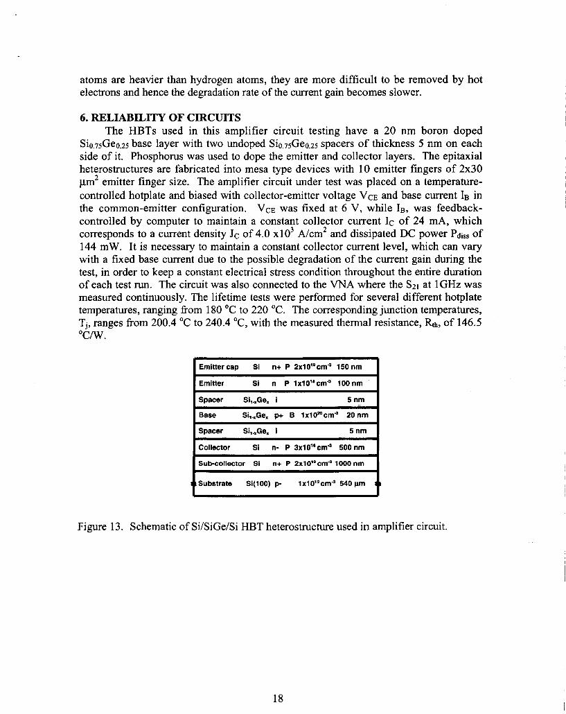
6. RELIABILITY OF CIRCUITS The HBTs used in this amplifier circuit testing have a 20 nm boron doped
Sio.7~Geo.25 base layer with two undoped Sio.75Geo.25 spacers of thickness 5 nm on each side of it. Phosphorus was used to dope the emitter and collector layers. The epitaxial heterostructures are fabricated into mesa type devices with 10 emitter fingers of 2x30 pm2 emitter finger size. The amplifier circuit under test was placed on a temperature- controlled hotplate and biased with collector-emitter voltage VCE and base current IB in the common-emitter configuration. VCE was fixed at 6 V, while IB, was feedback- controlled by computer to maintain a constant collector current IC of 24 mA, which corresponds to a current density JC of 4.0 x10³ A/cm2 and dissipated DC power Pdiss of 144 mW. It is necessary to maintain a constant collector current level, which can vary with a fixed base current due to the possible degradation of the current gain during the test, in order to keep a constant electrical stress condition throughout the entire duration of each test run. The circuit was also connected to the VNA where the S Z ~ at lGHz was measured continuously. The lifetime tests were performed for several different hotplate temperatures, ranging &om 180 OC to 220 OC. The corresponding junction temperatures, Tj, ranges from 200.4 "C to 240.4 OC, with the measured thermal resistance, %, of 146.5 OC/W.
I Base Si,,Ga, p+ B lxlOZOcmJ 20nm I
I Collector Si n- P 3 ~ 1 0 ' ~ c m ~ 500 nm I I Sub-collector SI n+ P 2 x 1 0 l ~ c m ~ 1000 nm I
I +Substrate Si(100) p 1xlO1*cmJ 540 pm
Figure 13. Schematic of Si/SiGe/Si HBT heterostructure used in amplifier circuit.
18
50 -
- 40
- 30 3
E w - 1 5 -Q
20 -
lo
30
25
20 63 2 6 cs
10
- 5
01 I I I I I I lo J o 0 50 100 150 200 250 300 350
Time(hr)
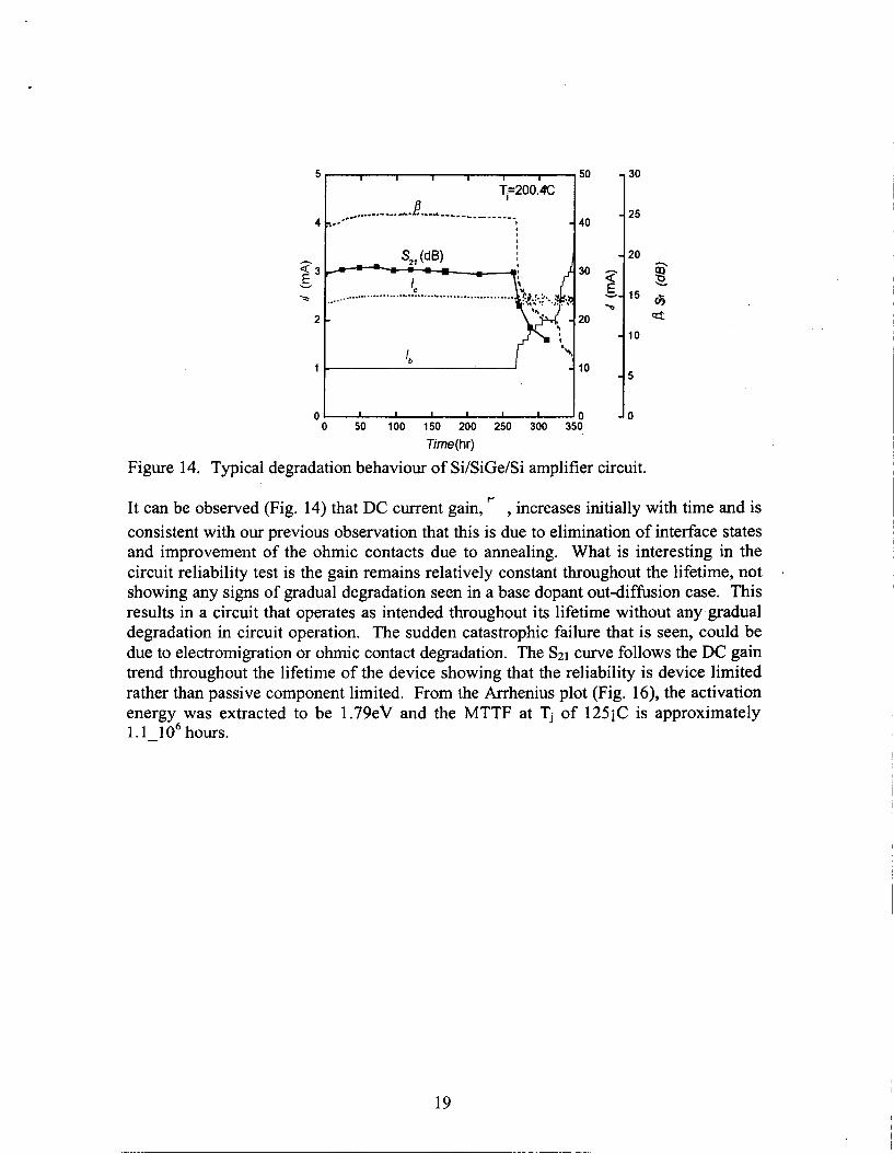
Figure 14. Typical degradation behaviour of Si/SiGe/Si amplifier circuit.
4
v
-p
2 -
1
r It can be observed (Fig. 14) that DC current gain, , increases initially with time and is consistent with our previous observation that this is due to elimination of interface states and improvement of the ohmic contacts due to annealing. What is interesting in the circuit reliability test is the gain remains relatively constant throughout the lifetime, not showing any signs of gradual degradation seen in a base dopant out-diffusion case. This results in a circuit that operates as intended throughout its lifetime without any gradual degradation in circuit operation. The sudden catastrophic failure that is seen, could be due to electromigration or ohmic contact degradation. The SZI curve follows the DC gain trend throughout the lifetime of the device showing that the reliability is device limited rather than passive component limited. From the Arrhenius plot (Fig. 16), the activation energy was extracted to be 1.79ev and the MTTF at Tj of 125iC is approximately 1.1 - 106hours.
T,=200:4c __.*... -.---.*-- P *--_--- .-__________
-.-I I - I , I 0
s,, (dB) I
2 3 + - 3 = - - - 'e .............................................. ._...
'b
19
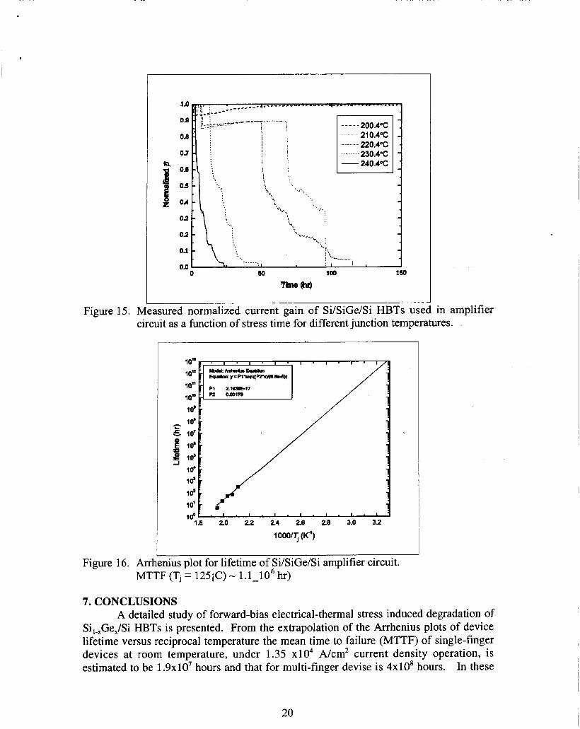
Figure 15. Measured normalized current gain of Si/SiGe/Si HBTs used in amplifier circuit as a function of stress time for different junction temperatures.
lOOO/T, (K')
Figure 16. Arrhenius plot for lifetime of Si/SiGe/Si amplifier circuit. MTTF (Tj = 125iC) - 1.1-106 hr)
7. CONCLUSIONS A detailed study of forward-bias electrical-thermal stress induced degradation of
Si,-,Ge,/Si HBTs is presented. From the extrapolation of the Arrhenius plots of device lifetime versus reciprocal temperature the mean time to failure (MTTF) of single-finger devices at room temperature, under 1.35 x 1 O4 A/cm2 current density operation, is estimated to be 1.9~10' hours and that for multi-finger devise is 4x10⁸ hours. In these
20
devices the gradual degradation and eventual failure are mainly caused by recombination enhanced boron outdiffusion from the base layer. Good agreement of the gradual degradation behavior is obtained with calculated results based on an analytical model which takes into account base dopant outdiffusion and the associated formation of parasitic energy barriers. Hot-electron reliability improvement of SiGe/Si HBT has been achieved by deuterium sintering. From the Arrhenius plot for SiGe/Si based amplifier circuit, with a current density Jc of 4.0 x10³ A/cm* and dissipated DC power Pdjss of 144 mW, the activation energy was extracted to be 1.79eV and the MTTF at Tj of 125iC is approximately 1. 1-106 hours. In these circuits, the gain remains relatively constant throughout its working lifetime resulting in a circuit that operates as intended without degradation in circuit operation. The circuit reliability is also shown to be device failure limited rather than passive component limited.
.
I
21
REFERENCES
[ l ] S. S. Iyer, G. L. Patton, J. M. C. Stork, B. S. Meyerson and D. L. Harame, “Heterojunction bipolar transistors using Si-Ge alloys,” ZEEE Trans. Electron Devices, vol. 36, pp. 2043-2064, 1989.
[2] B. Pej-inovi-, L. E. Kay, T.-W. Tang and D. H. Navon, “Numerical simulation and comparison of Si BJT’s and Si,-,Ge, HBT’s,” ZEEE Trans. Electron Devices, vol. 36, pp. 2129-2137, 1989.
[3] G. L. Patton, J. H. Comfort, B. S. Meyerson, E. F. Crabb , G. J. Scilla, E. de Fr sart, J. M. C. Stork, J. Y.-C. Sun, D. L. Harame and J. N. Burghartz, 75-GHz fT SiGe-base heterojunction bipolar transistors, IEEE Electron Device Lett., ~01.11, pp. 171-173, 1990.
[4] D. L. Harame, J. H. Comfort, J. D. Cressler, E. F. CrabbC, J. Y.-C. Sun, B. S. Meyerson and T. Tice, “Si/SiGe epitaxial-base transistors-Part I: Materials, physics, and circuits,” IEEE Trans. Electron Devices, vol. 42, pp. 455-467, 1995.
[SI A. Schiippen, U. Erben, A. Gruhle, H. Kibbel, H. Schumacher and U. Kkig, “Enhanced SiGe heterojunction bipolar transistors with 160 GHz-f,,,,” in ZEDM Tech. Dig., pp. 743-746, 1995.
energy barriers in SiGe HBT’s,” IEEE Electron Device Lett., vol. 12, pp. 486-488, 1991.
[7] E. J. Prinz, P. M. Garone, P. V. Schwartz, X. Xiao, and J. C. Sturm, “The effects of base dopant outdiffusion and undoped Si,-,Ge, junction spacer layers in Si/Si,- ,Ge,/Si heterojunction bipolar transistors,” IEEE Electron Device Lett., vol. 12, pp.
[6] J. W. Slotboom, G. Streutker, A. Pruijmboom and D. J. Gravesteijn, “Parasitic
42-44, 1991. [8] A. Neugroschel, C.-T. Sah, J. M. Ford, J. Steele, R. Tang, and C. Stein,
“Comparison of Time-to-Failure of GeSi and Si Bipolar Transistors,” IEEE Electron Device Lett., vol. 17, pp. 21 1-21 3, 1996.
[9] J. A. Babcock, A. J. Joseph, J. D. Cressler, and L. S. Vempati, “The effects of reverse-bias emitter-base stress on the cryogenic operation of advanced UHVICVD Si- and SiGe-base bipolar transistors,” in 1996 IEEE International Reliability Physics Proceedings. 34th Annual (Cat. No.96CH38525), pp.294-299, 1996.
“Elements of semiconductor-device reliability,” Proc. ZEEE, vol. 62, pp. 149- 168, 1974.
[ 1 11 F. H. Reynolds, “Thermally accelerated aging of semiconductor components,” Proc. ZEEE, vol. 62, pp. 212-222, 1974.
[12] R. F. Haythornthwaite, A. R. Molozzi, and D. V. Sulway, “Reliability assurance of individual semiconductor components,” Proc. ZEEE, vol. 62, pp. 260-273, 1974.
[13] J.-S. Rieh, L.-H. Lu, L. P. B. Katehi, P. Bhattacharya, E. T. Croke, G. E. Ponchak, and S. A. Alterovitz, “X- and Ku-band Amplifiers Based on Si/SiGe HBTs and Micromachined Lumped Components,” ZEEE Trans. Microwave Theory and Tech., vol. 46, pp. 685-694, 1998.
[ 101 C. G. Peattie, J. D. Adams, S. L. Carrell, T. D. George, and M. H. Valek,
22
[14] A. Samelis, “Analysis of the nonlinear characteristics of microwave power heterojunction bipolar transistors and optoelectronic integrated circuits,” Ph.D. dissertation, The University of Michigan, Ann Arbor, 1996.
[15] T. C. Chen, C. Kaya, M. B. Ketchen, and T. H. Ning, Reliability analysis of self- aligned bipolar transistor under forward active current stress, ZEDM Tech. Dig.,
[16] D. D.-L. Tang and E. Hackbarth, “Junction degradation in bipolar transistors and the reliability imposed constraints to scaling and design,” ZEEE Trans. Electron Devices, vol. 35, pp. 2101-2107, 1988.
[ 171 E. Hackbarth and D. D.-L. Tang, “Inherent and stress-induced leakage in heavily doped silicon junctions,” ZEEE Trans. Electron Devices, vol. 35, pp. 2108-21 18, 1988.
[ 181 R. A. Wachnik, T. J. Bucelot, and G. P. Li, “Degradation of bipolar transistors under high current stress at 300 K,” J. Appl. Phys., vol. 63, pp. 4734-4740, 1988.
[19] M. E. Hafizi, L. M. Pawlowicz, L. T. Tran, D. K. Umemoto, D. C. Streit, A. K. Oki, M. E. Kim and K. H. Yen, “Reliability analysis of GaAdAlGaAs HBT’s under forward current/temperature stress,” G d s IC Symposium, pp. 329-332, 1990.
[20] E. J. Prinz and J. C. Sturm, “Current gain-Early voltage products in heterojunction bipolar transistors with nonuniform base bandgaps,” ZEEE Electron Device Lett.,
[21] N. Moriya, L. C. Feldman, H. S. Luftman, C. A. King, J. Bevk and B. Freer, “Boron diffusion in Strained Si,,Ge, epitaxial layers, ” Phys. Rev. Lett., vol. 7 1,
[22] M. Uematsu, and K. Wada, “Recombination-enhanced impurity diffusion in Be- doped GaAs,” Appl. Phys. Lett., vol. 58, pp. 2015-2017, 1991.
[23] C. G. Van de Walle, R. M. Martin, “Theoretical calculations of heterojunction discontinuities in the Si/Ge system,” Phys. Rev. B vol. 34, pp. 5621-5634, 1986.
[24] J. C. Bean, “Silicon-based semiconductor heterostructures: Column IV bandgap engineering,” Proc. ZEEE, vol. 80, pp. 57 1-587, 1992.
[25] J. W. Slotboom and H. C. de Graaff, “Measurements of bandgap narrowing in Si bipolar transistors,” Solid State Electron. vol. 19, pp. 857-862, 1976.
[26] J. B. Kuo and T. C. Lu, “A fully analytical partitioned-charge-based model for linearly-graded SiGe-base heterojunction bipolar transistors,” Solid State Electron.
[27] L. D. Lanzerotti, J. C. Sturm, E. Stach, R. Hull, T. Buyuklimanli and C. Magee, “Suppression of boron transient enhanced diffusion in SiGe heterojunction bipolar transistors by carbon incorporation,” Appl. Phys. Lett., vol. 70, pp. 3 125-3 127, 1997.
pp. 650-653, 1986.
V O ~ . 12, pp. 661-663, 1991.
pp. 883-886, 1993.
V O ~ . 37, pp. 1561-1566, 1994.
23
Publication List:
1. Z. Ma, P. Bhattacharya, J.-S. Rieh, G . E. Ponchak, S . A. Alterovitz, E. T. Croke, Reliability of microwave SiGe/Si heterojunction bipolar transistors, ZEEE Microwave and Wireless Components Letters, Vol. 1 1, No. 10, pp. 401-403, October 2001.
2. Z. Ma, J.-S. Rieh, P. Bhattacharya, S. A. Alterovitz, G . E. Ponchak, E. T. Croke, Long- term reliability of Si/Sio.,Geo,3/Si HBTs from accelerated lifetime testing, ZEEE Topical Meeting on Silicon Monolithic Integrated Circuits in RF Systems, Ann Arbor, MI, September 12-14,2001, pp. 122-130.