Embed Size (px)
Citation preview

POUR L'OBTENTION DU GRADE DE DOCTEUR ÈS SCIENCES
acceptée sur proposition du jury:
Prof. H. Altug Yanik, présidente du juryProf. A. Radenovic, directrice de thèse
Prof. M. Krishnan , rapporteuseProf. R. Goldsmith, rapporteur
Prof. C. Degen , rapporteur
Nanoscale Magnetometry with Single Fluorescent Nanodiamonds Manipulated in an Anti-Brownian
Electrokinetic Trap
THÈSE NO 6972 (2016)
ÉCOLE POLYTECHNIQUE FÉDÉRALE DE LAUSANNE
PRÉSENTÉE LE 11 MARS 2016
À LA FACULTÉ DES SCIENCES ET TECHNIQUES DE L'INGÉNIEURLABORATOIRE DE BIOLOGIE À L'ÉCHELLE NANOMÉTRIQUE
PROGRAMME DOCTORAL EN PHOTONIQUE
Suisse2016
PAR
Metin KAYCI


2
Abstract
Studies on single-molecule spectroscopy and nanoscale detection have been remarkably driven by
an interest to reveal quantum and conformational states of single particles, the intra-molecular
dynamics and their response to physical observables hidden by ensemble level measurements. A
straightforward practice used in enhancing the signal from single particles is either to immobilize
them on an engineered substrate or to embed them in a solid matrix. Given that the biophysical
properties of the host environment introduce new perturbations and the particles will not behave
as in their native environment, such approaches are inefficient to reflect the real dynamics.
Therefore, recent advances in the field of single-molecule have led to a renewed interest in novel
trapping methods, increased efforts into the development of promising tools for extended
investigation, and the manipulation of solution-phase bio-molecules in real time. Despite the variety
of successful passive trapping techniques, precise manipulation through non-perturbative forces is
a big challenge for nano-sized particles. Such techniques either exert high power to the sample or
compel special operating conditions disturbing the native environment. Therefore, an active
trapping scheme guiding non-perturbative forces can break the trade-off between the particle size
and the excreted power.
This dissertation presents the development of an active trapping set-up using non-perturbative
electrokinetic feedback and demonstrates its performance on nano-sized single particles for aims in
biophysics. The essential theme is the engineering aspect of the technique, including the feedback
configurations for various fluidic devices, the corresponding particle tracking schemes and the
integration of the trapping platform to an integrated circuit pattern for advanced manipulation
aims. The second theme is on specialized single fluorescence nanodiamonds (FNDs) as scanning
magnetometer in fluidics. The implemented active trapping tool is employed for the manipulation
of a rotationally free single FND to detect the localized magnetic field through an optically detected
magnetic resonance (ODMR) spectrum. While the laser beam used in particle tracking can serve in
optical excitation, an external radio frequency (RF) source is not sufficient to achieve microwave
manipulation. Therefore, an RF antenna is designed to transmit the microwave signal to the
proximity of the trapping chamber for electron spin resonance (ESR) spectroscopy. A nanostage
positioning controller introduces scanning ability to the sample plane, in relative position of the
trapped particle, in order to map the distribution of the detected fields over a fluidic volume. As
FNDs are also sensitive to many other physical quantities, nanoscale single particle trapping and

3
diamond photonics linkages are realized in this work, which provide an outstanding alternative for
detection and imaging in complex fluidic environments that are closed to AFM-like physically
supported probes.
Keywords: Microfluidics, anti-Brownian electrokinetic trap (ABEL), electron spin resonance (ESR),
fluorescent nanodiamonds, nitrogen-vacancy, nanoscale magnetometry.

4
Résumé
Les études de spectroscopie à une seule molécule et la détection à l'échelle nano ont été
remarquablement dominées par un intérêt à révéler les états quantique ou conformationnels de
particules individuelles, la dynamique intramoléculaire et la réponse à certaines observables
physiques cachées par des mesures d'ensemble. Les particules individuelles, isolées, immobilisés
sur un substrat ou encastrées dans une matrice solide est une pratique simple utilisée pour
améliorer ce genre de mesures. Étant donné que les propriétés biophysiques de l'environnement
hôte introduisent de nouvelles perturbations et les particules ne se comporteront pas comme dans
leur environnement natif, ces approches sont inefficaces pour refléter la dynamique réelle. Par
conséquent, les progrès récents dans le domaine de la molécule unique ont conduit à un regain
d'intérêt dans de nouvelles méthodes de piégeage et de grands efforts ont été consacrés à
l'élaboration d'outils prometteurs pour l’enquête approfondie et la manipulation des bio-molécules
en phase solution et en temps réel. Bien qu'une grande variété de techniques de piégeages passifs
ont été démontrés, la manipulation précise grâce à des forces non-perturbatrices est un grand défi
pour les particules de taille nanométrique. Ces techniques exercent soit une puissance élevée à
l'échantillon ou impliquent des conditions particulières perturbant l'environnement natif. Au lieu de
cela, un système de piégeage actif guidant des forces non perturbatrices peut briser le compromis
entre la taille des particules et la puissance excrétée.
Cette thèse présente le développement d'une installation de piégeage actif en utilisant des feedback
électro cinétique non perturbateurs et démontre sa performance sur les particules individuelles de
taille nanométrique pour objectifs biophysique. Le thème essentiel est l'aspect technique, y compris
les configurations de feedback pour divers dispositifs fluidiques, les systèmes de suivi des particules
correspondantes et l'intégration de la plate-forme de piégeage à un modèle de circuit intégré pour
des installations de manipulation. Le deuxième thème est les nano diamants fluorescent (FNDS) en
tant que magnétomètre en fluidique. L’outil de piégeage actif est mis en œuvre dans la manipulation
d'un seul FND libre en rotation pour détecter le champ magnétique local par résonance magnétique
optiquement détecté (ODMR). Alors que le faisceau laser utilisé dans le suivi des particules peut
servir à une excitation optique, une fréquence radio externe (RF) n’est pas suffisante pour atteindre
la manipulation de micro-ondes. Par conséquent, une antenne RF est conçue pour transmettre le
signal hyperfréquence à la proximité de la chambre de piégeage pour une résonance de spin
électronique (ESR) par spectroscopie. Un dispositif de positionnement nano introduit la capacité de

5
balayage de l’échantillon, et donc également la position relative de la particule piégée, pour
cartographier la distribution des champs détectés sur un volume de fluide. Comme FNDS sont
également sensibles à beaucoup d'autres grandeurs physiques, le piégeage des particules
nanométrique lié à la photonique de diamant réalisée dans ce travail fournit une excellente
alternative pour la détection et l'imagerie dans des environnements fluidiques complexes qui sont
fermés aux sondes purement physique comme l’AFM.
Mots-clés: Microfluidique, anti-Brownien électrocinétique trappe (ABEL), résonance de spin
électronique (RSE), nanodiamants fluorescents, vacance d'azote, magnétométrie à l'échelle
nanométrique.

6
Acknowledgements
First of all, I would like to thank my thesis director Prof. Aleksandra Radenovic who gave me the
opportunity to pursue a PhD in her lab and provided a comfortable research environment. She
always encouraged me to implement creative ideas into my work. It would not have been possible
to complete this work without her guidance, and support.
I would like to thank the jury members of my thesis committee for taking the time to read and giving
constructive feedbacks.
I would like to thank all my colleagues for the nice atmosphere in the lab and lots of helpful advices.
Finally, I would like to present my special thanks to my family for their love, encouragement and
continuous support. I owe them a lot.

7
Thesis Outline
Chapter 1 presents a detailed description of the set-up used for single particle trapping in
microfluidics. The Brownian motion and the counteracting forces generated in microfluidics for
position control are briefly summarized. Given that nanoscale particles are diffusing very fast and
camera-based solutions are not efficient for monitoring, a laser-guided scheme is used for positon
detection. The scanning excitation, the confocal detection and the digital filter employed in
transversal position estimation are the main issues focused in this chapter.
Chapter 2 is content reproduced verbatim from a submitted book chapter on single fluorescence
nanodiamonds (FNDs), which reviews studies on nitrogen vacancy defects embedded in FNDs and
their applications in mapping and sensing physical quantities. The working principles of the
applications are illustrated through the outstanding spin and optical properties that the defect
introduces. The manipulation techniques proposed in the literature are compared to the one
employing electrokinetic forces.
Chapter 3 is content reproduced verbatim from a published work on three-dimensional single
particle manipulation. It presents the hybrid approach used in positon detection and the novel
microfluidic configuration used for three-dimensional feedback. It is shown that the off-focus
fluorescence profile of a nanoscale particle can be image-processed to extract its axial position.
Then, the corresponding feedback can be applied through a cascaded thin PDMS layer coupling the
electrokinetic forces into the axial dimension.
Chapter 4 is content reproduced verbatim from a published work on single FNDs in ABEL trap. It is
shown that ABEL trap technique is compatible to electron spin resonance (ESR) experiments carried
on single FNDs. The design of a radio frequency antenna for microwave excitation and its integration
to the trapping platform is presented. With the link provided in this work, it is demonstrated that
sensing and imaging capabilities of single FNDs can be exploited in environments where other
manipulation techniques are not functional. The approach is validated through magnetic field
sensing in closed microfluidics.
Chapter 5 summarizes the complete work done in this PhD thesis and puts it into perspective by
describing possible future directions.
8
Contents Abstract ............................................................................................................................................................................. 2
Résumé ............................................................................................................................................................................. 4
Acknowledgements ........................................................................................................................................................... 6
Thesis Outline .................................................................................................................................................................... 7
1. Introduction ................................................................................................................................................................. 10
1.1 Brownian Motion ............................................................................................................................................. 10
1.2 Manipulation Techniques for Aqueous Dispersions ........................................................................................ 12
1.3 Electrokinetic Forces in Microfluidics .............................................................................................................. 15
1.4 Anti-Brownian Electrokinetic (ABEL) Trap ....................................................................................................... 16
1.4.1 Excitation Optics.................................................................................................................................. 17
1.4.2 Detection Optics .................................................................................................................................. 19
1.4.3 Kalman Filter ....................................................................................................................................... 19
2. Fluorescent Nanodiamonds in Biological and Biomedical Imaging and Sensing ............................................................ 22
2.1 Introduction ..................................................................................................................................................... 22
2.2 General Properties of Fluorescent Nanodiamonds as Biomarkers and Biosensors ......................................... 23
2.3 Nanoscale Imaging of Biological Systems with NV-centers Hosted in Nanodiamonds .................................... 29
2.4 Super-resolution Microscopy with Fluorescent Nanodiamonds...................................................................... 30
2.5 Nanoscale Sensing of Biological Systems with NV centers Hosted in Nanodiamonds ..................................... 36
2.6 Manipulation Techniques ................................................................................................................................ 37
2.6.1 Scanning Probe .................................................................................................................................... 37
2.6.2 Optical Tweezers ................................................................................................................................. 39
2.6.3 ABEL Trap ............................................................................................................................................ 40
2.7 Conclusion ....................................................................................................................................................... 42
3. Single Fluorescent Nanodiamond in a Three-Dimensional ABEL Trap ........................................................................... 43
3.1 Abstract ........................................................................................................................................................... 43
3.2 Introduction ..................................................................................................................................................... 43
3.3 Microfluidic Cell ............................................................................................................................................... 45
3.4 Three-Dimensional Position Tracking .............................................................................................................. 46
3.5 Fluorescent Nanodiamond Trap ...................................................................................................................... 48
3.6 Conclusion ....................................................................................................................................................... 49
3.7 Supporting Information ................................................................................................................................... 50
3.7.1 Image Processing Based Position Estimation for Axial Dimension ...................................................... 50
3.7.2 Kalman-Filter Based Position Estimation in the Transverse Plane ...................................................... 51
3.7.3 Microfluidic Cell Fabrication................................................................................................................ 51
4. Electron Spin Resonance of Nitrogen-Vacancy Defects Embedded in Single Nanodiamonds in an ABEL Trap ................ 53
4.1 Abstract ........................................................................................................................................................... 53

9
4.2 Introduction ..................................................................................................................................................... 53
4.3 Results and Discussion ..................................................................................................................................... 55
4.4 Materials and Methods ................................................................................................................................... 61
4.4.1 Fluorescent Nanodiamond (FND) ........................................................................................................ 61
4.4.2 The RF Circuit ...................................................................................................................................... 61
4.4.3 Kalman-Filter ....................................................................................................................................... 62
4.4.4 Scanning Pattern ................................................................................................................................. 63
4.4.5 RF Circuit Integrated Microfluidic Cell Fabrication .............................................................................. 63
4.5 Conclusion ....................................................................................................................................................... 63
4.6 Supporting Information ................................................................................................................................... 64
4.6.1 Inspection of Laser Guided Position Estimates ................................................................................... 64
4.6.2 PDMS on SU8 Master .......................................................................................................................... 65
4.6.3 RF Circuit on Cover Glass ..................................................................................................................... 67
4.6.4 ESR Spectrum of a Rotationally Diffusing FND with NV Defects.......................................................... 68
5. Conclusion and Outlook ............................................................................................................................................... 69
List of Acronyms .............................................................................................................................................................. 72
References ....................................................................................................................................................................... 74
Curriculum Vitae .............................................................................................................................................................. 79

10
1. Introduction
Positon control and manipulation of a single particle in solution phase plays a major role for studying
fundamental problems in various fields of research. For instance, through the changes in the
fluorescence signal, one can investigate the inner dynamics of a particle that is not resolvable in
ensemble level averaging. Given that the conformational states of a protein determine its
functionality and contribute to the fluorescence profile, single particle manipulation provides a
remarkable tool for cell biology and pharmacological research. Furthermore, by position control of
a sensitive particle in a local volume, one can resolve the physical quantities in the environment and
map the distributions through the particle response. In other words, with the scanning ability a
functional nanoscale particle can act as biophysical sensor resolving environmental characteristics.
With these motivations, there are a number of techniques exploiting different schemes for the
manipulation of single particles, see section 1.2. Unfortunately, such techniques fail to provide
precise measurements on nanoscale particles either due to the restrictions on particle properties
and operating conditions or due to the perturbations they introduce to the environment. Therefore,
the first objective of this PhD work aims to realize an active trapping platform cancelling the
Brownian motion through the electrokinetic forces in microfluidics. Precise single particle tracking
at high temporal resolution and following active control are the main approaches used for the
manipulation, see section 1.3. Unlike passive approaches, the platform applies electrokinetic forces
in a smart manner, so that the manipulation is not perturbative and operational on all optically
traceable nanoparticles in solution.
Once the position control has been achieved, we employed the platform in the manipulation of
nitrogen vacancy (NV) centres in single fluorescent nanodiamonds (FNDs) for scanning
magnetometry application. Non-perturbative manipulation of nanoscale particles without any
physical support and single particle level position control in closed fluidics are the key advantages
over the other approaches used in single FNDs manipulation, see section 2.6.
1.1 Brownian Motion
Although the discovery of Brownian motion is attributed to Robert Brown for his work on pollen
grains suspended in water [1], he was not the first to observe the phenomenon. Jan Ingenhousz
reported the fluctuations in motion of suspended coal dust particles in 1765. The stochastic
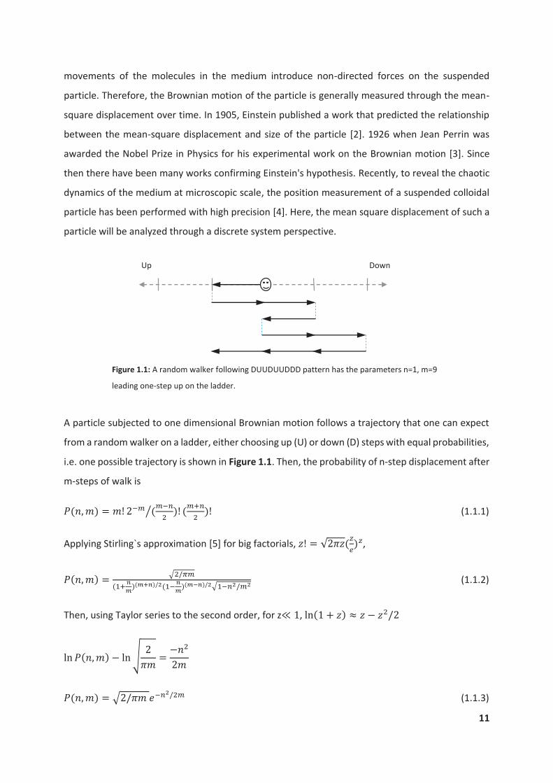
11
movements of the molecules in the medium introduce non-directed forces on the suspended
particle. Therefore, the Brownian motion of the particle is generally measured through the mean-
square displacement over time. In 1905, Einstein published a work that predicted the relationship
between the mean-square displacement and size of the particle [2]. 1926 when Jean Perrin was
awarded the Nobel Prize in Physics for his experimental work on the Brownian motion [3]. Since
then there have been many works confirming Einstein's hypothesis. Recently, to reveal the chaotic
dynamics of the medium at microscopic scale, the position measurement of a suspended colloidal
particle has been performed with high precision [4]. Here, the mean square displacement of such a
particle will be analyzed through a discrete system perspective.
A particle subjected to one dimensional Brownian motion follows a trajectory that one can expect
from a random walker on a ladder, either choosing up (U) or down (D) steps with equal probabilities,
i.e. one possible trajectory is shown in Figure 1.1. Then, the probability of n-step displacement after
m-steps of walk is
(1.1.1)
Applying Stirling`s approximation [5] for big factorials, ,
(1.1.2)
Then, using Taylor series to the second order, for z ,
(1.1.3)
Up Down
Figure 1.1: A random walker following DUUDUUDDD pattern has the parameters n=1, m=9
leading one-step up on the ladder.
12
Provided that each step leads to a distance change of in a time bin of , the equation can be
expressed in a continuous form probability density,
,
(1.1.4)
where is the diffusion constant of the walker. Given that the random walks along
orthogonal dimensions are uncorrelated, the mean-square displacement of 1D and 3D walk
are and , respectively. As Einstein-Smoluchowski’s equation relates, the
diffusion constant to the size of the suspended particle and the viscosity of medium , one can
predict the mean-square displacement of a particle within a given time period.
(1.1.5)
1.2 Manipulation Techniques for Aqueous Dispersions
Several manipulation techniques for single FNDs trapping and spatial scanning are compared in
section 2.6. In this section, the working principle of the manipulation techniques that are used for
general tasks will be provided.
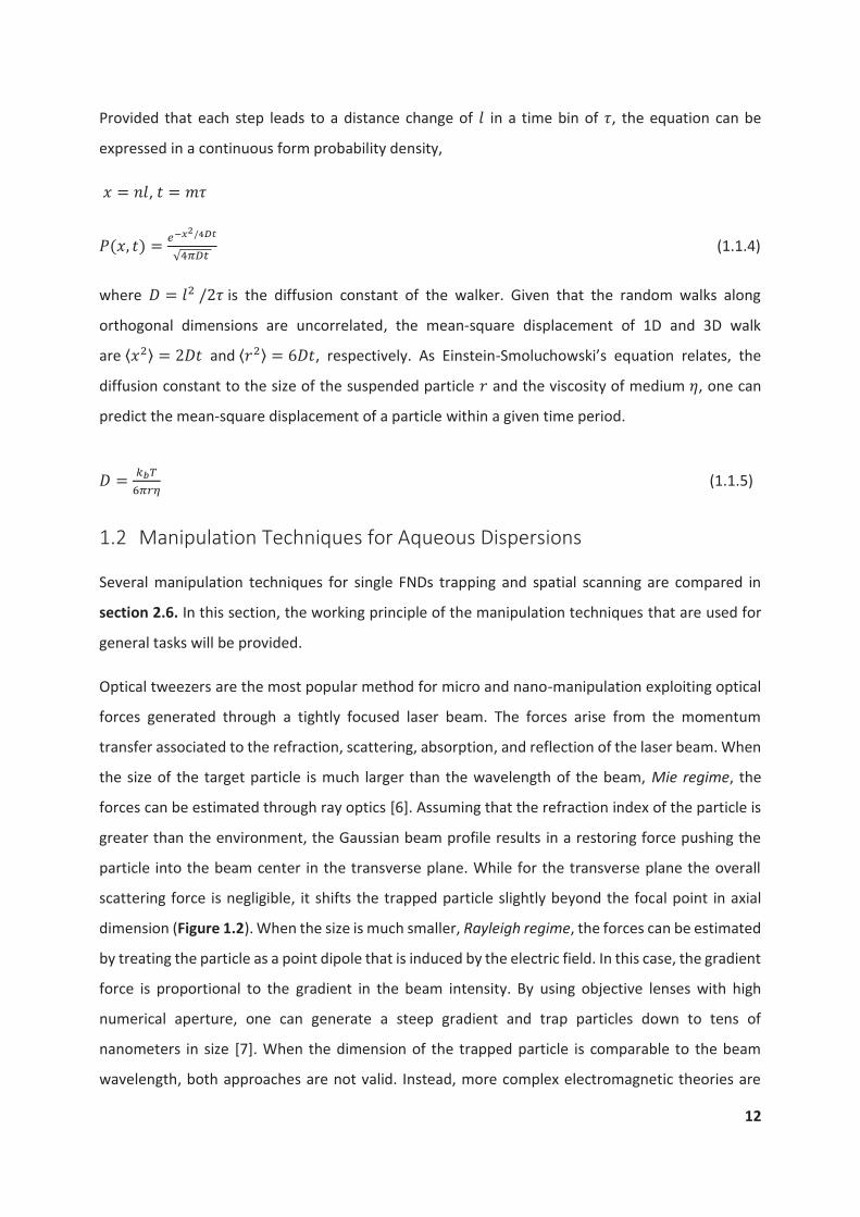
Optical tweezers are the most popular method for micro and nano-manipulation exploiting optical
forces generated through a tightly focused laser beam. The forces arise from the momentum
transfer associated to the refraction, scattering, absorption, and reflection of the laser beam. When
the size of the target particle is much larger than the wavelength of the beam, Mie regime, the
forces can be estimated through ray optics [6]. Assuming that the refraction index of the particle is
greater than the environment, the Gaussian beam profile results in a restoring force pushing the
particle into the beam center in the transverse plane. While for the transverse plane the overall
scattering force is negligible, it shifts the trapped particle slightly beyond the focal point in axial
dimension (Figure 1.2). When the size is much smaller, Rayleigh regime, the forces can be estimated
by treating the particle as a point dipole that is induced by the electric field. In this case, the gradient
force is proportional to the gradient in the beam intensity. By using objective lenses with high
numerical aperture, one can generate a steep gradient and trap particles down to tens of
nanometers in size [7]. When the dimension of the trapped particle is comparable to the beam
wavelength, both approaches are not valid. Instead, more complex electromagnetic theories are

13
used for the estimation of the optical forces [8]. Despite the functionality of optical tweezers for a
wide range of particle sizes, they do have some drawbacks. For instance, the high optical power
required for a stable trapping can result in photo-damage or local heating in bio-samples [9].
Furthermore, as the generated optical forces are passive, any dielectric particle can be trapped.
Therefore, manipulation at the single particle level requires extremely low concentrations.
Figure 1.2: Schematic of optical tweezers illustrating the principle of trapping through ray optics. a) As the intensity of
the refracting beam is larger in the center, the imparted momentum moves the particle towards the center in the
transverse plane. b) The particle moves slightly above the focal point in the axial dimension due to the reflection
and the refraction components.
Even though optical tweezers are not practical due to the excreted power and size trade-off,
electrostatic trapping provides another option [10]. In this technique the trapping resolution is
limited by the charge state of the target particle rather than its size. Although this configuration is
not feasible for three-dimensional active positioning and the trapping performance depends on
buffer characteristics, it provides an outstanding option for nanoscale particle sorting into high
density arrays and single particle level analysis for a long period of time.
Standing waves provide yet another possibility for micro-manipulation. In this technique, particles
are trapped in low pressure nodes that are generated by interdigital transduces. Recently, two-
dimensional manipulation of single particles has been demonstrated [11]. The radiation force of
plane waves depends on the target size; hence, filtering and sorting applications [12] are also
possible. In contrast to optical tweezer, acoustic tweezers that employ standing waves are not
sourcing local heating or photo-damage, so long term manipulation is possible. Although this
approach is biocompatible and non-invasive, it is not viable for nanoscale manipulation. Further,
excluding the complex versions, precise manipulation on an arbitrary path is not practical.
14
Hydrodynamic actuation is a powerful approach for the manipulation of arbitrary particles that do
not possess any specific chemical or physical properties. Recently, manipulation of submicron single
particles has been demonstrated through active hydrodynamic flow control in microfluidics [13].
The difficulty in precise flow control is the main drawback of the technique. Also, the chip valves
used in the active feedback bring additional complexity to the fabrication process of the
microfluidics.
Although not very popular, aqueous Paul trapping is another alternative for manipulation. Basically,
the Brownian motion of the target particle is suppressed through DC and radio frequency voltages
that introduce a focusing and defocusing potential well for the particle. Recently, nanoscale
manipulation of single particles has been demonstrated in aqueous [14]. The complex fabrication
process of the device and instability of three-dimensional positioning are the main drawbacks of the
technique.
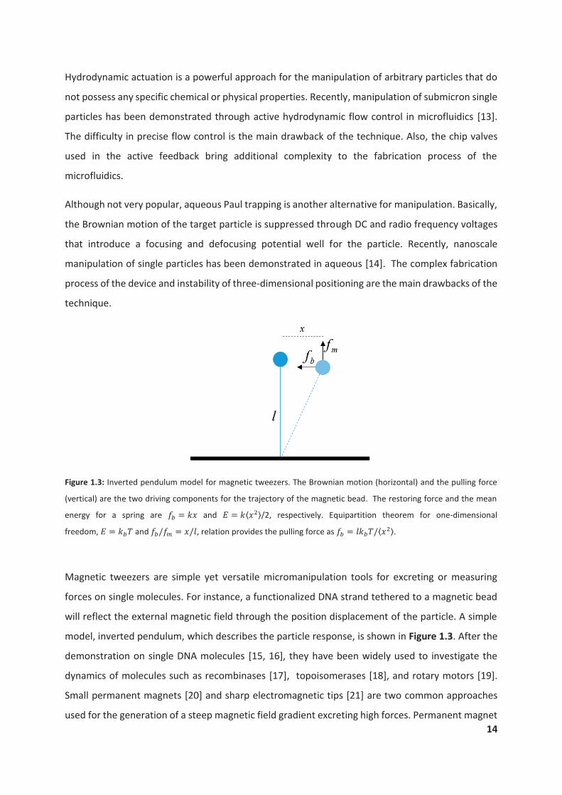
Figure 1.3: Inverted pendulum model for magnetic tweezers. The Brownian motion (horizontal) and the pulling force
(vertical) are the two driving components for the trajectory of the magnetic bead. The restoring force and the mean
energy for a spring are and /2, respectively. Equipartition theorem for one-dimensional
freedom, and , relation provides the pulling force as .
Magnetic tweezers are simple yet versatile micromanipulation tools for excreting or measuring
forces on single molecules. For instance, a functionalized DNA strand tethered to a magnetic bead
will reflect the external magnetic field through the position displacement of the particle. A simple
model, inverted pendulum, which describes the particle response, is shown in Figure 1.3. After the
demonstration on single DNA molecules [15, 16], they have been widely used to investigate the
dynamics of molecules such as recombinases [17], topoisomerases [18], and rotary motors [19].
Small permanent magnets [20] and sharp electromagnetic tips [21] are two common approaches
used for the generation of a steep magnetic field gradient excreting high forces. Permanent magnet

15
configuration is very simple and useful for constant force experiments, but it lacks the ability of wide
range positioning. Conversely, multiple electromagnet configuration [22] is a promising approach
for three-dimensional manipulation as the generated force and its direction can be controlled
through the current modulation and switching for active feedback. However, high driving current
on electromagnets leads to hysteresis and heating that requires an active cooling system. Also, all
magnetic tweezers’ configurations are functional only if the target particle is paramagnetic or
tethered to a paramagnetic particle.
Ultimately, all the techniques mentioned above either demand specific conditions for operation or
are not functional for three-dimensional positioning at single particle level.
1.3 Electrokinetic Forces in Microfluidics
Electrophoresis and electroosmotic forces are the main components contributing to the
electrokinetic mobility of a particle in aqueous medium when a potential is applied through the
microfluidics (Figure 1.4).
For a charged particle, the balance between the Coulomb force and the drag force determines the
electrophoresis velocity. For spherical objects, , , where is
the electric field, is the permittivity of free space, is the surface potential, is the viscosity, is
the dielectric constant of the fluid, is the velocity, and is the radius of the particle. Then, the
electrophoresis mobility is which is known as Huckel's formula [23]. This
phenomena has been extensively used for amino acid-protein separation [24, 25], drug analysis [26,
27], and DNA sequencing [28, 29].
Figure 1.4: a) The forces contributing to the electrophoresis mobility. b) As a result of the applied potential, the
mobile ions accumulated on negatively charged microfluidic surface generate a bulk flow.

16
When a potential is applied across the channel, a double layer of ions are formed on the charged
microfluidic surface. Unlike the inner layer, the outer layer has mobile ions generating a bulk flow
in the channel. This actuation introduces the electroosmotic mobility for the particle in the medium.
Let be the charge density on the microfluidics surface. Then, the electric force per unit area on
ions at Debye length, , is where . The viscosity force per unit area at
is given as . In steady state, the equality of these two components provides the
mobility , which is known as Smoluchowski's formula [30]. Recently, micro pumps for
fluid cooling [31] and fluid mixing [32] have been proposed as potential applications employing
electroosmotic control.
The overall mobility is generalized through Henry`s function [33] by scaling it with particle size and
Debye length ratio, . The main conclusion here is that for a given particle size and
buffer viscosity, the mobility is constant. This allows a linear electrokinetic control over the position
of a nanoscale particle. Instead of theoretical calculations, the mobility parameter can be extracted
easily by monitoring the position response of such a particle on an applied electric field strength.
1.4 Anti-Brownian Electrokinetic (ABEL) Trap
The Anti-Brownian elelctrokinetic trap (ABEL trap) is a tool first invented by Adam Cohen and W.E.
Moerner to manipulate single fluorescent molecules in solution phase [34-36]. As the name
suggests, the objective is to cancel the Brownian motion by electrokinetic forces. The main challenge
of such an active trapping tool is to track the Brownian motion of a nanoscale particle over a very
short time period, where the particle is not able to escape. Since we are not interested in the
imaging of a fluidic sample, but the tracking of a diffusing single particle and the mean square
displacement of nanoscale particles is very high camera-based solutions are not practical. Instead,
a scanning excitation laser beam with a very fast single photon counting module (SPCM) can provide
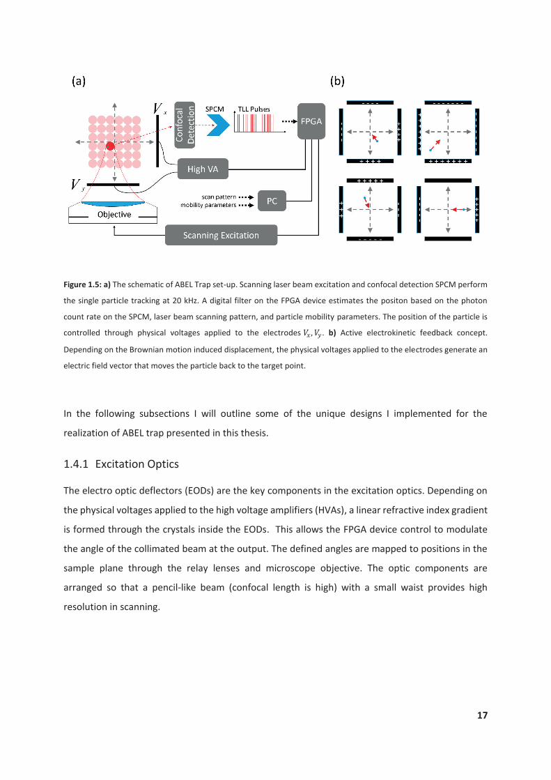
the required tracking frequency. The working principle of a two-dimensional ABEL trap set-up is
schematized in Figure 1.5. Basically, it consists of a scanning excitation, a confocal detection and a
digital filter on a field programmable gate array (FPGA) device performing the position estimation
and active feedback.
17
Figure 1.5: a) The schematic of ABEL Trap set-up. Scanning laser beam excitation and confocal detection SPCM perform
the single particle tracking at 20 kHz. A digital filter on the FPGA device estimates the positon based on the photon
count rate on the SPCM, laser beam scanning pattern, and particle mobility parameters. The position of the particle is
controlled through physical voltages applied to the electrodes . b) Active electrokinetic feedback concept.
Depending on the Brownian motion induced displacement, the physical voltages applied to the electrodes generate an
electric field vector that moves the particle back to the target point.
In the following subsections I will outline some of the unique designs I implemented for the
realization of ABEL trap presented in this thesis.
1.4.1 Excitation Optics
The electro optic deflectors (EODs) are the key components in the excitation optics. Depending on
the physical voltages applied to the high voltage amplifiers (HVAs), a linear refractive index gradient
is formed through the crystals inside the EODs. This allows the FPGA device control to modulate
the angle of the collimated beam at the output. The defined angles are mapped to positions in the
sample plane through the relay lenses and microscope objective. The optic components are
arranged so that a pencil-like beam (confocal length is high) with a small waist provides high
resolution in scanning.

18
Figure 1.6: The optics performing excitation in scanning mode. The angles introduced with the EODs are mapped to
linear positions in the sample plane through the relay lenses.
The beam waist formed through a microscope objective is , where defines the
subtended angle [37] at the focus point and is the wavelength of the beam. A beam with a waist
of entering the objective sets the angle as , where states the objective focal length
(see Figure 1.7). For a microscope objective with magnification , where defines the
focal length of the tube lens. A beam waist of passing through the relay lenses with focal length
of and rescales as . While a very small beam waist is possible with the given
parameters the high confocal length [38] requirement for a pencil-like beam is an important
limiting factor . Since EODs are operating at high physical voltages, HVAs are used to
amplify the output voltages of the FPGA device. Then, the deflection angle is , where is
a constant is the gain of HVAs and is the analog output of the FPGA device used for control. The
deflection angle is converted to a position in the sample plane through the geometry provided by
the intermediate optics, , where is the distance to the first relay lens (Figure
1.6).
Figure 1.7: The confocal beam in the sample plane. The beam waist is a function of subtended angle.

19
With the specification given above, a laser beam with a waist of ≈0.8 μm and confocal length of ≈7
μm is used in this work to perform high resolution scanning over an area up to 20x20 μm2 in the
sample plane.
1.4.2 Detection Optics
Figure 1.8: The optic train performing confocal detection of the fluorescent particle in the sample plane.
The fluorescence signal collected by the microscope objective passes through a bandpass filter and
focused to the 1st image plane for further filtering (see Figure 1.8). The confocal detection of the
fluorescence signal emitted from the target particle is managed through two optical components.
One is the pinhole that selects a small area in the sample plane proportional to its size. The selected
area with a pinhole of size is . Furthermore, it rejects the off-plane auto fluorescence
signal in the background, enhancing signal to the noise ratio. The second component filtering the
environmental noise is fiber optic channel connected to the single photon counting module (SPCM).
The signal survived in the optical fiber core and directed to the SPCM is limited to the NA of the fiber
channel.
1.4.3 Kalman Filter
The Kalman filter [39] is one of the most popular algorithms extensively used in many different
disciplines for information processing, estimation, and control. One of its famous applications was
the spacecraft navigation for the Apollo project in 1960. Recently, it has been used for weather
prediction [40], face recognition [41], curve fitting [42], and mobile robot localization [43]. The
recursive nature of the algorithm makes it very powerful for real time applications. The information
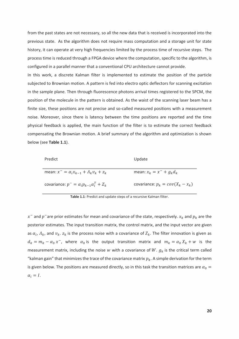
20
from the past states are not necessary, so all the new data that is received is incorporated into the
previous state. As the algorithm does not require mass computation and a storage unit for state
history, it can operate at very high frequencies limited by the process time of recursive steps. The
process time is reduced through a FPGA device where the computation, specific to the algorithm, is
configured in a parallel manner that a conventional CPU architecture cannot provide.
In this work, a discrete Kalman filter is implemented to estimate the position of the particle
subjected to Brownian motion. A pattern is fed into electro optic deflectors for scanning excitation
in the sample plane. Then through fluorescence photons arrival times registered to the SPCM, the
position of the molecule in the pattern is obtained. As the waist of the scanning laser beam has a
finite size, these positions are not precise and so-called measured positions with a measurement
noise. Moreover, since there is latency between the time positions are reported and the time
physical feedback is applied, the main function of the filter is to estimate the correct feedback
compensating the Brownian motion. A brief summary of the algorithm and optimization is shown
below (see Table 1.1).
Predict Update
mean:
covariance:
mean:
covariance:
Table 1.1: Predict and update steps of a recursive Kalman filter.
and are prior estimates for mean and covariance of the state, respectively. and are the
posterior estimates. The input transition matrix, the control matrix, and the input vector are given
as , , and . is the process noise with a covariance of . The filter innovation is given as
where is the output transition matrix and is the
measurement matrix, including the noise with a covariance of . is the critical term called
“kalman gain” that minimizes the trace of the covariance matrix . A simple derivation for the term
is given below. The positions are measured directly, so in this task the transition matrices are
.
21
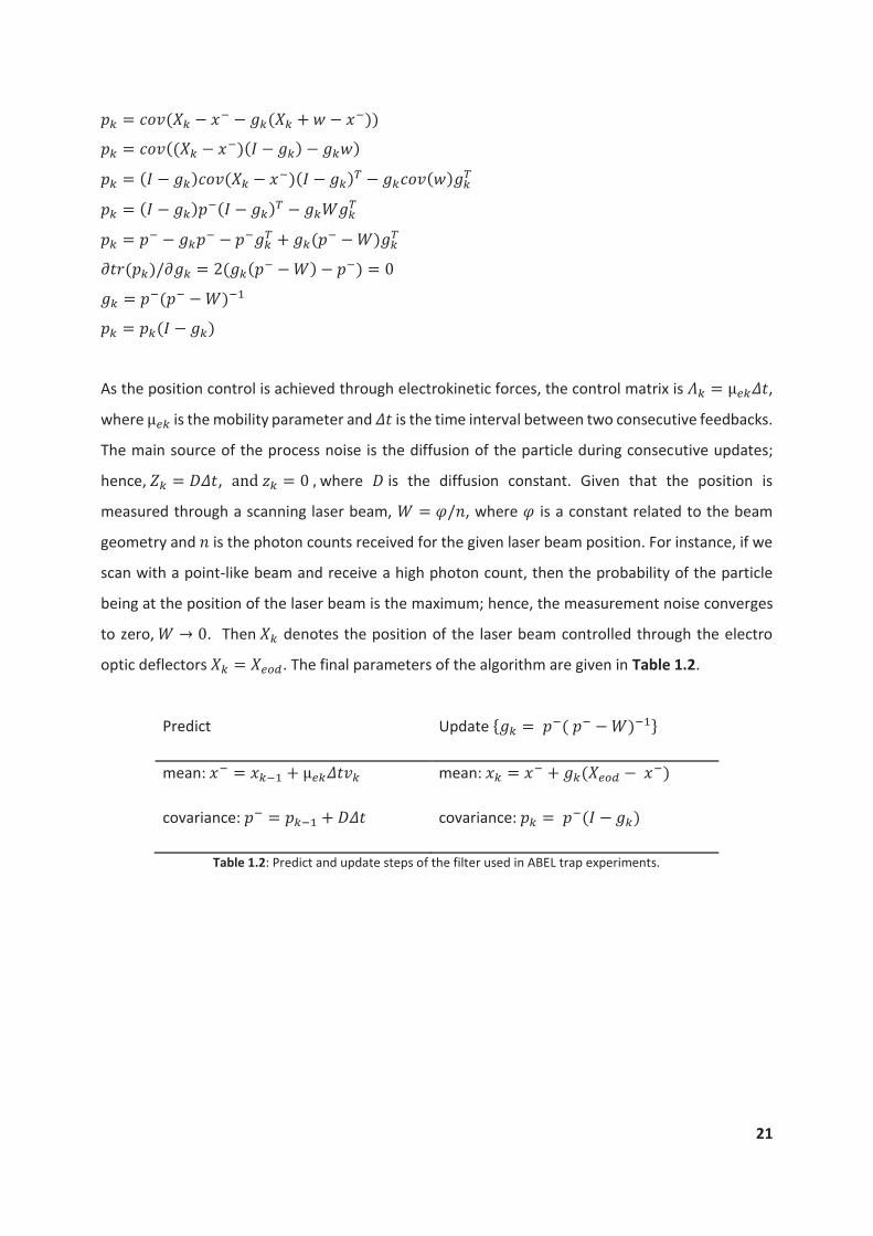
As the position control is achieved through electrokinetic forces, the control matrix is ,
where is the mobility parameter and is the time interval between two consecutive feedbacks.
The main source of the process noise is the diffusion of the particle during consecutive updates;
hence, , where is the diffusion constant. Given that the position is
measured through a scanning laser beam, , where is a constant related to the beam
geometry and is the photon counts received for the given laser beam position. For instance, if we
scan with a point-like beam and receive a high photon count, then the probability of the particle
being at the position of the laser beam is the maximum; hence, the measurement noise converges
to zero, . Then denotes the position of the laser beam controlled through the electro
optic deflectors . The final parameters of the algorithm are given in Table 1.2.
Predict Update
mean:
covariance:
mean:
covariance:
Table 1.2: Predict and update steps of the filter used in ABEL trap experiments.
22
2. Fluorescent Nanodiamonds in Biological and
Biomedical Imaging and Sensing
This is a verbatim copy of a submitted book chapter to be published in Taylor & Francis: M. Kayci, F.
Mor, & A. Radenovic. Fluorescent Nanodiamonds in Biological and Biomedical Imaging and Sensing.
2.1 Introduction
Fluorescent biomarkers, such as fluorescent proteins (FPs.) [44], organic dyes [45], and quantum
dots (QDs) [46] have been widely used for biological and biomedical imaging due to their fair
brightness and biocompatibility [47, 48]. However, these common fluorescent biomarkers have
photobleaching, blinking or both properties that are not desired for bio-experiments. Therefore,
recent efforts have been directed towards the development of a biocompatible luminescent or
fluorescent labels that neither photobleach nor blink. In addition, higher molecular brightness in
such ideal fluorescent probes would allow deeper and more sensitive fluorescence tomography.
Fluorescent nanodiamonds (FNDs) present a good candidate for such ideal fluorescent probe since
they are 5 to 100 nm in size [49], biocompatible with excellent photo-stability, and have a surface
that can be easily functionalized [50]. These features have directed their use towards numerous
demanding fluorescent imagining modalities, such as fluorescence lifetime imaging microscopy
(FLIM) [51], fluorescence resonance energy transfer experiments (FRET) [52], long-term in vivo
tracking [53], and stimulated emission depletion (STED) microscopy [54]. Moreover, the nitrogen
vacancy NV centers in FNDs can act as optically readable sensors that could measure a variety of
physical quantities with very high precision, including ultrasensitive magnetometery [55], sensing of
the electrical fields [56], ion concentrations [57], and temperature [58]. From a biological point of
view, it is extremely exciting to employ these nanoscale sensors in living cells as demonstrated by
Kucsko et al. [58]. A recent work on a single NV center for single protein spectroscopy [59] paved
way for future experiments in the cells, where the bulk diamond should be replaced by a
nanodiamond with similar NV magnetic sensitivity.

23
Figure 2.1: Fluorescent nanodiamonds are applied in numerous research fields. We have selected three areas
that could potentially be of interest to life scientists.
In this chapter, the vast body of work will focus first on the physical properties and optical
characterization of FNDs that could be of interest to life scientists. Next, we outline the applications
of FNDs in bio-imaging and bio-sensing (Figure 2.1). Finally we show interesting applications using
optical tweezers and microfluidics chips that allow three-dimensional (3D) nano-manipulation of
these multipurpose probes. Three-dimensional nano-manipulation is an essential prerequisite for
their use in closed microfluidic and intracellular environments.
2.2 General Properties of Fluorescent Nanodiamonds as Biomarkers and
Biosensors
In the ideal case, the diamond is transparent, due to its large bandgap (5.5 eV); however, a presence
of a defect can induce a level structure shortening of its band gap that is sufficient to permit the
excitation in the visible spectrum (750 - 400 nm corresponding to .65 - 3.1 eV). If these defects are
stable inside the crystal lattice, they perturb the energy level structure by introducing narrow levels
within the bandgap.
If the defect transition energy is smaller than the band gap of the hosting diamond, then the
emission from the defect will not be absorbed by the hosting material. As the resulting sharp zero
phonon line (ZPL) transition has a specific location in the emission spectrum and the diamond
acquires a characteristic color, the defect is the so-called color center. More than 500 color centers
have been investigated in the wide band gap of the diamond, but only a few of them have been
Bio-sensing
Biomedical andBiological imaging
Nanomanipulation
24
identified as bright and stable [60]. The two most common centers are the neutral center, NV0 and
the negatively charged center, NV-. Among these color centers, NV- center is identified to be the
most promising due to its spectral and spin properties compatible to applications ranging from
quantum information processing to nanoscale metrology. NV- center in diamond crystals is formed
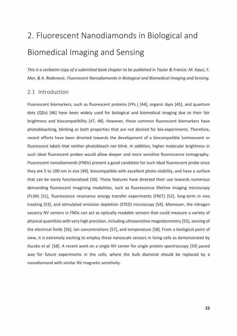
in C3v symmetry by a nitrogen impurity adjacent to a carbon vacancy (shown in Figure 2.2. a).
Figure 2.2: a) A crystal model of the single NV- center (shown in grey) hosted in the diamond crystal lattice having
a substitutional nitrogen (shown in blue) adjacent to a carbon vacancy. Image taken from [61]. b) Energy diagram
of the ground state 3A, excited state 3E, and metastable singlet state 1A represented for NV. Image taken from
[61]. c) High-resolution TEM image of a 5 nm large nanodiamond revealing diamond (111) crystal planes. Scale
bar: 2 nm. Reprinted with permission from [62]. d) Fluorescence time traces for a single 100-nm FND (green), a
single 35-nm FND (red), and a single Alexa Fluor 546 dye (blue). To allow long-term observation, dye molecule
are attached to a single dsDNA molecule, while FNDs were adhered to the glass coverslip. In the 300s time
window, the fluorescence signal was stable with no observation of blinking or photo-bleaching for both sizes of
FNDs. Reprinted with permission from [63].
These defects might occur in nature under high pressure and temperature conditions that occur in
the protoplanetary disks of certain types of stars [64, 65] and also isolated and identified in the
meteorites [66]. Similarly in artificial FNDs, NV centers are produced either under high pressure and

25
temperature or can be generated through electron and ion irradiations [67]. The irradiation
damages in the diamond lattice can be annealed to diffuse the vacancies to the implanted nitrogen
atoms. Recently, defect hosting in a FND as small as 5 nm has been synthesized [62, 68] (shown in
Figure 2.2. c). This opens a gate for nanoscale drug delivery and real time monitoring of various
physical quantities, such as temperature [69], pressure [70], magnetic field, and ionic
concentrations [71] in a cellular environment.
A single NV- defect exhibits two level quantum system and as there is a short lag between the
excitation and subsequent decay, it emits a photon at a time, which enables single photon
applications. It has non-photo bleaching non-blinking stable fluorescence characteristics with a
quantum yield close to unity at room temperature. In terms of bio-imaging, these unique properties
are extremely useful. For example, broad fluorescence emission conveniently centered around 700
nm, guarantees negligible interference with cellular autofluorescence (see Table 2.1). The
fluorescence signal of these defects, hosted in NDs larger than 5 nm, is extremely stable devoid of
blinking and photobleaching [55, 72]. Furthermore, it has been demonstrated that diamond
nanocrystals hosting NV- defects are biologically inert and do not induce cytotoxicity and apoptosis
in most tested cell lines [50, 73]. Yet, numerous functionalization protocols took advantage of either
hydrophilic-oxygen terminated diamond surface or hydrogen terminated surface resulting in the
applications where FNDs were coupled to proteins [74] and DNA molecules [75]. Recently, FNDs
functionalization has been simplified exploiting silica encapsulation allowing better colloidal stability
[76]. All the above-mentioned properties make FNDs a promising candidate for the next generation
of biomarkers. In order to put into context the performance of this newly emerged biomarker, Table
2.1. lists literature reported values of fluorescent properties for single NV--, quantum dot, typical
organic dye, EGFP protein, and cellular proteins that give rise to auto-fluorescence. It is evident that
single NV- center will outperform both quantum dots and EPGF protein cluster while cellular
autofluorescence is an order of magnitude lower.

26
Property NV-- defect in nanodiamond
Quantum dot [77]
Organic dye [77]
EGFP Auto-fluorescence of protein clusters
Size >4 nm [62, 78] 3-10 nm <1 nm ~3 nm >3 nm
Quantum yield 0.7-0.8 0.1-0.8 0.5-1 0.6 0.26 [79]
Lifetime 25 ns 10-100 ns 1-10 ns 1-4 ns [80] NA
Molecular brightness
500-100 kcps 50-200 kcps 10-150 [81] 25 kcps [82] 2.1 kcps [82]
Bleaching No No Yes Yes Yes
Blinking No Yes Yes Yes Yes
Emission
spectrum
680-800 nm IR-UV
selected by
size
IR-UV
selected by
type
500-520 nm 250-650nm
Toxicity Low From low to high
Dye dependent
None None
Thermal stability
High High Low Low Low
Table 2.1: Comparison of fluorescent properties for single NV-, quantum dot, typical organic dye, EGFP protein, and
cellular proteins that give rise to cellular auto-fluorescence.
In addition to their use in imaging, NV- defects hosted in FNDs are extensively employed in quantum
computing due to their long spin coherence time [83], and optically addressable spin states [83]. At
room temperature, NV center has a sharp ZPL, arising by zero-zero vibronic transitions, that is well
resolved from the phonon side bands (PSBs), arising by phonon assisted transitions. The
indistinguishable photons in the ZPL make it an outstanding emitter for quantum optics [84, 85].
The basic motivation behind NV- centers as building block of the hardware for quantum computing
is its high level control properties on a solid-state platform. Owing to its atom-like structure, NV-
defects are a promising alternative to trapped ions that are isolated from environmental couplings
and hence offer high precision measurements [86]. While the isolation approach imposes special
requirements (e.g. high vacuum, low temperature) on the environment and complicates integration
stage and scaling up of the technology, the NV- defects hosted in FNDs are capable of operating
under ambient conditions. As single NV- center has a nuclear spin with long coherence time, which

27
can be used as quantum register, and an electron spin, which can be used as a control or detection
unit of nuclear spins, it has been intensely studied for the realization of quantum processors.
NV- centers in FNDs have two unpaired electrons forming electron spin triplets, S=1, in the ground
and excited states. Optic excitation operates as a pump for ms=0 sublevel of the ground state, 3A.
Given that ms=0 and degenerate sublevels ms=±1 are separated by zero field splitting parameter D,
a resonant microwave signal will excite optically populated ms=0 state to the ms=±1 states at this
frequency (as shown in Figure 2.2.b). As ms=±1 states have higher probability of going intersystem
crossing (ISC), which leads to a decrease in the fluorescence, this mechanism serves as basis of
optically detected magnetic resonance (ODMR). The ODMR spectrum of NV center is a powerful
tool used in nanoscale sensing as it reflects local physical perturbations influencing the state
transitions. It has been shown that the splitting parameter D is temperature [58] and pressure [70]
dependent and that single NV center can be used as a sensitive nanoscale sensor (see Table 2.2).
In the presence of a static magnetic field aligned to NV center quantization axis, field ms=±1
degeneracy shifts by , where is NV gyromagnetic ratio. When the field is not aligned,
multiple centers in a single FND provide four resonance shifts in the ODMR spectrum with each for
one crystallographic axis projection. Using this property, one can resolve vector magnetic field by a
reference magnetic field fixed in orientation.
Physical quantities can also be resolved via pulsed ODMR spectroscopy, as single NV center can form
an effective two-level quantum system. In Ramsey pulse sequence scheme, the phase acquired in
the free precession time is proportional to the external magnetic field. Therefore, the spin
dependent PL of NV center can be used for DC magnetometry [87]. Moreover, a spin echo pulse
sequence synchronized to an AC field behaves phase additive on each half of the sequence, which
can be used for AC magnetometery [88]. In such pulsed experiments, as the optic and microwave
excitations are not performed simultaneously, the microwave excitation tuned down will reduce the
power broadening and the optic excitation tuned up will increase the collected photons resulting in
an enhancement in sensitivity compared to continuous wave excitation experiments.
High-spatial-resolution magnetic field detection cannot be performed in cell-like environments with
methodologies such as SQUIDs [89], the Hall effect in semiconductors [90], atomic vapor based
magnetometry [91], as well as magnetic resonance force microscopy [92]. Measurement of weak
magnetic fields in biological samples with nanometer spatial resolution is thus an important
problem to study. The possibility to detect such weak magnetic fields has become possible through

28
taking advantage of the above mentioned quantum properties of NV centers. As a sensor, NV
centers are better suited to probe magnetic fields compared to electric fields, due to its moderate
sensitivity to the applied electric field compared to quantum dots [56] (see Table 2.2). NV centers
embedded in single FNDs make the measurement of magnetic fields possible with hundreds of nT
Hz-1/2 sensitivity due to the fact that the applied static or oscillating magnetic field causes the relative
energy shift between two Zeeman sublevels. While, in the case of electric field sensing, the electric
inaction caused by the Stark effect and spin orbit coupling is much weaker and reflected in lower
sensitivity.
Researchers have shown the possibility to sensitively detect individual charges in 3D by the rotation
of a magnetic bias field [56]. This methodology is designed around a quantum-metrology technique
based on a single NV defect center spin in FND, which could reach a sensitivity of 202 V cm-1 Hz-1/2.
This is equivalent to a single elementary charge placed at a distance of ~ 150 nm from the FND
particle probe and sensing NV spin within one second averaging was required. In addition, 100-s
averaging was needed to sense a single electron charge from a distance of 35 nm with a signal-to-
noise ratio of more than 1000. Similarly to magnetic field detection [87], the sensitivity on electric
fields measurements is much better when performed with the field-induced phase accumulation
method [56]. Increasing the evolution time, , from 8 to 80 μs allows a more precise determination
of minimally detected electrical fields as small as 7 V cm-1.
Temperature sensing at nanoscale and with high sensitivity is also possible using single defects in
FND. The spatial resolution is related to the size of the FND, as in NSOM, whereas the sensitivity
depends on the NV concentration [69]. The temperature noise floor that can be reached
corresponds to 5 mK Hz-1/2 for single defects in bulk sensors. In contrast, the temperature noise floor
is 130 mK Hz-1/2 with a precision down to 1 mK for nanocrystal sizes [93]. In consequence,
temperature can be probed over length scales of a few tens of nanometers. The unique possibility
to combine such accuracy and position resolution with the high photostability of FNDs should enable
detection of heat produced by chemical reactions taking place among single molecules. In the
absence of an external magnetic field, the temperature shifts the ground state electron spin
polarization, mS = 0 with respect to the sublevels mS = ±1. Experimentally, this shift, referred to as
axial ZFS, was found to vary significantly as of function of temperature [69]. To sense the
temperature, one optically measures either the parameter D (~ 2.87 GHz) with the ODMR technique
[69], which corresponds to the ZFS, or the ground state spin coherence time (~ 1 ms) [58, 94]. The
principle of the latest method is to detect the NV fluorescence modulated with cos(2 ∆D ), that is,

29
a D-Ramsey oscillation with frequency ∆D. Fluorescence as a function of evolution time provides an
increasing phase accumulation, , and thereby improving the temperature uncertainty [58].
Increasing from 50 to 250 μs makes it possible to identify temperature variations as small as 1.8
mK in an ultrapure bulk diamond sample [58].
Property Typical Sensitivity Reference(s)
Pressure 6.8 bar √Hz
Via zero field splitting parameter D
[70]
Temperature 0.13K√Hz Via zero field splitting
parameter D [69]
Magnetic field 0.36 T/√Hz Zeeman effect [55, 88, 95]
Electric field (εxy=280 εz 5.8) V cm-1/√Hz
Stark effect and spin-orbit coupling [56, 96]
Orientation 0.1°√Hz Via zero field splitting parameter D
Table 2.2: NV based sensor typical sensitivities adapted from [97].
2.3 Nanoscale Imaging of Biological Systems with NV-centers Hosted in
Nanodiamonds
Due to their high photostability and biocompatibility, FNDs are well-suited far- and near-field probes
for imaging purposes of intracellular environments with resolution below the diffraction limit. The
first reported use of FNDs as biological markers for diffraction limited imaging dates back to 2005
when a team lead by Huan-Cheng Chang demonstrated that FNDs are spontaneously internalized in
HeLa cells and display no cytotoxicity [50] (see Figure 2.3. a). Besides imaging, single particle
tracking (SPT) techniques are instrumental when studying the bio-molecular activity occurring at
the intracellular level. Shortly after, their application in fluorescence imaging, excellent
photostability of FNDs has been exploited for long-term three-dimensional tracking of single 35 nm
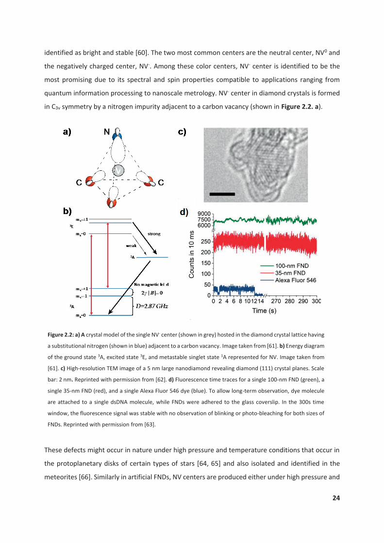
large FNDs in a living cell [49] (see Figure 2.3 b).
30
Figure 2.3: a) The cross-sectional confocal fluorescence images of a single 293T human kidney cell after FND uptake.
Inset shows cell viability test demonstrating low cytotoxicity of FNDs. Reprinted with permission from [50]. b) Three-
dimensional tracking of a single FND in the cytoplasm of a living cell. Merged bright-field image of the HeLa cell with
the epifluorescence image of the single FNDs and FNDs agglomerates. c) 3D trajectory of the selected single FND
particle (shown in b)). Single FND is followed for about 200 s as it diffuses through the cytoplasm. b) and c) adapted
with permission from [49].
Chang et al. could track single FND for periods longer than 200 s. Since then the use of FNDs as
biomarkers and as fluorescent probes for long-term tracking has exploded and now it is not only
limited to the cells, but also includes organs and model organisms (including C. elegans [98],
Drosophila [99], Mice [100], and Zebrafish [101]), which allows to study a wide range of biomedical
problems, such as organ development [51], embryogenesis [99], stem cell proliferation [51],
neuronal survival and morphogenesis [102], and cancer cell identification [103]. In addition, FNDs
as biomarkers have opened the door to novel imaging and SPT modalities that are not accessible to
conventional fluorescence microscopy, including orientation tracking over long periods, with
resolution in the millisecond timescale of intracellular events [104]. In biomedical imaging, NDs are
used as contrast agents in magnetic resonance imaging (MRI) [105].
2.4 Super-resolution Microscopy with Fluorescent Nanodiamonds
The past decade has been marked with the rapid progress in super-resolution microscopy. Methods
based on localization and tracking of single-particle light emitters are required for applications
ranging from high-resolution optical microscopy and bio-sensing to single molecule detection [106].
Even though fluorescent proteins and organic dyes are standard probes in the domain of super-
resolution localization microscopy, nanosized photoluminescent probes with efficient linear and
nonlinear optical response, including FNDs [107, 108], ferroelectric perovskites [109-112], and
upconverters [113] are attracting researcher’s attention. Although all these kinds of particle-probes
a) b) c)

31
are by its virtue highly photostable and low-power laser excitation, with the possibility to obtain
FNDs smaller than fluorescent proteins [66] makes them the most suited labelling candidates to
circumvent the diffraction resolution barrier down to a few nanometers. Near-field scanning optical
microscopy (NSOM) of soft biological structures and the detection of molecular interactions became
possible after the advent of AFM and force spectroscopy techniques. Essentially, NSOM presents
the first nanoscopy imaging technique and it exploits the evanescent field produced by a
subwavelength aperture. In 1928, Edward H. Synge (1890-1957) proposed the original idea for
NSOM; however, it took more than 50 years to experimentally realize this idea requiring a
technological progress development of lasers, microfabrication of subwavelength apertures,
precision positioners, single-photon detectors, and computers [114-116].
Figure 2.4: a) First NSOM scan
taken with the fluorescence
nanodiamond attached to the tip.
The scan is taken in a constant-gap
mode across a section of a gold
mask. Adapted with permission
from [108]. b) Luminescence image
of a single FND. The image is
recorded at an excitation optical
power of 100μW measured at the
tip apex. Corresponding optical
cross-section. Adapted with
permission from [117].
Interestingly, the resolution in NSOM, which allows for simultaneous high-resolution measurements
of topology and fluorescence, is not limited by light diffraction, but by the size of the scanning probe,
which is composed by a tapered optical fiber having a diameter of ~ 50 nm. Inspired by scanning
optical microscopy, it has been reported that a single FND can be attached to a NSOM tip and used
as a local light source [108]. Excitation of the FND crystal at the end of the tip was performed using
an illumination light waveguided through the fiber holding it. The NSOM images taken with the FND
crystals as a light source of a gold mask in fluorescence mode showed, however, a resolution of only
300 nm shown in Figure 2.4. a. To further increase the resolution, it was proposed to implement
b)a)

32
tips with smaller crystals with a single colour center [108]. Significant improvement in resolution
has been achieved by using much smaller FNDs of 25 nm. Figure 2.4 b, demonstrates that NSOM
can detect nonbleaching luminescence signal from an individual FND hosting a single NV color
center [117]. Here, reported FND was smaller than 25nm in diameter. Another possibility to
overcome the diffraction limit is to exploit the effect of stimulated emission discovered by A.
Einstein [118], and subsequently demonstrated experimentally by S. Hell [119, 120].
In brief, STED microscopy is a far-field approach that takes advantage of the limitations of matter to
be imaged in order to reconstruct a super-resolution image. Stimulated emission is a physical
process where an excited atomic electron, or an excited molecular state, may drop to a lower energy
level transferring its energy to an electromagnetic wave of a certain wavelength. In addition to the
excitation laser, a second-laser, referred to as STED laser, cancels fluorescence of the emitter
located outside the center of excitation.
Technically, the doughnut-shape de-excitation STED laser is realized with a phase modulator. STED
microscopy was used to image NV centers with nanoscale resolution and using focused laser light
[107]. Only the NV centers hosted in FND that are located in the subdiffraction-sized area around
the doughnut, where the STED beam intensity is lower than the threshold of the excited state
depletion by stimulated emission, are not turned off and therefore still allowed to emit and to be
identified among multiple centers present in 50-100 nm large FND (see Figure 2.5).
To achieve such performances, the intensity of the STED laser, ISTED, has to be in the order of GW
cm-2 pointing that only robust markers can be used. In case of highly photostable FNDs, application
of ISTED = 3.7 GW cm-2 was needed to reduce the focal spot, i.e. FWHM, from 223 nm in diameter
down to 8 nm [107] as shown in Figure 2.5 a-c. Further increasing ISTED up to 8.6 GW cm-2,
compresses the FWHM to values as small as 5.8 nm in 1D, which is still predicted by the theoretical
inverse square-root law [121]. This value is 133 times smaller than the used wavelength for imaging
the colour centers in single FNDs and represents a new regime in optical-based microscopy.
Recently, up to 5 single NV cementers have been resolved from the single FND using super-resolving
STED microscopy [122] Figure 2.5 d-e.

33
Figure 2.5: a) Conventional confocal microscopy image, which displays a featureless image, while in b) the super-
resolving STED microscopy image reveals individual luminescent NV centers inside the diamond crystal. c)
Corresponding vertically binned STED image profile showing one NV center. Figures a) b) and c) were adapted with
permission from [107]. d) Subdiffraction resolution STED image of single FND hosting 5 NV centers and e)
corresponding vertically binned STED image profile. Figures d) and e) were reprinted with permission from [122].
Manipulation of spin degrees of freedom using conventional far-field optical microscopy techniques
is limited by diffraction. In principle, one cannot resolve spins by less than 250 nm. In contrast, the
spin- reversible saturable optical linear fluorescence transitions (RESOLFT) microscopy, developed
specifically for far-field imaging and manipulation of individual NV electronic spins in FND, revealed
a nanoscale resolution [123].
a) b) c)
d) e)

34
Figure 2.6: a) Experimental sequence of spin-RESOLFT. NV spins are first optically pumped to ms=0 with a
Gaussian beam at 532 nm followed by microwave manipulation. Application of a 532 nm doughnut beam
repolarizes the outer ring to ms=0, which allow the spin state of the central dark region to be independently
read-out. b) In the confocal (image left), it is not possible to multiple NV- centres, whereas 2D spin imaging
using spin-RESOLFT (image right) clearly resolves two NV centres separated by ~150 nm. Reprinted with
permission from [123].
The basic idea in the spin-RESOLFT approach for spin detection and control with subdiffraction
resolution is shown in Figure 2.6 a: (i) to polarize by optical pumping a NV center, (ii) coherently
manipulate the NV center with resonant microwave and (iii) detect its spin-state-dependent
fluorescence [123]. To improve the spatial resolution, the sample is illuminated with a doughnut-
shaped laser beam, as in STED microscopy, just before reading the spin state. In consequence, spins
that are not in the center of the doughnut contribute differently to the fluorescence signal
compared to spins located at a few nanometers from the center of the beam. Using the spin-
RESOLFT technique applied to an NV center in the diamond, it is possible to optically image a single
spin with a resolution down to 38 nm employing only 2-mW total doughnut beam power focused to
a diffraction-limited spot of 0.07 μm2 [123]. The resulting intensity corresponds to ~ 3 MW cm-2, and
can be further reduced by a factor of 20 while keeping a similar resolution by increasing the duration
of the doughnut pulse, tD, from 12.5 to 100 μs [123]. Compared to STED, the spin-RESOLFT
a)
b)

35
microscopy technique needs 4 orders of magnitude less power for comparable resolution [107]. It
is also interesting to note that the length of tD is limited by the spin-state relaxation time (> 100 ms)
and the electronic excited-state lifetime (~ 10 ns) [123].
On one hand, we have deterministic super-resolution imaging techniques, such as STED and spin-
RESOLFT, which are capable of resolving NV centers down to 5.8 nm and 38 nm, respectively [107,
123]. However, these approaches require either a high power density for the doughnut-shaped
depletion beam (~ 1GW cm-2) [107], or due to the serial scanning measurement results in a slow
frame rate [123], leads to the problematic imaging of dynamic processes in living cells.
Stochastic super-resolution imaging techniques, such as PALM [124, 125] and STORM [126], which
are based on the localization of sequentially activated photo-switchable fluorophores, are better
suited for fast image acquisition. However, they are affected, among others, by the precise
localization of stochastic switching events and the compromise between bleaching and imaging
rate. In consequence, the search of fast and noninvasive non-scanning imaging techniques with sub-
diffraction resolution and accuracy continue. In contrast to PALM and STORM, the wide-field super-
resolution microscopy using spin-dependent fluorescence in nanodiamonds, referred to as
deterministic emitter switch microscopy (DESM), demonstrated the capability to image a 35 x 35
μm2 surface composed by 100 NV centers in FNDs with a localization precision between 12 and 46
nm, and employing only 90 s [127]. In DESM, the principle is to exploit the dependence of the
fluorescence intensity of the NV centers as a function of the spin orientation. In this context, the
ODMR technique allows to measure the spin resonance frequencies of all centers within a
diffraction-limited spot. If the centers do not overlap, one can distinguish them by microwave
excitation in a deterministic way. In consequence, this methodology works properly while FNDs are
arbitrarily oriented leading to multiple spin transitions. The basic procedure in DESM to achieve a
sub-diffraction resolution is to resonantly drive only one ground-state spin transition at a time [127].
Up to now, the world record in far-field based super-resolution optical microscopy, i.e. 8 nm in 2D
and 5.8 nm 1D, is held by NV centers embedded in single FNDs [107].

36
2.5 Nanoscale Sensing of Biological Systems with NV centers Hosted in
Nanodiamonds
As introduced in the section related to sensing properties of NV centers hosted in FNDs, various
physical properties can be detected with high accuracy. Here, we detail the two most prominent
examples related to biological systems.
So far, temperature measurements of biological environments at nanoscale resolution presented a
grand challenge in metrology. However, using the NV centers hosted in FNDs, according to Kucsko
et al., demonstrate nanoscale temperature probing of the interior of single human embryonic
fibroblasts [58]. By inserting FNDs into single living cells, the FNDs were then irradiated with
microwaves in order to modulate the electron occupancy of spin states. To determine the changes
in the ground-state energy gap, authors used wide field fluorescence measurements that allowed
to probe the temperature variations (the microwave frequency that corresponds to the energy
difference between spin states) for several FNDs. The temperature inside the living cell has been
also modulated by irradiating and heating the gold nanoparticles in the cell (see Figure 2.7 a. and
Figure 2.7 b). Although most of the exciting applications of FNDs are related to fluorescence-based
microscopy, especially in biology, where room-temperature functionality and chemistry are crucial
parameters, another interesting sensing area is 3D MRI with NV centers hosted in diamonds.
In principle, a 1 nm resolution of single electron spins in a solid has been demonstrated [95], while
a resolution of 400 nm has been achieved for living cells [128]. In contrast, in medical facilities and
for biological tissues, the resolution for conventional MRI apparatus is about 1 mm, which
demonstrates the huge potential for 3D MRI with NV centers hosted in diamonds. The most
prominent example of the magnetic imaging on biological samples has been demonstrated using
the magnetic field imaging array consisting of a nanoscale layer of nitrogen–vacancy color centers
implanted on the surface of a diamond chip. Le Sage et al. have succeeded to localize magnetic
nanoparticles (magnetosomes) produced in the magnetotactic bacteria (MTB) with sub-cellular
spatial resolution (see Figure 2.7 c. and Figure 2.7 d.) [128]. Authors suggest that their method can
be used to identify potential vertebrate magnetoreceptor cells [129], which should have a magnetic
moment that is comparable to or larger than one found in MTBs.

37
Figure 2.7: a) Confocal scan of a single living cell obtained using a laser excitation set to 532 nm, with a collection
at wavelengths greater than 638 nm, which ensures collection of PL signal mostly from FNDs. The cross mark
indicates the position of the gold nanoparticle used for heating, and the circles represent the location of the FNDs
(NV1 and NV2) used for thermometry. Color bars indicate the fluorescence in counts per seconds. b) Measured
temperature change at the positions of NV1 and NV2 relative to the incident laser power were applied to the gold
nanoparticle. (a,b) Reprinted with permission from [58]. c). Wide-field optical image of dried MTB on a diamond
chip. Inset shows a typical transmission electron microscope (TEM) image of a single MTB. Dark spots inside MTB
are magnetite nanoparticles. d) Stray field distribution recorded with a wide-field NV magnetometer –imaged
region corresponds to the one shown in c). (c,d) Reprinted with permission from [128].
2.6 Manipulation Techniques
In order to apply the full FND sensing in nanoscience and biology, the sensing probe in the form of
the single FND, has to be positioned and manipulated with high accuracy over the sample. Several
exiting techniques, such as scanning probe techniques, optical tweezers, and ABEL trap have
reached required precision.
2.6.1 Scanning Probe
Due to its electronic and optic properties, a single NV center embedded in a FND can be attached to
a probe tip, i.e. AFM, for atomic scale resolution in imaging, as shown in Figure 2.8. The idea is to
bring the scanning probe close to the substrate surface and detect the local fields emanating from
a) b)
c) d)

38
the sample through the change in the spin dynamics. The spin dependent PL of NV center can be
collected via far field optics, whereas optic and microwave excitations are realized in ensemble level.
Alternatively, a fiber optic waveguide, serving as scanning probe that can be functionalized such
that it delivers microwave signal through an integrated transmission line, performs optic excitation
and collects the fluorescence simultaneously [130, 131]. Recently, an engineered NV center hosted
in a scanning nanopillar waveguide with long coherence time (~75μs) and collection efficiency was
shown to be a sensitive robust magnetometer imaging magnetic structures as small as 25 nm (see
Figure 2.8 d.) [132].
Figure 2.8: Scanning probe based FND manipulation techniques a) In the near-field scanning optical microscopy
(NSOM/SNOM) FND has to be first picked by an optical fiber and then is scanned over the magnetic
nanostructure. Reprinted with permission from [130]. b) Depicts basic principle of all scanning magnetometery
techniques. In AFM, a sharp tip with a nitrogen vacancy center at the tip maps out the three-dimensional
magnetic field vector above a magnetic nanostructure. Reprinted with permission from [133]. Several methods
have been developed in order to position/fabricate the FND on the cantilever tip. c) FND can be picked up from
the surface and attached to the cantilever tip. Reprinted with permission from [133]. d) Alternatively, diamond
nanopillar probe with a single NV center in its tip can be fabricated from of a single crystalline as shown in SEM
image Reprinted with permission from [132] .
Similar to the conventional MRI technique, the scanning probe tip can also be employed for the
generation of a magnetic field gradient on NV centers [55]. This modality basically aims to detect
the resonance ring of each NV center that appears by scanning the corresponding magnetic field
under a fixed microwave excitation. Given the probe position, the gradient profile is known, and the
NV centers can be localized with the ultimate resolution limited by the resonant ring width.
Microwavesfor EPR
Substrate
Single spinin diamond tip
A surface electron spin
CantileverTo opticsa)
5μm
b)
d)
c)

39
Recently, a spatial resolution of 9 nm has been demonstrated for proximal NV centers in clustered
form. In all scanning configurations the optic data acquired by NV center can be easily correlated to
topography mapping achieved with the probe tip for further enhancement in the imaging.
2.6.2 Optical Tweezers
Although the integration of single NV center to a scanning probe tip remarkably improved
resolution, this approach has some drawbacks regarding experimental realization and operating
environment. Firstly, to sense the local fields with high spatial resolution, the NV center should be
placed close to the probe tip that requires nanoscale positioning and expensive fabrication process.
Consequently, a significant effort has been put into the engineering NV defects in the diamond.
Recently, stable NV centers as close as 2 nm to the diamond surface have been formed without
degrading spin coherence time [134]. Yet, this limit is far beyond realization for the FND integrated
to a scanning probe. Also, the probe tip may perturb the environment or the intrinsic characteristics
of NV center. Moreover, as this approach is limited by operating environment of the probe tip, it is
not a practical solution for closed microfluidics and bio-applications. Recently, optic-based trapping
has been demonstrated as a nanoscale positioning tool for FND hosting NV centers [135] see Figure
2.9. a. This technique uses a piezoelectric stage performing 3D scanning of the sample with respect
to the focused infrared beam where multiple FNDs are trapped through the radiation pressure. A
second green laser optically excites the NV centers in FNDs, while the microwave signal is applied
through a nearby antenna. Although the large ensembles of NV centers are randomly oriented in
such trap environment, it is shown that the local DC magnetic field sensing is possible. Moreover, a
recent work using counter propagating dual beam technique has achieved the trapping at single
particle level [136] Figure 2.9. b. It is also shown that the orientation of the polarized beam on
asymmetric nanodiamond can provide the control over the angle between the optic axis and the NV
quantization axis with high accuracy. This progress facilitates three-dimensional directional
magnetometer in solution.

40
Figure 2.9: Two configurations base on 3D optical trapping optical trapping of FNDs that allow for manipulation
of a single electron spin. a) Single beam optical tweezers, photoexcitation, and luminescence detection are
integrated on the same setup using a High NA objective. The magnetic field is applied externally, along the axis
of the objective. Reprinted with permission from [135]. b) The dual beam optical tweezers permits accurate
control over the FNDs orientation. Reprinted with permission from [136].
2.6.3 ABEL Trap
Despite the fact that laser based trap is an outstanding manipulation tool for aqueous
environments, it is not functional for FNDs of smaller sizes. Given that the force generated in optic
tweezers is proportional to the volume of the trapped object, particles smaller than 100 nm requires
high optic powers (~150 mW) [137]. This is not desirable in biological environments as it may affect
the properties of the trapped particle, as well as the medium. Moreover, as the force arises through
a second order interaction, the applied field must first polarize the object, and then generate the
force between the induced dipole and a gradient in the field. The ABEL trap is a novel approach to
overcome size limitations in a solution phase trapping.
It combines laser guided single particle tracking with a real time feedback, which cancels the
Brownian motion. Unlike optic tweezers, the trap force is not optic based, but electrokinetic which
scales linearly with the particle radius. Recently, single dye molecule of sub-nanometer size has been
successfully trapped by a very low optic excitation power used in the particle tracking [138]. As the
trajectories of diffusing particles are not correlated; thus, only one is exposed to the correct
feedback, exactly one particle is trapped with this method. Moreover, all surrounding particles
around the trap point are subjected to the same feedback, therefore applied electrokinetic force on
a) b)

41
native environment is not perturbative see Figure 2.10. This also avoids any potential clustering or
agglomeration that might occur in optic tweezers for dense dispersions.
Figure 2.10: a) Schematic of ABEL trap PDMS microfluidic cell with RF circuit integrated on the glass coverslip. Inset
show a zoom in the trapping area and it indicates the relative location of FND in respect to the area with the enhanced
homogeneous magnetic flux density. b) Typical ODMR spectra of NV defects in ABEL trapped FND. b) Optically detected
ESR spectra of an ABEL trapped single FND under presence of the weak and strong static magnetic field. Image taken
from [61].
Provided that these advantages ABEL trap is an outstanding tool for FND manipulation and
positioning. Indeed, more recently this approach has been validated with electron spin resonance
experiments on 30 nm sized FND containing NV centers [61]. Although the particle has rotationally
free behavior, the detection of static magnetic fields through the ODMR spectra has been
demonstrated [61].
Moreover, a work by Maclaurin et al. [139] on single diffusing diamond nanocrystal shows the
capability of the ABEL trap approach for sensing also the fluctuating and oscillating magnetic fields.
As well as being a sensitive magnetometer, ABEL trap is compatible to other NV center based
a)
microwavecircuit
ABEL trap
glass coverslip
PDMS
Vx+ Vy+
Vy- Vx-
1.00
0.98
0.96
0.94
0.92
0.90
0.88
0.86Nor
mal
ized
Inte
nsity
2.902.892.882.872.862.852.84
Frequency (GHz)
b)
0.96
0.94
0.90
1.00
0.98
0.92
Nor
mal
ized
Inte
nsity
3.002.9502.9002.8502.8002.750
Frequency (GHz)
strong magnetic field
weak magnetic field
c)
42
detection schemes, such as thermometry and ion concentration measurements. With the advances
in fabrication of stable FNDs, this technique will provide a new valley for three-dimensional high
resolution imaging and sensing in fluidics and physiological environment.
2.7 Conclusion
With this chapter we attempted to give a short overview of the emerging new probes in the form
of FNDs. We focused on their use in nanoscale imaging of biological samples and biological relevant
sensing application, such as single cell thermometry and magnetometery. In relation to the sensing
we have also reviewed current nanoscale manipulation techniques that would allow in the future
positioning of these ultrasensitive sensors within a single living cell.

43
3. Single Fluorescent Nanodiamond in a Three-
Dimensional ABEL Trap
This is a verbatim copy of an article that has been published in a peer reviewed journal: M. Kayci &
A. Radenovic . Single fluorescent nanodiamond in a three dimensional ABEL trap. Scientific Reports
5-16669 (2015)
3.1 Abstract
Three-dimensional single particle trapping and manipulation is an outstanding challenge in various
fields ranging from basic physics to life sciences. By monitoring the response of a trapped particle
to a designed environment, one can extract its characteristics. In addition, quantum dynamics of a
spatially scanned well-known particle can provide environmental information. Precise tracking and
positioning of such a particle in an aqueous environment is a crucial task for achieving nanoscale
resolution. Here we experimentally demonstrate three-dimensional ABEL trap operating at a high
frequency by employing a hybrid approach in particle tracking. The particle location in the
transverse plane is detected via a scanning laser beam, while the axial position is determined by
defocused imaging. The scanning of the trapped particle is accomplished through a nanopositioning
stage integrated to the trap platform.
3.2 Introduction
Single particle trapping and manipulation can provide inner dynamics of single molecules that are
not resolvable in ensemble level averaging measurements. Optical trap is one of the most powerful
techniques that has been used for nanoscale positioning in biophysics and quantum optics.
Recently, it has also been proposed as a three-dimensional scanning tool for nitrogen vacancy
embedded single nanocrystal employed in quantum sensing [140]. However, this technique is not
practical for particles smaller in size since the optic forces required for stable 3D trapping are
proportional to the particle’s volume. High optic powers on such particles may introduce heating
that could perturb the biological environment [141]. Moreover, as any particles near the beam focus
are subjected to the trapping forces, it is not selective. Therefore, single particle level trapping
requires extremely low concentration, which is not the case for very crowded physiological
environments. Instead, electromagnetic tweezers [142] can provide single particle selectivity since

44
they operate by active feedback control. However, the trapping is limited to magnetic beads and
high driving currents on electromagnets could result in a substantial heating, which in turn requires
an active cooling system. Less common, modalities such as dielectrophoresis [143], acoustophoresis
[144], and Paul trapping [145] have also been used in single particle experiments, but unfortunately,
all these techniques have constraints either related to the trapping environment or trapped particle
characteristics.
ABEL trap is a promising technique that can overcome size limitations, as well as the environmental
issues. It combines a very fast detection scheme with a real time feedback, which compensates the
Brownian motion. Unlike optical or magnetic tweezers, the electrokinetic forces applied in ABEL trap
scale linearly with the particle’s radius. A single dye molecule of sub-nanometer size trapping has
been achieved with a very low optical excitation used in the position tracking [138]. Given that the
Brownian trajectories of multiple particles in the trap area are uncorrelated, only one is subjected
to the correct feedback, hence exactly one is trapped during this process. Also, as all particles are
exposed to the same feedback, the electrokinetic force on the environment is non-perturbative. The
instant feedback does not generate a potential well in the trap area, but a uniform field directing
the particle. This also avoids any clustering and agglomeration that occurs in passive trapping
approaches when working with dense dispersions. Providing both electroosmotic and
electrophoretic actuations, the trapping is not limited by dielectric, magnetic or charge properties
of the particle. Therefore, any traceable particle can be trapped.
Although a two dimensional ABEL trap can provide precise measurements without physical
perturbations like surface tethering [146] or excessive heating [141], the confinement in axial
dimension by the geometry of trapping cavity may introduce undesired interactions. As the cavity
depth used for confinement is very small and nanoscale particles have a very high diffusion
coefficient, during a trapping experiment, such particles will have a very high surface collision rate.
For instance, Rhodamine B in a cavity of 800 nm depth collides to the wall with 87 kHz frequency
[147]. This interference may induce fluorescence quenching or absorption of the particle limiting
the trap period and measurement precision. Improvement on microfluidics material and
modification of the surface chemistry [148] has been proposed to remove such effects, but it
requires complex fabrication process and is has a high cost [149]. Alternatively, a three-dimensional
ABEL trap can provide collision free manipulation without the engineering of the chemical and the
geometric properties of the cavity. Indeed, a recent work has utilized sets of micro electrodes
patterned on two fused silica layers forming the trap chamber to achieve three-dimensional control
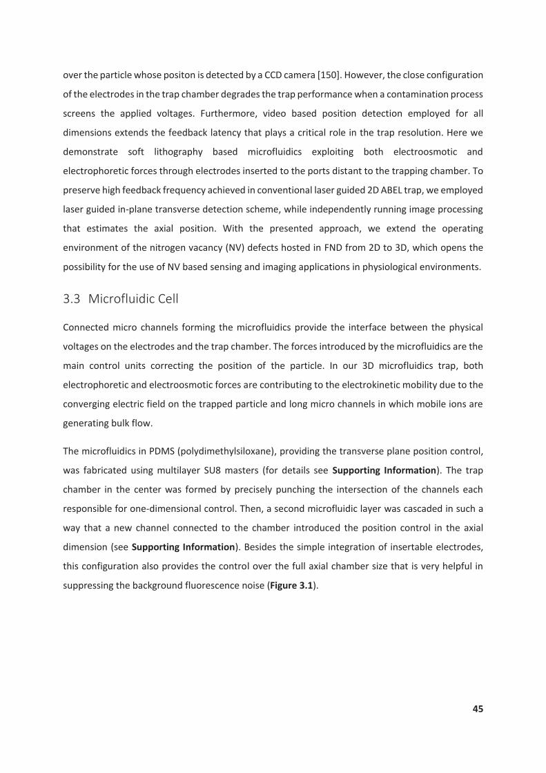
45
over the particle whose positon is detected by a CCD camera [150]. However, the close configuration
of the electrodes in the trap chamber degrades the trap performance when a contamination process
screens the applied voltages. Furthermore, video based position detection employed for all
dimensions extends the feedback latency that plays a critical role in the trap resolution. Here we
demonstrate soft lithography based microfluidics exploiting both electroosmotic and
electrophoretic forces through electrodes inserted to the ports distant to the trapping chamber. To
preserve high feedback frequency achieved in conventional laser guided 2D ABEL trap, we employed
laser guided in-plane transverse detection scheme, while independently running image processing
that estimates the axial position. With the presented approach, we extend the operating
environment of the nitrogen vacancy (NV) defects hosted in FND from 2D to 3D, which opens the
possibility for the use of NV based sensing and imaging applications in physiological environments.
3.3 Microfluidic Cell
Connected micro channels forming the microfluidics provide the interface between the physical
voltages on the electrodes and the trap chamber. The forces introduced by the microfluidics are the
main control units correcting the position of the particle. In our 3D microfluidics trap, both
electrophoretic and electroosmotic forces are contributing to the electrokinetic mobility due to the
converging electric field on the trapped particle and long micro channels in which mobile ions are
generating bulk flow.
The microfluidics in PDMS (polydimethylsiloxane), providing the transverse plane position control,
was fabricated using multilayer SU8 masters (for details see Supporting Information). The trap
chamber in the center was formed by precisely punching the intersection of the channels each
responsible for one-dimensional control. Then, a second microfluidic layer was cascaded in such a
way that a new channel connected to the chamber introduced the position control in the axial
dimension (see Supporting Information). Besides the simple integration of insertable electrodes,
this configuration also provides the control over the full axial chamber size that is very helpful in
suppressing the background fluorescence noise (Figure 3.1).

46
Figure 3.1: The schematics representing the microfluidics geometry. Several outer rings are connecting the ports to
suppress the undesired drifts in the channels. The trap chamber in the center connected to three orthogonal channels
each for one-dimensional control. The feedback voltages on the electrodes (vx, vy, vz) generate the electric field
actuating electrophoresis and electroosmotic forces. The ports are also functioning as inlet and outlet.
3.4 Three-Dimensional Position Tracking
The axial position of the particle was estimated through defocused imaging proposed by Speidel et
al. [151]. The idea is to detect the off-focus distance that is encoded into the intensity pattern in the
image plane. It is shown that for a point-like particle, the size of the outermost ring of the pattern
scales linearly with the axial position. Here, we demonstrated the relation for a wide defocusing
range starting from ≈1 μm above the focus plane (Figure 3.2). Since the random walk of a particle
takes a time-bin of , where is the diffusion coefficient and is the displacement, this
range also defines the maximum feedback latency tolerated in a stable trapping. The optimal target
position is chosen such that it extends the path a particle can travel before it escapes. Once the
position determined the feedback is applied to the corresponding fluidic channel, this compensates
the Brownian motion induced offset.

47
Figure 3.2: a) The size of the outermost ring in the intensity pattern of FND scales linearly with the distance to the
focal plane, z. b) Surface profiles of the grayscale images visualizing the intensity patterns at three different axial
locations. Defocusing stretches the pattern, enlarges the outermost ring size and degrades the image contrast.
While it has sub nanometer detection precision in the axial dimension, this detection scheme does
not provide high spatial resolution in the transverse plane. A large defocus value leads to a spread
in the intensity pattern and a consequential degrade in the image contrast where the location with
the maximum intensity value defines the particle position in the transverse plane. Further, since the
image processing for all dimensions extends the feedback latency, an independently running
detection scheme is preferable for high temporal resolution. Therefore, the detection in the
transverse plane was performed using a real time Kalman filter implemented on a field
programmable gate array (FPGA) device and a rotating laser beam around the target point that
excites the particle with a uniform profile as reported in Kayci et al. [61]. Using an avalanche photo
diode (APD) that feeds the filter on the FPGA device, the positon vector can be precisely determined
upon single photon arrivals. The correcting filter gain, adjusting the feedback strength, is
determined by instant photon count rate and the geometry of the scanning beam (see Supporting
Information). Similar to the axial trapping, to keep the particle at the target location, any shifts in
the transverse plane is cancelled through the in-plane fluidic channels. While for the axial dimension
the feedback rate is mainly limited by image processing speed (≈4 ms) and the camera exposure

48
time (≈10 ms), for the transverse plane it is a function of photon counts on the APD and the
frequency of the scanning laser beam.
3.5 Fluorescent Nanodiamond Trap
To test the performance of the presented three-dimensional ABEL trap, we have used single FND
due to their non-blinking and non-bleaching properties. Due to its optic and spin properties, NV
embedded in a single FND has received a remarkable interest in the last decade. It has been
validated as nanoscale quantum sensor for physical parameters ranging from temperature [58],
pressure [70], and ion concentrations [71] to external electric and magnetic fields. As the particle
presents no bleaching or blinking behavior under ambient conditions, it is well matched to the ABEL
trap manipulation approach. More recently, we showed such FNDs could be used as sensitive
magnetometer in two-dimensional ABEL trap operating in fluidics [61]. After the successful
realization of the hybrid detection scheme in the tracking, here we verified the performance of
technique by three-dimensional trapping and scanning of 25 nm sized single FNDs.
Figure 3.3: a) The estimated positions at which the FND was detected during a trap event. The color bar visualizes the
distance to the target point b) x, y, z displacement histograms during the trap event. The confinement in the transverse
plane (x, y) is better than the axial dimension due to the fast detection scheme.

49
The particle was confined to a nanoscale volume with the displacement values of nm,
nm and nm and thereby setting the trap stiffness (Figure 3.3). As the
uniform excitation is performed by a rotating pencil-like beam with a high depth of focus and the
particle is not photo bleaching or blinking, the emission follows a digital profile when the trap sate
switches (Figure 3.4). Three-dimensional scan of the relative position in the buffer was performed
using a nanopositioning stage. Basically, the displacement of the stage was conceived as
perturbation to be cancelled by the electrokinetic forces as done for the fluctuations driven by the
Brownian motion.
Figure 3.4: The photon counts on the APD when the trap state switches. The profile verifies non-photo bleaching
and non-blinking behavior of the FND. The high contrast in the profile demonstrates the feasibility of sensing and
detection applications exploiting fluorescence decay at magnetic resonance. The intensity of the trapped FND
remains constant in the whole axial range corresponding to 10 um when FND is scanned with the nanopositioning
stage. Current design of microfluidic chip limits the axial range to 10 um.
3.6 Conclusion
Combining computationally independent detection schemes, scanning laser beam guided position
estimation, and defocused imaging, high frequency three-dimensional particle tracking is
demonstrated. The method is verified by ABEL trapping of a single 25 nm sized FND containing NV
defects diffusing in fluidics. The microfluidic cell is fabricated through the soft lithography process
of PDMS. Extension of the ABEL trapping into the third dimension facilitates the scanning of the
trapped particle in the fluidic volume where the temporal and the spatial scanning resolutions are
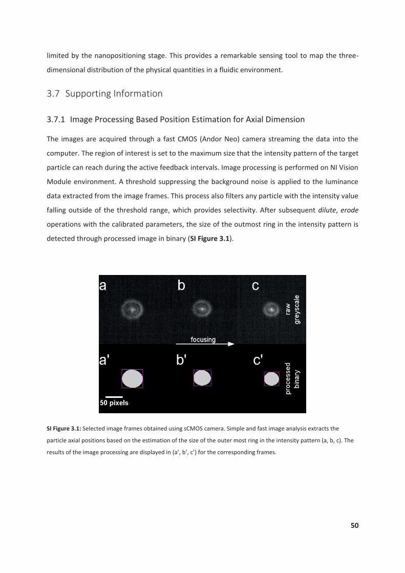
50
limited by the nanopositioning stage. This provides a remarkable sensing tool to map the three-
dimensional distribution of the physical quantities in a fluidic environment.
3.7 Supporting Information
3.7.1 Image Processing Based Position Estimation for Axial Dimension
The images are acquired through a fast CMOS (Andor Neo) camera streaming the data into the
computer. The region of interest is set to the maximum size that the intensity pattern of the target
particle can reach during the active feedback intervals. Image processing is performed on NI Vision
Module environment. A threshold suppressing the background noise is applied to the luminance
data extracted from the image frames. This process also filters any particle with the intensity value
falling outside of the threshold range, which provides selectivity. After subsequent dilute, erode
operations with the calibrated parameters, the size of the outmost ring in the intensity pattern is
detected through processed image in binary (SI Figure 3.1).
SI Figure 3.1: Selected image frames obtained using sCMOS camera. Simple and fast image analysis extracts the
particle axial positions based on the estimation of the size of the outer most ring in the intensity pattern (a, b, c). The
results of the image processing are displayed in (a’, b’, c’) for the corresponding frames.

51
3.7.2 Kalman-Filter Based Position Estimation in the Transverse Plane
In this approach, a pattern is fed into electro optic deflectors scanning the sample plane. Then
through fluorescence photons arrival times (detected by a Single Photon Counting Module SPCM),
the position of the molecule is obtained. As the beam has a finite size, these positions are not precise
and so-called measured positions with a measurement noise. A digital filter, Kalman-filter, is used
to estimate the real positions. A summary of the recursive algorithm is given in section 1.3.3. The
filter is implemented in a NI-FPGA device). Details on the set-up can be found in Kayci et al. [152].
3.7.3 Microfluidic Cell Fabrication
The SU8 master defining the geometry of the transverse plane microfluidics was fabricated in many
layers that the thickness of the channels is minimum around the trap chamber. This facilitates better
electrical contact for the electrodes and higher electrokinetic mobility in the trap chamber. The
microfluidics were formed using PDMS spin coating of the master with a thickness value setting the
depth of the trap chamber. Then, the mold was peeled off and transferred to a clean PDMS base for
punching process (SI Figure 3.2). The location of the trap center was punched as circular cavity of
300 μm in size to connect the fluidic channel in a second layer. Similarly, the fluidic channel in the
second layer was made and plasma bonded to the first layer such that the end port of the channel
enclosed the trap chamber (SI Figure 3.3). This connection couples the control into the axial
dimension. The alignment was performed precisely under a microscope. Then, the cell was punched
to introduce the integration ports for electrodes. These ports also serve as inlet and outlet for the
sample. Finally, the microfluidic device was plasma treated for hydrophilic property and assembled
by the integration of a glass cover slip (SI Figure 3.4).
SI Figure 3.2: Photograph of the transverse plane microfluidics formed in a thin PDMS layer. The layer is transferred to
a thicker one for punching process, which defines the trap chamber.
52
SI Figure 3.3: Bight-field optical micrographs of the layers of the microfluidics assembly. (a) The microfluidic channels
formed in the first layer to be used in the transverse plane position control. (b) The trap chamber is formed at the
intersection of the channels using a punch tool. (c) A single channel in a second layer is formed and used in the axial
position control. (d) Two layers of the microfluidics are cascaded to introduce 3D position control for the particle
diffusing in the trap chamber.
SI Figure 3.4: Photograph of the three-dimensional ABEL trap microfluidic chip. The ports are punched for the
integration of the electrodes and loading the sample.

53
4. Electron Spin Resonance of Nitrogen-Vacancy
Defects Embedded in Single Nanodiamonds in an
ABEL Trap
This is a verbatim copy of an article that has been published in a peer reviewed journal: M. Kayci, H.
C. Chang & A. Radenovic . Electron Spin Resonance of Nitrogen-Vacancy Defects Embedded in Single
Nanodiamonds in an ABEL Trap. Nano Lett., 2014, 14 (9), pp 5335–5341 (2015).
4.1 Abstract
Room temperature optically detected magnetic resonance of a single quantum object with
nanoscale position control is an outstanding challenge in many areas, particularly in the life sciences.
We introduce a novel approach to control the nitrogen-vacancy (NV) centers hosted in a single FND
for which an ABEL trap performs the position control and an integrated Radio Frequency (RF) circuit
provides enhanced magnetic flux density for ensemble spin-state control simultaneously. We
demonstrate static magnetic field sensing in platforms compatible with ABEL trap. With the
advances in the synthesis and functionalization of stable arbitrarily small FNDs, we foresee the use
of our device for the trapping and manipulation of single molecular-sized FNDs in aqueous solution.
4.2 Introduction
The progress in fluorescence imaging is determined by our ability to create bio-imaging probes that
will not saturate blink, nor photobleach, should not be destructive nor toxic. Recently, novel probe
in the form of FNDs has been introduced as an appealing alternative to fluorescent proteins and
organic dyes. FNDs contain built in fluorophores, most often in the form of the defects, such as
nitrogen vacancy complexes (e.g.NV-) [153]. The NV defects are atom-like and form
photoluminescent color centers which render them exceptionally photostable [154]. Besides bio-
imaging applications, the NV defects in the FND lattice are promising candidates for quantum optics
and nanoscale metrology. It is demonstrated that FND can be a stable single photon source [155]
and an emitter system to provide optically accessible spin qubits [156]. Recently, electric and
magnetic field sensing [56, 87, 88] thermal sensing [58, 94], and single photon microscopy [130] has
been achieved using single NV defects. In addition, a NV based magnetic sensor works under
54
ambient conditions, and it is biocompatible, which makes it an excellent candidate for bio-imaging.
So far, precise spatial control of single FNDs has been achieved using various modalities of scanning
probe techniques [55, 87, 88, 130, 133]. However, this practice is less suitable in closed fluidic
environments, such as the interiors of microfluidic channels. Laser tweezers present a compelling
alternative to precise nanopositioning of nanostructures, owing to their ability to act in situ, in
closed aqueous chambers and their potential applicability to a broad range of dielectric materials
[109, 157]. Indeed, laser tweezers have been recently successfully employed to detect electron spin
resonance (ESR) of nitrogen-vacancy centers in ensemble FNDs [135] and single FNDs [136].
Although as an attractive alternative to scanning probe techniques, detection of the ESR of nitrogen-
vacancy centers in a single FNDs remains a challenge due to the inherent limitation of laser
tweezers. The force employed by laser tweezers scales with the volume of the trapped object. For
example, to trap a 10 nm object, this requires six orders of magnitude and as much input power to
trap a 1μm object, which renders the trapping of the objects smaller than 100 nm challenging since
it requires high laser powers (~150 mW) [136] and high fluid viscosity (5 cP) [137]. In addition, since
the force arises through a second-order interaction of the trapped object with the applied electric
or magnetic field, the field must first polarize the object, and then it can generate the force between
the induced dipole and a gradient in the field. A further drawback of the optical trapping technique
is its lack of selectivity. Optical trap generates a potential minimum for polarizable objects. Any
sufficiently large polarizable object will be attracted and will fall into this minimum and be trapped.
Laser tweezers cannot be used in dense dispersions because the trap will become overfilled by
particles [158]. Moreover, high powers of the trapping laser might be too invasive for live cell
magnetometery applications.
The ABEL trap is a novel non-perturbative technique [159, 160] that allows the trapping and
manipulating of single fluorescent molecules in solution phase. It operates by tracking the Brownian
motion of a single fluorescent particle in solution, and applies a time dependent electric field to
induce an electrokinetic drift that cancels the Brownian motion. As the Brownian motion of different
freely diffusing objects is uncorrelated, the applied potential cannot cancel out more than a single
molecule Brownian motion at a time, which therefore provides required selectivity [161]. So far,
ABEL trap has been used for the trapping of DNA oligomers [162, 163], photosynthetic protein
allophycocyanin (APC) [164], G-Protein Coupled Receptors [165], and even single organic dyes [138,
166] with the photobleaching limited trapping period.
Here, we demonstrate an alternative scanning technique for magneto-optical spin detection under
ambient and aqueous conditions by means of an ABEL trapping. Compared to the scanning

55
techniques using embedded NV defects in a functionalized probe tip [55, 87, 88, 130, 133], ABEL
trapping does not require a physical support and provides a new window into the complex fluidic
environments. By using the ABEL trap, we control the position of a single FND particle containing
NV defect centers in solution phase. As the NV defect has non-bleaching behavior, the trap period
is not limited by photobleaching and in consequence, trapped FNDs can be localized to a very high
precision. The near fields of an integrated RF circuit, together with a green laser, enable us to excite
the NV defects and change the spin-dependent luminescence intensity for electron spin resonance
measurements.
4.3 Results and Discussion
Figure 4.1: a) Schematic of ABEL trap PDMS microfluidic cell with RF circuit integrated on the same glass coverslip. b)
SEM micrograph of 30 nm big fluorescent nanodiamonds. c) Zoom in the trapping area shown in a) indicating the
relative location of FND in respect to the area with the enhanced homogeneous magnetic flux density. d) Finite
element analysis of the magnetic flux density in the discontinuity area of the coplanar waveguide when excited with
a power of 20 dBm at 2.87 GHz.
a)
microwavecircuit
ABEL trap
glass coverslip
PDMS
Vx+ Vy+
Vy- Vx-
c)
100 nm Mag
netic
flux
den
sity
(G)
b) d)4
2
0
-2
-4
-6
6
10 m

56
The ABEL trap performance significantly depends on the symmetry of the Polydimethylsiloxane
(PDMS) chamber [167] and in our case, the trapping chamber had to be integrated with RF circuit,
realized on the same cover-glass, as shown in the schematics Figure 4.1 a) and c). After finding the
optimal PDMS trap geometry, (see materials and methods) we have performed finite element
analysis with an aim to test several RF circuits that will deliver relatively homogenous magnetic flux
density. As shown in the Figure 4.1.d) chosen RF circuit delivers homogenously magnetic field
intensity of 2G in the discontinuity area of the coplanar waveguide when excited with a frequency
of 2.87 GHz. Prior to trapping measurements, we have characterized sonnicated FNDs using
Scanning Electron Microscope (SEM). Although, many FNDs are still in aggregated form (data not
shown) it is possible to find without difficulty numerous isolated FNDs as shown in the Figure 4.1.
b). The ABEL trapping experiments were performed in a purpose-built optical set-up detailed in the
Figure 4.2 a), similar to one reported in Ref [138, 160]. In our set-up for single molecule fluorescence
detection, one can either use fast CMOS (Neo Andor) camera, having a feedback rate up to 400 Hz,
or Avalanche Photodiode APD, having a feedback rate up to 97.34 kHz, for details see materials and
methods. Before trapping, we investigated the optimal laser scanning radius as shown in SI Figure
4.1. To test the performance of our ABEL trap, we first trapped fluorescent 20-nm beads
(fluospheres 'red-orange' 580/605, F8786, Molecular Probes). We succeed in a trapping of these 20-
nm fluorescent polystyrene beads for up to 20 seconds (see SI Figure 4.2.a). Unsurprisingly, intensity
profile indicates slow photobleaching of multiple fluorophores contained in single 20-nm bead. In
addition, the ABEL trap performance was validated by cross-correlating positions measured using
CMOS camera and positions extracted from the voltage vectors applied by the feedback using APD
(SI Figure 4.2.b).

57
Figure 4.2: a) Schematic of ABEL trap optic set-up. The pair of electro optic deflectors (EODs) introduces an angle to
the input beam with the voltage vector generated from the high voltage amplifier. The scanner relay lenses are
coupling the angles to a position vector that forms the optic pattern in the sample plane. Confocal detection is
performed with a pinhole placed in the 1st image plane. Beam splitter enables detection paths for camera and single
photon counting module (SPCM). The filter implemented on the FPGA applies the feedback voltages to the high
voltage amplifier based on the TLL pulse counts from the SPCM. b) Fluorescence intensity profile of trapped and not
trapped single FND, when the feedback is on (blue area of the graph), a single FND entering the target region is
trapped. As the particle does not show photo bleaching characteristics, it became trapped as long as the feedback is
on. Inset shows lattice structure of the NV defect in FND. c) Position histogram of the trapped FND.
After successful realization of the ABEL trap, we proceeded with the trapping of 30-nm-sized single
FNDs that contains approximately 10 NV defects (Figure 4.2.b, c). The ABEL trapping, as for the 20
nm fluorescent beads, has been achieved through transversal electrokinetic forces generated in the
microfluidics while the out-of-plane movements are physically restricted by the trap cavity walls.
The position deviation introduced by thermally driven Brownian motion is suppressed with the
closed-loop feedback control system. High diffusion coefficient of the single FND requires a very fast
position-sensing scheme and feedback update that are not possible with camera-based solutions.
Although, as in the case of optical trapping, we could increase viscosity [136] to allow camera-based
detection for the trapping of single FNDs, having APD with the feedback rate up to 97.34 kHz was
x (nm)
a)
Inte
nsity
(10
xco
unts
/s)
3
40
30
20
10403020100
Time (s)
C
V
N
CC
c)
b)
objective
561 nmlaser
SPCM
EM CCD
tube lens
focusinglens
collimatinglensEOD
filter
collimatinglens
beam
splite
r
dichro
ic
image mapping lens
pinhole
scannerrelay lenses
VyABEL microfluidicswith RF circuit
x
−200−150−100 −50 0 50 100 150 200
−200
−150
−100
−50
0
50
100
150
200
0
20
40
60
80
100
120
140
160
y (n
m)
Frequency
V

58
not necessary. The position in the transverse plane is estimated via a Kalman-filter implemented on
a field-programmable gate array (FPGA) with a scanning Gaussian beam and confocal fluorescence
signal detection on a single photon counting module (see materials and methods). The feedback
voltages generating the electrokinetic forces are applied to orthogonal pairs of platinum electrodes
integrated to the trap cell.
In the absence of the feedback, the 30 nm sized FNDs diffuse across the excitation pattern so fast
that the contribution to the total fluorescence can be detected only by a detection system with the
sub millisecond temporal resolution. Thus, photons are counted through an avalanche photodiode
(SPCM-AQRH-14, Perkin Elmer) that generates a transistor-transistor logic (TLL) pulse train with 350
ps timing resolution. When the feedback was applied, only one of the diffusing FNDs was tracked
and trapped to a sub-micron area (Figure 4.2.c).
Feedback rate of 20 kHz [138, 160] is sufficient to stably trap single 30 nm large FND for tens of
minutes. In contrast to the intensity profile of single 20 nm fluorescent polystyrene beads, we
observe no photobleaching (Figure 4.2.b). Our observation is in accordance with previous results on
the characterization of surface bound FNDs [168]. Electronic spin states of the NV defects in single
FNDs were excited with the same laser, λ=561 nm, used for tracking. FND displacement distribution
is shown in the form of a 2D histogram (Figure 4.2.c). Full with at half maximum values for x and y
dimensions, nm and nm have set our localization precisions for
single FND. Finally, we have shown that trapped single FNDs can be scanned over the trap area using
nanopositioning stage that is an integral part of our set-up.

59
Figure 4.3: a) The energy diagram of the ground state 3A, excited state 3E and metastable singlet state 1A represented
for NV. Dashed black arrows show the non-radiative decay via the singlet state. b) ODMR spectra of NV defects in
trapped FND. Microwave frequency swept in 1 MHz intervals of 10 ms dwell time. c) Observation of the electron spin
resonance at 2.87 GHz with 1:2 on:off microwave excitation. The dwell time was set to 200 ms.
Having in-hand a method for manipulating, positioning, and characterizing single FNDs, we set out
to perform ensemble spin state control of the NV defects. This has been realized via a RF circuit
patterned on a thin coverslip integrated to the ABEL trap microfluidics (Figure 4.1.a) (See materials
and methods). The engineered geometry of the discontinuity on the coplanar waveguide
transmission line couples uniform oscillating magnetic fields to the NV defects over 100 um area
that can be used for scanning purposes in the ABEL trap as well as other bio-experiments for bulk
measurements. To probe the frequency dependent coupling to the defects, a parametric sweep
measurement with 1 MHz modulation and 10 ms dwell time was performed. The spin-dependent
PL intensity of the NV defects has been collected with the same APD used for the position detection
in the ABEL trap. The photoluminescence drop around the resonance frequency showed a
Lorentzian line shape, similar to the ones reported for the bulk measurements (Figure 4.3.b). In
addition, pulsed RF signal at the resonance frequency was applied with the extended dwell time,

60
200 ms (Figure 4.3.c). Our results demonstrate that the observation window at resonance could be
extended to allow better estimation of the changes in the spin-dependent PL intensity.
Figure 4.4: a) Optically detected ESR spectra of an ABEL trapped single FND under presence of the weak and strong
static magnetic field. The solid lines represent two-Lorentzian fit defining transition frequencies. For the strong
magnetic field, we find f01= 2838.7 ± 0.385 MHz and f02 =2901.7 ± 0.411 MHz. While for the weak magnetic field we
obtained f01=2844.7 ± 0.665 MHz and f02 =2892 ± 0.736 MHz. The data points in the frequency sweep were acquired
in steps of 1 MHz. b) Modeled ESR spectra of rotationally diffusing single FND in the ABEL trap at several magnetics
field strengths. It is assumed the orientation of the particle acquires a random phase on each feedback step. By
comparing the measured frequencies with our model, we can extract the values for the strong and weak magnetic
fields (~16 G and ~14 G).
The NV centers in the ABEL trap are not fixed in orientation. Therefore, we modelled the ESR spectra
of the particle exposed to the random rotational motion (See supporting information). Basically, the
‘random walk’ of the angle between the NV symmetry axis and the microscope objective, that is
fixed with respect to the external magnetic field, leads to a change in the NV excitation level, the
emitted fluorescence collection efficiency and the strength of magnetic field component aligned
with the spin orientation. The contributions of uncorrelated angles form the spectra with two
broadened peaks split by a frequency that is dependent on the applied magnetic field strength. A
similar profile has been shown by Horowitz et al. [135] for the optic trap of NV defects oriented with
isotropic density. To examine rotationally free characteristic of the particle in the ABEL trap, we
performed ESR experiments in the presence of static magnetic fields. Obtained measurements are
consistent with the model (Figure 4.4) and demonstrate the possibility of sensing static magnetic
fields in platforms where the ABEL trap is compatible. Moreover, a recent work by Maclaurin et al
[139] on a free diffusing diamond nanocrystal as sensitive magnetometer for fluctuating and
3 3.05
B=12 GB=15 GB=17 G
0.96
0.94
0.90
1.00
0.98
0.92Nor
mal
ized
Inte
nsity
3.002.9502.9002.8502.8002.750
Frequency (GHz)
strong magnetic field
weak magnetic field
a)
Nor
mal
ized
Inte
nsity
1.00
2.7 2.75 2.8 2.85 2.9 2.95
Frequency (GHz)
b)

61
oscillating fields validates the ABEL trap approach for magnetic sensing in a closed fluidic
environment.
4.4 Materials and Methods
4.4.1 Fluorescent Nanodiamond (FND)
30 nm big FNDs were produced by helium-ion irradiation and thermal annealing of type Ib diamond
nanocrystallites, followed by oxygen etching in air and surface functionalization [63]. FNDs were
thoroughly washed and re-suspended in water at 1mg/mL concentration with single FND having
approximately 10 NV centers. To minimize FNDs precipitation and agglomeration, we sonicated the
sample prior to each ABEL trapping experiment.
4.4.2 The RF Circuit
The total Hamiltonian of the NV defect is given by [169-171],
where and are zero-field splitting (ZFS) parameters, is spin gyromagnetic factor, is vector
magnetic field, is hyperfine coupling to the 14N nucleus (spin ), and is the nuclear term.
Neglecting the nuclear interaction and external magnetic field, only the ZFS term will be focused.
Owing to its symmetry [69], the transverse parameter and the sublevels ,
are separated by the energy equivalent to the parameter, =2.87 GHz (Figure 4.3.a). In
this case, a microwave source at the resonance frequency will excite the optically populated
states to the states. As the NV centers in states have higher
probability of undergoing intersystem crossing [172] (ISC), this control mechanism serves as the
basis for optically detected magnetic resonance (ODMR).
In our set-up, the green laser, λ=561 nm, used in the ABEL trap for tracking, also operates as the
optical pump for states. The microwave excitation of these states has been realized using
the enhanced magnetic field generated near the discontinuity on a coplanar waveguide
transmission line (Figure 4.1.d). This configuration was used for two reasons. First, all the conducting
material is on the same surface of the dielectric that avoids the optic blockage. Second, the
geometry does not require presence of via holes that are difficult to realize on a thin cover glass.
The enhancement of the field is due to the evanescent or non-propagating higher modes defined
by the modified boundary conditions of the waveguide. The design of the CWG transmission line

62
was accomplished by using TXline and 3D finite element analysis of the electromagnetic
characteristics of the discontinuity carried out via COMSOL 4.2 RF Module.
4.4.3 Kalman-Filter
The filter (Table 4.1) implemented for the ABEL trap experiments is derived from the original
algorithm [173] and is the one used in the Cohen group [138]. The recursive nature of the filter
enables a real time process using only present measurements and previously estimated parameters;
full history of estimation is not required. The filter minimizes the mean of the squared error in the
position estimation through predict and update steps.
Table 4.1: The Kalman-filter parameters used in the ABEL trap experiments.
Basically, there are two parameters propagating, and , which are the mean and variance
estimates for position of the particle at time given all the data up to and including time ,
respectively. The Kalman gain, , is the correcting factor for update step and scales the contributions
of the measurements and the current state. is the position of the rotating beam in the
sample plane with beam size, (SI Figure 4.1). is the feedback voltage vector where is the
time period between the two consecutive update steps and , are the electrokinetic mobility and
the diffusion constant of the particle, respectively. is modelled such that it converges to unity
when we have a very small beam waist size, , leading to the higher resolution in scanning, and
very large photon counts, , which implies that the probability of hitting the molecule with the laser
beam is at maximum. In this case, the update is determined by the laser position, .
While for the counter case ( converges to zero), we do not trust the laser position and we use the
previous estimates, and .
Update Predict

63
4.4.4 Scanning Pattern
The scanning pattern is generated through a rotating pencil-like Gaussian beam that is
perpendicular to the sample plane. The beam waist um and um were
set via the focal length ratio of the scanner relay lenses (Figure 4.2.a) controlling the radius of the
collimated beam, , entering the objective where is the numerical aperture,
nm is the operating wavelength, and mm is the focal length of the objective (Nikon 60X
PlanApo ). For optimal tracking, the rotating beam should cover the trap area and ensure
that the molecule will be excited even if it is in the trap center. The radius of the trap area, , is
the parameter to control the intensity distribution of the rotating beam on the scanning plane (see
SI Figure 4.1). The intensity value of a point located at is:
where , is the instantaneous position of the Gaussian beam center at
time . The average value over one cycle is
, where is the 0th order of modified
Bessel function, and is the distance of the point from the origin. The simulations (SI Figure
4.1) showed that theoptimal scanning radius is since it provides both a uniform and
large excitation area.
4.4.5 RF Circuit Integrated Microfluidic Cell Fabrication
Microfluidic channels in PDMS were molded on SU8 masters in multi-layer form. A microfluidic
depth of 800 nm in the trap center increases to 50 um towards the electrodes for electrical contact,
confinement of the fields in the trap center and suppress of resistive losses. Several outer rings were
used to suppress the bias pressure (See supporting information). RF circuit on cover glass was
formed through 200 nm of Cr and 800 nm of Al evaporation. After the electrical isolation with 30
nm of Al2O3, the circuit was embedded in a PDMS layer of 4 um thickness to provide a flat surface
for the microfluidics integration. The SMA connected chip then plasma bonded to the microfluidic
cell with precise alignment under the microscope (See supporting information).
4.5 Conclusion
To summarize, here we demonstrated the position control and trapping of the single FNDs using an
ABEL trap that employs electrokinetic forces generated through the real-time particle tracking and
its position estimation. Trapped single FND (30 nm in size) was optically excited with the same laser,
w

64
λ=561 nm, used for the particle tracking. Microwave excitation of the spin states was performed
using a RF circuit integrated to the trap platform. ESR spectrum upon the microwave excitation was
detected and it is in agreement with the previous observation on fixed or optically trapped FNDs. In
addition, we demonstrated that although the ABEL trapped FNDs are subjected to the rotations, our
device is sensitive enough to detect the presence of the static magnetic field. Given the fact that the
ABEL trap can already manipulate a single rhodamine molecule, with the progress in synthesis of
the stable extremely small sized FNDs, we expect that our platform, in combination with the unique
FND properties, opens up the possibility of performing a nanoscale magnetometery in closed fluidics
environments.
4.6 Supporting Information
4.6.1 Inspection of Laser Guided Position Estimates
SI Figure 4.1: ABEL trap scanning configuration. Illumination profile of the rotating beam based on the varying
scanning radius.
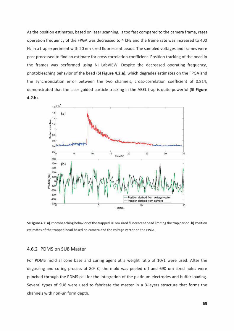
65
As the position estimates, based on laser scanning, is too fast compared to the camera frame, rates
operation frequency of the FPGA was decreased to 4 kHz and the frame rate was increased to 400
Hz in a trap experiment with 20 nm sized fluorescent beads. The sampled voltages and frames were
post processed to find an estimate for cross correlation coefficient. Position tracking of the bead in
the frames was performed using NI LabVIEW. Despite the decreased operating frequency,
photobleaching behavior of the bead (SI Figure 4.2.a), which degrades estimates on the FPGA and
the synchronization error between the two channels, cross-correlation coefficient of 0.814,
demonstrated that the laser guided particle tracking in the ABEL trap is quite powerful (SI Figure
4.2.b).
SI Figure 4.2: a) Photobeaching behavior of the trapped 20 nm sized fluorescent bead limiting the trap period. b) Position
estimates of the trapped bead based on camera and the voltage vector on the FPGA.
4.6.2 PDMS on SU8 Master
For PDMS mold silicone base and curing agent at a weight ratio of 10/1 were used. After the
degassing and curing process at 80o C, the mold was peeled off and 690 um sized holes were
punched through the PDMS cell for the integration of the platinum electrodes and buffer loading.
Several types of SU8 were used to fabricate the master in a 3-layers structure that forms the
channels with non-uniform depth.

66
SI Figure 4.3: Layout of the SU8 master for ABEL trap microfluidics. The distance between the opposite ports for
electrodes is 1 cm and the trap center has a size of 50x50 um.
Double side polished Si wafers 100 mm in size were plasma cleaned in Tepla300 for 20 minutes.
GM1040 type SU8 was coated on the wafer with the following speed steps for 800 nm channel
thickness: 5s at 500 rpm/s, 40s at 5500 rpm/s, 1s at 6500 rpm/s, 5s at 5500 rpm/s with 100 rpm/s
ramp for all steps. After 1 minute of relaxation, the wafer was baked at 130 0C for 1 hour with 1 0C/min ramp. Then, 50 mW/cm2 of exposure was done with MA6 trough backside alignment. A post-
exposure bake at 90 0C for 15 minutes was performed for cross-linking before the second layer
coating. GM1060 type SU8 was used to form 4 um thick of the second layer with the following spin
steps: 5s at 500 rpm/s, 40s at 5000 rpm/s, 1s at 6000 rpm/s, 5s at 5000 rpm/s. The preceding process
was similar to the first step with the following changed parameters: 10 minutes of relaxation time,
2 hours of soft bake, 95 mW/cm2 of exposure, and 30 minutes of post-exposure bake. For a 50 um
thick third layer, GM1075 was used with the spin steps as follows: 5s at 500 rpm/s, 40s at 3800
rpm/s, 1s at 4800 rpm/s, 5s at 3800 rpm/s. The process was completed with the following changed
parameters: 10 minutes of relaxation time, 3 hours of soft bake, 120 mW/cm2 of exposure, and 1
hour of post-exposure bake. The master fabrication (SI Figure 4.3) was completed with the

67
simultaneous development of the layers in propylene glycol monomethyl ether acetate for 4 minutes
and a hard bake at 150 0C for 3 hours.
4.6.3 RF Circuit on Cover Glass
The dielectric constant of the cover glass measured with the capacitance value obtained through
thin metal evaporation on parallel surfaces of the material. The schematic of the circuit modelled on
TXline and COMSOL RF Module.
Piranha cleaned 120 um thick cover glasses 24x60 mm in size were attached to Si wafers using
quickstick135 for a double layer lift-off process. 200 nm of Cr and 800 nm of Al evaporated with
LAB600H to pattern the RF circuit. After the sonication step in the acetone bath, the cover glasses
were rinsed with isopropanol and DI water. 30 nm of Al2O3 was deposited on the circuit with ALD for
the electrical isolation. The isolated circuit was embedded in a PDMS layer of 4 um thickness to
provide a flat surface for the circuit and microfluidics integration. Using epoxy silver conductor (Ted
Pella), the SMA end launch connector (Digi-Key) was aligned and attached to the circuit under the
microscope. Finally, the circuit on the cover glass aligned with the trap center was formed in the
microfluidic cell under the microscope and bonded through the plasma treatment (SI Figure 4.4).
SI Figure 4.4: a) Modelled RF circuit schematic to be integrated to the PDMS cell. b) Photograph of the RF circuit
integrated microfluidic device used for ESR measurements in the ABEL trap.

68
4.6.4 ESR Spectrum of a Rotationally Diffusing FND with NV Defects
The total absorption from optical dipoles, and , that are orthogonally oriented [174, 175], with
respect to the NV symmetry, is , where and is the exciting electric field.
The collection efficiency, is limited by the critical angle of the microscope objective,
where is the numerical aperture and is the refractive index of water.
, where stands for the intensity of the dipole components orthogonal to
direction specified by and spherical angles. For the NV at a specific orientation with
respect to the magnetic field, the influence on the ground state Hamiltonian is
where , , are
magnetic field components and other parameters are as explained in the main text. To estimate the
photoluminescence spectrum of a rotationally diffusing FND in the ABEL trap, we integrated
intensity profiles of the particle with random orientations. Increasing the magnetic field strength
results in a separation in the frequency peaks with broadening and a decrease in the amplitudes
(Figure 4.4.b).

69
5. Conclusion and Outlook
In the scope of this PhD work, I tried to establish a connection between electrokinetic manipulation
and the diamond photonics. The ABEL trap technique has been selected as the manipulation tool
for several reasons.
First, single FNDs with NV defects are bright and stable particles that are not photo-bleaching. While
this property is not helpful for passive trapping techniques, such as optical tweezers, it fits very well
to the tracking scheme followed in the ABEL trap. In this case, the trap stiffness and the size of the
smallest particle that can be trapped are limited by the estimations and the active feedback
performed in the digital environment. Therefore, future advancements in the FPGA device
technology will enhance these parameters. An innovative solution for the speed enhancement
would be a design in an application-specific integrated circuit (ASIC) platform.
Second, the ABEL trap uses weak electrokinetic forces that are not resulting in excessive heating
and agglomerations. Moreover, the forces are not perturbative to the environment; all the
molecules floating in the buffer are subjected to the same feedback. These properties are well
matched to the quantum optic experiments carried on single FNDs.
Also, given that any physical support is not required, this technique is an outstanding alternative to
AFM-like probes that are not functional in closed fluidic environments. The three-dimensional ABEL
trap we proposed is able to manipulate single FNDs freely by diffusing in a fluidic volume. A potential
future work could be a laser guided tracking scheme also employed for the axial position detection.
One can perform time-shared excitations or multiple confocal detections on axial planes to extract
the particle position with better temporal and spatial resolution [176, 177].
One drawback of the current ABEL trap configuration is the requirement of the cleanroom process
for microfluidics. One potential solution would be glass nanocapillaries formed through a pipette
puller. More recently, our preliminary work demonstrated that such nanocapillaries can be used for
one-dimensional ABEL trap without any cleanroom process. A water-filled nonocapillary baked in
liquid PDMS generates bubbles on its two ends that can be used for direct integration of electrodes.
Besides its simplicity, nanocapillary configuration provides several advantages over the
manipulation in PDMS microfluidics. In contrast to the PDMS, glass material has a very low
background fluorescence noise. Furthermore, it does not adsorb molecules that may change the

70
surface quality. Given that glass is nonporous to oxygen, it will also reduce the quenching effect and
extend the trapping period.
A far-out idea for the ABEL trap engineering would be the realization of a compact chip scale device
that includes all the components required for a stable trapping. For instance, a micro
electromechanical mirror (MEMS technology) can provide the same functionality as the scanning
excitation optics, as shown in chapter 1. Similarly, a micro optical system for fluorescence detection
may replace the detection optics. Although the miniaturization process requires a long term effort,
once established it will be a very popular and practical tool for single particle studies.
After the realization of the ABEL trap, we have demonstrated the nanoscale magnetometry
application of single FNDs in aqueous environment. This achievement also verifies the compatibility
of the technique for other sensing and imaging applications single FNDs can provide. Besides the
established detection protocols given in chapter 2, a potential future work would be the
manipulation of functionalized aptamers coupled to single FNDs. If one end of a specific aptamer is
attached to a magnetic bead and the other end is attached to single FNDs, the strong magnetic field
will be reflected into the ODMR spectrum. As the proteins or lipids, specific to the aptamer, can
break this connection manipulation of such complexes, the ABEL trap can present bio-sensing
capability at the single molecule level. Compared to fluorescence resonance energy transfer (FRET)
experiments, this approach has several advantages. First, as we are using magnetic labelling, the
efficiency is not dependent on the donor-acceptor spectrum overlap. While in FRET experiments
the distance between the donor and the acceptor should be in nanometer scale, for the proposed
aptamer approach the ODMR signal only depends on the field generated from the magnetic particle,
see Figure 5.1. Moreover, unlike FRET experiments, here the alignment of molecular orientation is
not necessarily required. As the ABEL trap leads to an isotropic distribution in the particle
orientation in time, the corresponding magnetic field strength can be precisely resolved. Given that
enzyme-linked immunosorbent assay (ELIZA) technology is not providing required sensitivity for rare
antigens, such a modality can open up new paths in clinical detection. However, we still need to
investigate the temporal and spatial sensitivity of here proposed method to be able to fairly
compare two modalities.

71
Figure 5.1: The aptamer configuration of single FND and magnetic bead for molecular specific detection. A bio-molecule
that is modifying the aptamer will be visible in the ODMR spectrum.
The use of FNDs in aptamer configuration can also be employed in other single molecule techniques.
For instance, NV centers, as magnetic reporter, in force-induced remnant magnetization
spectroscopy (FIRMS) [178-180] can resolve noncovalent bonds between ligand-receptor
complexes. This may facilitate studies on different systems of different complexities, such as
protein-protein, protein-DNA, and DNA –DNA interactions. One possible configuration for the
integrated platform is presented in Figure 5.2.
Figure 5.2: The working principle of NV magnetometry based force-induced remnant magnetization spectroscopy
platform. 1, 2, 3 are standing for different ligand-receptor complexes. Different noncovalent bonds between the
complexes are broken at different perturbative force strengths, . The dissociation process is randomizing the
orientation of the magnetic particles that decreases the detected magnetization. NV centers provide optical detection
of the interactions with molecular specificity.
It is clear that this thesis has just set a ground for many exciting directions where ABEL trap-like
manipulation of single FNDs can be used in quantum sensing in the aqueous environments.

72
List of Acronyms
1D: one-dimensional
2D: two-dimensional
3D: three-dimensional
ABEL anti-Brownian electrokinetic trap
AFM: atomic force microscopy
DESM: deterministic emitter switch microscopy
FND: fluorescent nanodiamond
FP: fluorescent protein
FWHM: full width at half maximum
ISC intersystem crossing
NSOM: near-field scanning optical microscopy
NV: nitrogen vacancy
MRI: magnetic resonance imaging
MTB magnetotactic bacteria
ODMR: optically detected magnetic resonance
OT optical trap
QD quantum dot
PALM: photoactivated localization microscopy
PSB phonon side bands
RESOLFT: reversible saturable optical linear fluorescence transitions
SQUID: superconducting quantum interference device

73
SPT single particle tracking
STORM: stochastic optical reconstruction microscopy
ZFS: zero field splitting

74
References
1. Einstein, A., On the movement of small particles suspended in stationary liquids required by the molecular-kinetic theory of heat. Ann. d. Phys., 1905(17): p. 549-560.
2. Einstein, A., Über die von der molekularkinetischen Theorie der Wärme geforderte Bewegung von in ruhenden Flüssigkeiten suspendierten Teilchen. Annalen der Physik, 1905. 322(8): p. 549-560.
3. Webb, J.l.P., Einstein and Brownian motion-a student project. Physics Education, 1980. 15(2): p. 116. 4. Gaspard, P., et al., Experimental evidence for microscopic chaos. Nature, 1998. 394(6696): p. 865-868. 5. Slomson, A.B., Introduction to Combinatorics. 1997: CRC Press. 6. Ashkin, A., Forces of a single-beam gradient laser trap on a dielectric sphere in the ray optics regime. Biophysical Journal,
1992. 61(2): p. 569-582. 7. Ashkin, A., et al., Observation of a single-beam gradient force optical trap for dielectric particles. Optics Letters, 1986. 11(5):
p. 288-290. 8. Zemánek, P., A. Jonáš, and M. Liška, Simplified description of optical forces acting on a nanoparticle in the Gaussian standing
wave. Journal of the Optical Society of America A, 2002. 19(5): p. 1025-1034. 9. Seol, Y., A.E. Carpenter, and T.T. Perkins, Gold nanoparticles: enhanced optical trapping and sensitivity coupled with
significant heating. Optics Letters, 2006. 31(16): p. 2429-2431. 10. Krishnan, M., et al., Geometry-induced electrostatic trapping of nanometric objects in a fluid. Nature, 2010. 467(7316): p.
692-695. 11. Tran, S.B.Q., P. Marmottant, and P. Thibault, Fast acoustic tweezers for the two-dimensional manipulation of individual
particles in microfluidic channels. Applied Physics Letters, 2012. 101(11): p. 114103. 12. Harris, N.R., et al., A silicon microfluidic ultrasonic separator. Sensors and Actuators B: Chemical, 2003. 95(1–3): p. 425-434. 13. Tanyeri, M., et al., A microfluidic-based hydrodynamic trap: design and implementation. Lab on a Chip, 2011. 11(10): p.
1786-1794. 14. Guan, W., et al., Paul trapping of charged particles in aqueous solution. Proceedings of the National Academy of Sciences,
2011. 108(23): p. 9326-9330. 15. Smith, S., L. Finzi, and C. Bustamante, Direct mechanical measurements of the elasticity of single DNA molecules by using
magnetic beads. Science, 1992. 258(5085): p. 1122-1126. 16. Strick, T.R., et al., The Elasticity of a Single Supercoiled DNA Molecule. Science, 1996. 271(5257): p. 1835-1837. 17. van der Heijden, T., et al., Torque-limited RecA polymerization on dsDNA. Nucleic Acids Research, 2005. 33(7): p. 2099-2105. 18. Koster, D.A., et al., Antitumour drugs impede DNA uncoiling by topoisomerase I. Nature, 2007. 448(7150): p. 213-217. 19. Itoh, H., et al., Mechanically driven ATP synthesis by F1-ATPase. Nature, 2004. 427(6973): p. 465-468. 20. Gore, J., et al., Mechanochemical analysis of DNA gyrase using rotor bead tracking. Nature, 2006. 439(7072): p. 100-104. 21. Barbic, M., et al., Scanning probe electromagnetic tweezers. Applied Physics Letters, 2001. 79(12): p. 1897-1899. 22. Gosse, C. and V. Croquette, Magnetic tweezers: micromanipulation and force measurement at the molecular level.
Biophysical Journal, 2002. 82(6): p. 3314-3329. 23. Huckel, P.D.a.E., The Cataphoresis of the Sphere. Physikalische Zeitschrift, 1924(25): p. 204-210. 24. Fried, M. and D.M. Crothers, Equilibria and Kinetics of Lac Repressor-Operator Interactions by Polyacrylamide-Gel
Electrophoresis. Nucleic Acids Research, 1981. 9(23): p. 6505-6525. 25. Garner, M.M. and A. Revzin, A Gel-Electrophoresis Method for Quantifying the Binding of Proteins to Specific DNA Regions
- Application to Components of the Escherichia-Coli Lactose Operon Regulatory System. Nucleic Acids Research, 1981. 9(13): p. 3047-3060.
26. Chen, M.L., Two-dimensional gel electrophoresis revealed antipsychotic drugs induced protein expression modulations in C6 glioma cells. Prog Neuropsychopharmacol Biol Psychiatry, 2013. 40: p. 1-11.
27. Xi, J., X.A. Si, and R. Gaide, Electrophoretic Particle Guidance Significantly Enhances Olfactory Drug Delivery: A Feasibility Study. PLoS ONE, 2014. 9(1): p. e86593.
28. Swerdlow, H. and R. Gesteland, Capillary gel electrophoresis for rapid, high resolution DNA sequencing. Nucleic Acids Research, 1990. 18(6): p. 1415-1419.
29. Karger, B.L. and A. Guttman, DNA Sequencing by Capillary Electrophoresis. Electrophoresis, 2009. 30(Suppl 1): p. S196-S202. 30. von Smoluchowski, M., Zur kinetischen Theorie der Brownschen Molekularbewegung und der Suspensionen. Annalen der
Physik, 1906. 326(14): p. 756-780. 31. Nie, F.-Q., et al., Robust monolithic silica-based on-chip electro-osmotic micro-pump. Analyst, 2007. 132(5): p. 417-424. 32. Meisel, I. and P. Ehrhard, Electrically-excited (electroosmotic) flows in microchannels for mixing applications. European
Journal of Mechanics - B/Fluids, 2006. 25(4): p. 491-504. 33. Henry, D.C., The Cataphoresis of Suspended Particles. Part I. The Equation of Cataphoresis. Proceedings of the Royal Society
of London A: Mathematical, Physical and Engineering Sciences, 1931. 133(821): p. 106-129. 34. Wang, Q. and W.E. Moerner, Optimal strategy for trapping single fluorescent molecules in solution using the ABEL trap.
Applied Physics B-Lasers and Optics, 2010. 99(1-2): p. 23-30. 35. Cohen, A.E. and W.E. Moerner, Principal-components analysis of shape fluctuations of single DNA molecules. Proceedings
of the National Academy of Sciences, 2007. 104(31): p. 12622-12627. 36. Goldsmith, R.H. and W.E. Moerner, Watching conformational- and photodynamics of single fluorescent proteins in solution.
Nat Chem, 2010. 2(3): p. 179-186. 37. Quimby, R.S., Photonics and Lasers: An Introduction. 2006, John Wiley & Sons. p. 323.
75
38. Sergio Martellucci, M.S., Free and Guided Optical Beams. 2004, World Scientific. p. 66. 39. Kalman, R.E., A New Approach to Linear Filtering and Prediction Problems. Transactions of the ASME – Journal of Basic
Engineering, 1960(82 (Series D)): p. 35-45. 40. Galanis, G., et al., Applications of Kalman filters based on non-linear functions to numerical weather predictions. Annales
Geophysicae, 2006. 24: p. 2451-2460. 41. Foytik, J., P. Sankaran, and V. Asari, Tracking and Recognizing Multiple Faces Using Kalman Filter and ModularPCA Procedia
Computer Science 2011. 6: p. 256 - 261. 42. Walther, B., A. May, and T. Fischer, Fitting Yield Curve Models Using the Kalman Filter. PAMM, 2003. 3(1): p. 507-508. 43. Fantian, K., et al. Mobile Robot Localization Based on Extended Kalman Filter. in Intelligent Control and Automation, 2006.
WCICA 2006. The Sixth World Congress on. 2006. 44. Chalfie, M., et al., Green fluorescent protein as a marker for gene-expression. Science, 1994. 263(5148): p. 802-805. 45. Griffin, B.A., S.R. Adams, and R.Y. Tsien, Specific covalent labeling of recombinant protein molecules inside live cells. Science,
1998. 281(5374): p. 269-272. 46. Chan, W.C.W. and S.M. Nie, Quantum dot bioconjugates for ultrasensitive nonisotopic detection. Science, 1998. 281(5385):
p. 2016-2018. 47. Miyawaki, A., A. Sawano, and T. Kogure, Lighting up cells: labelling proteins with fluorophores. Nature Cell Biology, 2003: p.
S1-S7. 48. Giepmans, B.N.G., et al., Review - The fluorescent toolbox for assessing protein location and function. Science, 2006.
312(5771): p. 217-224. 49. Chang, Y.R., et al., Mass production and dynamic imaging of fluorescent nanodiamonds. Nature Nanotechnology, 2008.
3(5): p. 284-288. 50. Yu, S.J., et al., Bright fluorescent nanodiamonds: No photobleaching and low cytotoxicity. Journal of the American Chemical
Society, 2005. 127(50): p. 17604-17605. 51. Wu, T.J., et al., Tracking the engraftment and regenerative capabilities of transplanted lung stem cells using fluorescent
nanodiamonds. Nature Nanotechnology, 2013. 8(9): p. 682-689. 52. Tisler, J., et al., Highly Efficient FRET from a Single Nitrogen-Vacancy Center in Nanodiamonds to a Single Organic Molecule.
Acs Nano, 2011. 5(10): p. 7893-7898. 53. Vaijayanthimala, V., et al., The long-term stability and biocompatibility of fluorescent nanodiamond as an in vivo contrast
agent. Biomaterials, 2012. 33(31): p. 7794-7802. 54. Han, K.Y., et al., Three-Dimensional Stimulated Emission Depletion Microscopy of Nitrogen-Vacancy Centers in Diamond
Using Continuous-Wave Light. Nano Letters, 2009. 9(9): p. 3323-3329. 55. Balasubramanian, G., et al., Nanoscale imaging magnetometry with diamond spins under ambient conditions. Nature, 2008.
455(7213): p. 648-U46. 56. Dolde, F., et al., Electric-field sensing using single diamond spins. Nature Physics, 2011. 7(6): p. 459-463. 57. Ziem, F.C., et al., Highly Sensitive Detection of Physiological Spins in a Microfluidic Device. Nano Letters, 2013. 13(9): p.
4093-4098. 58. Kucsko, G., et al., Nanometre-scale thermometry in a living cell. Nature, 2013. 500(7460): p. 54-U71. 59. Shi, F., et al., Protein imaging. Single-protein spin resonance spectroscopy under ambient conditions. Science, 2015.
347(6226): p. 1135-8. 60. Aharonovich, I., et al., Diamond-based single-photon emitters. Reports on Progress in Physics, 2011. 74(7). 61. Kayci, M., H.C. Chang, and A. Radenovic, Electron Spin Resonance of Nitrogen-Vacancy Defects Embedded in Single
Nanodiamonds in an ABEL Trap. Nano Letters, 2014. 14(9): p. 5335-5341. 62. Smith, B.R., et al., Five-Nanometer Diamond with Luminescent Nitrogen-Vacancy Defect Centers. Small, 2009. 5(14): p.
1649-1653. 63. Fu, C.C., et al., Characterization and application of single fluorescent nanodiamonds as cellular biomarkers. Proceedings of
the National Academy of Sciences of the United States of America, 2007. 104(3): p. 727-732. 64. Guillois, O., G. Ledoux, and C. Reynaud, Diamond infrared emission bands in circumstellar media. Astrophysical Journal,
1999. 521(2): p. L133-L136. 65. Goto, M., et al., SPATIALLY RESOLVED 3 mu m SPECTROSCOPY OF ELIAS 1: ORIGIN OF DIAMONDS IN PROTOPLANETARY
DISKS. Astrophysical Journal, 2009. 693(1): p. 610-616. 66. Vlasov, I.I., et al., Molecular-sized fluorescent nanodiamonds. Nature Nanotechnology, 2014. 9(1): p. 54-58. 67. Chang, Y.R., et al., Mass production and dynamic imaging of fluorescent nanodiamonds. Nature Nanotechnology, 2008.
3(5): p. 284-8. 68. Bradac, C., et al., Observation and control of blinking nitrogen-vacancy centres in discrete nanodiamonds. Nature
Nanotechnology, 2010. 5(5): p. 345-349. 69. Acosta, V.M., et al., Temperature Dependence of the Nitrogen-Vacancy Magnetic Resonance in Diamond. Physical Review
Letters, 2010. 104(7). 70. Doherty, M.W., et al., Electronic Properties and Metrology Applications of the Diamond NV- Center under Pressure. Physical
Review Letters, 2014. 112(4). 71. Steinert, S., et al., Magnetic spin imaging under ambient conditions with sub-cellular resolution. Nature Communications,
2013. 4. 72. Childress, L., R. Walsworth, and M. Lukin, Atom-like crystal defects: From quantum computers to biological sensors. Physics
Today, 2014. 67(10): p. 38-43. 73. Chang, I.P., K.C. Hwang, and C.S. Chiang, Preparation of Fluorescent Magnetic Nanodiamonds and Cellular Imaging. Journal
of the American Chemical Society, 2008. 130(46): p. 15476-15481.

76
74. Hartl, A., et al., Protein-modified nanocrystalline diamond thin films for biosensor applications. Nature materials, 2004. 3(10): p. 736-42.
75. Yang, W., et al., DNA-modified nanocrystalline diamond thin-films as stable, biologically active substrates. Nature materials, 2002. 1(4): p. 253-7.
76. Bumb, A., et al., Silica encapsulation of fluorescent nanodiamonds for colloidal stability and facile surface functionalization. Journal of the American Chemical Society, 2013. 135(21): p. 7815-8.
77. Resch-Genger, U., et al., Quantum dots versus organic dyes as fluorescent labels. Nature Methods, 2008. 5(9): p. 763-775. 78. Tisler, J., et al., Fluorescence and Spin Properties of Defects in Single Digit Nanodiamonds. Acs Nano, 2009. 3(7): p. 1959-
1965. 79. Weber, G., Fluorescence of riboflavin and flavin-adenine dinucleotide. The Biochemical journal, 1950. 47(1): p. 114-121. 80. Gohar, A.V., et al., Subcellular localization-dependent changes in EGFP fluorescence lifetime measured by time-resolved flow
cytometry. Biomedical Optics Express, 2013. 4(8): p. 1390-1400. 81. Sanchez-Andres, A., Y. Chen, and J.D. Muller, Molecular brightness determined from a generalized form of Mandel's Q-
parameter. Biophysical Journal, 2005. 89(5): p. 3531-3547. 82. Chen, Y., et al., Molecular brightness characterization of EGFP in vivo by fluorescence fluctuation spectroscopy. Biophysical
Journal, 2002. 82(1): p. 133-144. 83. Gaebel, T., et al., Room-temperature coherent coupling of single spins in diamond. Nature Physics, 2006. 2(6): p. 408-413. 84. Santori, C., et al., Indistinguishable photons from a single-photon device. Nature, 2002. 419(6907): p. 594-597. 85. He, Y.M., et al., On-demand semiconductor single-photon source with near-unity indistinguishability. Nature
Nanotechnology, 2013. 8(3): p. 213-217. 86. Wilson, A.C., et al., Tunable spin-spin interactions and entanglement of ions in separate potential wells. Nature, 2014.
512(7512): p. 57-+. 87. Taylor, J.M., et al., High-sensitivity diamond magnetometer with nanoscale resolution. Nature Physics, 2008. 4(10): p. 810-
816. 88. Maze, J.R., et al., Nanoscale magnetic sensing with an individual electronic spin in diamond. Nature, 2008. 455(7213): p.
644-U41. 89. Bending, S.J., Local magnetic probes of superconductors. Advances in Physics, 1999. 48(4): p. 449-535. 90. Chang, A.M., et al., Scanning Hall-Probe Microscopy of a Vortex and Field Fluctuations in La1.85sr0.15cuo4 Films.
Europhysics Letters, 1992. 20(7): p. 645-650. 91. Budker, D., et al., Resonant nonlinear magneto-optical effects in atoms. Reviews of Modern Physics, 2002. 74(4): p. 1153-
1201. 92. Mamin, H.J., et al., Nuclear magnetic resonance imaging with 90-nm resolution. Nature Nanotechnology, 2007. 2(5): p. 301-
306. 93. Martin, Y., D.W. Abraham, and H.K. Wickramasinghe, High-Resolution Capacitance Measurement and Potentiometry by
Force Microscopy. Applied Physics Letters, 1988. 52(13): p. 1103-1105. 94. Neumann, P., et al., High-Precision Nanoscale Temperature Sensing Using Single Defects in Diamond. Nano Letters, 2013.
13(6): p. 2738-2742. 95. Grinolds, M.S., et al., Subnanometre resolution in three-dimensional magnetic resonance imaging of individual dark spins.
Nature Nanotechnology, 2014. 9(4): p. 279-284. 96. Vanoort, E. and M. Glasbeek, Electric-Field-Induced Modulation of Spin Echoes of N-V Centers in Diamond. Chemical Physics
Letters, 1990. 168(6): p. 529-532. 97. Schirhagl, R., et al., Nitrogen-Vacancy Centers in Diamond: Nanoscale Sensors for Physics and Biology. Annual Review of
Physical Chemistry, Vol 65, 2014. 65: p. 83-105. 98. Mohan, N., et al., In vivo imaging and toxicity assessments of fluorescent nanodiamonds in Caenorhabditis elegans. Nano
Letters, 2010. 10(9): p. 3692-9. 99. Simpson, D.A., et al., In vivo imaging and tracking of individual nanodiamonds in drosophila melanogaster embryos.
Biomedical Optics Express, 2014. 5(4): p. 1250-1261. 100. Igarashi, R., et al., Real-Time Background-Free Selective Imaging of Fluorescent Nanodiamonds in Vivo. Nano Letters, 2012.
12(11): p. 5726-5732. 101. Chang, C.C., et al., Exploring cytoplasmic dynamics in zebrafish yolk cells by single particle tracking of fluorescent
nanodiamonds. Advances in Photonics of Quantum Computing, Memory, and Communication V, 2012. 8272. 102. Huang, Y.A., et al., The effect of fluorescent nanodiamonds on neuronal survival and morphogenesis. Scientific Reports,
2014. 4. 103. Hui, Y.Y., et al., Wide-field imaging and flow cytometric analysis of cancer cells in blood by fluorescent nanodiamond labeling
and time gating. Scientific Reports, 2014. 4. 104. McGuinness, L.P., et al., Quantum measurement and orientation tracking of fluorescent nanodiamonds inside living cells.
Nature Nanotechnology, 2011. 6(6): p. 358-363. 105. Manus, L.M., et al., Gd(III)-nanodiamond conjugates for MRI contrast enhancement. Nano Letters, 2010. 10(2): p. 484-9. 106. Deschout, H., et al., Precisely and accurately localizing single emitters in fluorescence microscopy. Nature Methods, 2014.
11(3): p. 253-266. 107. Rittweger, E., et al., STED microscopy reveals crystal colour centres with nanometric resolution. Nature Photonics, 2009.
3(3): p. 144-147. 108. Kuhn, S., et al., Diamond colour centres as a nanoscopic light source for scanning near-field optical microscopy. Journal of
Microscopy-Oxford, 2001. 202: p. 2-6. 109. Nakayama, Y., et al., Tunable nanowire nonlinear optical probe. Nature, 2007. 447(7148): p. 1098-U8. 110. Dutto, F., et al., Nonlinear Optical Response in Single Alkaline Niobate Nanowires. Nano Letters, 2011. 11(6): p. 2517-2521.
77
111. Dutto, F. and A. Radenovic, Alkaline niobate nanowires as opto-mechanical probes. Optical Trapping and Optical Micromanipulation Ix, 2012. 8458.
112. Macias-Romero, C., et al., Probing Rotational and Translational Diffusion of Nanodoublers in Living Cells on Microsecond Time Scales. Nano Letters, 2014. 14(5): p. 2552-2557.
113. Mor, F.M., et al., Upconversion Particle as a Local Luminescent Brownian Probe: A Photonic Force Microscopy Study. Acs Photonics, 2014. 1(12): p. 1251-1257.
114. Betzig, E., et al., Near-Field Scanning Optical Microscopy (Nsom) - Development and Biophysical Applications. Biophysical Journal, 1986. 49(1): p. 269-279.
115. Durig, U., D.W. Pohl, and F. Rohner, Near-Field Optical-Scanning Microscopy. Journal of Applied Physics, 1986. 59(10): p. 3318-3327.
116. Betzig, E., et al., Breaking the Diffraction Barrier - Optical Microscopy on a Nanometric Scale. Science, 1991. 251(5000): p. 1468-1470.
117. Sonnefraud, Y., et al., Diamond nanocrystals hosting single nitrogen-vacancy color centers sorted by photon-correlation near-field microscopy. Optics Letters, 2008. 33(6): p. 611-613.
118. Einstein, A., Strahlungs-Emission und -Absorption nach der Quantentheorie. Deutsche Physikalische Gesellschaft, 1916. 18: p. 318-323.
119. Hell, S.W. and J. Wichmann, Breaking the Diffraction Resolution Limit by Stimulated-Emission - Stimulated-Emission-Depletion Fluorescence Microscopy. Optics Letters, 1994. 19(11): p. 780-782.
120. Klar, T.A. and S.W. Hell, Subdiffraction resolution in far-field fluorescence microscopy. Optics Letters, 1999. 24(14): p. 954-6.
121. Hell, S.W., Far-field optical nanoscopy. Science, 2007. 316(5828): p. 1153-1158. 122. Arroyo-Camejo, S., et al., Stimulated emission depletion microscopy resolves individual nitrogen vacancy centers in diamond
nanocrystals. Acs Nano, 2013. 7(12): p. 10912-9. 123. Maurer, P.C., et al., Far-field optical imaging and manipulation of individual spins with nanoscale resolution. Nature Physics,
2010. 6(11): p. 912-918. 124. Betzig, E., et al., Imaging intracellular fluorescent proteins at nanometer resolution. Science, 2006. 313(5793): p. 1642-1645. 125. Hess, S.T., T.P.K. Girirajan, and M.D. Mason, Ultra-high resolution imaging by fluorescence photoactivation localization
microscopy. Biophysical Journal, 2006. 91(11): p. 4258-4272. 126. Rust, M.J., M. Bates, and X.W. Zhuang, Sub-diffraction-limit imaging by stochastic optical reconstruction microscopy
(STORM). Nature Methods, 2006. 3(10): p. 793-795. 127. Chen, E.H., et al., Wide-Field Multispectral Super-Resolution Imaging Using Spin-Dependent Fluorescence in Nanodiamonds.
Nano Letters, 2013. 13(5): p. 2073-2077. 128. Le Sage, D., et al., Optical magnetic imaging of living cells. Nature, 2013. 496(7446): p. 486-U105. 129. Eder, S.H.K., et al., Magnetic characterization of isolated candidate vertebrate magnetoreceptor cells. Proceedings of the
National Academy of Sciences of the United States of America, 2012. 109(30): p. 12022-12027. 130. Cuche, A., et al., Near-field optical microscopy with a nanodiamond-based single-photon tip. Optics Express, 2009. 17(22):
p. 19969-19980. 131. Fedotov, I.V., et al., Electron spin manipulation and readout through an optical fiber. Scientific Reports, 2014. 4. 132. Maletinsky, P., et al., A robust scanning diamond sensor for nanoscale imaging with single nitrogen-vacancy centres. Nature
Nanotechnology, 2012. 7(5): p. 320-324. 133. Degen, C.L., Scanning magnetic field microscope with a diamond single-spin sensor. Applied Physics Letters, 2008. 92(24). 134. Ofori-Okai, B.K., et al., Spin properties of very shallow nitrogen vacancy defects in diamond. Physical Review B, 2012. 86(8). 135. Horowitz, V.R., et al., Electron spin resonance of nitrogen-vacancy centers in optically trapped nanodiamonds. Proceedings
of the National Academy of Sciences of the United States of America, 2012. 109(34): p. 13493-13497. 136. Geiselmann, M., et al., Three-dimensional optical manipulation of a single electron spin. Nature Nanotechnology, 2013.
8(3): p. 175-179. 137. Svoboda, K. and S.M. Block, Optical Trapping of Metallic Rayleigh Particles. Optics Letters, 1994. 19(13): p. 930-932. 138. Fields, A.P. and A.E. Cohen, Electrokinetic trapping at the one nanometer limit. Proceedings of the National Academy of
Sciences of the United States of America, 2011. 108(22): p. 8937-8942. 139. Maclaurin, D., et al., Nanoscale magnetometry through quantum control of nitrogen-vacancy centres in rotationally
diffusing nanodiamonds. New Journal of Physics, 2013. 15. 140. Geiselmann, M., et al., Three-dimensional optical manipulation of a single electron spin. Nat Nanotechnol, 2013. 8(3): p.
175-9. 141. Peterman, E.J., F. Gittes, and C.F. Schmidt, Laser-induced heating in optical traps. Biophys J, 2003. 84(2 Pt 1): p. 1308-16. 142. Gosse, C. and V. Croquette, Magnetic tweezers: micromanipulation and force measurement at the molecular level. Biophys
J, 2002. 82(6): p. 3314-29. 143. Wu, M.C., Optoelectronic tweezers. Nature Photonics, 2011. 5(6): p. 322-324. 144. Tran, S.B.Q., P. Marmottant, and P. Thibault, Fast acoustic tweezers for the two-dimensional manipulation of individual
particles in microfluidic channels. Applied Physics Letters, 2012. 101(11). 145. Guan, W.H., et al., Paul trapping of charged particles in aqueous solution. Proceedings of the National Academy of Sciences
of the United States of America, 2011. 108(23): p. 9326-9330. 146. Zhuang, Z.Y., et al., The effect of surface tethering on the folding of the src-SH3 protein domain. Physical Biology, 2009. 6(1). 147. King, J.K., Three-Dimensional Electrokinetic Trapping of a Single Fluorescent Nanoparticle in Solution, 2013. 148. Bockenhauer, S.D. and W.E. Moerner, Photo-induced conformational flexibility in single solution-phase peridinin-
chlorophyll-proteins. The journal of physical chemistry. A, 2013. 117(35): p. 8399-406. 149. Cohen, A.E. and W.E. Moerner. An all-glass microfluidic cell for the ABEL trap: fabrication and modeling. 2005.
78
150. King, J.K., B.K. Canfield, and L.M. Davis, Three-dimensional anti-Brownian electrokinetic trapping of a single nanoparticle in solution. Applied Physics Letters, 2013. 103(4): p. 043102.
151. Speidel, M., A. Jonas, and E.L. Florin, Three-dimensional tracking of fluorescent nanoparticles with subnanometer precision by use of off-focus imaging. Optics Letters, 2003. 28(2): p. 69-71.
152. Kayci, M., H.-C. Chang, and A. Radenovic, Electron spin resonance of nitrogen-vacancy defects embedded in single nanodiamonds in an ABEL trap. Nano letters, 2014. 14(9): p. 5335-5341.
153. Davies, G. and M.F. Hamer, Optical Studies of 1.945 Ev Vibronic Band in Diamond. Proceedings of the Royal Society of London Series a-Mathematical and Physical Sciences, 1976. 348(1653): p. 285-298.
154. Gruber, A., et al., Scanning confocal optical microscopy and magnetic resonance on single defect centers. Science, 1997. 276(5321): p. 2012-2014.
155. Babinec, T.M., et al., A diamond nanowire single-photon source. Nature Nanotechnology, 2010. 5(3): p. 195-199. 156. Englund, D., et al., Deterministic Coupling of a Single Nitrogen Vacancy Center to a Photonic Crystal Cavity. Nano Letters,
2010. 10(10): p. 3922-3926. 157. Pauzauskie, P.J., et al., Optical trapping and integration of semiconductor nanowire assemblies in water. Nature Materials,
2006. 5(2): p. 97-101. 158. Ashkin, A., Optical trapping and manipulation of neutral particles using lasers. Proc. Natl. Acad. Sci. USA, 1997. 94: p. 4853-
4860. 159. Cohen, A.E. and W.E. Moerner, Method for trapping and manipulating nanoscale objects in solution. Applied Physics Letters,
2005. 86(9). 160. Wang, Q., et al., Probing Single Biomolecules in Solution Using the Anti-Brownian Electrokinetic (ABEL) Trap. Accounts of
Chemical Research, 2012. 45(11): p. 1955-1964. 161. A.P. Fields, A.E.C., Anti-Brownian Traps for Studies on Single Molecules, in Methods in Enzymology, E. Inc., Editor. 2010. 162. Cohen, A.E. and W.E. Moerner, Principal-components analysis of shape fluctuations of single DNA molecules. Proceedings
of the National Academy of Sciences of the United States of America, 2007. 104(31): p. 12622-12627. 163. Wang, Q. and W.E. Moerner, An Adaptive Anti-Brownian Electrokinetic Trap with Real-Time Information on Single-Molecule
Diffusivity and Mobility. Acs Nano, 2011. 5(7): p. 5792-5799. 164. Goldsmith, R.H. and W.E. Moerner, Watching conformational- and photodynamics of single fluorescent proteins in solution.
Nature Chemistry, 2010. 2(3): p. 179-186. 165. Bockenhauer, S., et al., Conformational Dynamics of Single G Protein-Coupled Receptors in Solution. Journal of Physical
Chemistry B, 2011. 115(45): p. 13328-13338. 166. Wang, Q. and W.E. Moerner, Lifetime and Spectrally Resolved Characterization of the Photodynamics of Single Fluorophores
in Solution Using the Anti-Brownian Electrokinetic Trap. Journal of Physical Chemistry B, 2013. 117(16): p. 4641-4648. 167. Rendler, T., et al., Monitoring single membrane protein dynamics in a liposome manipulated in solution by the ABELtrap.
Imaging, Manipulation, and Analysis of Biomolecules, Cells, and Tissues Ix, 2011. 7902. 168. Mochalin, V.N., et al., The properties and applications of nanodiamonds. Nature Nanotechnology, 2012. 7(1): p. 11-23. 169. Felton, S., et al., Hyperfine interaction in the ground state of the negatively charged nitrogen vacancy center in diamond.
Physical Review B, 2009. 79(7). 170. Smeltzer, B., J. McIntyre, and L. Childress, Robust control of individual nuclear spins in diamond. Physical Review A, 2009.
80(5). 171. Steiner, M., et al., Universal enhancement of the optical readout fidelity of single electron spins at nitrogen-vacancy centers
in diamond. Physical Review B, 2010. 81(3). 172. Acosta, V.M., et al., Broadband magnetometry by infrared-absorption detection of nitrogen-vacancy ensembles in diamond.
Applied Physics Letters, 2010. 97(17). 173. Simon, D., Optimal state estimation: Kalman, H infinity, and nonlinear approaches. 2006: John Wiley & Sons. 174. Epstein, R.J., et al., Anisotropic interactions of a single spin and dark-spin spectroscopy in diamond. Nature Physics, 2005.
1(2): p. 94-98. 175. Dumeige, Y., et al., Controling the single-diamond nitrogen-vacancy color center photoluminescence spectrum with a Fabry-
Perot microcavity. New Journal of Physics, 2011. 13. 176. Cang, H., C. Shan Xu, and H. Yang, Progress in single-molecule tracking spectroscopy. Chemical Physics Letters, 2008. 457(4–
6): p. 285-291. 177. Wells, N.P., et al., Time-Resolved Three-Dimensional Molecular Tracking in Live Cells. Nano Letters, 2010. 10(11): p. 4732-
4737. 178. Yao, L. and S. Xu, Force-Induced Remnant Magnetization Spectroscopy for Specific Magnetic Imaging of Molecules.
Angewandte Chemie International Edition, 2011. 50(19): p. 4407-4409. 179. De Silva, L., et al., Well-Defined and Sequence-Specific Noncovalent Binding Forces of DNA. The Journal of Physical Chemistry
B, 2013. 117(25): p. 7554-7558. 180. De Silva, L., L. Yao, and S. Xu, Mechanically resolving noncovalent bonds using acoustic radiation force. Chemical
Communications, 2014. 50(74): p. 10786-10789.

79
Metin Kayci
[email protected], +41786920488
Education & Experiences
9/2011-present Ph.D. in Photonics
Ecole Polytechnique Fédérale de Lausanne -EPFL- (Switzerland)
Thesis: Nanoscale magnetometry with single FNDs manipulated in Anti-
Brownian electrokinetic trap.
5/2010-9/2010 Summer Research at MIT, EECS department (USA).
Implementation of a compact optoelectronic neural coprocessor
(CONCOP).
9/2007-6/2011 B.Sc. in Electronics Engineering (ranked 1st), minor in Physics (ranked 1st)
Sabanci University (Turkey)
Skills
Technical Photolithography, e-beam lithography, thin film deposition, dry and wet
etching, soft lithography, microfluidics design/fabrication, free-space
optics, fluorescence microscopy, nonlinear optics, RF circuit
design/fabrication, MEMS.
Computation FPGA, C++, LabVIEW, Matlab, COMSOL Multiphysics, SOLIDWORKS,
ImageJ, CAD
Academic works
Spring 2011-2013 Fundamental of bio-photonics (TA)
Fall 2010-2011 Optoelectronics (TA)
Spring 2009-2010 Electronic circuits II (TA)

80
Publications
Journal Articles
1. M. Kayci, A. Radenovic. Single fluorescent nanodiamond in a three-dimensional ABEL
trap. Scientific Reports (1015)
2. M. Kayci, H.C. Chang, A. Radenovic. Electron Spin Resonance of Nitrogen-Vacancy
Defects Embedded in Single Nanodiamonds in an ABEL Trap. Nano Letters (2014)
3. O. L. Sanchez, D. Lembke, M. Kayci, A. Radenovic & A. Kis. Ultrasensitive photodetectors
based on monolayer MoS2. Nature Nanotechnology (2013)
Oral Presentations
1. Single nano diamonds as scanning magnetometer in a fluidic environment, ENEFM &
INTERM 2015, Mugla (Turkey), October 19th-23rd 2015.
2. Optically detected magnetic resonance spectrum of single FNDs in aqueous medium,
ICDCM 2014, Madrid (spain), September 7th-11th 2014.
3. Electron spin resonance of nitrogen-vacancy centers in single nano diamond particles,
NDNC 2014, Chicago (USA), May 25th-29th 2014.
Posters
1. RF antenna integrated ABEL trap for electron spin resonance measurements, EPFL
Photonics Day, Lausanne, November 14th 2014.
2. Electrokinetic trap of nano-scale particles in microfluidics, Joint Annual Meeting of the
Austrian Physical Society and the Swiss Physical Society, Linz (Austria), September 3rd-6th
2013.
3. Nanopore integrated Anti-Brownian Electrokinetic trap, Swiss Single Molecule
Localization Microscopy Symposium, Lausanne (Switzerland), August 29th-31st 2012.
Languages: Kurdish (native), Turkish, English


![Bibliography - rd.springer.com978-3-0348-8954-4/1.pdf · 138 Bibliography [128] Y. Hu: Sur le mouvement brownien: calculs de lois, etudes asymptotiques, filtra tions, relations avec](https://img.pdfslide.us/doc/110x75/5e81a9940b29a074de117076/bibliography-rd-978-3-0348-8954-41pdf-138-bibliography-128-y-hu-sur-le.jpg)
![Chemical and Biological Applications of Digital ... · Microfluidique Discre´te pour Applications Biologiques [SAW Platform Dedicated to Discrete Microfluidics for Biological Applications],’’](https://img.pdfslide.us/doc/110x75/5f4674f61418344dec284931/chemical-and-biological-applications-of-digital-microfluidique-discrete-pour.jpg)